

Page 1
If you need more information on Computer and Electronic Repair, please visit these
in fact
websites to improve yourself.
http://www.fastrepairguide.com
http://www.protech2u.com
http://www.plasma-television-repair.com
http://www.lcd-television-repair.com
Happy Repairing!!
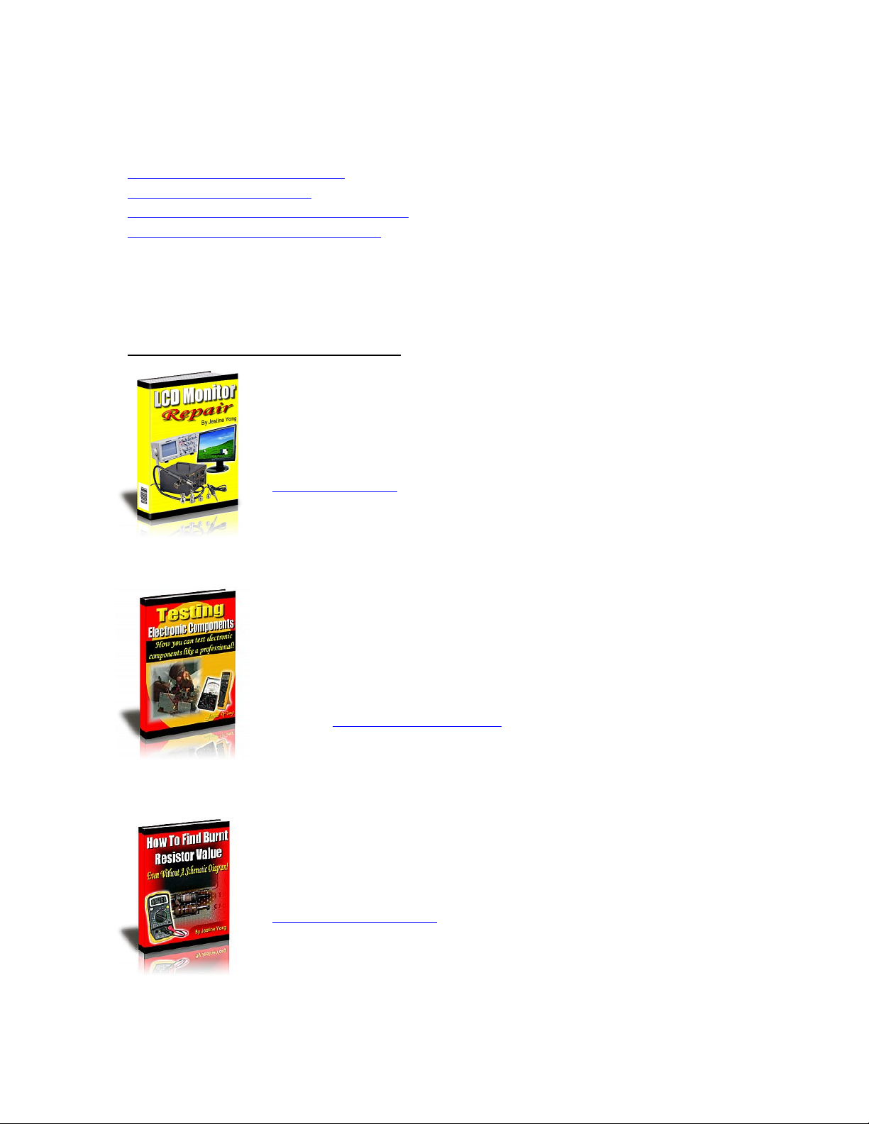
Highly Recommended Repair Ebook:
If you’re a LCD Monitor repairer, then this is the best guide for you.
Why? Because, the author revealed all his LCD Monitor Repairing
secrets for you. I think, with just few Repair tips you learned from
this guide you will get back your investment!
Click Here to read more.
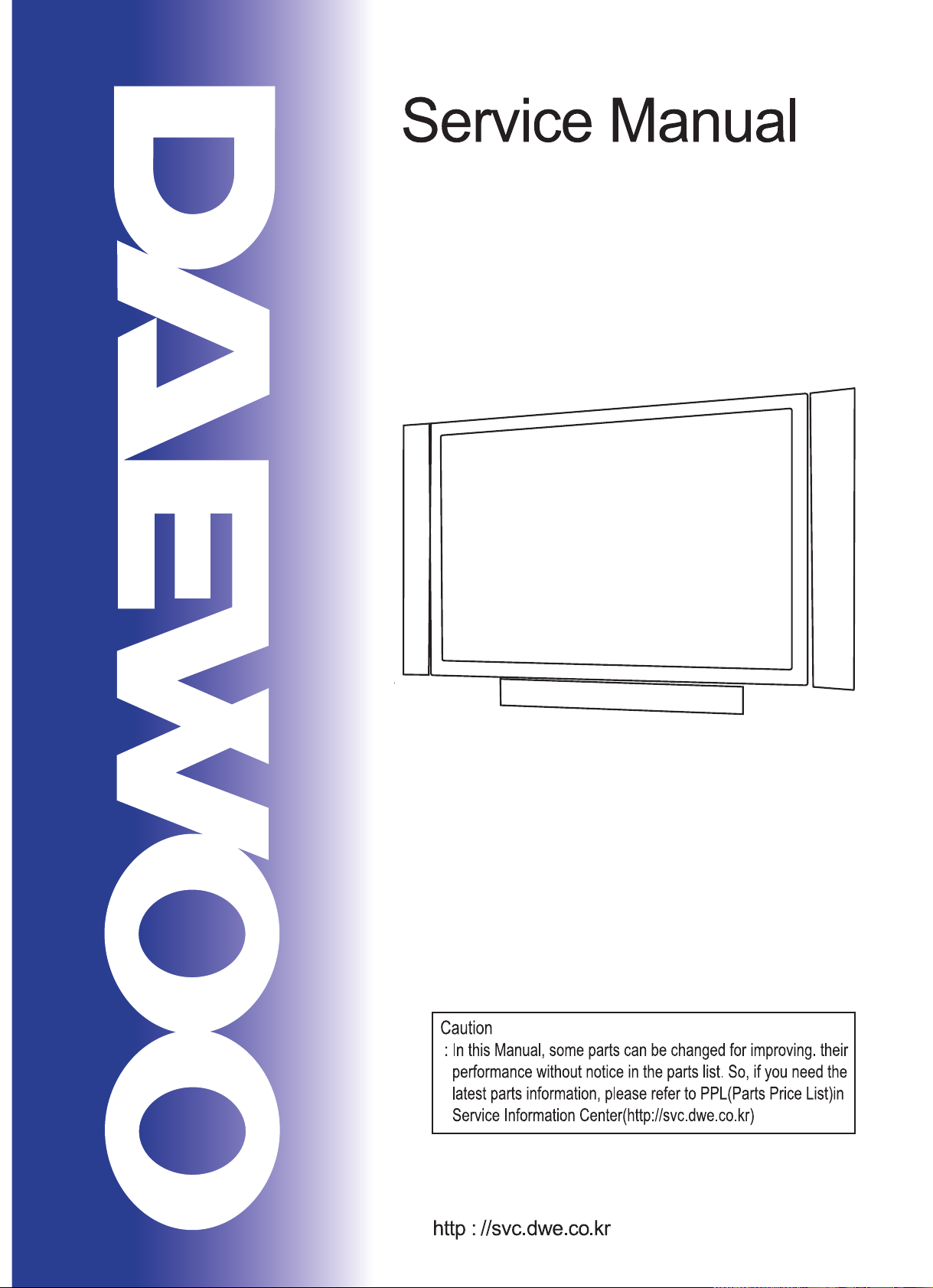
This eBook will show you how to test the electronic component
correctly and accurately. Some of you may say that I don’t
need this eBook because it is too simple! Do you know that,
there is lots of testing electronic components secrets I have learned
from this guide? Do you know how to test a‘TRIAC’ correctly and
accurately? If you answer no then I guess you have to get this
EBook. Click Here to read more.
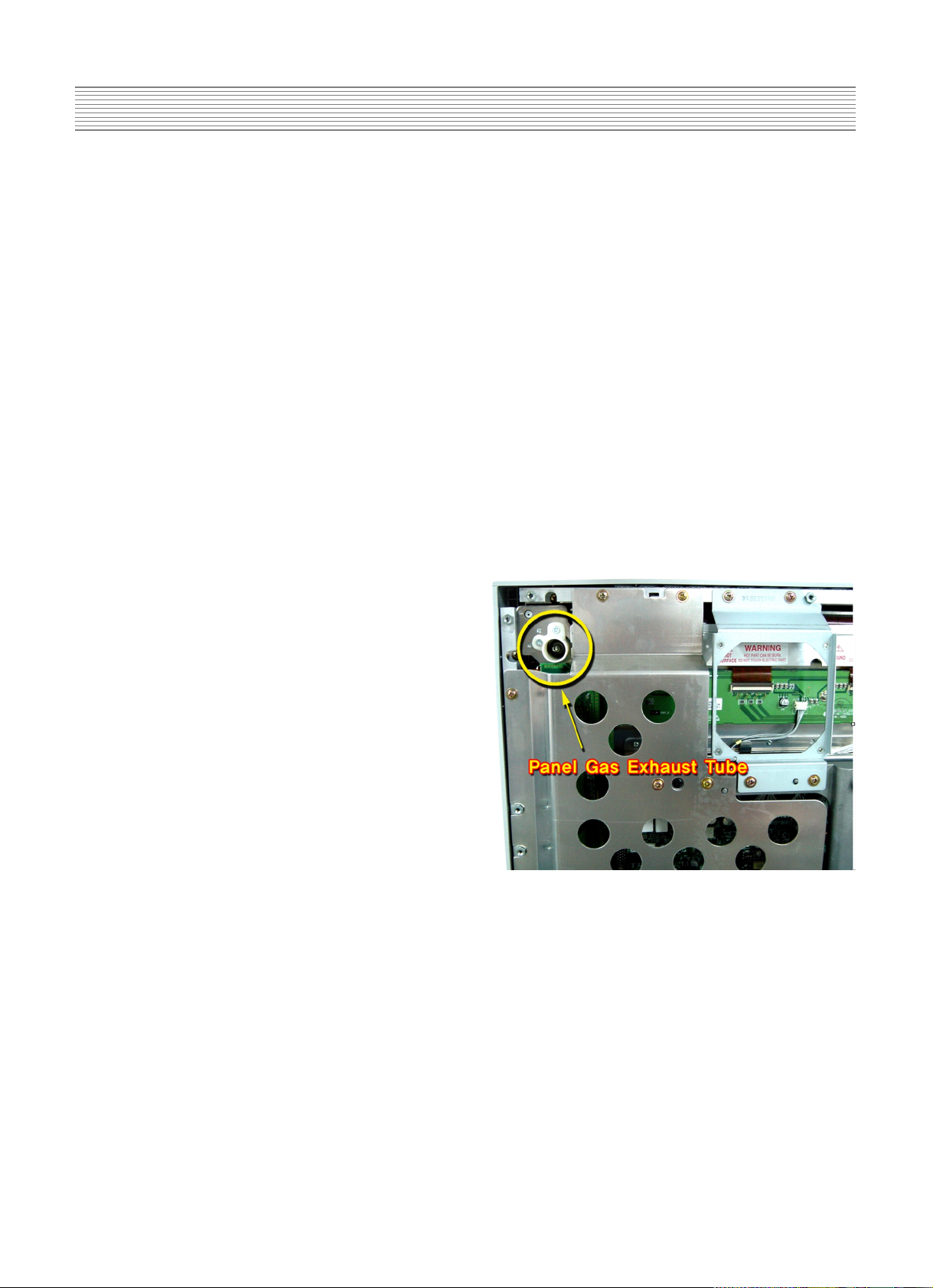
Are you tired of searching the service manuals to look for the value
of a burnt resistor? If the answer is YES, then this eBook is a ‘must
have’ guide for you. You can save a lot of time and be able to repair
customer’s Electronic equipment with burnt resistors in it.
Click here to read more.
Page 2
50” PLASMA PDP MONITOR
CHASSIS : SP-120
MODEL : DSP-5012LXS
S/M NO. : TSP120BEF2
Jan. 2004
Page 3

Contents
A. Parts with the exception of MODULE
1. Safety Precautions
3
2. Product Specification
2-1. SPECIFICATION
4
2-2. Available Input Signal
6
3. BLOCK DIAGRAM
8
4. Description Of Each BLOCK
4-1. A/V BLOCK
9
4-1-1. A/V BLOCK DIAGRAM
9
4-1-2. VIDEO PCB
10
4-1-3. JACK PCB
14
4-1-4. KEY PCB
15
4-1-5. LED PCB
15
4-2. POWER PCB
16
5. SERVICE MODE
5-1. Entering SERVICE MODE
18
5-2. Check initial data of Video PCB
18
5-3. Description Of SERVICE MODE Items
19
6. Adjusting Method
6-1. Adjusting WHITE BALANCE
23
6-2. Adjusting POWER PCB
23
7. SOFTWARE UPGRADE Method
26
8. Main PCB Trouble Diagnosis
29
8-1. VIDEO & JACK PCB Trouble Diagnosis
29
8-2. POWER PCB Trouble Diagnosis
34
9. TROUBLE SHOOTING
9-1. Facts You Must Know When Diagnosing And Repairing
35
9-2. Representative Symptoms When Each PCB Breaks Down
35
9-3. Trouble Diagnosis And Repairing Method For Representative Symptoms
36
10. ASSEMBLY LIST
40
11. EXPLODED VIEW
41
-1-
Page 4

-2-
B. Parts of MODULE
1. Safety Precautions
2
2. Formation and Specification of Module
5
3. Adjustment
6
4. Trouble Shooting
9
5. Block Diagram
14
Page 5
-3-
1. Safety Precautions
A. Parts with the exception of MODULE
1. Safety Precautions
(1) When moving or laying down a PDP Set, at least two people must work. Avoid any impact towards
the PDP Set.
(2) Do not leave the broken PDP Set on for a long time. To prevent any further damages, after check the
condition of the broken Set, make sure to turn the power (AC) off.
(3) When opening the BACK COVER, turn off the power (AC) to prevent electric shock. When a PDP
is on, high voltage and high current exist inside the Set.
(4) When loosening screws, check the connecting position and type of the screw. Sort out the screws
and store them separately. Because screws holding PCB are working as electric circuit
GROUNDING, make sure to check if any screw is missing when assembling.
(5) If you open the BACK COVER, you will see a
Panel Gas Exhaust Tube (Fig. 1). If this part is
damaged, entire PDP PANEL must be replaced.
Therefore, when working, be careful not to
damage this part.
Fig 1. Panel Gas Exhaust Tube
(6) A PDP Set contains a different kind of connector cables. When connecting or disconnecting
connector cables, check the direction and position of the cable beforehand.
(7) When disconnecting connectors, unplug the connectors slowly with care. Especially when
connecting/disconnecting FFC (film) cables or FPC cables, do not unplug the connectors too much
instantaneously or strongly, and always handle the cables with care.
(8) Connectors are designed so that if the number of pins or the direction does not match, connectors
will not fit. When having problem in plugging the connectors, make sure to check their kind,
position, and direction.
Page 6
-4-
2. Product Specification
I T E M S P E C I F I C A T I O N REMARK
1. GENERAL
1-1. MODEL NO DSP-5012LXS
1-2. CHASSIS NO SP-120
1-3. SCREEN SIZE 50”(16:9)
1-4. COUNTRY Europe
1-5. RESOLUTION 1,366(H) X 768(V)
1-6. REMOCON TYPE R-V28A(E)
1-7. SAFETY STANDARD CE(CLASS B), CB
2. MECHANICAL
2-1. APPEARANCE
1) WITHOUT STAND
WxHxD=1,222 x 738 x 93.8 mm
2) WITH STAND
WxHxD=1,222 x 842 x 408 mm
2-2. WEIGHT
1) WITHOUT STAND
48 Kg
2) WITH STAND
55 Kg
3. ELECTRICAL
3-1. VIDEO INPUT COMPOSITE (NTSC, PAL, SECAM, PAL-M/N, NTSC4.43)
& S-
VHS (50/60Hz Y/C) 1 PORTS
SCART(CVBS/RGB) 2ports
3-2. DTV/DVD INPUT 1080i, 720P, 480P , 480i
(Y, Pb/Cb, Pr/Cr, COMPONENT SIGNAL) 2ports
3-3. PC INPUT VGA ~ UXGA (15 PIN D-SUB) 1 PORT
3-4. DVI INPUT DVI-D Input(DVI JACK) 1 port
3-5. SOUND INPUT VIDEO 3ports, DTV/DVD 2 ports,PC 1 port,DVI 1 port
3-6. SPEAKER OUTPUT 8W(R) + 8W(L)
3-7. POWER REQUIREMENT AC 100V~240V, 50/60Hz
3-8. POWER CONSUMPTION 550W
3-9. RS-232 CONTROL RS-232 COMMUNICATION (EXTERNAL UPGRADE)
3-10. FUNCTION
1) SCALING *PC: H/V SIZE AND POSITION ADJUSTMENT
*VIDEO : AUTO, 16:9, PANORAMA, ENLARGE LB, ENLARGE LBS
*DTV/DVD :
AUTO
,16:9
2) ZOOM 20 STEP ZOOM
3) OSD 11 LANGUAGES (ENGLISH, KOREAN, GERMAN, ITALIAN,
DUTCH, PORTUGUESE, SPANISH, MEXICAN, RUSSIAN,
CHINESE, FRANCH)
4) OTHERS STILL, SLEEP MODE , SOUND MODE
2-1. SPECIFICATION
Page 7
-5-
Product Specification
I T E M S P E C I F I C A T I O N REMARK
4. OPTICAL
4-1. SCREEN SIZE 50”(127Cm) DIAGONAL
4-2. ASPECT RATIO 16:9
4-3. NUMBER OF PIXELS
1,366(H)X768(V)
4-4. DISPLAY COLOR
1,677 COLOR( EACH 8BITS FOR RGB )
4-5. CELL PITCH
0.28(H)X0.81(V) Standard for green cell
4-6. PEAK LUMINANCE
360cd/m
2
(With filter glass)
4-7. CONTRAST RATIO
1000:1(Dark Room)
4-8. VIEWING ANGLE
160(VERTICAL/HORIZONTAL)
5. USERCONTROL & ACCESSORIES
5-1 CONTROL BUTTON(SET) AC POWER BUTTON(PUSH-PULL S/W)
MENU, SELECT, UP, DOWN, LEFT, RIGHT(SOFT S/W)
5-2. REMOTE CONTROL
POWER, INPUT SELECT, CONFIRM (or OK),
( R-V28A(E) ) EXTENSION -, EXTENSION +, MENU, UP, DOWN,
VOLUME UP, VOLUME DOWN, SILENCE, PICTURE
MODE, PICTURE STILL, PICTURE SIZE, SOUND
MODE, TIMER SLEEP
5-3. ACCESSORIES
REMOTE CONTROLLER,BATTERY,INSTRUCTION MANUAL,
A/V CABLE, PC CABLE, POWER CORD
OPTION : STAND WALL HANGER, SPEAKER R/L
Page 8
-6-
Product Specification
Resolution H Freq. (KHz) V Freq. (Hz) Remark Patt No.
640x350 31.469 70.1 IBM 203
37.861 85.1 VESA 11
640x400 24.823 56.4 NEC 15
30.48 60.0 PGA 871
31.469 70.1 IBM (DOS) 204
37.861 85.1 VESA 16
640x480 31.469 59.9 DOS 17
35 66.7 Macintosh 18
37.861 72.8 VESA 19
37.5 75.0 VESA 20
39.375 75.0 IBM 21
43.269 85.0 VESA 22
720x400 31.47 60.0 VGA 876
31.469 70.1 IBM 13
37.927 85.1 VESA 14
720X480 31.54 60.0 480P 953
720X576 15.63 25.0 PAL 950
800x600 35.156 56.3 VESA 23
35.16 57.2 VESA 24
37.879 60.3 VESA 24
48.077 72.2 VESA 25
46.875 75.0 VESA 26
53.674 85.1 VESA 27
832x624 49.726 74.0 Macintosh 28
1024x768 48.193(48.077) 59.3(59.8) Macintosh(OAK) 29
48.363 60.0 VESA 30
53.95 66.1 XGA 890
56.476 70.1 HP&VESA 31
60.241 74.9(74.6) Macintosh 32
60.023 75.0 VESA 33
68.677 85.0 VESA 34
80.66 100.0 Fujitsu 939
70.84 84.0 SUN 926
1152X864 54 60.0 VAX 936
63.851 70.0 VESA 35
67.5 75.0 VESA 36
77.094 85.0 VESA 37
1152x900 61.796 66.0 SUN 38
71.713 76.0 SUN 39
1280X720 45 60.0 720P 954
1280X960 60 60.0 VESA 40
75 75.0 VESA 41
85.938 85.0 VESA 42
2-2. Available Input Signal
(1) PC
Page 9
-7-
Product Specification
Resolution H Freq. (KHz) V Freq. (Hz) Remark Patt No.
1280X1024 46.433 43.4 VESA 205
63.981 60.0 VESA 44
70.66 66.5 VAX 937
74.88 70.0 NEC 921
78.125 72.0 HP & HITA 206
78.855 74.1 Sony & NEC 46
79.976 75.0 VESA 47
81.13 76.1 SUN 927
91.146 85.0 VESA 48
1600X1200 62.5 48.0 VESA
75 60.0 VESA 50
81.25 65.0 VESA 862
87.5 70.0 VESA 863
93.75 75.0 VESA 864
100 80.0 VESA 865
(2) DTV
-1080i/ 60 Hz
-720P / 60 Hz
-480P / 60 Hz
(3) VIDEO
-PAL, PAL-M, PAL-N
-NTSC , NTSC4.43
- SECAM
Page 10
-8-
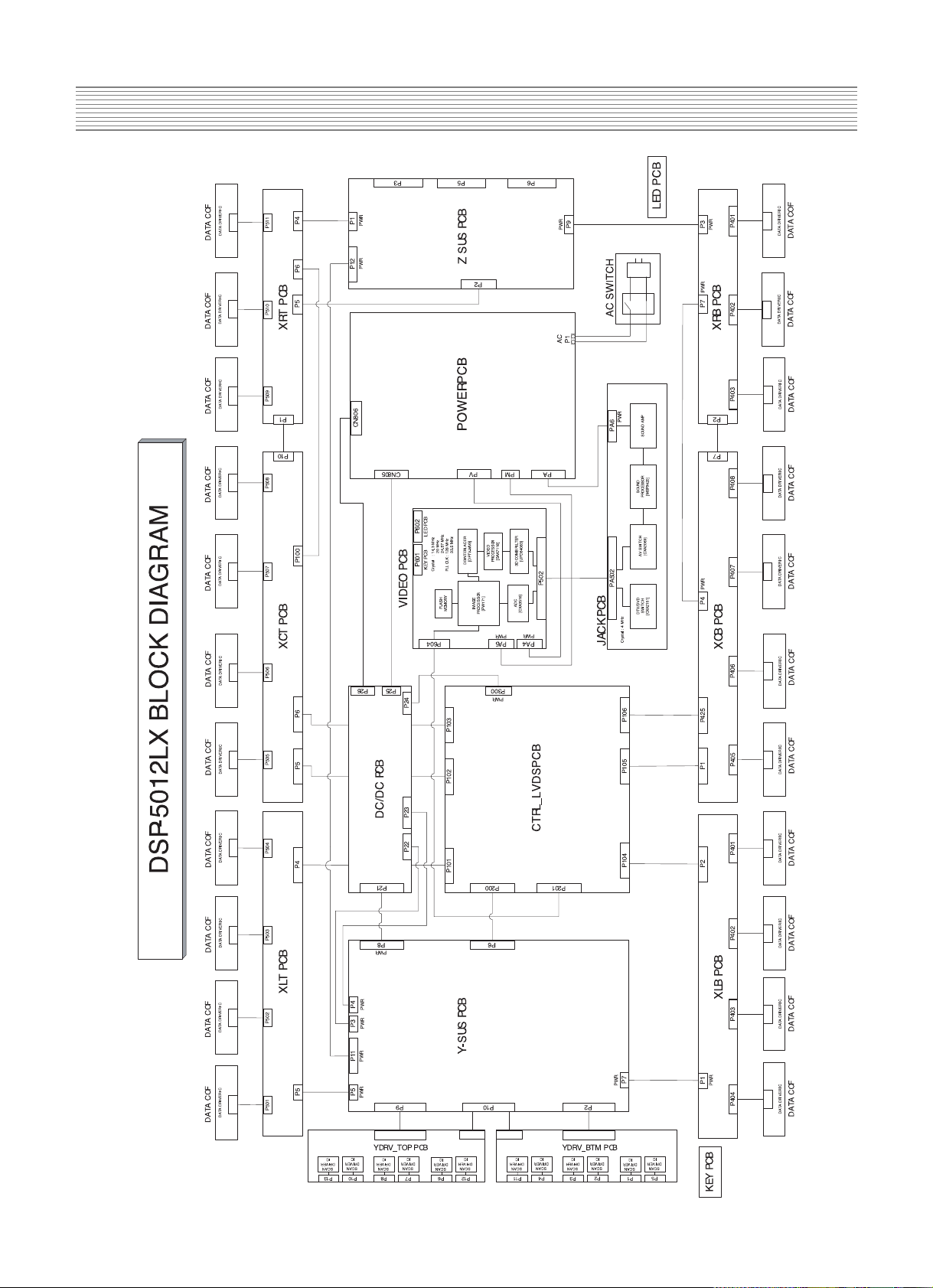
3. BLOCK DIAGRAM
Page 11
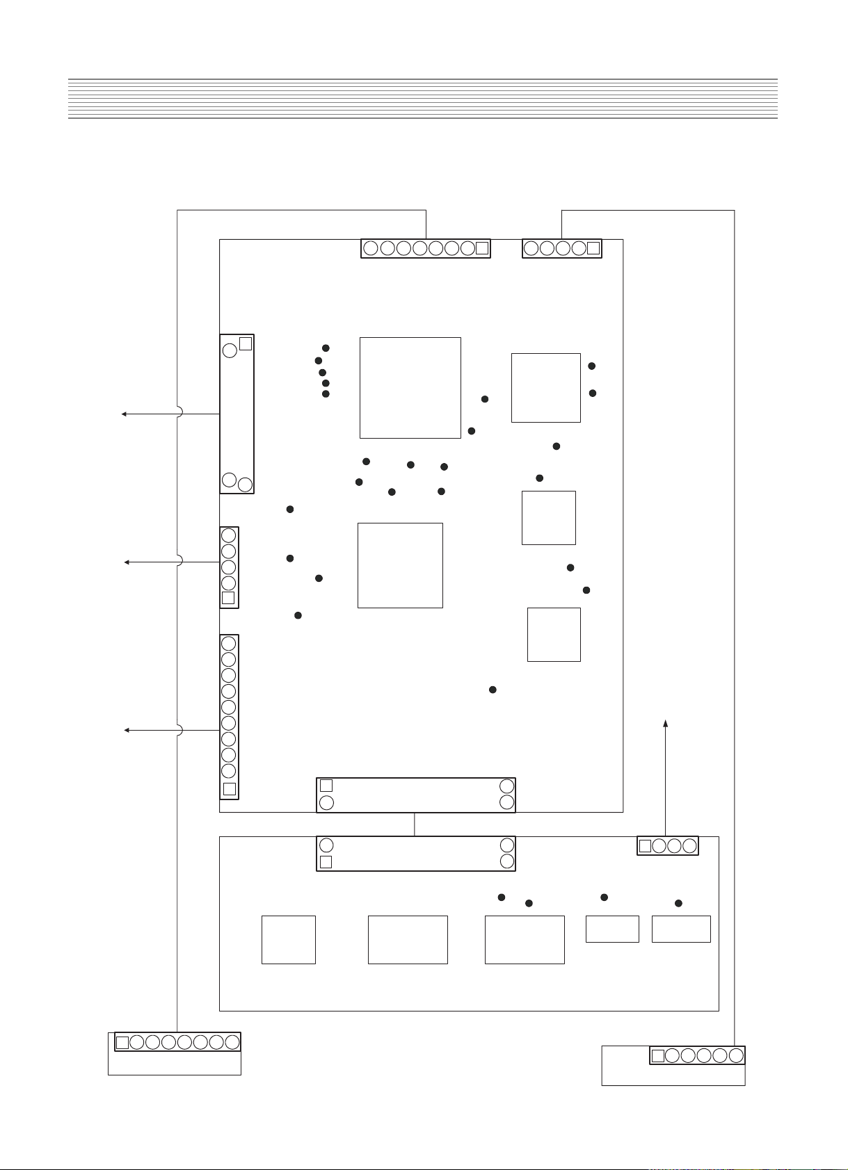
-9-
4. Description Of Each BLOCK
4-1. A/V BLOCK
4-1-1. A/V BLOCK DIAGRAM
to PWR
to PWR
to PWR
to
DIGITAL
P602P601
P12V
P12V
GND
GND
GND
SCL
GND
TXD
RXD
GND
GND
GND
GND
GND
VIN
FB_SC
S_MUTE
MSP_RST
R_SC
G_SC
B_SC
SDA
SEL1
SEL2
SEL3
VPC
HPC
GND
BPC
RPC
GND
GND
B/PB
GND
R/PR
Y_DVDCBCRYOGND
GNDCOGND
GND
GND
GND
G/Y_DTV
GND
GPC
GND
P502
1
50
26
25
1
PA6
1
432
PA502
JACK
PCB
GND
VVS
VHS
VPEN1
GBLKSLP GPEN GSOG
GHSFOUT
DCLKB
DEN
S_RESET
V_MUTE
DVS
DHS
GCLK
GHS
GVS
GCOAST
VIN
R_OUT
L_OUT
RIGHT
LEFT
GREF
VPEN
DECOE
YCOMB
CCOMB
IR
LED_P
GND
GND
GND
E33V
STB5V
COLUM1
COLUM2
COLUM3
DATA1
DATA2
1
5
4
3
2
1
543
2
6
1
40
2
39
PA4
PA5
P603
1
6
7
8
9
5
3
4
2
NUL
P12V
P12V
GND
GND
P5V
GND
GND
LED_P
LED_P
POWER_CLT
GND
GND
GND
GND
GND
GND
RD2-
RD1+
RD1-
RD2-
RD2+
DISPEN
SCLK
GND
RC2-
RB2+
RC2+
RB1-
RB+
RA1-
RB2-
RA2-
RA1+
RC+
RC-
RA2+
RCLK2-
RCLK1+
RCLK2+
RCLK1-
STB5V
SLE
SDATA
STB5V
1
5
2
3
4
IC600
PW171
IC406
DPTV-MVS
IC401
SAA7118
IC400
u64083
IC500
CXA3516
PA602LED
1
5432 6
1
5432
PA601
KEY PCB
IC706
CXA2151
IC704
CXA2069
IC700
MSP3420
IC702
TDA7480
IC701
TDA7480
10
7
8
6 7 8
26
50
25
Page 12
-10-
Description Of Each BLOCK
4-1-2.VIDEO PCB
- PROCESS Various Signal (PC, COMPONENT, COMPOSITE ) to produce 24BIT DIGITAL
output
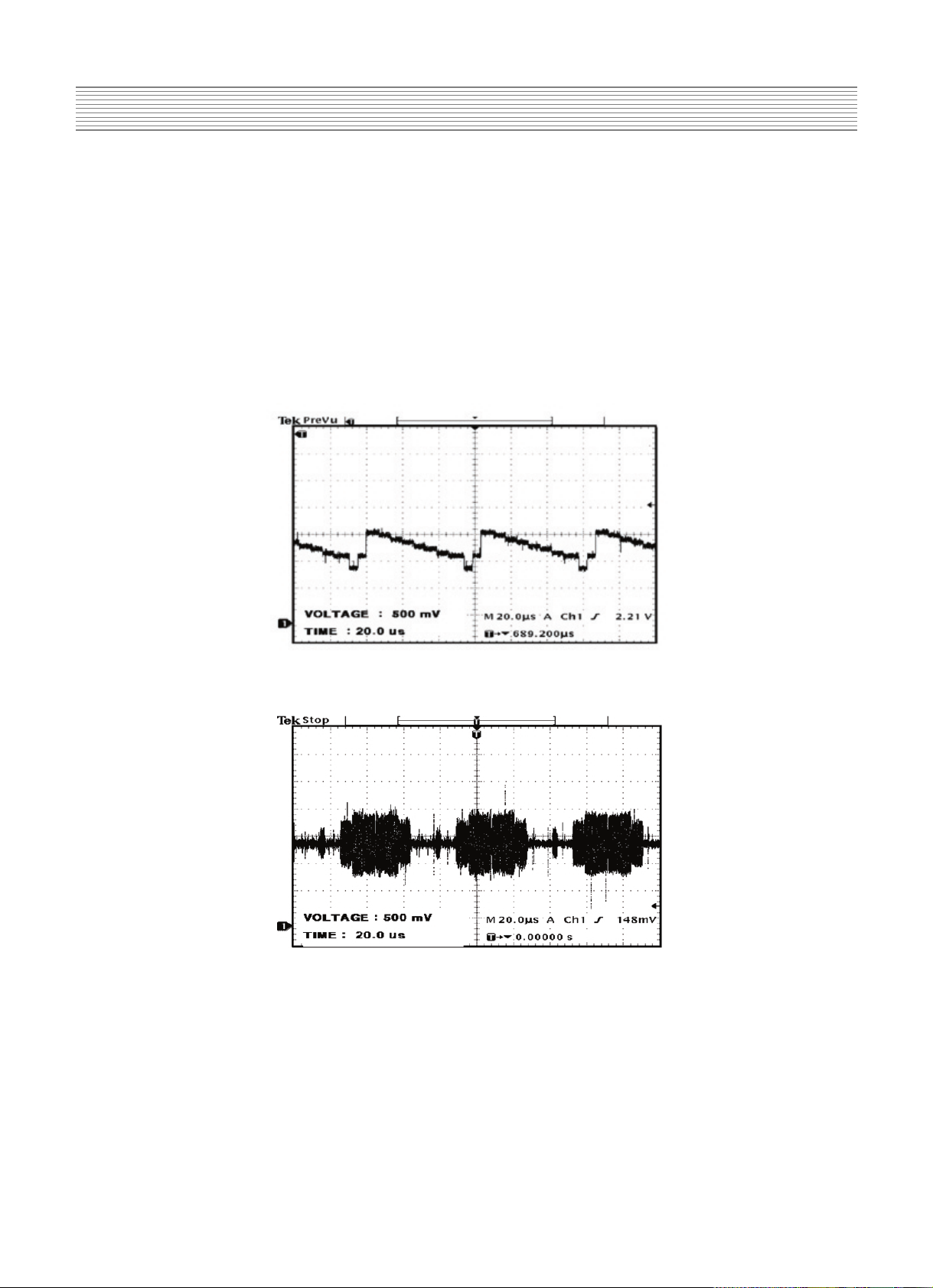
(1) IC and TP
(1) IC400(UPD64083)
-Using 3D COMBFILTER to separate COMPOSITE signal to Brightness
Signal(Y) and Color Signal(C)
*TP ( Input : COLOR BAR PATTERN )
A. YCOMP : Brightness Signal(Y)
B. CCOMP : Color Signal (C)
(2) IC401 (SAA7118E)
-Receive NTSC, SECAM and PAL VIDEO by COMPOSITE(V) , S-VHS(Y.C)
COMPONENT (Y Cb Cr) and process signal
*TP
A. DECOE : CHIP ENABLE part. When signal process is done by IC401, DC 3.3V is
measured.
Page 13
-11-
Description Of Each BLOCK
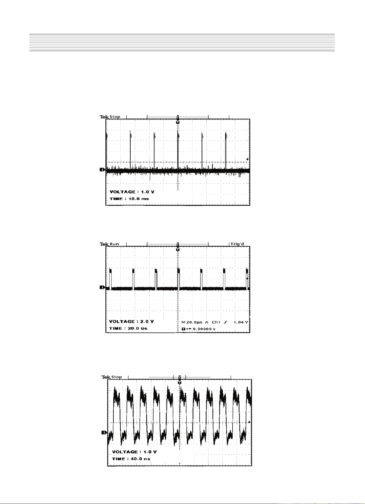
(3) IC406(DPTV-MVS)
-A Scan Rate Converter which converts Interlace signal into Progressive signal
*TP
A. VVS : VERTICAL SYNC (output of DPTV-MVS)
B. VHS : HORIZONTAL SYNC (output of DPTV-MVS)
C. VCLK : CLOCK (output of DPTV-MVS)
Page 14
-12-
Description Of Each BLOCK
(4) IC500(CXA3516R)
-3-channel 8-bit 165MSPS A/D converter which process PC , DTV signal
* TP
A. GCOAST : COAST CONTOL Signal for PLL (input of CXA3516)
B .GHS : HORIZONTAL SYNC for GRAPHIC (output of CXA3516)
C. GCLK : CLOCK for GRAPHIC (output of CXA3516)
Page 15
-13-
Description Of Each BLOCK
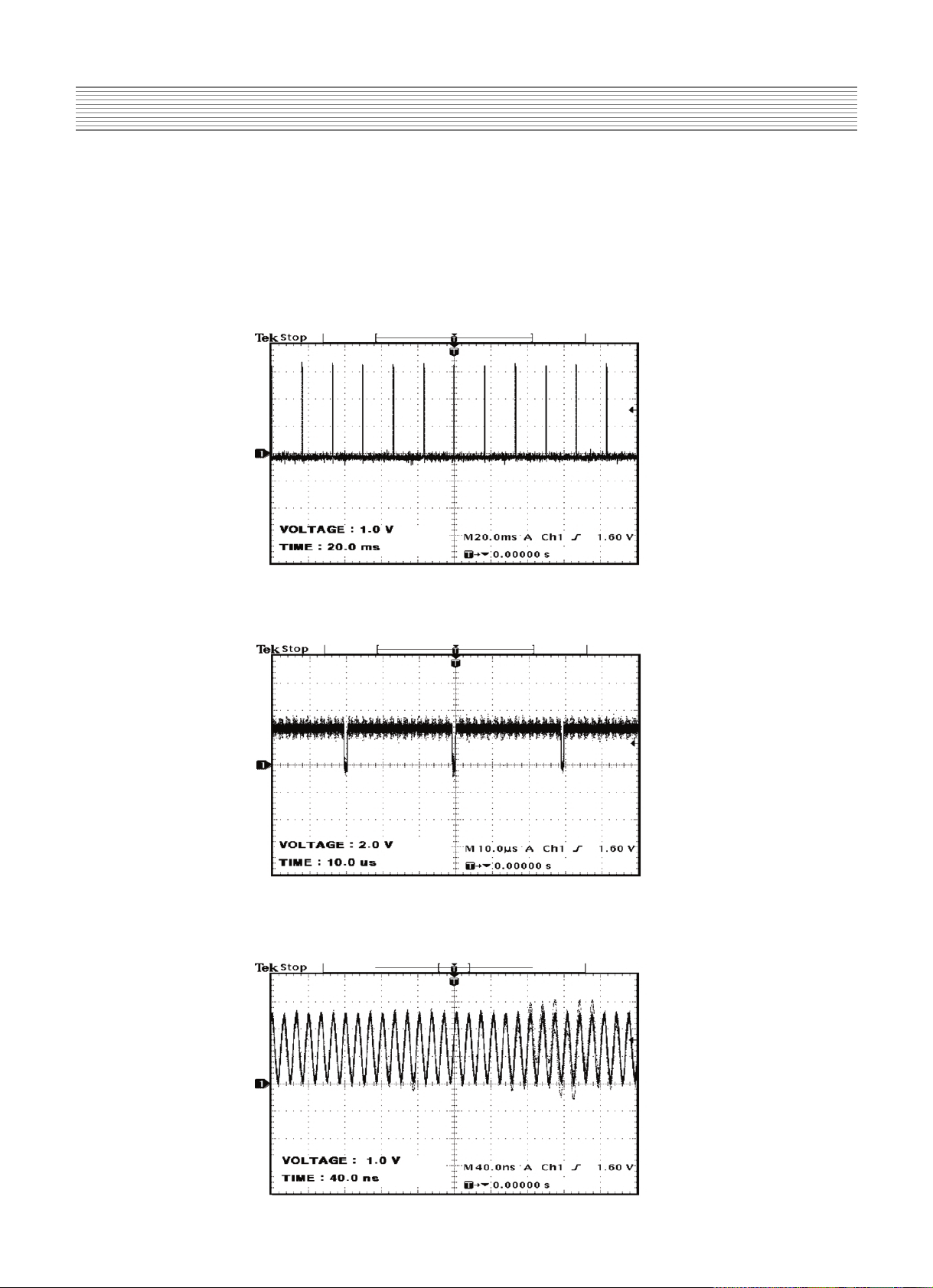
D. GFBK : SYNC for PLL
(5) IC600(PW171)
- Image processor IC
*TP
A. DEN : DATA ENABLE (output of PW171)
B. DHS : HORIZONTAL SYNC (output of PW171)
Page 16
-14-
Description Of Each BLOCK
C.DVS : VERTICAL SYNC for DISPLAY (output of PW171)
D. DCLKB : CLOCK for DISPLAY (output of PW171)
4-1-3. JACK PCB
- Separate and process various VIDEO and AUDIO signal
(1) IC706 (VIDEO /SYNC SELECTOR)
- This chooses Y Cb/Pb Cr/Pr or RGB signal to output Y Cb/Pb Cr/Pr, to separate SYNC,
and to perform SYNC COUNTER.
(2) IC704 (AUDIO/VIDEO SWITCH)
- The IC perform AUDIO or VIDEO SWITCHING
(3) IC715 (DIGITAL CONTROLLER)
- DVI CONTROLLER
(4) IC721 (INPUT SELECTOR SWITCH)
- SCART (RGB) SELECTOR SWITCH
(5) IC700 (MULTI STANDARD SOUND PROCDSSOR)
- AUDIO SINGNAL VOLUME control, EQUALIZER control
Page 17
-15-
Description Of Each BLOCK
*TP
R_OUT(L_OUT) : AUDIO SIGNAL that goes into MSP3420 before AUDIO
PROCESSING
(4) IC701 .IC700 (TDA 7480)
*TP
A. RIGHT(LEFT) :AMP input signal before 30dB amplification
4-1-4.KEY PCB
- Input PCB using KEY
4-1-5.LED PCB
- PCB for REMOCON CONTROL
Page 18
-16-
Description Of Each BLOCK
4-2. POWER PCB
1. Input Specification
1.1 Input condition
3. Output Specification
3.1 Output Voltage & Load Condition
Standard Voltage Range AC 100V ~ 240V
Available Voltage Range AC 85V ~ 276V
Frequency Range 50Hz ~ 60Hz ( 10%)
Item Specification Test Condition
Efficiency 85% Min AC 220V
At Full Load
Inrush Current 40A peak-peak AC 85V ~ 276V
Storage temperature -20 ~ 60
Operation temperature -10 ~ 50 (AMBIENT)
On/Off test temperature -20 ~ 60
Storage humidity 10% ~ 90%
Operation humidity 10% ~ 90%
1.2 Others
2. Environment condition
2.1 Ambient temperature and humidity
No. Output Output Variable Voltage Output 2)*3Ripple &
Name Typical Voltage Tolerance Current(A) Noise (Vp-p)
(V) Range(V) (%) Min. Max.
Vsc Board 1 5V Stand_by 5.0 - 5 0.03 1.0 200/950
(Signal 2 5V 5.2 - 5 0.5 4.5 200/950
Interface) 3 12V 12 - 5 0 1.6 200/850
4
Vaudio
+17 - 5 0 0.7 200/850
5 -17 - 5 0 0.7 200/850
6 33VT 33 - 7 0 0.05 200/850
*1PDP 7 5Vctrl 5.2 - 5 3.0 7.5 200/950
Module 8 Va 60 55~66 1V 0.005 1.6 550/1V
9 Vs 190 10 1V 0.1 2.2 550/1V
Page 19

-17-
Description Of Each BLOCK
4. Input/Output pin assignment & specification
No. Output Output *2Over Current *3Over Voltage Short circuit
Name Typical(V) Protection(A) Protection(V) protection
1
*1
5V 5.0 Short test
stand_by protection
2 5Vctrl 5.2 13.0 or more 5.5~7.0
3 5V 5.2
4 12V 12 1.76 or more 13~17
5 Vaudio +17 1.0 or more 19~24 No hardware
6 -17 1.0 or more -19 ~ -24 failure
7 33VT 33 0.08 or more 36~44
8 Va 60 1.86 ~ 3.30 67 ~80
9 Vs 190 2.42 ~ 4.25 205~230
3.2 Output protection
Page 20

-18-
5. SERVICE MODE
5-1. Entering SERVICE MODE
Push “UP” “MUTE” “DISPLAY” “MUTE” BUTTON of Remote Controller to enter
SERVICE adjustment MODE.
5-2. Check initial data of Video PCB
(1) Check initial data of User Menu
1) Picture
- Mode : Normal
BRIGHTNESS : 35
CONTRAST : 47
COLOR : 32
TINT : 0 (CENTER) * Not displayed when PAL or SECAM input
SHARPNESS : 4
- Color Temp. : Normal
2) Sound
- Balance : 0 (CENTER)
- Spatial Effect : Off
- Sound Mode : Normal
120 Hz : 0 (CENTER)
500 Hz : 0 (CENTER)
1.5 KHz : 0 (CENTER)
5 KHz : 0 (CENTER)
10 KHz : 0 (CENTER)
3) Screen Mode : Normal
4) Utility
- Background : Opaque
- Language : English ( selected when Power ON by user just after manufacturing )
- ISM
Pixel Shift : Off
Low Bright : Off
Image Invert : Off
5) Input
- DSP-4222, DSP-5012:AVI(SCART)
- DSP-4220/24, DSP-5010/14:VIDEO1
(2) Check initial data of Service mode
1) PW 171
- Sub-Brightness : 28
- Sub-Contrast : 40
- Bias R : 60
- Bias G : 60
- Bias B : 68
Page 21

-19-
SERVICE MODE
- Gain R : 70
- Gain G : 70
- Gain B : 64
2) SAA 7118
- Sub BRT : 128
- Sub CONT : 50
- Sub CLR : 55
- Sub TINT : 0
- Sub SRP : 10
3) DPTV
- Sub BRT : 61
- Sub CONT : 16
4) CXA 3516
- Sub CONT : 58
- Cb OFFSET : 39
- Cr OFFSET : 37
- HYS : 3
- THRSLD : 14
5) MSP34X0
- PRESCALE : 22
6) MISC
- AT PWR : OFF
- JACK : Scart(Normal)
- PXL SFT : OFF
7) PANEL
- ISM : OFF
- BWINV : OFF
- GAMMA : 2.2
- BRIGHT : 100 %
- SCROLL : OFF
- P SAVE :100 %
- MOVING : AV
- STILL : AV
5-3. Description of SERVICE MODE Items
1) PW171 : It is a Image processor and used to adjust White balance.
[Note] This article is for adjustment after replacement of VIDEO PCB. These values may vary
from set to set. Therefore if these values are recorded before replacing VIDEO PCB, you do
not need to adjust WHITE BALANCE additionally. The setup can be done using the
recorded values.
Page 22

-20-
SERVICE MODE
(1) SUB BRT : For BRIGHTNESS adjustment (fixed)
(2) SUB CONT : For CONTRAST adjustment (fixed)
(3) BIAS R : For R BIAS adjustment (Changeable)
(4) BIAS G : For G BIAS adjustment (Changeable)
(5) BIAS B : For B BIAS adjustment (fixed)
(6) GAIN R : For R GAIN adjustment (Changeable)
(7) GAIN G : For G GAIN adjustment (Changeable)
(8) GAIN B : For B GAIN adjustment (fixed)
2) SAA7118 : It is a VIDEO DECODER and used to adjust a picture quality for VIDEO/DVD(480i).
[Note] This article is not for adjustment after replacement of VIDEO PCB. Therefore do not
change initial values.
(1) SUB BRT : For BRIGHTNESS adjustment (VIDEO/DVD) (fixed)
(2) SUB CONT : For CONTRAST adjustment (VIDEO/DVD) (fixed)
(3) SUB CLR : For COLOR adjustment (VIDEO) (fixed)
(4) SUB TNT : For TINT adjustment (VIDEO) (fixed)
(5) SUB SRP : For SHARPNESS adjustment (VIDEO) (fixed)
3) DPTV : Be used to adjust DEINTERLACE performance.
[Note] This article is not for adjustment after replacement of VIDEO PCB. Therefore do not
change initial values.
(1) SUB BRT : For BRIGHTNESS adjustment (VIDEO/DVD) (fixed)
(2) SUB CONT : For CONTRAST adjustment (VIDEO/DVD) (fixed)
4) CXA3516 : It is a DTV/PC PROCESSOR and used to adjust a picture quality for DTV/PC.
[Note] This article is not for adjustment after replacement of VIDEO PCB. Therefore do not
change initial values.
(1) SUB CONT : For CONTRAST adjustment (fixed)
(2) Cb OFFSET : For Cb Offset adjustment (fixed)
(3) Cr OFFSET : For Cr Offset adjustment (fixed)
(4) HYS : For Sync hysteresis adjustment (fixed)
(5) THR SLP : For Sync threshold adjustment (fixed)
5) MSP34X0
[Note] This article is not for adjustment after replacement of VIDEO PCB. Therefore do not
change initial values.
(1) PRESCLE : Be used to adjust a Audio prescale.
6) MISC
(1) TST PTRN AT : Cycled patterns from R G B WH every 1 minute automatically.
Page 23

-21-
SERVICE MODE
(2) TST PTRN MA :
Cycled patterns from BK WH R G B by pressing volume up key
(3) AT PWR : ON - Condition where turning AC power on, automatically turns the SET on.
OFF - Condition where turning AC power on makes the Set STAND BY, and POWER of
Remote-controller on turns the set on from STAND BY state.
(4) JACK : Set up depending on input MODE of JACK BOARD
- SCART(Normal) : MULTI + DVI + SCART (DSP-4222LVS, DSP-5012LXS)
- MULTI : Used by DSP-4280 series, Multimedia monitor.
- MONITOR : Used by DSP-4282 series, PC only monitor.
- MONITOR+ : Used by DSP-4282 series with DSP-JU20 attached, PC only monitor with
External board connection.
- DVI : MULTI + DVI, Used by DSP-4284 series, DSP-4220/4224LVS and DSP-5010/5014LXS
- VIDEO : Video only monitor
[Note] Wrong setup causes displaying problem. So you must be careful when SETTING.
(5) PXL SFT : To choose a picture auto shift mode to protect a PDP(Ghost fault)
ON - Moving screen up, down left and right by some Pixels every 20 seconds.
OFF - Fixing PIXEL position. No movement on screen.
[Note] PIXEL SHIFT function is solution to characteristic phenomenon of PDP, so-called
“Image Sticking” problem. Leave this function ON, when displaying many fixed screen
like PC screen. When this function is ON the screen will move a little for every fixed
interval but a human eye can not recognize it well.
7) INFOR
(1) VER : MICOM VERSION
(year 4 digits, month 2 digits, date 2 digits and time 4 digits : 200309222030 )
8) RESET
(1) EDID SET
[Note] Be used to set to write EDID data (After setting it is changed to “EDID DONE”). Before
setting EDID, you have to short jumpers of JP710. After setting, you must remove jumpers,
and then, turn off and on main power. If “EDID WRITING ERROR” is displayed, Try
again. But, in DEUK, you don’t have to set EDID set (After removing jumpers, EDID
DONE is changed to EDID SET).
(2) LEVEL 1 : Be used to initialize all of the data including adjusted figures for W/B.
(3) LEVEL 2 : Be used to initialize all of the data except adjusted figures for W/B
(4) FACTORY : For User menu initialization, is actaviated by choosing a language on AC ON
mode. (Menu Display, VOL, OSD Background and Input mode (VIDEO 1) initialization).
9) PANEL
(1) ISM : Used to minimize Image
Sticking (ON/OFF).
ON : When Still images or regular
patterns have been displayed
on screen for some times, the
luminance of screen is going
to decrease as below. (But,
only when pattern area is over
50% and it is lasting over 5
minutes)
Page 24

-22-
SERVICE MODE
* See the below
(8) MOVING : Setting display mode of Input channel except PC input.
(9) STILL : Setting display mode for PC input.
Table Gamma Contents
1 =2.2(default)
2=1
3 =2.0
4 =2.4
(4) BRIGHT : Adjusting Peak Luminance
1. 100% : Full Peak Luminance
2. 63% : 63% of Peak luminance
3. 40% : 40% of Peak luminance
(* See the graph right)
4. APL: Average Picture Level
(5) SCROLL : Minimizing Image Sticking (ON/OFF) by Shifting whole screen BRIGHT :
Adjusting Peak Luminance. (same with PXL SFT function in 6)MISC)
ON : This function moves1~8 pixel with a regular rule, up, down, left, right every
10 sec
(6) BRIGHT : Adjusting Peak Luminance
(7) P SAVE : Controlling power consumption by changing Luminance level of whole screen.
1. 100% : Peak Luminance & Maximum Power Consumption mode
2. 87% : 87% mode
3. 75% : 75% mode
4. 50% : 50% mode
5. linear : linear mode(Constant luminance without regard to APL)
* WARNING!! The choice of these modes can cause difference of Power Consumption.
(2) BWINV : Used to minimize Image Sticking
(ON/OFF)
ON : Inverting the original images.(in Digital image
data, “0” “1”, “1” “0”)
* If Still images have been displayed for some
periods, this function can minimize Image sticking,
by displaying it on BWINV mode for some times.
(3) GAMMA : can choose one in 4 gamma tables
Page 25

6.Adjusting Method
-23-
6-1. Adjusting WHITE BALANCE
1) Apply 5 Step Gray Scale pattern to Video input terminal
(MIK 7253S PATTERN NO.9)
Fig. 2 5 Step Gray Scale Pattern
2) Check initial data of User Menu ( refer to 5-2 )
3) To enter Service mode, press button “up > mute > recall > mute” on the remote controller and
select PW171, then check initial data of Service mode( refer to 5-2 ).
4) Attach a sensor of White Balance Meter(CA-100) to 80% of white level on the screen.
5) Adjust White Balance by varying Gain of R,G,
* Gain of R, G, should be adjusted to DP+ 10 ,if beyond these then that is a specification fault
* Coordinate of Color is x=0.280 + 0.005, y=0.290 + 0.005 and the Color Temperature is over 10,000-
degree K.
6) Attach a sensor of White Balance Meter to 40% of white level on the screen
7) Adjust White Balance by varying the values of R,G,
* Values of R,G, should be adjusted to DP + 5 ,if beyond these then that is a specification fault
* Coordinate of Color is x=0.280 + 0.005, y=0.290 + 0.005.
8) Repeat No 4) to No 7) until getting that Coordinate of Color is x=0.280, y=0.290, and then adjust
Sub Contrast to over 150 Cd/m square after attaching a sensor of White Balance Meter to 100% of
white level on the screen.
9) To exit from Service mode, press Menu button on the remote controller.
6-2. POWER ADJUSTMENTS
* Video pattern condition : 100 IRE Full White Pattern
* POWER PCB Adjustments mean that you should set the following 2-type power voltages to the
values which were already adjusted by PDP module (LG Module) maker. Therefore, if there are
some problems in picture after adjusting, you should classify that PDP module as a fault and contact
to PDP module maker.
1. Vsus (SUSTAIN Voltage) : Discharge Sustain Voltage
Measurement equipment : Digital Volt Meter ( DC Volt mode )
Adjusting TP : TP3 (See Fig. 4, GND TP:TP2)
Adjusting Location : VR1(See Fig. 4)
Adjusting Voltage : Voltage which is written in Label which is at upper center side of PDP
Module(Vs). (Typical Voltage : 192 V - Fig. 3)
Page 26

-24-
Adjusting Method
Fig. 3 Power Connection and Voltage Adjustment Label
2. Vadd (ADDRESS Voltage) : DATA Input Voltage
Measurement equipment : Digital Volt Meter (DC Volt mode)
Adjusting TP : TP1 (See Fig. 4, GND TP:TP2)
Adjusting Location : VR5 (See Fig. 4)
Optimum Adjusting Voltage : Voltage which is written in Label which is at upper center side of
PDP Module(Va). (Typical Voltage : 60V - Fig. 3)
Page 27

Adjusting Method
-25-
Fig. 4 Power Adjustment Points
Page 28

-26-
7.SOFTWARE UPGRADE Method
1. Connect the JACK PCB to the Video PCB.
2. Connect 9 PIN serial cable to the serial port of the computer.
3. Connect the opposite end of the serial cable to RS-232C port of Jack PCB.
4. Run Flashupgrader.exe in PC and then push “Next(N) >” button.
5. Select current Upgrade file
- Click “Browse” button to select the file you want to upgrade.
Page 29

-27-
SOFTWARE UPGRADE Method
- Select the file (pwSDK.inf) you want to upgrade and Push “Open(O) >” button.
6. Select as above and push “Next(N) >” button.
7. Select Comm Port and Baud Rate and push “Next(N) >” button.
Page 30

-28-
SOFTWARE UPGRADE Method
8. Upgrade process will be displayed. Turn on the ac power and then upgrade program will initiate the
download.
9. When all files upgrade are complete, a window (below) will be opened. Push “Finish” button to
complete the process.
Page 31

-29-
8-1. VIDEO & JACK PCB Trouble Diagnosis
1. Common checking process when “No signal” or “No raster”
2.
When No VIDEO SCART(AV1, AV2), COMPOSITE(AV3), S-VIDEO(AV3), Y Cb Cr) signal on screen
(1) Input PC or DTV signal and see if PC or DTV signals shown on screen.
If no signal, check TP DCLK, DHS and DVS signal.
If DCLK, DHS and DVS signal do not appear, VIDEO PCB has a trouble.
(2) When Y Cb Cr input : Check 16th pin of P502.
8. Main PCB Trouble Diagnosis
Does "No signal" screen
appear?
N
N
Check start
N
N
N
N
N
Y
Y
Y
Y
Y
Y
Y
Y
Is the signal input Jack
correctly connected?
Does input source
(AV device)operate?
Is input selection in used
mode?
Confirm input
selection
Exchange Video or Jack PCB
Check the connection of
Jack(PDP or AV devide)
1. Confirm AC connection
2. Confirm Power S/W ON
3. Check other PCBs
(Refer to B. Parts of Module)
Check P201
Exchange Video PCB
Is P604 correctly
connected?
Is there a weak
discharge on the
screen?
Is DVS, DHS, DCLK of
Video PCB normal?
1. Check other PCBs (CTRL_LVDS,
Y/Z-SUS, CONNECTION PCBs...)
2. Reassemble or change P201
Operate AV device
COMPOSITE Input : Check TP Vin.
[NOTE] See “B. PARTS of MODULE” of this service manual for the trouble diagnosises concerned to
MODULE with exception of VIDEO, JACK and POWER parts.
Page 32

-30-
Main PCB Trouble Diagnosis
(3) TP DECOE Check
If DECOE signal do not appear, JACK PCB has a trouble.
(cf. When COMPOSITE NTSC 3.58MHz, check TP COMB. CCOMB as well)
(4) Check TP VVS, VHS, VCLK and VPEN1
If VVS, VHS, VCLK and VPEN1 signal do not appear, JACK PCB has a trouble.
3. When DTV (1080i, 720P, 480P) signal do not appear on screen
(1) Input PC or VIDEO signal and see if PC or VIDEO signals shown on screen.
If no signal, check TP DCLKB, DHS and DVS.
If DCLKB, DHS and DVS signal do not appear, VIDEO PCB has a trouble.
(2) Check P502’s 1st PIN(V SYNC) , 2nd PIN(H SYNC) check-<when 1080i >
S- VHS input : Check 24th pin of P502 (when COLOR BAR PATTERN).
If above signal do not appear, JACK PCB has a trouble.
If above signals do not appear, JACK PCB has a trouble.
(3) Check TP GHS, GVS and GCLK.
If GHS, GVS and GCLK signal do not appear, JACK PCB has a trouble.
Page 33

-31-
Main PCB Trouble Diagnosis
If above signal do not appear, JACK PCB has a trouble.
(3) Check TP GHS, GVS and GCLK.
If GHS, GVS and GCLK signal do not appear, JACK PCB has a trouble.
5. When No Sound
4. When PC signal do not appear on screen
(1) Input DTV or VIDEO signal and see if DTV or VIDEO signals shown on screen.
If no signal, check TP DCLKB, DHS and DVS.
If DCLKB, DHS and DVS signal do not appear, JACK PCB has a trouble.
(2) Check 1st PIN (V SYNC), 2nd PIN (H SYNC) of P502 (when 800 x 600).
Page 34

-32-
Main PCB Trouble Diagnosis
6. When Key does not operate
N
N
N
Y
Y
Y
Y
Check start
1. Confirm AC connection.
2. Confirm Power S/W ON.
3. Check other PCBs
1. Check the connection to Video PCB.
2. Check the Video PCB or other PCBs.
1. PA601 CONNECTOR has a trouble.
2. Exchange Key PCB.
Does LED
turn on in Green?
Does LED next to Power
S/W turn on in Red?
Is 2nd pin of P601 output normal?
Check VIDEO PCB
Page 35

-33-
Main PCB Trouble Diagnosis
N
N
N
N
Y
Y
Y
Y
Y
Check start
1. Confirm AC connection.
2. Confirm Power S/W ON.
3. Check other PCBs.
Does LED next to Power
S/W turn on in Red?
Check the Battery of
Remote Controller
1. Check the connection to VIDEO PCB
2. Check VIDEO PCB
LED PCB has a trouble.
So, Exchange LED PCB
Does Remote Controller
operate?
Does Set turn on with
Key operation?
1. IR Receiving BLOCK of VIDEO PCB has a trouble.
2. Check VIDEO PCB
Whenever push the botton of
remote controller, does 2nd Pin of
P602 output?
7. When Remote Controller does not operate
Page 36

-34-
Main PCB Trouble Diagnosis
8-2. POWER PCB Trouble Diagnosis
Although Z-SUS / Y-SUS / SCAN / DATA COF (refer to B. PARTS of MODULE) are checked,
but still the set does not operate, and then check if Trouble Symptoms of the following Power PCB
appear.
After unplugging Power Connectors of Z-SUS / Y-SUS PCB(P805A, P806A) and checking
remaining voltage, there still exist several tens of remaining voltage.
When output condition of Power Module is set to low-voltage, output voltage table lists 1~7
are NOT normal. Or when set to high-voltage, output voltage table list 8~9 are NOT normal.
(Refer to 4-2)
When output condition of Power Module is set to low-voltage, output voltage table lists 1~7
are normal. But when set to high-voltage, output voltage table list 1~2 are NOT normal.
(Refer to 4-2)
After turn on the PDP set with Remote Controller, when output condition of Power Module is
set to high-voltage, the LED turn “Green” but the “Power Shut Down” happens after 2~3
seconds.
If high voltage (Vsus, Vadd) measured from Power PCB is different from that of optimum
adjusting voltage label, re-adjust the voltages referring to “A. 6-2. POWER Adjustments”
Page 37

-35-
9. TROUBLE SHOOTING
[NOTE] See “B. PARTS of MODULE” of this service manual for trouble shooting concerned to
MODULE with exception of VIDEO, JACK and POWER parts.
9-1. Facts you must know at trouble diagnosis or repairing
(1) The trouble diagnosis and repairing of set means “Module Exchange”. In other words, find out
which PCB modules are not working and replace them with normal PCB modules. Do not need to
fix broken PCB modules in themselves.
(2) This TROUBLE SHOOTING list only contains representative and simple PCB trouble diagnosis
and Module Exchange method. Therefore, if you find Sets that are difficult to diagnose or to
repair, contact Daewoo Electronics.
(3) Basic TROUBLE SHOOTING procedure
Check Trouble Symptoms Detach BACK COVER Trouble Diagnosis Replace broken
PCB module Adjust new PCB module (when replacing Z-SUS, Y-SUS, POWER,
VIDEO PCB, need Adjusting Procedure. Refer to A.6. Adjusting Method and B.3. Adjustments)
HEATRUN(for at least 30 minutes, input TEST PATTERN FULL WHITE), FUNCTION
CHECK Repair Complete.
(4) Keep broken PCB modules separately for replacing with new PCB modules.
(5) Required equipments for trouble diagnosis
- DIGITAL MULTIMETER (User Mode : measure DC VOLTAGE, measure DIODE VOLTAGE,
SHORT-OPEN TEST )
- Screwdriver (or electric screwdriver), plastic adjusting tool
(6) Each BLOCK operation was explained including DIGITAL OSCILLOSCOPE signal, but this is
reference only and applying them for repair is not necessary. (After additional education, DIGITAL
OSCILLOSCOPE could be used)
(7) Before assemble/disassemble PCBs, check to see if AC Switch is “OFF”.
(8) After replacing Z-SUS, Y-SUS, POWER, VIDEO PCB, the PCB needs extra adjustment. (Refer to
A.6. Adjusting Method and B.3. Adjustments)
(9) After the set is repaired, leave BACK COVER open for followings. Do HEATRUN for at least 30
minutes by inputting TEST PATTERN of SERVICE MODE (Refer to Service Manual A.5. Service
Mode) FULL WHITE. Check the screen conditions and basic functions (remote control operation
etc.).
(10) After BACK COVER is closed, redo HEATRUN for at least one hour by inputting FULL
WHITE using TEST PATTERN of SERVICE MODE. Check the screen conditions and basic
functions.
9-2. Symptoms of VIDEO or JACK PCB Trouble
(1) Symptoms of POWER PCB Trouble
<Symptom.1> Not even weak discharge (luminescence) shows on screen.
<Symptom.2> Discharge (luminescence) on screen is unstable
<Symptom.3> Set is producing unusual noise
<Symptom.4> POWER SHUT DOWN occur (refer to Service Manual A. 9-3)
(2) Symptoms of VIDEO or JACK PCB Trouble
<Symptom.1> Only weak discharge (luminescence) shows on screen, but No Data is on screen
<Symptom.2> Screen DATA is abnormal
<Symptom.3> Particular input signal (Video, PC or Component etc.) does not operate
Page 38

-36-
Trouble shooting
<Symptom.4> No SOUND
<Symptom.5> The Set does not operate normally. But, after turn off AC Power, if turn on again, it
operates normally again.
<Symptom.6> Remote Control or KEY does not operate
<Symptom.7> POWER SHUT DOWN occur (refer to Service Manual A. 9-3 )
(3) Representative Symptoms caused by bad Connection between PCBs.
[Note] Dust or extraneous materials is most likely to cause bad connection. Most of this case, it
can be solved if using soft brush, AIR FRESHER, or breath to clean dust or extraneous
materials or reassembling the Connector.
* Refer to Chapter B for Symptoms of other parts with exception of VIDEO, JACK PCB and POWER
PCB Trouble.
9-3. Trouble Diagnosis and Repairing Method for Representative Symptoms
(1) When POWER SHUT DOWN occurs
<1> Definition of “SHUT DOWN”
- When LED color is green, you can’t hear power operating sound. (Red : STAND BY, Green :
Operating)
- When turn on AC switch and then push “POWER” button of remote controller, power relay do
not operate normally, and POWER operating sound can not be detected.
<2> Trouble Repairing Procedure
- As shown in Fig. 5, first check which of “LOW VOLTAGE” part or “HIGH VOLTAGE” part has
a trouble.
- If “LOW VOLTAGE” part is broken is checked, as shown in Fig. 6 diagnose the SET and then
replace the broken PCB.
- If “HIGH VOLTAGE” part is broken is checked, as shown in Fig. 7 diagnose the SET and then
replace the broken PCB.
- <Note.1> When disconnecting/connecting connectors, you must turn “OFF” the AC power and
check the direction/position of them before working.
- <Note.2> If you turn the SET “ON” with POWER CONNECTORS of Z-SUS PCB and Y-SUS
PCB (P805A, P806A) disconnected, although you turn the SET “OFF” again,
Remaining Voltage still exists in the POWER PCB. Therefore assemble the connectors
several minutes after. Or, check the Remaining Voltage (Vsus, Vadd) by multimeter. If
Vsus is less 10V, connect connectors. Connecting connectors with the Remaining
Voltage (Vsus, Vadd) over 10V could generate sparks and be dangerous to Operators or
SET.
(2) When weak Discharge exists on screen but “OSD” screen” can not be seen
<1> Definition of this symptom
- When the set was turned on, screen is BLACK but Weak Discharge (luminescence) exists.
- When OSD does not show on screen and the set does not respond to remote controller or any
button of KEY panel.
<2> PCB CHECK PRIORITY
- VIDEO PCB
Page 39

-37-
Trouble shooting
<3> Trouble Repairing Procedure
- If no problem in Connection(VIDEO PCB ==>CONTROLLER PCB), replace VIDEO PCB
Fig. 5 Trouble Diagnosis Flow when “SHUT DOWN” occurs
NOYES
AC PWR "OFF"
BACK COVER "OPEN"
AC PWR "ON"
PWR "ON" with Remote Controller
"SHUT DOWN"
occur?
* LOW VOLTAGE part is N.G.
* PCB check priority:
CTRL_LVDS
=> VIDEO => POWER
* Trouble Diagnosis in order shown
as Fig.6
* HIGH VOLTAGE part is N.G.
* PCB check priority:
Z-SUS => Y-SUS => SCAN
=> DATA => POWER
* Trouble Diagnosis in order shown
as Fig.7
POWER PCB’s HIGH VOLTAGE
SWITCH "OFF" (refer to Fig.4)
Page 40

-38-
Trouble shooting
Fig. 6 Trouble Diagnosis Flow when LOW VOLTAGE “SHUT DOWN” occurs
YES NO
YES
NO
YES
NO
AC PWR "OFF"
HIGH VOLTAGE SWITCH of
POWER PCB "OFF" (refer to Fig.4)
Disconnect PWR Connectors of
Z-SUS and Y-SUS(P11, P8, P3, P4)
AC PWR "ON" => PWR "ON" with
Remote Controller
"SHUT DOWN"
occur?
AC PWR "OFF" AC PWR "OFF"
Disconnect PWR
Controller PCB(P300)
Reconnect only PWR Connector
of Y-SUS(P8, P3, P4)
AC PWR "ON" => PWR "ON" with
Remote Controller
AC PWR "ON" => PWR "ON" with
Remote Controller.
"SHUT DOWN"
occur?
"SHUT DOWN"
occur?
VIDEO or JACK
PCB is N.G.
Y-SUS or Y DRV
PCB is N.G.
Z-SUS or
CTRL_LVDS PCB
is N.G.
CTRL_LVDS PCB
is N.G.
Page 41

-39-
Trouble shooting
Fig. 7 Trouble Diagnosis Flow when HIGH VOLTAGE “SHUT DOWN” occurs
AC PWR "OFF"
HIGH VOLTAGE SWITCH of POWER
PCB "ON" (refer to Fig. 4)
Discon
nect PW
R Connectors of
Z-SUS and
Y-SUS(P3, P4, P8, P11)
AC PWR "ON" =>
PWR "ON" with Remote Controller
"SHUT DOWN"
occur?
NO
POWER PCB is N.G.
AC PWR "OFF"
Reconnect only PWR Connector of Y-
SUS (P3, P4, P8)
AC PWR "ON" =>
PWR "ON" with Remote Controller
"SHUT DOWN"
occur?
YES
YES
Z-SUS PCB i s N.G.
NO
Z-SUS or
CTRL_LV DS PCB
is N.G.
Page 42

-40-
10. ASSEMBLY LIST
* Refer to “5. Block Diagram of Module” of Chapter B for connectors (PCN1~PCN11, FCN1~9) of
module parts except above list (18~24).
No. PCB ASS’Y NAME ASS’Y CORD ASS’Y DESCRIPTION
1 VIDEO PCB AS PTVDMSG027 PCB VIDEO MANUAL AS
2 JACK PCB AS PTJMMSG028 PCB JACK MANUAL AS
3 MODULE PDP 4850M06910 PDP50X20340
4 MODULE POWER 4850M06310 PW-1560W
5 CTRL PCB ASS’Y 485AS01790 CTRL PCB AS
6 Y-SUS PCB ASS’Y 485AS01890 Y-SUS PCB AS
7 Z-SUS PCB ASS’Y 485AS01990 Z-SUS PCB AS
8 YDRV-TOP PCB ASS’Y 485AS02090 YDRV-TOP PCB AS
9 YDRV-BTM PCB ASS’Y 485AS02190 YDRV-BTM PCB AS
10 XCT PCB ASS’Y 485AS02290 XCT PCB AS
11 XCB PCB ASS’Y 485AS02390 XCB PCB AS
12 XLT PCB ASS’Y 485AS02490 XLT PCB AS
13 XLB PCB ASS’Y 485AS02590 XLB PCB AS
14 XRT PCB ASS’Y 485AS02690 XRT PCB AS
15 XRB PCB ASS’Y 485AS02790 XRB PCB AS
16 DC-DC PCB ASS’Y 485AS02890 DC-DC PCB AS
17 PANEL GLASS 485AS01696 PANEL GLASS AS
18 CONNECTOR 4850710025 YMH025-10+YMT025+ULW=600
19 CONNECTOR 4850705S16 YMH025-05R+YMH025-05R+ULW=600
20 CONNECTOR 4850708S10 12505HS-08+12505HS-08+ULW=900
21 CONNECTOR 4850705N26 12505HS-05+12505TS+ULW=1100
22 CONNECTOR 4850706S25 YMH025-06R+YMH025-06R+ULW=300
23 CONNECTOR 4850704S47 GP390-04S+GP390-04S+ULW=200
24 CONNECTOR 4850710S05 GP390-10S+GP390-10S+ULW=200
25 CABLE LVDS AS 4859001660 GT121-31S+5010LX=450
26 BACK COVER 4851413300 DSP-5010LXS
27 FILTER GLASS 485A100480 PDF-96H04
Page 43

-41-
Page 44

- 2 -
PDP Module is a display device to be divided into a Panel part
and a Drive part. The Panel part consists of
Electrodes, Phosphor, various dielectrics and gas, and the Drive
part includes electronic circuitry and PCB.
When using/handling this PDP Module, pay attention to the
below warning and cautions.
Warning?
Indicates a hazard that may lead to death or injury if the
warning is ignored and the product is handled incorrectly.
Caution?
Indicates a hazard that can lead to injury or damage to
property if the caution is ignored and the product is handled
incorrectly.
¥.WARNING
(1) Do not supply a voltage higher than that specified to this
product. This may damage the product and may cause a
fire.
(2) Do not use this product in locations where the humidity is
extremely high, where it may be splashed with water, or
where flammable materials surround it.
Do not install or use the product in a location that does no
satisfy the specified environmental conditions. This may
damage the product and may cause a fire.
(3) If a foreign substance (such as water, metal, or liquid) gets
inside the product, immediately turn off the power.
Continuing to use the product, it is may cause fire or
electric shock.
(4) If the product emits smoke, and abnormal smell, or makes
an abnormal sound, immediately turn off the power.
Continuing to use the product, it may cause fire or electric
shock.
(5) Do not disconnect or connect the connector while power to
the product is on. It takes some time for the voltage to drop
to a sufficiently low level after the power has been turned
off.
Confirm that the voltage has dropped to a safe level before
disconnecting or connecting the connector.
(6) Do not pull out or insert the power cable from/to an outlet
with wet hands. It may cause electric shock.
(7) Do not damage or modify the power cable. It may cause
fire or electric shock.
(8) If the power cable is damaged, or if the connector is loose,
do not use the product: otherwise, this can lead to fire or
electric shock.
(9) If the power connector or the connector of the power cable
becomes dirty or dusty, wipe it with a dry cloth. Otherwise,
this can lead to fire.
(10) PDP Module uses a high voltage (Max.450V dc). Keep
the cautions concerning electric shock and do not touch
the Device circuitry when handling the PDP Unit. And
because the capacitor of the Device circuitry may remain
charged at the moment of Power OFF, standing by for 1
minute is required in order to touch the Device circuitry.
¥–.CAUTIONS
(1) Do not place this product in a location that is subject to
heavy vibration, or on an unstable surface such as an
inclined surface. The product may fall off or fall over,
causing injuries.
(2) Before disconnecting cable from the product, be sure to
turn off the power. Be sure to hold the connector when
disconnecting cables. Pulling a cable with excessive force
may cause the core of the cable to be exposed or break
the cable, and this can lead to fire or electric shock.
(3) This product should be moved by two or more persons. If
one person attempts to carry this product alone, he/she
may be injured.
(4) This product contains glass. The glass may break, causing
injuries, if shock, vibration, heat, or distortion is applied to
the product.
(5) The temperature of the glass of the display may rise to
80°C or more depending on the conditions of use.
If you touch the glass inadvertently, you may be burned.
(6) If glass surface of the display breaks or is scratched, do
not touch the broken pieces or the scratches with bare
hands. You may be injured.
(7) PDP Module requires to be handled with care not to be
touched with metal or hard materials, and must not be
stressed by heat or mechanical impact.
(8) There are some exposed components on the rear panel of
this product. Touching these components may cause an
electric shock.
(9) When moving the product, be sure to turn off the power
and disconnect all the cables. While moving the product,
watch your step. The product may be dropped or all,
leading to injuries of electric shock.
SAFETY PRECAUTIONS
Page 45

English
(10) In order to protect static electricity due to C-MOS circuitry of
the Drive part, wear a wrist band to protect static electricity
when handling.
(11) If cleaning the Panel, wipe it with a soft cloth moistened with
water or a neutral detergent and squeezed, being careful not
to touch the connector part of the Panel. And don’t use
chemical materials like thinner or benzene.
(12) If this product is used as a display board to display a static
image, “image sticking” occurs. This means that the luminance
of areas of the display that remain lit for a long time drops
compared with luminance of areas that are lit for a shorter
time, causing uneven luminance across the display.
The degree to which this occurs is in proportion to the
luminance at which the display is used. To prevent this
phenomenon, therefore, avoid static images as much as
possible and design your system so that it is used at a low
luminance, by reducing signal level difference between bright
area and less bright area through signal processing.
(13) Because PDP Module emits heat from the Glass Panel part
and the Drive circuitry, the environmental temperature must
not be over 40°C.
The temperature of the Glass Panel part is especially high
owing to heat from internal Drive circuitry. And because the
PDP Module is driven by high voltage, it must avoid
conductive materials.
(14) If inserting components or circuit board in order to repair, be
sure to fix a lead line to the connector before soldering.
(15) If inserting high-power resistor(metal-oxide film resistor or
metal film resistor) in order to repair, insert it as 10mm away
as from a board.
(16) During repairs, high voltage or high temperature components
must be put away from a lead line.
(17) This is a Cold Chassis but you had better use a cold
transformer for safety during repairs. If repairing electricity
source part, you must use the cold transformer.
(18) Do not place an object on the glass surface of the display.
The glass may break or be scratched.
(19) This product may be damaged if it is subject to excessive
stresses (such as excessive voltage, current, or temperature).
The absolute maximum ratings specify the limits of these
stresses.
(20) The recommended operating conditions are conditions in
which the normal operation of this product is guaranteed. All
the rated values of the electrical specifications are guaranteed
within these conditions.
Always use the product within the range of the recommended
operating conditions. Otherwise, the reliability of the product
may be degraded.
(21) This product has a glass display surface. Design your
system so that excessive shock and load are not applied to
the glass. Exercise care that the vent at the corner of the glass
panel is not damaged.
If the glass panel or vent is damaged, the product is
inoperable.
(22) Do not cover or wrap the product with a cloth or other
covering while power is supplied to the product.
(23) Before turning on power to the product, check the wiring of
the product and confirm that the supply voltage is within the
rated voltage range. If the wiring is wrong or if a voltage
outside the rated range is applied, the product may
malfunction or be damaged.
(24) Do not store this product in a location where temperature
and humidity are high. This may cause the product to
malfunction. Because this product uses a discharge
phenomenon, it may take time to light (operation may be
delayed) when the product is used after it has been stored for
a long time. In this case, it is recommended to light all cells for
about 2 hours (aging).
(25) This product is made from various materials such as glass,
metal, and plastic. When discarding it, be sure to contact a
professional waste disposal operator.
(26) If faults occur due to arbitrary modification or disassembly,
LG Electronics is not responsible for function, quality or other
items.
(27) Use of the product with a combination of parameters,
conditions, or logic not specified in the specifications of this
product is not guaranteed. If intending to use the product in
such a way, be sure to consult LGE in advance.
(28) Within the warranty period, general faults that occur due to
defects in components such as ICs will be rectified by LGE
without charge. However, IMAGE STICKING due to
misapplying the above (12) provision is not included in the
warranty. Repairs due to the other faults may be charged for
depending on responsibility for the faults.
- 3 -
Page 46

English
¥ . Formation and Specification of Module
- 5 -
External Cable Connection
NO
1
2
3
4
5
6
7
8
9
10
11
12
13
14
Part No.
6871QCH028A
6871QCH033A
6871QDH048A
6871QDH049A
6871QLH032A
6871QLH033A
6871QXH020A
6871QXH021A
6871QRH035A
6871QRH036A
6871QYH028A
6871QZH031A
6871QEH017A
6871QPH008A
PWB(PCB) ASSY
PWB(PCB) ASSY
PWB(PCB) ASSY
PWB(PCB) ASSY
PWB(PCB) ASSY
PWB(PCB) ASSY
PWB(PCB) ASSY
PWB(PCB) ASSY
PWB(PCB) ASSY
PWB(PCB) ASSY
PWB(PCB) ASSY
PWB(PCB) ASSY
PWB(PCB) ASSY
PWB(PCB) ASSY
Description
TMDS CTRL B/D ASSY
LVDS CTRL B/D ASSY
Y DRV UPPER B/D ASSY
Y DRV LOWER B/D ASSY
X LEFT TOP B/D ASSY
X LEFT BOTTOM B/D ASSY
X CENTER TOP B/D ASSY
X CENTER BOTTOM B/D ASSY
X RIGHT TOP B/D ASSY
X RIGHT BOTTOM B/D ASSY
Y SUS B/D ASSY
Z SUS B/D ASSY
T/C B/D ASSY
DC/DC B/D ASSY
NO
1
2
3
Connector
P25[DC_DC B/D]
P26[DC_DC B/D]
P100, P201[CTRL B/D]
Input Signal
5V
Va, Vs
TMDS, LVDS Video Signal input
Page 47

- 6 -
1. Application Object
This standard is applied to the PDP50X2#### PDP Module
which is manufactured by the manufacturing team of PDP
promotion department or elsewhere.
2. Adjustment items & Notes
2-1. Adjusting the Board Group
(1) Adjusting the voltage wave form of Vset-up
(2) Adjusting the voltage wave form of Vset-down
(3) Adjusting the voltage wave form of Vzb
2-2. Adjustment after assembling
(PDP Module adjustment)
(1) Adjusting the initial voltage wave form
(2) Measuring the voltage Margin of Vs and deciding the
voltage
(3) Measuring the voltage Margin of Vset-up and deciding the
voltage
(4) Adjusting the wave form of final voltage
(5) Module Aging
2-3. Notes
(1) Adjustment must be done in the correct order.
But, these items above can be changed by the
consideration of mass production. (When changing the
sequence, there should be an agreement of the Module
development / QA / Manufacturing)
(2) Without any special specification, you should adjust the
Module in the environment of Temp (25
!5°C) and Relative
humidity (65!10%)
(3) If you let the still image more than 10 minutes(especially
The Digital pattern or Cross Hatch Pattern which has clear
gradation), image can be presented in the black level part of
screen.
3. Adjusting the Board Group
3-1. Using Tools
(1) Oscilloscope : 1EA
(2) DMM : 1EA
(3) Signal generator : VG-825 or similar one
(4) DC power supply
- DC power supply for Vs (1) : Should be changeable more
than 0-200V/ more than 10A
- DC power supply for Va (1) : Should be changeable more
than 0-100V/ more than 5A
- DC power supply for 5V (1) :Should be changeable more
than 0-10V/ more than 10A
3-2. Signal & Power feed
(1) Connect measuring instrument like the connection diagram
Fig. 1.
(2) Turn on the power of the measuring instrument like the
<Caution> item Fig. 1.
3-3. How to Adjust
(1) Adjusting the Voltage Wave form of Vset-up
¤ Connect the oscilloscope probe to B41(SUS_UP) and
GND of Y-SUS PCB.
¤Ł Turn the VR1 of Y-SUS PCB and make the “A“ wave
form Fig. 2 to be 50!1µs.
(2) Adjusting Vset-down Voltage Wave form
Turn the VR2 of Y-SUS PCB and make the “B” wave form
Fig. 2 to be 120!5µs.
(3) Adjusting Vzb Voltage Wave form
¤ Connect oscilloscope Probe to the B39 and GND of Z-
SUS PCB.
¤ŁTurn the VR1 of Z PCB and make the “C” wave form Fig.
3 to be 10!0.5V.
¥–. Adjustment
Vsc Voltage
(90 ~120V)
0V
Vs Voltage
(180~ 195V)
Vsetup Voltage
(230~260 V)
140µs
50µs±1µs
120µs±5µs
- Vy Voltage
(- 40 ~ - 90V)
(Fig. 2) Y SUSTAIN Voltage Wave from
Ramp Erase Pulse
(Adjustment not requirement)
C (10±0.5V)
0V
Vzb Voltage
Vs Voltage
(180~ 195V)
(Fig. 3) Z SUSTAIN Voltage Wave from
Page 48

English
- 7 -
4. Adjustment after Assembling
(PDP Module Adjustment)
4-1. Using Tools
(1) Oscilloscope : 1EA
(2) DMM : 1EA
(3) Signal generator : VG-825 or similar one
(4) DC power supply
- DC power supply for Vs (1) : Should be changeable more
than 0-200V/ more than 10A
- DC power supply for Va (1) : Should be changeable more
than 0-100V/ more than 5A
- DC power supply for 5V (1) : Should be changeable more
than 0-10V/ more than 10A
4-2. Connection diagram of measuring
instrument
Connection diagram of measuring instrument
Refer to figure 1. (Connection diagram of measuring
instrument)
4-3. How to Adjust
(1) Adjusting initial voltage wave form
Check the voltage wave form like the mentioned way on
the 3-3(How to adjust) and readjust the wave form when it
is wrong.
(2) Measuring the Vs voltage Margin and deciding
the voltage
¤ Convert the signal of signal generator to the 100% Full
RED signal.
¤ŁTurn the voltage adjusting knob of Vs DC power supply
to the voltage -down direction and make the cell of
screen turned off.
¤Ø Turn the voltage adjusting knob of Vs DC power supply
to the voltage -up direction until the cell of screen turned
on.
The first voltage, which make the cell of full screen
turned on, is named as Vsmin1 and record it.
¤Œ Turn the voltage adjusting knob of Vs DC power supply
to the voltage-up direction slowly until the cell of screen
turned off or over electric discharge.
The first voltage, which makes the cell of screen turned
off or over electric discharge, is named as Vsmax1 and
records it. (but, Vs voltage shouldn’t exceed 195V)
¤º Convert the signal of signal generator to the 100% Full
Green signal.
¤ Repeat the adjustment from ¤Ł to ¤Œ and name each
voltage as Vsmin2/Vsmax2 and record them.
¤ Convert the signal of signal generator to 100% Full Blue
signal.
¤ Repeat the adjustment from ¤Ł to ¤Œ and name each
voltage as Vsmin3/Vsmax3 and record them.
¤ Convert the signal of signal generator to 100% Full
White signal.
¤ Repeat the adjustment from ¤Ł to ¤Œ and name each
voltage as Vsmin4/Vsmax4 and record them.
¤æ Convert the signal of signal generator to 100% Full
Black signal.
¤ Repeat the adjustment from ¤Ł to ¤Œ and name each
voltage as Vsmin5/Vsmax5 and record them.
¤ At this time decided Vs voltage (Vsmin1-Vsmin5)adds 4V to
Max value and set up the voltage within the set-up
range(180V
# Vs # 195V) in consideration of other
features.
¤ Turn the voltage adjusting knob of Vs DC power supply
make deciding the Vs voltage.
(3) Measuring the Vset-up voltage and deciding
voltage
¤ Convert the signal of signal generator to FULL WHITE 88
Gray.
¤Ł Turn the variable resistor of Vsetup in DC/DC Board to the
lower minimum voltage(230V).
¤Ø After FULL WHITE 88 Gray Pattern permission, turn the
variable resistor of Vsetup in DC/DC Board to the voltagedown direction and record the minimum voltage(Vset-up
min) which has mis-electric discharge or elimination when
examining with eyes at a distance of 50cm.
¤Œ After FULL WHITE 64 Gray Pattern permission, turn the
variable resistor of Vsetup in DC/DC Board to the voltagedown direction and record the maximum voltage(Vset-up
max) which has mis-electric discharge when examining
with eyes at a distance of 50cm.
(but, Vset-up voltage shouldn’t exceed 260V)
Vset-up Margin = it is decided with (Vset-up max - Vset-up min)
Deciding voltage of Vset-up is decided by the middle value
of Margin in the voltage range 230~260V.
¤º Turn the variable resistor of Vsetup in DC/DC Board and
set up as the deciding Vset-up voltage.
(4) Adjusting the final voltage wave form
Check the voltage wave form like the mentioned way on the 33(How to adjust) and readjust the wave form when it is twisted.
[ The C wave form of Vzb voltage considers an other quality and
5~15V it will be able to adjust from inside scope
(5) DC-DC Pack Voltage Set up Range
Vsetup : 230V ~ 260V
Vsc : 90V ~ 120V
-Vy : -40V ~ -90V
-Ve : -Vy + 10V ~ -Vy + 34V
5. Module Aging
Module should get the Aging for the equilibrium after finish the
assembling. Aging condition is shown below.
(1) Service signal: 100% Full White, Red, Green, Blue, Cyan,
Magenta, Yellow pattern, 16 Gray more than Pattern, 50%
Full White Pattern, each Pattern signal...(Service time of each
pattern : within 5minutes/cycle)
(2) Service DC power voltage : Vs:190V, Va:60V, -Vy:-55V,
-Ve:-30V, Vset-up:250V, Vsc:100V, Vzb:180V
(Voltage gap !0.5V, Adjust the voltage of -Vy, -Ve, Vsetup, Vsc to variable resistor of DC/DC Board.)
--> Refer to Fig. 1.
(3) Aging time : More than 4Hrs
(4) Aging environment: Temp (50°C), Relative humidity (65%)
Page 49

- 8 -
(Fig. 1) Connection diagram of measuring instrument
<Caution>
(1) The power of the signal generator should be turned on before turning on the power of DC power supply.
(2) The voltage of DC power supply , in standard of Module input voltage, should be preset as below.
Vs : 192V, Va : 60V
(3) The power of power supply must turned on by this sequence. Reverse direction When turning off.
* Module on : 5V
(Vs(
Va, Module off : Va(Vs(5V
(4) Signal generator should be selected with 1366x768 mode.
Page 50

English
- 9 -
1. Checking for no Picture
A screen doesn¡flt display at all and condition of black pattern or power off.
(1) Check whether the CTRL B/D LED(D1) is turned on or not.
(2) Check the power and signal cable of CTRL B/D.
(3) X B/D, Y B/D, Z B/D is well plugged in.
(4) Check the connection of X B/D, Y B/D and Z B/D to CTRL B/D.
(5) Measure the output wave of Y, Z B/D with oscilloscope(more than 200MHz)
and find the trouble of B/D by comparing the output wave with below figure.
- Measure Point fo Y B/D : TP (B41)
- Measure Point fo Z B/D : TP (B39)
(6) Check the SCAN(Y side) IC
(7) Check the DATA(X side) COF IC
(8) Replace the CTRL B/D.
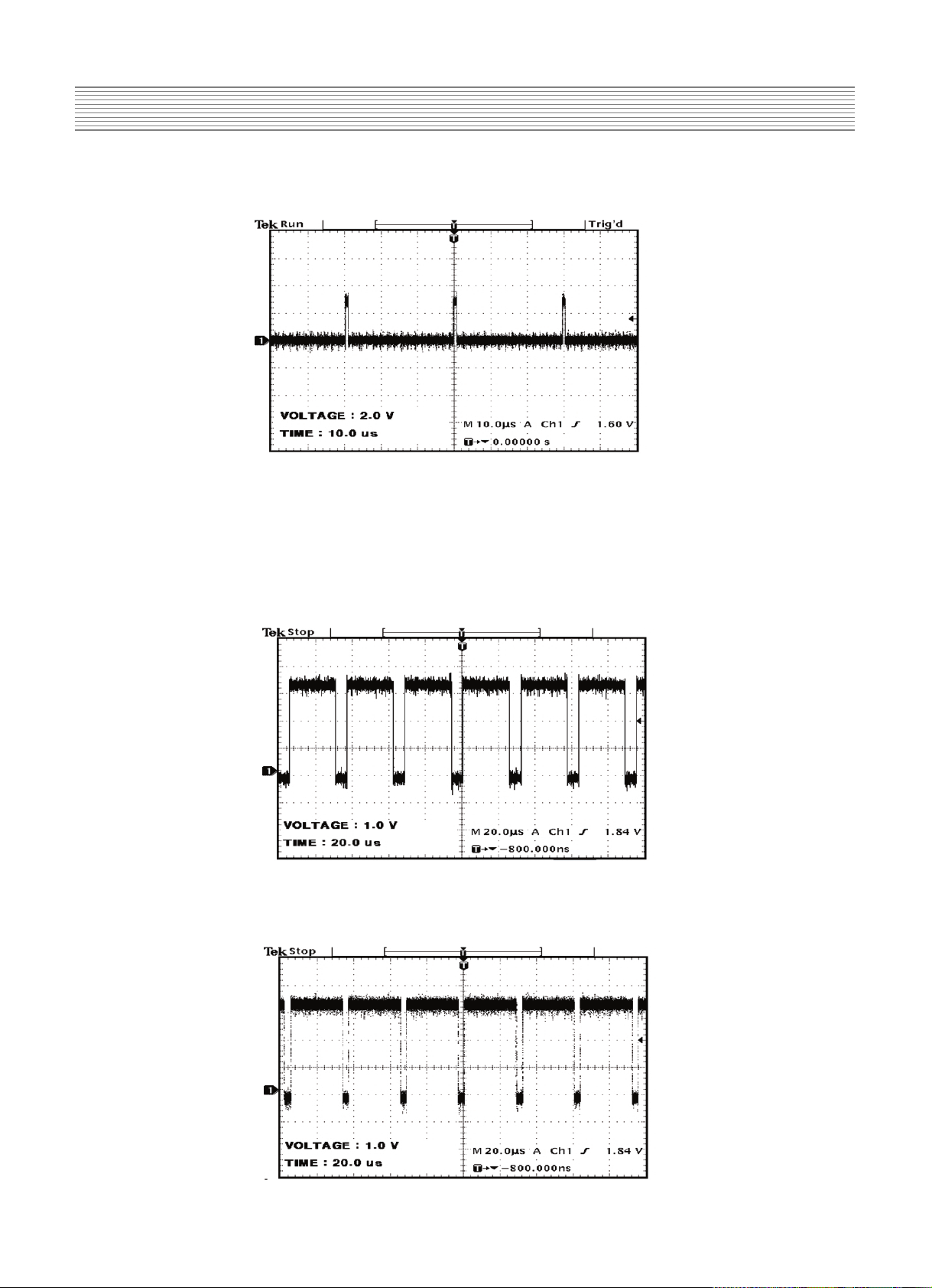
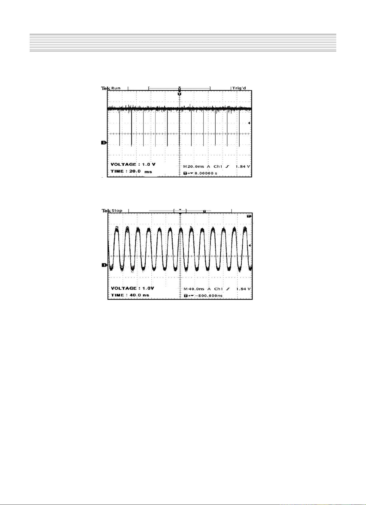
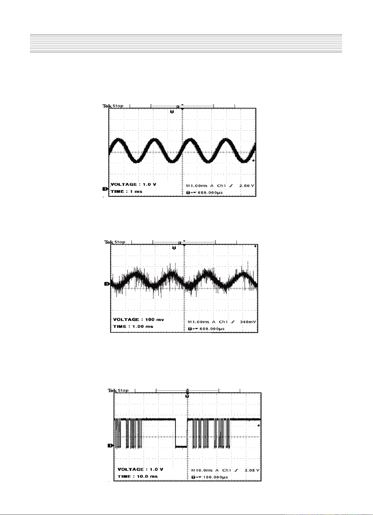
<Y B/D Output wave - 1FRAME>
<Z B/D Output wave - 1FRAME>
<Y B/D Output wave Enlargement - 1 SF>
<Z B/D Output wave Enlargement - 1 SF>
<Y B/D Output wave Enlargement - 7~12 SF>
¥†. Trouble Shooting
Page 51

- 10 -
2. Hitch Diagnosis Following
Display Condition
2-1. 3/11 or 4/11 of the screen doesn’t be
shown
(1) Confirm the power connector of X B/D is well plugged in
which is correspond to not showing screen.
(2) Confirm the connector that is connected between CTRL
B/D and X B/D correspond to not showing part.
(3) Replace relevant X B/D.
[[
Relationship between screen and X B/D
Screen X B/D
Top Left of the Screen 3/11 <--> X Right Top B/D
Top Center of the Screen 4/11 <--> X Center Top B/D
Top Right of the Screen 4/11 <--> X Left Top B/D
Bottom Left of the Screen 3/11 <--> X Right Btm B/D
Bottom Center of the Screen 4/11 <--> X Center Btm B/D
Bottom Right of the Screen 4/11 <--> X Left Btm B/D
[[
Screen Display Form
2-2. The screen doesn’t be shown as Data
COF
(Include not be shown part of Data COF quantity or a part)
(1) The problem between Data COF and X B/D is more
possible that the screen is not be shown as data COF.
(2) Confirm the connector of Data COF is well connected to X
B/D. Correspond to the part that screen is not showing
(3) Confirm whether the Data COF is failed and replace X B/D
[[
Example of the screen display form
(Anything of the 7 Data COF can be shown beside below
pictures)
: All
: Partial
: not at all
[[
How to examine Data COF IC
i) Top of the Screen
(4/11 or 3/11)
ii) Bottom of the Screen
(4/11 or 3/11)
Display
Not display
ANODE Pattern (GND)
CATHOD Pattern and examine the Diode
to the pure or reverse direction.
1
GND
1
Measure the third resistance value
Resistance
2
2
Page 52

English
- 11 -
2-3. It Generates Unusual Pattern of Data
COF IC unit
(1) In case of generating unusual pattern of Data COF IC unit
as below picture, there is problem in the check that is input
into Data COF IC
(2) In case of <case 1, 2, 3>
- confirm the connection of Data COF connector
- replace the relevant X B/D
(3) In case of <case 4, 5>
- confirm the connector that is connected from CTRL to X B/D
- Replace relevant XB/D or CTRL B/D
[[
Screen Display Form
2-4. Regular Stripe is Generated about the
Quantity of one Data COF IC or more
(1) In case of generating regular stripe about the quantity of
one Data COF IC, there is problem at the input of data of X
B/D
In case of generating regular stripe about the quantity of
two Data COF IC, that means the data which is conveyed
from CTRL B/D doesn’t conveyed well.
(2) Confirm the XB/D connection connector plugged in well.
Correspond to unusual screen.
(3) Replace relevant XB/D or CTRL B/D.
[[
Relationship between screen and X B/D
Screen X B/D
Top Left of the Screen 3/11 <--> X Right Top B/D
Top Center of the Screen 4/11 <--> X Center Top B/D
Top Right of the Screen 4/11 <--> X Left Top B/D
Bottom Left of the Screen 3/11 <--> X Right Btm B/D
Bottom Center of the Screen 4/11 <--> X Center Btm B/D
Bottom Right of the Screen 4/11 <--> X Left Btm B/D
[[
Screen Display Form
Unusual screen comes out
about one IC quantity in
one COF
Unusual screen comes out
across one quantity about
two IC quantities in one
COF
Unusual screen comes out
about 4IC quantities in
one COF
Unusual screen comes out
as a unit of Data COF IC
through one X B/D
Unusual screen comes out
as a unit of Data COF IC
through Top or Bottom
screen
It comes out partial
field about the quantity
of one IC or more or
It may come out together
at other field of screen.
Page 53

- 12 -
2-5. The screen display has a problem for
Scan FPC.
(1) It’s may be a problem between Scan FPC and Y DRV B/D.
(2) Check the connection of Y B/D and Scan FPC.
(3) If the Scan IC is failed, replace the Y DRV B/D.
[[
Screen Display Form(1/12 of Screen)
[[
Check a method of SCAN IC
Change the Vpp Pin into ANODE and GND Pin into CATHOD
and then test the Diode with forward or reverse direction.
2-6. The screen has a vertical line with
regular gap.
(A vertical stripe flash at especial color)
(1) This is a problem about control B/D.
(2) Replace Control B/D.
[[
Screen Display Form
2-7. A data copy is happened into vertical
direction
(1) In this case, it’s due to incorrect marking of scan wave.
(2) Replace a Y DRV B/D or Y SUS B/D.
[[
Screen Display Form
The screen display is very good
The screen display is a poor
The screen has a vertical line
with regular gap
<Case 1 : Entire Copy><Display Pattern>
<Case 2 : Top Copy>
<Case 3 : Bottom Copy> <Case 4 : Entire Copy>
Page 54

English
- 13 -
2-8. The screen has one or several vertical
line
(1) In this case, It isn’t a problem about controller B/D or X
B/D.
(2) It may cause followings.
- It’s out of order a panel
- Open or short of DATA COF FPC attached panel
- It’s out of order a DATA COF attached panel
(3) Replace Module.
[[
Screen Display Form
2- 9. The screen has one or several
horizontal line
(1) In this case, it isn’t a problem about controller B/D or X
B/D.
(2) It may cause followings.
- It’s out of order a panel
- Open or short of SCAN FPC attached panel
- It’s out of order a SCAN IC attached panel
(3) Replace Y DRV B/D
[[
Screen Display Form
2-10. The screen displays input signal
pattern but the brightness is dark
(1) In this case, Z B/D operation isn’t complete.
(2) Check the power cord of Z B/D.
(3) Check the signal connector of Z B/D and Controller B/D.
(4) Replace the Controller B/D or Z B/D.
2-11. The screen displays other color
partially on full white screen or happens
discharge partially on full black screen.
(1) Check the declination of Y B/D set up, set down wave.
(2) Check the declination of Z B/D ˙ramp wave.
(3) Measure each output wave with oscilloscope(more than
200MHz).
2-12. A center of screen is darker than
a edge of screen at full white pattern.
(1) In this case, it’s a problem about Z B/D ramp wave.
(2) Check the connection cable of Z B/D and CTRL B/D.
(3) Replace the Z B/D.
[[
Screen Display Form
2-13. It doesn’t display a specified
brightness at specified color
(1) Check the connector of CTRL B/D input signal.
(2) Replace the CTRL B/D.
It may show several vertical
lines in a quarter or other
division part of screen
including left case.
It may show several
horizontal lines including
left case.
Page 55

- 14 -
¥‡. Block Diagram
T/C
PCN10
PCN11
PCN3
PCN2
PCN1
FCN1
FCN5
FCN2
FCN3
FCN6
PCN5
FCN4
FCN7
PCN4
FCN8
FCN9
*MODULE POWER CONNECTOR : PCN1~PCN11
*MODEULE FILM CONNECTOR : FCN1~FCN9
PCN9
PCN8
PCN6
PCN7
Page 56

Page 57

If you need more information on Computer and Electronic Repair, please visit these
in fact
websites to improve yourself.
http://www.fastrepairguide.com
http://www.protech2u.com
http://www.plasma-television-repair.com
http://www.lcd-television-repair.com
Happy Repairing!!
Highly Recommended Repair Ebook:
If you’re a LCD Monitor repairer, then this is the best guide for you.
Why? Because, the author revealed all his LCD Monitor Repairing
secrets for you. I think, with just few Repair tips you learned from
this guide you will get back your investment!
Click Here to read more.
This eBook will show you how to test the electronic component
correctly and accurately. Some of you may say that I don’t
need this eBook because it is too simple! Do you know that,
there is lots of testing electronic components secrets I have learned
from this guide? Do you know how to test a‘TRIAC’ correctly and
accurately? If you answer no then I guess you have to get this
EBook. Click Here to read more.
Are you tired of searching the service manuals to look for the value
of a burnt resistor? If the answer is YES, then this eBook is a ‘must
have’ guide for you. You can save a lot of time and be able to repair
customer’s Electronic equipment with burnt resistors in it.
Click here to read more.
 Loading...