

Page 1

Page 2

TABLE OF CONTENTS
1. SPECIFICATIONS ................................................................................................................................ 1
2. SAFETY INSTRUCTION ....................................................................................................................... 2
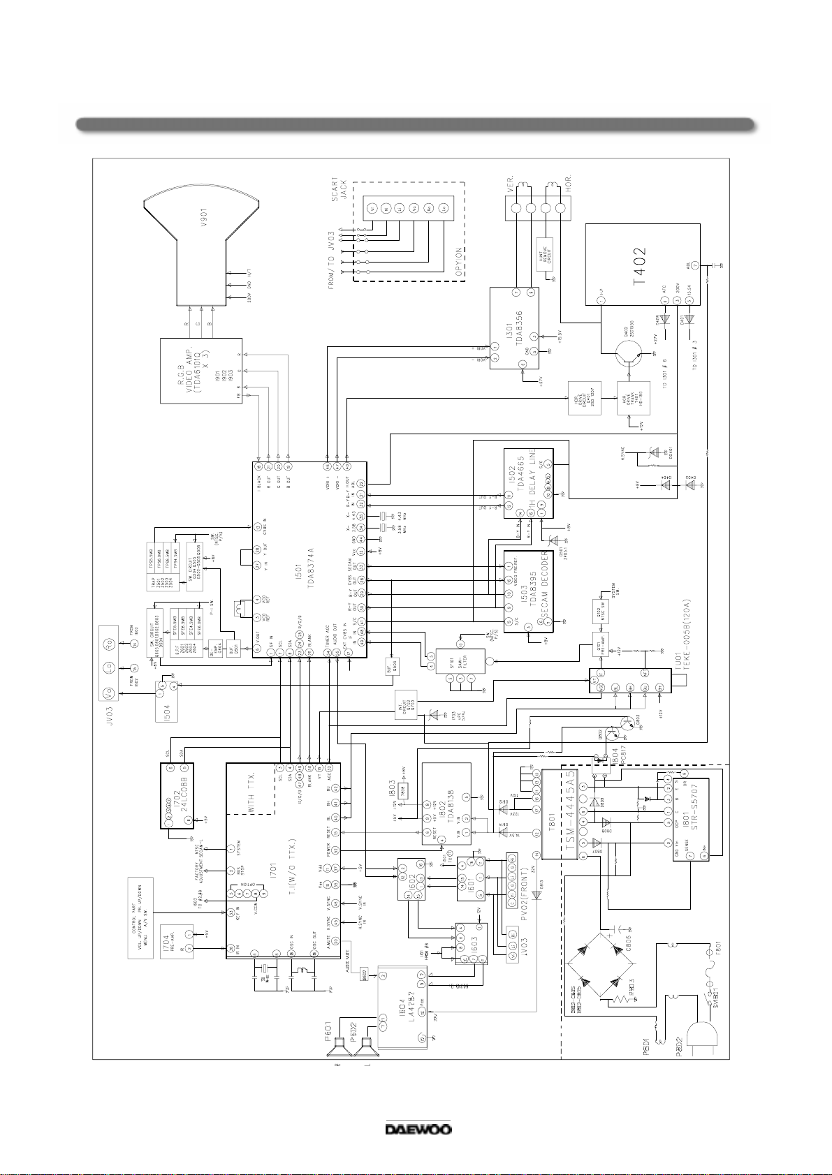
3. BLOCK DIAGRAM ................................................................................................................................ 3
4. ALIGNMENT INSTRUCTIONS ............................................................................................................. 4
5. IC DESCRIPTION ................................................................................................................................. 7
6. CIRCUIT DESCRIPTION ...................................................................................................................... 35
7. PCB LAYOUTS...................................................................................................................................... 44
7-1. PRINTED CIRCUIT BOARD
7-2. SCHEMATIC DIAGRAM
8. TROUBLE SHOOTING CHARTS ......................................................................................................... 46
9. IC DC VOLTAGE CHARTS ....................................................................................................... ........... 53
10. ELECTRICAL PARTS LIST .... .......................................................................................................... .. 56
11. CP-390 (INDIA CRT) INCH DIFFERENCE PART LIST...................................................................... 74
12. CP-390(ORION CRT)INCH DIFFERENCE PART LIST ..................................................................... 75
13. CP-390 CHASSIS CRT DIFFERNT PART LIST ................................................................................. 76
Page 3

1. SPECIFICATIONS
TV STANDARD PAL/SECAM-B/G, D/K, I, H, NTSC-3.58/4.43/5.5
MA INS V O LTAG E 100~250V AC , 50/60Hz
POWER CONSUMPTION 14T6VM=72W
20T6VM=82W
21T6VM=87W
SOUND OUTPUT 14” : 3W+3W
20” : 5W+5W
21” : 8W+8W
SPEAKER 14” : 5W 8 0hm(2EA)
20” : 5W 8 0hm (2EA)
21” : 8W 8 0hm (2EA)
ANTENNA
IMPEDANCE
TUN ING SY STE M Voltage Synthesize tuning System
ME M O RY C HA NN EL VM : 100 channels, TM : 70 channels
RECEPTION
CHANNEL UNIT
RE M OT E C O NT RO L VM : R-28B04, TM : 28B03
SCREEN SIZE
W EIGHT 14” : 9.7Kg(set)
INDICATION On-Screen Display
75 ohm unbalanced
300 ohm balanced with supplied balun
VHF - L : CH2 - CH4
VHF - H : CH5 - CH12
Cable Band : CHS1’ - CHS3’, CHS1 - CHS20
Hyper Band : CH S21 - CHS 40(option)
UHF : CH21 - CH69
14” : 34cm (A34JLL 90 02)
20” : 48cm (A48JLL 90 02)
21” : 51cm (A51JLL 90 02)
20” : 18.5Kg(set)
21” : 27.2Kg(set)
MENU
Picture(Bright, Color, C ontra st, Sharpness, TINT)
T im e r( C lo ck , Wa ke - up - T im e , A c tiv ate , Wa k e -u p -P ro g )
Language
Preset
Edit
Sleep Tim er
AV
Sound Mute
Volume Control
1
Page 4

2. SAFETY INSTRUCTION
WARNING
:
Before servicing this chassis, read the “X -RAY radiation precaution”,
“safety precaution” and “product safety notice” below.
2-1. X-RAY RADIATION PRECAUTION
1. Excessive high voltage can produce potentially hazardous X-RAY R ADIATION.To avoid such hazards,
the high voltage must not exceed the specified lim it. The nominal value of the high voltage of this receiver
is 22-23kv(14”), 25-26kv(20”, 21”) at max beam current. The high voltage must not,
under any circumstances, exceed 27.5kv (14", 20”), 29.0kv(21”).
Each tim e a receiver requires servicing, the high voltage should be checked. It is recommended the
reading of the high voltage recorded as a part of the service records. it is important to use an accurate and
reliable high voltage meter.
2. The only source of X-RAY R adiation in this TV receiver is the picture tube. For continuous RADIATION
protection, the replacement tube m ust be exactly the same type tube as specified in the parts list.
2-2. SAFETY PRECAUTION
1. Potentials of high volt age are present when this receiver is operating. Operation of the receiver outside the
cabinet or with the back cover removed involves a shock hazard from the receiver.
1) Servicing should not be attempted by anyone who is not thoroughly familiar with the precautions
necessary w hen working on highvoltage equipment.
2) Alw ays discharge the picture tube to avoid the shock hazard before rem oving the anode cap.
3) Discharge the high potential of the picture tube before handling the tube. The picture tube is highly
ev a c u a te d a n d if b ro k e n , g la s s fr a gme n ts w ill b e v io le n tly e x p e lle d .
2. If any Fuse in this TV receiver is blown, replace it with the FUSE specified in the Replacement Parts List.
3. When replacing a high wattage resistor(oxide m etal film resistor) in circuit board, keep the resistor
10mm away from circuit board.
4. Keep wires away from high voltage or high temperature com ponents.
5. This receiver must operate under AC260 volts, 50Hz/60H z.
(AC 100~250 volts, 50/60Hz)NEVER connect to DC supply or any other power or frequency.
2-3. PRODUCT SAFETY NOTICE
Many electrical and mechanical parts in this chassis have special safety-related characteristics.
These characteristics are often passed unnoticed by a visual inspection and the X -RAY RA DIATION
protection afforded by them cannot necessarily be obtained by using replacement components rated for
higher voltage, watt a ge, etc. Replac ement parts whic h hav e these specia l safet y c ha racteristics are identified
in this manual and its supplements, electrical components having such features are identified by designated
symbol on the parts list. Befor e replacing any of t hes e c omponent s , read the parts list in thi s manual c areful ly.
The use of substitute rep lacement parts which do not have the same safety characteristics as specified in t he
parts list may created X-RAY Radiation.
2
Page 5
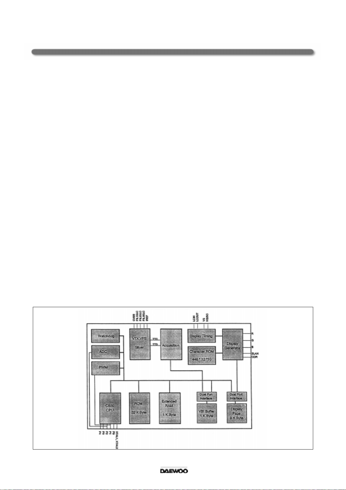
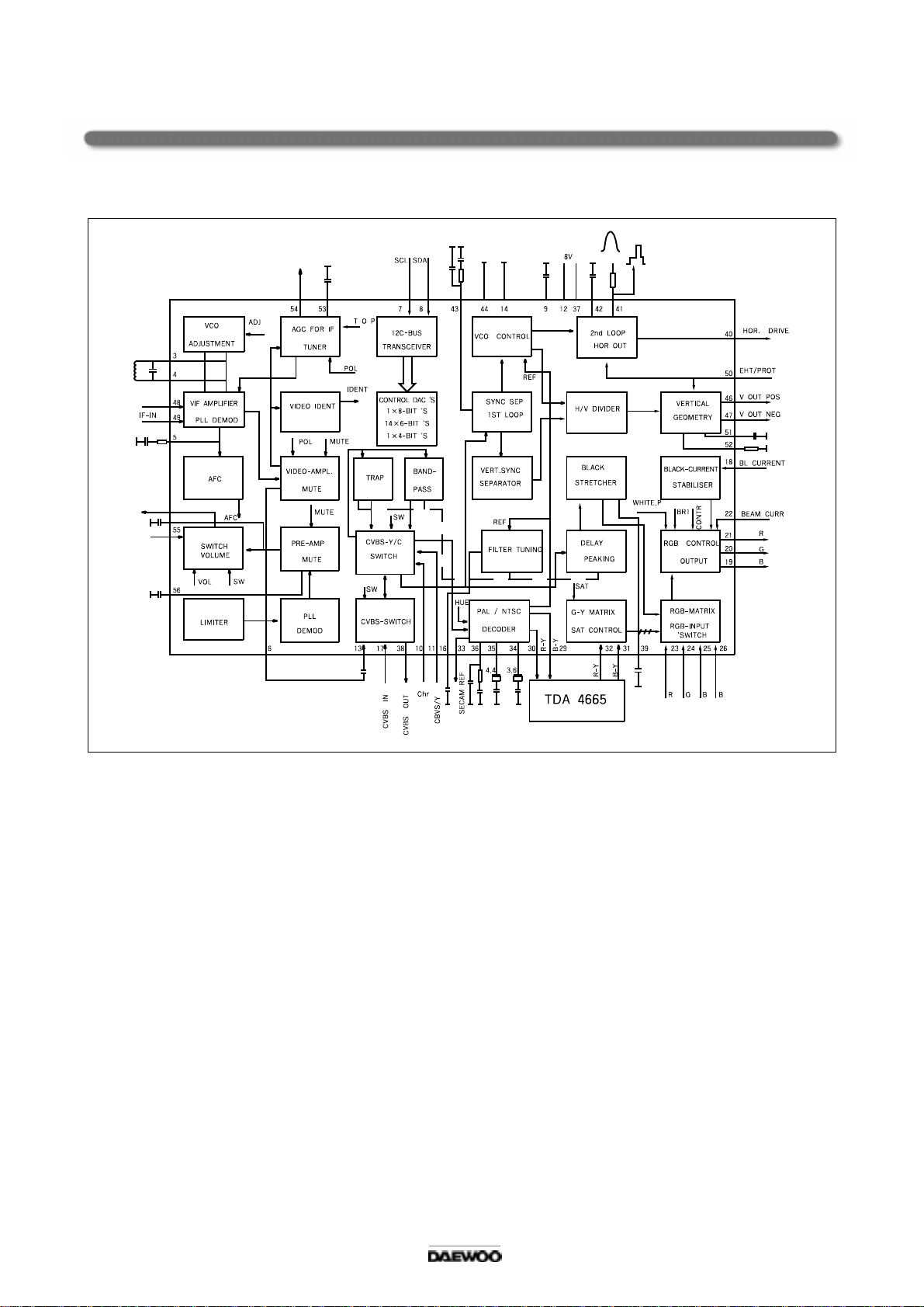
3. BLOCK DIAGRAM
3
Page 6
4. ALIGNMENT INSTRUCTIONS
4-1. AFT
1. Standard B/G, D/K, I
1) Set a S ignal Generator with
- RF FREQ UEN CY = 38.9 MHz,
- RF OUTPUT LEVEL = 80
- System = PAL / SECAM - B/G , D/K, I
NT S C - 3 .5 8 /4.4 3
2) Connect the Signal Generator RF Output to P101 (Tuner IF Output).
There must be no signal input to the tuner.
3) Press the “AFT” KEY and wait until the TV screen display “AFT OK”.
2. AGC
1) Set a Pattern Generator with RF LEVEL 632 dBuV .
2) Connect a O SCILLOSC OP E PRO BE to P101 (TUNER AGC INPUT).
3) Adjust AGC UP/DOW N KEY the voltage drop 3.5V dc point its m aximum voltage.
(TDA8374A N1 V ER SION)
Adjust AGC up/down key the voltage drop 1V dc over blow its maximum voltage
(TDA8374A n3 version)
5 dBuV
Alternative Method
1) S e t a P atte rn G e n er a tor w ith
- RF LEVEL 80
5 dBuV
- PAL CROSSHATCH
( without SOUND CARRIER )
2) Connect a O SCILLOSC OP E
( Bandwidth
100MHz ) PROBE
to P 1 0 1 (TU NER IF OU TP UT ).
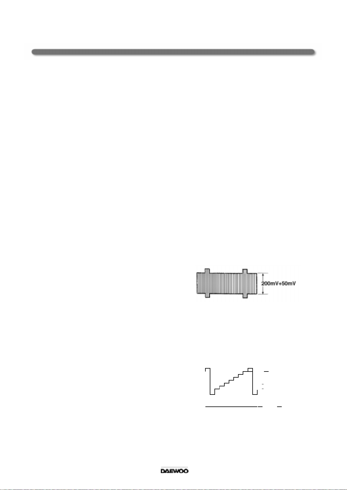
3) Use AGC UP/DO WN KEY to obtain
an envelop amplitude 200 + 50 mVp-p.
3. SCREEN
1) Apply a CO LOR BAR pattern signal.
2) Set the CONTRAST, BRIGH TNESS
to MAX , CO LOR to MIN .
3) Set the R,G,B LEVEL to CENTER (31/63)
160
5Vdc ( 20”, 21” ) with R,G,B UP/DOW N KEY.
4) Connect a O SCILLOSC OP E PRO BE
to P 9 0 4 ( CRT C A T H OD R , G , B ).
5) Adjust the SCREEN VOLUME on FBT
such that the highest black level voltage
160
5Vdc (20”, 21”), 1305Vdc (14”).
Black leve
160 + 5Vdc(20", 21")
130 + 5Vdc(14")
GND
4
Page 7
4. WHITE BALANCE
1) S e t th e TV to N OR I mod e.
2) Set the R,G,B LEVEL to CENTER with R,G ,B UP/DOW N KEY .
3) Adjust the R,G,B UP/ DOWN KEY of the ot he r c o lor which did not appear on the s cr een t o obt ai n WHITE.
5. FOCUS
1) Apply a R ETM A PATT ERN signal.
2) A d ju st th e FOCUS V OLU ME o n F B T to o b ta in o p tim a l res o lutio n.
6. GEOMETRY
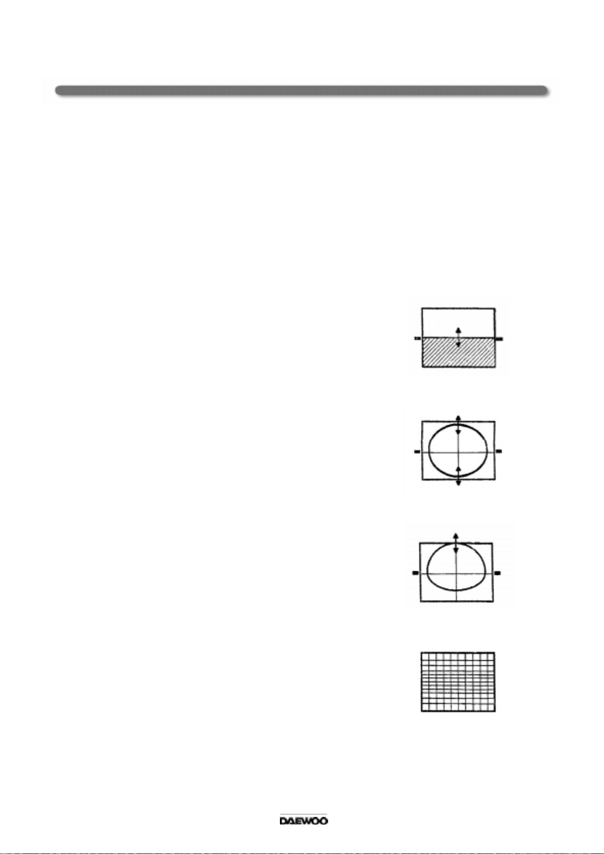
6.1 VERTICAL CENTER
1) S e t th e TV to N OR I mod e.
2) Pressing the V-SIZE UP/DOW N KEY,
the lower half of the screen is blanked.
3) Adjust the border line of blanked picture
coincident with the mechanical center marks
of the C RT using the V-CENTE R U P/DOW N KE Y.
6.2 VERTICAL SIZE
The VERT ICAL CENTE R adjustm ent
has to be done in advance.
1) Apply a R ETM A PATT ERN signal.
2) S e t th e TV to N OR I mod e.
3) Adjust the upper part of the picture
w ith th e V -S IZ E U P /D OWN k ey s.
6.3 VERTICAL SLOPE
The VERT ICAL SIZE adjustment
has to be done in advance.
1) Apply a R ETM A PATT ERN signal.
2) Adjust the lower part of the picture w ith
the V-SLOPE UP/DOWN keys.
6.4 VERTICAL S-C ORRECTION
1) Apply a CROSSHATCH PATTERN signal.
2) A d ju st th e S -C O R U P/DOW N KE Y to o bta in
the same distance between horizontal lines.
6.5 HORIZONTAL CENTER
1) Apply a R ETM A PATT ERN signal.
2) Adjust picture centering with H -CENTE R
LE F T /R IGHT k e ys .
5
Page 8
If EEPROM(1703) has been changed ;
- Option data has to be changed and
- all alignment function has to be readjusted.
The initial state of adjustment are as follows;
- V-Center, V-S lope V-Size, H-Center, R , G, B, AFT = Center (30/64 - 33/64)
- S-Correction = 00/64
- AGC = 15~60/64
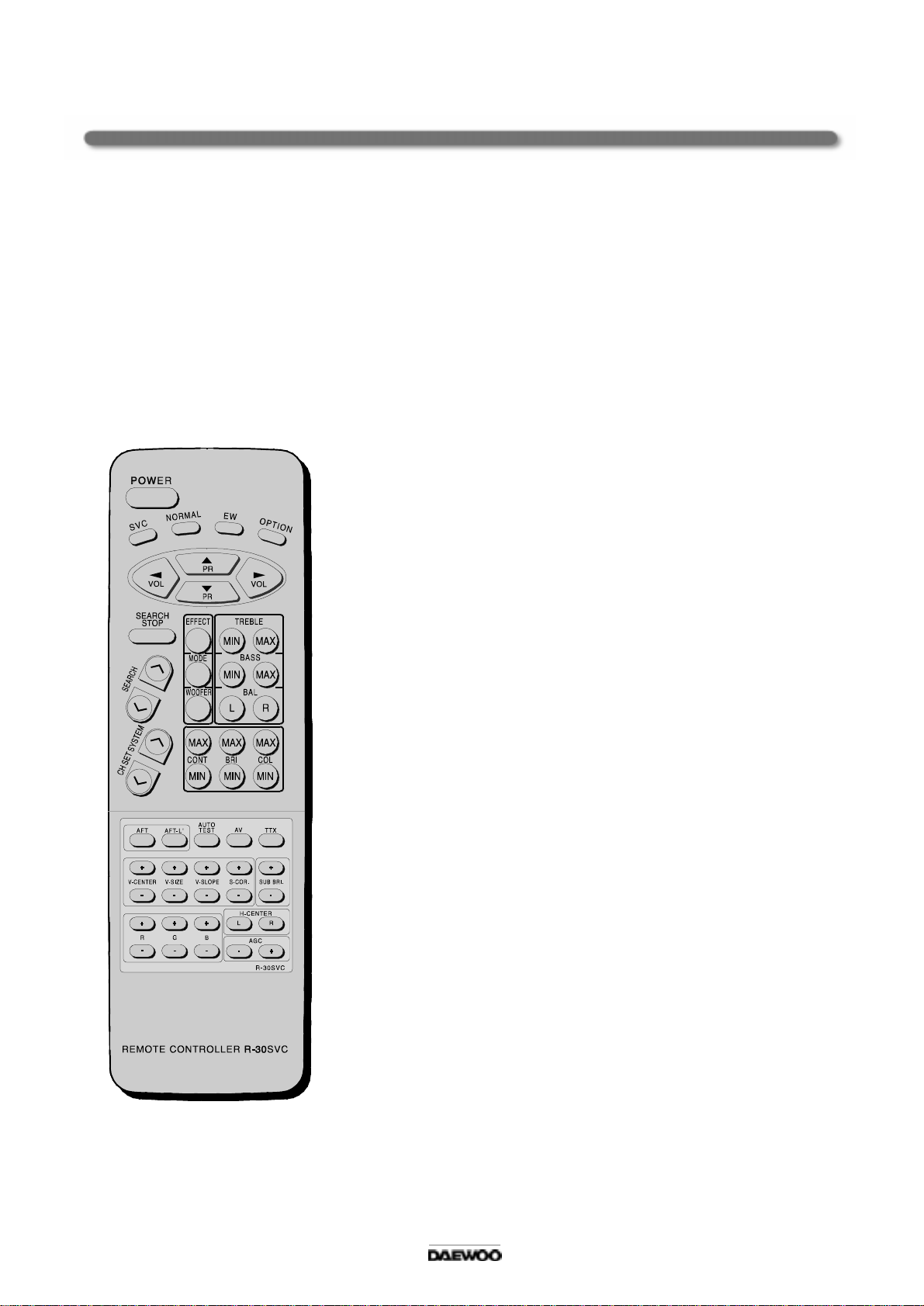
Service Remocon
6
Page 9

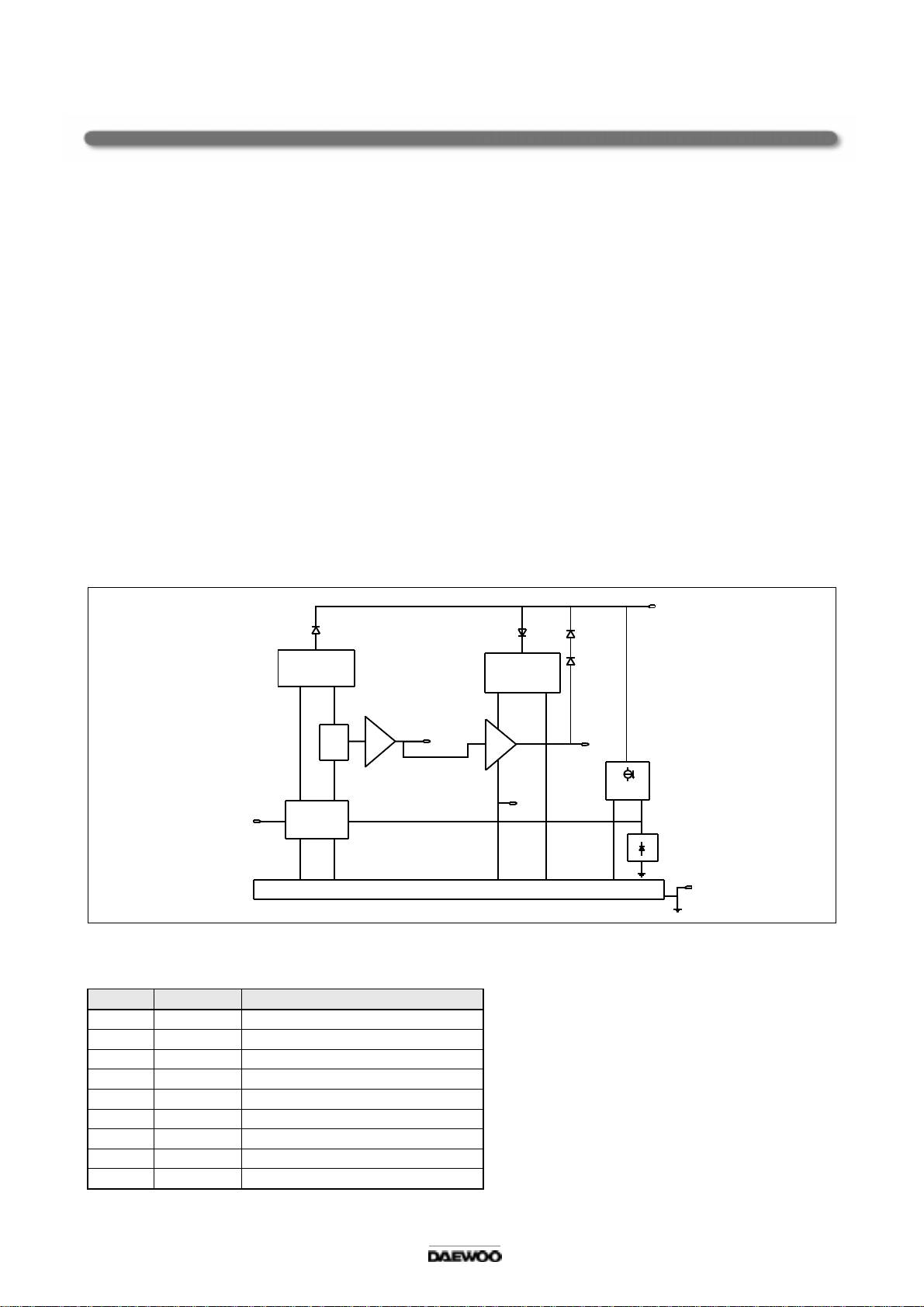
5. IC DESCRIPTION
DW370ASM* (Micro-controller for Non-Teletext Model)
=TMS370C08A05 ( TI Type No.)
1. General Description
The TMS370C 08A05 devices are mem bers of the cMCU 370 family single-chip m icrocontrollers.
The cMCU370 famil y provides cost ef fect ive real-time system control through use of the PRISM methodology.
The PRISM m ethodology m odular fabrication process integrates analog, digital, linear and power
technologies on a single chip, thereby m aximizing the total integration strategy.
The TMS370C 08A05 devices are designed with the high-performance 8-bit TM S370C8 C PU.
Features of the ‘C8 CP U and system m odule as implemented on this device include three CPU registers
(stack pointer, status register, and the program counter), two external interrupts, reset,
mem ory mapped control registers.
2. Feature
• Inte rn al Memo ry C o n figu ra tion s
- 16K-Byte ROM Program Memory
- 512-B yte RAM
• Operating Features
- Supply Voltage (VCC) 5 V
- Input Clock Frequency 2, 20MHz
- Industrial Temperature Range
• Device Integrity Features
- Address Out-of-Range Reset
- Stack Overflow R eset
- Parallel Signature Analysis (C RC)
• Two 16-Bit G eneral P urpose Tim er(T8A)
Each Includes:
- 16-Bit R esettable Counters with individual 8-B it Prescaler
- 2 PWM Channels or
- 2 Input Captures or
- 1 Input Capture and 1 PWM Channel
• One 14-Bit PWM M odule
- 14-Bit R esettable Counters
- 14-B it PWM O utpu t Po rt
• One 8-Bit PWM M odule
- 8-Bit R esettable Counters
- 8-Bit PW M O utput P ort with 12V O pen Drain
• O S D Mo d u le
- Blanking/ Contrast reduction out
- Transparent Background
- Transparent Foreground
- Full Screen Background Color
10%
7
Page 10
- Controlled Color, Blink, Size, Smoothing, Fringe of Each lines of C haracter
- Two size of different Font 12
- OSD W indow Display with 40
10 and 1218 by Hard Masking
25 lines
• 8-B it A /D Converter With 3 Inputs
- Single or Dual C hannel Operation
- Single or Continuous Conversion Modes
• Fle x ible Inte rru p t H a nd ling
- Global and Individual Interrupt Masking
- 2 S/W P rogramm able Interrupt Levels
- 2 External Interrupt (1 Non-Maskable)
- Programmable Rising or Falling Edge Detect
• 09 CMOS Compatible I/O Pins
- All Peripheral Function Pins Software Configurable for Digital I/O
- 6 Bidirectionals, 3 Input Pins
• Plastic 42 YSDP Pins Package
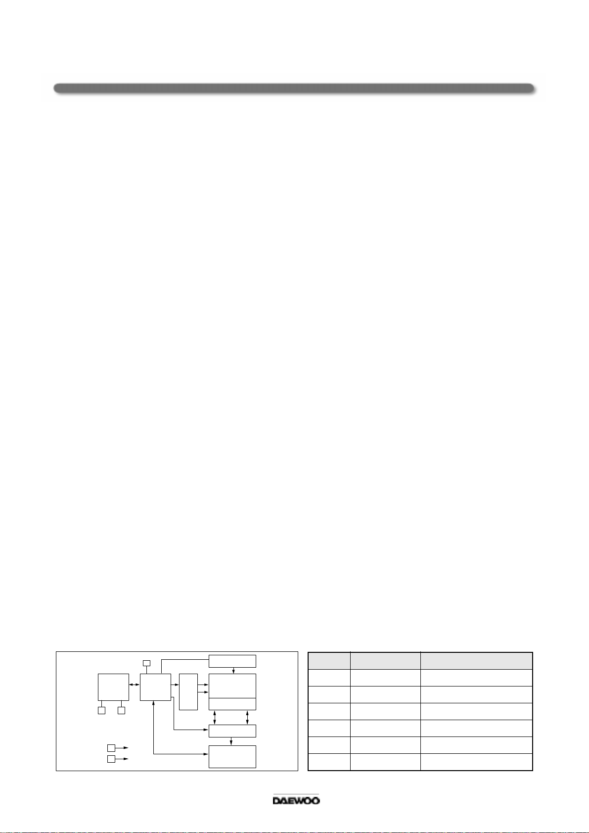
3. Block Diagram
INT1/VPP INT2 OSCIN OSCOUT TEST RESET O SCOUT_OSD OSCIN _OSD V-SYNC H-SYNC VCC_OSD
Interrupt
RAM
512-byte
EPROM/ROM
Program Memo ry
16K-byte
Port A
Port B
Multipiexed
With AN0-AN3
63
1/2 Clock
Oscillator
System
Control
TMS3 70C8
CPU (C8)
A-to-D Converter
3
VCC VSSB0/AN0-B2/AN2AO-A5
(ADC)
OSD
8 bit PWM
14 bit PW M
Tim e r 1 (T 8A 1 )
Timer 2 (T8A2)
6
2
COR
BLANK
RED OUT
GREEN OUT
BLUE OUT
VSS_OSD
PWM1_0/5
PWM2_0/1
T8A1IC1/CR
T8A1IC2/PWM1
T8A1IEVT/PWM
T8A2IC1/CR
T8A2IC2/PWM1
T8A2EVT/PWM
8
Page 11

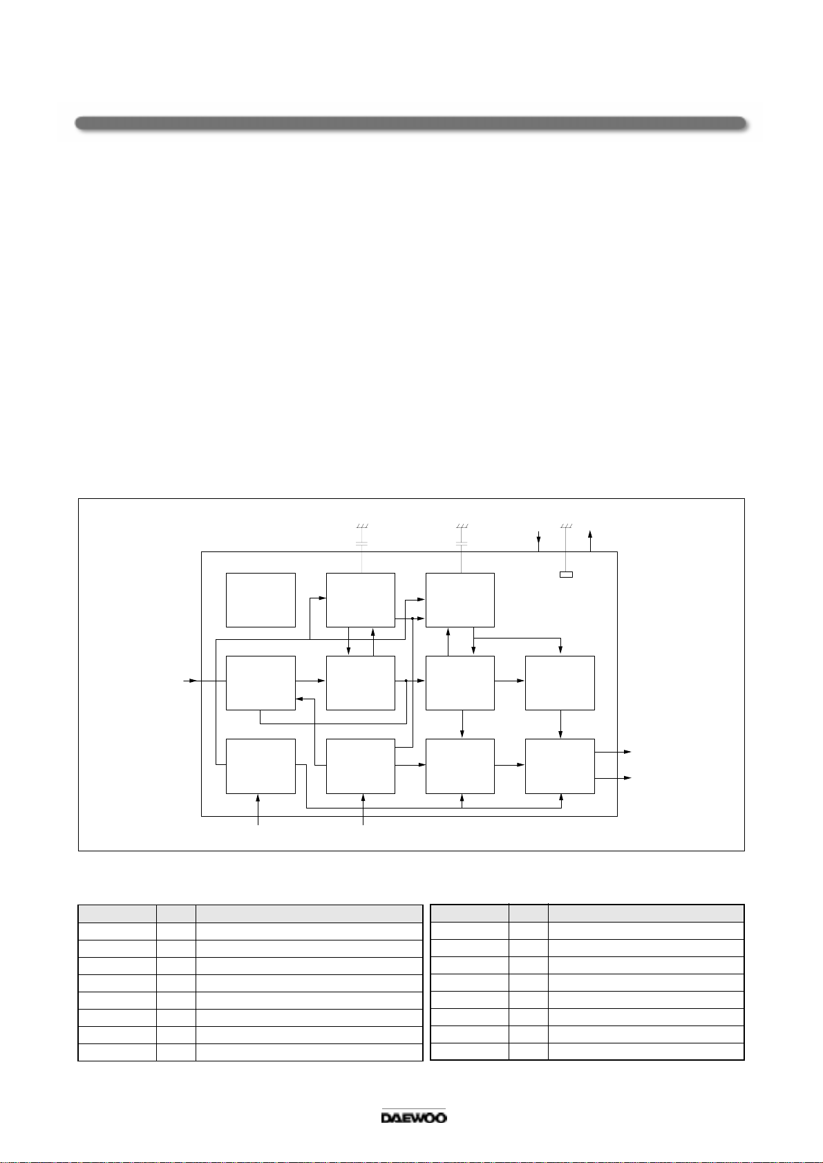
DW5255M*(Micro-controller & West/East Teletext Decoder)
DW5255RM*(Micro-controller & Cyrillic Teletext Decoder)
=SDA5255-A*** (SIEMENS Type No.)
1. General Description
The TDA5255 contains a slicer for VPS and TTX, an accelerating acquisition hardware module, a display
generator for “LEVEL 1” TTX data and a 8 bit u-controller running at 333 nsec cycle time.
The controller with dedicated hardware guarantees flexibility, does most of the internal processing of TTX
acquisition , t ransfers data to/from the external memory interface and receives/transmits data via I2C and
U A R T u se r inte rfa ce s .
The Slicer combined with dedicated hardware stores TTX data in a VBI 1Kbyte buffer.
The u-controller firm w are does the total acquisition task (ham m ing- and parity -checks,
page search and evaluation of header control bits) once per field.
2. Feature
• A cq u isition :
- feature selection via special function register
- sim ultaneous reception of TTX and VPS
- fixed framing code for VPS and TTX
- programm able framing code window for TTX
- Acquisition during VB I
- dire c t ac ce s s to V B I R A M bu ffe r
- Acquisition of packets x/26, x/27, 8/30 (firm w are)
- assistance of all relevant checks (firmware)
- 1-bit framing-code error tolerance (switchable)
• Display:
- features selectable via special function register
- 50/60 H z display
- level 1 serial attribute display pages
- blanking and contrast reduction output
- 8 direct addressable display pages
- 12 x 10 character m atrix
- 96 character ROM (standard G0 character set)
- 143 national option characters for 11 languages
- 288 characters for X/26 display
- 64 block mosaic graphic characters
- 32 free addressable characters for OSD in expanded character ROM + 32 inside OSD box
- double height (TOP/BOTTOM )
- conceal/reveal
- transparent foreground/background -inside/outside of a box
- cursor (colour changes from foreground to background colour)
- flash (flash ra te 1 s)
- programm able horizontal und vertical sync delay
9
Page 12
- hardware assisted fast display page erase
- full screen background colour in outer screen
• Synchronization:
display synchronization to sandcastle or Horizontal Sync (HS) and Vertical Sync (VS) with
star ts to p -o s c illa to r or d ispla y s y n c h ro n iz a tio n to s andcastle or Horizontal Sync and Vertical Sync with
external clock independent clock systems for acquisition, displa y and con troller
• C on tro ller:
- 8 bit co nfiguration
- 20 MHz internal clock
- 0.33 us instruction cycle
- eight 16-bit data pointer registers (DPT R)
- tw o 16 -b it tim ers
- watchdog timer
- serial interface (UART)
- 256 bytes on-chip R AM
- 1 Kbyte on-chip extended RAM (access via M O VX)
- 8 Kbyte on-chip ACQ -buffer-RAM (access via MO V X)
- 6 channel 8-bit pulse width m odulation unit
- 2 channel 14-bit pulse width m odulation unit
- 4 multiplexed AD C inputs with 8-bit resolution
- one 8-bit I/O port with open drain output and optional I2C em ulation
- tw o 8-bit multifunctional I/O ports
- one 4-bit port w orking as digital or analog inputs
- one 2-bit I/O port with optional address latch enable function
• P -S D IP 5 2 p a c ka ge
• 5 V supply voltage
3. Block Diagram
10
Page 13
4. Pin Descriptio n
(A* : D W5255M */DW5255RM *, B* : DW370AS M *)
Pin Name Symbol Descriptio n
A* B* A* B* A* B*
1
1 P 3 .1 T1 IC1/ C R S Y S N TSC O UT for switc h in g SA W filte r
2 2 P0.7/Open Drain A0 BU SS TO P I2C BUS STO P IN for Com puter
3 3 P0.6/Open Drain A1 SDA Serial data IN/OUT for I2C
4 4 P0.5/Open Drain A2 SCL Serial clock IN/OU T for I2C
K6259
- PAL/SECAM : L
- N TS C : H
controlled alignm ent in Factory
( A c tiv e L o w )
5 5 P0.4/Open Drain A3 O PTION #5 #6 Teletext
6 6 P0.3/Open Drain A4 O PTION
7 7 P0.2/Open Drain A5 OPTION Not Used
8 8 P0.1/Open Drain PWM 1-0/ Open D rain OP TION Not Used
9 9 P0.0/Open Drain PWM 1-1/ Open D rain LED LED drive OUT
10 10 VSS VSS ground
11 11 VC C VCC Power Supply
12 12 XTA L1 OS CIN OS CIN Input to inverting osc. Amplifier
13 13 XTA L2 OS CO U T OS CO U T Output of inverting osc. Amplifier
14 14 P4.0/ALE PW M 1-2/Open D rain N ot Used H : I/M, L : B/D
15 15 RE SET RES E T/Open D rain RST RE SET IN (ACTIVE LOW)
16 16 P1.7/14BIT PW M PW M 2-0 VT TUN ING V OLT AG E O UT
17 17 P 1.6 /14 B IT PWM P WM 2 -1 S W H : I/M
H H Wes t T e le tex t
L H E a s t Te le te x t
H L T urkish Teletext
- Stand-by mode : H
- Operating mode : L
( IR reception : pulse )
L : B/D
#6
H : STAND-BY
L : POW E R ON
Not Used
18 18 P1.5/8BIT PWM PW M 1-3/Open D rain F/SW Not Used
19 19 P1.4/8BIT PWM PW M 1-4/Open D rain N ot Used
20 20 P1.3/8BIT PWM PW M 1-5/Open D rain MU TE AU DIO M U TE O UT
21 21 P1.2/8BIT PWM TES T GN D (Must be tied 0V for DW 370M *)
22 P1.1/8BIT PW M Not Used
11
Page 14

Pin Name Symbol Descriptio n
A* B* A* B* A* B*
23 P1.0/8BIT PW M Not Used
24 VSSA VSSA Analog GND for Slicer
25 FIL3 FIL3 PLL Loop Filter I/O for Phase Shifting
26 FIL2 FIL2
27 FIL1
FIL1
PLL Loop Filter I/O for TTX S licing
PLL Loop Filter I/O for VPS Slicing
28 VC C A VCC A Ana log Supply for Slice r
29 IREF IREF Reference Curren t for Slicer PLLs
30 CVBS CVBS CVBS IN
31 P2.3/8 bit AD C Not Used
32 22 P2.2/8 bit ADC B0/AN0/ADC AGC IF AGC INPUT for Auto Tuning System
33 23 P2.1/8 bit AD C B 1/AN1/ADC KS Local KEY SC AN IN
34 24 P2.0/8 bit AD C B 2/AN2/ADC S/SW Not Used
35 25 VSS VSS-OSD VSS Ground
36 2 6 P 3 .3 /INT1 IN T 1 IR R EMO T E IR IN
37 27 VD D VCC -OS D VD D Power Supply
38 28 LCIN OS CIN-OSD LCIN CLO CK IN for OSD
39 29 LCOUT OSCOUT-OSD LCOUT CLOCK OUT for OSD
40 30 P3.7/TXT I/O T2EVT/PWM 2 BL BAND VHF-L OUT ( Active High )
41 31 P3.6/RXD T2 IC2/PWM 1 BH BAND VH F-H O UT ( Active High )
42 32 P3.5/T1 T2IC1/CR BU BAND UHF OUT ( Active High )
43 33 P3.4/T0 T1EVT/PW M2 POWER POWER CONTROL OUT
44 34 P3.2/IN T0 INT2 Not Used
45 35 HS/SC HSYNC HSYNC HOR. SYNC. IN(Active High)
46 36 P4.7/VS VSY NC VSY NC VER T. SYN C. IN(Active H igh)
47 37 R R RE D O U T
48 38 G G GR EEN O UT
49 39 B B BLUE OU T
50 40 BLAN K BL B LAN K O UT
51 41 COR COR Not Used
(CONTRAST REDUCTION OUT)
52 42 P3.0 T1C2/PW M 1 EVEN/
ODD
12
EVE N/OD D O UT for non-interlacing
in T TX m o de
Page 15
I702 24LC08B (EEPROM)
1. Features
• Single supply w ith operation down to 2.5V
• Low power CMOS technology
- 1mA active current typical
- 10
A standby current typical at 5.5V
- 5
A standby current typical at 3.0V
• Organized as two or four blo cks of 256 bytes (2
• Two wire serial interface bus, I
• Schmitt trigger, filtered inputs for noise suppression
• Output slope control to elim inate ground bounce
• 100KHz(2.5V) and 400KHz(5V) compatibility
• Self-timed w rite cycle(including auto-erase)
• P ag e -w rite bu ffe r fo r up to 1 6 b y tes
• 2ms typical write cycle time for page-w rite
• H ar dw a re w rite pr ote ct fo r e n tire mem o ry
• Can be operated as a serial ROM
• Factory programming(QTP) available
• ESD protection > 4,000V
• 1,000,000 ERASE /WRITE cycles(typical)
• D ata re te ntio n > 4 0 ye a rs
• 8-pin DIP, 8-lead or 14-lead SO IC packages
• Available for extended temperature ranges
- Comm ercial : 0°C to + 70°C
- Industrial : -40°C to + 85°C
2 CTM
co mpat ib le
2568) and (42568)
2. General Description
The Microchip Technology Inc. 24LC08B is a 8K-bit Electrically Erasable PROM .
The device is organized as four blocks of 256x9bit mem ory w ith a two w ire serial interface. Low vo ltage
design permits operation down to 2.5 volts w ith standby and active currents of only
5
A and 1mA respectively.
The 24LC08B also has a page-write capability for up to 16 bytes of data.
The 24L08B is available in the standard 8-pin DIP surface m ount 80IC packages.
3. Block Diagram 4. Pin Description
I/O
CONTROL
LOGIC
SDA SCL
CC
V
SS
V
WP
MEMORY
CONTROL
LOGIC
XDEC
HV GENERATOR
EEPROM ARRAY
(4X256X8)
PAGE LATCHES
YDEC
SENSE AMP
R/W CONTROL
PIN SYMBOL DESCRIPTION
1-3 A0, A1, A2 Device Address lnputs
4 V ss Ground
5 SD A Serial Da ta/A dd res s
6 S CL Serial Clock
7WP
8 Vcc +5V Power supply
13
Page 16

I501 TDA8374A (Single chip TV Processor for Negative modulation IF )
TDA8374 (Single chip TV Processor for Negative & positive modulation IF)
1.
General Description
The TDA8374(A) is I2C-bus controlled single chip TV processors which are intended to be applied in
PAL/N TSC television receiver.
The IC is m ounted in a S-DIL 56 envelope.
2. Feature
• IF
- Vision IF amplifier with high sensitivity and good figures for differential phase and gain
- PLL demodulator with high linearity offering the possibility fo r (s in g le s tandard) intercarrier stereo
audio application .
- Alignment PLL via I2C
- [T DA8374] Multistandard IF w ith negative and positive modulation, switchable via I2C
• A U D IO
- Alignment free multi standard PLL audio demodulator (4.5 to 6.5 M Hz.)
- Mono volume control
• V ide o
- Integrated luminance delay line
- Integrated chroma trap and bandpass filters (auto calibrated)
- Asymmetrical peaking circuit in the lum inance channel
- Black stretching of non standard CVBS or luminance signals
• C olo u r
- SECAM interface for application with SECA M add-on TDA8395.
• R G B
- R G B c on tro l (brig h tn es s, c o ntra s t, sa tu ratio n )
- Black current stabilization and white point adjustment
• Inp u t / O u tpu t
- Flexible video source select with CVBS input for the internal signal and two external video inputs
(one switchable for CVBS or Y/C).
- The output signal of the video source select is externally available
(also as CVBS when Y/C input is used).
- External audio input.
- Linear RGB input with fast blanking.
• Synchronization and Deflection
- Horizontal synchronization with two control loops and alignment free horizontal oscillator.
- Slow start and slow stop of the horizontal drive output to enable low stress start-up and
switch-off from the line circuit at nominal line supply voltage.
- Vertical count-down circuit for stable behavior with provisions for non-standard signals.
- Vertical geom etry control.
- Vertical drive optimized for DC coupled vertical output stages.
14
Page 17
• C on tro l
- F ull I2 C b us co n tro l, as w e ll for c us to m e r c on tro ls a s for fa c tory a lign m e n t.
- All automatic controls have an option for forced m ode.
• Power consumption
- Low power consumption (900 mW at 8.0 Volts).
• Packaging
- SDIL-56 (Shrinked Dual In Line, 56 pins).
3. Pinning Diagram of Sdil-56
SOUND IF INPUT
EXT AUDIO INPUT
VCO R EF FILTER
VCO R EF FILTER
PLL LOO PF ILTER
IF VIDEO OU TP UT
BUSINPUT : SCL
BUSINPUT : SDA
BANDGAP DECOUPLING
CHROMA INPUT
Y/CYBS INPUT
MAIN POSITIVE SUPPLY
INT C Y B S IN P U T
GROUND
AUDIO OUT
DECOUPLING FILTER TUNNING
EXT CVBS INPUT
BLACK CURRENT INP
BLUE OUTPUT
GREEN OUTPUT
RED OUTPUT
Y-GUARD INP/BEAM CUR LIMITER
RED INPUT
GREEN INPUT
BLUE INPUT
RG B INSE R T IO N S WIT C H IN P
LUM INANC E INP UT
LUMINANCE OUTPUT
1
2
3
4
5
6
7
8
9
10
11
12
13
14
15
16
17
18
19
20
21
22
23
24
25
26
27
28
SDIL56
56
DECOUPLING SOUND DEMODULATOR
55
AUDIO DEEMPHASSIS
54
TUNER AGC OUTPUT
53
AGC DECOUPLING CAPACITOR
52
REREFERENCE CURRENT INPUT
51
VERT. SAWTOOTH CAPACITOR
50
EHT/OVERVOLTAGE PROTECTION INP
49
IF IN PU T
48
IF IN PU T
47
VERT. DRIVE NEG
46
VERT. DRIVE POS
45
EAST-WAST DRIVE
44
GROUND
43
PHI1 FILTER
42
PHI2 FILTER/FLASH PROT
41
SANDCASTLE OUTP/FLYBACK INP
40
HOR. OUTPUT
39
BLACK PEAK HOLD CAPACITO R
38
CVBS OUTPUT
37
POSITIVE SUPPLY
36
LOOPFILTER BURST PHASE DET
35
X-TAL (4.43/3.58)
34
X-TAL (3.58)
33
SECAM REF OUTPUT
32
(R-Y ) INP U T
31
(R-Y ) INP U T
30
(R-Y ) OUT PUT
29
(B-Y) OUT P U T
FIG 1 : Pinning diagram of SDIL-56
15
Page 18
4. Block Diagram
16
Page 19

5. Pin Descriptio n
No Name Description
1 SOUND IF INPUT The sound equivalent in put impedance is 8k5 ohm // 5pF wh ich has to be
tak e n into a c c o u n t fo r p rop e r te r min a t ion o f th e c e ra mic filte rs .
The DC impedan ce is very high.
The m inimum input signal for catching is l mV rms.
2 E XT A U DIO INPU T A n external sound signal (5 00m Vrm s) for example from S CA R T can be
applied to this pin via a coupling capacitor.
The input im peda nce is 25kohm.
3
VCO R EF F ILTER The IF VC O tuned circuit is applied to these pin.
4
5 P LL LOO P FILTER The PLL loopfilter is a first order filter with R=390 ohm and C = 100nF in
6 IF VIDEO O U TPU T A lthough the video output impedance is low it is recommen ded to avoid
7 B US I NPUT : SCL S e r ia l clo c k line
8 B US I NPUT : SDA Se r ia l da ta line
9 BANDGAP
DECOUPLING
10 CHROMA INPUT The supplied C S -VHS input burst amplitude should be nominally 300mV pp
11 Y/CVB S INPU T The Y S -VHS signal of 1V pp ( inclusive sync amp litude) is AC coupled to pin1 1.
12
37
MAIN
POSITIVE SUPPLY
Its resonance frequency must be two tim es the IF-frequency and in between a
range of 64-120MHz.
This range is suitable for the IF standards as 33.4, 38 .9, 45.75 and 58.75MH z.
The VC O frequency can be adjusted b y I2C bus so a fixed coil can be used.
serie s to ground.
The loopfilter bandwidth is 60kHz and is optimal for both fast catching and
sufficient video suppression for optimal sound perfo rmance.
Sound performance can theoretically be improved by adding a small
capacitor (approx.0- 4.7nF) betw een pin 5 and ground.
This however must be evaluated further because the normal video signal
response should not be effected.
high frequency current in the output due to for instance sound trap filters.
This can be achieved by m eans of an emitter follower at the video o utput with
a 1
resistor in series with the base
The bandgap circuit provides a very stable and temperature independent
reference voltage.
This reference voltage (6.7V) ensures optimal performance of the TDA8 374
and is used in almost all functional circuit blocks.
(assumed is a colour bar signal with 75% saturation and with chroma/burst
ratio of 2.2/1 ). The C S-VHS input is internally clamped to 4V via 50
The external AC coupling capacitor with 50
A recomm ended coupling capacitor is 1 nF; the high pass filter cut off
frequency is the n approximately 3K H z.
The TD A8374 ha s a m ain supply pin 12 and a horizontal supply pin 37. Both
pins have to be supplie d simultaneously.
Notice that the IC has not been designed to use this pin 37 as start pin.
(pin 37 supplies the horizonta l oscillator, PHI-1 and PHl-2)
(pin 12 supplies the rest of the circuits in the IC)
The nom inal supply voltage is 8V. With min/max values of 7.2-8.8V.
Also in stand-by condition the IC must be supplied with 8V.
A voltage detection circuit is connected to both pins.
- pin12 if V 12 <6.8V than a power on rese t, POR , is generated.
The Hout output is disabled immediate.
- pin37 if V37 <5.8V than the horizon tal output is disabled imm ediate.
.
forms a high pass filter.
.
17
Page 20

No Name Description
13
17
14 G RO UN D All inte rnal circuits are connected to this ground pin 14.
15 AU D IO O UTP U T T he output signa l is volume controlled and is active fo r both internal and
16 DECOUPLING
18 BLACK CURRENT
19
20
21
22 V-GUARD INPUT/
INT CVBS INPUT
EXT CVBS INPUT
FILTER TUNING
INPUT
BLUE OUTPUT
GREEN OUTPUT
RED OUTPUT
BEAM CURRENT
LIMITER
It is recomm ended that the CVBS1 int and CVBS2 ext input am plitudes are
1 Vpp (inclusive sync amplitude).
This, because the noise detector switches the
(i.e . a u to
100mV rms (i.e. at S/N of 20dB).
external audio signals. The nominal gain is +9dB and -71dB, which gives
a total control range of 80dB.
The output signa l range therefor is 0.14- 1400mVrms
The bandw idth is >100kHz, the DC level is 3.3V and the output im pedance
is 2 5 0
Voltage variations at pin 16, which can be due to external leakage current or
crosstalk from interference sources, should be less than 50mV to ensure that
tuning of filters/delay cells remains correct.
For correct operation of the loop CURRENT inform ation is supplied to the
black current input pin.
The RG B outputs are supplied to the video output sta ges from pins 21, 20
and 19 respectively.
For nominal signals (i.e. C VBS/S-VHS, -(R-Y)/- (R-Y), TXT inputs) and for
nominal control settings, then the RGB output Signal amplitu des is
typically 2VBLACK_WHITE.
1mode w hen FOA , FOB = 0,0) when noise level exceeds
.
1 loop to slow mode
Vertical Guard
With this function, the correct working o f the vertical deflection can be
monitored. If the vertical deflection fails, the RGB outputs are blanked to
prevent damage to the picture tube.
Be a m cu rre nt limitin q
The beam current limiting function is realise d by reducing the contrast (and
finally the brightness) when the beam current reaches s too high level. The
circ u it fa lls a p a rt in tw o fun c tio n s :
- Average beam current limitin g (ABL): re acting on the average content of
the picture
- Peak white limiting (PWL): reacting on high local peaks in the RGB signal.
23
24
25
26 RGB INSERTION
27 LU M INAN CE INPU T An nom inal input signal am plitude of 1 Vblack-white MU ST b e DC coupled
RED INPUT
GREEN INPUT
BLUE INPUT
SWIT C H INPUT
The Rin, Gin, Bin input signals (nominal signal amplitude of 700mV ) are
AC coupled to pin 23, 2 4 and 25 respectively.
Clamping action occurs durin g burstkey period.
The table below a survey is given of the three modes which can be selected
with a voltage on R G B insertion switch input pin ;
V p in 2 6 I2 C fu n ctio n Se le c te d RGB s ig n a l
0.9 V - 3V IE 1 = 0 R GB(in te rn a l)
IE1 = 1 Rin ,Gin,B in
(fast insertion on pin23,24,25)
> 4 V IE 1 =X O SD c a n b e in s e rted a t the RGBo u t p in s
to the luminance input pin 27.
The pin is internally AC coupled to the luminance clamp via a capacitor of
50pF; clamping action occurs during burstkey period.
18
Page 21

No Name Description
28 LUMINANCE
OUTPUT
29
30
31
32
33 SECAM REF
34
35
36 LO OP FILTER
38 CVBS OU TPUT The output amplitude is 1Vp-p (transfer gain ratio between CVBS1int or
39 BLACK PEAK
40 H OR O U TPU T T his open collector output is mean t to drive the horizontal output stage.
41 SANDCASTLE
42 PH I-2 FILTER /
B-Y OUTPUT
R-Y OUTPUT
B-Y INPUT
R-Y IN PUT
OUTPUT
X-TAL 3.58
X-TAL 4.43
BURST PHASE
DETECTOR
HOLD CAPACITOR
OUTPUT/
FLYBACK INPUT
FLASH PROTECT
The luminance output signal is approximately l V black-white with typical
output im pedance of 25O ohm .
The ma ximum output im pedan ce of pins 29 and 30 is 500
signals are identified. W hen S EC AM is identified by the SECAM add-on and
no PAL/NT SC is alread y identified by the ASM , then the ASM sets the
-(B-Y)/-(R-Y) output switch open (via DEMSW).
This enables the -(B-Y)/-(R-Y) outputs of the TDA 8395 to be directly connected
to pins 29 and 3O respectively.
The -(B-Y),-(R-Y) output signals (supplied from ba seband delay line) are AC
coupled, via a coupling capacitor of 10nF or greater, to the -(B-Y)/-(R-Y) inputs;
both inputs are clam ped during burstkey period.
The SE CA M reference outpu t is directly connected to pin 1 of the TDA 8395 for
SEC AM decoding ; it also can be used as a reference for comb filter applications.
To ensure correct operation of both:
- colour processing in ternal circuits,
- sync calibration internal circuits,
it is only allowed to have 3.6MHz Xtals on pin34: both 4.4MHz,3.6MHz X tals
are allow ed on pin 35.
If pin 35 is not used: then it is left open in application (also XA,XB=O,1 ).
One of the important aspects of the PLL is the loop filter connected to pin 36;
it influences the dynamic performance of the loop .
CVBS2ext or CVBS3ext/Ys-vhs and CVBSout is 1).
The m aximum output impedan ce is 250 ohm.
For the correct working of the black stretcher an external tim e constant should
be added at the black peak hold capacitor input.
The output is a ctive low, i.e. the line transistor should conduct during the low
period of the output.
Pin 41 is a combined in put/output pin.
The pin provides a three level sandcastle pulse.
Both burstkey pulse and vertical blanking pulse are alw ays available, the line
blanking pulse is only present when the external flyback pulse is fed to this pin.
The line flyback pulse, fed to this pin is used for tw o functions:
- input signal for the PHI-2 1oop and
- RGB line blanking . (without flyback pulse blankin g occurs only during the
burstkey pulse)
To ensure correct working of the delay line and SECAM add-on, the output
should not be loaded with more than:
- Sandcastle input delay line TDA 4665
- Sandcastle input SECA M add-on TD A 8395
The loopfilter is a first order filter.
This pin requires a capacitor (C) only.
A flash protection becomes active when this pin is forced > 6V. The horizontal
drive is switched-off immediately.
Once the voltage is <6V the horizontal drive is switched-on again via the slow
start procedure.
when PAL/NT SC
19
Page 22

No Name Description
43 PH I-1 FILTER T he loopfilter connected to pin 43 is suitable for various signal conditions as
strong/weak and VCR signal.
This is achieved by switching of the loopfilter time constant by changing the
PHI-1 output current.
Via I2C bus FOA/B, different tim e constants can be chosen, inclu ding an
automatic mode w hich gives optimal performance u nder varyin g conditions.
44 G RO U ND T o this pin are connected the IC-substrate and horizontal output.
45 EAST-WEST DRIVE not used
46
47
48
49
50 EHT/OVERVOLTAGE
51 VERT
52 REFERENCE
53 AG C
54 TUNER AGC
55 AUDIO
56 DECOUPLING
VERT DRIVE +
VERT DRIVE -
IF INPU T The PLL frequency range is 32-60MHz with corresponding VCO frequency
PROTECT INPUT
SAWTOO TH
CURRENT INPUT
CAPACITOR
OUTPUT
DEEMPHASSIS
SOUND
DEMODULATOR
The vertical drive has a current output. The output is bala nced which ensures
a good com m on m ode beh avior with temperature and makes the output signal
less sensitive for disturbances.
64-120MHz.
The IF input impedances is 2
load for comm only used SAW filters.
A DC coupling is allowed, so no series capacitors between SAW filter and IF
input are necessary.
not used
This pin requires a capacitor to ground of l00nF +, - 5%.
The optimal sawtooth amplitude is 3.5V and is determined by the external
The sawtooth bottom -level is 2V.
This pin requires a resistor to ground.
The optimal reference current is 100
The AG C capacitor value is 2.2
comprom ise between AGC speed and tilt for all AGC m odes
(negative/positive modulation).
This output is used to control (reduce) the tune r gain for strong RF signals.
The tuner AGC is an open collector output which is acting as a variable
current source to ground.
Only a capacitor has to be connected to this pin that defines the deemphasis
tim e constant.
The signal is internally connected through to the A udio switch.
The deem phasis output is fixed, thus not controlled by the volume, and can be
used for SCART.
This pin requires a capacitor of 10
The pin acts as a low pass filter needed for the DC feedback loop.
in parallel with 3pF and matches the required
. which is determined by this resistor.
and has been defined for an optimal
connected to ground.
20
Page 23
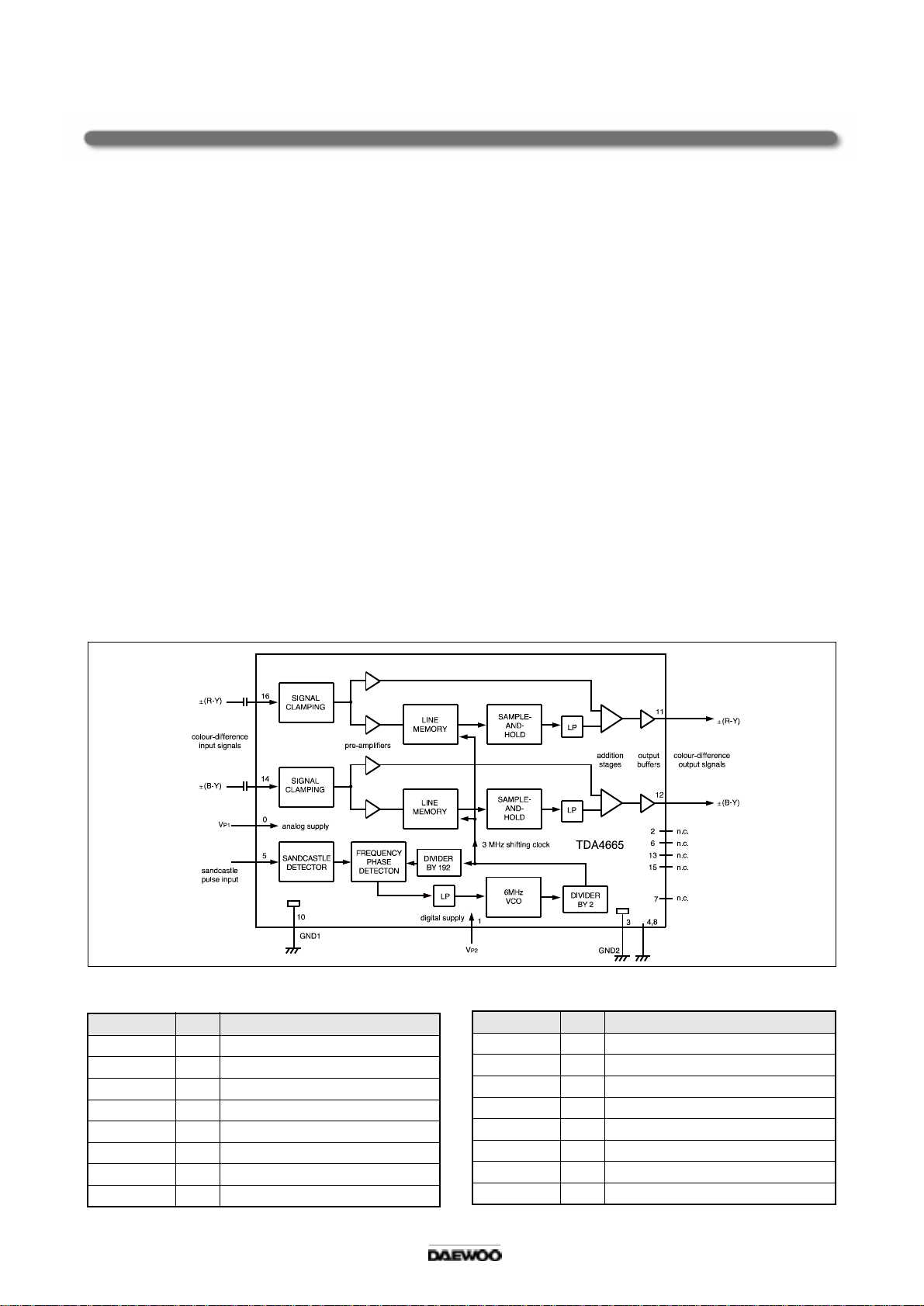
I502 TDA4665(Base Band Delay Line)
1. Features
• Two comb filters, using the switched-capacitor technique,for one line delay tim e (64µ s)
• Adjustment free application
• No crosstalk between S EC AM co lour carriers
• Handles negative or positive colour-difference input signals
• Clamping of A C-coupled input signals(±(R-Y) and ±(B-Y))
• VCO without external components
• 3MHz internal clock signal derived from a 6MH z VCO , line-locked by the sandcastle pulse (64µs line)
• Sample-and -hold circuits and low -pass filters to suppress the 3 M Hz clock signal
• Addition of delayed and non-delayed output signals
• O u tpu t b uffe r a m p lifiers
• Comb filtering functions for N TSC colour-difference signals to suppress cross-colour
2. General Description
The TDA4661 is an integrated baseband delay line circuit w ith one line delay. It is suitable for decoders
with colour-difference signal outputs ± (R-Y) and ± (B-Y).
3. Block Diagram
4. Pin Descriptio n
SYMBOL PIN DESCRIPTION
V
P2
1 +5V supply voltage for digital part
n.c. 2 not connecte d
GN D2 3 ground for digital part (
i.c. 4 internally connected
SAN D 5 sandcastle pulse input
n.c. 6 not connecte d
i.c. 7 internally connected
i.c. 8 internally connected
V)
SYMBOL PIN DESCRIPTIO N
V
P1
9 +5V supply voltage for analog part
GN D1 10 ground for analog part(
V
(R-Y) 11 ± (R-Y) output signal
0
V
(B-Y) 12 ± (B-Y) output signal
0
n.c. 13 not connected
V
(B -Y ) 1 4 ± (B-Y) inp u t s ign a l
1
n.c. 15 not connected
V
(R -Y) 16 ± (R-Y) inp u t s ign a l
1
21
V)
Page 24
I503 TDA8395 (Secam Decoder)
1. Features
• Fully integrated filters
• A lign m e n t free
• For use with baseband delay
2. Description
The TDA8395 is a self-calibrating,fully integrated SECAM decoder. The IC should preferably be used
in conjunction with the PAL/NTSC decoder TDA8362 and with the switch capacitor baseband delay
circuit TD A4665. The IC incorporates HF and LF filters, a demodulator and an identification circuit
(Ium inance is not processed in this IC).
A highly stable reference frequency is required for calibration and a two-level sandcastle pulse for
blanking and burst gating.
3. Block Diagram
BANDGAP TUNING TUNING
CVBS
16
ACC
INTERFACE
115
f
/IDENT
ref
4. Pin Descriptio n
SYMBOL PIN DESCRIPTION
fp1/IDE NT 1
reference frequency input/identification input
TEST 2 test output
Vp 3 positive supply voltage
n.c. 4 not connecte d
n.c. 5 not connecte d
GN D 6 ground
CLO CH Eref 7 C loche reference filter
PLL ref 8 P LL reference
ref
CLOCHE
100 nF
78362
CLOCHE
FILTER
CONTROL
SAND
220 nF
ref
PLL
PLL
IDENT-
IFICATION
GND
p
V
TDA8395
DE-
EMPHASIS
OUTPUT
STAGE
TEST
10
(R-Y )
9
(B-Y)
SYMBOL PIN DESCRIPTION
-(R -Y) 9 -(R-Y) outp u t
-(B-Y) 10 -(B-Y) output
n.c. 11 not connected
n.c. 12 not connected
n.c. 13 not connected
n.c. 14 not connected
SAN D 15 sandcastle pu lse input
CVB S 16 video(chrominan(e) input)
22
Page 25
I901, I902, I903 TDA6106Q ( Video Output Amplifier )
1. General Description
The TDA6106Q is a monolithic video output amplifier (5MHz bandwidth) in a SIL 9 MPpackage,
using high-voltage
DM OS technology, and is intended to drive the cathode of CRT directly .
To obtain maximum performance, the amplifier should be used with black-current control.
2. Feature
• Black - current measurement output for autom atic black current stabilization (ABS)
• Single supply voltage of 200V
• Internal protection against positive appearing CRT flash-over discharge
• Protection against E SD
• Inte rn al 2 .5 V refe re n ce circ u it
• Controllable sw itch-off behavior
3. Block Diagram
Pin 6
TDA61O6Q
Vdd
Vdd
MIR R O R 1
in out
MIRROR 3
Pin 9
Vof
Pin 3
vin
1XVbias 1X
DIFF.STAGE
out o u t out o u t
+
4. Pin Descriptio n
PIN SYMBOL DESCRIPTION
1N.C
2N.C
3 V in in v e rting inpu t
4 GND ground, substrate
5 I om B lack-current measurement output
6 V dd supply voltage high
7N.C
8 V oc ca thode output
9 V of feedback/transient output
Vdd
MIR R O R 2
out
Pin5
Ion
in
Pin 8
Voc
CURRENT
SOURCE
gnd
Pin 4
Gnd
in
23
Page 26

I804 PC817
1. General Description
The specification applies to the structures and characteristics of Model No. PC817
2. Block Diagram
3. Absolute maximum ratings
PARAMETER SYMBOL RATING UNIT
Input Forward current IF 50 m A
*1) Peak forward current IFM 1 A
Reve rse voltage VR 6 V
Pow er dissipation P 70 m W
Output Collector-em itter voltage VCE O 35 V
E mitte r-c o lle c to r v o lta g e VE CO 6 V
C olle cto r c urr en t IC 50 m A
Collector power dissipation Pc 150 m W
Total P ow er dissipation Ptot 200 mW
Operating temp erature Topr -3 0~ + 100
Storage temperature Tstg -55~ + 125
*2 ) I s o la tion v oltage V is o 5 kVrm s
*3) Soldering tem perature Tsol 260
C
C
C
*1) P ulse w idth100s, duty ratio: 0.001
*2) AC for 1 minute, 40~60% RH
*3) For 10 seconds.
24
Page 27

I301 TDA8356 (DC-coupled vertical deflection circuit)
1. General Description
The TDA8356 is power circuit for use in 90°C and 110°C color deflection systems for
field frequencies of 50 to 120 Hz.
The ci rcuit provides a DC driven vertical deflection output circuit, operati ng as a high efficient class G system.
2. Feature
• High efficient fully DC -coupled vertical output bridge circuit
• V ertic al fly -b ac k s w itc h
• Guard circuit
• Protection against : - short circuit of the output pins (7 and 4)
- sho rt circ u it of th e o u tp ut p in s to V p
• Temperature (thermal) protection
• High EMC imm unity because of common mode inputs
3. Block Diagram
4. Pin Descriptio n
PIN SYMBO L DESCRIPTION
1 I drive (pos ) input power stage (positive); include Ii(sb) signal bia s
2 I drive (neg ) input power stage (negative); include Ii(sb) signal bias
3 V p operating supply voltage
4 V o(b) output voltage B
5 GND ground
6 V fb input fly-back supply voltage
7 V o(a) output voltage A
8 V o(guard) guard output voltage
9 V I(fb) inpu t feedback voltage
25
Page 28

I604 LA4282
1. GENERAL DESCRIPTION
SIP-12H plastic package.
Function. Application : 2-Channel 10W AF Power Amp.
ITEM SYMBOL CONDITION RATED LEVEL UNIT
Recom m ended supply voltage VCC 32 V
Operationg supply voltage range VCC OP 10 TO 40 V
Recom m ended load resistance RL 8
2. Operation Conditions at TA=25
3. Pin Layout Diagram and Block Diagram
300
RIPPLE
FILTER
1
2 3 4 5 6 7 8 9 10 11 12
NF1 IN 1 RIPPLE
FILTER
PRE
GND
30K
-
CH1
+
-
CH1
+
300
NF2 OUT2 MUTE POWER
IN2
THERMAL
OVER VOLTAGE
PROTECTOR
MUTE
CIRCUIT
GND2
VCC
VCC
OUT1 POWER
26
Page 29

I603 PC 1406HA
1. General Description
PC1406HA is volume control IC with dual attenuator.
Contro curve of attenuator is linear for output
Channel separation is 64.0dB(MIN)
2. Block Diagram
3. Pin Descriptio n
INP U T 1
4
ATT
1
327
OUTPUT1
INPUT2 Vcc=12V
6
ATT
2
OUTPUT2
PC 1 406 HA
PC 1406H A
REGULATOR
8
1
5
9
1
12V
4. Electrical Characteristics at Ta=25
34
2
CONTROL1
C
°
5
678
AND
INP UT 1
OUTPUT1
INPU T 2
OUTPUT2
9
VCC
CONTROL2
ITE M SYMBOL RATED LEVEL UNIT
Recom m eded Supply Voltag e Vcc 0(MIN), 15(MAX) V
Input Terminal 4, 6 Signal V Vin 3 Vpp
Control T erminal 2, 8 V VC ON T 0(MIN), 15 (MAX ) V
Operated Temperature Topt -20 ~ +75
Allow able Power Dissipation PD 350(Ta=75
°C
QmV
Storage Ambient Temperature Tstg -40 ~ +125
27
°C
°C
Page 30

I504 (MM 1031XS)
1. MAKIMUM RATINGS (Ta=25°C
)
ITEM SYMBOL RATING UNIT
Storage Temperature Tstg -40 ~ +125
Oparating Tem perature Topr -20 ~ + 75
°C
°C
Supply Voltage VC CM A X 7 V
Pow ern Dissipation Pd 300 mW
2. ELECTRICAL CHARACTERISTICS
, Vcc=5.0V, unless otherwise indicated)
°C
ITEM SYMBOL TEST
(Ta=25
CONDITION MIN. TYP. MAX. UNIT
POINT
Supply Voltage Ran ge VC C VCC 4.7 5.0 5.3 V
Supply Current Id VCC 4.0 7.0 mA
Voltage Gain GV TP2 SI : Video sw eep signal
5.5 6.0 6.5 DB
1Vp-p, 0.1M H z
Frequency Response FC TP2 SI : Video Sw eep Signal
-1 0 1 DB
1Vp-p 7MHz/0.1M H z (*1)
Ouitput V oltage Sw ing Vop-p T P2 SI : Square wave
2.6 Vp-p
1.5Vp-p 16KHz
Differential Gain D G SO S I : S taircase 1Vp-p
13%
APL=10,50,90%
Differential Phase DP SO SI : STAIRCAS E 1V p-p
13DEG
APL=10,50,90%
Input Clamp Level Vc TP 1 2.0 V
(1) FREQUENCY RESPONSE FC
FC IS DECIDED FOLLOWING FORMURA
FC = 2 0L O G [ dB ]
V2
V1
V1 : A M P L IT U D E A T 0 .1MH z
V2 : A M P L IT U D E A T 7 M H z
3. Block Diagram
MM1031
12 3 45
+
470
SO
75
75 75
TP2 TP1
28
1
+
+
10
Vcc
SI
Page 31

I601, I602 (TC 4025 BP)
- DIFFERENTIAL 4-CHANNEL MULTIPLEXER/DEMULTIPLEXER.
in the case of V
can be switched from the logical circuit w ith signal pow er supply of 5 volts.
1. Absolute Maximum Ratings
CHARACTERISTIC SYMBO L RATING UNIT
DC Supp ly Voltage V
DC Supp ly Voltage V
Control Input Voltage V
Switch I/O Voltage V1/VO V
Control Input Current I
Potential Differen ce
Across I/O During ON
Power Dissipation PD 300(DIP)/180(SOP/SSOP) m W
Operation Tem perature Range TA - 40 ~ 85
Storage Temperature Range T
Lead temp. / Time T
= 5V VSS = 0V and VEE = -5V, signal betweem -5V And +5V
DD
DD
SS
DD
- V
- V
CIN
CIN
EE
- 0.5 ~ 20 V
- 0.5 ~ 20 V
VSS - 0 .5 ~ V
EE
- 0.5 ~ V
V1-V0 - 0.5 ~ 0.5 V
STG
SOL
- 6 5 ~ 15 0
260
DD
+ 0.5 V
DD
+ 0.5 V
10sec
mA
°C
°C
Truth Table
CONTROL INPUTS “ON” CHANNEL
INHIBIT C
LLLL00X, 0Y0X, 0Y, 0Z
L L L H 1 1X, 1Y 1X, 0Y, 0Z
L L H L 2 2X, 2Y 0X, 1Y, 0Z
L L H H 3 3X, 3Y 1X, 1Y, 0Z
LHLL4-0X,0Y, 1Z
LHLH5 -1X, 0Y, 1Z
LHHL6 -OX, 1Y, 1Z
L H H H 7 - 1X, 1Y, 1Z
H
: D on ’t C a re , : Except T C4052B
B A TC 4051B TC4052B T C4053B
NONE NONE NONE
29
Page 32

TC4052B
A
B
INH
10
1
0Y
2
Y2
3Y
1Y
3
4
5
6
7
EE
8
SS
16
Y-COM
INH
V
V
V
DD
9
6
LOGIC LEVEL CONVERTER
8
V
SS
7
V
EE
16
VDD
15
2X
14
1X
13
X-COM
12
0X
11
3X
10
A
9
B
X-COMMON
13
OUT c IN
OUT c IN
OUT c IN
OUT c IN
OUT c IN
OUT c IN
OUT c IN
OUT c IN
12
14
15
11
0X
1X
2X
3X
0Y
1
1Y
5
2Y
2
3Y
4
Y-COMMON
3
30
Page 33

I801 STR-S5707 (Hybrid IC for a Switching Regulator) : 2 speaker model
1. General Description
The STR-S5707 is a Hybrid IC with a built in power transistor and a separate excitation control IC,
designed for converter type switching mode power supply applications.
The IC is capable of quasi-resonant mode and requires small number of external component.
2. Feature
• Small SIP isolated package : Resin sealed type (transfer mold)
• Lower power dissipation at a lighter load
• Many protection function : - P ulse-by-pulse over current protection
- Over-voltage protection w ith a latch
- Thermal protection with a latch
• These protection functions are incorporated and can be latched with an external signal.
3. Block Diagram
4. Pin Descriptio n
PIN NAME SYMBOL DESCRIPTION
1 C olle c t o r C C o llec tor o f power T r
2 G round G N D ground (Emitter of power Tr)
3 B ase B B ase of power Tr
4 S ink SINK B ase current (IS) input
5 O ver-current protection OC P over-current sensing signal input
6 Inhibit Latch INH input for synchronizing OFF time and latch circuit operation
7 S ensing SEN S constant vo lta ge control signal input
8 D rive DR IVE Base drive current (ID ) output
9 V in V IN supply voltage for control circuit
31
Page 34

Electrical Characteristics of Control Part (Ta=25°C )
Description Terminal Sym bol
Rating
Unit
MIN TYP MAX
O n-s tate V o ltag e 9-2 VIN(ON) 7.6 8 8.4 V
Off-state Voltage 9-2 V
Operating Circuit C urrent 9-2 I
Stand-by Circuit Current 9-2 I
On Time
Off Tim e
OC P terminal Threshold Voltage 6-2 V
INH terminal Threshold Voltage 1 8-2 V
INH terminal Threshold Voltage 2 8-2 V
INH terminal Threshold Voltage 3 8-2 V
OV P O perating Voltage 9-2 VIN(Ovp) 9.2
Latch Circuit Sustaining C urrent 9-2 Ih
Latch Circuit Cancellation Voltage 9-2 V
MIC Therm al Shutdown
S ta rtin g Te mp
Fixed Reference Voltage 7-2 Vs
Tem perature Coefficient of
Reference Voltage
7-2
(Off) 4.6 4.9 5.2 V
IN
(O n ) 1 5
IN
IN
(Off)
TON 33
T
Off
OCP
INH-1
INh-2
LATCH
IN(La.O FF)
45
-1.1 2 - 1 - 0 .8 8 V
0.65 0.75 0 .85 V
3.2 5.1 5.8 V
2.5 3.1
Tj(TSD ) 125 150
28 mA
200
41
55
1.4 2..0 V
10.7 V
500
+ 2.5
0.3
32.0
mV/
A
sec
sec
A
V
V
°C
Electrical Characteristics of Power Transistor Part (Trl) (Ta=25°C )
Description Terminal Sym bol
Collector S aturation Voltage 1-2 V
Collector Cutoff Current 1-2 I
Base-Em itter saturation voltage 3-2 V
DC Current Gain
Thermal Resistan ce
CE
BE
h
(sat)
CEX
(sat)
FE
-F
S wit c h in g Time 1 - 2 ts
1-2 tf
Ra tin g
MIN TYP MAX
29
0.4 V
100
1.5 V
61
1.3
15
0.5
Unit
°C
/w
sec
32
Page 35

I802 TDA8138 (5.1V+12V regulator with Disable and Reset)
1. General Description
The TDA8138 is a monolithic dual positive voltage regulator designed to provide fixed precision output
voltages of 5.1V and 12V at currents up to 1A.
A internal r eset cuicuit generates a reset pulse when the output 1 decrease below the regulated voltage value.
Output 2 can be disabled by TTL input.
Shot circuit and themal protections are included.
2. Feature
• ou tp ut c u rre nts u p to 1 A
• ixed precision Output 1 voltage 5.1V
• fixed precision Output 2 voltage 12V
• ou tp ut 1 w ith R e se t fa cility
• output 2 with D isable by TTL input
• short circuit protection at both outputs
• the rm a l p ro tec tio n
• low d ro p ou tp ut v o ltag e
3. B lo c k Dia g ra m 4. P in De s c rip tio n
2%
2%
PIN SYMBOL DESCRIPTION
1 V in 1 input 1
2 V in 2 input 2
3 C e Delay capacitor
4 V d is d isab le
5 GN D ground
6RST reset
7n.c
8 V out 2 output 2 (12V)
9 V out 1 output 1 (5.1V)
33
Page 36

PCA84C 122A(IC REMOCON)
1. Features
• ROM, RAM and I/O is device dependent
• Two test inputs T0, T1
• 3 Single-level vectored interrupt sources
• 8 b it pr og ra m mab le timer/c o un te r w ith 5 -b it p re-s c ale r
• Single supply voltage from 2.0V to 5.5V
• On-board oscilla to r 1 MH z to 5 MH z
• Operating temperature range -20 to +50°C
2. General Description
The PCA84C 122A is a stand-alone m icro controller designed for use in rem ote control unit for a wide
range of applications.
3. Pin Descriptio n
Pin Signal de s c riptio n
3P00
2P01
23 P02
22 P03
10 P04
11 P05
14 P06
15 P07
19 P10
18 P11
17 P12
16 P13
1P14
24 P15
12 P16
13 P17
4 T P / IN T T e s t T0 an d e x te rn a l in te r ru p t in p u t
5T1Test T1
6 R ESET Ac tiv e HIG H res e t , n o rmally tie d to Vs s b e c a us e in te r n a l
8XTAL 1
9XTAL 2
21 OUT Pu lse train output pin, capable of sinking 27mA
7V
20 Vss Ground
DD
Standard I/O P ort lines, generally used for keypad scanning
Standard I/O P ort lines, generally used for keypad scanning
Powe r-on re set can serve the same function
Crystal or ceramic resonator
Powe r supply
34
Page 37

6. CIRCUIT DESCRIPTION
6-1. Vision IF amplifier, AFC, video demodulator
The IF signal from the tuner is fed through a SAW filter to the differential IF input (pin 48 and 49).
The first IF stage consists of 3 AC-coupled amplifiers with a total gain control range of over 66 dB.
The reference carrier for the video demodulator is obtained by a PLL carrier regenerator
(eliminating notch filter compromises, as in reference tuned circuits for passive carrier regeneration).
O n ly a n o s c illa to r c o il is n eeded( pin 3 and 4) that can be aligned via l2C-bus to the double IF frequency.
The AFC information is derived from the VCO control voltage of the IF-PLL and can be read via I2C-bus.
Bit A FB toggles when the picture carrier is exactly at the desired IF frequency
(= half the aligned IF-PLL frequency).
AFA is active in a w indow around this point.
For f ast searc h-tuni ng appli cations this window can be i ncreased by a f actor 3 ( AFW bit) .
6-2. Tuner A.G.C.
The automatic gain control (A.G.C.) circuit operates on top sync level at negative modulated signals
or on peak white level at positive m odulation, selected by MOD bit.
The tuner A.G.C. is controlled via pin 54.
The tuner A.G.C. take over point (T.O.P.) can be set over a w ide range: 0.8 mV rms .. 80 m Vrms
IF input signal am plitude.
The tuner AG C output m ay have to operate above Vcc of TDA8374.
Therefore pin 54 is an open collector output, that can operate from 0.3 up to Vcc+ 1 Volt
(at > 2 m A sink current)
6-3. PLL sound demodulator
The IF-video output at pin 6 (2Vpp) is fed through a sound bandpass filter and connected to the intercarrier
sound IF input pin 1.
An alignm ent free PLL tunes itself to the sound carrier and demodulates it.
The non volum e-controlled front-end audio signal can be obtained from the deemphasis pin 55
(amplitude 300 mVeff).
6-4. Source select switch
TDA8374 input sw itch can select one of the following sources ;
pin 13 front-end : C VBS l int
pin17 : CVBS 2 ext
pin 11.pinlO : Y s-vhs, C s-vhs
Selected signal is available at the CVBS output pin 38, in case of Y/C input Y+C are added.
It drive teletext and the TDA8395 SEC AM add-on.
For S-VHS applications, the Y,C input can be selected, independent of the CVBS source switch.
TDA8374 Y,C inputs are selected, while the source switch outputs CVBS l int or C VBS 2 ext on CVBS out.
35
Page 38

6-5. Horizontal synchronization and protection
The synchronization separator adapts its slicing level in the middle between top-sync and black level of the CVBS signal.
The separated synchronization pulses are fed to the first phase detector and to the coincidence detector.
The
The coincidence detector detects whether the horizontal line oscillator is synchronized to the incoming video.
The line oscillator is a VCO -type, running at twice the line frequency.
It is cal ibrat ed wi th the X-t al oscillat or frequency of the col our de coder and has a maximum devi at ion of 2% of t h e
nominal frequency, so no alignm ent is-needed.
Calibration is done at start up( the TDA8374 m ust first know what colour X-tals are connected,
bits XA and XB ) and after synchronization loss (
The second phase detector
horizontal flyback pulse at input pin 41.
This compensates for the storage time of the horizontal deflection transistor.
The
The horizontal phase can be given a static off set via I2C-but (HSH “horizontal shift”)
A dynamic correction is possible by current feedback into the
To protect the horizontal deflection transistor, the horizontal drive is switched off imm ediately when a power
failure ( “ P o w e r-On R e s et “ b it P O R ) is de te c ted .
The power failure m ay have corrupted the contents of the internal data registers, so the TDA8374 should be
started up again.
-1 loop gain is determined by the components at pin 43 (C+RC).
-1 coincidence detector “Sync Locked” bit SL).
-2 locks the phase of the horizontal driver pulses at output pin 40 to the
- 2 loop filter (C) is externally connected to pin 42.
- 2 loop filter capacitor.
The TDA8374 has a separate supply input (pin 37) that only used as a clean supply voltage for the horizontal
oscillator circuits.
6-6. Vertical synchronization
The vertical saw tooth generator drives the vertical output.
It uses an external capacitor at pin 51 and a current reference resistor at pin 52.
The TDA8374 vertical dr ive has differential current outputs f or DC-coupl ed v ertical output s tage, like the TDA8356 .
At TDA8356 input pins l and 2 this current is converted into a drive voltage via a resistor.
6-7. Geometry processing
W ith the TDA8374 is possible to im plement automatic geometry alignm ent, because all parameters
are adjusted via the I2C bus.
The deflection processor of the TDA8374 offers the following five controls;
- Horizontal shift
- Vertical slope.
- Ve rtic al a m p litud e
- Vertical S-correction
- ve rtica l sh ift
36
Page 39

6-8. Colour decoder
The colour decoder contains an alignment-free X-tal oscillator, a dual killer circuit and colour difference
demodulators.
Together w ith the TDA8395 SEC AM add-on a multi standard PAL/SECAM /NTSC decoder can be built with
automatic recognition.
W hich standard can be decoded depends on the external Xtals used.
Two Xtal pins (34and 36) are present so normally no external switching is required.
The I.C . must be told which X-tals are connected (bits XA and XB).
This is important, because the X -tal frequency of the colour decoder is also used to calibrate many internal circuit.
The burst phase detector locks the X tal oscillator with the chroma burst signal.
The phase detector operates during the burst key period only , to prevent di sturbance of the PLL by the chroma signal.
Two gain modes provide:
- Good catching range when the PLL is not Locked.
- Low ripple voltage and good noise imm unity once the PLL has locked
The killer circuit switches-off the R-Y and B-Y demodulators at very low input signal conditions (chroma burst amplitude).
A hysteresis prevents on/off switching at low, noisy signals.
Color standard pin34 pin35 XA XB
PAL4.43/SECA M + N TSC -4.43 none 4.43 1 0
PAL4.43/SECA M + N TSC -M 3.58 4.43 1 1
6-9. Integrated video filters
The TDA8374 has alignm ent-free internal luminance delay, chroma bandpass and chroma trap.
They are im plemented as gyrator circuits tuned by tracking to the frequency of the chroma Xtal oscillator.
The chroma trap in the Y signal path is by-passed when Y/C input is selected (S-VHS ).
For SECAM an extra lum inance delay is build-in, for correct delay of the luminance signal.
6-10. RGB output and black current stabilization
The colour difference signals (R-Y, B -Y) are matrixed with the luminance signal (Y) to obtain the RGBout
output signals (pins 21,20,29).
In the TD A8374 the matrix type automatically adapts to the decoded standard (N TSC,PAL) .
Linear am plifiers are used to interface external RG B signals (pins 24,25,26) from the SCAR T connector.
These signals overrule the internal R GB signals when the data insertion pin 26 (FBI) is switched to a level
between 1.0V and 3.0V.
The contrast and br ightness control and the peak white limit er ope r ate on both i nternal and external RGB signals
R,G and B each have their own, independent gain control to compensate for the difference in phosphor
efficiencies of the picture tube: so called “white point” adjustment.
The nominal am plitude is about 2V black to white, at nom inal input signals and control settings.
37
Page 40

TDA8374 has a black current stabilization loop, that automatically adjust the black level to the cut-off voltage
of the picture tubes three gun cathodes.
Since no current is flowing when the voltage the cathode is equal to the cut-off voltage of the tube, the loop
stab iliz e s a t a v e ry s mall g u n c u rr e n t.
This “black current” of the three guns is measured internally and compared with a reference current, to adjust
the black level of RGB out.
The black level loop is active during 4 lines at the end of the vertical blanking.
In the first line the leakage current is measured (m ax. acceptable 100
In the next three lines the black levels of the three guns are adjusted.
The nominal value of the ‘black current is 10
The ratio of the ‘black currents’ for the 3 guns tracks automatically with the white point adjustment, so the
back-ground colour is the same as the adjusted white point.
At switch-on of the TV receiver the black current stabilization circuit is not yet active and RGBout are blanked.
Before the first measurement pulses appear, O.5 sec delay ensures that the vertical deflection is active,
so the pulses will not be visible on the screen.
During the measuring lines RGBout will supply 4V pulses to the video output stages.
The TDA8374 waits until the black current feedback input (pin 18) exceeds 200
the picture tube is warm-up.
Then the black current stabilization circuit is active.
After a waiting tim e of about 1.0 sec, the blanking of RGBout is released.
.
).
, which indicates that
6-11. Tuning
The AFC information of the TDA8374 is not available as an analogue voltage.
Automatic following (=frequency tracking, AFC) can be done via the I2C-bus by software.
The TDA8374 AFC window is typically 80 kHz wide.
This value is made higher than the 62.5 kHz tuning step, to prevent an automatic following loop from
continuously adapting the tuning frequency.
W ith this A F C w in do w (
For high speed search-tuning-algorithms, the AFC window can be widened to 240 kHz via bit AFW .
40 kHz) the m aximum tuning error is less than 62.5 kHz.
6-12. TDA8395 SECAM decoder
The TDA8395 is an alignment-free SECAM colour decoder, including a Cloche filter,
demodulator and line identification circuit.
The Cloche filter is a gyrator-capacitor type.
Its fre q ue n cy is c a libra ted in th e v e rtica l retra c e pe rio d.
The calibration reference( pin 1 ) is obtained from the TDA8374 color X-tal oscillator (p in 3 3 ).
Pin 7 is a decoupling for the Cloche reference.
The voltage change at this pin due to leakage currents should be low er than 10 mV, during field scan,
resulting in a capacitor of m inim al 100nF.
38
Page 41

Pin 8 is the reference capacitor for the PLL.
The voltage variation during field scan at this pin should be lower than 2 mV , resulting in a capacitor of 220
The sandcastle input (pin 15) is connected to TDA8374 pin 41 and is used for generation of the blanking
periods and provides clock inform ation for the identification circuit.
The CVBS source select output (TDA8374 pin 38) supplies SECAM chroma to pin 16 of the TDA8395.
This is demodulated by a PLL demodulator, that uses the reference frequency at pin l and a bandgap
reference to obtain the desired demodulation characteristic.
If the digital line identification in theTDA8395 detects SECA M, pin 1 will sink a current of 150
(A out of TDA8374 SE CAM ref pin 33.
When the TDA8374 has not det ected PAL or NTSC, i t wi ll r espond by increasi n g t he vo ltage at pin 33 from 1. 5V t o 5V.
Now the TDA8374 color difference outputs pin 30 and 29 are made high-ohmic and the TDA8395 output pin
9 and 10 are switched on.
These outputs will be disconnected and high-ohmic when no SECAM is detected for two frame periods,
the decoder will be initialized before trying again.
.
6-13. Base band delay line TDA4665
TDA4665 is an integrated double baseband delay line of 64S.
It couples to the TDA8374 and TDA8395 w ithout any switches or alignm ents.
The TDA4665 consist of two main blocks:
- Two delay lines of 64 sec in switched capacitor technique
- Internal clock generation of 3 MH z, line locked to the sandcastle pulse
The TDA4665 operates according to the m ode demanded by the colour transmission standard:
- For P AL it operates as geometric adder to satisfy the PAL dem odulation requirements
- In N TSC m ode it reduces cross-colour interference (comb-filtering)
- For S ECA M it repeats the colour difference signal on consecutive horizontal scan lines.
A sandcastle pulse is connected to pin 5.
The top pulse vol tage (should not excee d 5 V) can be d irect ly coupled t o the 5 V sandcastle output of the TDA8374.
The R-Y and B-Y colour difference signals (from TD A8374 pins 30 and 29) are AC-coupled and clamped by
the input stages at pins 16 and 14.
An internal 6 MH z Current controlled oscillator is line locked via a PLL to the sandcastle pulse at pin 5.
This clock drives the delay lines to obtain the required 64
Sam ple and hold low pass filters supress the clock signal.
The original and the delayed signals are added, buffered and fed to the output pins 11 and 12.
These are AC-coupled to the R-Y and B-Y colour difference input pin 32 and 31 of TD A8374.
The TDA4665 needs a 5 V supply voltage on pin 1 for the digital part and on pin 9 for the analog part.
sec.
39
Page 42

6-14. TDA8356 vertical deflection.
The TDA8356 is a vertical deflection circuit.
It can be used in 90° deflection system s with frame frequencies from 50 up to 120 Hz
W ith its bridge configuration the deflection output can be DC coupled with few external components.
Only a supply voltage for the scan and a second supply for the flyback are needed.
The TDA8356 can drive m ax.2A.
The vertical drive currents of TDA8374 pins 47 and 46 are connected to input pins 1 and 2 of the TD A8356.
The currents are converted into a voltage by a resistor betw een pins 1 and 2.
Pin2 is on a fixed DC level (internal bias voltage) and on pin 1 the drive voltage can be measured (t ypic al 1.8 Vpp).
The drive voltage is amplifi ed by ‘A’ and f ed to two amplifier s ‘B’ and ‘C’, one is inver ting and t h e other i s a no n
inverting amplifier.
The outputs (pins 4 and 7) are connected to the series connection of the vertical deflection coil and
feedback resistor.
The voltage across feed back resistor is fed via pin 9 to correction amplifier ‘D’, to obtain a deflection current
which is proportional to the drive voltage.
The supply voltage for the TDA8356 is 16V at pin 3.
The flyback generator has a separate supply voltage of 45V on pin 6.
The guard pulse is useful to synchronize OS D.
6-15. Horizontal deflection
The circuit contains horizontal drive, line output transformer.
The horizontal driver pulses from the TDA8374 are amplified in the horizontal drive circuit, to get sufficient
base-drive current for the high voltage switching transistor Q401.
During the horizontal scan period( =52
through the prim ary winding of the FBT to ground.
After this time Q 401 is switched off and the energy stored in the FBT during the scan period will be
transformed to the flyback capacitor C410.
This energy t r ansf er will take pl ace i n a cosi ne shape because the pri mary of t he FBT and C410 fr om a resonant cir cuit.
The tim e the energy is transferred from FB T to C410 and back to the FBT, is called the flyback time and will
take place in about 12
The flyback peak voltage is about 8 times the scan voltage.
In series with the horizontal deflection coil there is a (damped) linearity corrector coil.
During the scan there is some loss in the resistance of the deflection coil.
In the first part of a line the linearity corrector stores some energy in a permanent magnet until it is saturated.
This improves the linearity of the horizontal scan speed.
The required S correction for the picture tube can be adjusted with the value of C411.
s.
s) Q4 01 will conduct, and a sawtooth current flows from +110/123V
40
Page 43

The beam current limiting inform ation (BeamCurr) is derived from the foot of the H.V winding of the FBT.
This is connected via resistor to +8V.
As the beam current increase, the voltage on line BeamCurr decreases.
BeamC urr is damped by a integration filter before it is fed back to TDA8374 pin 22.
The TDA8374 will decrease the contrast (and eventually the brightness) to limit the average beam current.
6-16. Video amplifiers
Three TDA6106Q integrated video amplifiers drive cathode of the picture tube directly.
They are protected against CRT flashover discharges and ESD (electro static discharge).
The three video amplifiers, have a beam current output I black, used by the TDA8374 black current loop to
control the black level on the cathodes.
The outputs can be connected together because the black current loop sequentially controls the black level
for each cathode.
The amplification of the TDA6106Q is set by the resistors between pin 3 and 9 and between pin 3
(negative-input) and the TDA8374 output.
There are no alignment any more on the CPT panel, because of the automatic black current stabilization and
because the w hite point adjustment can be done in the TDA8374 via I
2
C bus.
6-17. Power Supply STR-S5707
1. VIN terminal, start-up circuit
A start-up circuit is to start and stop a operation of a control IC by detecting a voltage appearing at a VIN
term inal (pin-9 ).
At start up of a power supply, when a voltage at the VIN terminal reaches to 8V (typical) by charging up C807
by the functi on of a start-up resi s tor, R803, a control circui t starts operating by the function of t he start-up circuit.
After the control circuit starts its operation, power source is obtained by smoothing voltage appearing at
winding of pin6-7 of T801.
2. O s c illa to r , F /B te rmin a l v olta g e (P in 7 )
A oscillator generates pulse signals which turns a power transistor on and off by making use of charge and
discharge of C1 and C2 incorporated in the Hybrid IC.
Constant voltage control of a switch-mode power supply is performed by changing both ON-time and O F Ftim e except when the load is light (ex. remote control stand-by mode of TVs).
The ON-time is controlled by changing a current charged by C1, which is as the result of that the detection
winding of pin5-7 of T801, which detects a ch ange of voltage in a secondary side, connected to the s en s ing
terminal (Pin 7) has the current in accordance with an output signal from an output voltage detection circuit
(an error amplifier) built in.
As an AC input voltage to the power supply gets the higher and a load current the smaller, the current
flowing to the SENS terminal gets the larger, and the O N-tim e gets the shorter.
41
Page 44

3. Functio n of INH terminal (Pin 6), control of OFF-time
S ign al to th e IN H termin a l is u se d a s in pu ts to C OM P .1 an d C O MP.2 in sid e of th e co n tro l IC.
A threshold voltage of COMP.1, VTH1 is set at 0.75V (Ta=25°) and an input signal to a drive circuit becomes
almost 0V (the power transistor is in O FF m ode) when a voltage at the IN H terminal reaches the VTH1.
A threshold voltage of COMP.2, VTH2, is set at 1.5V (Ta=25°).
When the INH terminal voltage reaches VTH2, an output from COM P .2 reverses
(the power transistor is in on mode).
Quasi-resonant operation
By inputting the voltage of winding of pin6-7 of T801 w hich is synchronized with the energy discharge
tim e of a secondary winding, pin14(or 15)-16 of T801, to the INH terminal through D805 and R 809,
quasi-resonant operation can be achieved.
When the power transistor turns off and a voltage higher than VTH2 is applied to the INH terminal,
C3 immediately discharges and then starts charging again.
Even after the discharge of energy of a secondary winding is completed,
VINH does not immediately increases.
When it gets lower than VTH1, the transistor turns on.
Stand-By Mode
While being in remote control stand-by mode, the output voltage is kept on providing to the secondary side
and the power transistor operates at A class m ode.
By connecting INH term inal (Pin 6) to the GND, the OFF-tim e of the pow er transistor is fixed at set time
( T O F F = 5 0 u s e c a t T a = 2 5 °C ) o f th e b u ilt-in o s c illa to r , a n d o n ly O N- time c h a n g e s d e p ending on input
and output conditions of the power supply.
The r e fo re , it e n a b le s to h o ld a n o s c illa tio n fre q uency in light mode below 20KHz (typical).
4. Drive circuit
The STR-S5707 applies the proportional drive system in order to minimize turn-on and saturation loss,
and storage time.
5. OCP (over-current protection) function
Over- current p r ot ec t ion is per formed pulse by pu l s e by direct l y detecti ng c ollect or current of the power t r ans i s t or .
Detecting voltage is set to -1V below a reference point of G ND (ground).
6. Latch circuit
It is a circuit whi ch sustains an out put from the oscillator low and stops operation of the power supp ly when
over-voltage protection (OVP ) circuit and therm al shutdow n (TSD) circuit are in operation.
As the susta ining current of the latch circuit is 500
supply circuit sustains the off state as long as current of 500
maximum when VIN terminal voltage is 4V, the power
m in im u m flo w s to V IN te rminal fro m
a start-up resistor.
42
Page 45

In order to prevent a m alfunction to be caused by a noise and so on, delay time is provided by C1
inc orporate d in the IC and, therefore, the l atch cir c u it opera tes when t he OVP or TSD circuit is in operat ion,
or an external signal input is provided for about 10
sec or longer.
In addition, even after the latch circuit start operating, the constant voltage regulator(Reg) circuit is in
operation and the circuit current is at high level.
As a result, VIN terminal voltage rapidly decreases.
When V IN terminal voltage becomes lower than the shutdow n voltage, VIN(OFF) (4.9V typical),
it starts increasing as the circuit current is below 500
.
When it reaches the ON-state voltage, VIN (ON) (8V typical), VIN terminal voltage starts decreasing be
cause the circuit current increase s again.
When the latch circuit is on, VIN terminal voltage increases and decreases within the range from 4.9V
typical to 8V typical and is prevented from abnormally rising.
Cancellation of the latch is done by decreasing VIN term inal voltage below 3.3V.
The power supply can be restarted after disconnecting an AC input to the power supply once.
7. Thermal shutdown circuit
It is a circuit to trigger the latch circuit when the frame temperature of the IC exceeds 150°C (typical).
Although the temperature is actually sensed at the control chip, it works against overheating of the power
transistor as the power transistor and the control IC are mounted on the sam e lead fram e.
8. Over-voltage protection circuit
It is a circuit to trigger the latch circuit when VIN term inal voltage exceeds 11V (typical).
Although it basically functions as protection of VIN terminal against over-voltage, since VIN terminal is
usual ly supplied fr om the drive winding of t he t ransformer and the voltage is pr oportional to t he o ut put volt age,
it also functions against the over-voltage of secondary output which causes when the control circuit opens or
in some other events.
43
Page 46

7. PCB LAYOUTS
7-1. PRINTED CIRCUIT BOARDS
44
Page 47

45
Page 48

Page 49

8. TROUBLE SHOOTING CHARTS
8-1. NO RASTER
CHECK MAIN B+(+123V+110V)LINE
N.G.
CHECK VOLTAGE AT
(+) OF C806(220µF 450V)
310Vdc AT AC 220V
N.G.
CHECK/REPLACE F801
FUSE(T4A 250V)
CHECK/REPLACE
D801~D804(1S1888X4)
R803(10W 3.3OHM)
CHECK POWER SWITCHING
VOLTAGE AT PIN 43 OF I701
*POWER ON : HIGH
*STAND-BY : LOW
O.K.
CHECK/REPLACE
I801(STR-S5707)
& PERIPHERAL
COMPONENT
CHECK/REPLACE
I804(PC817)
D812(BYW 95C)
R814(2W56K)
CHECK/REPLACE
I802(TDA8138)
I803(KA7808)
O.K.
CHECK HEATER VOLTAGE,
VIDEO B+(200V) LINE,
16.5V & 48V LINE
N.G.
CHECK HORIZONTAL
DRIVE PULSE AT PIN
OF I501(TDA8374A)
[REFER TO WAVE
FORM 20]
N.G.
CHECK HORIZONTAL
CC
V
(+8V DC) AT
PIN 37 OF I501
N.G.
CHECK SDA(PIN 8)
& SCL(PIN 7)
WAVEFORM OF I501
O.K.
O.K.
CHECK/REPLACE
R410(1/4W 3.9)
Q401 (2SD1207)
T401 (HD-15D)
Q402 (2SD2499)
O.K.
O.K.
CHECK VOLTAGE(+5V DC)B+
AT PIN 11 & PIN 3 7 OF I701
CHECK SDA(PIN 3)
WAVEFORM OF I701
CHECK/REPLACE
N.G.
O.K. N.G.
& SCL(PIN 4)
X701(20MH
Z
)
N.G.
CHECK/REPLACE
D813 (BYV95C)
D814 (BYV95C)
R824 (2W 43)
Q802 (KTC 3198Y)
Q80 (KTC 3198Y)
T801(TSM-4445A5)
O.K.
CHECK/REPLACE
I701
46
CHECK/REPLACE
I501(TDA8374A)
CHECK/REPLACE
T402 F.B.T & CRT
O.K
Page 50

8-2. NO PICTURE(RASTER OK)
AT PIN 13 OF I501(TDA8374A)
[REFER TO WAVEFORM 3]
CHECK VIDEO SIGNAL
N.G.
CHANGE INPUT MODE
→ AV → RF
RF
N.G.
CHECK PICTURE
CONDITION
NORMAL 1, NORMAL 2
FAVOURITE
O.K.
CHECK TUNING
VOLTAGE
AT VT OF TUNER
O.K.
CHECK BAND SELECT
VOLTAGE AT BL,BH,BU
& B+ VOLTAGE
OF TUNER
N.G.
N.G.
O.K.
CHECK/REPLACE
I701
& PERIPHER AL
COMPONENT
CHECK/
REPLACE
Q702, Q703
CHECK 33V LINE
N.G.
CHECK/
REPLACE
R726, R720
I703
N.G.
N.G.
CHECK WAVEFORM AT
PIN 29 PIN 30 OF I501
O.K.
CHECK WAVEFORM
AT PIN 31 PIN 32
OF I501
O.K.
CHECK WAVEFORM
AT PIN 19, 20, 21
OF I501
O.K.
CHECK VIDEO SIGNAL
AT CATHOD OF CRT
[REFER TO WAVEFORM
15, 16, 17]
O.K.
O.K.
N.G.
CHECK/REPLACE
I501
N.G.
CHECK/REPLACE
I502(TDA4665)
14, 16, 11, 12
I503(TDA8395)16, 9, 10
N.G.
CHECK SIGNAL
AT PIN 18 OF I501
N.G.
N.G.
O.K.
CHECK/REPLACE TUNER
CHECK/REPLACE
Q101, Q102, SF101
CHECK/REPLACE
I501
CHECK/REPLACE
AT PIN 40, 41, 42
CHECK/REPLACE
Q705, Q706, Q707
O.K.
Q708, Q709, Q710
OF I701
O.K.
CHECK/REPLACE
I901, I902, I903
(CRT BOARD)
O.K.
47
O.K.
CHECK/REPLACE
CRT
O.K CHECK
CHECK VOLTAGE
VIDEO B+,
HEATER
N.G.
HORIZONTAL
CIRCUIT PARTS
Page 51

8-3. NO VERTICAL SCANING(ONE HORIZONTAL LINE ON SCREEN)
CHECK / REPLACE
P401 & DY
CHECK VERTICAL Vcc
+16.5V AT PIN3
& +48V AT PIN 6
OF I301(TDA 8356)
N.G.O.K.
CHECK SIGNAL
AT PIN1 & PIN2
OF I301 [REFER TO
WAVEFORM 18, 19]
CHECK / REPLACE
D401(BYV95C)
D409(BYVC95C)
R303(1W 15K)
CHECK / REPLACE
CRT
O.K.
O.K.
CHECK SIGNAL
AT PIN7 OF I301
WAVE FORM 8
CHECK / REPLACE
R304, R305
R304, R307
N.G.
CHECK OUTPUT
WAVEFORM AT PIN 46
PIN47 OF I501
O.K.
CHECK / REPLACE
I301
OK
N.G.N.G.
CHECK / REPLACE I501
48
Page 52

8-4. NO COLOR
CHECK VIDEO SIGNAL
AT PIN 13 OF I501(TDA8374A)
[REFER TO WAVEFORM ]
O.K.
CHECK SYSTEM MODE
AUTO
PAL SECAM
N4 N5
N3
CHECK SIGNAL
AT PIN 29, PIN 30
OF I501
O.K.
CHECK/REPLAC E I501
CHECK SIGNAL
AT PIN 31, PIN 32
OF I501
O.K.
CHECK SINAL
AT PIN 19, 20, 21
OF I501
N.G.
NO PICTURE CHART
N.G.
CHECK / REPLACE
X501(4.43MHz X-TAL) I501 35
X502(3.58MHz X-TAL) I501 34
N.G.
CHECK / REPLACE
I503 16, 10, 9
I502 14, 16, 11, 12
REFER TO
O.K.
CHECK VIDEO SIGNAL
AT CATHOD OF CRT
[REFER TO WAVEFORM
15, 16, 17
O.K.
CHECK / REPLCE
CRT
OK
N.G.
CHECK / REPLACE
I501
N.G.
CHECK / REPLACE
I901, I902, I903(TDA 6106Q(R, G, B)
(CRT BOARD) #3, #5, #9
49
Page 53

8-5. NO SOUND(PICTURE OK)
CHECK AUDIO SIGNAL
AT PIN 55 I501
CHECK MUTE VO LTAGE
AT PIN20 OF I701
*MUTE : HIGH
N.G.
N.G.
CHECK AUDIO SIGNAL
AT PIN I603 #3, #7
O.K.
CHECK VOLAGE
Vcc(12V)
AT I603 #1
O.K.
O.K.
N.G.
CHECK/
REPLACE
R620, 621, 622, 625
C 614, 615, 617, 618
O.K.
CHECK SIF SIGNAL
AT PIN1 OF I501
O.K.
CHECK / REPACE I501
CHECK AUDIO SIGNL
AT PIN LA4282 #2 #5
O.K.
CHECK VOLTAGE Vcc(+32 Vdc)
AT PIN LA4282 #10
O.K.
CHECK AUDIO
OUTPUT SIGNA
AT PIN7, 11(LA4282)
N.G.
CHECK / REPLACE
RA08, QA02
CA04, RA15
N.G.
CHECK SIGNAL WAVEFORM
AT PIN6 OF I501
[REFER TO WAVEFORM
O.K.
CHECK / REPLACE
Q501, R602, R603
Q605 & PERI. COMP
N.G.
CHECK / REPLACE
TUNER, SAW FILTER
Q101, Q102 & PERI, COMP
CHECK AUDIO
SIGNAL AT
PIN I603 #4, #7
CHECK /
REPLACE
I602 (TD 1405BP)
O.K.N.G.
CHECK /
REPLACE I603
(UPC14406HA)
O.K.
CHECK / REPLACE
(SP01&SP02)
C620, 621, 622, 623
R626, 627, 628, 629
OK
N.G.
CHECK MUTE VOLTAGE
AT PIN 3 OF I601
MUTE: LOW
N.G.
CHECK / REPLACE
Q602, 612, R631, C626
50
R619, D712
O.K.
CHECK / REPLACE
I602 LA4282
C613, 624
Page 54

8-6. NO EXTERNAL A/V(RF OK)
CHECK EXTERNAL
VIDEO AT PIN 17
OF I501
CHECK WAVEFORM
AT PIN 7 & 8 OF I501
CHECK / REPLACE
I701
CHECK WAVEFORM
AT PIN 14 & 15 OF I601
N.G.
CHECK WAVEFORM
O.K.
O.K.N.G. O.K. N.G.
CHECK / REPLACE
I501
OK
CHECK EXTERNAL AUDIO
AT PIN 14 & 15 OF I602
O.K.
CHECK RCA
AT PIN 3 & 5 OF I601
JACK
CHECK VOLTAGE
AT PIN 16 OF I602
O.K.
CHECK VOLTAGE
AT PIN 16 OF I601
CHECK / REPLACE
I601
CHECK WAVEFORM
AT PIN 1, 2, 12, 13
OF I601
CHECK RCA
JACK
CHECK VOLTAGE
AT PIN 16
OF I601
CHECK / REPLACE
I601
CHECK / REPLACE
I602
51
Page 55

8-7. NO ON-SCREEN DISPLAY(PICTURE OK)
CHECK HORI. & VER. SYNC
AT PIN 46 & 45 VS, HN(IN)
OF I701 RESPECTIVELY
CHECK HORI. & VER. SYNC
AT PIN 46 & 45 VS, HN(IN)
OF I701 RESPECTIVELY
N.G.
CHECK / REPLACE
PERI.COMP
N.G.
CHECK WAVEFORM
AT PIN 23, 24, 25, 26
OF I501 RGB(IN) BL
O.K.
CHECK / REPLACE I501
O.K.
O.K.
O.K.
CHECK OSD R/G/B SIGNAL
& BLANKING SIGNAL
AT PIN 47, 48, 49 & 50 OF I701
R, G, B(OUT) BL
CHECK OSD IN/PUT WAVEFORM
AT PIN 38, 39 OF I701
CHECK / REPLACE
I701 & PERI.COMP
O.K.
N.G.
OK
8-8. REMOTE CONTROL UNIT TROUBLE(LOCAL CONTROL OK)
CHECK PULSE AT COLLECTOR
OF Q1(TRANSMITTER BOARD)
N.G.
CHECK / REPLACE
Q1 / LED 1
(TRANSMITTER BOARD)
N.G.
CHECK IC1
(DHR-001S)
N.G. N.G.
CHECK / REPLACE
X1, C1
O.K.
O.K.
CHECK / REPLACE
IC01(TFMU5380)
52
CHECK PULSE
AT PIN36 OF I701
(IRIN)
O.K.
CHECK / REPLACE
I701 & PERI.COMP
OK
Page 56

9. IC DC VOLTAGE CHARTS
•
Inpu t s igna l
- video : color BAR(PM 5518)-PAL
-Audio : 1khz sine wave
•
U s e r ’s co ntrol c on dition
- Contrast, Brightness, Color, Volume(Normal condition)
•
Line Vo lt a g e
- AC 220V, 50hz
•
All the Voltage in each point are measured with multimeter
I601 (TC4052BP)
PIN NO 1 2 3 4 5 6 7 8 9 10 11 12 13 14 15 16
V (DC) 1 .1 1 0 0 -0 . 3 G G G 6.2 0 0 1 1 1 1.1 6 . 8
I602 (TC4052BP)
PIN NO 1 2 3 4 5 6 7 8 9 10 11 12 13 14 15 16
V(DC)1.41.41.41.8-0.3GGG0/50/50/50/50.70.70.76.8
I603 (VPC1406HA )
PIN NO 1 2 3 4 5 6 7 8 9
V (DC) 1 2 .1 0 / 4 .9 2 .8 2 . 9 0 2 .8 3 0/4.9 6 .4
I604 (LA4282)
PIN NO 1 2 3 4 5 6 7 8 9 10 11 12
V (D C ) 1 .4 1.4 1 .4 1 .8 -0.3 G G G 0 /5 0/5 0/5 0/5
TR
LOCA Q101 102 304 305 401 501 503 504 505 506 601 602 603 604 605 606 701
E 0.6 0 0 0 0 2.5 2.9 3.2 0 2.5 2.3 0 0 0.2 0 12.1 3.8
C 7.3 0.1 0.64 0.2 11 .2 7.8 7.9 0 0 .1 7.9 5.5 14.2 0 4.6 0 0 0
B 1 .3 0 .7 -0.2 0 .6 4 - 1 .3 3.2 3 .5 2.5 0 .7 3 .2 3 0 .4 0.7 0 .8 0.7 1 1 .7 0
LOCA Q702 703 705 706 707 708 709 710 711 713 714 801 Q802 803 QA02 QA03
E 0 0 0 0 0 12 12 12 0 0 4.7 9 G G 4.9 0
C 0 001212120009.75.139.614.6/0 0/0.7 6.3 0.1
B 0 0 0.7 0 0 11.3 12 0 0 0 3.3 7.4 0/0.7 0.7/0 5.5 0.7
53
Page 57

I701(µ-com )
PIN NO 1 2 3 4 5 6 7 8 9 10 11 12 13 14 15
V (DC) 0 5 .1 2.4 1 .9 0 5 .1 1.5 0 ~ 4 . 9 0
(option)0(option)
52.42.805.1
PIN NO 16 17 18 19 20 21 22 23
V(DC) 4.6 0 5 0 0
(M U T E 4 .9 )
04.75.1
PIN NO 24 25 26 27 28 29 30 31 32 33 34 35
V(DC ) 0 0 4 .9 5.1 2.9 3 5(0) 0(5) 0(5) 4.9 0 0 .3
PIN NO 36 37 38 39 40 41 42
V(DC)0.2000000
I702(24LC08B)
PIN NO 1 2 3 4 5 6 7 8
V(DC) 0 0 0 0 4.7 4.7 0 5.1
I504(MM 1031XS)
PIN NO 1 2 3 4 5
V(DC) 1.8 0 0 2.6 6.4
54
Page 58

I501(TDA8374A)
PIN NO 1 2 3 4 5 6 7 8 9 10 11 12 13 14
V(DC) 03.83.63.633.322.46.603.47.83.9G
PIN NO 15 16 17 18 19 20 21 22 23 24 25 26 27 28
V(DC) 3.4 3.6 3.4 5.2 3 2.8 2.7 2.3 3.4 3 3.4 0.3 2.6 2.6
PIN NO 29 30 31 32 33 34 35 36 37 38 39 40 41 42
V(DC) 1.8 1.8 3.9 3.9 2 2.6 2.6 4.9 7.9 4 6.0 2.8 0.5 4.5
PIN NO 43 44 45 46 47 48 49 50 51 52 53 54 55 56
V(DC) 4.0 G 6.1 2.2 2.2 4.1 4.1 0 3.8 3.9 3.3 3 .1 3 4
I301(TDA8356)
PIN NO 1 2 3 4 5 6 7 8 9
V(DC) 2.3 2.3 16.8 7.4 0 47.6 7.5 0 7.4
I502(TDA4665)
PIN NO 1 2 3 4 5 6 7 8 9 10 11 12 13 14 15 16
V(DC) 5.20 0 00.502.205.20 3 3 01.201.2
I503(TDA8395)
PIN NO 1 2 3 4 5 6 7 8 9 10 11 12 13 14 15 16
V(DC)4.6180003.24.21.81.800000.53.4
I802(TDA8138)
PIN NO 1 2 3 4 5 6 7 8 9
V (DC) 13.8 1 5 .1 3.0 4 .9 G 5.1 0 1 2 . 1 5.1
55
Page 59

10. ELECTRICAL PARTS LIST
LOC PART-CODE PART-NAME PAR T TYPE REMARK
ZZ100 48B3228B 04 T RA NS M ITTER RE M O CO N R-28B04
ZZ110 PTACPWC846 ACCESSORY AS DTC-20T6VM
10 47P75 00001 BATTE RY A AM 1 .5V
M8 21 4858213800 B AG INST RUCTION L.D.P.E T0.05X250X400
ZZ120 PTBCSHA530 CO VER BACK AS DTC-14T6VM
M2 11 4852149901 C OV ER BAC K HIPS BK
M5 41 4855415800 SP EC PLAT E 150ART P /E FILM (C/TV)
M7 81 4857817611 C LO TH BLA CK F ELT T0.7 L=200
ZZ130 PTPKCPA530 PACKING AS DTC-14T6VM
M8 01 4858051200 B O X C AR TO N DW-2
M8 01A 6520010100 STA P LE P IN 18M/M J D O
M8 01B 6520010200 STA P LE P IN #3417
M8 11 4858183001 PA D E PS 14T 6
M8 22 4858261100 B AG P .E LD PE T0.02X1200X1 000000
ZZ131 58G0 000084 C O IL DEG AU S SING DC -1450
ZZ132 48519A461 0 C RT G R OU ND AS 1401H -1015-1P
ZZ140 PTCACAA530 CABINET AS DTC-14T6VM
AV01A 7128301212 SC R EW T APP ING T2S W A S 3X 12 M FZN B K
M2 01A 4856013300 SC RE W CR T FIXING AS 30X80 B K
M2 01B 4856013301 SC RE W CR T FIXING AS 30X140 YL
M2 11A 7122401412 SC R EW T AP PING T2S TR S 4X 14 M FZ N BK
M2 11B 7122401412 SC R EW T AP PING T2S TR S 4X 14 M FZ N BK
M2 11C 7128301212 S C RE W T APP ING T2S W AS 3X 12 M FZN B K
M4 81 4854851301 BU TTO N PO W ER AB S BK
M4 81A 4856716000 SP RING SW P A P IE0.5
M4 91A 7128301212 SC R EW T AP PING T2S W A S 3X 12 M FZ N B K
M5 51 4855533201 D EC O S EN SO R PM M A CL
M5 51A 7128301212 SC R EW T AP PING T2S W A S 3X 12 M FZ N B K
M5 61 48556136S S MAR K BR AN D S ILVER ETC H ING D IA-CUT TIN
M6 21 4856215402 W A SH ER R UB BER CR
SP01A 7128301011 SC R EW T APP ING T2S W A S 3X 10 M FZN
SP02A 7128301011 SC R EW T APP ING T2S W A S 3X 10 M FZN
V901 PTRTPWA001 CRT AS PAL 14' ITC CRT AS
V01 58D 1000046 C O IL DY OD Y-M1 401
V02 48A 96R0 04- RUB BE R WEDG E HMR 28 S R (|0X54)
V03 4850P M 001- M AG N ET C P N Y-225 (MINI NECK)
V04 2TG00020-- TAPE GLASS 20MMX30M
V05 2224050 033 BO ND S ILICO N R TV 252
56
Page 60

LOC PART-CODE PART-NAME PART TYPE REMARK
V901 48A 96414P1 C R T BAR E A34JLL90X
ZZ200 PTFM S JA530 M A SK FR O NT A S DTC-14T6V M
M2 01 4852063901 M AS K FR ON T H IPS BK
M2 51 4852536200 G RILL R/L EGI T0.5
ZZ202 PTSPPW A530 SPEAKER AS DTC-14T6VM
P601A 4850703S 05 CON N AS YH025-03+YS T025+U LW =4 00
P602A 4850703S 07 CON N AS YH025-03+YS T025+U LW =7 00
SP01 485 8310910 SP EA KER 7.5W 8 OH M 95B F03LC
SP02 485 8310910 SP EA KER 7.5W 8 OH M 95B F03LC
ZZ203 PTC TSWA 530 PC B C O NTR O L AS D TC-14T6V M
DC 01 DKLR 114L-- LED KLR 114L
IC01 1SR9HP---- IC PREAMP SR-9HP
M4 91 4854935801 BU TTO N CH AB S BK
PV01A 4850705S02 CO N N A S YH025-05+YST02 5+ULW=200
ZZ200 PTCTJRA530 PCB CONTROL RADIAL A DTC-14T6VM
CC 02 CEX F1C1 01V C E LEC TR O 16V R SS 100M F (6.3X11) TP
SW 01 5S501 01Z90 SW TACT SK H V10910A
SW 02 5S501 01Z90 SW TACT SK H V10910A
SW 03 5S501 01Z90 SW TACT SK H V10910A
SW 04 5S501 01Z90 SW TACT SK H V10910A
SW 05 5S501 01Z90 SW TACT SK H V10910A
SW 06 5S501 01Z90 SW TACT SK H V10910A
ZZ200 PTCTJAA530 PCB CONTRO L AXIAL AS DTC-14T6VM
A001 4859830 814 P CB CO NT RO L 141X35(330X246/12)S1B
DC 02 DUZ 6R2B M -- D IODE ZE NE R U Z-6.2BM 6 .2V
DC 04 DUZ 6R2B M -- D IODE ZE NE R U Z-6.2BM 6 .2V
RC01 RD-AZ102J- R CARBON FILM 1/6 1K OHM J
RC02 RD-AZ152J- R CARBON FILM 1/6 1.5K OHM J
RC03 RD-AZ202J- R CARBON FILM 1/6 2K OHM J
RC04 RD-AZ362J- R CARBON FILM 1/6 3.6K OHM J
RC05 RD-AZ103J- R CARBON FILM 1/6 10K OHM J
RC06 RD-AZ100J- R CARBON FILM 1/6 10 OHM J
RC 07 RD-4Z101J- R CA RBO N FILM 1/4 100 OH M J
ZZ290 PTM P M SA 530 P C B M A IN MA N UA L A S D TC -14T6VM
C410 CM YH 3C692J C M YLAR 1.6KV B UP 6900PF J
C411 CM YE 2D33 4J C M Y LAR 200V PU 0.33MF J
C801 CLYL2E 104M C LINE AC RO S S "250V 0.1MF M S ,D,V"
C806 CEY N2W2 21P C ELE C TR O 450V LHS 220M F (30X40)
57
Page 61

LOC PART-CODE PART-NAME PART TYPE REMARK
C814 CCY R 3D102 K C CE RA 2K V R 1000 PF K 125C
C821 CEY F1H2 22V C ELE CTR O 50V RSS 2200M F (18X35.5)
C899 CH1 BFE4 72M C CE RA AC AC400V 4700P F M U/C/V
D812 DRGP30J--- DIODE RGP30J
F801 5FKG B4022R FU SE G LA SS TU BE KS M F51 4A 250V N R
I301 PTA 2SW4617 H E AT S INK A SS `Y 1 TDA 8356-- + 7174301011
I301 1TD A8356-- IC V ER TICAL TDA8356
I301A 4857024617 HEA T S INK AL EX
I301B 7174301011 SCR EW TAP PTITE TT2 RND 3X 10 M FZ N
I501 1TD A8374A - IC VCD T DA 8374A
I502 1TD A4665V 4 IC DELA Y TDA4665/V4
I503 1TD A8395-- IC TDA8 395
I504 1M M 1031X S- IC AM P MM 1031X S
I601 1TC 4053BP - IC TC 4053B P
I602 1TC 4053BP - IC TC 4053B P
I603 1UP C1 406HA IC UPC 1406H A
I604 1LA42 82--- IC LA4 282
I604A 4857023336 HEA T S INK AL EX T3.0
I604B 7174301211 SCR EW TAP PTITE TT2 RND 3X 12 M FZ N
I701 1DW3 70AS M 3 IC M ICO M DW370A SM 3
I702 124LC 08B-- IC M EM O R Y 24LC 08B
I801 PTA 2SW6107 H E AT S INK A SS `Y 1 STR S5 707- + 7174301211
I801 1STR S 5707- IC PO W E R STR -S5707
I801A 4857026107 HEA T S INK AL EX
I801B 7174301211 SCR EW TAP PTITE TT2 RND 3X 12 M FZ N
I802 PTD 2S W 5401 H E AT S INK A SS`Y 1TD A 8138-- + 7174300811
I802 1TD A8138-- IC R EG U LAT O R T DA 8138
I802A 4857025401 HEA T S INK A1050P -H24 T2
I802B 7174300811 SCR EW TAP PTITE TT2 RND 3X 8 M FZN
I803 1KA 7808--- IC REG ULA TO R KA7808
I804 1PC 817---- IC P HO TO C O U PLE R P C817
JV03 4859107050 JACK P IN BO AR D P H -JB-9601 (PH06P-4120-C)
L102 58C 9780027 CO IL CH O KE TR F-1201B (0.97 UH)
L104 58E00 00S37 COIL AFT TR F-A001
L405 58H 0000016 CO IL H-LINEAR ITY L-102 (102UH)
L603 58C 9430599 CO IL CH O KE AZ-9004Y(94M H )
L801 5PLF 20A1-- FILTER LINE LF -20A1
L803 58C 9430599 CO IL CH O KE AZ-9004Y(94M H )
58
Page 62

LOC PART-CODE PART-NAME PART TYPE REMARK
P401 4859240 020 CO N N WAFER YFW 500-05
P801 4859242 220 CO N N WAFER YFW 800-02
P802 4859242 220 CO N N WAFER YFW 800-02
PV03A 4850709S02 CO N N A S YH025-09+YST02 5+ULW=300
PW C 1 4859902910 C OR D PO WE R A S KKP 419C +BL1 02NG +T UB E= 2100
A000 4859901 111 CO R D P O W E R K KP -419C K LCE -2F (2.1ME )
Q402 T 2SD 2499-- T R 2SD 2499
Q402A 4857027200 HE AT SINK AL T1.0
Q402B 7174301011 SC R EW T APP TITE TT2 RND 3X 10 M FZ N
Q402C 4856215201 WA SH E R SPC C
R801 DEC140M290 PO SISTOR ECPCC140M290
R803 RX10B339JN R CEMENT 10W 3.3 OHM J BENCH 4P
SF101 5PK6259K-- FILTER SAW K6259K
SW 801 5S40101143 SW P US H P S3-22SP (P.C.B)
T401 50D10A2 --- T R AN S D R IVE TD -10A2
T402 50H0000177 FB T H ST1142.5057
T801 50M4445 A5J TRA NS S M PS TS M -4445A5
TU01 485 9713230 TU NE R VA RA CT OR T EKE 4-005B(120A)
TU01A 4859101820 JAC K A NT JA CK -D1
X501 5X E4R4 336E C RY STA L QU AR TZ H C -49/U 4.433619MH Z 30P PM
X701 5X E20R 000E CRY STA L Q UA RT Z H C -49/U 20.000MHZ 30PP M
Z503 5PTPS 60M B- FILTER CER A TPS 6.0MB(EFC -S6RO M E3)
Z504 5PTPS 65M B- FILTER CER A TPS 6.5MB(EFC -S6R5M E3)
ZZ200 PTM P J0A530 PC B M AIN (RHU ) AS D TC -14T6VM
C308 CEX F1E47 1C C ELEC TR O 25V R US 470M F (10X1 6) TP
C409 CCXB3D471K C CERA 2KV B 470PF K (TAPPING)
C412 C EXF2C339V C ELECTR O 160V RSS 3.3MF (8X16) TP
C417 CEX F2E10 0V C E LEC TR O 250V RS S 10M F (10X20) TP
C428 CEX F2C 470V C ELEC TR O 160V R SS 47M F (13X25) TP
C603 CEX F1E102V C ELE CTR O 25V RS S 1000M F (13X20) TP
C616 CEX F1E331V C ELE CTR O 25V RS S 330M F (10X12.5)TP
C620 CEX F1V102V C ELE CTR O 35V RS S 1000M F (13X25) TP
C623 CEX F1V102V C ELE CTR O 35V RS S 1000M F (13X25) TP
C625 CEX F1H4 71V C ELE CTR O 50V RSS 470M F (13X20) TP
C627 CEX F1V221V C ELE CTR O 35V RS S 220M F (10X12.5)TP
C809 CEX F1E331V C ELE CTR O 25V RS S 330M F (10X12.5)TP
C818 CEX F2C1 01V C ELE CTR O 160V RS S 100M F (16X25) TP
C819 CEX F2C1 01V C ELE CTR O 160V RS S 100M F (16X25) TP
59
Page 63

LOC PART-CODE PART-NAME PART TYPE REMARK
C823 CEX F1E222C C ELE CTR O 25V RU S 2200M F (16X25) TP
ZZ200 PTM P JBA 569 PCB M AIN M -10 AS DTC-14T6VM I
P101 4859231 62S CO NN WA FER YW 025-03 (STICK)
P102 4859231 62S CO NN WA FER YW 025-03 (STICK)
P501 4859231 92S CO NN WA FER YW 025-06 (STICK)
P502 4859231 82S CO NN WA FER YW 025-05 (STICK)
P601 4859231 62S CO NN WA FER YW 025-03 (STICK)
P602 4859231 62S CO NN WA FER YW 025-03 (STICK)
PV01 485 923182S CO N N WAFER YW 025-05 (STICK)
PV02 485 923192S CO N N WAFER YW 025-06 (STICK)
PV03 485 923522S CO N N WAFER YW 025-09 (STICK)
R303 RS01Z 153J- R M -OX IDE FILM 1W 15K O H M J (TAPP ING)
R307 RS02Z 271J- R M-OX IDE FILM 2W 270 O H M J (TAPPING)
R408 RS02Z 561JS R M -OXIDE FILM 2 W 560 OH M J SMA LL
R409 RS02Z 103JS R M -OX IDE FILM 2W 10K O HM J SM AL L
R415 RF01Z15 9J- R F USIBLE 1 W 1.5 OHM J (TAPPING )
R627 RS01Z 331J- R M-OX IDE FILM 1W 330 O H M J (TAPPING)
R629 RS01Z 331J- R M-OX IDE FILM 1W 330 O H M J (TAPPING)
R720 R S02Z562JS R M-OXIDE FILM 2W 5.6K OHM J SMALL
R726 R S02Z562JS R M-OXIDE FILM 2W 5.6K OHM J SMALL
R805 RS02Z 683J- R M -OX IDE FILM 2W 68K O H M J (TAPP ING)
R811 RS01Z 240J- R M-OX IDE FILM 1W 24 O H M J (TAP PING)
R812 RF02Z33 8J- R F USIBLE 2 W 0.33 OHM J (TAPPING )
R814 RS02Z 563J- R M -OX IDE FILM 2W 56K O H M J (TAPP ING)
R824 RS02Z 430JS R M -OXIDE FILM 2 W 43 OH M J SMA LL
R825 RS02Z 330J- R M-OX IDE FILM 2W 33 O H M J (TAP PING)
ZZ200 PTMPJRA530 PCB MAIN RADIAL AS DTC-14T6VM
C103 CEX F1E47 0V C E LEC TR O 25V R SS 47M F (5X11) TP
C104 CEX F1H 479V C ELEC TR O 50V R SS 4.7MF (5X11) TP
C105 CEX F1H 479V C ELEC TR O 50V R SS 4.7MF (5X11) TP
C107 CEX F1H 479V C ELEC TR O 50V R SS 4.7MF (5X11) TP
C109 CEX F1H 100V C ELEC TR O 50V R SS 10M F (5X11) TP
C111 CM XM 2A104J C MYLAR 100V 0.1MF J (TP)
C115 CEX F1H 229V C ELEC TR O 50V R SS 2.2MF (5X11) TP
C116 CM XM 2A 223J C M YLA R 1 00V 0.022M F J TP
C117 CM XM 2A 473J C M YLA R 1 00V 0.047M F J (TP)
C121 CM XM 2A 473J C M YLA R 1 00V 0.047M F J (TP)
C130 CEX F1C 470V C ELEC TR O 16V R SS 47M F (5X11) TP
60
Page 64

LOC PART-CODE PART-NAME PART TYPE REMARK
C301 CM XL2E 104K C M Y LAR 250V ME U 0.1MF K
C304 CM XL2E 104K C M Y LAR 250V ME U 0.1MF K
C310 CM XM 2A104J C MYLAR 100V 0.1MF J (TP)
C311 CM XB 1H104J C M Y LAR 50V EU 0.1MF J (TP)
C312 CM XM 2A104J C MYLAR 100V 0.1MF J (TP)
C402 CM XM 2A104J C MYLAR 100V 0.1MF J (TP)
C406 CCXB2H222K C CERA 500V B 2200PF K (TAPPING)
C413 CEX F1H 100V C ELEC TR O 50V R SS 10M F (5X11) TP
C414 CCX B2H 471K C CE RA 500V B 470PF K (TAPPING )
C415 CM XM 2A104J C MYLAR 100V 0.1MF J (TP)
C416 CCX B2H 471K C CE RA 500V B 470PF K (TAPPING )
C418 CM XM 2A 223J C M YLA R 1 00V 0.022M F J TP
C419 CEX F1E10 1V C E LEC TR O 25V R SS 100M F (6.3X11) TP
C420 CXS L2H470J C CER A 500V S L 47PF J (TAPP ING)
C423 CCXB2H102K C CERA 500V B 1000PF K (TAPPING)
C502 CEX F1H 229V C ELEC TR O 50V R SS 2.2MF (5X11) TP
C503 CM XM 2A 223J C M YLA R 1 00V 0.022M F J TP
C504 CM XM 2A 223J C M YLA R 1 00V 0.022M F J TP
C505 CEX F1E10 1V C E LEC TR O 25V R SS 100M F (6.3X11) TP
C506 CM XM 2A 473J C M YLA R 1 00V 0.047M F J (TP)
C508 CM XM 2A 473J C M YLA R 1 00V 0.047M F J (TP)
C509 CEX F1H4 78V C ELE CTR O 50V RSS 0.47MF (5X11) TP
C510 CM XM 2A 473J C M YLA R 1 00V 0.047M F J (TP)
C512 CEX F1H1 09V C ELE CTR O 50V RSS 1M F (5X11) TP
C525 CEX F1H 470V C ELEC TR O 50V R SS 47M F (6.3X11) TP
C526 CM XM 2A104J C MYLAR 100V 0.1MF J (TP)
C527 CM XL1J22 4J C M YLAR 63V M EU 0.22MF J (TP)
C529 CEX F1E47 0V C E LEC TR O 25V R SS 47M F (5X11) TP
C530 CEX F1H1 09V C ELE CTR O 50V RSS 1M F (5X11) TP
C531 CM XM 2A104J C MYLAR 100V 0.1MF J (TP)
C532 CM XM 2A104J C MYLAR 100V 0.1MF J (TP)
C533 CM XM 2A104J C MYLAR 100V 0.1MF J (TP)
C544 CEX F1H1 09V C ELE CTR O 50V RSS 1M F (5X11) TP
C545 CEX F1H 100V C ELEC TR O 50V R SS 10M F (5X11) TP
C602 CM XM 2A104J C MYLAR 100V 0.1MF J (TP)
C604 CEX D1E 100F C ELEC TR O 25V R ND 10M F (5X11) TP
C607 CEX D1E 100F C ELEC TR O 25V R ND 10M F (5X11) TP
C608 CEX F1H 100V C ELEC TR O 50V R SS 10M F (5X11) TP
61
Page 65

LOC PART-CODE PART-NAME PART TYPE REMARK
C610 CBXF1H104Z C CERA SEMI 50V F 0.1MF Z (TAPPING)
C611 CEX F1H 100V C ELEC TR O 50V R SS 10M F (5X11) TP
C613 CEX F1H 470V C ELEC TR O 50V R SS 47M F (6.3X11) TP
C614 CEX F1H 100V C ELEC TR O 50V R SS 10M F (5X11) TP
C615 CM XM 2A 822J C M YLA R 1 00V 8200 PF J (TP)
C617 CEX F1H 100V C ELEC TR O 50V R SS 10M F (5X11) TP
C618 CM XM 2A 822J C M YLA R 1 00V 8200 PF J (TP)
C621 CM XM 2A104J C MYLAR 100V 0.1MF J (TP)
C622 CM XM 2A104J C MYLAR 100V 0.1MF J (TP)
C624 CEX F1H 470V C ELEC TR O 50V R SS 47M F (6.3X11) TP
C626 CEX F1H 220V C ELEC TR O 50V R SS 22M F (5X11) TP
C628 CEX F1H 100V C ELEC TR O 50V R SS 10M F (5X11) TP
C702 CEX F1H 470V C ELEC TR O 50V R SS 47M F (6.3X11) TP
C706 CEX F1H 100V C ELEC TR O 50V R SS 10M F (5X11) TP
C709 CM XB 2A102 J C M YL AR 100V EU 1000PF J (TP)
C710 CM XB 1H104J C M Y LAR 50V EU 0.1MF J (TP)
C711 CM XB 1H104J C M Y LAR 50V EU 0.1MF J (TP)
C712 CEX F1E47 0V C E LEC TR O 25V R SS 47M F (5X11) TP
C713 CCX F1H 103Z C CE RA 50V F 0.01MF Z (TAP PING)
C721 CEX F1E47 0V C E LEC TR O 25V R SS 47M F (5X11) TP
C725 CEX F1E47 0V C E LEC TR O 25V R SS 47M F (5X11) TP
C727 CEX F1H3 38V C ELE CTR O 50V RSS 0.33MF (5X11) TP
C802 CCX F3A4 72Z C CER A 1KV F 4700PF Z (T)
C803 CCX F3A4 72Z C CER A 1KV F 4700PF Z (T)
C804 CCX F3A4 72Z C CER A 1KV F 4700PF Z (T)
C805 CCX F3A4 72Z C CER A 1KV F 4700PF Z (T)
C807 CEX F1H 100V C ELEC TR O 50V R SS 10M F (5X11) TP
C808 CEX D1H 109Q C ELE CT RO 50V R T 1M F (6.3X11) TP
C810 CEX F1E22 1V C E LEC TR O 25V R SS 220M F (8X11.5) TP
C812 CCX B3A 102K C C ER A 1KV B 1 000PF K (TAP PING )
C817 CCX B2H 471K C CE RA 500V B 470PF K (TAPPING )
C820 CCXB2H102K C CERA 500V B 1000PF K (TAPPING)
C822 CCX B2H 471K C CE RA 500V B 470PF K (TAPPING )
C824 CEX F1E10 1V C E LEC TR O 25V R SS 100M F (6.3X11) TP
C826 CEX F1E47 0V C E LEC TR O 25V R SS 47M F (5X11) TP
C830 CEX F1E10 1V C E LEC TR O 25V R SS 100M F (6.3X11) TP
CA 01 CE XF 1H1 00V C E LEC TR O 50V RS S 10M F (5X11) TP
CA 02 CE XF 1H1 00V C E LEC TR O 50V RS S 10M F (5X11) TP
62
Page 66

LOC PART-CODE PART-NAME PART TYPE REMARK
CA 04 CE XF 1H4 79V C E LEC TR O 50V RS S 4.7MF (5X11) TP
CA 05 CE XF 1H1 00V C E LEC TR O 50V RS S 10M F (5X11) TP
CA 06 CE XD 1H229F C ELE CTR O 50V RN D 2.2MF (5X11) TP
CA 07 CE XF 1H1 00V C E LEC TR O 50V RS S 10M F (5X11) TP
CA 08 CE XD 1H229F C ELE CTR O 50V RN D 2.2MF (5X11) TP
CA 09 CE XF 1H1 00V C E LEC TR O 50V RS S 10M F (5X11) TP
CA 10 CE XF 1H1 00V C E LEC TR O 50V RS S 10M F (5X11) TP
CA 11 CE XF 1E221V C E LEC TR O 25V RS S 220MF (8X11.5) TP
CA 17 CMX M 2A104J C M YL AR 100V 0.1MF J (TP)
CA 18 CE XF 1H1 00V C E LEC TR O 50V RS S 10M F (5X11) TP
F801A 4857415001 C LIP FUS E PFC 5000-0702
F801B 4857415001 C LIP FUS E PFC 5000-0702
I703 1UP C574J-- IC U PC 574J
Q101 T KTC 3197-- T R K TC3 197 (TP)
Q102 T KTC 3198Y- TR KT C3198Y
Q304 T KTC 3198Y- TR KT C3198Y
Q305 T KTC 3198Y- TR KT C3198Y
Q401 T 2SD 1207T- T R 2S D12 07-T (TAP PING )
Q501 T KTC 3198Y- TR KT C3198Y
Q503 T KTC 3198Y- TR KT C3198Y
Q504 T KTA 1266Y - T R K TA 1266Y (TP)
Q505 T KTC 3198Y - TR KTC 3198Y
Q506 T KTC 3198Y - TR KTC 3198Y
Q601 T KTC 3198Y - TR KTC 3198Y
Q602 T KTC 3198Y - TR KTC 3198Y
Q603 T KTC 3198Y - TR KTC 3198Y
Q604 T KTC 3198Y - TR KTC 3198Y
Q605 T KTC 3198Y - TR KTC 3198Y
Q606 T KTA 1266Y - T R K TA 1266Y (TP)
Q701 T KTC 3198Y - TR KTC 3198Y
Q702 T KTC 3202Y- TR KT C3202Y (TP)
Q703 T KTC 3202Y- TR KT C3202Y (TP)
Q705 T KTC 3198Y- TR KT C3198Y
Q706 T KTC 3198Y- TR KT C3198Y
Q707 T KTC 3198Y- TR KT C3198Y
Q708 T KTA 1266Y - T R K TA 1266Y (TP)
Q709 T KTA 1266Y - T R K TA 1266Y (TP)
Q710 T KTA 1266Y - T R K TA 1266Y (TP)
63
Page 67

LOC PART-CODE PART-NAME PART TYPE REMARK
Q711 T KTC3198Y - T R KTC 3198Y
Q713 T KTC3198Y - T R KTC 3198Y
Q714 T KTC3198Y - T R KTC 3198Y
Q801 T 2SD 1207T- T R 2S D12 07-T (TAP PING )
Q802 T KTC 3198Y- TR KT C3198Y
Q803 T KTC 3198Y- TR KT C3198Y
QA 02 TKTC31 98Y- TR KTC 3198Y
QA 03 TKTC31 98Y- TR KTC 3198Y
X502 5X EX3R 579C CR YS TAL Q UA RT Z H C -49U 3.579545M (TP )
Z501 5PXPS45MB- FILTER CERA TPS-4.5MB TRAP (TAPPING)
Z502 5PXPS 5R5M B FILTER C ER A T PS 5.5MB-TF21 (TP)
Z601 5PXFS H5R 5M FILTER C ER A SFSH 5.5MC B-TF21 (TP)
Z602 5PXFS H6R 5M FILTER C ER A SFSH 6.5MC B-TF21 (TP)
Z603 5PXFS H4R 5M FILTER C ER A SFSH 4.5MC B-TF21 (TP)
Z604 5PXFS H6R 0M FILTER C ER A SFSH 6.0MC B-TF21 (TP)
ZZ200 PTM P JAA530 PC B M AIN AXIAL AS DTC -14T6VM
A001 4859801 793 P CB M AIN 246X330 S1B
C101 CCZ B1H 102K C C ER A AXIAL 5 0V B 1000PF K
C102 CCZ F1E103Z C CE RA 25V F 0.01MF Z (AXIAL)
C106 CCZ F1E103Z C CE RA 25V F 0.01MF Z (AXIAL)
C108 CCZ F1E103Z C CE RA 25V F 0.01MF Z (AXIAL)
C110 CCZ F1E103Z C CE RA 25V F 0.01MF Z (AXIAL)
C112 CCZ F1E103Z C CE RA 25V F 0.01MF Z (AXIAL)
C113 CCZ F1E103Z C CE RA 25V F 0.01MF Z (AXIAL)
C114 CCZ B1H 331K C C ER A AXIAL 5 0V B 330PF K
C118 CZC H1H 100J C C ER A AX IAL 50V C H 10PF J
C120 85801065G Y W IRE CO PP ER AWG22 1/0.65 TIN CO AT ING
C199 CCZ B1H 102K C C ER A AXIAL 5 0V B 1000PF K
C302 CCZ B1H 181K C C ER A AXIAL 5 0V B 180PF K
C303 CCZ B1H 181K C C ER A AXIAL 5 0V B 180PF K
C306 CBZ F1H104Z C CE RA A XIAL 50V F 0.1MF Z
C401 CBZ R1C 152M C CE R A AX IAL 16V Y5R 1500P F M
C403 CBZ R1C 222M C CE R A AX IAL 16V Y5R 2200P F M
C404 CCZ B1H 151K C C ER A AXIAL 5 0V B 150PF K
C422 CBZ F1H104Z C CE RA A XIAL 50V F 0.1MF Z
C429 CCZ F1E103Z C CE RA 25V F 0.01MF Z (AXIAL)
C501 CBZ F1H104Z C CE RA A XIAL 50V F 0.1MF Z
C513 CBZ F1H104Z C CE RA A XIAL 50V F 0.1MF Z
64
Page 68

LOC PART-CODE PART-NAME PART TYPE REMARK
C515 CZC H1H 130J C C ER A AX IAL 50V C H 13PF J
C516 CBZ F1H104Z C CE RA A XIAL 50V F 0.1MF Z
C517 CBZ R1C 472M C CE R A AX IAL 16V Y5R 4700P F M
C518 CZC H1H 130J C C ER A AX IAL 50V C H 13PF J
C519 CBZ F1H104Z C CE RA A XIAL 50V F 0.1MF Z
C520 CBZ F1H104Z C CE RA A XIAL 50V F 0.1MF Z
C521 CCZ B1H 102K C C ER A AXIAL 5 0V B 1000PF K
C522 CCZ B1H 102K C C ER A AXIAL 5 0V B 1000PF K
C523 CCZ F1E223Z C CE RA A XIAL 25V F 0.022MF Z
C524 CBZ F1H104Z C CE RA A XIAL 50V F 0.1MF Z
C528 CCZ F1E103Z C CE RA 25V F 0.01MF Z (AXIAL)
C601 CCZ B1H 102K C C ER A AXIAL 5 0V B 1000PF K
C605 CZS L1H56 0J C CE RA AX IAL 50V S L 56P F J
C606 CZS L1H68 0J C CE RA AX IAL 50V S L 68P F J
C619 CBZ R1C 392M C CE R A AX IAL 16V Y5R 3900P F M
C703 CZC H1H 150J C C ER A AX IAL 50V C H 15PF J
C704 CZC H1H 150J C C ER A AX IAL 50V C H 15PF J
C705 CCZ F1E103Z C CE RA 25V F 0.01MF Z (AXIAL)
C720 CCZ F1E103Z C CE RA 25V F 0.01MF Z (AXIAL)
C722 CZS L1H56 0J C CE RA AX IAL 50V S L 56P F J
C723 CZS L1H33 0J C CE RA AX IAL 50V S L 33P F J
C724 CCZ F1E103Z C CE RA 25V F 0.01MF Z (AXIAL)
C728 CCZ B1H 331K C C ER A AXIAL 5 0V B 330PF K
C730 CCZ B1H 561K C C ER A AXIAL 5 0V B 560PF K
C825 CCZ F1E103Z C CE RA 25V F 0.01MF Z (AXIAL)
C827 CCZ F1E103Z C CE RA 25V F 0.01MF Z (AXIAL)
C829 CCZ F1E103Z C CE RA 25V F 0.01MF Z (AXIAL)
C831 CBZ F1H104Z C CE RA A XIAL 50V F 0.1MF Z
CA 03 CB ZF1H 104Z C C ER A AX IAL 50V F 0.1MF Z
CA 14 CC ZF1E 103Z C C ER A 2 5V F 0.01MF Z (AXIAL)
CA 15 CC ZF1E 103Z C C ER A 2 5V F 0.01MF Z (AXIAL)
D102 D1N 4148--- DIO DE 1N4148 (TAPP ING)
D103 D1SS85TA-- DIODE 1SS85TA
D301 DUZ5R1BM-- DIODE ZENER UZ-5.1BM
D401 D1N 4936GP - D IODE 1N4936G P (TAPP ING)
D402 D1N 4936GP - D IODE 1N4936G P (TAPP ING)
D403 D1N 4936GP - D IODE 1N4936G P (TAPP ING)
D404 D1N 4148--- DIO DE 1N4148 (TAPP ING)
65
Page 69

LOC PART-CODE PART-NAME PART TYPE REMARK
D405 D1N 4148--- DIO DE 1N4148 (TAPP ING)
D406 D1N 4148--- DIO DE 1N4148 (TAPP ING)
D409 D1N 4936GP - D IODE 1N4936G P (TAPP ING)
D430 DUZ5R1BM-- DIODE ZENER UZ-5.1BM
D501 DUZ5R1BM-- DIODE ZENER UZ-5.1BM
D502 D1N 4148--- DIO DE 1N4148 (TAPP ING)
D503 D1N 4148--- DIO DE 1N4148 (TAPP ING)
D504 D1N 4148--- DIO DE 1N4148 (TAPP ING)
D505 D1N 4148--- DIO DE 1N4148 (TAPP ING)
D601 D1SS85TA-- DIODE 1SS85TA
D602 D1N 4148--- DIO DE 1N4148 (TAPP ING)
D603 D1N 4148--- DIO DE 1N4148 (TAPP ING)
D604 D1N 4148--- DIO DE 1N4148 (TAPP ING)
D701 D1N 4148--- DIO DE 1N4148 (TAPP ING)
D702 D1N 4148--- DIO DE 1N4148 (TAPP ING)
D703 D1N 4148--- DIO DE 1N4148 (TAPP ING)
D704 D1N 4148--- DIO DE 1N4148 (TAPP ING)
D705 DUZ6R2BM-- DIODE ZENER UZ-6.2BM 6.2V
D710 DUZ6R2BM-- DIODE ZENER UZ-6.2BM 6.2V
D711 DUZ6R2BM-- DIODE ZENER UZ-6.2BM 6.2V
D712 D1N 4148--- DIO DE 1N4148 (TAPP ING)
D755 D1N 4148--- DIO DE 1N4148 (TAPP ING)
D801 D1S1888 --- DIOD E 1 S1888 (TA PPING )
D802 D1S1888 --- DIOD E 1 S1888 (TA PPING )
D803 D1S1888 --- DIOD E 1 S1888 (TA PPING )
D804 D1S1888 --- DIOD E 1 S1888 (TA PPING )
D806 DRGP15J--- DIODE RGP15J
D807 DRGP15J--- DIODE RGP15J
D808 DRGP15J--- DIODE RGP15J
D809 DRGP15J--- DIODE RGP15J
D810 DUZ7R5BM-- DIODE ZENER UZ-7.5BM 7.5V
D811 DRGP15J--- DIODE RGP15J
D813 DRGP15J--- DIODE RGP15J
D814 DRGP15J--- DIODE RGP15J
DA01 DUZ9R1BM-- DIODE ZENER UZ-9.1BM 9.1V
DA02 DUZ9R1BM-- DIODE ZENER UZ-9.1BM 9.1V
DA03 DUZ9R1BM-- DIODE ZENER UZ-9.1BM 9.1V
DA04 DUZ9R1BM-- DIODE ZENER UZ-9.1BM 9.1V
66
Page 70

LOC PART-CODE PART-NAME PART TYPE REMARK
DA09 DMTZ6R8C-- DIODE ZENER M TZ 6.8-C (TAPPING)
L101 5C PZ100 K04 CO IL PEA KING 10UH 10.5MM K (LAL04TB )
L401 5C PZ109M 02 CO IL PEAK ING 1 UH M (AXIAL 3.5MM )
L501 5C PZ829 K02 CO IL PEA KING 8.2UH K (AX IAL 3.5MM )
L502 5C PZ689 K02 CO IL PEA KING 6.8UH K (AX IAL 3.5MM )
L503 5CPZ100K02 COIL PEAKING 10UH K (AXIAL 3.5MM)
L604 5C PZ829 K02 CO IL PEA KING 8.2UH K (AX IAL 3.5MM )
L701 5C PZ689 K02 CO IL PEA KING 6.8UH K (AX IAL 3.5MM )
L702 5CPZ100K02 COIL PEAKING 10UH K (AXIAL 3.5MM)
L802 5M C 0000100 CO IL BEA D H C-3550
R101 RD-AZ 470J- R C AR BO N FILM 1/6 47 OHM J
R102 R D-AZ472J- R CAR BON FILM 1/6 4.7K O HM J
R103 R D-AZ122J- R CAR BON FILM 1/6 1.2K O HM J
R104 R D-AZ122J- R CAR BON FILM 1/6 1.2K O HM J
R105 RD-AZ 270J- R C AR BO N FILM 1/6 27 OHM J
R106 RD-AZ 123J- R C AR BO N FILM 1/6 12K OHM J
R107 RD-AZ 333J- R C AR BO N FILM 1/6 33K OHM J
R108 R D-AZ122J- R CAR BON FILM 1/6 1.2K O HM J
R109 RD-AZ 183J- R C AR BO N FILM 1/6 18K OHM J
R110 R D-AZ182J- R CAR BON FILM 1/6 1.8K O HM J
R111 RD-AZ 104J- R C AR BO N FILM 1/6 100K OHM J
R112 RD-AZ 104J- R C AR BO N FILM 1/6 100K OHM J
R113 RD-AZ 221J- R C AR BO N FILM 1/6 220 OHM J
R114 RD-AZ 563J- R C AR BO N FILM 1/6 56K OHM J
R115 R D-AZ562J- R CAR BON FILM 1/6 5.6K O HM J
R116 R D-AZ562J- R CAR BON FILM 1/6 5.6K O HM J
R120 R D-4Z825J- R CAR BON FILM 1/4 8.2M OHM J
R121 R D-4Z825J- R CAR BON FILM 1/4 8.2M OHM J
R301 RN-AZ 3902F R M E TAL FILM 1 /6 39K OH M F
R302 RN-AZ 1801F R M ETA L FILM 1 /6 1.8K OH M F
R304 R D-4Z189J- R CAR BON FILM 1/4 1.8 OH M J
R305 R D-4Z189J- R CAR BON FILM 1/4 1.8 OH M J
R320 RD-AZ 103J- R C AR BO N FILM 1/6 10K OHM J
R321 RD-AZ 302J- R C AR BO N FILM 1/6 3K OHM J
R322 RD-AZ 103J- R C AR BO N FILM 1/6 10K OHM J
R323 RD-AZ 103J- R C AR BO N FILM 1/6 10K OHM J
R324 RD-AZ 102J- R C AR BO N FILM 1/6 1K OHM J
R401 RD-AZ 102J- R C AR BO N FILM 1/6 1K OHM J
67
Page 71

LOC PART-CODE PART-NAME PART TYPE REMARK
R402 RD-AZ 153J- R C AR BO N FILM 1/6 15K OHM J
R403 R D-AZ479J- R CAR BON FILM 1/6 4.7 O HM J
R404 RD-AZ 101J- R C AR BO N FILM 1/6 100 OHM J
R405 R D-AZ122J- R CAR BON FILM 1/6 1.2K O HM J
R406 RD-AZ 681J- R C AR BO N FILM 1/6 680 OHM J
R407 RD-4Z823J- R CA RB ON FILM 1/4 82K OH M J
R410 R D-4Z399J- R CAR BON FILM 1/4 3.9 OH M J
R411 85801065G Y W IRE CO PP ER AWG22 1/0.65 TIN CO AT ING
R412 85801065G Y W IRE CO PP ER AWG22 1/0.65 TIN CO AT ING
R413 85801065G Y W IRE CO PP ER AWG22 1/0.65 TIN CO AT ING
R414 RD-2Z273J- R CA RB ON FILM 1/2 27K OH M J
R416 RD-AZ 303J- R C AR BO N FILM 1/6 30K OHM J
R417 RD-4Z102J- R CA RB ON FILM 1/4 1K OH M J
R418 RD-AZ 393J- R C AR BO N FILM 1/6 39K OHM J
R421 R D-AZ472J- R CAR BON FILM 1/6 4.7K O HM J
R422 RD-4Z273J- R CA RB ON FILM 1/4 27K OH M J
R501 RD-AZ 102J- R C AR BO N FILM 1/6 1K OHM J
R502 RD-AZ 101J- R C AR BO N FILM 1/6 100 OHM J
R503 RD-AZ 101J- R C AR BO N FILM 1/6 100 OHM J
R504 RD-AZ 181J- R C AR BO N FILM 1/6 180 OHM J
R505 R D-AZ479J- R CAR BON FILM 1/6 4.7 O HM J
R507 RD-4Z109J- R CA RB ON FILM 1/4 1 OH M J
R508 RD-AZ 301J- R C AR BO N FILM 1/6 300 OHM J
R511 RD-AZ 101J- R C AR BO N FILM 1/6 100 OHM J
R512 RD-AZ 101J- R C AR BO N FILM 1/6 100 OHM J
R513 RD-AZ 101J- R C AR BO N FILM 1/6 100 OHM J
R514 RD-AZ 104J- R C AR BO N FILM 1/6 100K OHM J
R518 RD-AZ 103J- R C AR BO N FILM 1/6 10K OHM J
R519 RD-AZ 470J- R C AR BO N FILM 1/6 47 OHM J
R520 RD-AZ 203J- R C AR BO N FILM 1/6 20K OHM J
R521 RD-AZ 104J- R C AR BO N FILM 1/6 100K OHM J
R524 RD-AZ 303J- R C AR BO N FILM 1/6 30K OHM J
R525 RD-AZ 121J- R C AR BO N FILM 1/6 120 OHM J
R526 R D-4Z479J- R CAR BON FILM 1/4 4.7 OH M J
R527 RD-AZ 101J- R C AR BO N FILM 1/6 100 OHM J
R528 R D-AZ182J- R CAR BON FILM 1/6 1.8K O HM J
R529 RD-AZ 681J- R C AR BO N FILM 1/6 680 OHM J
R530 RD-AZ 203J- R C AR BO N FILM 1/6 20K OHM J
68
Page 72

LOC PART-CODE PART-NAME PART TYPE REMARK
R531 R D-AZ682J- R CAR BON FILM 1/6 6.8K O HM J
R532 RD-AZ 361J- R C AR BO N FILM 1/6 360 OHM J
R533 R D-AZ472J- R CAR BON FILM 1/6 4.7K O HM J
R534 RD-AZ 103J- R C AR BO N FILM 1/6 10K OHM J
R535 RD-AZ 102J- R C AR BO N FILM 1/6 1K OHM J
R536 RD-AZ 101J- R C AR BO N FILM 1/6 100 OHM J
R537 RD-AZ 241J- R C AR BO N FILM 1/6 240 OHM J
R538 RD-AZ 102J- R C AR BO N FILM 1/6 1K OHM J
R539 RD-AZ 102J- R C AR BO N FILM 1/6 1K OHM J
R541 RD-AZ 331J- R C AR BO N FILM 1/6 330 OHM J
R542 RD-AZ 331J- R C AR BO N FILM 1/6 330 OHM J
R543 RD-AZ 331J- R C AR BO N FILM 1/6 330 OHM J
R550 RD-AZ 181J- R C AR BO N FILM 1/6 180 OHM J
R601 RD-AZ 471J- R C AR BO N FILM 1/6 470 OHM J
R602 RD-AZ 561J- R C AR BO N FILM 1/6 560 OHM J
R603 R D-AZ562J- R CAR BON FILM 1/6 5.6K O HM J
R604 RD-AZ 681J- R C AR BO N FILM 1/6 680 OHM J
R605 RD-AZ 270J- R C AR BO N FILM 1/6 27 OHM J
R606 RD-AZ 391J- R C AR BO N FILM 1/6 390 OHM J
R607 RD-AZ 221J- R C AR BO N FILM 1/6 220 OHM J
R608 RD-AZ 102J- R C AR BO N FILM 1/6 1K OHM J
R609 RD-AZ 221J- R C AR BO N FILM 1/6 220 OHM J
R610 RD-AZ 102J- R C AR BO N FILM 1/6 1K OHM J
R611 R D-AZ562J- R CAR BON FILM 1/6 5.6K O HM J
R612 R D-AZ562J- R CAR BON FILM 1/6 5.6K O HM J
R613 R D-AZ562J- R CAR BON FILM 1/6 5.6K O HM J
R614 R D-AZ562J- R CAR BON FILM 1/6 5.6K O HM J
R615 RD-AZ 103J- R C AR BO N FILM 1/6 10K OHM J
R616 R D-AZ222J- R CAR BON FILM 1/6 2.2K O HM J
R617 R D-AZ222J- R CAR BON FILM 1/6 2.2K O HM J
R618 RD-AZ 103J- R C AR BO N FILM 1/6 10K OHM J
R619 R D-AZ472J- R CAR BON FILM 1/6 4.7K O HM J
R620 R D-AZ912J- R CAR BON FILM 1/6 9.1K O HM J
R621 R D-AZ912J- R CAR BON FILM 1/6 9.1K O HM J
R622 R D-AZ182J- R CAR BON FILM 1/6 1.8K O HM J
R623 R D-AZ562J- R CAR BON FILM 1/6 5.6K O HM J
R624 RD-AZ 103J- R C AR BO N FILM 1/6 10K OHM J
R625 R D-AZ182J- R CAR BON FILM 1/6 1.8K O HM J
69
Page 73

LOC PART-CODE PART-NAME PART TYPE REMARK
R626 R D-2Z229J- R CAR BON FILM 1/2 2.2 OH M J
R628 R D-2Z229J- R CAR BON FILM 1/2 2.2 OH M J
R631 RD-4Z471J- R CA RB ON FILM 1/4 470 OH M J
R632 RD-AZ 334J- R C AR BO N FILM 1/6 330K OHM J
R633 RD-AZ 103J- R C AR BO N FILM 1/6 10K OHM J
R634 RD-AZ 103J- R C AR BO N FILM 1/6 10K OHM J
R701 RD-AZ 471J- R C AR BO N FILM 1/6 470 OHM J
R702 R D-AZ272J- R CAR BON FILM 1/6 2.7K O HM J
R703 R D-AZ272J- R CAR BON FILM 1/6 2.7K O HM J
R705 RD-AZ 103J- R C AR BO N FILM 1/6 10K OHM J
R706 RD-AZ 103J- R C AR BO N FILM 1/6 10K OHM J
R707 RD-AZ 103J- R C AR BO N FILM 1/6 10K OHM J
R709 RD-AZ 103J- R C AR BO N FILM 1/6 10K OHM J
R710 RD-4Z100J- R CA RB ON FILM 1/4 10 OH M J
R711 R D-AZ912J- R CAR BON FILM 1/6 9.1K O HM J
R716 RD-AZ 823J- R C AR BO N FILM 1/6 82K OHM J
R717 R D-AZ472J- R CAR BON FILM 1/6 4.7K O HM J
R718 R D-AZ472J- R CAR BON FILM 1/6 4.7K O HM J
R719 RD-4Z103J- R CA RB ON FILM 1/4 10K OH M J
R727 R D-AZ472J- R CAR BON FILM 1/6 4.7K O HM J
R728 RD-4Z100J- R CA RB ON FILM 1/4 10 OH M J
R729 RD-AZ 333J- R C AR BO N FILM 1/6 33K OHM J
R730 RD-AZ 333J- R C AR BO N FILM 1/6 33K OHM J
R731 RD-AZ 333J- R C AR BO N FILM 1/6 33K OHM J
R732 R D-AZ472J- R CAR BON FILM 1/6 4.7K O HM J
R733 R D-AZ472J- R CAR BON FILM 1/6 4.7K O HM J
R734 R D-AZ472J- R CAR BON FILM 1/6 4.7K O HM J
R735 R D-AZ472J- R CAR BON FILM 1/6 4.7K O HM J
R736 R D-AZ472J- R CAR BON FILM 1/6 4.7K O HM J
R737 R D-AZ472J- R CAR BON FILM 1/6 4.7K O HM J
R738 R D-AZ222J- R CAR BON FILM 1/6 2.2K O HM J
R739 R D-AZ222J- R CAR BON FILM 1/6 2.2K O HM J
R740 R D-AZ222J- R CAR BON FILM 1/6 2.2K O HM J
R741 RD-AZ 102J- R C AR BO N FILM 1/6 1K OHM J
R743 RD-AZ 101J- R C AR BO N FILM 1/6 100 OHM J
R744 RD-AZ 101J- R C AR BO N FILM 1/6 100 OHM J
R745 RD-AZ 103J- R C AR BO N FILM 1/6 10K OHM J
R749 R D-AZ472J- R CAR BON FILM 1/6 4.7K O HM J
70
Page 74

LOC PART-CODE PART-NAME PART TYPE REMARK
R750 RD-AZ 101J- R C AR BO N FILM 1/6 100 OHM J
R751 RD-AZ 473J- R C AR BO N FILM 1/6 47K OHM J
R753 RD-AZ 331J- R C AR BO N FILM 1/6 330 OHM J
R754 RD-AZ 103J- R C AR BO N FILM 1/6 10K OHM J
R755 RD-AZ 103J- R C AR BO N FILM 1/6 10K OHM J
R756 RD-AZ 102J- R C AR BO N FILM 1/6 1K OHM J
R757 RD-AZ 102J- R C AR BO N FILM 1/6 1K OHM J
R758 RD-AZ 102J- R C AR BO N FILM 1/6 1K OHM J
R759 RD-AZ 103J- R C AR BO N FILM 1/6 10K OHM J
R761 R D-AZ472J- R CAR BON FILM 1/6 4.7K O HM J
R763 RD-AZ 101J- R C AR BO N FILM 1/6 100 OHM J
R764 RD-AZ 101J- R C AR BO N FILM 1/6 100 OHM J
R765 R D-AZ472J- R CAR BON FILM 1/6 4.7K O HM J
R766 RD-AZ 333J- R C AR BO N FILM 1/6 33K OHM J
R769 RD-AZ 103J- R C AR BO N FILM 1/6 10K OHM J
R770 RD-AZ 103J- R C AR BO N FILM 1/6 10K OHM J
R806 RD-4Z470J- R CA RB ON FILM 1/4 47 OH M J
R807 RD-4Z330J- R CA RB ON FILM 1/4 33 OH M J
R808 R D-4Z182J- R CAR BON FILM 1/4 1.8K OH M J
R809 RD-4Z103J- R CA RB ON FILM 1/4 10K OH M J
R810 RD-4Z104J- R CA RB ON FILM 1/4 100K O HM J
R813 RD-4Z102J- R CA RB ON FILM 1/4 1K OH M J
R815 RD-4Z101J- R CA RB ON FILM 1/4 100 OH M J
R816 RD-4Z202J- R CA RB ON FILM 1/4 2K OH M J
R826 RD-AZ 102J- R C AR BO N FILM 1/6 1K OHM J
R829 R D-4Z472J- R CAR BON FILM 1/4 4.7K OH M J
R830 RD-4Z103J- R CA RB ON FILM 1/4 10K OH M J
R831 RD-AZ 153J- R C AR BO N FILM 1/6 15K OHM J
R832 RD-4Z104J- R CA RB ON FILM 1/4 100K O HM J
R899 RC-2Z825K P R CA RB ON CO M P 1/2 8.2M OH M K
RA 01 RD -AZ154J- R CA RBO N FILM 1/6 150K OH M J
RA 02 RD -AZ154J- R CA RBO N FILM 1/6 150K OH M J
RA 03 RD -AZ101J- R CA RBO N FILM 1/6 100 OH M J
RA 04 RD -AZ750J- R CA RBO N FILM 1/6 75 OH M J
RA 05 RD -AZ224J- R CA RBO N FILM 1/6 220K OH M J
RA 06 RD -AZ224J- R CA RBO N FILM 1/6 220K OH M J
RA 07 RD -AZ102J- R CA RBO N FILM 1/6 1K OH M J
RA 08 RD -AZ331J- R CA RBO N FILM 1/6 330 OH M J
71
Page 75

LOC PART-CODE PART-NAME PART TYPE REMARK
RA 09 RD -AZ224J- R CA RBO N FILM 1/6 220K OH M J
RA 10 RD -AZ224J- R CA RBO N FILM 1/6 220K OH M J
RA 11 RD -AZ102J- R CA RBO N FILM 1/6 1K OH M J
RA 12 RD -AZ224J- R CA RBO N FILM 1/6 220K OH M J
RA 13 RD -AZ224J- R CA RBO N FILM 1/6 220K OH M J
RA 14 RD -AZ473J- R CA RBO N FILM 1/6 47K OH M J
RA 15 RD -AZ101J- R CA RBO N FILM 1/6 100 OH M J
RA 16 RD -AZ102J- R CA RBO N FILM 1/6 1K OH M J
RA 17 RD -AZ750J- R CA RBO N FILM 1/6 75 OH M J
RA 19 RD -AZ472J- R CA RBO N FILM 1/6 4.7K OHM J
RA 20 RD -AZ473J- R CA RBO N FILM 1/6 47K OH M J
RA 21 RD -AZ474J- R CA RBO N FILM 1/6 470K OH M J
RA 22 RD -AZ511J- R CA RBO N FILM 1/6 510 OH M J
RA 24 RD -AZ203J- R CA RBO N FILM 1/6 20K OH M J
RA 30 RD -AZ152J- R CA RBO N FILM 1/6 1.5K OHM J
RA 31 RD -AZ101J- R CA RBO N FILM 1/6 100 OH M J
RA 32 RD -AZ473J- R CA RBO N FILM 1/6 47K OH M J
RA 33 RD -AZ101J- R CA RBO N FILM 1/6 100 OH M J
RA 34 RD -AZ101J- R CA RBO N FILM 1/6 100 OH M J
RA 35 RD -AZ750J- R CA RBO N FILM 1/6 75 OH M J
RA 36 RD -AZ132J- R CA RBO N FILM 1/6 1.3K OHM J
ZZ300 PTCPMSA530 PCB CRT M ANUAL AS DTC-14T6VM
C911 CCYB3D472K C CERA 2KV B 4700PF K
I901 1TD A6106Q - IC AM P TDA 6106Q
I902 1TD A6106Q - IC AM P TDA 6106Q
I903 1TD A6106Q - IC AM P TDA 6106Q
P501A 4850706S 02 CON N AS YH025-06+YS T025+U LW =4 00
P502A 4850705S 04 CON N AS YH025-05+YS T025+U LW =4 00
P904 4859275 220 CO N N WAFER YF254-05R (AN GLE )
P906 4859262 120 CO N N WAFER YFW 800-01
SC T1 4859303030 SO CK ET CR T ISMM 03S
ZZ200 PTCPJRA530 PCB CRT RADIAL AS DTC-14T6VM
C904 CM XL2E 104K C M Y LAR 250V ME U 0.1MF K
C905 CM XL2E 104K C M Y LAR 250V ME U 0.1MF K
C906 CM XL2E 104K C M Y LAR 250V ME U 0.1MF K
C907 CCXB1H561K C CERA 50V B 560PF K (TAPPING)
C908 CCXB1H561K C CERA 50V B 560PF K (TAPPING)
C909 CCXB1H561K C CERA 50V B 560PF K (TAPPING)
72
Page 76

LOC PART-CODE PART-NAME PART TYPE REMARK
C912 CEX F1E10 1V C E LEC TR O 25V R SS 100M F (6.3X11) TP
Q901 T KTA 1266Y - T R K TA 1266Y (TP)
ZZ200 PTCPJAA530 PCB CRT AXIAL AS D TC-14T6VM
A001 4859825 313 P CB CR T 110X68(246X246/6)S1B
D901 D1N 4148--- DIO DE 1N4148 (TAPP ING)
D902 D1N 4148--- DIO DE 1N4148 (TAPP ING)
D903 D1N 4148--- DIO DE 1N4148 (TAPP ING)
D904 D1N 4148--- DIO DE 1N4148 (TAPP ING)
R901 RD-AZ 302J- R C AR BO N FILM 1/6 3K OHM J
R902 RD-AZ 302J- R C AR BO N FILM 1/6 3K OHM J
R903 RD-AZ 302J- R C AR BO N FILM 1/6 3K OHM J
R904 RD-AZ 202J- R C AR BO N FILM 1/6 2K OHM J
R905 RD-AZ 202J- R C AR BO N FILM 1/6 2K OHM J
R906 RD-AZ 202J- R C AR BO N FILM 1/6 2K OHM J
R907 RD-4Z104J- R CA RB ON FILM 1/4 100K O HM J
R908 RD-4Z104J- R CA RB ON FILM 1/4 100K O HM J
R909 RD-4Z104J- R CA RB ON FILM 1/4 100K O HM J
R910 RC-2Z152J- R CA RB ON CO M P 1/2 1.5K OH M J
R911 RC-2Z152J- R CA RB ON CO M P 1/2 1.5K OH M J
R912 RC-2Z152J- R CA RB ON CO M P 1/2 1.5K OH M J
R913 R D-AZ152J- R CAR BON FILM 1/6 1.5K O HM J
R914 RD-AZ 103J- R C AR BO N FILM 1/6 10K OHM J
ZZ400 PTAVMSA530 PCB A/V MANUAL AS DTC-14T6VM
CV 02 CE XF 1H2 29V C E LEC TR O 50V RS S 2.2MF (5X11) TP
CV 03 CE XF 1H2 29V C E LEC TR O 50V RS S 2.2MF (5X11) TP
JC01 4859106 750 JACK P IN BO AR D YSC03P -4120-11S2
PV02A 4850706S01 CO N N A S YH025-06+YST02 5+ULW=200
ZZ200 PTAVJAA530 PCB A/V AXIAL AS DTC-14T6VM
A001 4859808 816 P CB AV 75X30(246X246/18)S1B
DV01 DUZ6R2BM-- DIODE ZENER UZ-6.2BM 6.2V
DV02 DUZ6R2BM-- DIODE ZENER UZ-6.2BM 6.2V
DV03 DUZ6R2BM-- DIODE ZENER UZ-6.2BM 6.2V
RV 03 RD -AZ102J- R CA RBO N FILM 1/6 1K OH M J
RV 04 RD -AZ224J- R CA RBO N FILM 1/6 220K OH M J
RV 05 RD -AZ102J- R CA RBO N FILM 1/6 1K OH M J
RV 06 RD -AZ224J- R CA RBO N FILM 1/6 220K OH M J
73
Page 77

11. CP-390 (INDIA CRT) INCH DIFFERENCE PART LIST
NO LOC NAME 14” INCH 20” INCH 21 ” INC H REM ARK
1 R 407 R-CAR BO N 1/4W 82K 1/4W 68K 1/4W 62K ABL
2 C 410 C-MY LAR 1.6KV 6900PF 1.6KV 7500PF J 1.6KV 8200P F H . V
3 C 411 C-MY LA R 200V 0.36MF J 200V 0.36M F J 200V 0.51MF H.V
4 R 415 R-FU SIBLE 1W 1.5 O HM 1W 0.82 O H M 1W 1.0 OH M HE ATE R
5 R 901 R-CAR BO N 1/6W 3K 1/6W 2K 1/6W 2K R, G, B
6 R 902 R-CAR BO N 1/6W 3K 1/6W 2K 1/6W 2K R, G, B
7 R 903 R-CAR BO N 1/6W 3K 1/6W 2K 1/6W 2K R, G, B
8 R 904 R-CAR BO N 1/6W 2K 1/6W 1.6K 1/6W 1.6K R, G, B
9 R 905 R-CAR BO N 1/6W 2K 1/6W 1.6K 1/6W 1.6K R, G, B
10 R 906 R-CAR BO N 1/6W 2K 1/6W 1.6K 1/6W 1.6K R, G, B
11 Z Z131 COIL/D DC -1450 DC -2050 DC -2070 R, G, B
12 Z Z132 CRT G N D AS 1401H -1015-1P 2001H-1015-1P 21 01H-1015-1P R, G , B
13 V 901
14 SCT1 CRT SOCKET ISMM -03S ISHS-09S ISHS-09S
15 J293 WIRE COPPER INSERT INSERT INSERT 14”/20”/
16 R 302 R CA RB ON 1/6W 1.8K 1/6W 2.2K 1/6W 2.2K
17 P 401 W A FER Y FW 500-05 Y FW 500-06 Y FW 500-06 C RT
18 C 409 C-MY LAR 2KV 470P 2K V 470P - H .V
19
CRT BARE
(IND: A LOCAL)
A34JLL--X A 48JLL--X A5JS W --X R, G, B
CRT
NECK
SIZE
21”(123V)
74
Page 78

12. CP-390(ORION CRT)INCH DIFFERENCE PART LIST
NO LOC NAME 14” INCH 20” INCH 21 ” INC H REMARK
1 R40 7 R-CA RB ON 1/4W 82K 1/4W 68K 1/4W 68K ABL
2 C41 0 C-M YLAR 1.6KV 6900 PF 1.6KV 7500PF J 1.6KV 6000PF H . V
3 C41 1 C -MY LAR 200V 0 .33MF J 200V 0.36MF J 200V 0.30MF H .V
4 R41 5 R-FU SIBLE 1W 1.8 OHM 1W 2.2 OHM 1W 1.2 OH M HE ATE R
5 R90 1 R -CAR BO N 1/6W 3K 1/6W 2K 1/6W 2K R, G, B
6 R90 2 R -CAR BO N 1/6W 3K 1/6W 2K 1/6W 2K R, G, B
7 R90 3 R -CAR BO N 1/6W 3K 1/6W 2K 1/6W 2K R, G, B
8 R90 4 R -CAR BO N 1/6W 2K 1/6W 1.6K 1/6W 1.6K R , G, B
9 R90 5 R -CAR BO N 1/6W 2K 1/6W 1.6K 1/6W 1.6K R , G, B
10 R 906 R-CARB ON 1/6W 2K 1/6W 1.6K 1/6W 1.6K R , G, B
11 Z Z131 C O IL/D DC-1450 DC-2050 DC-2070 R , G, B
12 Z Z132 C RT GN D AS 1401H-1015-1P 2001H -1015-1P 2101H-1015-1P R, G, B
13 V 901 CR T B AR E A34JLL--X A48JLL--X A51JSW --X R , G, B
14 J292 WIRE C O PP ER X X INSER T 21”(110V)
15 J293 WIRT COPPER INSERT INSERT X
16 R 302 R CAR BO N 1/6W 1.8K 1/6W 2.2K 1/6W 2.2K
17 P 401 W AF ER YFW 5 00-05 Y FW 5 00-05 YF W 500-06 C RT
18
19
14”/20”(123V)
75
Page 79

13. CP-390 CHASSIS CRT DIFFERNT PART LIST
NO L/C PART NAME 14IN.OEC 14IN. INDIA 20IN.OEC 20IN. INDIA 21IN.OEC 21IN. INDIA
1 V901 BARE CRT A34JLL90X A48JLL90X A51JSW90X
2P401
3 P401A CONN ASS’Y X
4 C410 C-MYLAR 1.6KV 6900pF 1.6KV 6900pF 1.6KV 7500pF 1.6KV 7500pF 1.6KV 6000pF 1.6KV 7500pF
5 C411 C-MYLAR 200V 0.33 200V 0.36 200V 0.36 200V 0.36 200V 0.3 200V 0.51
6 R415 F-USIBLE 1W 1.8 1W 1.5 1W 2.2 1W 0.82 1W 1.2 1W 1
7 R407 R-CARBON 1/4W 82 1/4 82 1/4 68 1/4 68 1/4 68 1/4 62
8 J292 X X X X X INSERT X
9 J293
10 SCT1 CRT SOCKET ISMM03S ISMM0 3S ISMM03S ISHS-09S ISMM03S IS HS-0 9S
11 C409 C-CERA 2KV 470pF 2KV 470pF 2KV 470pF 2KV 470pF 2KV 470pF X
CONN.
WAFER
COPPER
WIRE
YFW500-05 YFW500-06 YFW500-05 YFW500-06 YFW500-05 YFW500-06
35135-06+
HS30052+
ULW=500
INSERT INSERT INSERT INSERT X
X
35135-06+
HS30052+
ULW=500
35135-06+
X
HS30052+
ULW=500
INSERT
76
Page 80

DTC-14T6
7
2
10
15 16
17
18 2019 21
No
PART CODE
21
6520010200
6520010100
20
19
4858261100
4858051200
18
4858183001
17
7128301211
16
7122401612
15
4855613600
14
7128301211
13
7122401612
12
7128301211
11
7122401612
10
4856716000
9
4856013301
8
4856013300
7
4855533201
6
4854935801
5
4854851301
4
4852535200
3
4852149901
3
9
4
14
1
6
5
12 13
11
8
2
4852036901
1
PART NAME
STAPLE PIN
STAPLE PIN
BAG P.E
BOX
PAD
SCREW TAPPING
SCREW TAPPING
MARK BRAND
SCREW TAPPING
SCREW TAPPING
SCREW TAPPING
SCREW TAPPING
SPRING
SCREW CRT FIXING AS
SCREW CRT FIXING AS
DECO SENSOR
BUTTON CH
BUTTON POWER
GRILL SPKR R/L
COVER BACK
MASK FRONT
Q'ty
4
4
0.001
1
1
1
1
1
2
3
8
4
1
2
2
1
1
1
2
1
1
MATERIAL
#3417
18M/M JDO
LDPE T0.02X1200X1000000
DW-2
EPS
T2S WAS 3X12 MFZN
T2S TRS 4X16 MFZN
COPPER T0.4
T2S WAS 3X12 MFZN
T2S TRS 4X16 MFZN
T2S WAS 3X12 MFZN
T2S TRS 4X16 MFZN
SWPA PIE 0.5
30X140 YL
30X80 YL
PMMA CL
ABS BK
ABS BK
EGI T0.5
HIPS BK
HIPS BK
REMARKS
C/B+A/V
C/B+FBT
M/F+
A/V PCB
M/F+
CTRL PCB
M/F+SPK
M/F+C/B
77
Page 81

DTC-20T6
2
21
16 17 18
20
19
No
PART CODE
22
7122401612
21
4852149501
20
19
18
4856013301 4
17
4856215402
16
15
7128301211
14
13
7128301211
12
11
7128301211
10
4854935101
9
8
7128301211
7
4855532701
6
4854850701
5
4856716000
4
4855615900 1
3
4852535600
4852535700
3
12456 7 9 12108 11 13 14 15
124852063601
PART NAME
SCREW TAPPING
COVER BACK
PCB MAIN
SCREW CRT FIX
WASHER RUBBER
CRT
SCREW TAPPING
SPKR
SCREW TAPPING
PCB A/V
SCREW TAPPING
PCB CONTROL
BUTTON
SCREW TAPPING
DECO SENSOR
BUTTON POWER
SPRING
MARK BRAND
GRILL SPKR L
GRILL SPKR R
MASK FRONT
Q'ty
7
1
4
4
2
8
2
2
1
2
1
1
1
1
1
1
1
1
1
MATERIAL
T2S TRS 4X16 MFZN
HIPS BK
PCB MAIN A'SSY
5X25XL=140mm BK
CR, t=2mm
CRT A'SSY
T2S WAS 3X12 MFZN
SPKR A'SSY
T2S WAS 3X12 MFZN
PCB A'SSY
T2S WAS 3X12 MFZN
PCB A'SSY
ABS BK
T2S WAS 3X12 MFZN
PMMA CL
ABS BK
SWPA PIE 0.5
????
EGI T0.8
EGI T0.8
HIPS BK
REMARKS
78
Page 82

DTC-21T7
24 22
23
21
20
19
18
17
16
25
27
26
No
PART CODE
27
7128301011
26
4852536400
25
4852536300
24
4856214902
23
4856013300
22
21
4856013303
20
4855415800
19
4852150000
18
7128301011
17
7122401411
16
4857821101
15
7122401411
14
4857534100
13
1
3
2
4 5
6
7
8
9
151413121110
12
11
10
9
8
7
6
5
4
3
2
1
4857534000
7128301011
7128301011
4854935901
4855533301
4852064001
4855615900
4856716000
4854851401
PART NAME
SCREW TAPPING
GRILL SPKR R
GRILL SPKR L
WASHER RUBBER
SCREW CRT FIXING AS.
CRT
SCREW CRT FIXING AS.
SPEC PLATE
COVER BACK
SCREW TAPPING
SCREW TAPPING
CLOTH BLACK
SCREW TAPPING
CASE SPKR B
CASE SPKR A
SPEAKER
PCB MAIN A'SSY
SCREW TAPPING
A/V PCB
SCREW TAPPING
CONTROL PCB
BUTTON CH
DECO SENSOR
MASK FRONT
MARK BRAND
SPRING
BUTTON POWER
Q'ty
2
1
1
4
2
1
2
1
1
1
5
3
12
2
2
1
2
1
3
1
1
1
1
1
1
1
MATERIAL
T2S WAS 3X10 MFZN
EGI T=0.8
EGI T=0.8
CR T2.0
L=70mm
TUBE A'SSY
L=240mm
150ART P/E FILM
HIPS BK
T2S WAS 3X10 MFZN
T2S TRS 4X14 MFZN
CLOTH L=300
T2S TRS 4X14 MFZN
PP
PP
PCB A'SSY
T2S WAS 3X10 MFZN
PCB A'SSY
T2S WAS 3X10 MFZN
PCB A'SSY
ABS BK
PMMA
HIPS BK
AL0509-H24
SWPA
ABS BK
REMARKS
79
Page 83

DAEWOO ELECTRONICS CO., LTD
686, AHYEON-DONG MAPO-GU
SEOUL, KOREA
C.P.O. BOX 8003 SEOUL, KOREA
TELEX : DWELEC K28177-8
CABLE : “DAEWOOELEC”
E-mail : G7F00E@web.dwe.co.kr
FAX : 02) 360-8184
TEL: 02) 360-8178~8182
S/M NO. : CP390P-010
PRINTED DATE : APR. 1998
 Loading...