

Daewoo CP-850FX Service Manual

Service Manual
Caution
: In this Manual, some parts can be changed for improving. their
performance without notice in the parts list. So, if you need the
latest parts information, please refer to PPL(Parts Price List)in
Service Information Center.
S/M No.TCP850XEF0
CHASSIS : CP-850FX
MODEL : DTF-2950-100D
DTF-2950GB-100D
DTF-2950K-100D
SEP.2006

CP-850FX Service Manual
CONTENTS
DOCUMENT HISTORY .................................................................................................................5
1 MAIN FEATURES...................................................................................................................6
1.1 SPECIFICATIONS ..............................................................................................................6
1.1.1 GENERAL......................................................................................................................6
1.1.2 EURO-SCART 1 (21 Pin) ..............................................................................................6
1.1.3 EURO-SCART 2 (21 Pin) ..............................................................................................7
1.2 CHANNEL/FREQUENCY TABLE .......................................................................................8
1.3 ATSS SORTING METHOD...............................................................................................11
1.3.1 GENERAL CASE.........................................................................................................11
1.3.2 SPECIAL CASE...........................................................................................................11
2 SAFETY INSTRUCTION ......................................................................................................13
3 ALIGNMENT INSTRUCTIONS.............................................................................................14
3.1 MICROCONTROLLER CONFIGURATION : SERVICE MODE ........................................14
3.2 SERVICE MODE NAVIGATION........................................................................................14
3.3 MICROCONTROLLER CONFIGURATION : OPTION BITS .............................................14
3.3.1 OPTION 1........................................................................................................................15
3.3.2 OPTION 2........................................................................................................................15
3.3.3 OPTION 3........................................................................................................................15
3.4 TV SET ALIGNMENT........................................................................................................16
3.4.1 LOCAL OSCILLATOR ALIGNMENT ...............................................................................16
3.4.2 G2 ALIGNMENT..............................................................................................................16
3.4.3 WHITE BALANCE ...........................................................................................................16
3.4.4 FOCUS............................................................................................................................16
3.4.5 VERTICAL GEOMETRY .................................................................................................16
3.4.6 HORIZONTAL PICTURE CENTRING.............................................................................16
3.4.7 EAST / WEST CORRECTION.........................................................................................16
3.4.8 AGC ................................................................................................................................17
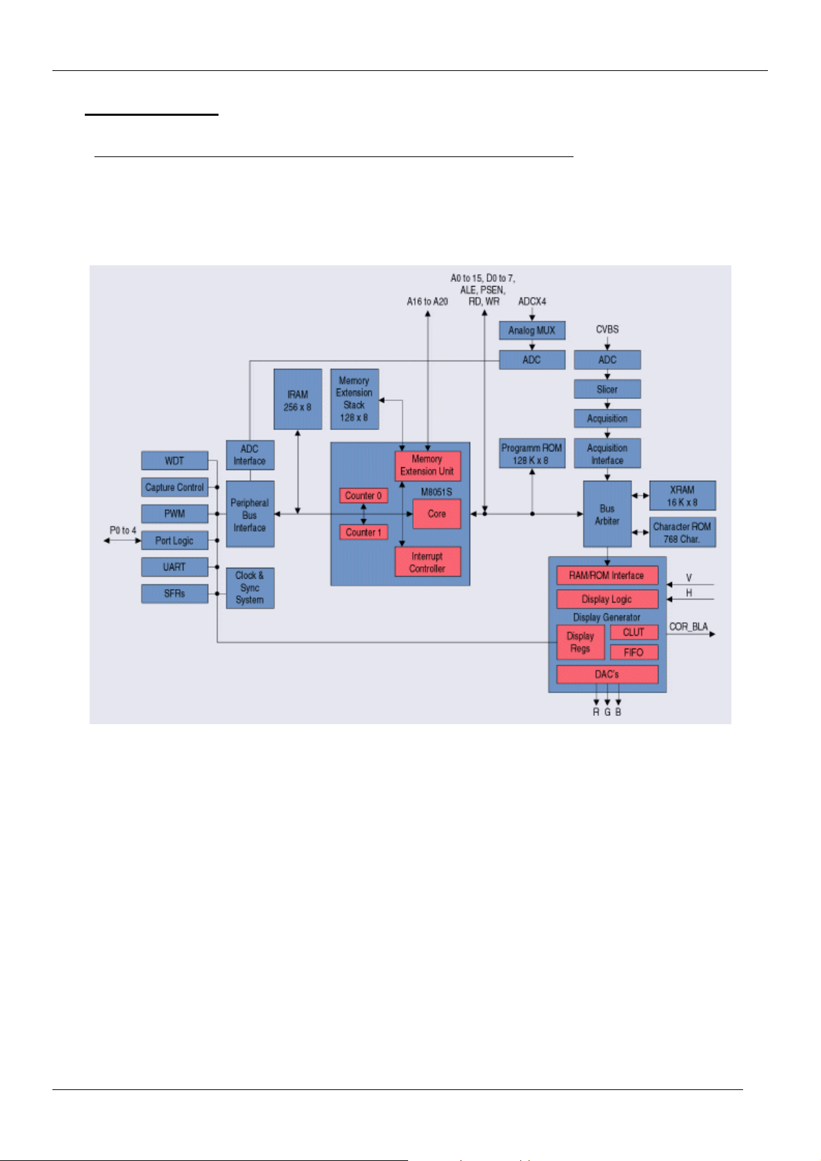
4 IC DESCRIPTION.................................................................................................................18
4.1 TELETEXT DECODER WITH EMBEDDED 8-BIT CONTROLLER...................................18
4.1.1 BLOCK DIAGRAM OF THE SDA55XX........................................................................18
4.1.2 DESCRIPTION ............................................................................................................18
4.1.3 IC MARKING AND VERSION......................................................................................19
4.1.4 PINNING......................................................................................................................19
4.2 VSP94X5B (VERSION C4)– OPTIMUS COLOR DECODER AND SCAN-RATE
CONVERTER....................................................................................................................21
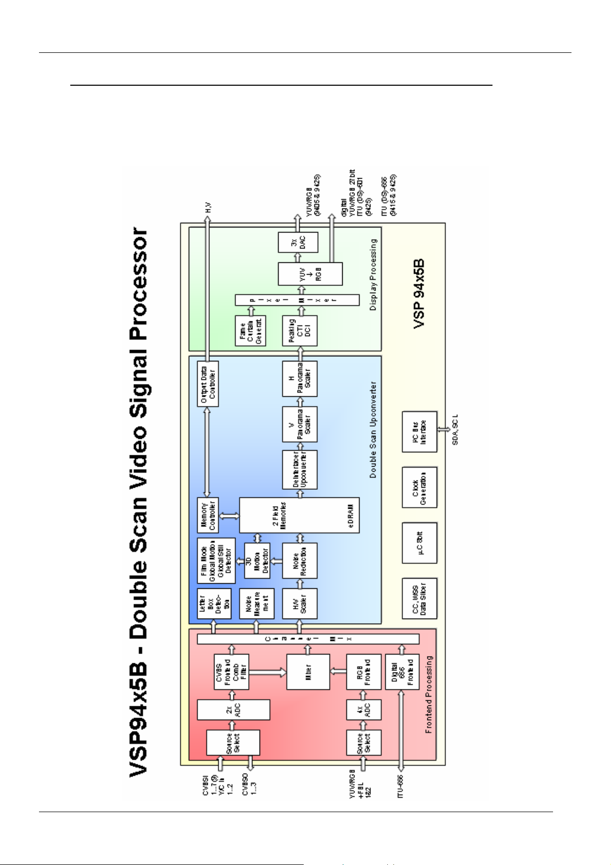
4.2.1 BLOCK DIAGRAM OF THE VSP94x5B ......................................................................21
4.2.2 Feature Overview ........................................................................................................22
4.2.3 PINNING......................................................................................................................23
4.3 DDP 3315C – DISPLAY AND DEFLECTION PROCESSOR............................................25
4.3.1 BLOCK DIAGRAM OF THE DDP 3315C.....................................................................25
4.3.2 DESCRIPTION ............................................................................................................25
4.3.3 PINNING......................................................................................................................27
4.4 MSP341X MULTISTANDARD SOUND PROCESSOR.....................................................29
4.4.1 BASIC FEATURES OF THE MSP 341X......................................................................29
4.4.1.1 Demodulator & NICAM Decoder Section..................................................................29
4.4.1.2 DSP-Section (Audio Baseband Processing) .............................................................30
4.4.1.3 Analogue Section......................................................................................................30
4.4.1.4 NICAM & FM/AM-Mono ............................................................................................30
Europe R&D
1

CP-850FX Service Manual
4.4.1.5 German 2-Carrier System (DUAL FM System).........................................................30
4.5 TDA4470 - MULTISTANDARD VIDEO-IF AND QUASI PARALLEL SOUND PROCESSOR .......33
4.5.1 DESCRIPTION ............................................................................................................33
4.5.2 FEATURES..................................................................................................................33
4.5.3 PINNING......................................................................................................................33
4.5.4 BLOCK DIAGRAM.......................................................................................................34
4.6 TDA8946J STEREO AUDIO AMPLIFIER .........................................................................35
4.6.1 FEATURES..................................................................................................................35
4.7 TDA8358J VERTICAL AMPLIFIER...................................................................................37
4.7.1 FEATURES..................................................................................................................37
4.8 TDA6108JF.......................................................................................................................39
4.9 24C16 - 16 KB EEPROM ..................................................................................................40
4.10 STR – W6754....................................................................................................................41
4.10.1 GENERAL DESCRIPTION ........................................................................................41
4.10.2 FEATURES................................................................................................................41
4.10.3 BLOCK DIAGRAM.....................................................................................................41
4.10.4 PIN DESCRIPTION ...................................................................................................42
4.10.5 MOSFET ELECTRICAL CHARACTERISTICS ..........................................................42
4.10.6 ELECTRICAL CHARACTERISTICS..........................................................................43
5 CP-850FX CHASSIS DESCRIPTION...................................................................................44
5.1 POWER SUPPLY BLOCK DIAGRAM...............................................................................44
5.2 VIDEO & STEREO AUDIO BLOCK DIAGRAM.................................................................45
5.3 IF SECTION......................................................................................................................46
5.3.1 BLOCK DIAGRAM.......................................................................................................46
5.3.2 VISION IF AMPLIFIER ................................................................................................47
5.3.3 TUNER-AND VIF-AGC ................................................................................................47
5.3.4 FPLL, VCO AND AFC..................................................................................................47
5.3.5 VIDEO DEMODULATION AND AMPLIFIER ...............................................................48
5.3.6 SOUND IF AMPLIFIER AND SIF-AGC........................................................................48
5.3.7 QUASI-PARALLEL-SOUND (QPS) MIXER .................................................................48
5.3.8 STANDARD SWITCH..................................................................................................48
5.3.9 L’ SWITCH...................................................................................................................48
5.3.10 INTERNAL VOLTAGE STABILISER .........................................................................48
5.4 VIDEO / RGB ....................................................................................................................48
5.4.1 FRONT END................................................................................................................48
5.4.1.1 CVBS Front-End .......................................................................................................48
5.4.1.2 Input Selector............................................................................................................49
5.4.1.3 Signal Levels And Gain Control ................................................................................49
5.4.1.4 Synchronization ........................................................................................................49
5.4.1.5 Chroma Decoder ......................................................................................................49
5.4.1.6 Luminance Processing..............................................................................................49
5.4.1.7 RGB Front-End .........................................................................................................49
5.4.1.8 Signal Processing .....................................................................................................49
5.3.1.8.1 Horizontal Prescaler...............................................................................................49
5.3.1.8.2 Noise Reduction .....................................................................................................50
5.3.1.8.3 Noise Measurement............................................................................................... 50
5.3.1.8.4 Operation Modes ...................................................................................................50
5.3.1.8.5 Digital 656 Output ..................................................................................................50
5.4.2 BACK END ..................................................................................................................50
5.4.2.1 Digital Input Interface................................................................................................50
5.4.2.2 Horizontal Scaler ......................................................................................................50
5.4.2.3 Luma Contrast and Brightness .................................................................................51
Europe R&D
2

CP-850FX Service Manual
5.4.2.4 Black Level Expander/Compressor (BLEC) .............................................................. 51
5.4.2.5 Luma Sharpness Enhancer (LSE) ............................................................................51
5.4.2.6 Dynamic Peaking......................................................................................................51
5.4.2.7 Luma Transient Improvement (LTI) ..........................................................................51
5.4.2.8 Mixing of Dynamic Peaking and LTI .........................................................................51
5.4.2.9 Chroma Transient Improvement ...............................................................................51
5.4.2.10 Analog Back End ....................................................................................................53
5.4.2.11 Analog RGB Insertion .............................................................................................53
5.4.2.12 CRT Measurement and Control ..............................................................................53
5.4.2.13 Synchronization and Deflection ..............................................................................54
5.4.2.14 EHT Compensation ................................................................................................54
5.5 MICRONTROLLER ...........................................................................................................54
5.5.1 MICROCONTROLLER FEATURES ............................................................................54
5.5.2 ACQUISITION FEATURES .........................................................................................54
5.5.3 PORTS ........................................................................................................................55
5.5.4 μ-CONTROLLER I/O PIN CONFIGURATION AND FUNCTION TABLE .....................55
5.5.5 TUNING.......................................................................................................................55
5.5.6 AUTOMATIC PICTURE FORMAT SWITCHING .........................................................56
5.5.6.1 WSS Data .................................................................................................................56
5.5.6.2 SCART Pin 8 Data (Slow Switching) ........................................................................57
5.5.6.3 Picture Format Description .......................................................................................57
5.3.1.8.1 16:9 CRT ...............................................................................................................57
5.3.1.8.2 4:3 CRT .................................................................................................................58
5.5.7 EXTERNAL SOURCE CONTROL LOGIC...................................................................59
5.5.8 OVER CURRENT PROTECTION................................................................................60
5.6 TELETEXT DISPLAY........................................................................................................60
5.7 SOUND PROCESSING ....................................................................................................61
5.7.1 ANALOGUE SOUND IF - INPUT SECTION...............................................................61
5.7.2 QUADRATURE MIXERS.............................................................................................61
5.7.3 PHASE AND AM DISCRIMINATION ...........................................................................61
5.7.4 NICAM DECODER ......................................................................................................62
5.7.5 DSP SECTION ............................................................................................................62
5.7.6 SOUND MODE SWITCHING.......................................................................................62
5.8 SOUND AMPLIFICATION................................................................................................. 62
5.8.1 POWER AMPLIFIER ...................................................................................................62
5.8.2 MODE SELECTION.....................................................................................................63
5.9 VERTICAL DEFLECTION.................................................................................................63
5.9.1 FLYBACK VOLTAGE ..................................................................................................63
5.9.2 PROTECTION .............................................................................................................63
5.9.3 GUARD CIRCUIT ........................................................................................................63
5.9.4
DAMPING RESISTOR.................................................................................................63
5.9.5 EAST-WEST AMPLIFIER............................................................................................63
5.10 POWER SUPPLY (STR-W6754) - FUNCTIONS OF EACH TERMINAL ..........................64
5.10.1 Vcc Terminal (Pin 4)...................................................................................................64
5.10.1.1 Start-up Circuit........................................................................................................64
5.10.1.2 Auxiliary/Drive Winding...........................................................................................65
5.10.1.3 Overvoltage Protection Circuit ................................................................................66
5.10.1.4 Latch Circuit............................................................................................................67
5.10.2 SS/OLP Terminal (Pin 5)..........................................................................................67
5.10.2.1
5.10.2.2
5. 10. 2. 3
Soft-Start Operation at Start-up of Power Supply ...................................................67
Overload Protection ................................................................................................68
Operation at Power Supply OFF ...........................................................................69
Europe R&D
3

CP-850FX Service Manual
5.10.2.4 Cancellation of OLP Circuit.......................................................................................69
5.10.3 FB Terminal (Pin. 6)...................................................................................................70
5.10.3.1 Constant Voltage Control Circuit............................................................................. 70
5.10.4 OCP/BD Terminal (Pin 7)...........................................................................................71
8.4.1. Minus-Detection Type OCP Circuit .............................................................................71
5.10.5 Quasi-Resonant and Bottom-Skip Operation.............................................................72
5.10. 5. 1 Quasi-Resonant Operation.....................................................................................72
5.10.5.2 Bottom-Skip Operation (Switching from Quasi-Resonant Operation) .....................73
1). Quasi-Resonant Operation ⇒ Bottom-Skip Operation.............................................73
2). Bottom-Skip Operation ⇒ Quasi-Resonant Operation ...............................................73
5.10.6 Stand-By Operation ...................................................................................................74
5.10.7 Step-Drive Circuit.......................................................................................................76
5.10.8 Maximum ON Time Controlling Function ...................................................................76
6 SERVICE PARTS LIST ........................................................................................................77
6.1 DTF-2950..........................................................................................................................77
7 EXPLODED VIEW................................................................................................................85
7.1 DTF-2950..........................................................................................................................85
8 PRINTED CIRCUIT BOARD.................................................................................................86
8.1 MAIN PCB.........................................................................................................................86
8.2 UNION PCB .............................................................................................................................87
8.3 CRT PCB ..........................................................................................................................88
9 SCHEMATIC DIAGRAM.......................................................................................................89
9.1 MAIN.................................................................................................................................89
9.2 UNION & CRT...................................................................................................................90
Europe R&D
4

CP-850FX Service Manual
DOCUMENT HISTORY
VERSION DATE COMMENTS
V1.00 31/07/06 Creation of document (Author JS KIM) for project CP-850FX 100Hz TV.
Europe R&D
5
1 MAIN FEATURES
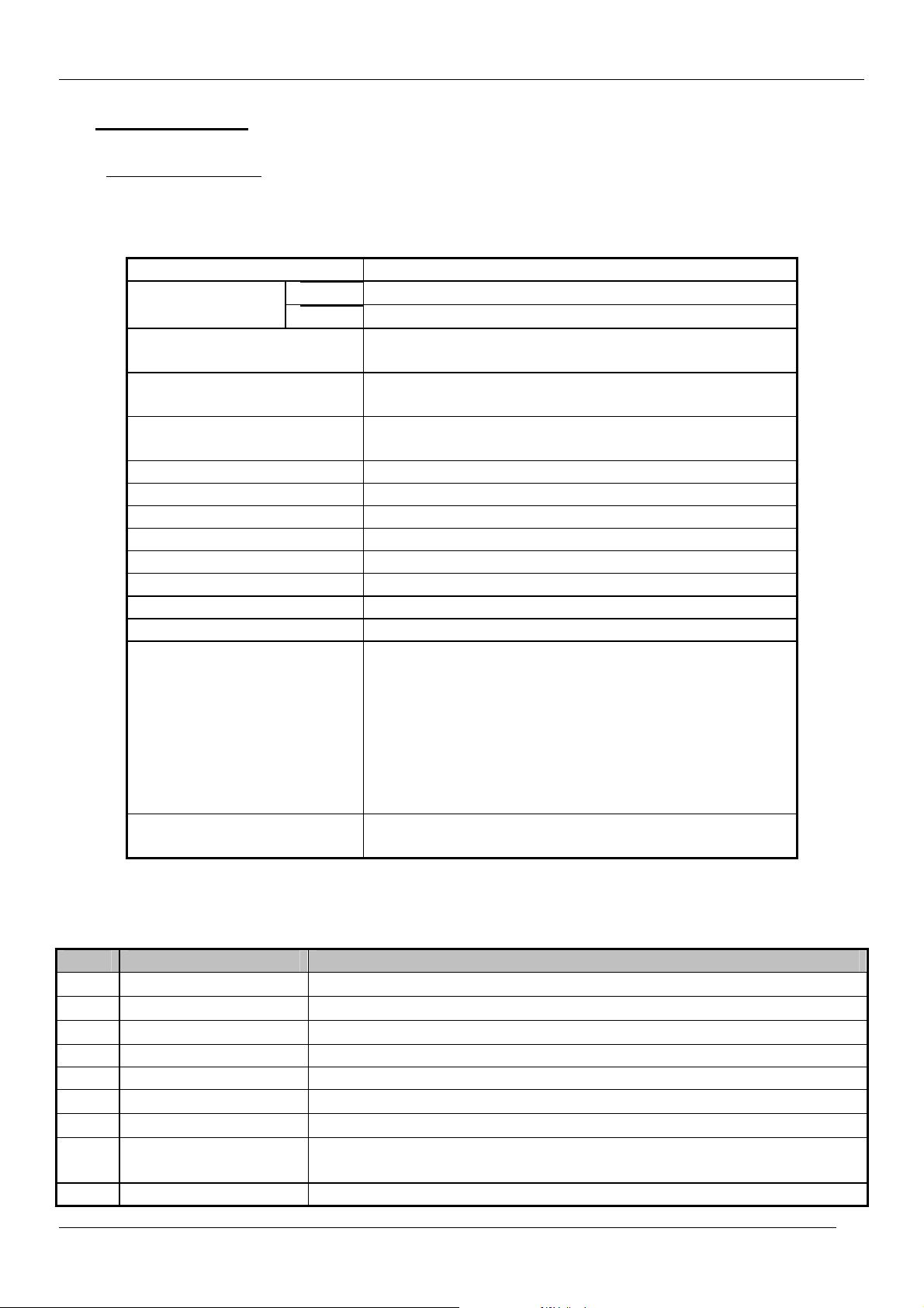
1.1 SPECIFICATIONS
1.1.1 GENERAL
TV standard PAL/SECAM-B/G, D/K, PAL-I/I, SECAM-L/L’
Sound system NICAM B/G, I, D/K, L,
Power
consumption
Sound Output
Power
Speaker 12W 8 ohm x2
Teletext system 9 pages memory FASTEXT (FLOF or TOP)
Aerial input 75 ohm unbalanced
Channel coverage Off-air channels, S-cable channels and hyperband
Tuning system frequency synthesiser tuning system
Visual screen size 68cm
Channel indication On Screen Display
Program Selection 100 programmes
Aux. terminal EURO-SCART 1 : Audio / Video In and Out, R/G/B
Remote Control
Unit
CP-850FX Service Manual
Tuner PAL, SECAM Colour system
AV PAL, SECAM, PAL 60, NTSC M, NTSC 4.43
FM 2Carrier B/G, D/K
105W
7W x 2 (at 60% mod, 10%THD)
In, Slow and Fast switching.
EURO-SCART 2 : Audio / Video In and Out, SVHS
In.
AV3 : Audio-Video Jack on side of cabinet.
Headphone jack (3.5 mm) on side of cabinet
SVHS3 : Jack on side of cabinet – sound input
common with AV3.
R-49C10(AAA)
1.1.2 EURO-SCART 1 (21 Pin)
Pin Signal Description Matching value
1 Audio Output Right
2 Audio Input Right
3 Audio Output Left
4 Audio Earth
5 Blue Earth
6 Audio Input Left
7 Blue Input
8 Slow Switching TV : 0 to 2V, AV 16/9 : 4.5 to 7V, AV 4/3 : 9.5 to 12V , Impedance
9 Green Earth
Europe R&D
0.5 Vrms, Impedance < 1 kΩ, ( RF 54% Mod )
0.5 Vrms, Impedance > 10 kΩ
0.5 Vrms, Impedance < 1 kΩ, ( RF 54% Mod )
0.5 Vrms, Impedance > 10 kΩ
0.7 Vpp ±0.1V, Impedance 75Ω
> 10 kΩ
6
CP-850FX Service Manual
10 N.C.
11 Green Input
12 N.C.
13 Red Earth
14 Blanking Earth
15 Red Input
16 Fast Switching
17 Video Out Earth
18 Video In Earth
19 Video Output
20 Video Input
21 Common Earth
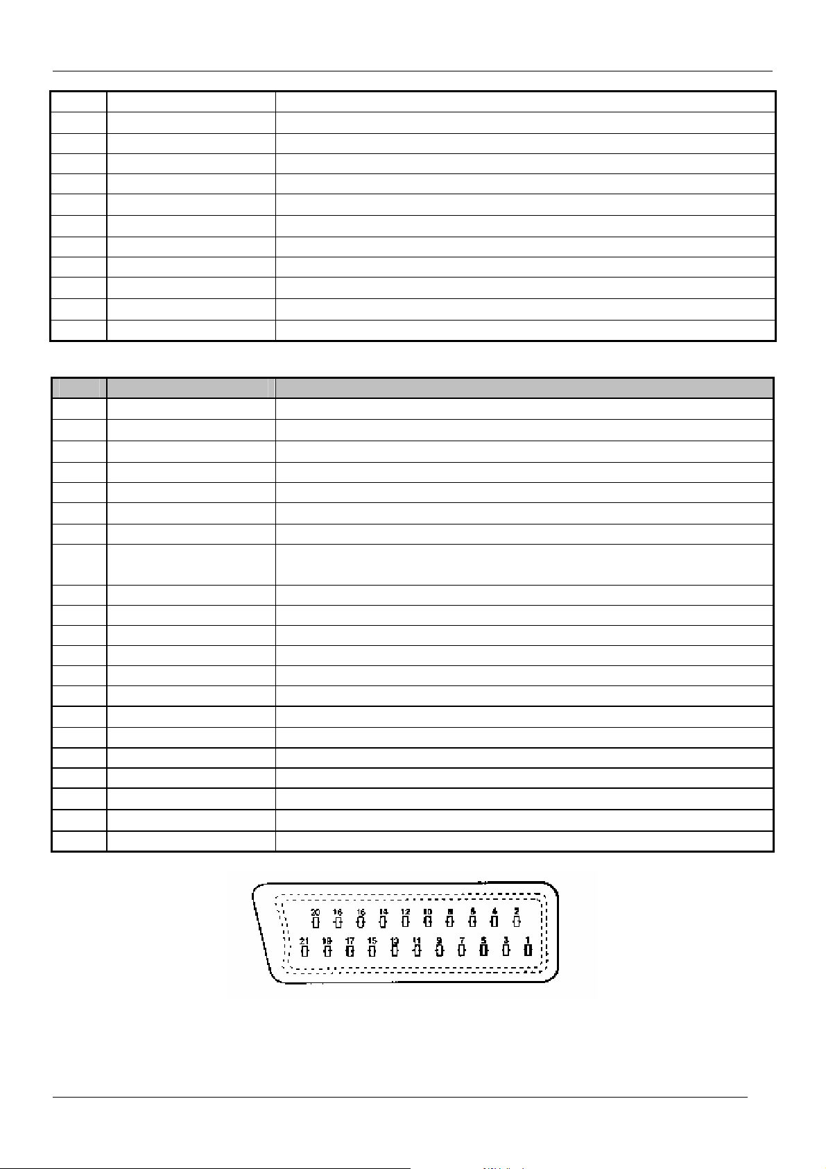
1.1.3 EURO-SCART 2 (21 Pin)
Pin Signal Description Matching value
1 Audio Output Right
2 Audio Input Right
3 Audio Output Left
4 Audio Earth
5 Earth
6 Audio Input Left
7 N.C.
8 Slow Switching TV : 0 to 2V, AV 16/9 : 4.5 to 7V, AV 4/3 : 9.5 to 12V , Impedance
9 Earth
10 N.C.
11 N.C.
12 N.C.
13 Earth
14 Earth
15 Chroma Input
16 N.C.
17 Earth
18 Video In Earth
19 Video Output
20 Video Input, Y In.
21 Common Earth
0.7 Vpp ± 0.1V, Impedance 75Ω
0.7 Vpp ± 0.1V, Impedance 75Ω
0 to 0.4V : Logic “0”, 1 to 3V : Logic “1”, Impedance 75Ω
1 Vpp ± 3dB, Impedance 75Ω
1 Vpp ± 3dB, Impedance 75Ω
0.5 Vrms, Impedance < 1 kΩ, ( RF 54% Mod )
0.5 Vrms, Impedance > 10 kΩ
0.5 Vrms, Impedance < 1 kΩ, ( RF 54% Mod )
0.5 Vrms, Impedance > 10 kΩ
> 10 kΩ
± 3dB for a luminance signal of 1 Vpp
1 Vpp ± 3dB, Impedance 75Ω ( Monitor output )
1 Vpp ± 3dB, Impedance 75Ω
Europe R&D
7

CP-850FX Service Manual
1.2 CHANNEL/FREQUENCY TABLE
CHANNEL EUROPE CCIR FRANCE GB(IRELAND) EAST OIRT
C01
C02
C03
C04
C05
C06
C07
C08
C09
C10
C11
C12
C13
C14
C15
C16
C17
C18
C19
C20
C21
C22
C23
C24
C25
C26
C27
C28
C29
C30
C31
C32
C33
C34
C35
C36
C37
C38
C39
C40
C41
C42
C43
C44
C45
C46
46.25 - 45.75 49.75
48.25 55.75 (L') 53.75 59.25
55.25 60.5 (L') 61.75 77.25
62.25 63.75 (L') 175.25 85.25
175.25 176.00 183.25 93.25
182.25 184.00 191.25 175.25
189.25 192.00 199.25 183.25
196.25 200.00 207.25 191.25
203.25 208.00 215.25 199.25
210.25 216.00 223.25 207.25
217.25 189.25 (LUX) 231.25 215.25
224.25 69.25 (L') 239.25 223.25
53.75 76.25 (L') 247.25 -
- 83.25 (L') 49.75 -
82.25 90.25 57.75 -
- 97.25 65.75 -
183.75 - 77.75 -
192.25 - 85.75 -
201.25 - - -
- - - -
471.25 471.25 471.25 471.25
479.25 479.25 479.25 479.25
487.25 487.25 487.25 487.25
495.25 495.25 495.25 495.25
503.25 503.25 503.25 503.25
511.25 511.25 511.25 511.25
519.25 519.25 519.25 519.25
527.25 527.25 527.25 527.25
535.25 535.25 535.25 535.25
543.25 543.25 543.25 543.25
551.25 551.25 551.25 551.25
559.25 559.25 559.25 559.25
567.25 567.25 567.25 567.25
575.25 575.25 575.25 575.25
583.25 583.25 583.25 583.25
591.25 591.25 591.25 591.25
599.25 599.25 599.25 599.25
607.25 607.25 607.25 607.25
615.25 615.25 615.25 615.25
623.25 623.25 623.25 623.25
631.25 631.25 631.25 631.25
639.25 639.25 639.25 639.25
647.25 647.25 647.25 647.25
655.25 655.25 655.25 655.25
663.25 663.25 663.25 663.25
671.25 671.25 671.25 671.25
Europe R&D
8

CP-850FX Service Manual
C47
C48
C49
C50
C51
C52
C53
C54
C55
C56
C57
C58
C59
C60
C61
C62
C63
C64
C65
C66
C67
C68
C69
C70
C71
C72
C73
C74
C75
C76
C77
S01
S02
S03
S04
S05
S06
S07
S08
S09
S10
S11
S12
S13
S14
S15
S16
S17
S18
679.25 679.25 679.25 679.25
687.25 687.25 687.25 687.25
695.25 695.25 695.25 695.25
703.25 703.25 703.25 703.25
711.25 711.25 711.25 711.25
719.25 719.25 719.25 719.25
727.25 727.25 727.25 727.25
735.25 735.25 735.25 735.25
743.25 743.25 743.25 743.25
751.25 751.25 751.25 751.25
759.25 759.25 759.25 759.25
767.25 767.25 767.25 767.25
775.25 775.25 775.25 775.25
783.25 783.25 783.25 783.25
791.25 791.25 791.25 791.25
799.25 799.25 799.25 799.25
807.25 807.25 807.25 807.25
815.25 815.25 815.25 815.25
823.25 823.25 823.25 823.25
831.25 831.25 831.25 831.25
839.25 839.25 839.25 839.25
847.25 847.25 847.25 847.25
855.25 855.25 855.25 855.25
863.25 863.25 863.25 863.25
69.25 - - -
76.25 - - -
83.25 - - -
90.25 - - -
97.25 - - -
59.25 - - -
93.25 - - -
105.25 104.75 103.25 105.25
112.25 116.75 111.25 112.25
119.25 128.75 119.25 119.25
126.25 140.75 127.25 126.25
133.25 152.75 135.25 133.25
140.25 164.75 143.25 140.25
147.25 176.75 151.25 147.25
154.25 188.75 159.25 154.25
161.25 200.75 167.25 161.25
168.25 212.75 - 168.25
231.25 224.75 - 231.25
238.25 236.75 - 238.25
245.25 248.75 255.25 245.25
252.25 260.75 263.25 252.25
259.25 272.75 271.25 259.25
266.25 284.75 279.25 266.25
273.25 296.75 287.25 273.25
280.25 136.00 295.25 280.25
Europe R&D
9

CP-850FX Service Manual
S19
S20
S21
S22
S23
S24
S25
S26
S27
S28
S29
S30
S31
S32
S33
S34
S35
S36
S37
S38
S39
S40
S41
287.25 160.00 303.25 287.25
294.25 - - 294.25
303.25 303.25 - 303.25
311.25 311.25 311.25 311.25
319.25 319.25 319.25 319.25
327.25 327.25 327.25 327.25
335.25 335.25 335.25 335.25
343.25 343.25 343.25 343.25
351.25 351.25 351.25 351.25
359.25 359.25 359.25 359.25
367.25 367.25 367.25 367.25
375.25 375.25 375.25 375.25
383.25 383.25 383.25 383.25
391.25 391.25 391.25 391.25
399.25 399.25 399.25 399.25
407.25 407.25 407.25 407.25
415.25 415.25 415.25 415.25
423.25 423.25 423.25 423.25
431.25 431.25 431.25 431.25
439.25 439.25 439.25 439.25
447.25 447.25 447.25 447.25
455.25 455.25 455.25 455.25
463.25 463.25 463.25 463.25
Europe R&D
10
CP-850FX Service Manual
1.3 ATSS SORTING METHOD
The TV set sweeps all the TV bands from beginning of VHF to end of UHF. The TV controlling
software for each program checks if a VPS CNI code is transmitted (this system exists for
German, Swiss and Austrian transmissions).
If no VPS CNI code is found, then the system checks if a CNI code is transmitted as part of the
teletext transmission ( Packet 8/30 format 1 and format 2). If such a code ( VPS or teletext ) is
found and if this code is in the ATSS list, the program is automatically named.
If the transmission does not have VPS CNI, and no teletext service is available, then there is no
possibility of the program being automatically named.
The programs found are then sorted in 4 groups :
Group I : It contains all the programs from the selected country and named by the TV controlling
software. Within this group the sorting order is fixed by the ATSS list.
Group II : It contains all the programs with a strong signal strength which are not listed in group I.
Group III : It contains all the programs with a weak signal strength which are not listed in group I.
Group IV : If two or more programs with the same code are found, only the strongest ( or if they
have the same level the one with the lowest frequency) is listed in group I, II or III. The others are
listed in group IV.
1.3.1 GENERAL CASE
Program
number
1
2 Group I
...
n
n+1
... Group II
m
m+1
... Group III
p
p+1
... Group IV
q
q+1
... not used
99
0
Group Skip
9
9
1.3.2 SPECIAL CASE
Program
number
1
... Group II
m
m+1
... Group III
p
p+1
... Group IV
q
q+1
... not used
99
0
Special case : Country selection = Others
Group Skip
9
9
Europe R&D
11

CP-850FX Service Manual
Note : If two programs with the same name but a different code are found these two programs
are listed in group I, II or III .
The sorting order within group II, III, and IV is based on the channel frequency. The program with
the lowest frequency is allocated the first rank in its group, and so forth until the last program of
the group which has the highest frequency.
Special case : France
If France is selected, the TV controlling software first sweeps all TV bands with France system
selected ( positive video modulation) and then a second time with Europe system selected
( negative video modulation).
Special case : Switzerland
If Switzerland is selected the TV controlling software first sweeps all TV bands with Europe
system selected (negative video modulation) and then a second time with France system
selected ( positive video modulation).
Special case : GB
Note for satellite receiver users : Before starting ATSS turn on your satellite receiver and tune to
“ SKY NEWS “.
If GB is selected the TV controlling software seeks for programs only in UHF ( C21 to C70 ). The
sorting order is :
1 - BBC1
2 - BBC2
3 - ITV
4 - CH4
5 - CH5
6 – NEWS (Sky News)
If two or more “ identical “programs ( same name but different code e.g. BBC1 and BBC1
Scotland ) are found the following programs in the list will be shifted up. (1 - BBC1, 2 - BBC1, 3 BBC2, 4 - ITV, 5 - CH4, 6 - CH5, 7 - NEWS, ..)
If one of the programs above is not found, the associated program number remains empty
( freq.=467.25 MHz - Skip selected - no name – system = GB).
example A : 1 - BBC1, 2 - BBC2, 3 - ITV, 4 - -----, 5 - CH5, 6 - NEWS, ...
example B ( if 2 BBC1 found ) : 1 - BBC1, 2 - BBC1, 3 - BBC2, 4 - ITV, 5 - -----, 6 - CH5, 7 NEWS, ...
Europe R&D
12

CP-850FX Service Manual
2 SAFETY INSTRUCTION
WARNING: Only competent service personnel may carry out work involving the testing or repair
of this equipment.
X-RAY RADIATION PRECAUTION
1. Excessive high voltage can produce potentially hazardous X-RAY RADIATION. To avoid
such hazards, the high voltage must not exceed the specified limit. The nominal value of the high
voltage of this receiver is 25-26 KV (20”-21”) or 26 KV (25” - 28”) at max beam current. The high
voltage must not, under any circumstances, exceed 27.5 KV (20”), 29KV (21”), 29.5 KV (25") or
30 KV (28"). Each time a receiver requires servicing, the high voltage should be checked. It is
important to use an accurate and reliable high voltage meter.
2. The only source of X-RAY Radiation in this TV receiver is the picture tube. For continued
X-RAY RADIATION protection, the replacement tube must be exactly the same type tube as
specified in the parts list.
SAFETY PRECAUTION
Potentials of high voltage are present when this receiver is operating. Operation of the receiver
outside the cabinet or with the back board removed involves a shock hazard from the receiver.
Servicing should not be attempted by anyone who is not thoroughly familiar with the precautions
necessary when working on high voltage equipment.
Discharge the high potential of the picture tube before handling the tube. The picture tube is
highly evacuated and if broken, glass fragments will be violently expelled.
If any Fuse in this TV receiver is blown, replace it with the FUSE specified in the Replacement
Parts List.
When replacing a high wattage resistor (metal oxide film resistor) in the circuit board, keep the
resistor 10 mm away from circuit board.
Keep wires away from high voltage or high temperature components.
This receiver must operate under AC 230 volts, 5O Hz. NEVER connect to a DC supply or any
other voltage or frequency.
PRODUCT SAFETY NOTICE
Many electrical and mechanical parts in this equipment have special safety-related
characteristics. These characteristics are often passed unnoticed by a visual inspection and the
X-RAY RADIATION protection afforded by them cannot necessarily be obtained by using
replacement components rated for higher voltage, wattage, etc. Replacement parts which have
these special safety characteristics are identified in this manual and its supplements, electrical
components having such features are identified by designated symbol on the parts list. Before
replacing any of these components, read the parts list in this manual carefully. The use of
substitutes replacement parts which do not have the same safety characteristics as specified in
the parts list may create X-RAY Radiation.
Europe R&D
13

CP-850FX Service Manual
3 ALIGNMENT INSTRUCTIONS
3.1 MICROCONTROLLER CONFIGURATION : SERVICE MODE
To switch the TV set into service mode please see instruction below.
1 - Select PR. number 91
2 - Adjust sharpness to minimum and exit all menus.
3 – Within 2 seconds press the key sequence : RED - GREEN - menu
The software version is displayed beside the word Service, e.g. “SERVICE V1.00”.
To exit SERVICE menu press menu key or Std By key.
3.2 SERVICE MODE NAVIGATION
Pr Up/Down remote keys : cycle through the service items available.
Vol -/+ remote keys : Dec./Increment the values within range – Cycle trough option bits.
OK key : Toggle bits in option byte
Order Item Default setting
Note:All settings are approximate
1 HOR CEN -154
2 RED GAIN 412
3 GRN GAIN 363
4 BLUE GAIN 380
5 RED BIAS 226
6 GRN BIAS 210
7 AGC LEVEL 56
8 G2 – SCREEN 32
9 AFT 32
10 AVL OFF
11 OPTION1 0011 1000 [0x38]
12 OPTION2 0000 0110 [0x06]
13 OPTION3 1111 1111 [0xFF]
14 PARABOLA 346
15 HOR WIDTH -71
16 CORNER T -100
17 CORNER B -30
18 HOR. PARAL 2
19 V. LINEAR 16
20 EW TRAPEZ 12
21 S CORRECT 130
22 VERT CENT -14
23 VERT SIZE 40
24 SHIPPING OFF
3.3 MICROCONTROLLER CONFIGURATION : OPTION BITS
There are three option bytes available (16 bits in all). These option bits are available from
Service mode. First find the OPTION1 or OPTION2 control, and then use the Volume
PLUS/MINUS buttons on the remote control keypad to locate the bits, and OK key to toggle them.
The table below shows the two option bytes available;
Europe R&D
14
CP-850FX Service Manual
3.3.1 OPTION 1
B7 B6 B5 B4 B3 B2 B1 B0
TOP
1
Teletext
OFF
TOP
0
Teletext
ON
3.3.2 OPTION 2
1
0
3.3.3 OPTION 3
B7 B6 B5 B4 B3 B2 B1 B0
1
0
1.00 1.15 0 0 1
1.05 1.20 0 1 0
1.10 1.25 0 1 1
LG PHILIPS CRT 1.25 1.40 1 0 1
SAMSUNG SDI CRT 1.30 1.45 1 1 0
1.35 1.50 1 1 1
All values modified are immediately memorised in eeprom.
B7 B6 B5 B4 B3 B2 B1 B0
Fixed to
‘0’
Must be set to “1” for future
FASTEXT
(FLOF)
OFF
FASTEXT
(FLOF)
ON
JVC
remote
control
Daewoo
Remote
control
compatibility
Tube
TUBE
4:3
TUBE
16:9
AVL
control
OFF
AVL
control
ON
Headphone
Volume/Bal
ance control
OFF
Headphone
Volume/Bal
ance control
ON
PICTURE
TILT ON
PICTURE
TILT OFF
Local
keyboard : 6
keys
Local
keyboard : 5
keys
Beam
Nominal Max
0.95 1.10 0 0 0
1.20 1.35 1 0 0
Dolby
Virtual
OFF
Dolby
Virtual
ON
Program
list
enabled
Program
list
disabled
Must be
set to “1”
for future
compatibi
lity ( See
CP830
NEC)
Current
(mA)
SVHS3
disable
SVHS3
enable
See table below
OSD
display
“AV” in
extern
mode
OSD
display
“EXT” in
extern
mode
(JVC
only)
B2 B1 B0
Tuner options
00 = Philips
01 = not used
10 = ALPS
11 = PARTSNIC
AV3
Enabled
AV3
Disable
d
(NEC
only)
Full
ATSS
Basic
ATSS
Europe R&D
15
CP-850FX Service Manual
3.4 TV SET ALIGNMENT
3.4.1 LOCAL OSCILLATOR ALIGNMENT
Tune a colour bar pattern. The frequency of the signal carrier must be accurate ( Max +/- 10KHz
deviation from the nominal channel frequency).
Find “AFT” item in service mode.
Adjust the coil L150 to bring the cursor to central position : 32.
3.4.2 G2 ALIGNMENT
- Tune a colour bar pattern.
- Find the “G2 – SCREEN” item in service mode.
- Adjust screen volume ( on FBT ) to bring the cursor to central position : 32.
3.4.3 WHITE BALANCE
- Select a dark picture and adjust RED BIAS and GRN BIAS to the desired colour temperature.
- Select a bright picture and adjust RED, GRN and BLUE GAIN to the desired colour temperature.
3.4.4 FOCUS
Adjust the Focus volume ( on FBT ) to have the best resolution on screen.
3.4.5 VERTICAL GEOMETRY
Adjust V. LINEAR (linearity), S CORRECT (S. Correction), VERT SIZE (Vertical amplitude),
VERT CENT (vertical centring) to compensate for vertical distortion.
3.4.6 HORIZONTAL PICTURE CENTRING
Adjust HOR CEN (Horizontal centre) to have the picture in the centre of the screen.
3.4.7 EAST / WEST CORRECTION
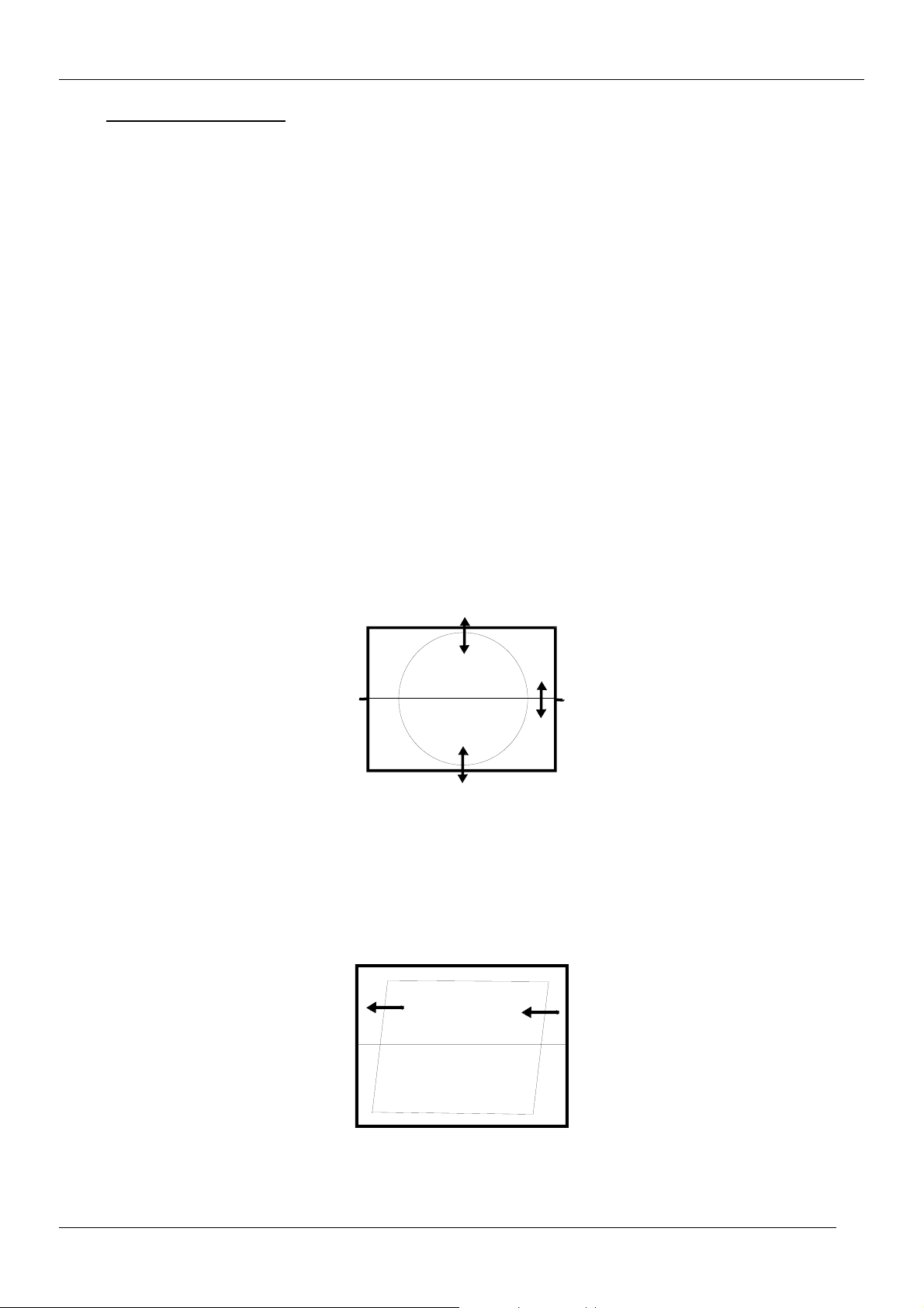
Adjust the PARABOLA, HOR WIDTH, CORNER, HOR PARAL, EW TRAPEZ, to compensate for
geometrical distortion.
Europe R&D
HOR PARAL
16
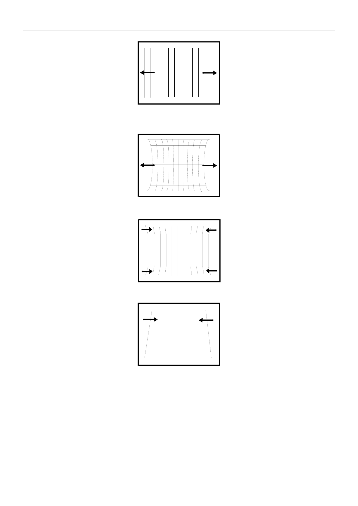
CP-850FX Service Manual
HOR WIDTH
adjust for 93% overscan.
PARABOLA
CORNER B & CORNER T
EW TRAPEZ
3.4.8 AGC
- Make sure option bits are correct for the tuner fitted on the chassis (See above how to change
option bits).
- Adjust the antenna signal level at 62 dBμV± 1
- Tune a colour bar pattern.
- Find the “AGC” item in service mode.
- Press the key “OK” on the remote keypad and wait until AGC level stabilise to the optimum
value.
- Alternatively, use “Vol Up/Dwn” keys to adjust manually to the desired Tuner Take Over Point
(TOP).
Europe R&D
17
CP-850FX Service Manual
4 IC DESCRIPTION
4.1 TELETEXT DECODER WITH EMBEDDED 8-BIT CONTROLLER
TVText Pro is a 8-bit controller based on a enhanced 8051 core with embedded teletext, On
screen Display and TV controller functions.
4.1.1 BLOCK DIAGRAM OF THE SDA55XX
4.1.2 DESCRIPTION
The SDA 55xx is a single chip teletext decoder for decoding World System Teletext data as well
as Video Programming System (VPS), Program Delivery Control (PDC), and Wide Screen
Signalling (WSS) data used for PAL plus transmissions (line 23).
The device provides an integrated general-purpose, fully 8051-compatible Microcontroller with
television specific hardware features. The microcontroller has been enhanced to provide
powerful features such as memory banking, data pointers and additional interrupts etc.
The on-chip display unit for displaying Level 1.5 teletext data is also used for customer defined
on-screen displays. Internal XRAM consists of 16 Kbytes. Device has an internal ROM of 128
Kbytes.
The SDA 55xx supports a wide range of standards including PAL, NTSC and contains a digital
slicer for VPS, WSS, PDC, TTX and Closed Caption, an accelerating acquisition hardware
module, a display generator for Level 1.5 TTX data and powerful On screen Display capabilities
based on parallel attributes, and Pixel oriented characters (DRCS).
The 8-bit Microcontroller runs at 360 ns. cycle time (min.). Controller with dedicated hardware
does most of the internal TTX acquisition processing, transfers data to/from external memory
Europe R&D
18
CP-850FX Service Manual
interface and receives/transmits data via I 2 C-firmware user-interface. The slicer combined with
dedicated hardware stores TTX data in a VBI buffer of 1 Kilobyte. The Microcontroller firmware
performs all the acquisition tasks (hamming-and parity-checks, page search and evaluation of
header control bits) once per field. Additionally, the firmware can provide high-end Teletextfeatures like Packet-26-handling, FLOF, TOP and list-pages.
4.1.3 IC MARKING AND VERSION
Chassis
CP850FX
4.1.4 PINNING
PSDIP 52-pin Pin Name Type Short Description
1 SCL IN/OUT Software driven I2C bus Clock line
2 SDA IN/OUT Software driven I2C bus Data line
3 S/SW2 IN Slow switching control for SCART 2.
4 S/SW2 IN (See Microcontroller I/O pin configuration)
5 S/SW1 IN Slow switching control for SCART 1.
6 S/SW1 IN (See Microcontroller I/O pin configuration)
7 n.c.
8 Reset Out OUT Driven by controlling software to reset video IC’s.
9 VDD2.5 IN Supply voltage 2.5V
10 VSS IN Ground (0V)
11 VDD3.3 IN Input/Output 3.3V
12 CVBS IN CVBS input for the acquisition circuit
13 VDDA2.5 IN Supply voltage for analog components
14 VSSA IN Ground for analog components
15 AFT IN ADC input, AFT input
16 AGC IN ADC input, for AGC alignment only
17 KEY IN ADC input, local key sensing
18 OCP IN
19 HS IN Horizontal sync for OSD/Txt synchronisation
20 VS IN Vertical sync for OSD/Txt synchronisation
21 MODESW OUT
22 L/L’ OUT High : L’, Low : L
IC
marking
SDA555X
FL
OSD languages ATSS countries Text
BULGARIAN,
CZECH, GERMAN,
DANISH, SPANISH,
FRENCH, FINNISH,
ENGLISH, GREEK,
HUNGARIAN,
ITALIAN,
NORWEGIAN,
DUTCH, POLISH,
ROMANIAN,
RUSSIAN,
SWEDISH,
SLOVAKIAN.
Switch Off the set when the voltage goes below a
trigger level
High : Negative video modulation (B, G, D, K,I)
Low : Positive video modulation (L / L’)
Austria, Belgium,
Switzerland, Czech
Republic, Germany,
Denmark, Spain,
France, Finland, GB,
Greece, Hungary, Italy,
Ireland, Norway,
Netherlands, Portugal,
Poland, Sweden,
Slovak Republic,
Others
PAN-EUROPEAN
LATIN, CYRILLIC,
GREEK.
Europe R&D
19

CP-850FX Service Manual
23 IR IN Remote control signal input
24 INT IN Interrupt input from audio processor
25 n.c.
26 n.c.
27 n.c.
28 n.c.
29 VSS IN Ground (0V)
30 VDD3.3 IN Input/Output 3.3V
31 n.c.
32 n.c.
33 RESET IN A low level on this pin resets the device.
34 XTAL2 OUT Output of the inverting oscillator amplifier
35 XTAL1 IN Input of the inverting oscillator amplifier
36 VSSA IN Ground for analog components
37 VDDA2.5 IN Supply voltage for analog components
38 R OUT OUT Red output
39 G OUT OUT Green output
40 B OUT OUT Blue output
41 BK OUT OUT Blanking
42 VDD2.5 IN Supply voltage 2.5V
43 VSS IN Ground (0V)
44 VDD3.3 IN Input / Output 3.3V
45 n.c.
46 n.c.
47 n.c.
48 AGC OUT Tuner TOP adjustment
49 n.c.
50 n.c.
51 LED OUT High : Green LED, Low : Red LED
52 POWER OUT High : SMPS ON, Low : SMPS in stand by
Europe R&D
20
CP-850FX Service Manual
4.2 VSP94x5B (version C4)– OPTIMUS Color Decoder and Scan-Rate Converter
The VSPB family supports 15/32kHz systems and is available with different options. VSP 94x5B
has one channel only.
4.2.1 BLOCK DIAGRAM OF THE VSP94x5B
Europe R&D
21

CP-850FX Service Manual
4.2.2 Feature Overview
- Different application modes
z FSM : Frame based high performance master with PIP
z SSC : Split screen ("Double Window")
- Data acquisition connectivity
z Up to seven (VSP 9425B/9427B: nine) CVBS inputs, up to two Y/C inputs
z Up to three CVBS outputs (even when Y/C input)
z ITU-R 656 compatible digital input
z RGB/FBL or YUV or YUV-H-V input
z 9 bit amplitude resolution for CVBS/Y/C A/D converter
z 8 bit amplitude resolution for RGB/FBL A/D converter
- Multi-standard color decoder with 4H comb-filter
z PAL/NTSC/SECAM including all substandard
z Automatic recognition of chroma standard
z AGC (Automatic Gain Control)
- Temporal noise reduction for master and slave channel
z Field or frame based temporal noise reduction for luminance and chrominance
- Pre-scaling of the 1fH signal
z Horizontal scaling factors: 3/2...1...1/28
z Vertical scaling factors: 1...1/30
- Horizontal and vertical scaling of the 2fH signal
z Horizontal Scaling factors: 3...0.75
z 5 zone horizontal panorama generator
- Vertical scaling of the 2f H signal
z Vertical scaling factors: 8...0.92
z 5 zone vertical panorama generator
- Detection circuits
z Global motion and global still detection
z Film mode and phase detection (PAL, NTSC; 2-2, 3-2 pull down)
z Measurement of the noise level (blanking)
z Detection of letter box formats
- Embedded memory
z On-chip memory controller
z Embedded DRAM core for field memory
z SRAM for delay lines
- Data format 4:2:2
- Data slicer for closed caption ("V-chip") and WSS
- Flexible clock and synchronization concept
z Horizontal line-locked or free-running mode
z Vertical locked or free-running mode
- Scan-rate-conversion
z Motion adaptive frame based 100/120 Hz interlaced scan-rate conversion
z Motion adaptive frame based 50/60 Hz progressive scan-rate conversion
z Special treatment for film material ("Inverse 3-2 pull down")
z Large area and line flicker reduction
z Simple progressive modes: AB, AA*
z Simple interlaced modes (100/120 Hz): ABAB, AABB, AAAA, BBBB
z No scan-rate-conversion modes (50/60 Hz): AB, AA, BB
- Signal manipulations
z Still field or still frame
z Insertion of colored background
Europe R&D
22

z 2D and 3D frames for master and slave channel
z Vertical chrominance shift for improved VCR picture quality
z Contrast, brightness and saturation control
- Sharpness improvement
z Digital color transition improvement (DCTI)
z Adaptive horizontal and vertical peaking (luminance)
z Digital luminance transition improvement (DLTI)
z Digital contrast improvement (DCI, master channel only)
- Three D/A converters
- 9 bit amplitude resolution for YUV, RGB output
- (Nominal) 72 MHz clock frequency with two-fold oversampling
- I2C bus control (400 kHz)
- 1.8 V± 5% and 3.3 V ± 5% supply voltages
- PMQFP80-1 or PMQFP144-1 packages
- Only one crystal necessary for whole IC and all color standards
4.2.3 PINNING
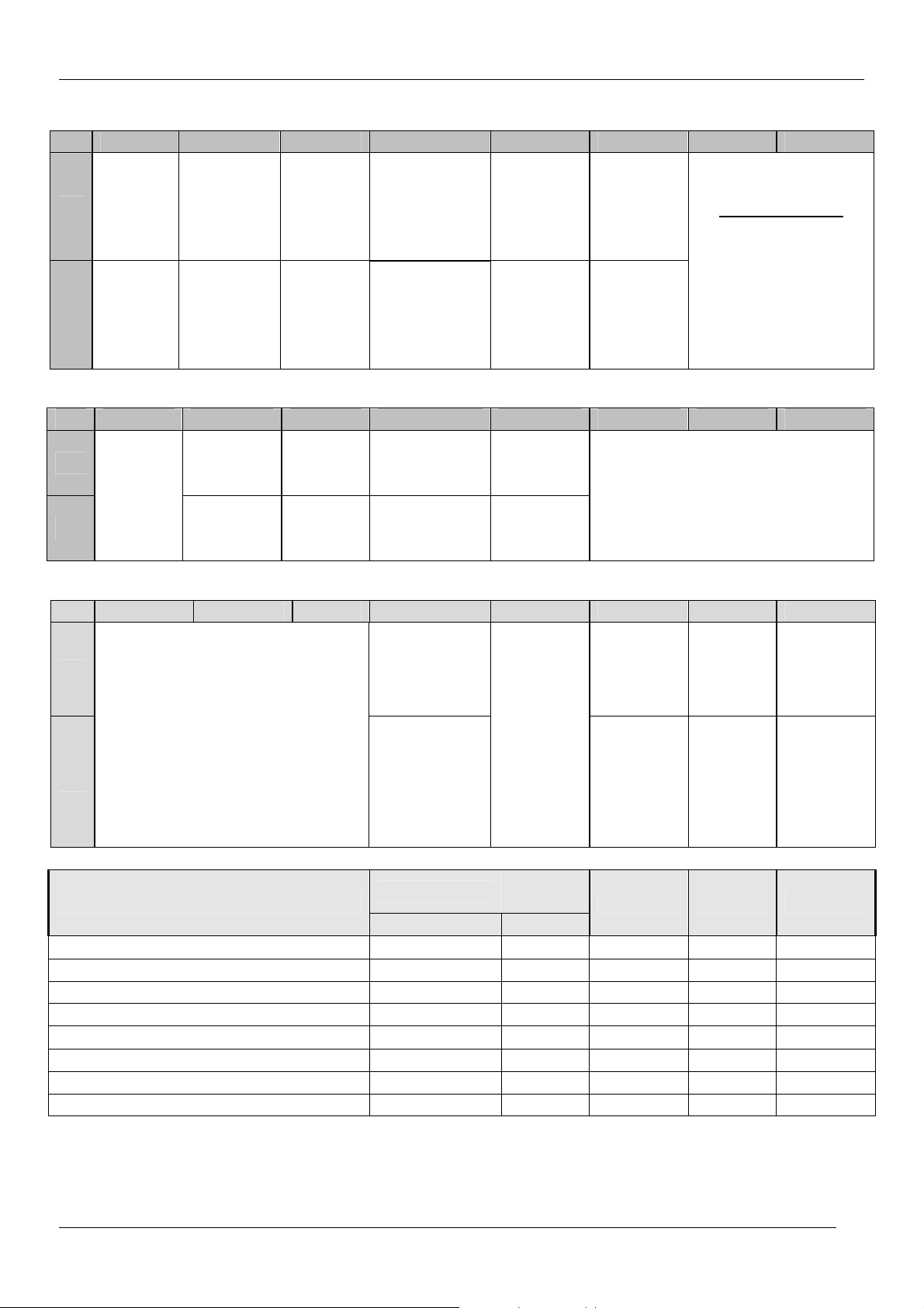
Pin Name I/O Description
1 VDDDACY S DAC(Y)
2 AYOUT O Y output
3 VSSDACY S DAC(Y)
4 VSSD2 S Supply voltage for digital (0V digital)
5 VDDD2 S Supply voltage for digital(1.8V digital)
6 SDA I/O I2C-Bus data
7 TMS I Testmode select (Connected to vdd33)
8 656VIN/BLANK I/O Separate V input for 656 / BLANK output
9 656CLK I/O Digital input / output clock
10 656IO7 I/O Digital input / output (MSB)
11 VSSP2 S Supply voltage for digital (0 V pad)
12 VDDP2 S Supply voltage for digital (3.3 V pad)
13 SCL I I2C-Bus clk
14 V I Vertical pulse for RGB input
15 656IO6 I/O Digital input / output
16 656IO5 I/O Digital input / output
17 HOUT O Horizontal output
18 H50 O Hout 50 Hz
19 ADR / TDI I I2C address / test data in
20 V50 O Vout 50 Hz
21 656IO4 I/O Digital input / output
22 656IO3 I/O Digital input / output
23 VOUT O Vertical output
24 RESET I Reset input (Reset active low)
25 VDDP3 S Supply voltage for digital (3.3 V pad)
26 VSSP3 S Supply voltage for digital (0 V pad)
27 CLKOUT O Output clock (27 MHz nom.)
28 VDDD3 S Supply voltage for DRAM (1.8 V digital)
29 VSSD3 S Supply voltage for digital (0 V digital)
30 656IO2 I/O Digital input / output
31 656IO1 I/O Digital input / output
32 656IO0 I/O Digital input / output (LSB)
CP-850FX Service Manual
Europe R&D
23

CP-850FX Service Manual
33 VSSD4 S Supply voltage for digital (0 V digital)
34 VDDD4 S Supply voltage for digital 1.8 V digital
35 VDDAFBL S Supply voltage for FBL (1.8 V)
36 VSSAFBL S Supply voltage for FBL (0 V)
37 FBL1 I Fast Blank input 1 (H1) (Analog input)
38 FBL2 I Fast Blank input 2 (H2) (Analog input)
39 RIN1 I R or V in1 (Analog input)
40 GIN1 I G or Y in1 (Analog input)
41 BIN1 I B of U in1 (Analog input)
42 VDDARGB S Supply voltage for RGB (1.8 V)
43 VDDARGB S Supply voltage for RGB (0 V)
44 VDD33RGB S Supply voltage RGB (3.3 V)
45 VDD33RGB S Supply voltage RGB (0 V)
46 RIN2 I R or V in2 (Analog input)
47 GIN2 I G or Y in2 (Analog input)
48 BIN2 I B of U in2 (Analog inpu)
49 VSSD5 S Supply voltage for digital (0 V)
50 VDDAC1 S
51 VSSAC1 S Supply voltage CVBS1 (0 V)
52 CVBS1 I CVBS input (Analog input)
53 CVBS2 I CVBS input (Analog input)
54 CVBS3 I CVBS input (Analog input)
55 CVBS4 I CVBS input or Y1 (Analog input)
56 CVBS5 I CVBS input or C1 (Analog input)
57 CVBS6 I CVBS input or Y2 (Analog input)
58 CVBS7 I CVBS input or C2 (Analog input)
59 VDD33C S Supply voltage CVBS (3.3 V)
60 VSS33C S Supply voltage CVBS (0 V)
61 CVBSO3 O CVBS output 3 (Analog output)
62 CVBSO2 O CVBS output 2 (Analog output)
63 CVBSO1 O CVBS output 1 (Analog output
64 VDDAC2 S Supply voltage CVBS2 (1.8 V)
65 VSSAC2 S Supply voltage CVBS2 (0 V)
66 VDDD1 S Supply voltage for digital (1.8 V digital)
67 VSSD1 S Supply voltage for digital (0 V digital)
68 VDDAPLL S Supply voltage for PLL (1.8 V)
69 XOUT O Crystal connection 2
70 XIN I Crystal connection 1
71 TCLK I Testclock
72 VDDP1 S Supply voltage for digital (3.3 V pad)
73 VSSP1 S Supply voltage for digital (0 V pad)
74 656HIN/CLKF20 I/O Separate H input for 656 / 20.25 clock output
75 VDDDACV S DAC (V)
76 AVOUT O V output
77 VSSDACV S DAC (V)
78 VDDDACU S DAC (U)
79 AUOUT O U output
80 VSSDACU S DAC (U)
Supply voltage CVBS1 (1.8 V) and digital core
supply
Europe R&D
24
CP-850FX Service Manual
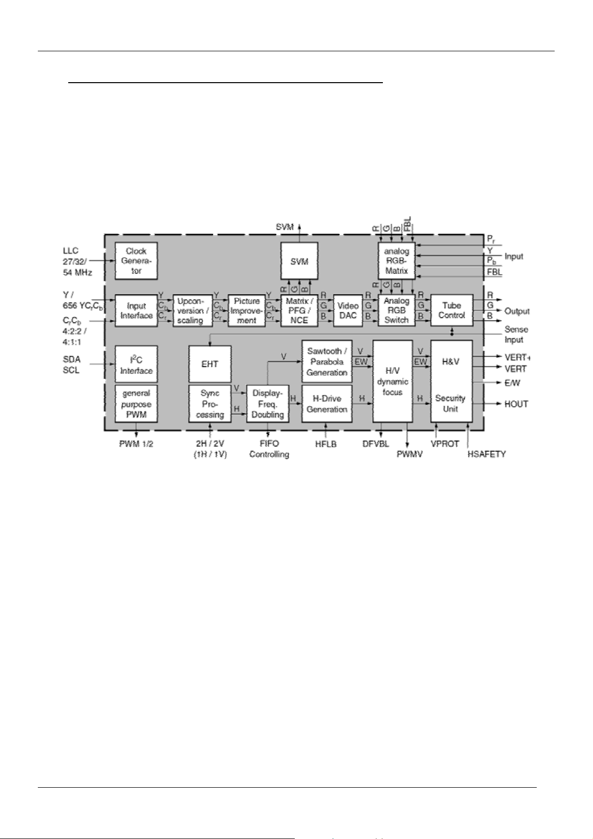
4.3 DDP 3315C – DISPLAY AND DEFLECTION PROCESSOR
The DDP 3315C is a mixed-signal single-chip digital display and deflection processor, designed
for high-quality backend applications in double scan and HDTV TV sets with 4:3 or 16:9 picture
tubes. The interfaces qualify the IC to be combined with state of the art digital scan rate
converters, as well as analog HDTV sources. The DDP 3315C contains the entire digital video
component, deflection processing, and all analog interfaces to display the picture on a CRT.
4.3.1 BLOCK DIAGRAM OF THE DDP 3315C
4.3.2 DESCRIPTION
Video Processing
– linear horizontal scaling (0.25 ... 4), as well as nonlinear horizontal scaling “panorama vision”
– dynamic black level expander
– luma sharpness enhancement by dynamic peaking and luma transient improvement (LTI)
– color transient improvement (CTI)
– programmable RGB matrix
– black stretch, blue stretch, gamma correction via programmable Non-linear Colorspace
Enhancer (NCE) on RGB
– two analog double scan inputs with fast blank (one RGB and one RGB/YC r C b /YP r P b
selectable)
– average and peak beam current limiter
– automatic picture tube adjustment (cutoff, drive)
– histogram calculation
Deflection Processing
– scan velocity modulation output
– digital EHT compensation for vertical / east-west
– soft start/stop of horizontal-drive
– vertical angle and bow correction
– differential vertical outputs
– vertical zoom via deflection adjustment
– horizontal and vertical protection circuit
Europe R&D
25

CP-850FX Service Manual
– horizontal frequency for VGA/SVGA/1080I
– black switch off procedure
– supports horizontal and vertical dynamic focus
Miscellaneous
– selectable ITU-R 601 4:1:1 / 4:2:2 YC r C b input at 27/32 MHz or double scan ITU-R 656 input
at 54 MHz line-locked clock
– crystal oscillator for horizontal safety
– picture frame generator
– hardware for simple 50/60 Hz to 100/120 Hz conversion (display frequency doubling)
– PQFP80 package, 5 V analog and 3.3 V digital supply
IC architecture
A clock generator converts different external line locked clock rates to a common internal sample
rate of ~40 MHz, in order to provide a higher horizontal resolution. The input interface accepts
ITU-R 601 at 27 or 32 MHz and ITU-R 656 with encoded or external sync at 54 MHz. The
horizontal scaler is used for the scan rate conversion and for the nonlinear aspect ratio conversion as well.
For the picture improvement, luma and chroma are processed separately. The luminance
contrast ratio can be extended with a dynamic black level expander. In addition the frequency
characteristic is improved by a transient improvement (LTI) and an adaptive dynamic peaking
circuit. The peaking adapts to small AC amplitudes of high frequency parts, while large AC
amplitudes are processed by the LTI. The chroma signal is enhanced with a transient
improvement (CTI) with proper limitation to avoid wrong colours.
The full programmable RGB matrix covers control of colour saturation and temperature. A digital
white drive control is used to adjust the white balance and for the beam current limitation to
prevent the CRT from over-load. A non-linear colorspace enhancer (NCE) for RGB gives full
flexibility for any amplitude characteristic.
High speed10-bit D/A converters are used to convert digital RGB to analog signals. Separate 9bit D/A converters control brightness and cutoff. For picture tubes equipped with an appropriate
yoke a scan velocity modulation (SVM) signal is calculated using a differentiated luminance
signal.
Two analog sources can be inserted in the main RGB, controlled by separate fastblank (FBL)
signals. Contrast and brightness are adjusted separately from main RGB. One input is dedicated
to RGB for on screen display (OSD). The second input is processed with an analog RGB matrix
to insert YC
/YpbPr or RGB with control of colour saturation and programmable half contrast.
bCr
The bandwidth of ~30MHz guarantees pixel based graphics to be displayed with full accuracy.
All previously mentioned features are implemented in dedicated hardware. An integrated
processor controls the horizontal and vertical deflection, tube measurement loops and beam
current limitation. It is also used to calculate an amplitude histogram of the displayed image.
The horizontal deflection is synchronized with two numeric phase-locked loops (PLL) to the
incoming sync. One PLL generates the horizontal timing signals, e.g. blanking and key-clamping.
The second PLL adjusts the phase of the horizontal drive pulse with a subpixel accuracy less
than 1 ns.
Vertical deflection and east/west correction waveforms are calculated as 6th order polynomials.
This allows adjustment of an east/west parabola with trapezoidal, pincushion and an upper/lower
corner correction (even for real flat CRT’s), as well as a vertical sawtooth with linearity and Scorrection. Scaling both waveforms, and limiting to fix amplitudes, performs a vertical zoom or
compression of the displayed image. A field and line frequent control loop compensates picture
content depending EHT distortions.
Europe R&D
26

CP-850FX Service Manual
4.3.3 PINNING
Pin No. Pin Name I/O Description Remarks
1 Y6 I Picture bus Luma
2 Y7 I Picture bus Luma (MSB)
3 656EN I Enable 656 input mode
4 LLC2 I System clock input
5 HS I Horizontal Sync Input
6 VS I Vertical Sync Input
7 FREQSEL I Selection of H-Drive Frequency Range
8 CM1 I Clock select 1
9 CM0 I Clock select 0
10 VS2 I Additionnal VSYNC input
11 XTAL2 O Analog Crystal Output
12 XTAL1 I Analog Crystal Input
13 NC
14 GNDP S Ground, Output Pin Driver
15 VSUPP S Supply voltage, Output Pin Driver
16 FIFORRD O FIFO Read Counter Reset
17 FIFORD O FIFO Read Enable
18 FIFOWR O FIFO Write Enable
19 FIFORWR O FIFO Write Counter Reset
20 PWM1 O I2C controlled DAC
21 PWM2 O I2C controlled DAC / Tilt output
22 PWMV O I2C controlled DAC
23 HOUT O Horizontal drive output
24 VSTBY S Standby supply voltage, Hout generation
25 DFVBL O
26 HSYNC O Horizontal sync output
27 VSYNC O Vertical sync output
28 NC
29 ASG1 S Analog Shield Ground
30 HFBL I Horizontal flyback input
31 SAFETY I Safety input
32 VPROT I Vertical protection input
33 RSW2 O Range Switch2, measurement ADC
34 RSW1 I/O Range Switch1, measurement ADC
35 SENSE I Sense ADC input
36 GNDM S Ground, MADC input
37 VERT+ O Differential Vertical Sawtooth Output
38 VERT- O Differential Vertical Sawtooth Output
39 EW O East / West Correction Output
40 NC
41 SVM O Scan Velocity Modulator
42 ROUT O Analog Output Red
43 GOUT O Analog Output Green
44 BUT O Analog Output Blue
45 GNDO S Ground, analog Back End
46 XREF I Reference Input for RGB DAC’s
47 VSUPO S Supply voltage, Analog Back End
Dynamic focus blanking / horizontal DAF
pulse
Europe R&D
27
 Loading...