

Daewoo CP-390 Service Manual


TABLE OF CONTENTS
1. SPECIFICATIONS ................................................................................................................................ 1
2. SAFETY INSTRUCTION ....................................................................................................................... 2
3. BLOCK DIAGRAM ................................................................................................................................ 3
4. ALIGNMENT INSTRUCTIONS ............................................................................................................. 4
5. IC DESCRIPTION ................................................................................................................................. 7
6. CIRCUIT DESCRIPTION ...................................................................................................................... 35
7. PCB LAYOUTS...................................................................................................................................... 44
7-1. PRINTED CIRCUIT BOARD
7-2. SCHEMATIC DIAGRAM
8. TROUBLE SHOOTING CHARTS ......................................................................................................... 46
9. IC DC VOLTAGE CHARTS ....................................................................................................... ........... 53
10. ELECTRICAL PARTS LIST .... .......................................................................................................... .. 56
11. CP-390 (INDIA CRT) INCH DIFFERENCE PART LIST...................................................................... 74
12. CP-390(ORION CRT)INCH DIFFERENCE PART LIST ..................................................................... 75
13. CP-390 CHASSIS CRT DIFFERNT PART LIST ................................................................................. 76
1. SPECIFICATIONS
TV STANDARD PAL/SECAM-B/G, D/K, I, H, NTSC-3.58/4.43/5.5
MA INS V O LTAG E 100~250V AC , 50/60Hz
POWER CONSUMPTION 14T6VM=72W
20T6VM=82W
21T6VM=87W
SOUND OUTPUT 14” : 3W+3W
20” : 5W+5W
21” : 8W+8W
SPEAKER 14” : 5W 8 0hm(2EA)
20” : 5W 8 0hm (2EA)
21” : 8W 8 0hm (2EA)
ANTENNA
IMPEDANCE
TUN ING SY STE M Voltage Synthesize tuning System
ME M O RY C HA NN EL VM : 100 channels, TM : 70 channels
RECEPTION
CHANNEL UNIT
RE M OT E C O NT RO L VM : R-28B04, TM : 28B03
SCREEN SIZE
W EIGHT 14” : 9.7Kg(set)
INDICATION On-Screen Display
75 ohm unbalanced
300 ohm balanced with supplied balun
VHF - L : CH2 - CH4
VHF - H : CH5 - CH12
Cable Band : CHS1’ - CHS3’, CHS1 - CHS20
Hyper Band : CH S21 - CHS 40(option)
UHF : CH21 - CH69
14” : 34cm (A34JLL 90 02)
20” : 48cm (A48JLL 90 02)
21” : 51cm (A51JLL 90 02)
20” : 18.5Kg(set)
21” : 27.2Kg(set)
MENU
Picture(Bright, Color, C ontra st, Sharpness, TINT)
T im e r( C lo ck , Wa ke - up - T im e , A c tiv ate , Wa k e -u p -P ro g )
Language
Preset
Edit
Sleep Tim er
AV
Sound Mute
Volume Control
1

2. SAFETY INSTRUCTION
WARNING
:
Before servicing this chassis, read the “X -RAY radiation precaution”,
“safety precaution” and “product safety notice” below.
2-1. X-RAY RADIATION PRECAUTION
1. Excessive high voltage can produce potentially hazardous X-RAY R ADIATION.To avoid such hazards,
the high voltage must not exceed the specified lim it. The nominal value of the high voltage of this receiver
is 22-23kv(14”), 25-26kv(20”, 21”) at max beam current. The high voltage must not,
under any circumstances, exceed 27.5kv (14", 20”), 29.0kv(21”).
Each tim e a receiver requires servicing, the high voltage should be checked. It is recommended the
reading of the high voltage recorded as a part of the service records. it is important to use an accurate and
reliable high voltage meter.
2. The only source of X-RAY R adiation in this TV receiver is the picture tube. For continuous RADIATION
protection, the replacement tube m ust be exactly the same type tube as specified in the parts list.
2-2. SAFETY PRECAUTION
1. Potentials of high volt age are present when this receiver is operating. Operation of the receiver outside the
cabinet or with the back cover removed involves a shock hazard from the receiver.
1) Servicing should not be attempted by anyone who is not thoroughly familiar with the precautions
necessary w hen working on highvoltage equipment.
2) Alw ays discharge the picture tube to avoid the shock hazard before rem oving the anode cap.
3) Discharge the high potential of the picture tube before handling the tube. The picture tube is highly
ev a c u a te d a n d if b ro k e n , g la s s fr a gme n ts w ill b e v io le n tly e x p e lle d .
2. If any Fuse in this TV receiver is blown, replace it with the FUSE specified in the Replacement Parts List.
3. When replacing a high wattage resistor(oxide m etal film resistor) in circuit board, keep the resistor
10mm away from circuit board.
4. Keep wires away from high voltage or high temperature com ponents.
5. This receiver must operate under AC260 volts, 50Hz/60H z.
(AC 100~250 volts, 50/60Hz)NEVER connect to DC supply or any other power or frequency.
2-3. PRODUCT SAFETY NOTICE
Many electrical and mechanical parts in this chassis have special safety-related characteristics.
These characteristics are often passed unnoticed by a visual inspection and the X -RAY RA DIATION
protection afforded by them cannot necessarily be obtained by using replacement components rated for
higher voltage, watt a ge, etc. Replac ement parts whic h hav e these specia l safet y c ha racteristics are identified
in this manual and its supplements, electrical components having such features are identified by designated
symbol on the parts list. Befor e replacing any of t hes e c omponent s , read the parts list in thi s manual c areful ly.
The use of substitute rep lacement parts which do not have the same safety characteristics as specified in t he
parts list may created X-RAY Radiation.
2
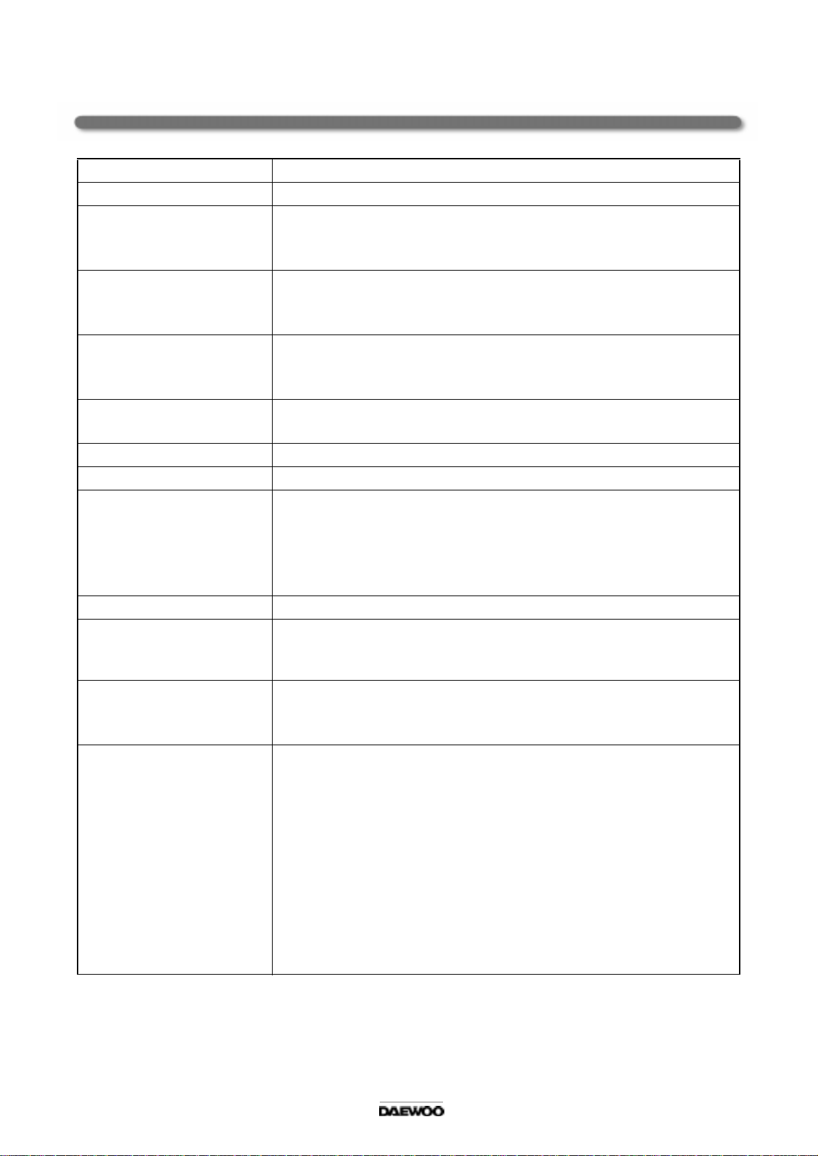
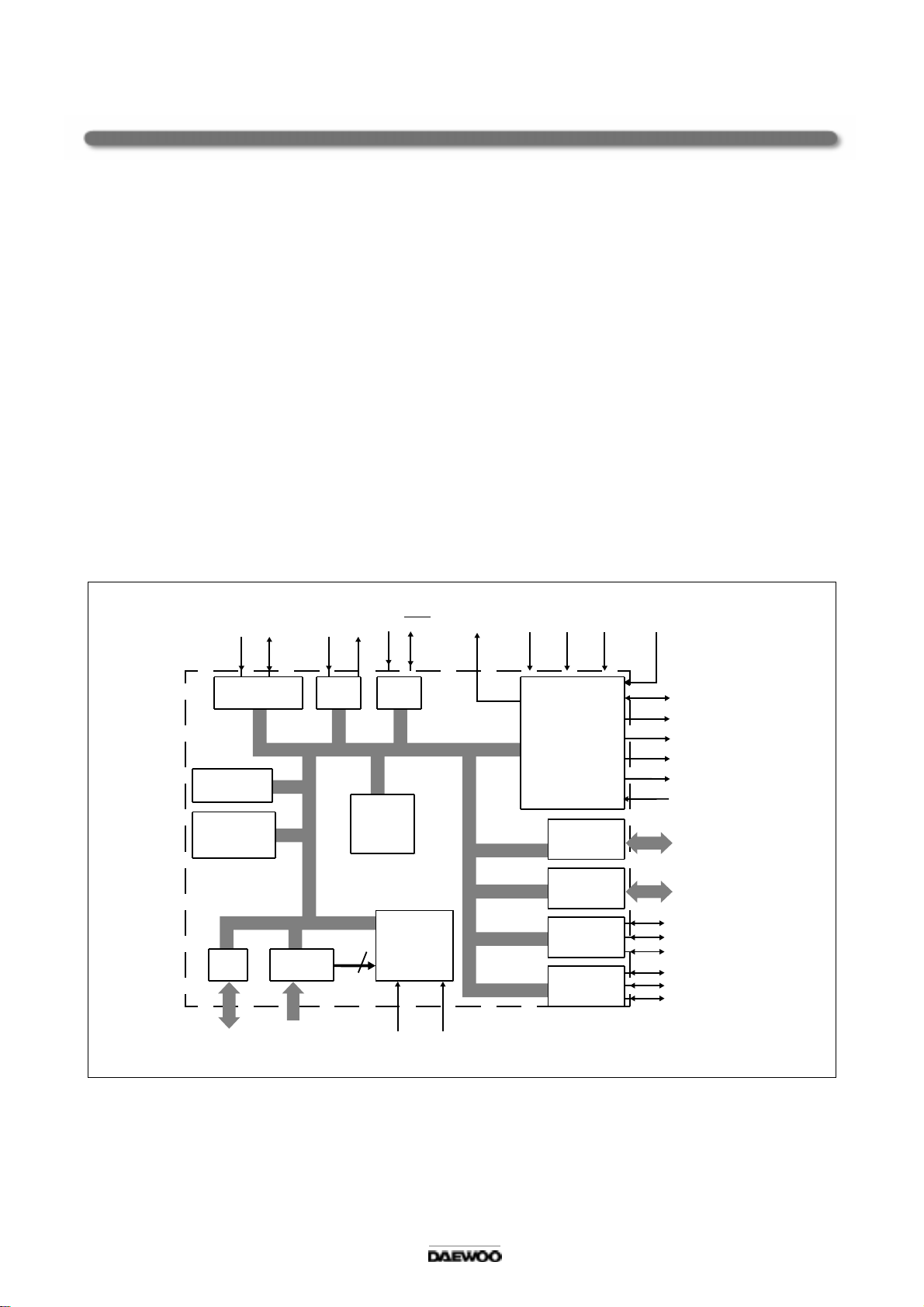
3. BLOCK DIAGRAM
3
4. ALIGNMENT INSTRUCTIONS
4-1. AFT
1. Standard B/G, D/K, I
1) Set a S ignal Generator with
- RF FREQ UEN CY = 38.9 MHz,
- RF OUTPUT LEVEL = 80
- System = PAL / SECAM - B/G , D/K, I
NT S C - 3 .5 8 /4.4 3
2) Connect the Signal Generator RF Output to P101 (Tuner IF Output).
There must be no signal input to the tuner.
3) Press the “AFT” KEY and wait until the TV screen display “AFT OK”.
2. AGC
1) Set a Pattern Generator with RF LEVEL 632 dBuV .
2) Connect a O SCILLOSC OP E PRO BE to P101 (TUNER AGC INPUT).
3) Adjust AGC UP/DOW N KEY the voltage drop 3.5V dc point its m aximum voltage.
(TDA8374A N1 V ER SION)
Adjust AGC up/down key the voltage drop 1V dc over blow its maximum voltage
(TDA8374A n3 version)
5 dBuV
Alternative Method
1) S e t a P atte rn G e n er a tor w ith
- RF LEVEL 80
5 dBuV
- PAL CROSSHATCH
( without SOUND CARRIER )
2) Connect a O SCILLOSC OP E
( Bandwidth
100MHz ) PROBE
to P 1 0 1 (TU NER IF OU TP UT ).
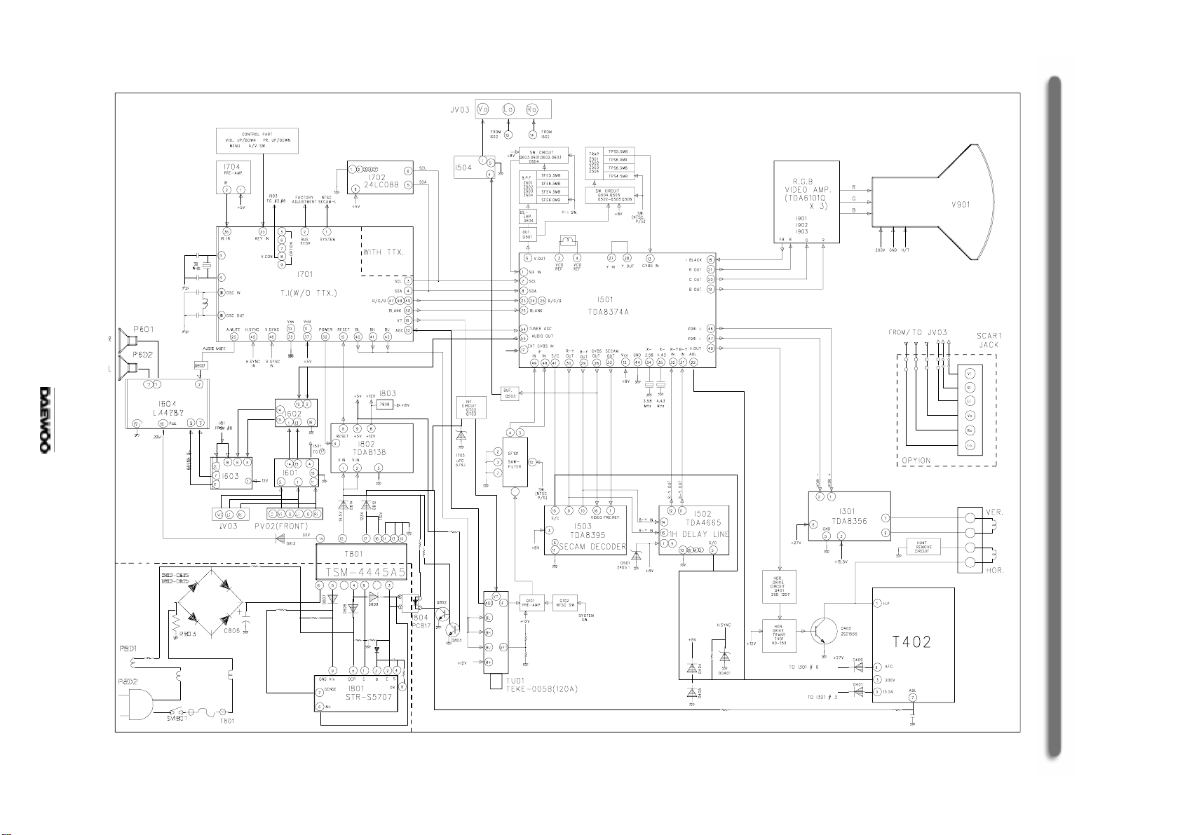
3) Use AGC UP/DO WN KEY to obtain
an envelop amplitude 200 + 50 mVp-p.
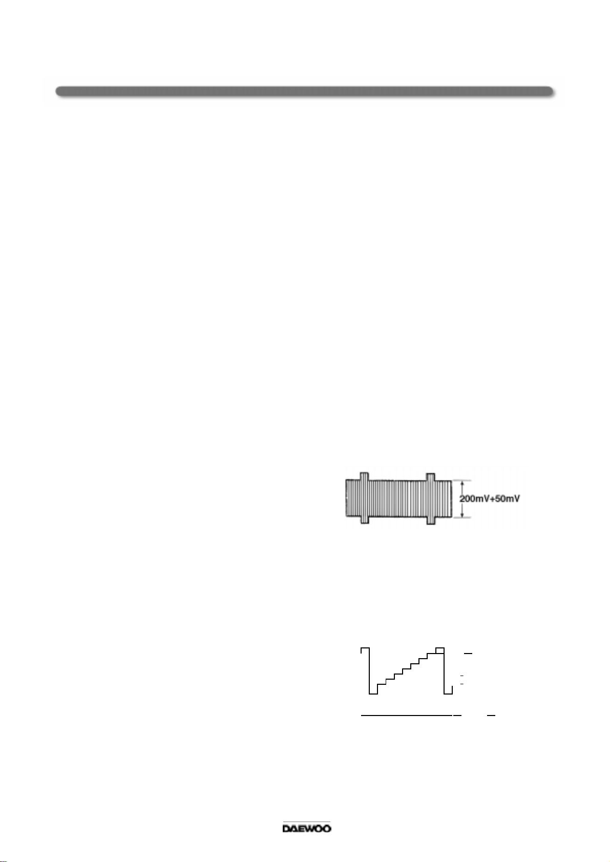
3. SCREEN
1) Apply a CO LOR BAR pattern signal.
2) Set the CONTRAST, BRIGH TNESS
to MAX , CO LOR to MIN .
3) Set the R,G,B LEVEL to CENTER (31/63)
160
5Vdc ( 20”, 21” ) with R,G,B UP/DOW N KEY.
4) Connect a O SCILLOSC OP E PRO BE
to P 9 0 4 ( CRT C A T H OD R , G , B ).
5) Adjust the SCREEN VOLUME on FBT
such that the highest black level voltage
160
5Vdc (20”, 21”), 1305Vdc (14”).
Black leve
160 + 5Vdc(20", 21")
130 + 5Vdc(14")
GND
4
4. WHITE BALANCE
1) S e t th e TV to N OR I mod e.
2) Set the R,G,B LEVEL to CENTER with R,G ,B UP/DOW N KEY .
3) Adjust the R,G,B UP/ DOWN KEY of the ot he r c o lor which did not appear on the s cr een t o obt ai n WHITE.
5. FOCUS
1) Apply a R ETM A PATT ERN signal.
2) A d ju st th e FOCUS V OLU ME o n F B T to o b ta in o p tim a l res o lutio n.
6. GEOMETRY
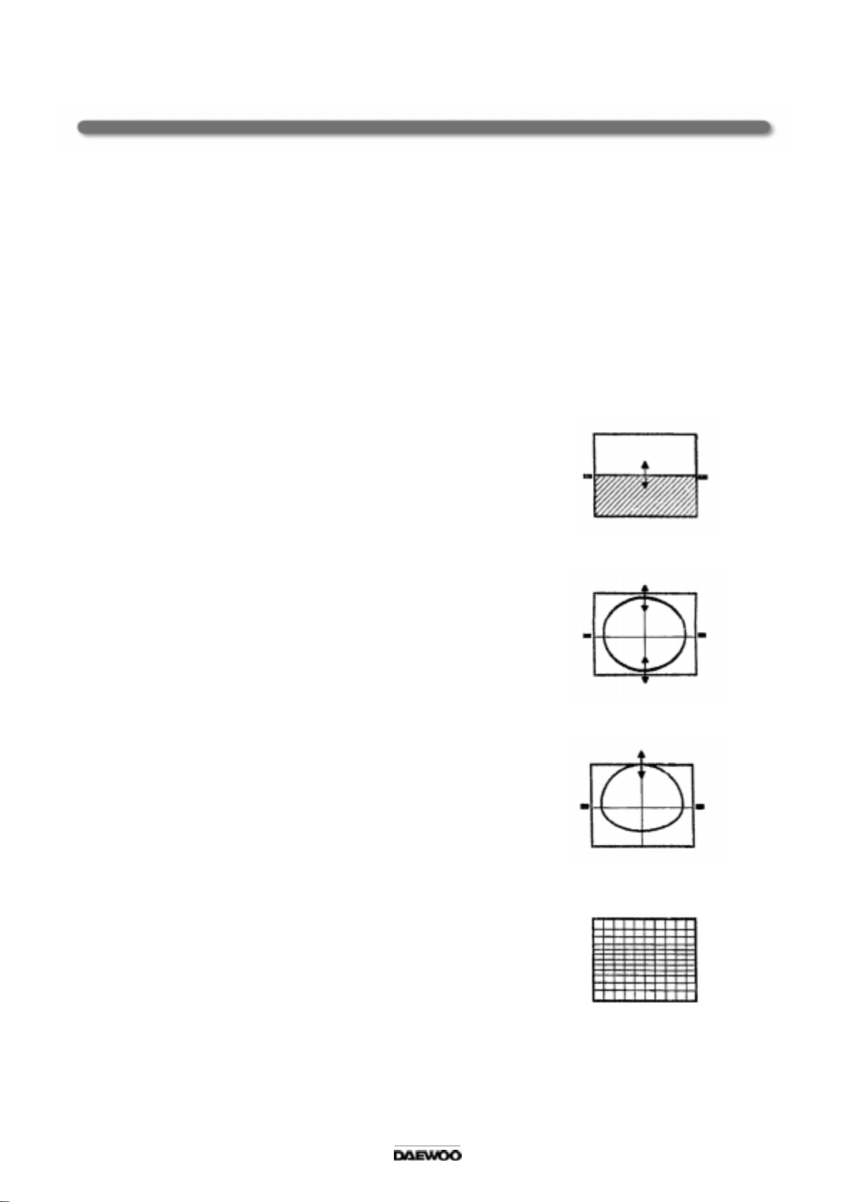
6.1 VERTICAL CENTER
1) S e t th e TV to N OR I mod e.
2) Pressing the V-SIZE UP/DOW N KEY,
the lower half of the screen is blanked.
3) Adjust the border line of blanked picture
coincident with the mechanical center marks
of the C RT using the V-CENTE R U P/DOW N KE Y.
6.2 VERTICAL SIZE
The VERT ICAL CENTE R adjustm ent
has to be done in advance.
1) Apply a R ETM A PATT ERN signal.
2) S e t th e TV to N OR I mod e.
3) Adjust the upper part of the picture
w ith th e V -S IZ E U P /D OWN k ey s.
6.3 VERTICAL SLOPE
The VERT ICAL SIZE adjustment
has to be done in advance.
1) Apply a R ETM A PATT ERN signal.
2) Adjust the lower part of the picture w ith
the V-SLOPE UP/DOWN keys.
6.4 VERTICAL S-C ORRECTION
1) Apply a CROSSHATCH PATTERN signal.
2) A d ju st th e S -C O R U P/DOW N KE Y to o bta in
the same distance between horizontal lines.
6.5 HORIZONTAL CENTER
1) Apply a R ETM A PATT ERN signal.
2) Adjust picture centering with H -CENTE R
LE F T /R IGHT k e ys .
5
If EEPROM(1703) has been changed ;
- Option data has to be changed and
- all alignment function has to be readjusted.
The initial state of adjustment are as follows;
- V-Center, V-S lope V-Size, H-Center, R , G, B, AFT = Center (30/64 - 33/64)
- S-Correction = 00/64
- AGC = 15~60/64
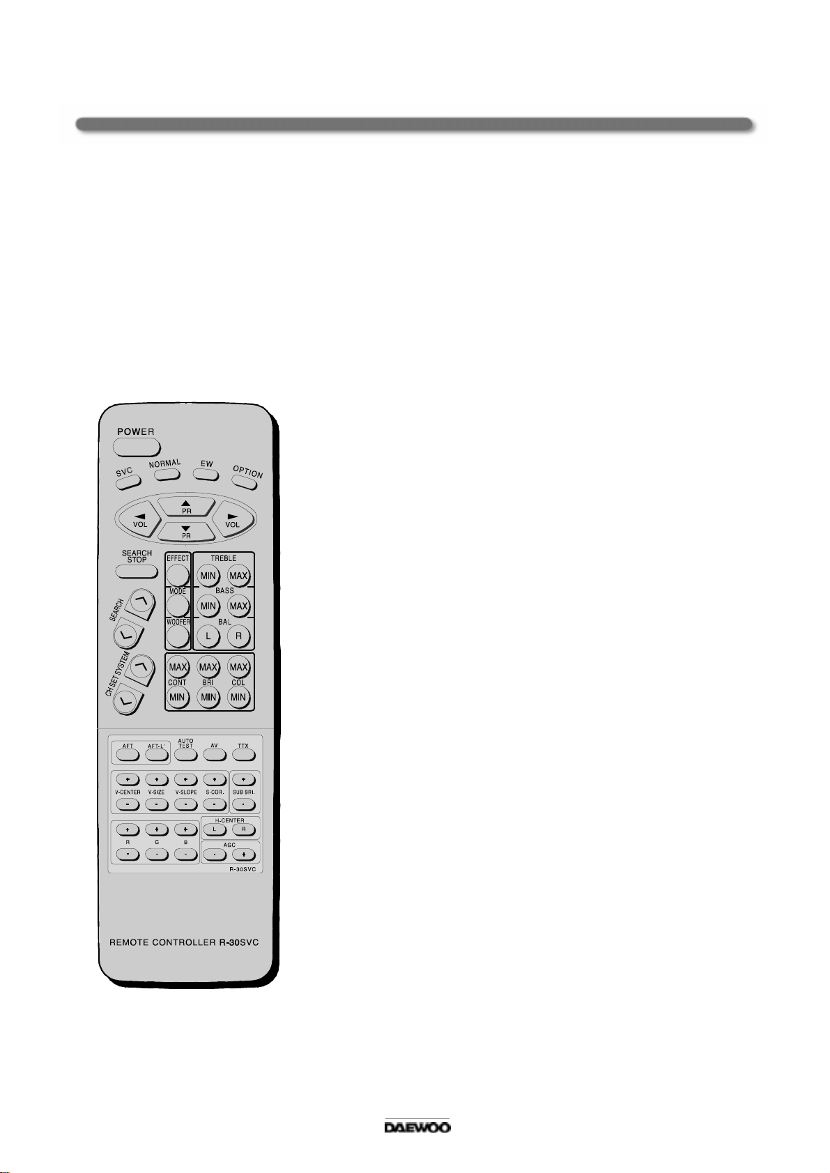
Service Remocon
6

5. IC DESCRIPTION
DW370ASM* (Micro-controller for Non-Teletext Model)
=TMS370C08A05 ( TI Type No.)
1. General Description
The TMS370C 08A05 devices are mem bers of the cMCU 370 family single-chip m icrocontrollers.
The cMCU370 famil y provides cost ef fect ive real-time system control through use of the PRISM methodology.
The PRISM m ethodology m odular fabrication process integrates analog, digital, linear and power
technologies on a single chip, thereby m aximizing the total integration strategy.
The TMS370C 08A05 devices are designed with the high-performance 8-bit TM S370C8 C PU.
Features of the ‘C8 CP U and system m odule as implemented on this device include three CPU registers
(stack pointer, status register, and the program counter), two external interrupts, reset,
mem ory mapped control registers.
2. Feature
• Inte rn al Memo ry C o n figu ra tion s
- 16K-Byte ROM Program Memory
- 512-B yte RAM
• Operating Features
- Supply Voltage (VCC) 5 V
- Input Clock Frequency 2, 20MHz
- Industrial Temperature Range
• Device Integrity Features
- Address Out-of-Range Reset
- Stack Overflow R eset
- Parallel Signature Analysis (C RC)
• Two 16-Bit G eneral P urpose Tim er(T8A)
Each Includes:
- 16-Bit R esettable Counters with individual 8-B it Prescaler
- 2 PWM Channels or
- 2 Input Captures or
- 1 Input Capture and 1 PWM Channel
• One 14-Bit PWM M odule
- 14-Bit R esettable Counters
- 14-B it PWM O utpu t Po rt
• One 8-Bit PWM M odule
- 8-Bit R esettable Counters
- 8-Bit PW M O utput P ort with 12V O pen Drain
• O S D Mo d u le
- Blanking/ Contrast reduction out
- Transparent Background
- Transparent Foreground
- Full Screen Background Color
10%
7
- Controlled Color, Blink, Size, Smoothing, Fringe of Each lines of C haracter
- Two size of different Font 12
- OSD W indow Display with 40
10 and 1218 by Hard Masking
25 lines
• 8-B it A /D Converter With 3 Inputs
- Single or Dual C hannel Operation
- Single or Continuous Conversion Modes
• Fle x ible Inte rru p t H a nd ling
- Global and Individual Interrupt Masking
- 2 S/W P rogramm able Interrupt Levels
- 2 External Interrupt (1 Non-Maskable)
- Programmable Rising or Falling Edge Detect
• 09 CMOS Compatible I/O Pins
- All Peripheral Function Pins Software Configurable for Digital I/O
- 6 Bidirectionals, 3 Input Pins
• Plastic 42 YSDP Pins Package
3. Block Diagram
INT1/VPP INT2 OSCIN OSCOUT TEST RESET O SCOUT_OSD OSCIN _OSD V-SYNC H-SYNC VCC_OSD
Interrupt
RAM
512-byte
EPROM/ROM
Program Memo ry
16K-byte
Port A
Port B
Multipiexed
With AN0-AN3
63
1/2 Clock
Oscillator
System
Control
TMS3 70C8
CPU (C8)
A-to-D Converter
3
VCC VSSB0/AN0-B2/AN2AO-A5
(ADC)
OSD
8 bit PWM
14 bit PW M
Tim e r 1 (T 8A 1 )
Timer 2 (T8A2)
6
2
COR
BLANK
RED OUT
GREEN OUT
BLUE OUT
VSS_OSD
PWM1_0/5
PWM2_0/1
T8A1IC1/CR
T8A1IC2/PWM1
T8A1IEVT/PWM
T8A2IC1/CR
T8A2IC2/PWM1
T8A2EVT/PWM
8

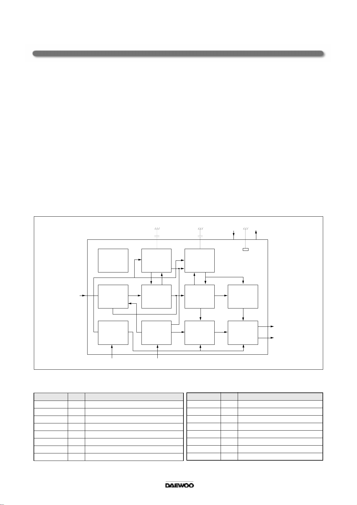
DW5255M*(Micro-controller & West/East Teletext Decoder)
DW5255RM*(Micro-controller & Cyrillic Teletext Decoder)
=SDA5255-A*** (SIEMENS Type No.)
1. General Description
The TDA5255 contains a slicer for VPS and TTX, an accelerating acquisition hardware module, a display
generator for “LEVEL 1” TTX data and a 8 bit u-controller running at 333 nsec cycle time.
The controller with dedicated hardware guarantees flexibility, does most of the internal processing of TTX
acquisition , t ransfers data to/from the external memory interface and receives/transmits data via I2C and
U A R T u se r inte rfa ce s .
The Slicer combined with dedicated hardware stores TTX data in a VBI 1Kbyte buffer.
The u-controller firm w are does the total acquisition task (ham m ing- and parity -checks,
page search and evaluation of header control bits) once per field.
2. Feature
• A cq u isition :
- feature selection via special function register
- sim ultaneous reception of TTX and VPS
- fixed framing code for VPS and TTX
- programm able framing code window for TTX
- Acquisition during VB I
- dire c t ac ce s s to V B I R A M bu ffe r
- Acquisition of packets x/26, x/27, 8/30 (firm w are)
- assistance of all relevant checks (firmware)
- 1-bit framing-code error tolerance (switchable)
• Display:
- features selectable via special function register
- 50/60 H z display
- level 1 serial attribute display pages
- blanking and contrast reduction output
- 8 direct addressable display pages
- 12 x 10 character m atrix
- 96 character ROM (standard G0 character set)
- 143 national option characters for 11 languages
- 288 characters for X/26 display
- 64 block mosaic graphic characters
- 32 free addressable characters for OSD in expanded character ROM + 32 inside OSD box
- double height (TOP/BOTTOM )
- conceal/reveal
- transparent foreground/background -inside/outside of a box
- cursor (colour changes from foreground to background colour)
- flash (flash ra te 1 s)
- programm able horizontal und vertical sync delay
9
- hardware assisted fast display page erase
- full screen background colour in outer screen
• Synchronization:
display synchronization to sandcastle or Horizontal Sync (HS) and Vertical Sync (VS) with
star ts to p -o s c illa to r or d ispla y s y n c h ro n iz a tio n to s andcastle or Horizontal Sync and Vertical Sync with
external clock independent clock systems for acquisition, displa y and con troller
• C on tro ller:
- 8 bit co nfiguration
- 20 MHz internal clock
- 0.33 us instruction cycle
- eight 16-bit data pointer registers (DPT R)
- tw o 16 -b it tim ers
- watchdog timer
- serial interface (UART)
- 256 bytes on-chip R AM
- 1 Kbyte on-chip extended RAM (access via M O VX)
- 8 Kbyte on-chip ACQ -buffer-RAM (access via MO V X)
- 6 channel 8-bit pulse width m odulation unit
- 2 channel 14-bit pulse width m odulation unit
- 4 multiplexed AD C inputs with 8-bit resolution
- one 8-bit I/O port with open drain output and optional I2C em ulation
- tw o 8-bit multifunctional I/O ports
- one 4-bit port w orking as digital or analog inputs
- one 2-bit I/O port with optional address latch enable function
• P -S D IP 5 2 p a c ka ge
• 5 V supply voltage
3. Block Diagram
10
4. Pin Descriptio n
(A* : D W5255M */DW5255RM *, B* : DW370AS M *)
Pin Name Symbol Descriptio n
A* B* A* B* A* B*
1
1 P 3 .1 T1 IC1/ C R S Y S N TSC O UT for switc h in g SA W filte r
2 2 P0.7/Open Drain A0 BU SS TO P I2C BUS STO P IN for Com puter
3 3 P0.6/Open Drain A1 SDA Serial data IN/OUT for I2C
4 4 P0.5/Open Drain A2 SCL Serial clock IN/OU T for I2C
K6259
- PAL/SECAM : L
- N TS C : H
controlled alignm ent in Factory
( A c tiv e L o w )
5 5 P0.4/Open Drain A3 O PTION #5 #6 Teletext
6 6 P0.3/Open Drain A4 O PTION
7 7 P0.2/Open Drain A5 OPTION Not Used
8 8 P0.1/Open Drain PWM 1-0/ Open D rain OP TION Not Used
9 9 P0.0/Open Drain PWM 1-1/ Open D rain LED LED drive OUT
10 10 VSS VSS ground
11 11 VC C VCC Power Supply
12 12 XTA L1 OS CIN OS CIN Input to inverting osc. Amplifier
13 13 XTA L2 OS CO U T OS CO U T Output of inverting osc. Amplifier
14 14 P4.0/ALE PW M 1-2/Open D rain N ot Used H : I/M, L : B/D
15 15 RE SET RES E T/Open D rain RST RE SET IN (ACTIVE LOW)
16 16 P1.7/14BIT PW M PW M 2-0 VT TUN ING V OLT AG E O UT
17 17 P 1.6 /14 B IT PWM P WM 2 -1 S W H : I/M
H H Wes t T e le tex t
L H E a s t Te le te x t
H L T urkish Teletext
- Stand-by mode : H
- Operating mode : L
( IR reception : pulse )
L : B/D
#6
H : STAND-BY
L : POW E R ON
Not Used
18 18 P1.5/8BIT PWM PW M 1-3/Open D rain F/SW Not Used
19 19 P1.4/8BIT PWM PW M 1-4/Open D rain N ot Used
20 20 P1.3/8BIT PWM PW M 1-5/Open D rain MU TE AU DIO M U TE O UT
21 21 P1.2/8BIT PWM TES T GN D (Must be tied 0V for DW 370M *)
22 P1.1/8BIT PW M Not Used
11
Pin Name Symbol Descriptio n
A* B* A* B* A* B*
23 P1.0/8BIT PW M Not Used
24 VSSA VSSA Analog GND for Slicer
25 FIL3 FIL3 PLL Loop Filter I/O for Phase Shifting
26 FIL2 FIL2
27 FIL1
FIL1
PLL Loop Filter I/O for TTX S licing
PLL Loop Filter I/O for VPS Slicing
28 VC C A VCC A Ana log Supply for Slice r
29 IREF IREF Reference Curren t for Slicer PLLs
30 CVBS CVBS CVBS IN
31 P2.3/8 bit AD C Not Used
32 22 P2.2/8 bit ADC B0/AN0/ADC AGC IF AGC INPUT for Auto Tuning System
33 23 P2.1/8 bit AD C B 1/AN1/ADC KS Local KEY SC AN IN
34 24 P2.0/8 bit AD C B 2/AN2/ADC S/SW Not Used
35 25 VSS VSS-OSD VSS Ground
36 2 6 P 3 .3 /INT1 IN T 1 IR R EMO T E IR IN
37 27 VD D VCC -OS D VD D Power Supply
38 28 LCIN OS CIN-OSD LCIN CLO CK IN for OSD
39 29 LCOUT OSCOUT-OSD LCOUT CLOCK OUT for OSD
40 30 P3.7/TXT I/O T2EVT/PWM 2 BL BAND VHF-L OUT ( Active High )
41 31 P3.6/RXD T2 IC2/PWM 1 BH BAND VH F-H O UT ( Active High )
42 32 P3.5/T1 T2IC1/CR BU BAND UHF OUT ( Active High )
43 33 P3.4/T0 T1EVT/PW M2 POWER POWER CONTROL OUT
44 34 P3.2/IN T0 INT2 Not Used
45 35 HS/SC HSYNC HSYNC HOR. SYNC. IN(Active High)
46 36 P4.7/VS VSY NC VSY NC VER T. SYN C. IN(Active H igh)
47 37 R R RE D O U T
48 38 G G GR EEN O UT
49 39 B B BLUE OU T
50 40 BLAN K BL B LAN K O UT
51 41 COR COR Not Used
(CONTRAST REDUCTION OUT)
52 42 P3.0 T1C2/PW M 1 EVEN/
ODD
12
EVE N/OD D O UT for non-interlacing
in T TX m o de
I702 24LC08B (EEPROM)
1. Features
• Single supply w ith operation down to 2.5V
• Low power CMOS technology
- 1mA active current typical
A standby current typical at 5.5V
- 10
A standby current typical at 3.0V
- 5
• Organized as two or four blo cks of 256 bytes (2
2 CTM
• Two wire serial interface bus, I
• Schmitt trigger, filtered inputs for noise suppression
• Output slope control to elim inate ground bounce
• 100KHz(2.5V) and 400KHz(5V) compatibility
• Self-timed w rite cycle(including auto-erase)
• P ag e -w rite bu ffe r fo r up to 1 6 b y tes
• 2ms typical write cycle time for page-w rite
• H ar dw a re w rite pr ote ct fo r e n tire mem o ry
• Can be operated as a serial ROM
• Factory programming(QTP) available
• ESD protection > 4,000V
• 1,000,000 ERASE /WRITE cycles(typical)
• D ata re te ntio n > 4 0 ye a rs
• 8-pin DIP, 8-lead or 14-lead SO IC packages
• Available for extended temperature ranges
- Comm ercial : 0°C to + 70°C
- Industrial : -40°C to + 85°C
co mpat ib le
2568) and (42568)
2. General Description
The Microchip Technology Inc. 24LC08B is a 8K-bit Electrically Erasable PROM .
The device is organized as four blocks of 256x9bit mem ory w ith a two w ire serial interface. Low vo ltage
design permits operation down to 2.5 volts w ith standby and active currents of only
A and 1mA respectively.
5
The 24LC08B also has a page-write capability for up to 16 bytes of data.
The 24L08B is available in the standard 8-pin DIP surface m ount 80IC packages.
3. Block Diagram 4. Pin Description
I/O
CONTROL
LOGIC
SDA SCL
CC
V
SS
V
WP
MEMORY
CONTROL
LOGIC
XDEC
HV GENERATOR
EEPROM ARRAY
(4X256X8)
PAGE LATCHES
YDEC
SENSE AMP
R/W CONTROL
PIN SYMBOL DESCRIPTION
1-3 A0, A1, A2 Device Address lnputs
4 V ss Ground
5 SD A Serial Da ta/A dd res s
6 S CL Serial Clock
7WP
8 Vcc +5V Power supply
13

I501 TDA8374A (Single chip TV Processor for Negative modulation IF )
TDA8374 (Single chip TV Processor for Negative & positive modulation IF)
1.
General Description
The TDA8374(A) is I2C-bus controlled single chip TV processors which are intended to be applied in
PAL/N TSC television receiver.
The IC is m ounted in a S-DIL 56 envelope.
2. Feature
• IF
- Vision IF amplifier with high sensitivity and good figures for differential phase and gain
- PLL demodulator with high linearity offering the possibility fo r (s in g le s tandard) intercarrier stereo
audio application .
- Alignment PLL via I2C
- [T DA8374] Multistandard IF w ith negative and positive modulation, switchable via I2C
• A U D IO
- Alignment free multi standard PLL audio demodulator (4.5 to 6.5 M Hz.)
- Mono volume control
• V ide o
- Integrated luminance delay line
- Integrated chroma trap and bandpass filters (auto calibrated)
- Asymmetrical peaking circuit in the lum inance channel
- Black stretching of non standard CVBS or luminance signals
• C olo u r
- SECAM interface for application with SECA M add-on TDA8395.
• R G B
- R G B c on tro l (brig h tn es s, c o ntra s t, sa tu ratio n )
- Black current stabilization and white point adjustment
• Inp u t / O u tpu t
- Flexible video source select with CVBS input for the internal signal and two external video inputs
(one switchable for CVBS or Y/C).
- The output signal of the video source select is externally available
(also as CVBS when Y/C input is used).
- External audio input.
- Linear RGB input with fast blanking.
• Synchronization and Deflection
- Horizontal synchronization with two control loops and alignment free horizontal oscillator.
- Slow start and slow stop of the horizontal drive output to enable low stress start-up and
switch-off from the line circuit at nominal line supply voltage.
- Vertical count-down circuit for stable behavior with provisions for non-standard signals.
- Vertical geom etry control.
- Vertical drive optimized for DC coupled vertical output stages.
14
• C on tro l
- F ull I2 C b us co n tro l, as w e ll for c us to m e r c on tro ls a s for fa c tory a lign m e n t.
- All automatic controls have an option for forced m ode.
• Power consumption
- Low power consumption (900 mW at 8.0 Volts).
• Packaging
- SDIL-56 (Shrinked Dual In Line, 56 pins).
3. Pinning Diagram of Sdil-56
SOUND IF INPUT
EXT AUDIO INPUT
VCO R EF FILTER
VCO R EF FILTER
PLL LOO PF ILTER
IF VIDEO OU TP UT
BUSINPUT : SCL
BUSINPUT : SDA
BANDGAP DECOUPLING
CHROMA INPUT
Y/CYBS INPUT
MAIN POSITIVE SUPPLY
INT C Y B S IN P U T
GROUND
AUDIO OUT
DECOUPLING FILTER TUNNING
EXT CVBS INPUT
BLACK CURRENT INP
BLUE OUTPUT
GREEN OUTPUT
RED OUTPUT
Y-GUARD INP/BEAM CUR LIMITER
RED INPUT
GREEN INPUT
BLUE INPUT
RG B INSE R T IO N S WIT C H IN P
LUM INANC E INP UT
LUMINANCE OUTPUT
1
2
3
4
5
6
7
8
9
10
11
12
13
14
15
16
17
18
19
20
21
22
23
24
25
26
27
28
SDIL56
56
DECOUPLING SOUND DEMODULATOR
55
AUDIO DEEMPHASSIS
54
TUNER AGC OUTPUT
53
AGC DECOUPLING CAPACITOR
52
REREFERENCE CURRENT INPUT
51
VERT. SAWTOOTH CAPACITOR
50
EHT/OVERVOLTAGE PROTECTION INP
49
IF IN PU T
48
IF IN PU T
47
VERT. DRIVE NEG
46
VERT. DRIVE POS
45
EAST-WAST DRIVE
44
GROUND
43
PHI1 FILTER
42
PHI2 FILTER/FLASH PROT
41
SANDCASTLE OUTP/FLYBACK INP
40
HOR. OUTPUT
39
BLACK PEAK HOLD CAPACITO R
38
CVBS OUTPUT
37
POSITIVE SUPPLY
36
LOOPFILTER BURST PHASE DET
35
X-TAL (4.43/3.58)
34
X-TAL (3.58)
33
SECAM REF OUTPUT
32
(R-Y ) INP U T
31
(R-Y ) INP U T
30
(R-Y ) OUT PUT
29
(B-Y) OUT P U T
FIG 1 : Pinning diagram of SDIL-56
15
4. Block Diagram
16
5. Pin Descriptio n
No Name Description
1 SOUND IF INPUT The sound equivalent in put impedance is 8k5 ohm // 5pF wh ich has to be
tak e n into a c c o u n t fo r p rop e r te r min a t ion o f th e c e ra mic filte rs .
The DC impedan ce is very high.
The m inimum input signal for catching is l mV rms.
2 E XT A U DIO INPU T A n external sound signal (5 00m Vrm s) for example from S CA R T can be
applied to this pin via a coupling capacitor.
The input im peda nce is 25kohm.
3
VCO R EF F ILTER The IF VC O tuned circuit is applied to these pin.
4
5 P LL LOO P FILTER The PLL loopfilter is a first order filter with R=390 ohm and C = 100nF in
6 IF VIDEO O U TPU T A lthough the video output impedance is low it is recommen ded to avoid
7 B US I NPUT : SCL S e r ia l clo c k line
8 B US I NPUT : SDA Se r ia l da ta line
9 BANDGAP
DECOUPLING
10 CHROMA INPUT The supplied C S -VHS input burst amplitude should be nominally 300mV pp
11 Y/CVB S INPU T The Y S -VHS signal of 1V pp ( inclusive sync amp litude) is AC coupled to pin1 1.
12
37
MAIN
POSITIVE SUPPLY
Its resonance frequency must be two tim es the IF-frequency and in between a
range of 64-120MHz.
This range is suitable for the IF standards as 33.4, 38 .9, 45.75 and 58.75MH z.
The VC O frequency can be adjusted b y I2C bus so a fixed coil can be used.
serie s to ground.
The loopfilter bandwidth is 60kHz and is optimal for both fast catching and
sufficient video suppression for optimal sound perfo rmance.
Sound performance can theoretically be improved by adding a small
capacitor (approx.0- 4.7nF) betw een pin 5 and ground.
This however must be evaluated further because the normal video signal
response should not be effected.
high frequency current in the output due to for instance sound trap filters.
This can be achieved by m eans of an emitter follower at the video o utput with
resistor in series with the base
a 1
The bandgap circuit provides a very stable and temperature independent
reference voltage.
This reference voltage (6.7V) ensures optimal performance of the TDA8 374
and is used in almost all functional circuit blocks.
(assumed is a colour bar signal with 75% saturation and with chroma/burst
ratio of 2.2/1 ). The C S-VHS input is internally clamped to 4V via 50
The external AC coupling capacitor with 50
A recomm ended coupling capacitor is 1 nF; the high pass filter cut off
frequency is the n approximately 3K H z.
The TD A8374 ha s a m ain supply pin 12 and a horizontal supply pin 37. Both
pins have to be supplie d simultaneously.
Notice that the IC has not been designed to use this pin 37 as start pin.
(pin 37 supplies the horizonta l oscillator, PHI-1 and PHl-2)
(pin 12 supplies the rest of the circuits in the IC)
The nom inal supply voltage is 8V. With min/max values of 7.2-8.8V.
Also in stand-by condition the IC must be supplied with 8V.
A voltage detection circuit is connected to both pins.
- pin12 if V 12 <6.8V than a power on rese t, POR , is generated.
The Hout output is disabled immediate.
- pin37 if V37 <5.8V than the horizon tal output is disabled imm ediate.
.
forms a high pass filter.
.
17
No Name Description
13
17
14 G RO UN D All inte rnal circuits are connected to this ground pin 14.
15 AU D IO O UTP U T T he output signa l is volume controlled and is active fo r both internal and
16 DECOUPLING
18 BLACK CURRENT
19
20
21
22 V-GUARD INPUT/
INT CVBS INPUT
EXT CVBS INPUT
FILTER TUNING
INPUT
BLUE OUTPUT
GREEN OUTPUT
RED OUTPUT
BEAM CURRENT
LIMITER
It is recomm ended that the CVBS1 int and CVBS2 ext input am plitudes are
1 Vpp (inclusive sync amplitude).
This, because the noise detector switches the
(i.e . a u to
100mV rms (i.e. at S/N of 20dB).
external audio signals. The nominal gain is +9dB and -71dB, which gives
a total control range of 80dB.
The output signa l range therefor is 0.14- 1400mVrms
The bandw idth is >100kHz, the DC level is 3.3V and the output im pedance
is 2 5 0
Voltage variations at pin 16, which can be due to external leakage current or
crosstalk from interference sources, should be less than 50mV to ensure that
tuning of filters/delay cells remains correct.
For correct operation of the loop CURRENT inform ation is supplied to the
black current input pin.
The RG B outputs are supplied to the video output sta ges from pins 21, 20
and 19 respectively.
For nominal signals (i.e. C VBS/S-VHS, -(R-Y)/- (R-Y), TXT inputs) and for
nominal control settings, then the RGB output Signal amplitu des is
typically 2VBLACK_WHITE.
1mode w hen FOA , FOB = 0,0) when noise level exceeds
.
1 loop to slow mode
Vertical Guard
With this function, the correct working o f the vertical deflection can be
monitored. If the vertical deflection fails, the RGB outputs are blanked to
prevent damage to the picture tube.
Be a m cu rre nt limitin q
The beam current limiting function is realise d by reducing the contrast (and
finally the brightness) when the beam current reaches s too high level. The
circ u it fa lls a p a rt in tw o fun c tio n s :
- Average beam current limitin g (ABL): re acting on the average content of
the picture
- Peak white limiting (PWL): reacting on high local peaks in the RGB signal.
23
24
25
26 RGB INSERTION
27 LU M INAN CE INPU T An nom inal input signal am plitude of 1 Vblack-white MU ST b e DC coupled
RED INPUT
GREEN INPUT
BLUE INPUT
SWIT C H INPUT
The Rin, Gin, Bin input signals (nominal signal amplitude of 700mV ) are
AC coupled to pin 23, 2 4 and 25 respectively.
Clamping action occurs durin g burstkey period.
The table below a survey is given of the three modes which can be selected
with a voltage on R G B insertion switch input pin ;
V p in 2 6 I2 C fu n ctio n Se le c te d RGB s ig n a l
0.9 V - 3V IE 1 = 0 R GB(in te rn a l)
IE1 = 1 Rin ,Gin,B in
(fast insertion on pin23,24,25)
> 4 V IE 1 =X O SD c a n b e in s e rted a t the RGBo u t p in s
to the luminance input pin 27.
The pin is internally AC coupled to the luminance clamp via a capacitor of
50pF; clamping action occurs during burstkey period.
18
No Name Description
28 LUMINANCE
OUTPUT
29
30
31
32
33 SECAM REF
34
35
36 LO OP FILTER
38 CVBS OU TPUT The output amplitude is 1Vp-p (transfer gain ratio between CVBS1int or
39 BLACK PEAK
40 H OR O U TPU T T his open collector output is mean t to drive the horizontal output stage.
41 SANDCASTLE
42 PH I-2 FILTER /
B-Y OUTPUT
R-Y OUTPUT
B-Y INPUT
R-Y IN PUT
OUTPUT
X-TAL 3.58
X-TAL 4.43
BURST PHASE
DETECTOR
HOLD CAPACITOR
OUTPUT/
FLYBACK INPUT
FLASH PROTECT
The luminance output signal is approximately l V black-white with typical
output im pedance of 25O ohm .
The ma ximum output im pedan ce of pins 29 and 30 is 500
signals are identified. W hen S EC AM is identified by the SECAM add-on and
no PAL/NT SC is alread y identified by the ASM , then the ASM sets the
-(B-Y)/-(R-Y) output switch open (via DEMSW).
This enables the -(B-Y)/-(R-Y) outputs of the TDA 8395 to be directly connected
to pins 29 and 3O respectively.
The -(B-Y),-(R-Y) output signals (supplied from ba seband delay line) are AC
coupled, via a coupling capacitor of 10nF or greater, to the -(B-Y)/-(R-Y) inputs;
both inputs are clam ped during burstkey period.
The SE CA M reference outpu t is directly connected to pin 1 of the TDA 8395 for
SEC AM decoding ; it also can be used as a reference for comb filter applications.
To ensure correct operation of both:
- colour processing in ternal circuits,
- sync calibration internal circuits,
it is only allowed to have 3.6MHz Xtals on pin34: both 4.4MHz,3.6MHz X tals
are allow ed on pin 35.
If pin 35 is not used: then it is left open in application (also XA,XB=O,1 ).
One of the important aspects of the PLL is the loop filter connected to pin 36;
it influences the dynamic performance of the loop .
CVBS2ext or CVBS3ext/Ys-vhs and CVBSout is 1).
The m aximum output impedan ce is 250 ohm.
For the correct working of the black stretcher an external tim e constant should
be added at the black peak hold capacitor input.
The output is a ctive low, i.e. the line transistor should conduct during the low
period of the output.
Pin 41 is a combined in put/output pin.
The pin provides a three level sandcastle pulse.
Both burstkey pulse and vertical blanking pulse are alw ays available, the line
blanking pulse is only present when the external flyback pulse is fed to this pin.
The line flyback pulse, fed to this pin is used for tw o functions:
- input signal for the PHI-2 1oop and
- RGB line blanking . (without flyback pulse blankin g occurs only during the
burstkey pulse)
To ensure correct working of the delay line and SECAM add-on, the output
should not be loaded with more than:
- Sandcastle input delay line TDA 4665
- Sandcastle input SECA M add-on TD A 8395
The loopfilter is a first order filter.
This pin requires a capacitor (C) only.
A flash protection becomes active when this pin is forced > 6V. The horizontal
drive is switched-off immediately.
Once the voltage is <6V the horizontal drive is switched-on again via the slow
start procedure.
when PAL/NT SC
19
No Name Description
43 PH I-1 FILTER T he loopfilter connected to pin 43 is suitable for various signal conditions as
strong/weak and VCR signal.
This is achieved by switching of the loopfilter time constant by changing the
PHI-1 output current.
Via I2C bus FOA/B, different tim e constants can be chosen, inclu ding an
automatic mode w hich gives optimal performance u nder varyin g conditions.
44 G RO U ND T o this pin are connected the IC-substrate and horizontal output.
45 EAST-WEST DRIVE not used
46
47
48
49
50 EHT/OVERVOLTAGE
51 VERT
52 REFERENCE
53 AG C
54 TUNER AGC
55 AUDIO
56 DECOUPLING
VERT DRIVE +
VERT DRIVE -
IF INPU T The PLL frequency range is 32-60MHz with corresponding VCO frequency
PROTECT INPUT
SAWTOO TH
CURRENT INPUT
CAPACITOR
OUTPUT
DEEMPHASSIS
SOUND
DEMODULATOR
The vertical drive has a current output. The output is bala nced which ensures
a good com m on m ode beh avior with temperature and makes the output signal
less sensitive for disturbances.
64-120MHz.
The IF input impedances is 2
load for comm only used SAW filters.
A DC coupling is allowed, so no series capacitors between SAW filter and IF
input are necessary.
not used
This pin requires a capacitor to ground of l00nF +, - 5%.
The optimal sawtooth amplitude is 3.5V and is determined by the external
The sawtooth bottom -level is 2V.
This pin requires a resistor to ground.
The optimal reference current is 100
The AG C capacitor value is 2.2
comprom ise between AGC speed and tilt for all AGC m odes
(negative/positive modulation).
This output is used to control (reduce) the tune r gain for strong RF signals.
The tuner AGC is an open collector output which is acting as a variable
current source to ground.
Only a capacitor has to be connected to this pin that defines the deemphasis
tim e constant.
The signal is internally connected through to the A udio switch.
The deem phasis output is fixed, thus not controlled by the volume, and can be
used for SCART.
This pin requires a capacitor of 10
The pin acts as a low pass filter needed for the DC feedback loop.
in parallel with 3pF and matches the required
. which is determined by this resistor.
and has been defined for an optimal
connected to ground.
20
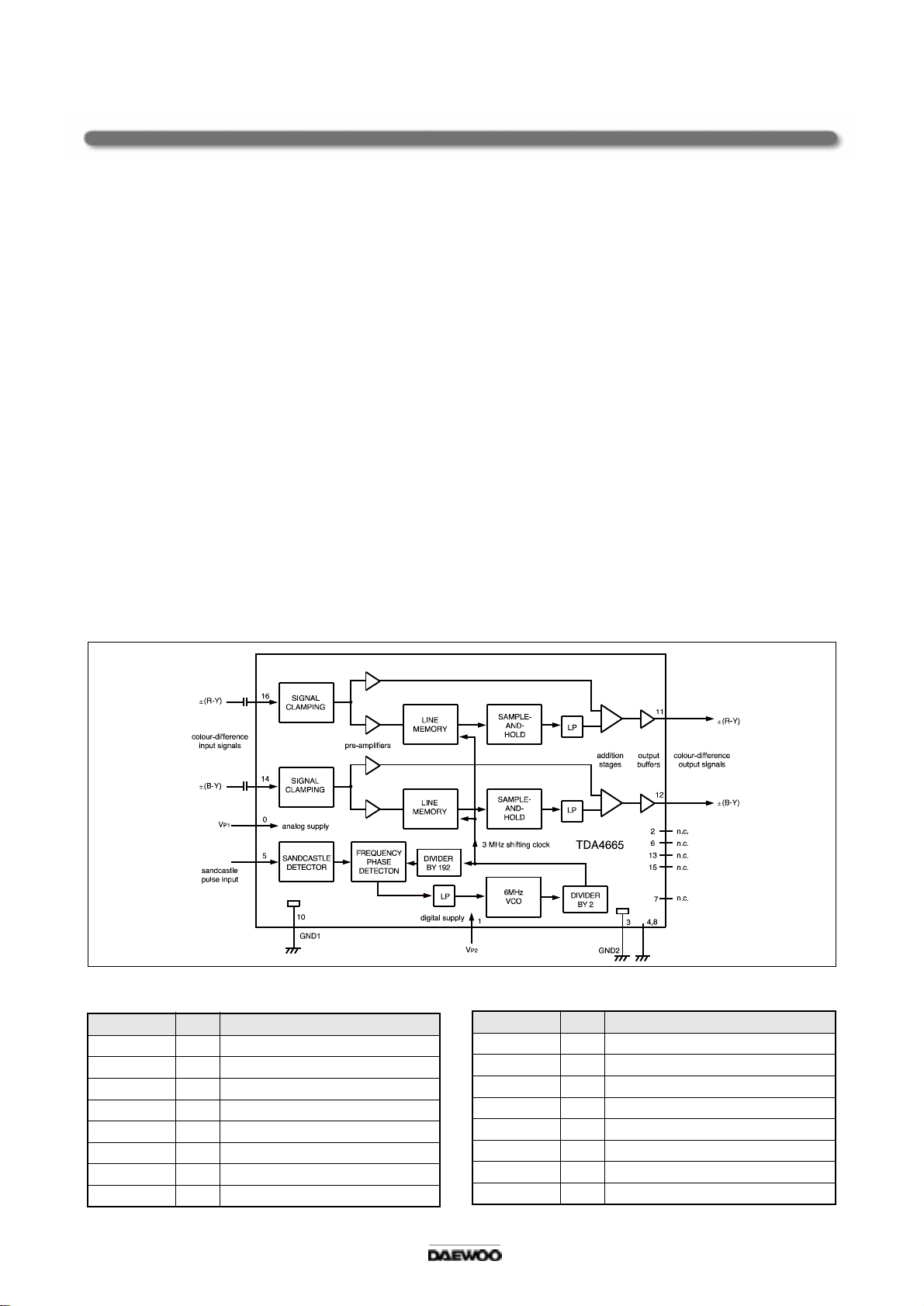
I502 TDA4665(Base Band Delay Line)
1. Features
• Two comb filters, using the switched-capacitor technique,for one line delay tim e (64µ s)
• Adjustment free application
• No crosstalk between S EC AM co lour carriers
• Handles negative or positive colour-difference input signals
• Clamping of A C-coupled input signals(±(R-Y) and ±(B-Y))
• VCO without external components
• 3MHz internal clock signal derived from a 6MH z VCO , line-locked by the sandcastle pulse (64µs line)
• Sample-and -hold circuits and low -pass filters to suppress the 3 M Hz clock signal
• Addition of delayed and non-delayed output signals
• O u tpu t b uffe r a m p lifiers
• Comb filtering functions for N TSC colour-difference signals to suppress cross-colour
2. General Description
The TDA4661 is an integrated baseband delay line circuit w ith one line delay. It is suitable for decoders
with colour-difference signal outputs ± (R-Y) and ± (B-Y).
3. Block Diagram
4. Pin Descriptio n
SYMBOL PIN DESCRIPTION
V
P2
1 +5V supply voltage for digital part
n.c. 2 not connecte d
GN D2 3 ground for digital part (
i.c. 4 internally connected
SAN D 5 sandcastle pulse input
n.c. 6 not connecte d
i.c. 7 internally connected
i.c. 8 internally connected
V)
SYMBOL PIN DESCRIPTIO N
V
P1
9 +5V supply voltage for analog part
GN D1 10 ground for analog part(
(R-Y) 11 ± (R-Y) output signal
V
0
(B-Y) 12 ± (B-Y) output signal
V
0
n.c. 13 not connected
(B -Y ) 1 4 ± (B-Y) inp u t s ign a l
V
1
n.c. 15 not connected
(R -Y) 16 ± (R-Y) inp u t s ign a l
V
1
21
V)
I503 TDA8395 (Secam Decoder)
1. Features
• Fully integrated filters
• A lign m e n t free
• For use with baseband delay
2. Description
The TDA8395 is a self-calibrating,fully integrated SECAM decoder. The IC should preferably be used
in conjunction with the PAL/NTSC decoder TDA8362 and with the switch capacitor baseband delay
circuit TD A4665. The IC incorporates HF and LF filters, a demodulator and an identification circuit
(Ium inance is not processed in this IC).
A highly stable reference frequency is required for calibration and a two-level sandcastle pulse for
blanking and burst gating.
3. Block Diagram
BANDGAP TUNING TUNING
CVBS
16
ACC
INTERFACE
115
f
/IDENT
ref
4. Pin Descriptio n
SYMBOL PIN DESCRIPTION
fp1/IDE NT 1
reference frequency input/identification input
TEST 2 test output
Vp 3 positive supply voltage
n.c. 4 not connecte d
n.c. 5 not connecte d
GN D 6 ground
CLO CH Eref 7 C loche reference filter
PLL ref 8 P LL reference
ref
CLOCHE
100 nF
78362
CLOCHE
FILTER
CONTROL
SAND
220 nF
ref
PLL
PLL
IDENT-
IFICATION
GND
p
V
TDA8395
DE-
EMPHASIS
OUTPUT
STAGE
TEST
10
(R-Y )
9
(B-Y)
SYMBOL PIN DESCRIPTION
-(R -Y) 9 -(R-Y) outp u t
-(B-Y) 10 -(B-Y) output
n.c. 11 not connected
n.c. 12 not connected
n.c. 13 not connected
n.c. 14 not connected
SAN D 15 sandcastle pu lse input
CVB S 16 video(chrominan(e) input)
22
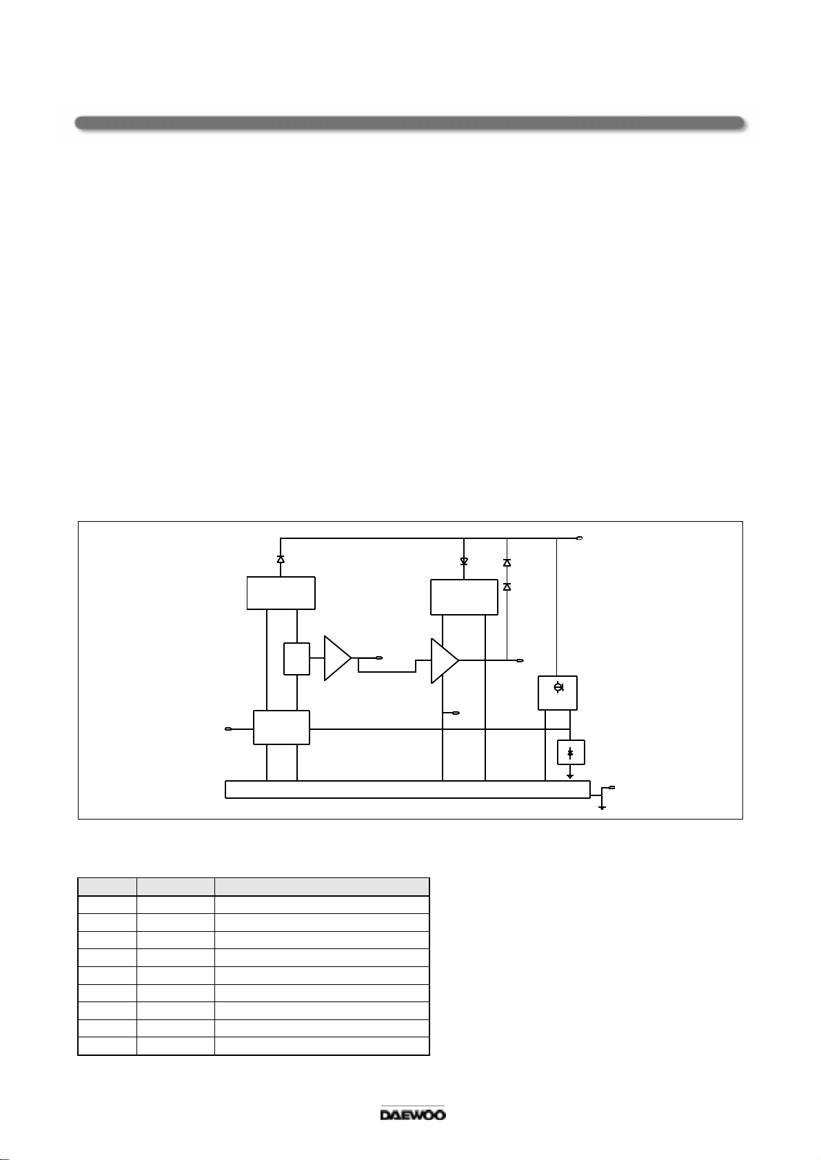
I901, I902, I903 TDA6106Q ( Video Output Amplifier )
1. General Description
The TDA6106Q is a monolithic video output amplifier (5MHz bandwidth) in a SIL 9 MPpackage,
using high-voltage
DM OS technology, and is intended to drive the cathode of CRT directly .
To obtain maximum performance, the amplifier should be used with black-current control.
2. Feature
• Black - current measurement output for autom atic black current stabilization (ABS)
• Single supply voltage of 200V
• Internal protection against positive appearing CRT flash-over discharge
• Protection against E SD
• Inte rn al 2 .5 V refe re n ce circ u it
• Controllable sw itch-off behavior
3. Block Diagram
Pin 6
TDA61O6Q
Vdd
Vdd
MIR R O R 1
in out
MIRROR 3
Pin 9
Vof
Pin 3
vin
1XVbias 1X
DIFF.STAGE
out o u t out o u t
+
4. Pin Descriptio n
PIN SYMBOL DESCRIPTION
1N.C
2N.C
3 V in in v e rting inpu t
4 GND ground, substrate
5 I om B lack-current measurement output
6 V dd supply voltage high
7N.C
8 V oc ca thode output
9 V of feedback/transient output
Vdd
MIR R O R 2
out
Pin5
Ion
in
Pin 8
Voc
CURRENT
SOURCE
gnd
Pin 4
Gnd
in
23
 Loading...