

Daewoo CP-375, 21T2T, 21T2, 20T2T, 20T2 Service Manual
...
Specifications
CRT A34JLL90X01,A34EAC01X06,A34EFU13X01
(OEC) (PHILIPS) (POLKOLOR)
System C14M7E : PAL-B/G for West Europe (Non-TXT)
C14M7F : PAL-B/G, SECAM-L for France (Non-TXT)
C14T7B : PAL- I for U.K (TXT)
C14M7B : PAL- I for U.K (Non-TXT)
C14T7L : PAL - I/I for Ireland (TXT)
C14M7L : PAL - I/I for Ireland (Non-TXT)
Main Voltage 230V AC, 50Hz
Power Consumption Stand-by mode : 8 Watts
Normal operating mode : 39Watts
Sound output 1.5 Watts, 10 % THD at RF 60 % mod.
Speaker 3W 16 ohm x 1 EA
Antenna 75 ohm unbalanced input
Impedance
Tuning system VS( voltage synthesis ) tuning
Tuner 3303KHC (C14M7E, C14M7F, C14T7L, C14M7L)
BAND I : CH2 - CH4
BAND III : CH5 - CH12
CABLE BAND : S1’ - S3’ , S1 - S20
HYPER BAND : S21 - S41
BAND IV, V : CH21 - CH69
DT2-IV17D (C14T7B, C14M7B )
BAND IV, V : CH21 - CH69
Number of 70 programs
program
Aux. Terminal 21 pin EURO-SCART jack
( AV input, TV output, RGB input, S-VHS input )
RCA type AV input jack
Headphone jack (3.5 mm )
Remote controller RM-01A01 with 2 “AA” type batteries
Teletext 8 pages memory TOP & FLOF
(option) : English, German/Dutch/Flemish, French, Italian,
Spanish/Portuguese, Swedish/Finnish/Danish, Czech/Slovak
OSD language -TXT Model : English,French,German,Italian,Spanish
-Non-TXT Model : English,French,German,Italian,Spanish, Russian
1

Safety Instruction
WARNING: Only competent service personnel may carry out work involving the testing or repair of
this equipment.
X-RAY RADIATION PRECAUTION
1. Excessive high voltage can produce potentially
hazardous X-RAY RADIATION.To avoid such
hazards, the high voltage must not exceed the
specified limit. The nominal value of the high
voltage of this receiver is 22-23 at max beam
current. The high voltage must not, under any
circumstances, exceed 27.5 .
Each time a receiver requires servicing, the high
voltage should be checked. It is important to use
an accurate and reliable high voltage meter.
SAFETY PRECAUTION
1. Potentials of high voltage are present when this
receiver is operating. Operation of the receiver
outside the cabinet or with the back board
removed involves a shock hazard from the
receiver.
1) Servicing should not be attempted by anyone
who is not thoroughly familiar with the
precautions necessary when working on highvoltage equipment.
2) Discharge the high potential of the picture tube
before handling the tube. The picture tube is
highly evacuated and if broken, glass
fragments will be violently expelled.
2. The only source of X-RAY Radiation in this TV
receiver is the picture tube.For continued X-RAY
RADIATION protection,the replacement tube
must be exactly the same type tube as specified
in the parts list.
2. If any Fuse in this TV receiver is blown, replace it
with the FUSE specified in the Replacement
Parts List.
3. When replacing a high wattage resistor(oxide
metal film resistor)in circuit board, keep the
resistor 10mm away from circuit board.
4. Keep wires away from high voltage or high
temperature components.
5. This receiver must operate under AC230 volts,
50Hz. NEVER connect to DC supply or any other
power or frequency.
PRODUCT SAFETY NOTICE
Many electrical and mechanical parts in this have
special safety-related characteristics. These
characteristics are often passed unnoticed by a
visual inspection and the X-RAY RADIATION
protection afforded by them cannot necessarily be
obtained by using replacement components rated
for higher voltage,wattage,etc. Replacement parts
which have these special safety characteristics are
identified in this manual and its supplements,
electrical components having such features are
identified by designated symbol on the parts list.
Before replacing any of these components, read the
parts list in this manual carefully. The use of
substitute replacement parts which do not have the
same safety characteristics as specified in the parts
list may create X-RAY Radiation.
3
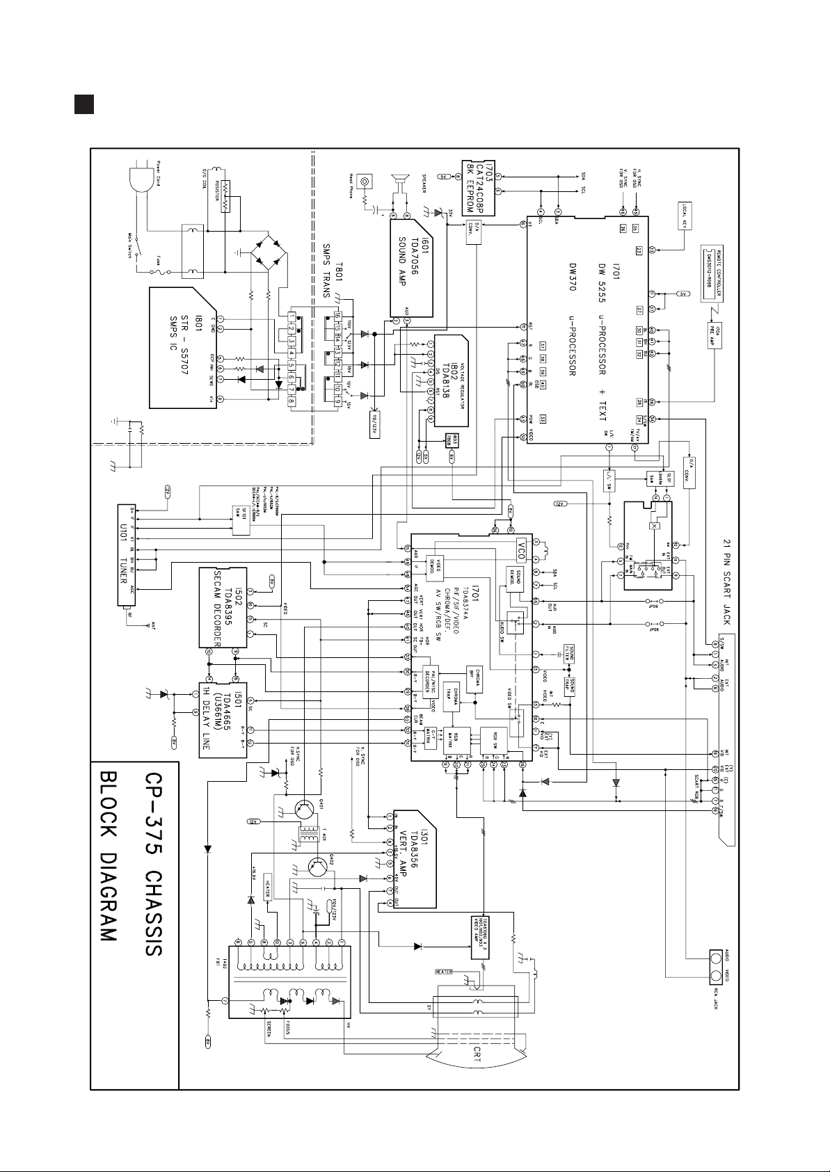
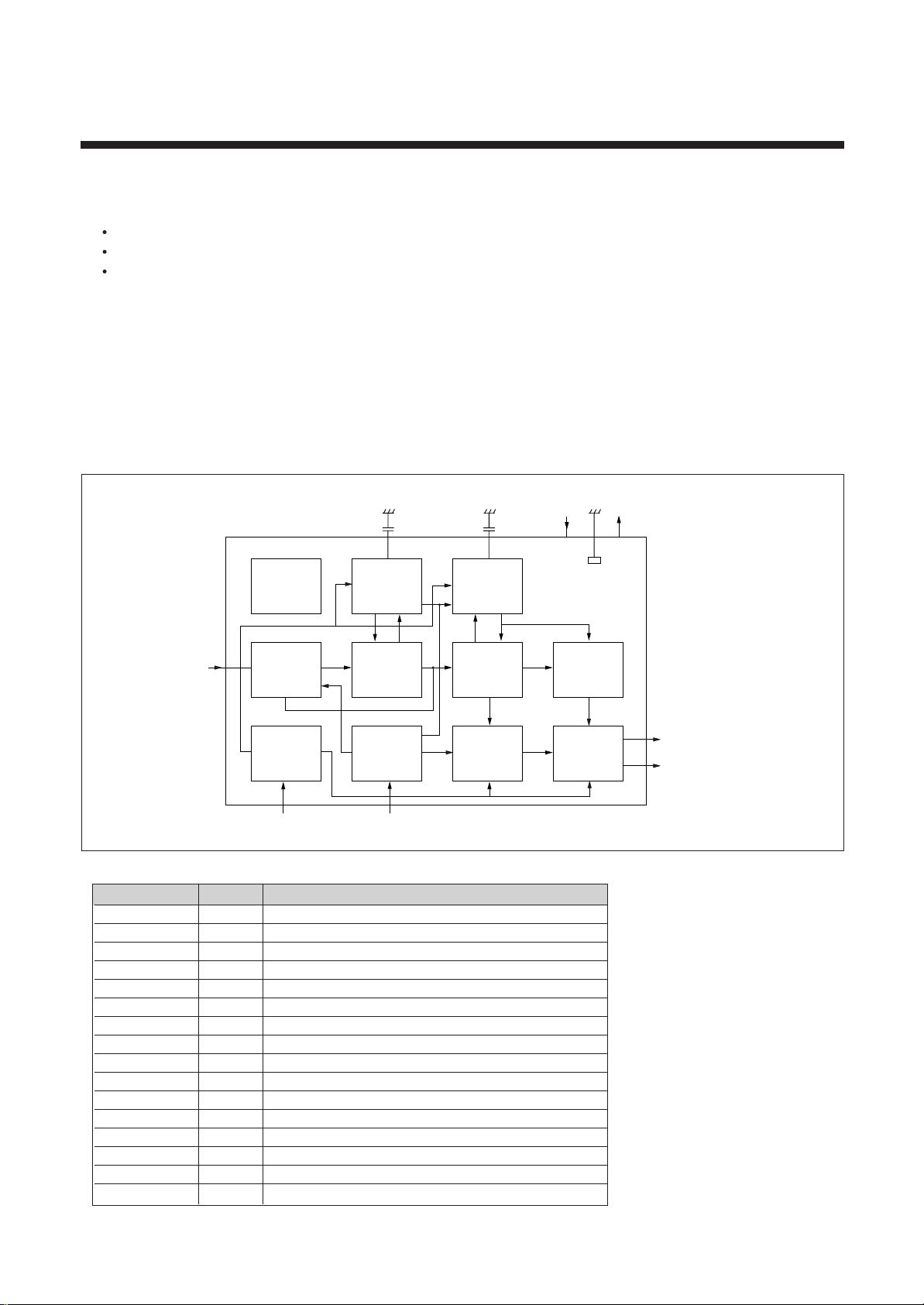
Circuit block Diagram
4
Alignment Instructions
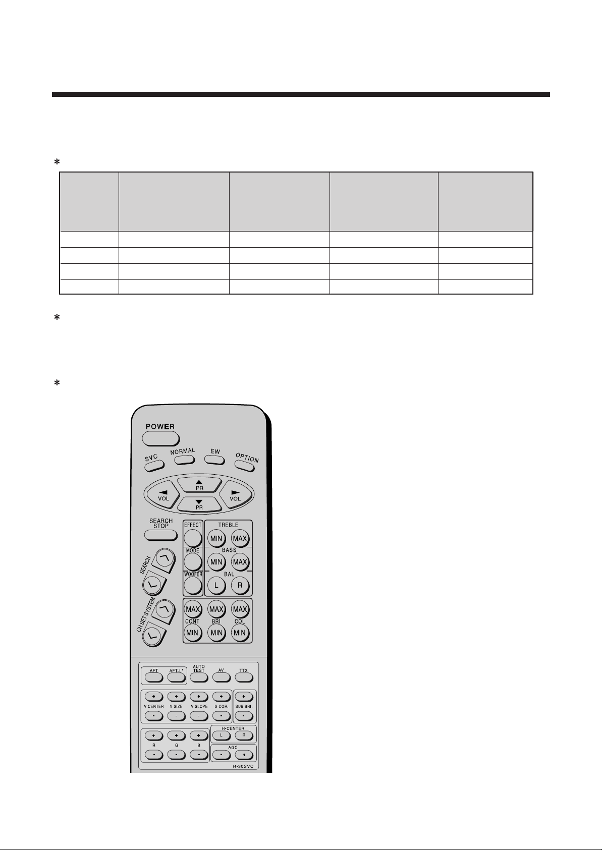
Remark: A service remocon(R-30SVC) is needed to align the set.
1. AFT
1.1 Standard B/G,D/K,I and L
1) Set a Signal Generator with
- RF FREQUENCY = 38.9 MHz,
- RF OUTPUT LEVEL = 80° 5 dBuV
- System = PAL / SECAM - B/G,
2) Connect the Signal Generator RF Output to P101 (Tuner IF Output).
There must be no signal input to the tuner.
3) Press the “AFT” KEY and wait until the TV screen display “AFT OK”.
1.2 Standard SECAM-L’ (France VHF-Low)
Above mentioned “1.1” adjustment has to be done in advance.
1) Set a Signal Generator with
- RF FREQUENCY = 34.2 MHz,
- RF OUTPUT LEVEL = 80° 5 dBuV
- System = SECAM - L’
2) Connect the Signal Generator RF Output to P101 (Tuner IF Output).
There must be no signal input to the tuner.
3) Press the “L’ AFT” KEY and wait until the TV screen display “L AFT OK”.
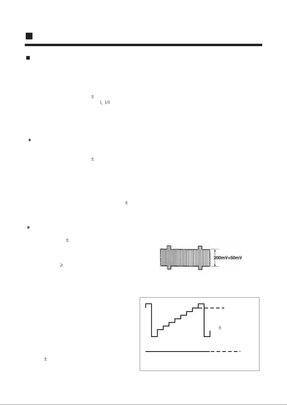
2. AGC
1) Set a Pattern Generator with RF LEVEL 63° 2 dBuV .
2) Connect a OSCILLOSCOPE PROBE to P101 (TUNER AGC INPUT).
3) Adjust AGC UP/DOWN KEY the voltage drop 1V dc over below its maximum voltage.
Alternative Method
1) Set a Pattern Generator with
- RF LEVEL 80° 5 dBuV
- PAL CROSSHATCH
( without SOUND CARRIER )
2) Connect a OSCILLOSCOPE
( Bandwidth 100MHz ) PROBE
to P101 (TUNER IF OUTPUT).
3) Use AGC UP/DOWN KEY to obtain
an envelop amplitude 200 + 50 mVp-p.
3. SCREEN
1) Apply a COLOR BAR pattern signal.
2) Set the CONTRAST, BRIGHTNESS Black level
to MAX, COLOR to MIN.
3) Set the R,G,B LEVEL to CENTER (31/63)
with R,G,B UP/DOWN KEY. 130° 5Vdc
4) Connect a OSCILLOSCOPE PROBE
to P906 ( CRT CATHOD R, G, B ).
5) Adjust the SCREEN VOLUME on FBT
such that the highest black level voltage, GND
130° 5Vdc.
5
4. WHITE BALANCE
1) Set the TV to NOR I mode.
2) Set the R,G,B LEVEL to CENTER with R,G,B UP/DOWN KEY .
3) Adjust the R,G,B UP/DOWN KEY of the other color which did not appear
on the screen to obtain WHITE.
5. FOCUS
1) Apply a RETMA PATTERN signal.
2) Adjust the FOCUS VOLUME on FBT to obtain optimal resolution.
6. GEOMETRY
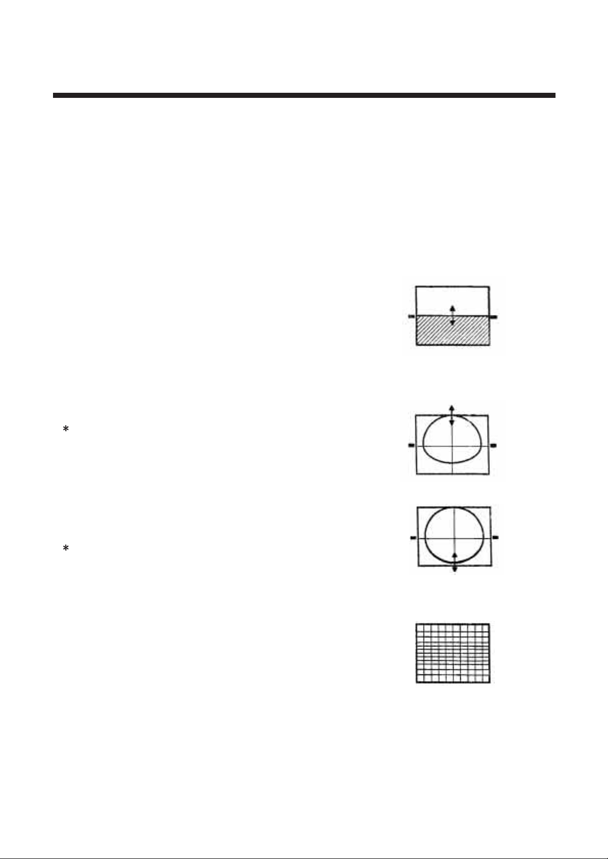
6.1 VERTICAL CENTER
1) Set the TV to NOR I mode.
2) Pressing the V-SIZE UP/DOWN KEY, the
lower half of the screen is blanked.
3) Adjust the border line of blanked picture
coincident with the mechanical center marks
of the CRT using the V-SIZE UP/DOWN KEY.
6.2 VERTICAL SIZE
The VERTICAL CENTER adjustment
has to be done in advance.
1) Apply a RETMA PATTERN signal.
2) Set the TV to NOR I mode.
3) Adjust the upper part of the picture
with the V-SIZE UP/DOWN keys.
6.3 VERTICAL SLOPE
The VERTICAL SIZE adjustment
has to be done in advance.
1) Apply a RETMA PATTERN signal.
2) Adjust the lower part of the picture
with the V-SLOPE UP/DOWN keys.
6.4 VERTICAL S-CORRECTION
1) Apply a CROSSHATCH PATTERN signal.
2) Adjust the S-COR UP/DOWN KEY to obtain
the same distance between horizontal lines.
6.5 HORIZONTAL CENTER
1) Apply a RETMA PATTERN signal.
2) Adjust picture centering with CENTER
LEFT/RIGHT keys.
6
If EEPROM (I703) has been changed ;
- Option data has to be changed and
- all alignment function has to be readjusted .
Option
Initial state C14M7F C14T7B C14M7E
C14M7B C14T7L
C14M7L
(Blank EEPROM) (FRANCE) ( U.K ) (OTHERS)
AV AV2 AV2 AV2 AV2
BAND 3 BAND 3 BAND 1 BAND 3 BAND
FRANCE OFF ON OFF OFF
ATS ON ON ON ON
The initial state of adjustment are as follows;
- V-Center, V-Slope V-Size, H-Center, R, G, B, AFT = Center ( 30/64 - 33/64 )
- S-Correction = 00/64
- AGC = 10/64
Service Remocon
7

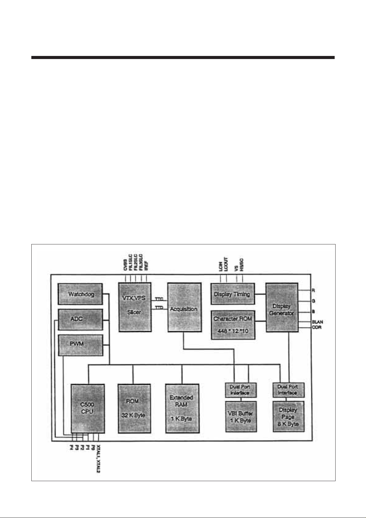
IC Description
DW5255M*(Micro-controller & West/East Teletext Decoder)
DW5255RM*(Micro-controller & Cyrillic Teletext Decoder)
=SDA5255-A*** (SIEMENS Type No.)
(1) General Description
The TDA5255 contains a slicer for VPS and TTX, an accelerating acquisition hardware module, a display
generator for “LEVEL 1” TTX data and a 8 bit u-controller running at 333 nsec cycle time.
The controller with dedicated hardware guarantees flexibility, does most of the internal processing of TTX
acquisition , transfers data to/from the external memory interface and receives/transmits data via I2C and
UART user interfaces.
The Slicer combined with dedicated hardware stores TTX data in a VBI 1Kbyte buffer.
The u-controller firmware does the total acquisition task ( hamming- and parity -checks,
page search and evaluation of header control bits) once per field.
(2) Feature
•
Acquisition:
- feature selection via special function register
- simultaneous reception of TTX and VPS
- fixed framing code for VPS and TTX
- programmable framing code window for TTX
- Acquisition during VBI
- direct access to VBI RAM buffer
- Acquisition of packets x/26, x/27, 8/30 (firmware)
- assistance of all relevant checks (firmware)
- 1-bit framing-code error tolerance (switchable)
•
. Display:
- features selectable via special function register
- 50/60 Hz display
- level 1 serial attribute display pages
- blanking and contrast reduction output
- 8 direct addressable display pages
- 12 x 10 character matrix
- 96 character ROM (standard G0 character set)
- 143 national option characters for 11 languages
- 288 characters for X/26 display
- 64 block mosaic graphic characters
- 32 free addressable characters for OSD in expanded character ROM + 32 inside OSD box
- double height (TOP/BOTTOM)
- conceal/reveal
- transparent foreground/background -inside/outside of a box
- cursor (colour changes from foreground to background colour)
- flash (flash rate 1s)
- programmable horizontal und vertical sync delay
- hardware assisted fast display page erase
- full screen background colour in outer screen
•
Synchronization:
display synchronization to sandcastle or Horizontal Sync (HS) and Vertical Sync (VS) with startstop-oscillator or
display synchronization to sandcastle or Horizontal Sync and Vertical Sync with external clock
independent clock systems for acquisition, display and controller
8
•
Controller:
- 8 bit configuration
- 18 MHz internal clock
- 0.33 us instruction cycle
- eight 16-bit data pointer registers (DPTR)
- two 16-bit timers
- watchdog timer
- serial interface (UART)
- 256 bytes on-chip RAM
- 1 Kbyte on-chip extended RAM (access via MOVX)
- 8 Kbyte on-chip ACQ-buffer-RAM (access via MOVX)
- 6 channel 8-bit pulse width modulation unit
- 2 channel 14-bit pulse width modulation unit
- 4 multiplexed ADC inputs with 8-bit resolution
- one 8-bit I/O port with open drain output and optional I2C emulation
- two 8-bit multifunctional I/O ports
- one 4-bit port working as digital or analog inputs
- one 2-bit I/O port with optional address latch enable function
•
P-SDIP 52 package
•
5 V supply voltage
(3) Block Diagram
9

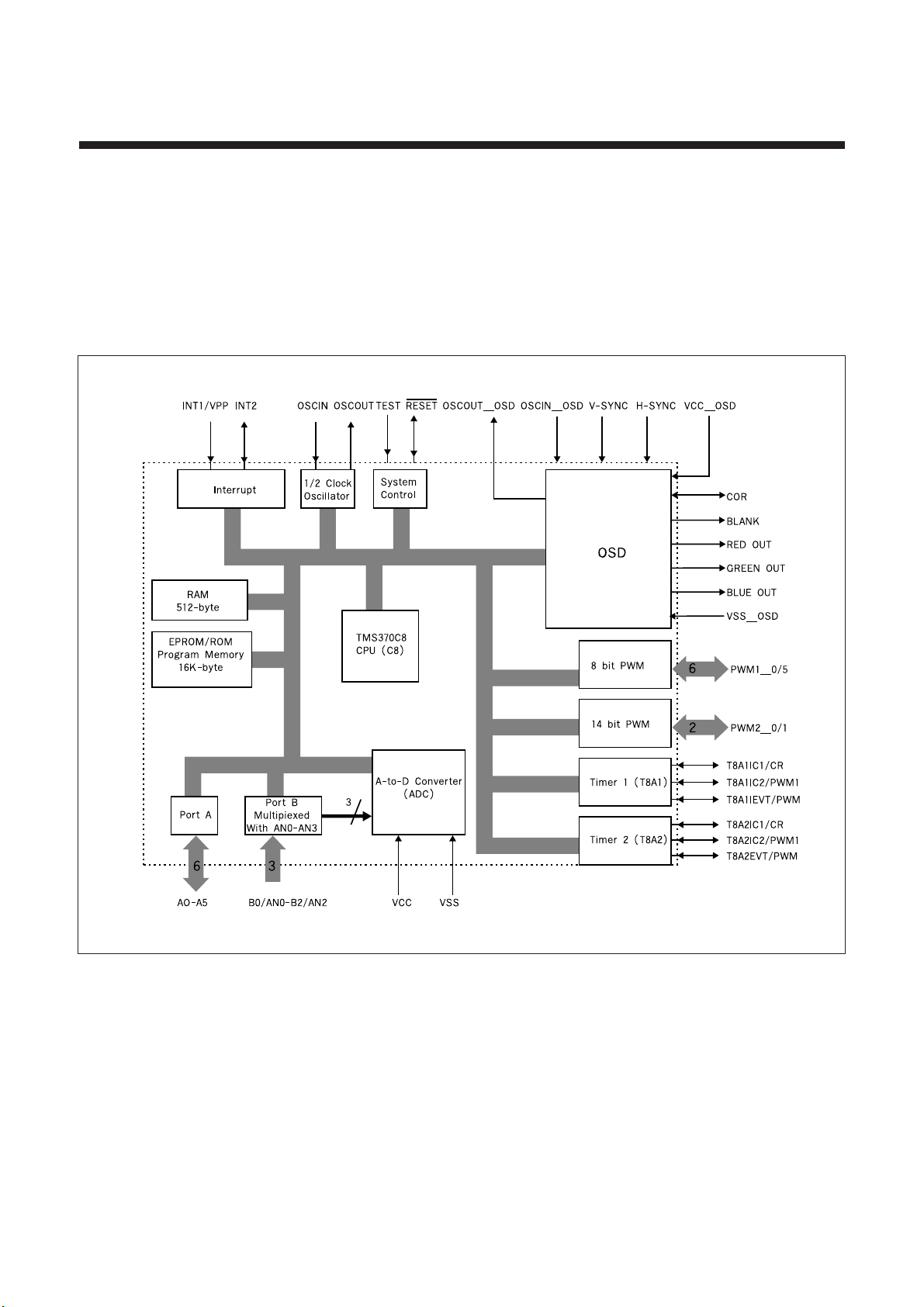
DW370M* (Micro-controller for Non-Teletext Model)
=TMS370C08A05 ( TI Type No.)
=TMS370P08A05 (OTP device)
(1) General Description
The TMS370C08A05 devices are members of the cMCU370 family single-chip microcontrollers.
The cMCU370 family provides cost effective real-time system control through use of the PRISM methodology.
The PRISM methodology modular fabrication process integrates analog, digital, linear and power technologies on a
single chip, thereby maximizing the total integration strategy.
The TMS370C08A05 devices are designed with the high-performance 8-bit TMS370C8 CPU.
Features of the ‘C8 CPU and system module as implemented on this device include three CPU registers (stack
pointer, status register, and the program counter), two external interrupts, reset, memory mapped control registers.
(2) Feature
•
Internal Memory Configurations
- 16K-Byte ROM Program Memory
- 512-Byte RAM
•
Operating Features
- Supply Voltage (VCC) 5 V ° 10%
- Input Clock Frequency 2, 20MHz
- Industrial Temperature Range
•
Device Integrity Features
- Address Out-of-Range Reset
- Stack Overflow Reset
- Parallel Signature Analysis (CRC)
•
Two 16-Bit General Purpose Timer(T8A)
Each Includes:
- 16-Bit Resettable Counters with individual 8-Bit Prescaler
- 2 PWM Channels or
- 2 Input Captures or
- 1 Input Capture and 1 PWM Channel
•
One 14-Bit PWM Module
- 14-Bit Resettable Counters
- 14-Bit PWM Output Port
•
One 8-Bit PWM Module
- 8-Bit Resettable Counters
- 8-Bit PWM Output Port with 12V Open Drain
•
OSD Module
- Blanking/ Contrast reduction out
- Transparent Background
- Transparent Foreground
- Full Screen Background Color
- Controlled Color, Blink, Size, Smoothing, Fringe of Each lines of Character
- Two size of different Font 12x10 and 12x18 by Hard Masking
- OSD Window Display with 40x25 lines
•
8-Bit A/D Converter With 3 Inputs
- Single or Dual Channel Operation
- Single or Continuous Conversion Modes
•
Flexible Interrupt Handling
- Global and Individual Interrupt Masking
10
- 2 S/W Programmable Interrupt Levels
- 2 External Interrupt (1 Non-Maskable)
- Programmable Rising or Falling Edge Detect
•
09 CMOS Compatible I/O Pins
- All Peripheral Function Pins Software Configurable for Digital I/O
- 6 Bidirectionals, 3 Input Pins
•
Plastic 42 YSDP Pins Package
(3) Block Diagram
11
(4) Pin Description
* A : DW5255M*/DW5255RM*, B : DW370M*
Pin Name Symbol Description
A* B* A* B
1 1 P3.1 T1IC1/CR SYS SECAM-L’ OUT for switching SAW filter
L9461
- SECAM-L’ : H
- SECAM- L : L
2 2 P0.7/Open Drain A0 BUSSTOP I2C BUS STOP IN for Computer
controlled alignment in Factory
( Active Low )
3 3 P0.6/Open Drain A1 SDA Serial data IN/OUT for I2C
4 4 P0.5/Open Drain A2 SCL Serial clock IN/OUT for I2C
5 5 P0.4/Open Drain A3 OPTION #5 #6 Teletext
6 6 P0.3/Open Drain A4 OPTION H H West Teletext
L H East Teletext
H L Turkish Teletext
7 7 P0.2/Open Drain A5 OPTION Auto search priority
H : L/L’ priority
L : B/G priority
8 8 P0.1/Open Drain PWM1-0/ Open Drain OPTION Not Used (Reserved)
9 9 P0.0/Open Drain PWM1-1/ Open Drain LED LED drive OUT
- Stand-by mode : H
- Operating mode : L
( IR reception : pulse )
10 10 VSS VSS ground
11 11 VCC VCC Power Supply
12 12 XTAL1 OSCIN OSCIN Input to inverting osc. Amplifier
13 13 XTAL2 OSCOUT OSCOUT Output of inverting osc. Amplifier
14 14 P4.0/ALE PWM1-2/Open Drain Not Used
15 15 RESET RESET/Open Drain RST RESET IN (ACTIVE LOW)
16 16 P1.7/14BIT PWM PWM2-0 VT TUNING VOLTAGE OUT
17 17 P1.6/14BIT PWM PWM2-1 SW TV/AV &AM/FM SW.OUT for
STV8225
18 18 P1.5/8BIT PWM PWM1-3/Open Drain F/SW F/SW IDENT IN for stopping OSD
display in RGB mode
- H : TV /AV mode
- L : RGB mode
19 19 P1.4/8BIT PWM PWM1-4/Open Drain Not Used
20 20 P1.3/8BIT PWM PWM1-5/Open Drain MUTE AUDIO MUTE OUT
21 21 P1.2/8BIT PWM TEST GND (Must be tied 0V for DW370M*)
22 P1.1/8BIT PWM Not Used
23 P1.0/8BIT PWM Not Used
24 VSSA VSSA Analog GND for Slicer
25 FIL3 FIL3 PLL Loop Filter I/O for Phase Shifting
12
Pin Name Symbol Description
A* B* A* B
26 FIL2 FIL2 PLL Loop Filter I/O for TTX Slicing
27 FIL1 FIL1 PLL Loop Filter I/O for VPS Slicing
28 VCCA VCCA Analog Supply for Slicer
29 IREF IREF Reference Current for Slicer PLLs
30 CVBS CVBS CVBS IN
31 P2.3/8 bit ADC Not Used
32 22 P2.2/8 bit ADC B0/AN0/ADC AGC IF AGC INPUT for Auto Tuning System
33 23 P2.1/8 bit ADC B1/AN1/ADC KS Local KEY SCAN IN
34 24 P2.0/8 bit ADC B2/AN2/ADC S/SW S/SW IDENT IN for Automatic
switching between TV/AV mode
- H : AV / RGB mode
- L : TV mode
35 25 VSS VSS-OSD VSS Ground
36 26 P3.3/INT1 INT1 IR REMOTE IR IN
37 27 VDD VCC-OSD VDD Power Supply
38 28 LCIN OSCIN-OSD LCIN CLOCK IN for OSD
39 29 LCOUT OSCOUT-OSD LCOUT CLOCK OUT for OSD
40 30 P3.7/TXT I/O T2EVT/PWM2 BL BAND VHF-L OUT ( Active High )
41 31 P3.6/RXD T2IC2/PWM1 BH BAND VHF-H OUT ( Active High )
42 32 P3.5/T1 T2IC1/CR BU BAND UHF OUT ( Active High )
43 33 P3.4/T0 T1EVT/PWM2 POWER POWER CONTROL OUT
44 34 P3.2/INT0 INT2 Not Used
45 35 HS/SC HSYNC HSYNC HOR. SYNC. IN (Active High)
46 36 P4.7/VS VSYNC VSYNC VERT. SYNC. IN (Active High)
47 37 R R RED OUT
48 38 G G GREEN OUT
49 39 B B BLUE OUT
50 40 BLANK BL BLANK OUT
51 41 COR COR Not Used
(CONTRAST REDUCTION OUT)
52 42 P3.0 T1C2/PWM1 EVEN/ODD EVEN/ODD OUT for non-interlacing
in TTX mode
13
CAT24C08P (E2PROM)
Vcc
Vgg
SDA
TEST
SEL
A0
A1
A2
D OUT
AKC
SENSE AMPS
SHIFT REGISTERS
WORD ADDRESS
BUFFERS
COLUMN
DECODERS
XDEC
64
2
START/STOP
LOGIC
CONTROL
LOGIC
DATE IN STORAGE
HIGH VOLTAGE/
TIMING CONTROL
STATE COUNTERS
SLAVE
ADDRESS
COMPARATORS
EXTERNAL
(1) Typical Features
•
IC Bus compatible
•
Low power CMOS Technology
•
16 Byte page write Buffer
•
Self-Timed Write cycle with Auto-Clear
•
100,000 program/Erase cycles
•
100 Year Data Retention
•
Optional High Endurance Device Available
(2) Description
The CAT24C08P is a 8K bit serial CMOS E2PROM internally organized as 1024x8bits.
The CAT 24C08P features a 16 byte page write
buffer.
(3) Block Diagram
(4) Pin Description
PIN SYMBOL DESCRIPTION
1-3 A0, A1, A2 Device Address lnputs
4 Vss Ground
5 SDA Serial Data/Address
6 SCL Serial Clock
7 TEST Connect to Vss
8 Vcc +5V Power supply
14

TDA8374A (Single chip TV Processor for Negative modulation IF )
TDA8374 (Single chip TV Processor for Negative & positive modulation IF)
(1) General Description
The TDA8374(A) is I2C-bus controlled single chip TV processors which are intended to be applied in PAL/NTSC
television receiver.
The IC is mounted in a S-DIL 56 envelope.
(2) Feature
•
IF
- Vision IF amplifier with high sensitivity and good figures for differential phase and gain
- PLL demodulator with high linearity offering the possibility for (single standard) intercarrier stereo audio application .
- Alignment PLL via I2C
- [TDA8374] Multistandard IF with negative and positive modulation, switchable via I2C
•
AUDIO
- Alignment free multi standard PLL audio demodulator (4.5 to 6.5 MHz.)
- Mono volume control
•
Video
- Integrated luminance delay line
- Integrated chroma trap and bandpass filters (auto calibrated)
- Asymmetrical peaking circuit in the luminance channel
- Black stretching of non standard CVBS or luminance signals
•
Colour
- SECAM interface for application with SECAM add-on TDA8395.
•
RGB
- RGB control (brightness, contrast, saturation)
- Black current stabilization and white point adjustment
•
Input / Output
- Flexible video source select with CVBS input for the internal signal and two external video inputs(one switchable for
CVBS or Y/C).
- The output signal of the video source select is externally available ( also as CVBS when Y/C input is used).
- External audio input.
- Linear RGB input with fast blanking.
•
Synchronization and Deflection
- Horizontal synchronization with two control loops and alignment free horizontal oscillator.
- Slow start and slow stop of the horizontal drive output to enable low stress start-up and switch-off from the line circuit
at nominal line supply voltage.
- Vertical count-down circuit for stable behavior with provisions for non-standard signals.
- Vertical geometry control.
- Vertical drive optimized for DC coupled vertical output stages.
•
Control
- Full I2C bus control, as well for customer controls as for factory alignment.
- All automatic controls have an option for forced mode.
•
Power consumption
- Low power consumption (900 mW at 8.0 Volts).
•
Packaging
- SDIL-56 (Shrinked Dual In Line, 56 pins).
15
(3) Block Diagram
16
(4) Pin Description
No Name Description
1 SOUND IF INPUT The sound equivalent input impedance is 8k5 ohm // 5pF which has to be
taken into account for proper termination of the ceramic filters.
The DC impedance is very high.
The minimum input signal for catching is l mV rms.
2 EXT AUDIO INPUT An external sound signal (500mVrms) for example from SCART can be
applied to this pin via a coupling capacitor.
The input impedance is 25kohm.
3 VCO REF FILTER The IF VCO tuned circuit is applied to these pin.
4 Its resonance frequency must be two times the IF-frequency and in between a
range of 64-120MHz.
This range is suitable for the IF standards as 33.4, 38.9, 45.75 and 58.75MHz.
The VCO frequency can be adjusted by I2C bus so a fixed coil can be used.
5 PLL LOOP FILTER The PLL loopfilter is a first order filter with R=390 ohm and C = 100nF in
series to ground.
The loopfilter bandwidth is 60kHz and is optimal for both fast catching and
sufficient video suppression for optimal sound performance.
Sound performance can theoretically be improved by adding a small
capacitor (approx.0- 4.7nF) between pin 5 and ground.
This however must be evaluated further because the normal video signal
response should not be effected.
6 IF VIDEO OUTPUT Although the video output impedance is low it is recommended to avoid
high frequency current in the output due to for instance sound trap filters.
This can be achieved by means of an emitter follower at the video output with
a 1 resistor in series with the base.
7 BUS INPUT : SCL Serial clock line
8 BUS INPUT : SDA Serial data line
9 BANDGAP The bandgap circuit provides a very stable and temperature independent
DECOUPLING reference voltage.
This reference voltage (6.7V) ensures optimal performance of the TDA8374
and is used in almost all functional circuit blocks.
10 CHROMA INPUT The supplied C S-VHS input burst amplitude should be nominally 300mVpp
(assumed is a colour bar signal with 75% saturation and with chroma/burst
ratio of 2.2/1 ). The C S-VHS input is internally clamped to 4V via 50 .
The external AC coupling capacitor with 50 forms a high pass filter.
A recommended coupling capacitor is 1 nF; the high pass filter cut off
frequency is then approximately 3KHz.
11 Y/CVBS INPUT The Y S-VHS signal of 1Vpp ( inclusive sync amplitude) is AC coupled to pin11.
12 MAIN The TDA8374 has a main supply pin 12 and a horizontal supply pin 37. Both
37 POSITIVE SUPPLY pins have to be supplied simultaneously.
Notice that the IC has not been designed to use this pin 37 as start pin.
(pin 37 supplies the horizontal oscillator, PHI-1 and PHl-2)
(pin 12 supplies the rest of the circuits in the IC)
The nominal supply voltage is 8V. With min/max values of 7.2-8.8V.
Also in stand-by condition the IC must be supplied with 8V.
17
No Name Description
A voltage detection circuit is connected to both pins.
- pin12 if V12 <6.8V than a power on reset, POR, is generated. The Hout
output is disabled immediate.
- pin37 if V37 <5.8V than the horizontal output is disabled immediate.
13 INT CVBS INPUT It is recommended that the CVBS1 int and CVBS2 ext input amplitudes are
17 EXT CVBS INPUT 1 Vpp (inclusive sync amplitude).
This, because the noise detector switches the 1 loop to slow mode
(i.e. auto 1mode when FOA, FOB = 0,0) when noise level exceeds
100mVrms (i.e. at S/N of 20dB).
14 GROUND All internal circuits are connected to this ground pin 14.
15 AUDIO OUTPUT The output signal is volume controlled and is active for both internal and
external audio signals. The nominal gain is +9dB and -71dB, which gives
a total control range of 80dB.
The output signal range therefor is 0.14- 1400mVrms
The bandwidth is >100kHz, the DC level is 3.3V and the output impedance
is 250 .
16 DECOUPLING Voltage variations at pin 16, which can be due to external leakage current or
FILTER TUNING crosstalk from interference sources, should be less than 50mV to ensure that
tuning of filters/delay cells remains correct.
18 BLACK CURRENT For correct operation of the loop CURRENT information is supplied to the
INPUT black current input pin.
19 BLUE OUTPUT The RGB outputs are supplied to the video output stages from pins 21, 20
20 GREEN OUTPUT and 19 respectively.
21 RED OUTPUT For nominal signals (i.e. CVBS/S-VHS, -(R-Y)/- (R-Y), TXT inputs) and for
nominal control settings, then the RGB output Signal amplitudes is
typically 2VBLACK_WHITE.
22 V-GUARD INPUT/ Vertical Guard
BEAM CURRENT With this function, the correct working of the vertical deflection can be
LIMITER monitored. If the vertical deflection fails, the RGB outputs are blanked to
prevent damage to the picture tube.
Beam current limitinq
The beam current limiting function is realised by reducing the contrast (and
finally the brightness) when the beam current reaches s too high level. The
circuit falls apart in two functions:
- Average beam current limiting (ABL): reacting on the average content of
the picture
- Peak white limiting (PWL): reacting on high local peaks in the RGB signal.
23 RED INPUT The Rin, Gin, Bin input signals (nominal signal amplitude of 700mV) are
24 GREEN INPUT AC coupled to pin 23, 24 and 25 respectively.
25 BLUE INPUT Clamping action occurs during burstkey period.
26 RGB INSERTION The table below a survey is given of the three modes which can be selected
SWITCH INPUT with a voltage on RGB insertion switch input pin ;
Vpin26 I2C function Selected RGB signal
0.9V-3V IE1=0 RGB(internal)
IE1=1 Rin,Gin,Bin
(fast insertion on pin23,24,25)
> 4V IE1=X OSD can be inserted at the RGBout pins
27 LUMINANCE INPUT An nominal input signal amplitude of 1 Vblack-white MUST be DC coupled
18

No Name Description
to the luminance input pin 27.
The pin is internally AC coupled to the luminance clamp via a capacitor of
50pF; clamping action occurs during burstkey period.
28 LUMINANCE The luminance output signal is approximately l V black-white with typical
OUTPUT output impedance of 25O ohm.
29 B-Y OUTPUT The maximum output impedance of pins 29 and 30 is 500 when PAL/NTSC
30 R-Y OUTPUT signals are identified. When SECAM is identified by the SECAM add-on and
no PAL/NTSC is already identified by the ASM, then the ASM sets the
-(B-Y)/-(R-Y) output switch open (via DEMSW).
This enables the -(B-Y)/-(R-Y) outputs of the TDA8395 to be directly connected
to pins 29 and 3O respectively.
31 B-Y INPUT The -(B-Y),-(R-Y) output signals (supplied from baseband delay line) are AC
32 R-Y INPUT coupled, via a coupling capacitor of 10nF or greater, to the -(B-Y)/-(R-Y) inputs;
both inputs are clamped during burstkey period.
33 SECAM REF The SECAM reference output is directly connected to pin l of the TDA8395 for
OUTPUT SECAM decoding ; it also can be used as a reference for comb filter applications.
34 X-TAL 3.58 To ensure correct operation of both:
35 X-TAL 4.43 - colour processing internal circuits,
- sync calibration internal circuits,
it is only allowed to have 3.6MHz Xtals on pin34: both 4.4MHz,3.6MHz Xtals
are allowed on pin 35.
If pin 35 is not used: then it is left open in application (also XA,XB=O,1 ).
36 LOOP FILTER One of the important aspects of the PLL is the 1oop filter connected to pin 36;
BURST PHASE it influences the dynamic performance of the loop.
DETECTOR
38 CVBS OUTPUT The output amplitude is 1Vpp (transfer gain ratio between CVBS1int or
CVBS2ext or CVBS3ext/Ys-vhs and CVBSout is 1).
The maximum output impedance is 250 ohm.
39 BLACK PEAK For the correct working of the black stretcher an external time constant should
HOLD CAPACITOR be added at the black peak hold capacitor input.
40 HOR OUTPUT This open collector output is meant to drive the horizontal output stage.
The output is active low, i.e. the line transistor should conduct during the low
period of the output.
41 SANDCASTLE Pin 41 is a combined input/output pin.
OUTPUT/ The pin provides a three level sandcastle pulse.
FLYBACK INPUT Both burstkey pulse and vertical blanking pulse are always available, the line
blanking pulse is only present when the external flyback pulse is fed to this pin.
The line flyback pulse, fed to this pin is used for two functions:
- input signal for the PHI-2 1oop and
- RGB line blanking. (without flyback pulse blanking occurs only during the
burstkey pulse)
To ensure correct working of the delay line and SECAM add-on, the output
should not be loaded with more than:
- Sandcastle input delay line TDA 4665
- Sandcastle input SECAM add-on TDA 8395
42 PHI-2 FILTER / The loopfilter is a first order filter.
FLASH PROTECT This pin requires a capacitor (C) only.
19
No Name Description
A flash protection becomes active when this pin is forced >6V. The horizontal
drive is switched-off immediately.
Once the voltage is <6V the horizontal drive is switched-on again via the slow
start procedure.
43 PHI-1 FILTER The loopfilter connected to pin 43 is suitable for various signal conditions as
strong/weak and VCR signal.
This is achieved by switching of the loopfilter time constant by changing the
PHI-1 output current.
Via I2C bus FOA/B, different time constants can be chosen, including an
automatic mode which gives optimal performance under varying conditions.
44 GROUND To this pin are connected the IC-substrate and horizontal output.
45 EAST-WEST DRIVE not used
46 VERT DRIVE + The vertical drive has a current output. The output is balanced which ensures
47 VERT DRIVE - a good common mode behavior with temperature and makes the output signal
less sensitive for disturbances.
48 IF INPUT The PLL frequency range is 32-60MHz with corresponding VCO frequency
49 64-120MHz.
The IF input impedances is 2 in parallel with 3pF and matches the required
load for commonly used SAW filters.
A DC coupling is allowed, so no series capacitors between SAW filter and IF
input are necessary.
50 EHT/OVERVOLTAGE not used
PROTECT INPUT
51 VERT This pin requires a capacitor to ground of l00nF +,- 5%.
SAWTOOTH The optimal sawtooth amplitude is 3.5V and is determined by the external
CAPACITOR capacitor and charge current.
The sawtooth bottom-level is 2V.
52 REFERENCE This pin requires a resistor to ground.
CURRENT INPUT The optimal reference current is 100 . which is determined by this resistor.
53 AGC The AGC capacitor value is 2.2 and has been defined for an optimal
DECOUPLING compromise between AGC speed and tilt for all AGC modes
CAPACITOR (negative/positive modulation).
54 TUNER AGC This output is used to control (reduce) the tuner gain for strong RF signals.
OUTPUT The tuner AGC is an open collector output which is acting as a variable
current source to ground.
55 AUDIO Only a capacitor has to be connected to this pin that defines the deemphasis
DEEMPHASSIS time constant.
The signal is internally connected through to the Audio switch.
The deemphasis output is fixed, thus not controlled by the volume, and can be
used for SCART.
56 DECOUPLING This pin requires a capacitor of 10 connected to ground.
SOUND The pin acts as a low pass filter needed for the DC feedback loop.
DEMODULATOR
20
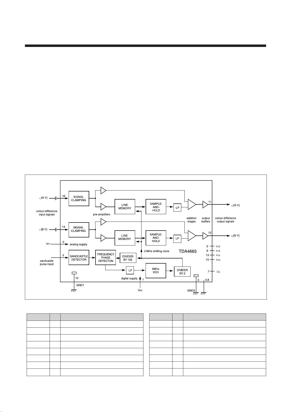
TDA4665(Base Band Delay Line)
(1) Features
• Two comb filters, using the switched-capacitor technique,for one line delay time (64µs)
• Adjustment free application
• No crosstalk between SECAM colour carriers
• Handles negative or positive colour-difference input signals
• Clamping of AC-coupled input signals(±(R-Y)and±(B-Y))
• VCO without external components
• 3MHz internal clock signal derived from a 6MHz VCO, line-locked by the sandcastle pulse (64µs line)
• Sample-and -hold circuits and low-pass filters to suppress the 3 MHz clock signal
• Addition of delayed and non-delayed output signals
• Output buffer amplifiers
• Comb filtering functions for NTSC colour-difference signals to suppress cross-colour
(2) General Description
The TDA4661 is an integrated baseband delay line circuit with one line delay. It is suitable for decoders
with colour-difference signal outputs±(R-Y)and±(B-Y).
(3)Block Diagram
(4) Pin Description
SYMBOL PIN DESCRIPTION
Vp2 1 +5V supply voltage for digital part
n.c. 2 not connected
GND2 3 ground for digital part (0V)
i.c. 4 internally connected
SAND 5 sandcastle pulse input
n.c. 6 not connected
i.c. 7 internally connected
i.c. 8 internally connected
SYMBOL PIN DESCRIPTION
Vp1 9 +5V supply voltage for analog part
GND1 10 ground for analog part (0V)
V0 (R-Y) 11 ±(R-Y) output signal
V0 (B-Y) 12 ± (B-Y) output signal
n.c. 13 not connected
V1 (B-Y) 14 ± (B-Y) input signal
n.c. 15 not connected
1 (R-Y) 16 ±(R-Y) input signal
V
21
TDA8395 (Secam Decoder)
(1) Features
Fully integrated filters
Alignment free
For use with baseband delay
(2) Description
The TDA8395 is a self-calibrating,fully integrated SECAM decoder. The IC should preferably be used
in conjunction with the PAL/NTSC decoder TDA8362 and with the switch capacitor baseband delay
circuit TDA4665. The IC incorporates HF and LF filters, a demodulator and an identification circuit
(Iuminance is not processed in this IC).
A highly stable reference frequency is required for calibration and a two-level sandcastle pulse for
blanking and burst gating.
(3) Block Diagram
ref PLLref GND
CLOCHE
100 nF
78362
220 nF
TEST
V
p
BANDGAP TUNING TUNING
CVBS
16
ACC
INTERFACE
115
ref/IDENT
f
CLOCHE
FILTER
CONTROL
SAND
PLL
IDENT-
IFICATION
(4) Pin Description
SYMBOL PIN DESCRIPTION
fp1/IDENT 1 reference frequency input/identification input
TEST 2 test output
Vp 3 positive supply voltage
n.c. 4 not connected
n.c. 5 not connected
GND 6 ground
CLOCHEref 7 Cloche reference filter
PLL ref 8 PLL reference
-(R-Y) 9 -(R-Y) output
-(B-Y) 10 -(B-Y) output
n.c. 11 not connected
n.c. 12 not connected
n.c. 13 not connected
n.c. 14 not connected
SAND 15 sandcastle pulse input
CVBS 16 video (chrominance) input
TDA8395
DE-
EMPHASIS
OUTPUT
STAGE
–(R-Y)
9
10
–(B-Y)
22
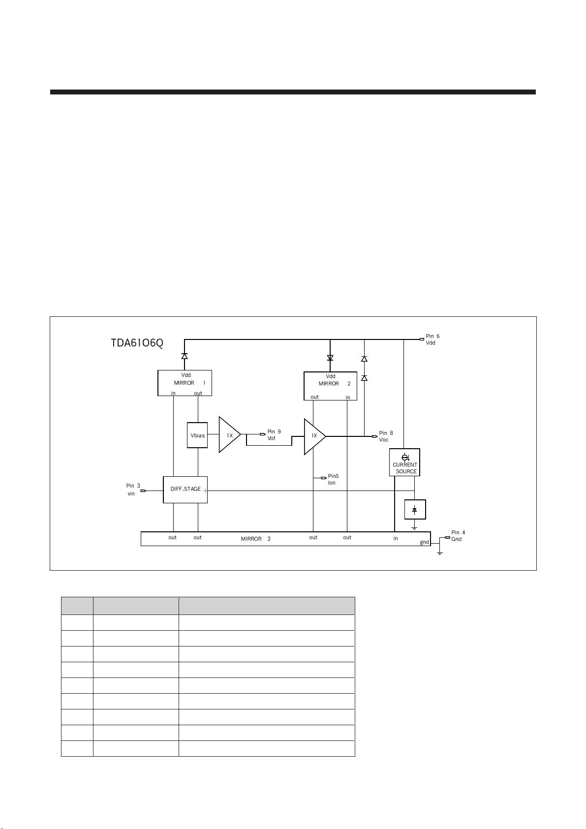
TDA6106Q ( Video Output Amplifier )
(1) General Description
The TDA6106Q is a monolithic video output amplifier (5MHz bandwidth) in a SIL 9 MPpackage, using high-voltage
DMOS technology, and is intended to drive the cathode of CRT directly .
To obtain maximum performance, the amplifier should be used with black-current control.
(2) Feature
•
Black - current measurement output for automatic black current stabilization (ABS)
•
Single supply voltage of 200V
•
Internal protection against positive appearing CRT flash-over discharge
•
Protection against ESD
•
Internal 2.5V reference circuit
•
Controllable switch-off behavior
(3) Block Diagram
–
(4) Pin Description
PIN SYMBOL DESCRIPTION
1 N.C
2 N.C
3 V in inverting input
4 GND ground, substrate
5 I om Black-current measurement output
6 V dd supply voltage high
7 N.C
8 V oc cathode output
9 V of feedback/transient output
23
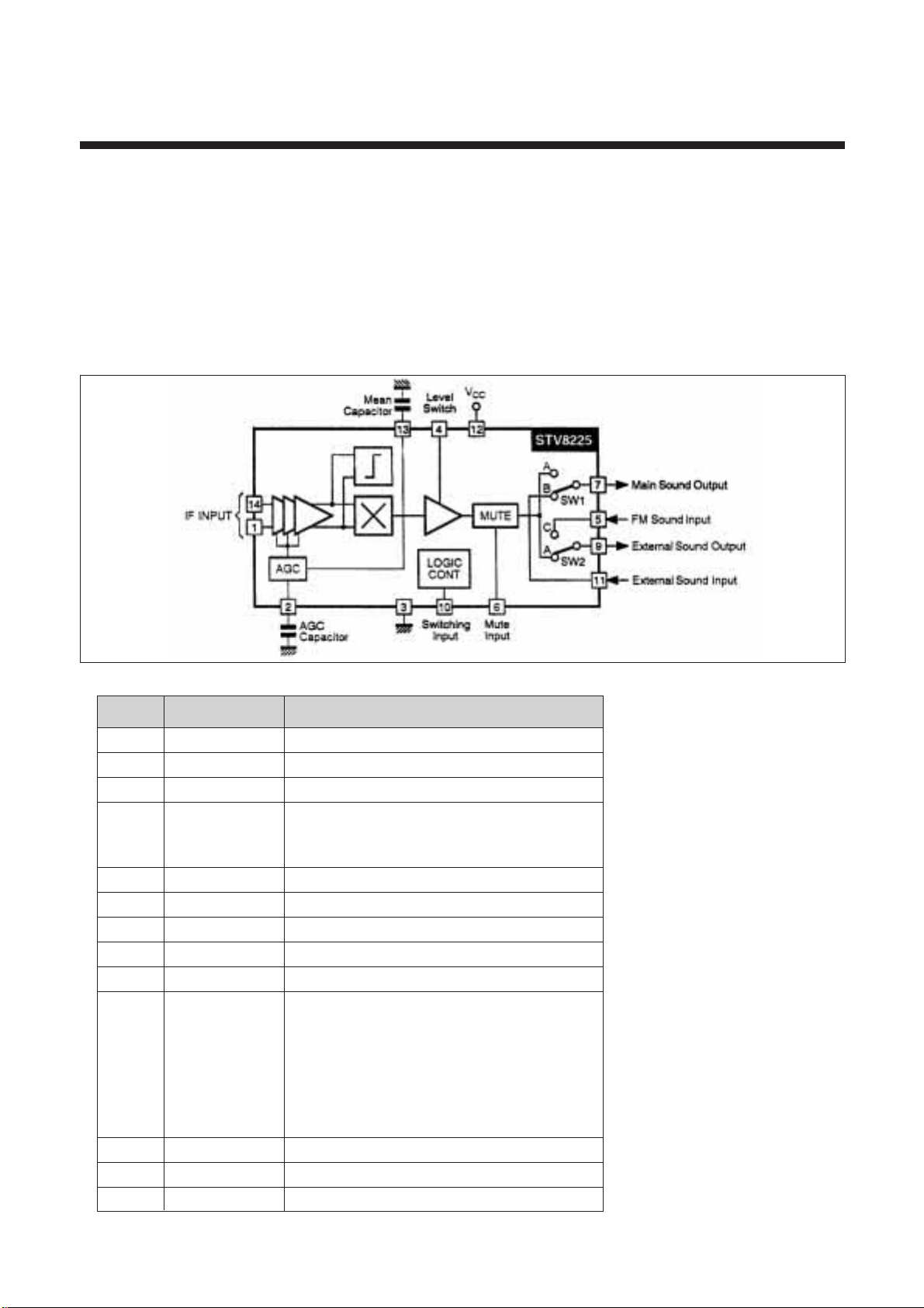
STV8225 ( AM SIF Circuit )
(1) General Description
The STV8225 is intended for the demodulation of the AM sound of the L standard.
(2) Feature
•
sound AM synchronous demodulator
•
AM/FM audio switch and AV/TV audio switch
(3) Block Diagram
(4) Pin Description
PIN SYMBOL DESCRIPTION
1, 14 IF in IF input
2 AGC AGC capacitor
3 GND ground
4 level sw level switch of AF output voltage (pin7,9)
- open : 250 mVrms
- ground : 500 mVrms
5 FM in FM sound input
6 mute mute input
7 main in main sound input
8 n.c
9 ext out external sound output
10 sw in switching input
voltage mode connection
pin7 pin 9
2.3V below TV/FM A C
4.6V below TV/AM A A
6.8V below AV/AM B A
6.8V above AV/FM B C
11 ext in external sound input
12 Vcc supply voltage (+9V)
13 mean cap mean capacitor
24
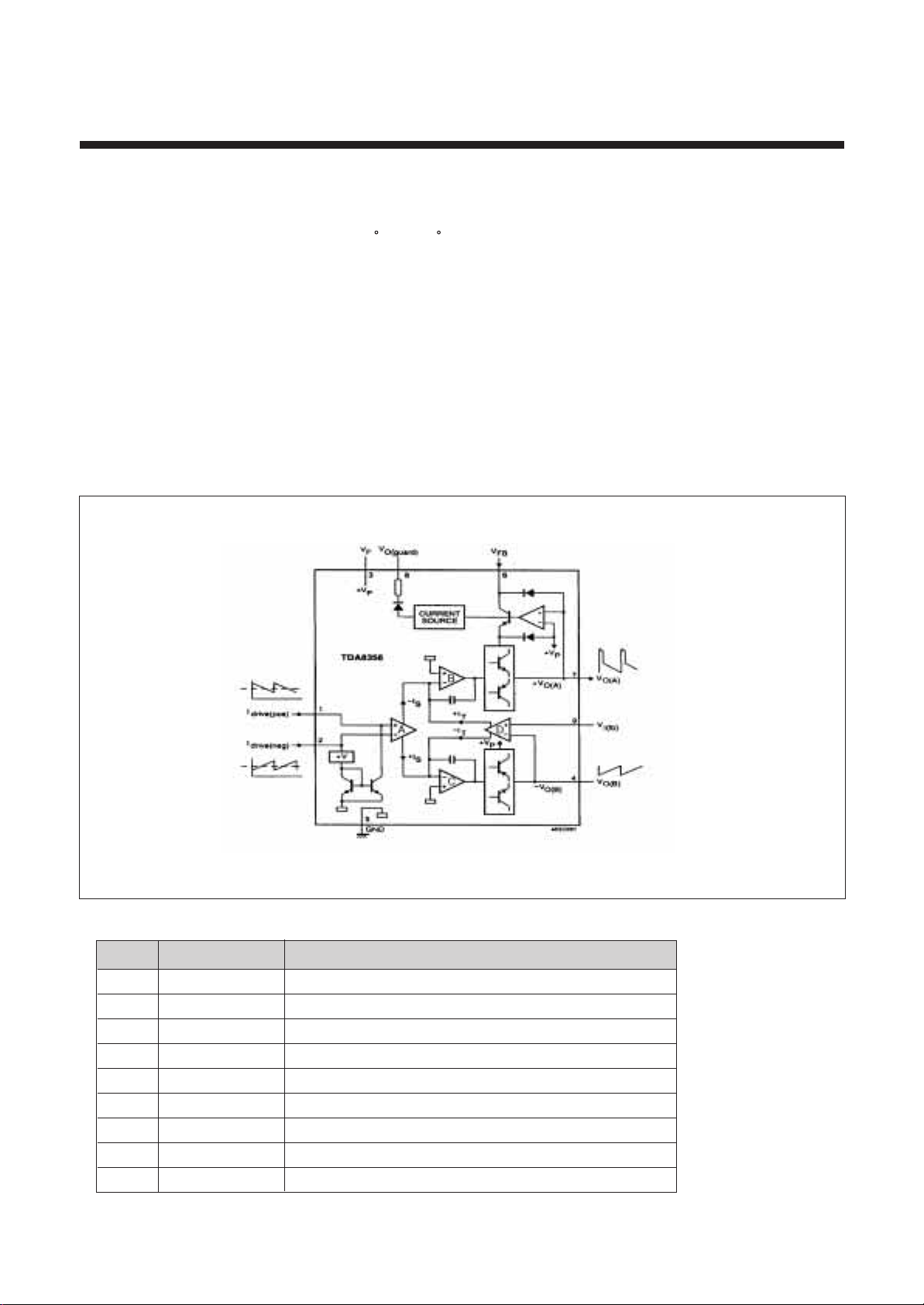
TDA8356 (DC-coupled vertical deflection circuit)
(1) General Description
The TDA8356 is power circuit for use in 90 and 110 color deflection systems for field frequencies of 50 to 120 Hz.
The circuit provides a DC driven vertical deflection output circuit, operating as a high efficient class G system.
(2) Feature
•
High efficient fully DC-coupled vertical output bridge circuit
•
Vertical fly-back switch
•
Guard circuit
•
Protection against : - short circuit of the output pins (7 and 4)
- short circuit of the output pins to Vp
•
Temperature (thermal) protection
•
High EMC immunity because of common mode inputs
(3) Block Diagram
(4) Pin Description
PIN SYMBOL DESCRIPTION
1 I drive (pos) input power stage (positive); include Ii(sb) signal bias
2 I drive (neg) input power stage (negative); include Ii(sb) signal bias
3 V p operating supply voltage
4 V o(b) output voltage B
5 GND ground
6 V fb input fly-back supply voltage
7 V o(a) output voltage A
8 V o(guard) guard output voltage
9 V I(fb) input feedback voltage
25
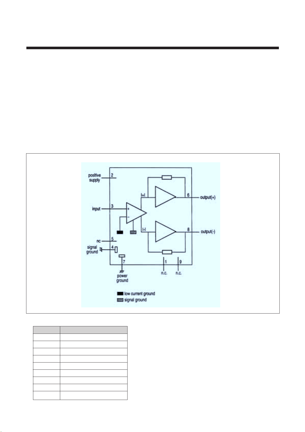
TDA7056 (BTL AUDIO OUTPUT AMPLIFIER)
(1) Features
• No external components
• No switch-on/off clicks
• Good overall stability
• Low power consumption
• Short circuit proof
• ESD protected on all pins
(2) General Description
The TDA7056 is a mono output amplifier contained in a 9 pin medium power package.
The device is designed for batteryfed portable mono recorders, radios and television.
(3)Block Diagram
(4)Pin Description
PIN DESCRIPTION
1 n.c.
2Vp
3 input (+)
4 signal ground
5 n.c.
6 output (+)
7 power ground
8 output (-)
9 n.c.
26
 Loading...