

Page 1
CY7C6431x
CY7C64345, CY7C6435x
enCoRe™ V Full Speed USB Controller
Features
System Bus
6/12/24 MHz Internal Main Oscillator
CPU Core
(M8C)
SROM Flash 32K
SYSTEM RESOURCES
I2C Slave/SPI
Master-Slave
POR and LVD
System Resets
Port 1 Port 0
Sleep and
Watchdog
Full
Speed
USB
Port 3 Port 2
Prog. LDO
SRAM
2048 Bytes
Interrupt
Controller
enCoRe V
CORE
3 16-Bit
Timers
Port 4
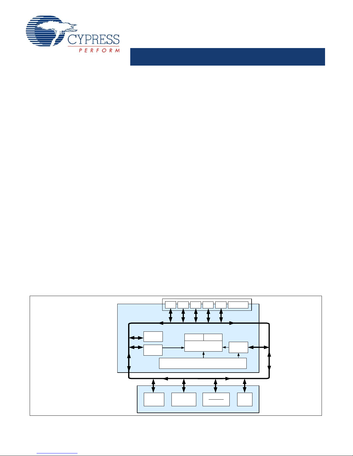
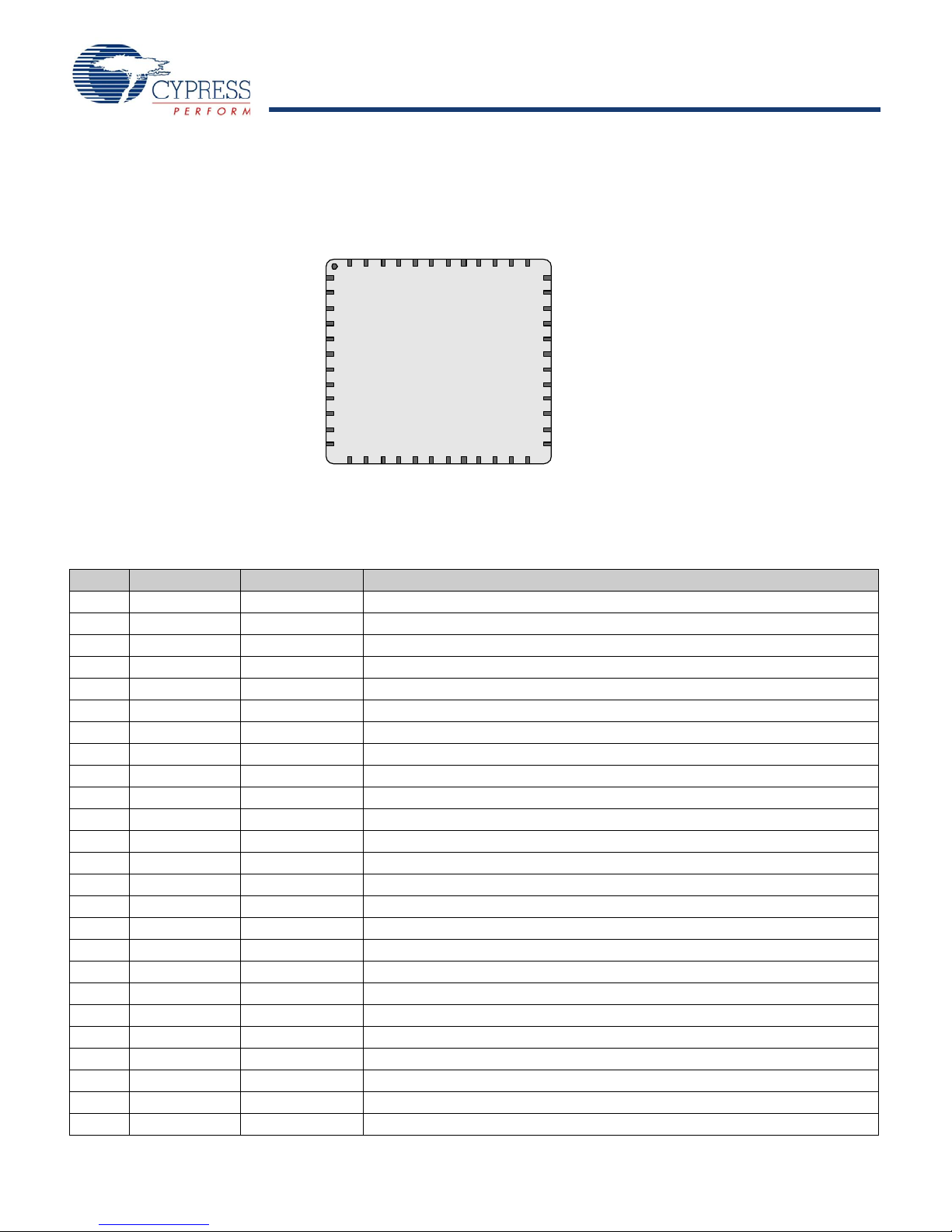
enCoRe V Block Diagram
■ Powerful Harvard Architecture Processor
❐ M8C processor speeds running up to 24 MHz
❐ Low power at high processing speeds
❐ Interrupt controller
❐ 3.0V to 5.5V operating voltage without USB
❐ Operating voltage with USB enabled:
• 3.15 to 3.45V when supply voltage is around 3.3V
• 4.35 to 5.25V when supply voltage is around 5.0V
❐ Temperature range: 0°C to 70°C
■ Flexible On-Chip Memory
❐ Up to 32K Flash program storage
• 50,000 erase and write cycles
• Flexible protection modes
❐ Up to 2048 bytes SRAM data storage
❐ In-System Serial Programming (ISSP)
■ Complete Development Tools
❐ Free development tool (PSoC Designer™)
❐ Full featured, in-circuit emulator and programmer
❐ Full speed emulation
❐ Complex breakpoint structure
❐ 128K trace memory
■ Precision, Programmable Clocking
❐ Crystal-less oscillator with support for an external crystal or
resonator
❐ Internal ±5.0% 6, 12, or 24 MHz main oscillator
• 0.25% accuracy with Oscillator Lock to USB data, no
external components required
• Internal low speed oscillator at 32 kHz for watchdog and
sleep. The frequency range is 19 to 50 kHz with a 32 kHz
typical value
■ Programmable Pin Configurations
❐ 25 mA sink current on all GPIO
❐ Pull Up, High Z, Open Drain, CMOS drive modes on all GPIO
❐ Configurable inputs on all GPIO
❐ Low dropout voltage regulator for Port 1 pins. Programmable
to output 3.0, 2.5, or 1.8V at the I/O pins
❐ Selectable, regulated digital I/O on Port 1
• Configurable input threshol d for Port 1
• 3.0V, 20 mA total Port 1 source current
• Hot-swappable
❐ 5 mA strong drive mode on Ports 0 and 1
■ Full-Speed USB (12 Mbps)
❐ Eight unidirectional endpoints
❐ One bidirectional control endpoint
❐ USB 2.0 compliant
❐ Dedicated 512 bytes buffer
❐ No external crystal required
■ Additional System Resources
❐ Configurable communication speeds
2
❐ I
C slave
• Selectable to 50 kHz, 100 kHz, or 400 kHz
• Implementation requires no clock stretching
• Implementation during sleep modes with less than 100 μA
• Hardware address detection
❐ SPI master and SPI slave
• Configurable between 93.75 kHz and 12 MHz
❐ Three 16-bit timers
❐ 8-bit ADC used to monitor battery voltage or other signals -
with external components
❐ Watchdog and sleep timers
❐ Integrated supervisory circuit
Cypress Semiconductor Corporation • 198 Champion Court • San Jose, CA 95134-1709 • 408-943-2600
Document Number: 001-12394 Rev *G Revised January 30, 2009
[+] Feedback
Page 2

CY7C6431x
CY7C64345, CY7C6435x
Functional Overview
The enCoRe V family of devices are designed to replace multiple
traditional full speed USB microcontroller system components
with one, low cost single-chip programmable component.
Communication peripherals (I2C/SPI), a fast CPU, Flash
program memory, SRAM dat a memory, and configurable I/O are
included in a range of convenient pinouts.
The architecture for this device family, as illustrated in the
“enCoRe V Block Diagram” on page 1, consists of two main
areas: the CPU core and the system resources. Depending on
the enCoRe V package, up to 36 general purpose I/O (GPIO) are
also included.
This product is an enhanced version of Cypress’s successful full
speed USB peripheral controllers. Enhancements include faster
CPU at lower voltage operation, lower current consumption,
twice the RAM and Flash, hot-swappable I/Os, I
address recognition, new very low current sleep mode, and new
package options.
The enCoRe V Core
The enCoRe V Core is a powerful engine that supports a rich
instruction set. It encompasses SRAM for data storage, an
interrupt controller, sleep and watchdog timers, and IMO
(internal main oscillator) and ILO (internal low speed oscillator).
The CPU core, called the M8C, is a powerful processor with
speeds up to 24 MHz. The M8C is a four-MIPS, 8-bit Harvard
architecture microprocessor.
System resources provide additional capability, such as a configurable I
2
C slave and SPI master-slave communication interface
and various system resets supported by the M8C.
Additional System Resources
System resources, some of which have been previously listed,
provide additional capability useful to complete systems.
Additional resources include low voltage detection and power on
reset. The following statements describe the merits of each
system resource.
■ Full speed USB (12 Mbps) with nine configurable endpoints
and 512 bytes of dedicated USB RAM. No external components
are required except two series resistors. It is specified for
commercial temperature USB operation. For reliable USB
operation, ensure the supply voltage is between 4.35V and
5.25V, or around 3.3V.
■ 8 bit on-chip ADC shared between system performance
manager (used to calculate parameters based on temperature
for flash write operations) and the user.
2
■ The I
■ In I
C slave and SPI master-slave module provides 50, 100,
or 400 kHz communication over two wires. SPI communication
over three or four wires runs at speeds of 46.9 kHz to 3 MHz
(lower for a slower system clock).
2
C slave mode, the hardware address recognition feature
reduces the already low power consumption by eliminating the
2
C hardware
need for CPU intervention until a packet addressed to the target
device is received.
■ Low Voltage Detection (LVD) interrupts can signal the appli-
cation of falling voltage levels, while the advanced POR (power
on reset) circuit eliminates the need for a system supervisor.
■ The 5V maximum input, 1.8, 2.5, or 3V selectable output, low
dropout regulator (LDO) provides regulation for I/Os. A register
controlled bypass mode enables the user to disable the LDO.
■ Standard Cypress PSoC IDE tools are available for debugging
the enCoRe V family of parts.
Getting Started
The quickest path to understanding the enCoRe V silicon is by
reading this data sheet and using the PSoC Designer Integrated
Development Environment (IDE). This data sheet is an overview
of the enCoRe V integrated circuit and presents specific pin,
register, and electrical specifications. For in-depth information,
along with detailed programming information, reference the
PSoC Programmable System-on-Chip Technical Reference
Manual, which can be found on http://www.cypress.com/psoc.
For up-to-date Ordering, Packaging, and Electrical Specification
information, reference the latest enCoRe V device data sheets
on the web at http://www.cypress.com.
Development Kits
Development Kits are available online from Cypress at
www.cypress.com/shop and through a growing number of
regional and global distributors, which include Arrow, Avnet,
Digi-Key, Farnell, Future Electronics, and Newark. Under
Product Categories, click USB (Universal Serial Bus) to view a
current list of available items.
Technical Training Modules
Free technical training (on demand, webinars, and workshops)
is available online at www.cypress.com/training. The training
covers a wide variety of topics and skill levels to assist you in
your designs.
Consultants
Certified USB consultants offer everything from technical assistance to completed PSoC designs. T o contact or become a PSoC
Consultant go to www.cypress.com /cypros.
Technical Support
For assistance with technical issues, search KnowledgeBase
articles and forums at www.cypress.com/support. If you cannot
find an answer to your question, call technical support at
1-800-541-4736.
Application Notes
Application notes are an excellent introduction to the wide variety
of possible PSoC designs. They are located here:
www.cypress.com/psoc. Select Application Notes under the
Documentation tab.
Document Number: 001-12394 Rev *G Page 2 of 28
[+] Feedback
Page 3

CY7C6431x
CY7C64345, CY7C6435x
Development Tools
PSoC Designer™ is a Microsoft® Windows-based, integrated
development environment for the enCoRe and PSoC devices.
The PSoC Designer IDE and application runs on Win dows XP
and Windows Vista.
This system provides design database management by project,
an integrated debugger with In-Circuit Emulator, in-system
programming support, and built-in support for third-party assemblers and C compilers.
PSoC Designer also supports C language compilers developed
specifically for the devices in the enCoRe and PSoC families.
PSoC Designer Software Subsystems
Chip-Level View
The chip-level view is a traditional integrated development
environment (IDE) based on PSoC Designer 4.4. You choose a
base device to work with and then select different onboard
analog and digital components called user modules that use the
PSoC blocks. Examples of user modules are ADCs, DACs,
Amplifiers, and Filters. You configure the user modules for your
chosen application and connect them to each other and to the
proper pins. Then you generate your project. This prepopulates
your project with APIs and libraries that you can use to program
your application.
The tool also supports easy development of multiple configurations and dynamic reconfiguration. Dynamic reconfiguration
allows for changing configurations at run time.
System-Level View
The system-level view is a drag-and-drop visual embedded
system design environment based on PSoC Designer.
Hybrid Designs
You can begin in the system-level view, allow it to choose and
configure your user modules, routing, and generate code, then
switch to the chip-level view to gain complete control over
on-chip resources. All views of the project share common code
editor, builder , and common debug, emulation, and programming
tools.
Code Generation Tools
PSoC Designer supports multiple third-party C compilers and
assemblers. The code generation tools work seamlessly within
the PSoC Designer interface and have been tested with a full
range of debugging tools. The choice is yours.
Assemblers. The assemblers allow assembly code to be
merged seamlessly with C code. Link libraries automatically use
absolute addressing or are compiled in relative mode, and linked
with other software modules to get absolute addressing.
C Language Compilers. C language compilers are available
that support the enCoRe and PSoC families of devices. The
products enable you to create complete C programs for the
PSoC family devices.
The optimizing C compilers provide all the features of C tailored
to the PSoC architecture. They come complete with embedded
libraries providing port and bus operations, standard keypad and
display support, and extended math functionality.
Debugger
PSoC Designer has a debug environment that provides
hardware in-circuit emulation, allowing you to test the program in
a physical system while providing an internal view of the PSoC
device. Debugger commands allow the designer to read and
program flash, read and write data memory, read and write I/O
registers, read and write CPU registers, set and clear breakpoints, and provide program run, halt, and step control. The
debugger also allows the designer to create a trace buffer of
registers and memory locations of interest.
Online Help System
The online help system displays online, context-sensitive help
for the user. Designed for procedural help and quick reference,
each functional subsystem has its own context-sensitive help.
This system also provides tutorials and links to FAQs and an
Online Support Forum to aid the designer in getting started.
In-Circuit Emulator
A low cost, high functionality ICE (In-Circuit Emulator) is
available for development support. This hardware has the
capability to program single devices.
The emulator consists of a base unit that connects to the PC by
way of a USB port. The base unit is universal and operates with
all enCoRe and PSoC devices. Emulation pods for each device
family are available separately. The emulation pod takes the
place of the PSoC device in the target board and performs full
speed (24 MHz) operation.
Document Number: 001-12394 Rev *G Page 3 of 28
[+] Feedback
Page 4

CY7C6431x
CY7C64345, CY7C6435x
Designing with PSoC Designer
The development process for the enCoRe V device differs from
that of a traditional fixed function microprocessor. Powerful
PSoC Designer tools get the core of your design up and running
in minutes instead of hours.
The development process can be summarized in the following
four steps:
1. Select Components
2. Configure Components
3. Organize and Connect
4. Generate, Verify, and Debug
Select Components
The chip-level view provides a library of pre-built, pre-tested
hardware peripheral components. These components are called
“user modules.” User modules make selecting and implementing
peripheral devices simple, and come in analog, digital, and
mixed-signal varieties.
Configure Components
Each of the components you select establishes the basic register
settings that implement the selected function. They also provide
parameters and properties that allow you to tailor their precise
configuration to your particular application.
The chip-level user modules are documented in data sheets that
are viewed directly in PSoC Designer. These data sheets explain
the internal operation of the component and provide performance specifications. Each data sheet describes the use of each
user module parameter and contains other information you may
need to successfully implement your design.
Generate, Verify, and Debug
When you are ready to test the hardware configuration or move
on to developing code for the project, you perform the “Generate
Configuration Files” step. This causes PSoC Designer to
generate source code that automatically configures the device to
your specification and provides the software for the system.
Both system-level and chip-level designs generate software
based on your design. The chip-level design provides application
programming interfaces (APIs) with high level functions to
control and respond to hardware events at run time and interrupt
service routines that you can adapt as needed. The system-level
design also generates a C main() program that completely
controls the chosen application and contains placeholders for
custom code at strategic positions allowing you to further refine
the software without disrupting the generated code.
A complete code development environment allows you to
develop and customize your applications in C, assembly
language, or both.
The last step in the development process takes place inside
PSoC Designer’s Debugger (access by clicking the Connect
icon). PSoC Designer downloads the HEX image to the In-Circuit
Emulator (ICE) where it runs at full speed. PSoC Designer
debugging capabilities rival those of systems costing many times
more. In addition to traditional single-step, run-to-breakpoint and
watch-variable features, the debug interface provides a large
trace buffer and allows you to define complex breakpoint events
that include monitoring address and data bus values, memory
locations and external signals.
Organize and Connect
You build signal chains at the chip level by interconnecting user
modules to each other and the I/O pins, or connect system-level
inputs, outputs, and communication interfaces to each other with
valuator functions. In the chip-level view, you perform the
selection, configuration, and routing so that you have complete
control over the use of all on-chip resources.
Document Number: 001-12394 Rev *G Page 4 of 28
[+] Feedback
Page 5
CY7C6431x
CY7C64345, CY7C6435x
Document Conventions
Acronyms Used
The following table lists the acronyms that are used in this
document.
Acronym Description
API application programming interface
CPU central processing unit
GPIO general purpose IO
ICE in-circuit emulator
ILO internal low speed oscillator
IMO internal main oscillator
IO input/output
LSb least significant bit
LVD low voltage detect
MSb most significant bit
POR pow er on rese t
PPOR precision power on reset
PSoC® Programmable System-on-Chip™
SLIMO slow IMO
SRAM static random access memory
Units of Measure
A units of measure table is located in the Electrical Specifications
section. Table7 on page 13 lists all the abbreviations used to
measure the enCoRe V devices.
Numeric Naming
Hexadecimal numbers are represented with all letters in
uppercase with an appended lowercase ‘h’ (for example, ‘14h’ or
‘3Ah’). Hexadecimal numbers may also be represented by a ‘0x’
prefix, the C coding convention. Binary numbers have an
appended lowercase ‘b’ (for example, 01010100b’ or
‘01000011b’). Numbers not indicated by an ‘h’, ‘b’, or 0x are
decimal.
Document Number: 001-12394 Rev *G Page 5 of 28
[+] Feedback
Page 6
CY7C6431x
CY7C64345, CY7C6435x
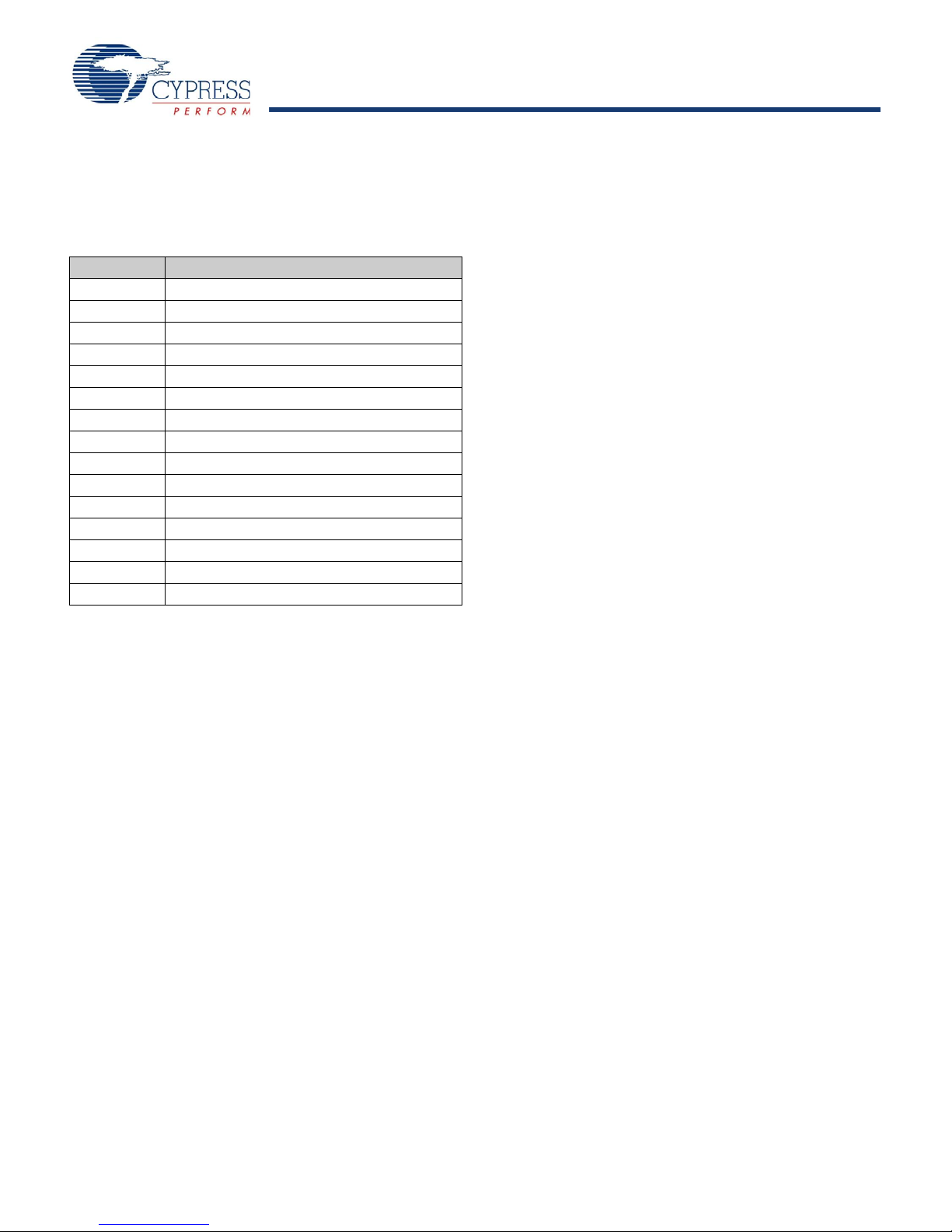
Pin Configuration
D+
QFN
(Top View)
P2[3]
P1[5]
P1[1]
Vss
16
15
14
13
P0[1]
P0[3]
P0[7]
P0[4]
5
6
7
8
Vdd
P1[0]
P1[7]
P1[4]
XRES
P2[5]
D–
1
2
3
4
12
11
10
9
Notes
1. During power up or reset event, device P1[0] and P1[1] may disturb the I2C bus. Use alternate pins if issues are encountered.
2. These are the in-system serial programming (ISSP) pins that are not High Z at power on reset (POR).
The enCoRe V USB device is available in a variety of packages which are listed and illustrated in the subsequent tables.
16-Pin Part Pinout
Figure 1. CY7C64315/CY7C64316 16-Pin enCoRe V Device
Ta bl e 1. 16-Pin Part Pinout (QFN)
Pin No. Type Name Description
1 I/O P2[3] Digital I/O, Crystal Input (Xin)
2 IOHR P1[7] Digital I/O, SPI SS, I2C SCL
3 IOHR P1[5] Digital I/O, SPI MISO, I2C SDA
4 IOHR P1[1]
5 Power Vss Ground connection
6 USB line D+ USB PHY
7 USB line D– USB PHY
8 Power Vdd Supply
9 IOHR P1[0]
10 IOHR P1[4] Digital I/O, optional external clock input (EXTCLK)
11 Input XRES Active high external reset with internal pull down
12 IOH P0[4] Digital I/O
13 IOH P0[7] Digital I/O
14 IOH P0[3] Digital I/O
15 IOH P0[1] Digital I/O
16 I/O P2[5] Digital I/O, Crystal Output (Xout)
(1, 2)
(1, 2)
Digital I/O, ISSP CLK, 12C SCL, SPI MOSI
Digital I/O, ISSP DAT A, I2C SDA, SPI CLK
LEGEND I = Input, O = Output, OH = 5 mA High Output Drive, R = Regulated Output
Document Number: 001-12394 Rev *G Page 6 of 28
[+] Feedback
Page 7
CY7C6431x
CY7C64345, CY7C6435x
P0[1]
P2[5]
P2[3]
P2[1]
P1[7]
QFN
(Top View)
9
10111213141516
1
2
3
4
5
6
7
8
24
23
22
21
20
19
18
17
32313029282726
25
Vss
P0[3]
P0[7]
Vdd
P0[6]
P0[4]
P0[2]
P1[5]
P1[1]
P0[0]
P2[6]
P3[0]
XRES
Vss
D+
D–
Vdd
P1[0]
P1[2]
P1[4]
P1[6]
P2[4]
P2[2]
P2[0]
P3[2]
P0[5]
P1[3]
32-Pin Part Pinout
Figure 2. CY7C64343/CY7C64345 32-Pin enCoRe V USB Device
Ta bl e 2. 32-Pin Part Pinout (QFN)
Pin No. Type Name Description
1 IOH P0[1] Digital I/O
2 I/O P2[5] Digital I/O, Crystal Output (Xout)
3 I/O P2[3] Digital I/O, Crystal Input (Xin)
4 I/O P2[1] Digital I/O
5 IOHR P1[7] Digital I/O, I2C SCL, SPI SS
6 IOHR P1[5] Digital I/O, I2C SDA, SPI MISO
7 IOHR P1[3] Digital I/O, SPI CLK
8 IOHR P1[1]
9 Power Vss Ground
10 I/O D+ USB PHY
11 I/O D– USB PHY
12 Power Vdd Supply voltage
13 IOHR P1[0]
14 IOHR P1[2] Digital I/O
15 IOHR P1[4] Digital I/O, optional external clock input (EXTCLK)
16 IOHR P1[6] Digital I/O
17 Reset XRES Active high external reset with internal pull down
18 I/O P3[0] Digital I/O
19 I/O P3[2] Digital I/O
20 I/O P2[0] Digital I/O
21 I/O P2[2] Digital I/O
22 I/O P2[4] Digital I/O
23 I/O P2[6] Digital I/O
24 IOH P0[0] Digital I/O
25 IOH P0[2] Digital I/O
26 IOH P0[4] Digital I/O
27 IOH P0[6] Digital I/O
28 Power Vdd Supply voltage
29 IOH P0[7] Digital I/O
30 IOH P0[5] Digital I/O
31 IOH P0[3] Digital I/O
32 Power Vss Ground
CP Power Vss En sure the center pad is connected to ground
LEGEND I = Input, O = Output, OH = 5 mA High Output Drive, R = Regulated Output
Document Number: 001-12394 Rev *G Page 7 of 28
(1, 2)
Digital I/O, ISSP CLK, I2C SCL, SPI MOSI
(1, 2)
Digital I/O, ISSP DAT A, I2C SDA, SPI CLK
[+] Feedback
Page 8
CY7C6431x
CY7C64345, CY7C6435x
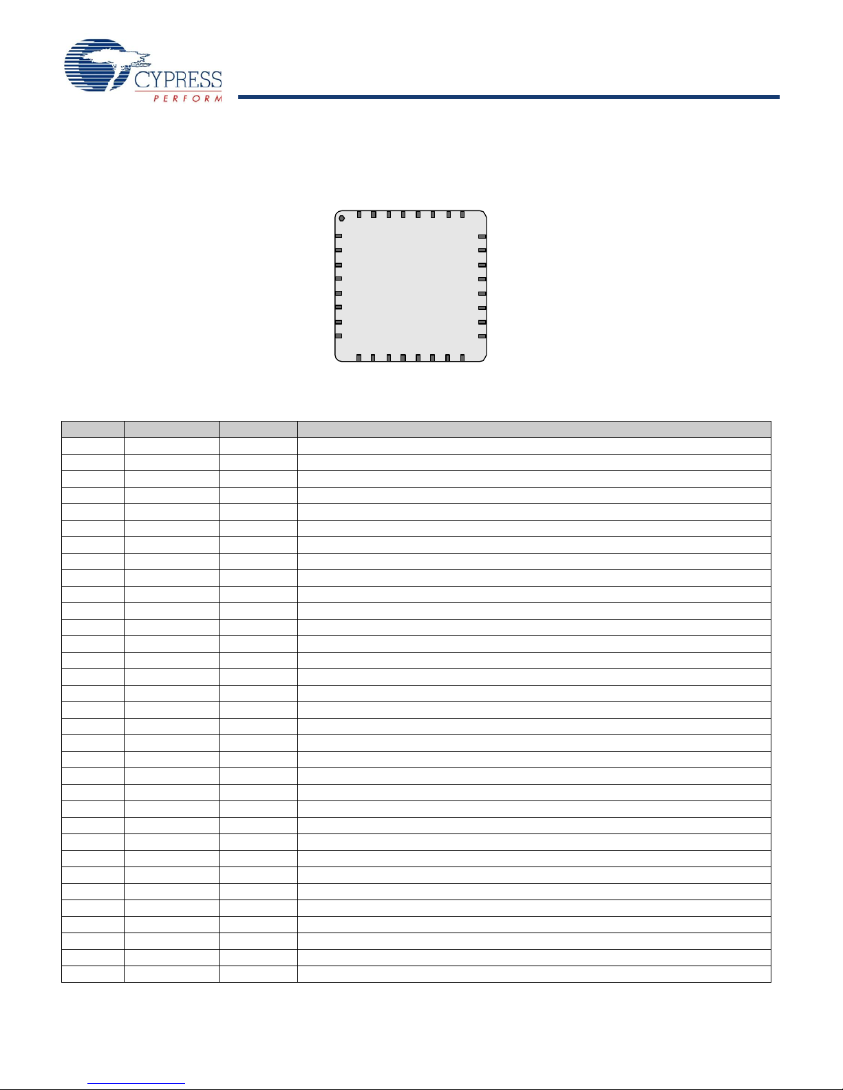
48-Pin Part Pinout
QFN
(Top View)
P0[1]
Vss
P0[3]
P0[5]
P0[7]
Vdd
P0[6]
10
11
12
P2[7]
P2[5]
P2[3]
P2[1]
P4[3]
P4[1]
P3[7]
P3[5]
P3[3]
35
34
33
32
31
30
29
28
27
26
25
36
4847464544
43424140393837
P0[2]
P0[0]
P2[6]
P2[4]
P2[2]
P2[0]
P3[2]
P3[0]
XRES
P1[6]
P0[4]
1
2
3
4
5
6
7
8
9
131415161718192021
22
23
24
NC
NC
P1[3]
P1[1]
Vss
D+
D-
Vdd
P1[0]
P1[2]
P1[4]
NC
P3[1]
P1[7]
P1[5]
P3[4]
P3[6]
P4[0]
P4[2]
NC
NC
Figure 3. CY7C64355/CY7C64356 48-Pin enCoRe V USB Device
Ta bl e 3. 48-Pin Part Pinout (QFN)
Pin No. Type Pin Name Description
1NCNC No connection
2 I/O P2[7] Digital I/O
3 I/O P2[5] Digital I/O, Crystal Out (Xout)
4 I/O P2[3] Digital I/O, Crystal In (Xin)
5 I/O P2[1] Digital I/O
6 I/O P4[3] Digital I/O
7 I/O P4[1] Digital I/O
8 I/O P3[7] Digital I/O
9 I/O P3[5] Digital I/O
10 I/O P3[3] Digital I/O
11 I/O P3[1] Digital I/O
12 IOHR P1[7] Digital I/O, I2C SCL, SPI SS
13 IOHR P1[5] Digital I/O, I2C SDA, SPI MISO
14 NC NC No connection
15 NC NC No connection
16 IOHR P1[3] Digital I/O, SPI CLK
17 IOHR P1[1]
18 Power Vss Supply ground
19 I/O D+ USB
20 I/O D– USB
21 Power Vdd Supply voltage
22 IOHR P1[0]
23 IOHR P1[2] Digital I/O,
24 IOHR P1[4] Digital I/O, optional external clock input (EXTCLK)
25 IOHR P1[6] Digital I/O
Document Number: 001-12394 Rev *G Page 8 of 28
(1, 2)
(1, 2)
Digital I/O, ISSP CLK, I2C SCL, SPI MOSI
Digital I/O, ISSP DATA, I2C SDA, SPI CLK
[+] Feedback
Page 9
CY7C6431x
CY7C64345, CY7C6435x
Ta bl e 3. 48-Pin Part Pinout (QFN) (continued)
Pin No. Type Pin Name Description
26 XRES Ext Reset Active high external reset with internal pull down
27 I/O P3[0] Digital I/O
28 I/O P3[2] Digital I/O
29 I/O P3[4] Digital I/O
30 I/O P3[6] Digital I/O
31 I/O P4[0] Digital I/O
32 I/O P4[2] Digital I/O
33 I/O P2[0] Digital I/O
34 I/O P2[2] Digital I/O
35 I/O P2[4] Digital I/O
36 I/O P2[6] Digital I/O
37 IOH P0[0] Digital I/O
38 IOH P0[2] Digital I/O
39 IOH P0[4] Digital I/O
40 IOH P0[6] Digital I/O
41 Power Vdd Supply voltage
42 NC NC No connection
43 NC NC No connection
44 IOH P0[7] Digital I/O
45 IOH P0[5] Digital I/O
46 IOH P0[3] Digital I/O
47 Power Vss Supply ground
48 IOH P0[1] Digital I/O
LEGEND I = Input, O = Output, OH = 5 mA High Output Drive, R = Regulated Output
Document Number: 001-12394 Rev *G Page 9 of 28
[+] Feedback
Page 10

CY7C6431x
CY7C64345, CY7C6435x
Register Reference
The section discusses the registers of the enCoRe V device. It lists all the registers in mapping tables, in address order.
Register Conventions
The register conventions specific to this section are listed in the
following table.
Table 4. Register Conventions
Convention Description
R Read register or bits
W Write register or bits
L Logical register or bits
C Clearable register or bits
# Access is bit specific
Register Mapping Tables
The enCoRe V device has a total register address space of 512
bytes. The register space is also referred to as IO space and is
broken into two parts: Bank 0 (user space) and Bank 1 (configuration space). The XIO bit in the Flag register (CPU_F) determines which bank the user is currently in. When the XIO bit is
set, the user is said to be in the “extended” address space or the
“configuration” registers.
Document Number: 001-12394 Rev *G Page 10 of 28
[+] Feedback
Page 11

CY7C6431x
CY7C64345, CY7C6435x
Table 5. Register Map Bank 0 Table: User Space
Name Addr (0,Hex) Access Name Addr (0,Hex) Access Name Addr (0,Hex) Access Name Addr (0,Hex) Access
PRT0DR 00 RW EP1_CNT0 40 # 80 C0
PRT0IE 01 RW EP1_CNT1 41 RW 81 C1
PRT1DR 04 RW EP3_CNT0 44 # 84 C4
PRT1IE 05 RW EP3_CNT1 45 RW 85 C5
PRT2DR 08 RW EP5_CNT0 48 # 88 I2C_XCFG C8 RW
PRT2IE 09 RW EP5_CNT1 49 RW 89 I2C_XSTAT C9 R
PRT3DR 0C RW EP7_CNT0 4C # 8C I2C_CP CC R
PRT3IE 0D RW EP7_CNT1 4D RW 8D CPU_BP CD RW
PRT4DR 10 RW 50 90 CUR_PP D0 RW
PRT4IE 11 RW 51 91 STK_PP D1 RW
SPI_TXR 29 W PMA13_DR 69 RW A9 E9
SPI_RXR 2A R PMA14_DR 6A RW AA EA
SPI_CR 2B # PMA15_DR 6B RW AB EB
USB_SOF0 31 R 71 PT0_DAT A1 B1 RW F1
USB_SOF1 32 R 72 PT0_DAT A0 B2 RW F2
USB_CR0 33 RW 73 PT1_CFG B3 RW F3
USBIO_CR0 34 # 74 PT1_DATA1 B4 RW F4
USBIO_CR1 35 # 75 PT1_DATA0 B5 RW F5
EP0_CR 36 # 76 PT2_CFG B6 RW F6
EP0_CNT0 37 # 77 PT2_DATA1 B7 RW CPU_F F7 RL
EP0_DR0 38 RW 78 PT2_DATA0 B8 RW F8
EP0_DR1 39 RW 79 B9 F9
EP0_DR2 3A RW 7A BA FA
EP0_DR3 3B RW 7B BB FB
EP0_DR4 3C RW 7C BC FC
EP0_DR5 3D RW 7D BD FD
EP0_DR6 3E RW 7E BE CPU_SCR1 FE #
EP0_DR7 3F RW 7F BF CPU_SCR0 FF #
Gray fields are reserved; do not access these fields. # Access is bit specific.
02 EP2_CNT0 42 # 82 C2
03 EP2_CNT1 43 RW 83 C3
06 EP4_CNT0 46 # 86 C6
07 EP4_CNT1 47 RW 87 C7
0A EP6_CNT0 4A # 8A I2C_ADDR CA RW
0B EP6_CNT1 4B RW 8B I2C_BP CB R
0E EP8_CNT0 4E # 8E CPU_CP CE R
0F EP8_CNT1 4F RW 8F I2C_BUF CF RW
12 52 92 D2
13 53 93 IDX_PP D3 RW
14 54 94 MVR_PP D4 RW
15 55 95 MVW_PP D5 RW
16 56 96 I2C_CFG D6 RW
17 57 97 I2C_SCR D7 #
18 PMA0_DR 58 RW 98 I2C_DR D8 RW
19 PMA1_DR 59 RW 99 D9
1A PMA2_DR 5A RW 9A INT_CLR0 DA RW
1B PMA3_DR 5B RW 9B INT_CLR1 DB RW
1C PMA4_DR 5C RW 9C INT_CLR2 DC RW
1D PMA5_DR 5D RW 9D INT_CLR3 DD RW
1E PMA6_DR 5E RW 9E INT_MSK2 DE RW
1F PMA7_DR 5F RW 9F INT_MSK1 DF RW
20 60 A0 INT_MSK0 E0 RW
21 61 A1 INT_SW_EN E1 RW
22 62 A2 INT_VC E2 RC
23 63 A3 RES_WDT E3 W
24 PMA8_DR 64 RW A4 INT_MSK3 E4 RW
25 PMA9_DR 65 RW A5 E5
26 PMA10_DR 66 RW A6 E6
27 PMA11_DR 67 RW A7 E7
28 PMA12_DR 68 RW A8 E8
2C TMP_DR0 6C RW AC EC
2D TMP_DR1 6D RW AD ED
2E TMP_DR2 6E RW AE EE
2F TMP_DR3 6F RW AF EF
30 70 PT0_CFG B0 RW F0
Document Number: 001-12394 Rev *G Page 11 of 28
[+] Feedback
Page 12

CY7C6431x
CY7C64345, CY7C6435x
Table 6. Register Map Bank 1 Table: Configuration Space
Name Addr (1,Hex) Access Name Addr (1,Hex) Access Name Addr (1,Hex) Access Name Addr (1,Hex) Access
PRT0DM0 00 RW PMA4_RA 40 RW 80 C0
PRT0DM1 01 RW PMA5_RA 41 RW 81 C1
PRT1DM0 04 RW PMA8_WA 44 RW 84 C4
PRT1DM1 05 RW PMA9_WA 45 RW 85 C5
PRT2DM0 08 RW PMA12_WA 48 RW 88 C8
PRT2DM1 09 RW PMA13_WA 49 RW 89 C9
PRT3DM0 0C RW PMA8_RA 4C RW 8C CC
PRT3DM1 0D RW PMA9_RA 4D RW 8D CD
PRT4DM0 10 RW PMA12_RA 50 RW 90 D0
PRT4DM1 11 RW PMA13_RA 51 RW 91 D1
SPI_CFG 29 RW 69 A9 ILO_TR E9 W
USB_CR1 30 # 70 B0 F0
USBIO_CR2 33 RW 73 B3 F3
PMA0_WA 34 RW 74 B4 F4
PMA1_WA 35 RW 75 B5 F5
PMA2_WA 36 RW 76 B6 F6
PMA3_WA 37 RW 77 B7 CPU_F F7 RL
PMA4_WA 38 RW 78 B8 F8
PMA5_WA 39 RW 79 B9 F9
PMA6_WA 3A RW 7A BA FA
PMA7_WA 3B RW 7B BB FB
PMA0_RA 3C RW 7C BC FC
PMA1_RA 3D RW 7D BD FD
PMA2_RA 3E RW 7E BE FE
PMA3_RA 3F RW 7F BF FF
Gray fields are reserved; do not access these fields. # Access is bit specific.
02 PMA6_RA 42 RW 82 C2
03 PMA7_RA 43 RW 83 C3
06 PMA10_WA 46 RW 86 C6
07 PMA11_WA 47 RW 87 C7
0A PMA14_WA 4A RW 8A CA
0B PMA15_WA 4B RW 8B CB
0E PMA10_RA 4E RW 8E CE
0F PMA11_RA 4F RW 8F CF
12 PMA14_RA 52 RW 92 D2
13 PMA15_RA 53 RW 93 D3
14 EP1_CR0 54 # 94 D4
15 EP2_CR0 55 # 95 D5
16 EP3_CR0 56 # 96 D6
17 EP4_CR0 57 # 97 D7
18 EP5_CR0 58 # 98 D8
19 EP6_CRO 59 # 99 D9
1A EP7_CR0 5A # 9A DA
1B EP8_CR0 5B # 9B DB
1C 5C 9C IO_CFG DC RW
1D 5D 9D OUT_P1 DD RW
1E 5E 9E DE
1F 5F 9F DF
20 60 A0 OSC_CR0 E0 RW
21 61 A1 ECO_CFG E1 #
22 62 A2 OSC_CR2 E2 RW
23 63 A3 VLT_CR E3 RW
24 64 A4 VLT_CMP E4 R
25 65 A5 E5
26 66 A6 E6
27 67 A7 E7
28 68 A8 IMO_TR E8 W
2A 6A AA EA
2B 6B AB SLP_CFG EB RW
2C TMP_DR0 6C RW AC SLP_CFG2 EC RW
2D TMP_DR1 6D RW AD SLP_CFG3 ED RW
2E TMP_DR2 6E RW AE EE
2F TMP_DR3 6F RW AF EF
31 71 B1 F1
32 72 B2 F2
Document Number: 001-12394 Rev *G Page 12 of 28
[+] Feedback
Page 13

CY7C6431x
CY7C64345, CY7C6435x
Electrical Specifications
5.5V
750 kHz
24 MHz
CPU Frequency
Vdd Voltage
3.0V
3 MHz
V
a
l
i
d
O
p
e
r
a
t
i
n
g
R
e
g
i
o
n
5.5V
750 kHz 6 MHz 24 MHz
IMO Frequency
Vdd Voltage
3 MHz
3.0V
SLIMO
Mode
= 01
12 MHz
SLIMO
Mode
= 00
SLIMO
Mode
= 10
This section presents the DC and AC electrical specifications of the e nCoRe V USB devices. For the most up to date electrical
specifications, verify that you have the most recent data sheet available by visiting the company web site at http://www.cypress.com
Figure 4. Voltage versus CPU Frequency Figure 5. IMO Frequency Trim Options
The following table lists the units of measure that are used in this section.
Table 7. Units of Measure
Symbol Unit of Measure Symbol Unit of Measure
o
C degree Celsius μW microwatts
dB decibels mA milli-ampere
fF femto farad ms milli-second
Hz hertz mV milli-volts
KB 1024 bytes nA nanoampere
Kbit 1024 bits ns nanosecond
kHz kilohertz nV nanovolts
kΩ kilohm Ω ohm
MHz megahertz pA picoampere
MΩ megaohm pF picofarad
μA microampere pp peak-to-peak
μF microfarad ppm parts per million
μH microhenry ps picosecond
μs microsecond sps samples per second
μV microvolts s sigma: one standard de viation
μVrms microvolts root-mean-square V volts
Document Number: 001-12394 Rev *G Page 13 of 28
[+] Feedback
Page 14

CY7C6431x
CY7C64345, CY7C6435x
ADC Electrical Specifications
Table 8. ADC Electrical Specifications
Symbol Description Min Typ Max Units Conditions
Input
Input Voltage Range Vss 1.3 V This gives 72% of maximum code
Input Capacitance 5 pF
Resolution 8 Bits
8-Bit Sample Rate 23.4375 ksps Data Clock set to 6 MHz. Sample
Rate = 0.001/(2^Resolution/Data
clock)
DC Accuracy
DNL -1 +2 LSb For any configuration
INL -2 +2 LSb For any configuration
Offset Error 0 15 90 mV
Operating Current 275 350 μA
Data Clock 2.25 12 MHz Source is chip’s internal main oscil-
Monotonicity Not guaranteed. See DNL
Power Supply Rejection Ratio
PSRR (Vdd>3.0V) 24 dB
PSRR (2.2 < Vdd < 3.0) 30 dB
PSRR (2.0 < Vdd < 2.2) 12 dB
PSRR (Vdd < 2.0) 0 dB
Gain Error 1 5 %FSR For any resolution
Input Resistance 1/(500fF*D
ata-Clock)
1/(400fF*D
ata-Clock)
1/(300fF*D
ata-Clock)
lator. See AC chip level specifications for accuracy.
Ω Equivalent switched cap input
resistance for 8-, 9-, or 10-bit
resolution.
Document Number: 001-12394 Rev *G Page 14 of 28
[+] Feedback
Page 15

CY7C6431x
CY7C64345, CY7C6435x
Electrical Characteristics
Notes
3. Higher storage temperatures reduce data retention time. Recommended storage temperatu re is +25°C ± 25°C. Extended durati on storage te mperatures above 85
o
C
degrade reliability.
4. Human Body Model ESD.
5. According to JESD78 standard.
6. The temperature rise from ambient to junction is p ackage specific. Se e Package Handling on page 25. The user must limit the power consumptio n to comply with this
requirement.
Absolute Maximum Ratings
Storage Temperature (T
Supply Voltage Relative to Vss (Vdd)............. -0.5V to +6.0V
DC Input Voltage (V
IO
DC Voltage Applied to Tri-state (V
Maximum Current into any Port Pin (I
Electrostatic Discharge Voltage (ESD)
Latch-up Current (LU)
(3)
)
-55oC to 125oC (Typical +25oC)
STG
)....................Vss - 0.5V to Vdd + 0.5V
)Vss - 0.5V to Vdd + 0.5V
IOZ
). -25mA to +50 mA
MIO
(4)
....................2000V
(5)
................................. ... ...... 200 mA
Operating Conditions
Ambient Te mperature (TA)..................................0oC to 70oC
Operational Die Temperature (T
(6)
)
...................0oC to 85oC
J
DC Electrical Characteristics
DC Chip Level Specifications
Table 9 lists guaranteed maximum and minimum specifications for the entire voltage and temperature ranges.
Table 9. DC Chip Level Specifications
Parameter Description Conditions Min Typ Max Units
Vdd Supply Volt age See table titled DC POR and LVD
Specifications on page 17.
I
DD24,3
Supply Current, IMO = 24 MHz Conditions are Vdd = 3.0V, TA = 25oC,
CPU = 24 MHz,
No USB/I2C/SPI.
I
DD12,3
Supply Current, IMO = 12 MHz Conditions are Vdd = 3.0V, TA = 25oC,
CPU = 12 MHz,
No USB/I2C/SPI.
I
DD6,3
Supply Current, IMO = 6 MHz Conditions are Vdd = 3.0V, TA = 25oC,
CPU = 6 MHz,
No USB/I2C/SPI.
I
SB1,3
I
SB0,3
I
DD24,5
Standby Current with POR, LVD, and
Sleep Timer
Vdd = 3.0V, TA = 25oC, I/O regulator
turned off.
Deep Sleep Current Vdd = 3.0V, TA = 25oC, I/O regulator
turned off.
Supply Current, IMO = 24 MHz Conditions are Vdd = 5.0V, TA = 25oC,
CPU = 24 MHz,
No USB/I2C/SPI.
I
DD12,5
Supply Current, IMO = 12 MHz Conditions are Vdd = 5.0V, TA = 25oC,
CPU = 12 MHz,
No USB/I2C/SPI.
I
DD6,5
Supply Current, IMO = 6 MHz Conditions are Vdd = 5.0V, TA = 25oC,
CPU = 6 MHz,
No USB/I2C/SPI.
I
SB1,5
I
SB0,5
Standby Current with POR, LVD, and
Sleep Timer
Vdd = 5.0V, TA = 25oC, I/O regulator
turned off.
Deep Sleep Current Vdd = 5.0V, TA = 25oC, I/O regulator
turned off.
3.0 – 5.5 V
– – 3.1 mA
– – 2.0 mA
– – 1.5 mA
– – 1.5 μA
– 0.1 – μA
– mA
– mA
– mA
– μA
– – μA
Document Number: 001-12394 Rev *G Page 15 of 28
[+] Feedback
Page 16

CY7C6431x
CY7C64345, CY7C6435x
Table 10.DC Characteristics – USB Interface
Symbol Description Conditions Min Typ Max Units
Rusbi USB D+ Pull Up Resistance With idle bus 0.900 - 1.575 kΩ
Rusba USB D+ Pull Up Resistance While receiving traffic 1.425 - 3.090 kΩ
Vohusb Static Output High 2.8 - 3.6 V
Volusb Static Output Low -0.3V
Vdi Differential Input Sensitivity 0.2 - V
Vcm Differential Input Common Mode Range 0.8 - 2.5 V
Vse Single Ended Receiver Threshold 0.8 - 2.0 V
Cin Transceiver Capacitance - 50 pF
Iio High Z State Data Line Leakage On D+ or D- line -10 - +10 μA
Rps2 PS/2 Pull Up Resistance 3 5 7 kΩ
Rext External USB Series Resistor In series with each USB pin 21.76 24.0 24.24 Ω
DC General Purpose IO Specifications
Table 11 lists guaranteed maximum and minimum specifications for the voltage and temperature ranges: 3.0V to 5.5V and 0°C ≤ T
≤ 70°C. Typical parameters apply to 5V and 3.3V at 25°C. These are for design guidance only.
Ta bl e 11. 3.0V and 5.5V DC GPIO Specifications
Symbol Description Conditions Min Typ Max Units
R
V
V
V
PU
OH1
OH2
OH3
Pull Up Resistor 4 5.6 8 kΩ
High Output Voltage
Port 0, 2, or 3 Pins
High Output Voltage
Port 0, 2, or 3 Pins
High Output Voltage
Port 1 Pins with LDO Regulator
IOH < 10 µA, Vdd > 3.0V, maximum of 10 mA
source current in all I/Os.
IOH = 1 mA Vdd > 3.0, maximum of 20 mA
source current in all I/Os.
IOH < 10 µA, Vdd > 3.0V, maximum of 10 mA
source current in all I/Os.
Vdd - 0.2 – – V
Vdd - 0.9 – – V
Vdd - 0.2 – – V
Disabled
V
OH4
High Output Voltage
Port 1 Pins with LDO Regulator
IOH = 5 mA, Vdd > 3.0V, maximum of 20 mA
source current in all I/Os.
Vdd - 0.9 – – V
Disabled
V
OH5
High Output Voltage
Port 1 Pins with LDO Regulator
IOH < 10 μA, Vdd > 3.1V, maximum of 4 I/Os
all sourcing 5 mA
2.85 3.00 3.3 V
Enabled for 3V Out
V
OH6
High Output Voltage
Port 1 Pins with LDO Regulator
IOH = 5 mA, Vdd > 3.1V, maximum of 20 mA
source current in all I/Os
2.20 – – V
Enabled for 3V Out
V
OH7
High Output Voltage
Port 1 Pins with LDO Enabled for
IOH < 10 μA, Vdd > 3.0V, maximum of 20 mA
source current in all I/Os
2.35 2.50 2.75 V
2.5V Out
V
OH8
High Output Voltage
Port 1 Pins with LDO Enabled for
IOH = 2 mA, Vdd > 3.0V, maximum of 20 mA
source current in all I/Os
1.90 – – V
2.5V Out
V
OH9
High Output Voltage
Port 1 Pins with LDO Enabled for
IOH < 10 μA, Vdd > 3.0V, maximum of 20 mA
source current in all I/Os
1.60 1.80 2.1 V
1.8V Out
V
OH10
High Output Voltage
Port 1 Pins with LDO Enabled for
IOH = 1 mA, Vdd > 3.0V, maximum of 20 mA
source current in all I/Os
1.20 – – V
1.8V Out
A
Document Number: 001-12394 Rev *G Page 16 of 28
[+] Feedback
Page 17

CY7C6431x
CY7C64345, CY7C6435x
Ta bl e 11. 3.0V and 5.5V DC GPIO Specifications
Note
7. Always greater than 50 mV above V
PPOR
(PORLEV = 10) for falling supply.
Symbol Description Conditions Min Typ Max Units
V
OL
Low Output Voltage IOL = 20 mA, Vdd > 3.3V, maximum of 60 mA
sink current on even port pins (for example,
––0.75V
P0[2] and P1[4]) and 60 mA sink current on odd
port pins (for example, P0[3] and P1[5]).
V
IL
V
IH
V
H
I
IL
C
PIN
Input Low Voltage Vdd = 3.3 to 5.5. – – 0.8 V
Input High Voltage Vdd = 3.3 to 5.5. 2.0 – V
Input Hysteresis Voltage 50 60 200 mV
Input Leakage (Absolute Value) – 0.001 1 µA
Pin Capacitance Package and pin dependent.
Temp = 25
o
C.
0.5
1.7 5 pF
DC POR and LVD Specifications
Table 12 lists guaranteed maximum and minimum specifications for the entire voltage and temperature ranges.
Table 12. DC POR and LVD Specifications
Symbol Description Min Typ Max Units
V
PPOR
V
LVD0
V
LVD1
V
LVD2
V
LVD3
V
LVD4
V
LVD5
V
LVD6
V
LVD7
Vdd Value for PPOR Trip
PORLEV[1:0] = 10b, HPOR = 1 – 2.82 2.95 V
Vdd Value for LVD Trip
VM[2:0] = 000b
VM[2:0] = 001b
VM[2:0] = 010b
VM[2:0] = 011b
VM[2:0] = 100b
VM[2:0] = 101b
VM[2:0] = 110b
VM[2:0] = 111b
(7)
–
–
2.85
2.95
3.06
–
–
4.62
–
–
2.92
3.02
3.13
–
–
4.73
–
–
2.99
3.09
3.20
–
–
4.83
–
–
V
V
V
–
–
V
Document Number: 001-12394 Rev *G Page 17 of 28
[+] Feedback
Page 18

CY7C6431x
CY7C64345, CY7C6435x
DC Programming Specifications
Notes
8. Driving internal pull down resistor.
9. Erase/write cycles per block.
10.Following maximum Flash write cycles at Tamb = 55C and Tj = 70C
11.Vdd = 3.0V and T
J
= 85oC, digital clocking functions.
12.Vdd = 3.0V and T
J
= 85oC, CPU speed.
13.Trimmed for 3.3V operation using factory trim values.
Table 13 lists guaranteed maximum and minimum specifications for the entire voltage and temperature ranges.
Table 13. DC Programming Specifications
Symbol Description Min Typ Max Units
Vdd
I
DDP
V
ILP
V
IHP
I
ILP
I
IHP
V
OLV
V
OHV
Flash
Flash
IWRITE
Supply Voltage for Flash Write Operations 3.0 – – V
Supply Current During Programming or Verify – 5 25 mA
Input Low Voltage During Programming or Verify – – V
Input High Voltage During Programming or Verify V
Input Current when Applying Vilp to P1[0] or P1[1] During
Programming or Verify
Input Current when Applying Vihp to P1[0] or P1[1] During
Programming or Verify
(8)
(8)
IH
– – 0.2 mA
– – 1.5 mA
– – V
Output Low Voltage During Programming or Verify – – Vss + 0.75 V
Output High Voltage During Programming or Verify Vdd - 0.9 – Vdd V
Flash Write Endurance
ENPB
Flash Data Retention
DR
(10)
(9)
50,000 – – Cycles
10 20 – Years
IL
AC Electrical Characteristics
AC Chip Level Specifications
The following tables list guaranteed maximum and minimum specifications for the entire voltage and temperature ranges.
Table 14. AC Chip Level Specifications
V
Symbol Description Min Typ Max Units
F
MAX
F
CPU
F
32K1
F
IMO24
F
IMO12
F
IMO6
DC
T
RAMP
IMO
Maximum Operating Frequency
Maximum Processing Frequency
Internal Low Speed Oscillator Frequency 19 32 50 kHz
Internal Main Oscillator Stability for 24 MHz ± 5%
Internal Main Oscillator Stability for 12 MHz
Internal Main Oscillator Stability for 6 MHz
Duty Cycle of IMO 40 50 60 %
Supply Ramp Time 0 – – μs
(11)
(12)
(13)
(13)
(13)
24 – – MHz
24 – – MHz
22.8 24 25.2 MHz
11.4 12 12.6 MHz
5.7 6.0 6.3 MHz
Document Number: 001-12394 Rev *G Page 18 of 28
[+] Feedback
Page 19

CY7C6431x
CY7C64345, CY7C6435x
Table 15.AC Characteristics – USB Data Timings
Symbol Description Conditions Min Typ Max Units
Tdrate Full speed data rate Average bit rate 9 12 15 MHz
Tdjr1 Receiver data jitter tolerance To next transition -18.5 – 18.5 ns
Tdjr2 Receiver data jitter tolerance To pair transition -9 – 9 ns
Tudj1 Driver differential jitter To next transition -3.5 – 3.5 ns
Tudj2 Driver differential jitter To pair transition -4.0 – 4.0 ns
Tfdeop Source jitter for differential transition To SE0 transition -2 – 5 ns
Tfeopt Source SE0 interval of EOP 160 – 175 ns
Tfeopr Receiver SE0 interval of EOP 82 – ns
Tfst Width of SE0 interval during differential
transition
Table 16.AC Characteristics – USB Driver
Symbol Description Conditions Min Typ Max Units
Tr Transition rise time 50 pF 4 – 20 ns
Tf Transition fall time 50 pF 4 – 20 ns
TR Rise/fall time matching 90.00 – 111.1 %
Vcrs Output signal crossover voltage 1.3 – 2.0 V
–14ns
Document Number: 001-12394 Rev *G Page 19 of 28
[+] Feedback
Page 20

CY7C6431x
CY7C64345, CY7C6435x
AC General Purpose I/O Specifications
TFall
TRise23
TRise01
90%
10%
GPIO
Pin
Output
Voltage
Table 17 lists guaranteed maximum and minimum specifications for the entire voltage and temperature ranges.
Table 17. AC GPIO Specifications
Symbol Description Conditions Min Typ Max Units
F
GPIO
TRise23 Rise Time, Strong Mode
TRise01 Rise Time, Strong Mode
TFall Fall Time, Strong Mode
GPIO Operating Frequency Normal Strong Mode, Ports 0, 1 0 – 12 MHz
Vdd = 3.3 to 5.5V, 10% - 90% 15 – 80 ns
Ports 2, 3
Vdd = 3.3 to 5.5V, 10% - 90% 10 – 50 ns
Ports 0, 1
Vdd = 3.3 to 5.5V, 10% - 90% 10 – 50 ns
All Ports
Figure 6. GPIO Timing Diagram
AC External Clock Specifications
Table 18 lists guaranteed maximum and minimum specifications for the entire voltage and temperature ranges.
Table 18. AC External Clock Specifications
Symbol Description Min Typ Max Units
F
OSCEXT
– High Period 20.6
– Low Period 20.6
– Power Up IMO to Switch 150
Frequency 0.750 –25.2MHz
– 5300 ns
– –ns
– – μs
Document Number: 001-12394 Rev *G Page 20 of 28
[+] Feedback
Page 21

CY7C6431x
CY7C64345, CY7C6435x
AC Programming Specifications
Notes
14.Output clock frequency is half of input clock rate.
Table 19 lists guaranteed maximum and minimum specifications for the entire voltage and temperature ranges.
Table 19. AC Programming Specifications
Symbol Description Min Typ Max Units
T
RSCLK
T
FSCLK
T
SSCLK
T
HSCLK
F
SCLK
T
ERASEB
T
WRITE
T
DSCLK1
T
DSCLK2
Rise Time of SCLK 1 – 20 ns
Fall Time of SCLK 1 – 20 ns
Data Setup Time to Falling Edge of SCLK 40 – – ns
Data Hold Time from Falling Edge of SCLK 40 – – ns
Frequency of SCLK 0 – 8 MHz
Flash Erase Time (Block) – – 18 ms
Flash Block Write Time – – 25 ms
Data Out Delay from Falling Edge of SCLK, Vdd > 3.6V – – 60 ns
Data Out Delay from Falling Edge of SCLK, 3.0V<Vdd<3.6V – – 85 ns
Figure 7. Timing Diagram - AC Programming Cycle
AC SPI Specifications
Table 20 lists guaranteed maximum and minimum specifications for the entire voltage and temperature ranges.
Table 20. AC SPI Specifications
Symbol Description Min Typ Max Units
F
SPIM
F
SPIS
T
SS
Document Number: 001-12394 Rev *G Page 21 of 28
Maximum Input Clock Frequency Selection, Master
Maximum Input Clock Frequency Selection, Slave – – 12 MHz
Width of SS_ Negated Between Transmissions 50 – – ns
(14)
– – 12 MHz
[+] Feedback
Page 22

CY7C6431x
CY7C64345, CY7C6435x
AC I2C Specifications
Notes
15.A Fast mode I2C bus device can be used in a standard mode I2C bus system, but the requirement t
SU;DAT
≥ 250 ns must then be met. This is automatically the case if the device does not stretch the
LOW period of the SCL signal. If such device does stretch the LOW period of the SCL signal, it must output the next data bit to the SDA line t
rmax
+ t
SU;DAT
= 1000 + 250 = 1250 ns (according to the
standard mode I2C bus specification) before the SCL line is released.
SDA
SCL
S
Sr SP
T
BUFI2C
T
SPI2C
T
HDSTAI2C
T
SUSTOI2C
T
SUSTAI2C
T
LOWI2C
T
HIGHI2C
T
HDDATI2C
T
HDSTAI2C
T
SUDATI2C
Table 21 lists guaranteed maximum and minimum specifications for the entire voltage and temperature ranges.
2
Table 21. AC Characteristics of the I
Symbol Description
F
SCLI2C
T
HDSTAI2C
T
LOWI2C
T
HIGHI2C
T
SUSTAI2C
T
HDDATI2C
T
SUDATI2C
T
SUSTOI2C
T
BUFI2C
T
SPI2C
SCL Clock Frequency 0 100 0 400 kHz
Hold Time (repeated) START Condition. After this period, the first
clock pulse is generated.
LOW Period of the SCL Clock 4.7 –1.3– μs
HIGH Period of the SCL Clock 4.0 –0.6– μs
Setup Time for a Repeated START Condition 4.7 –0.6– μs
Data Hold Time 0 –0– μs
Data Setup Time 250 –100
Setup Time for STOP Condition 4.0 –0.6– μs
Bus Free Time Between a STOP and START Condition 4.7 –1.3– μs
Pulse Width of spikes are suppressed by the input filter. – – 0 50 ns
Figure 8. Definition of Timing for Fast/Standard Mode on the I
C SDA and SCL Pins
Standard Mode Fast Mode
Min Max Min Max
4.0 –0.6– μs
(15)
2
C Bus
Units
–ns
Document Number: 001-12394 Rev *G Page 22 of 28
[+] Feedback
Page 23

CY7C6431x
CY7C64345, CY7C6435x
Package Diagram
001-09116 *D
This section illustrates the packaging specifications for the enCoRe V USB device, along with the thermal impedances for each
package.
Important Note Emulation tools may require a larger area on the target PCB than the chip’s footprint. For a detailed description of
the enCoRe V emulation tools and their dimensions, refer to the development kit.
Packaging Dimensions
Figure 9. 16-Pin (3 x 3 mm) QFN
Document Number: 001-12394 Rev *G Page 23 of 28
[+] Feedback
Page 24

CY7C6431x
CY7C64345, CY7C6435x
Figure 10. 32-Pin (5 x 5 x 0.55 mm) QFN
001-42168 *C
Document Number: 001-12394 Rev *G Page 24 of 28
[+] Feedback
Page 25

CY7C6431x
CY7C64345, CY7C6435x
Figure 11. 48-Pin (7 x 7 x 0.9 mm) QFN
001-13191 *C
Package Handling
Some IC packages require baking before they are soldered onto a PCB to remove moisture that may have been absorbed after leaving
the factory. A label on the package has details about the actual bake temperature and the minimum bake time to remove this moisture.
The maximum bake time is the aggregate time that the parts exposed to the bake temperature. Exceeding this exposure may degrade
device reliability.
Table 22.Package Handling
Parameter Description Minimum Typical Maximum Unit
TBAKETEMP Bake Temperature 125 See package label
TBAKETIME Bake Time See package label 72 hours
Document Number: 001-12394 Rev *G Page 25 of 28
o
C
[+] Feedback
Page 26

CY7C6431x
CY7C64345, CY7C6435x
Thermal Impedances
Notes
16.T
J
= TA + Power x θ
JA.
17.To achieve the thermal impedance specified for the package, solder the center thermal pad to the PCB ground plane.
18.Higher temperatures may be required based on the solder melting point. T ypical tempe ratures for solder are 220 ± 5°C with Sn-Pb or 245 ± 5° C with Sn-Ag-Cu p aste.
Refer to the solder manufacturer specifications.
Table 23. Thermal Impedances per Package
Package Typical θJA
(16)
16 QFN 32.69 oC/W
32 QFN
48 QFN
(17)
(17)
19.51 oC/W
17.68oC/W
Solder Reflow Peak Temperature
Following is the minimum solder reflow peak temperature to achieve good solderability.
Table 24.Solder Reflow Peak Temperatu re
Package Minimum Peak Temperature
(18)
16 QFN 240oC 260oC
32 QFN 240oC 260oC
48 QFN 240oC 260oC
Ordering Information
Maximum Peak Temperature
Ordering Code
Package
Information
Flash SRAM No. of GPIOs Target Applications
CY7C64315-16LKXC 16-Pin QFN (3x3 mm) 16K 1K 11 Mid-tier FS USB dongle, RC-host
module
CY7C64315-16LKXCT 16-Pin QFN (Tape and Reel)
(3x3 mm)
16K 1K 11 Mid-tier FS USB dongle, RC-host
module
CY7C64316-16LKXC 16-Pin QFN (3x3 mm) 32K 2K 11 Hi-end FS USB dongle, RC-host
module
CY7C64316-16LKXCT 16-Pin QFN (Tape and Reel)
(3x3 mm)
32K 2K 11 Hi-end FS USB dongle, RC-host
module
CY7C64343-32LQXC 32-Pin QFN (3x3 mm) 8K 1K 25 Full speed USB mouse
CY7C64343-32LQXCT 32-Pin QFN (3X3 mm) 8K 1K 25 Full speed USB mouse
CY7C64345-32LQXC 32-Pin QFN
16K 1K 25 Full speed USB mouse
(5x5x0.55 mm)
CY7C64345-32LQXCT 32-Pin QFN (Tape and Reel)
16K 1K 25 Full speed USB mouse
(5x5x0.55 mm)
CY7C64355-48LTXC 48-Pin QFN
16K 1K 36 Full speed USB keyboard
(7x7x0.9 mm)
CY7C64355-48LTXCT 48-Pin QFN (Tape and Reel)
16K 1K 36 Full speed USB keyboard
(7x7x0.9 mm)
CY7C64356-48LTXC 48-Pin QFN
32K 2K 36 Hi-end FS USB keyboard
(7x7x0.9 mm)
CY7C64356-48LTXCT 48-Pin QFN (Tape and Reel)
32K 2K 36 Hi-end FS USB keyboard
(7x7x0.9 mm)
Document Number: 001-12394 Rev *G Page 26 of 28
[+] Feedback
Page 27

CY7C6431x
CY7C64345, CY7C6435x
Document History Page
Document Title: CY7C6431x, CY7C64345, CY7C6435x, enCoRe™ V Full Speed USB Controller
Document Number: 001-12394
Rev. ECN No.
** 626256 TYJ See ECN New data sheet.
*A 735718 TYJ/ARI See ECN Filled in TBDs, added new block diagram, and corrected some values. Part numbers
*B 1120404 ARI See ECN Corrected the block diagram and Figure 3, which is the 16-pin enCoRe V device.
*C 1241024 TYJ/ARI See ECN Corrected Idd values in Table 6 - DC Chip-Level Specifications.
*D 1639963 AESA See ECN Post to www.cypress.com
*E 2138889 TYJ/PYRS See ECN Updated Ordering Code table:
*F 2583853 TYJ/PYRS/
Orig. of
Change
HMT
Submission
Date
updated as per new specifications.
Corrected the description to pin 29 on T able 2, the T yp/Max values for I
chip-level specifications, the current value for the latch-up current in the Electrical
Characteristics section, and corrected the 16 QFN package information in the
Thermal Impedance table.
Corrected some of the bulleted items on the first page.
Added DC Characteristics–USB Interface table.
Added AC Characteristics–USB Data Timings table.
Added AC Characteristics–USB Driver table.
Corrected Flash Write Endurance minimum value in the DC Programming Specifications table.
Corrected the Flash Erase Time max value and the Flash Block Write T ime max value
in the AC Programming Specifications table.
Implemented new latest template.
Include parameters: Vcrs, R pu (US B, active), R pu (USB suspend), Tfdeop, Tfeopr2,
Tfeopt, Tfst.
Added register map tables.
Corrected a value in the DC Chip-Level Specifications table.
- Ordering code changed for 32-QFN package: From -32LKXC to -32LTXC
- Added a new package type – “LTXC” for 48-QFN
- Included Tape and Reel ordering code for 32-QFN and 48-QFN packages
Changed active current values at 24, 12 and 6MHz in table “DC Chip-Level Specifications”
- IDD24: 2.15 to 3.1mA
- IDD12: 1.45 to 2.0mA
- IDD6: 1.1 to 1.5mA
Added information on using P1[0] and P1[1] as the I2C interface during POR or reset
events
10/10/08 Converted from Preliminary to Final
Added operating voltage ranges with USB
ADC resolution changed from 10-bit to 8-bit
Rephrased battery monitoring clause in page 1 to include “with external components”
Included ADC specifications table
Included Voh7, Voh8, Voh9, Voh10 specs
Flash data retention – condition added to Note [11]
Input leakage spec changed to 25 nA max
Under AC Char, Frequency accuracy of ILO corrected
GPIO rise time for ports 0,1 and ports 2,3 made common
AC Programming specifications updated
Included AC Programming cycle timing diagram
AC SPI specification updated
Spec change for 32-QFN package
Input Leakage Current maximum value changed to 1 μA
Updated V
Updated thermal impedances for the packages
Update Development Tools, add Designing with PSoC Designer. Edit, fix links and
table format. Update TMs.
parameter in Table 13
OHV
Description of Change
on the DC
SB0
Document Number: 001-12394 Rev *G Page 27 of 28
[+] Feedback
Page 28

CY7C6431x
CY7C64345, CY7C6435x
Document Title: CY7C6431x, CY7C64345, CY7C6435x, enCoRe™ V Full Speed USB Controller
Document Number: 001-12394
*G 2653717 DVJA/PYRS 02/04/09 Updated Features, Functional Overview, Development Tools, and Designing with
PSoC Designer sections with edits.
Removed ‘GUI - graphical user interface’ from Document Conventions acronym table.
Removed ‘O - Only a read/write register or bits’ in Table 4
Edited Table 8: removed 10-bit resolution information and corrected units column.
Added ‘Package Handling’ section.
Added 8K part ‘CY7C64343-32LQXC’ to Ordering Information.
Sales, Solutions, and Legal Information
Worldwide Sales and Design Support
Cypress maintains a worldwide network of offices, solution centers, manufacturer’s representatives, and distributors. T o find the office
closest to you, visit us at cypress.com/sales.
Products
PSoC psoc.cypress.com
Clocks & Buffers clocks.cypress.com
Wireless wireless.cypress.com
Memories memory.cypress.com
Image Sensors image.cypress.com
PSoC Solutions
General psoc.cypress.com/solutions
Low Power/Low Voltage psoc.cypress.com/low-power
Precision Analog psoc.cypress.com/precision-analog
LCD Drive psoc.cypress.com/lcd-drive
CAN 2.0b psoc.cypress.com/can
USB psoc.cypress.com/usb
© Cypress Semiconductor Corporation, 2006- 2009. The infor mation cont ain ed herein is subj ect to change wi thout notice. C ypress Semiconductor Corporation assumes no responsibility for the use of
any circuitry other than circuitry embodied in a Cypress product. Nor does it convey or imply any license under patent or other rights. Cypress products are not warrant ed no r int e nded to be used fo r
medical, life support, life saving, critica l contr o l or safety applications, unless pursuant to an express writte n agreement with Cypress. Furthermore, Cypress does not authorize it s pr o ducts for use as
critical components in life-support systems where a malfunction or fa ilure may reasonably be expe cted to result in significa nt injury to the us er . The inclu sion of Cypress p roducts in life -support systems
application implies that the manufacturer assumes all risk of such use and in doing so indemnifies Cypress against all charges.
Any Source Code (software and/or firmware) is owned by Cypress Semiconductor Corporation (Cypress) and is protected by and subject to worldwide patent protection (United States and foreign),
United States copyright laws and international treaty provisions. Cypress hereby gr ant s to l icense e a pers onal, no n-exclu sive , non-tr ansfer able license to copy, use, modify, create derivative works of,
and compile the Cypress Source Code and derivative works for the sole purpose of creating custom software and or firmware in support of licensee product to be used only in conjunctio n with a Cypress
integrated circuit as specified in the ap plicable agreem ent. Any reprod uction, modificatio n, translation, co mpilation, or repr esentation of this Source Co de except as speci fied above is pro hibited with out
the express written permission of Cypress.
Disclaimer: CYPRESS MAKES NO WARRANTY OF ANY KIND, EXPRESS OR IMPLIED, WITH REGARD TO THIS MATERIAL, INCLUDING, BUT NOT LIMITED TO, THE IMPLIED WARRANTIES
OF MERCHANTABILITY AND FITNESS FOR A PARTICULAR PURPOSE. Cypress reserves the right to make changes without further notice to the materials described herein. Cyp ress does not
assume any liability arising out of the applic ation or use o f any pr oduct or circ uit de scribed herein . Cypr ess does n ot author ize its p roducts fo r use as critical compon ents in life-su pport systems whe re
a malfunction or failure may reason ably be expected to result in significant injury to the user. The inclusion of Cypress’ product in a life-support systems application implies that the manufacturer
assumes all risk of such use and in doing so indemnifies Cypress against all charges.
Use may be limited by and subject to the applicable Cypress software license agreement.
Document Number: 001-12394 Rev *G Revised January 30, 2009 Page 28 of 28
enCoRe™, PSoC Designer™ and Programmable System-on-Chip™ are trademarks and PSoC® is a registered trad em ark of C ypr ess S em i cond uctor Corporation. All other trademarks or registere d
trademarks referenced herein are property of the respective corporations. Purchase of I2C components from Cypress or one of its sublicensed Associated Companies conveys a license under the
Philips I2C Patent Rights to use these components in an I2C system, provided that the system conforms to the I2C Standard Specification as defined by Philips. All products and company names
mentioned in this document may be the trademarks of their respective holders.
[+] Feedback
 Loading...