

Page 1

CX23880/CX23881/CX23882/CX23883
PCI Audio/Video Broadcast Decoder
Data Sheet
101069A
August 2002
Page 2
Ordering Information
Model Number Package Operating Te mperature
CX23880/CX23881/CX23882/CX23883 176-pin LQFP
Revision History
Revision Level Date Description
A Preliminary August 2002
Related Documents
CX23490 HD Theater MPEG2 Decoder Data Sheet
CX22702 COFDM Demodulator Data Sheet
CX24110 QPSK Demodulator Data Sheet
CX24108 Satellite Tuner Data Sheet
CX25870/871 Flicker Filter Encoder Data Sheet
Created
0 to +70
o
C
© 2002, Conexant Systems, Inc.
All Rights Reserved.
Information in this document is provided in connection with Conexant Systems, Inc. (“Conexant”) products. These materials are provided by
Conexant as a service to its customers and may be used for informational purposes only. Conexant assumes no responsibility for errors or
omissions in these materials. Conexant may make changes to specifications and product descriptions at any time, without notice. Conexant
makes no commitment to update the information and shall have no responsibility whatsoever for conf licts or incompatibilities arising from future
changes to its specifications and product descriptions.
No license, express or implied, by estoppel or otherwise, to any intellectual property rights is granted by this document. Except as provided in
Conexant’s Terms and Conditions of Sale for such products, Conexant assumes no liability whatsoever.
THESE MATERIALS ARE PROVIDED “AS IS” WITHOUT WARRANTY OF ANY KIND, EITHER EXPRESS OR IMPLIED, RELATING TO SALE
AND/OR USE OF CONEXANT PRODUCTS INCLUDING LIABILITY OR WARRANTIES RELATING TO FITNESS FOR A PARTICULAR
PURPOSE, CONSEQUENTIAL OR INCIDENTAL DAMAGES, MERCHANTABILITY, OR INFRINGEMENT OF ANY PATENT, COPYRIGHT OR
OTHER INTELLECTUAL PROPERTY RIGHT. CONEXANT FURTHER DOES NOT WARRANT THE ACCURACY OR COMPLETENESS OF
THE INFORMATION, TEXT, GRAPHICS OR O THER ITEMS CONTAINED WITHIN THESE MA TE RIALS. CONEXANT SHALL NO T BE LIABLE
FOR ANY SPECIAL, INDIRECT, INCIDENTAL, OR CONSEQUENTIAL DAMAGES, INCLUDING WITHOUT LIMITATION, LOST REVENUES
OR LOST PROFITS, WHICH MAY RESULT FROM THE USE OF THESE MATERIALS.
Conexant products are not intended for use in medical, lifesaving or life sustaining applications. Conexant customers using or selling Conexant
products for use in such applications do so at their own risk and agree to fully indemnify Conexant for any damages resulting from such
improper use or sale.
The following are trademarks of Conexant Systems, Inc.: Conexant™, the Conexant C symbol, and “What’s Next in Communications
Technologies”™. Product names or services listed in this publication are for identification purposes only, and ma y be tr ademarks of third parties.
Third-party brands and names are the property of their respective owners.
For additional disclaimer information, please consult Conexant’s Legal Information posted at www.conexant.com
reference.
which is incorporated by
Reader Response: Conexant strives to produce quality documentation and welcomes your feedback. Please send comments and suggestions
to [email protected]. For technical questions, contact your local Conexant sales office or field applications engineer.
ii
Preliminary Information/Conexant Proprietary and Confidential 08/26/02
Conexant 101069A
Page 3
Preliminary Information
This document contains information on a new product. The parametric information, although not
fully characterized, is the result of testing initial devices.
CX23880/CX23881/CX23882/CX23883
PCI Audio/Video Broadcast Decoder
The CX23880/CX23881/CX23882/CX23883 decoders are a pin-compatible family of
highly flexible single chip solutions that enable television, radio, DTV, and broadband
data capture over the PCI bus.
The CX23880 family supports all analog broadcast video and audio formats used
worldwide today. This enables audio/video capture, video display, and audio playback on
the host PC, or storage and playback at a later time via software or hardware audio/video
codecs.
The CX23880 family is fully compatible with Conexant's family of digital channel
demodulators for capture of High and Standard Definition digital television streams and
broadband data over terrestrial, satellite, or cable links.
The CX23880 family supports a variety of third-party peripheral connectivity options via
its GPIO pins and CPU host port interface to enable board vendor-specific functionality
and market place differentiation.
CX23880 Functional Block Diagram
To
From
Video
Decompressor
656/VIP 2.0
Pixel Input
Scaler
Pixel
Engine
Audio
FIFO
DMA
FIFO
Video
FIFO
DMA
DMA
FIFO
DMA
DMA
FIFO
PCI Interface
PCI
Bus
Composite 1
Composite 2
Composite 3
Composite 4
Video
Composite
Audio
Broadcast
Stereo Right
Broadband/
Low IF
S-Video
2
S In
I
2
I
S Out
Stereo Left
Serial or
Parallel
Data
MPEG
ADAC
ADAC
10-Bit
ADC
10-Bit
ADC
Video
Decode
Audio
Decode
Data
FIFO
Video
Compressor
656 Pixel
Output
Scaler
and SRC
Format
Converter
DMA
CX23880 Distinguishing Features
Video Subsystem
! 10-bit video ADCs
! Global video standards that support
[NTSC (M,J, 4.43), PAL (B, D, G, H, I,
M, N, N-combination), SECAM (K, L)]
! Capture resolution up to 768x576
(Square Pixel PAL/SECAM)
! NTSC and PAL adaptive comb filter for
2-D Y/C luminance and chrominance
separation
! AGC video circuit
! Multiple YCrCb and RGB pixel formats
and YUV planar formats support on
output
! Selectable pixel density: 8, 16, 24, and
32 bits per pixel
! Complex clipping of video source and
VGA video overlay
! Allowance for different program control
and color space/scaling for even and
odd fields
! Support of Windows “Scatter/Gather”
DMA
! High-quality multitap horizontal and
vertical image scaler for decoded video
or 4:2:2 sources
! ITU-R BT.656 8-bit or 10-bit 4:2:2
output port for MPEG II Encoder
connection
! ITU-R BT.656/VIP 2.0 pixel input port
for MPEG II ML or HL Decoder
connection
! Flexible VBI data capture for closed
captioning, teletext, other analog
broadcast data types
! Hue, Brightness, Contrast, Saturation
control for video decoder
JTAG
Clocks
and PLL
Serial
Bus
Host PortGPIO
ViP 2.0
Host Port
—Continued on the next page—
101069A Conexant iii
08/26/02 Preliminary Information/Conexant Proprietary and Confidential
Page 4

Distinguishing Features (continued)
Audio Subsystem
! Low IF sampling direct from tuner
! CX23880: Global broadcast audio
support (BTSC-dbx, NICAM728, A2,
System L, EIA-J, FM)
! CX23881: European broadcast audio
support (NICAM, A2, FM)
! Decoded 48 kHz audio stream to PCI bus
for real time encoding to MP3
! Integrated 90 dB SNR stereo audio DACs
to drive sound card or headphones
2
! I
S Input port for external source
connectivity to on-board stereo DACs
2
! I
S Output port to drive coaxial/optical
digital audio interface
! Flexible audio sample rate converter
Multipurpose I/O Subsystem
! Bidirectional 33 MBps VIP 2.0 Host port.
Compatible with the CX23490 All-Format
MPEG 2 Decoder (CX23880 only)
! Bidirectional 10 MBps Intel/Motorola-
compatible General Purpose Host port
! Unidirectional 10 MBps parallel/serial
MPEG Transport/Data Stream port.
Compatible with all Conexant digital
television channel demodulator ICs.
! MPEG Packet Synchronization
! User-defined General Purpose Input/
Output pins
Applications
! PC television
! PC theater
! Digital television
! Digital VCR
! Analog and digital video editing
! MP3 radio
! PCI cable modem
! PCI satellite modem
! Data broadcast receiver
! Media hub for home server
PCI Subsystem
! 5 independent functions each with
Target/Master and Local register space
(Video, Audio, MPEG Port, VIP 2.0 Host
Port, GP Host Port)
! All RISC/Control programs executed on-
chip
! On-chip SRAM for PCI data buffering
Up/Down
! Vital product data
! DMA byte alignment
! PCI revision 2.2-compliant
Miscellaneous
! ACPI and power-down support
! Only one crystal for all video and audio
decoding required
! 400 kHz serial bus master
! JTAG boundary scan interface
! Compact 176-pin TQFP
! Low power
iv Conexant 101069A
Preliminary Information/Conexant Proprietary and Confidential 08/26/02
Page 5

Contents
Figures. . . . . . . . . . . . . . . . . . . . . . . . . . . . . . . . . . . . . . . . . . . . . . . . . . . . . . . . . . . . . . . . . . . . . . xi
Tables . . . . . . . . . . . . . . . . . . . . . . . . . . . . . . . . . . . . . . . . . . . . . . . . . . . . . . . . . . . . . . . . . . . . . . xv
1 Product Overview . . . . . . . . . . . . . . . . . . . . . . . . . . . . . . . . . . . . . . . . . . . . . . . . . . . . . . . .1-1
1.1 Functional Overview . . . . . . . . . . . . . . . . . . . . . . . . . . . . . . . . . . . . . . . . . . . . . . . . . . . . . . . . . . . . . . 1-1
1.2 Detailed Features. . . . . . . . . . . . . . . . . . . . . . . . . . . . . . . . . . . . . . . . . . . . . . . . . . . . . . . . . . . . . . . . . 1-4
1.2.1 Analog Video Capture. . . . . . . . . . . . . . . . . . . . . . . . . . . . . . . . . . . . . . . . . . . . . . . . . . . . . . . . . 1-4
1.2.1.1 Overview . . . . . . . . . . . . . . . . . . . . . . . . . . . . . . . . . . . . . . . . . . . . . . . . . . . . . . . . . . . 1-4
1.2.1.2 Input Interface . . . . . . . . . . . . . . . . . . . . . . . . . . . . . . . . . . . . . . . . . . . . . . . . . . . . . . . 1-4
1.2.1.3 Image Scaler . . . . . . . . . . . . . . . . . . . . . . . . . . . . . . . . . . . . . . . . . . . . . . . . . . . . . . . . 1-4
1.2.1.4 Reduced Instruction Set Computer Engine. . . . . . . . . . . . . . . . . . . . . . . . . . . . . . . . . . 1-5
1.2.1.5 UltraLock™. . . . . . . . . . . . . . . . . . . . . . . . . . . . . . . . . . . . . . . . . . . . . . . . . . . . . . . . . . 1-5
1.2.1.6 Vertical Blanking Interval (VBI) Data Capture. . . . . . . . . . . . . . . . . . . . . . . . . . . . . . . . 1-5
1.2.1.7 Macrovision Detector. . . . . . . . . . . . . . . . . . . . . . . . . . . . . . . . . . . . . . . . . . . . . . . . . . 1-5
1.2.2 Analog Audio Capture. . . . . . . . . . . . . . . . . . . . . . . . . . . . . . . . . . . . . . . . . . . . . . . . . . . . . . . . . 1 -6
1.2.3 ITU-R 656 4:2:2 Data Output . . . . . . . . . . . . . . . . . . . . . . . . . . . . . . . . . . . . . . . . . . . . . . . . . . . 1-6
1.2.4 ITU-R 656/VIP 2.0 Pixel Data Input . . . . . . . . . . . . . . . . . . . . . . . . . . . . . . . . . . . . . . . . . . . . . . 1-6
1.2.5 MPEG Data Port . . . . . . . . . . . . . . . . . . . . . . . . . . . . . . . . . . . . . . . . . . . . . . . . . . . . . . . . . . . . . 1-6
1.2.6 VIP 2.0 Host-Master Interface Port (CX23880). . . . . . . . . . . . . . . . . . . . . . . . . . . . . . . . . . . . . . 1-7
1.2.7 General Purpose Host Interface Port (CX23880/CX23882). . . . . . . . . . . . . . . . . . . . . . . . . . . . . 1-7
1.2.8 GPIO Port . . . . . . . . . . . . . . . . . . . . . . . . . . . . . . . . . . . . . . . . . . . . . . . . . . . . . . . . . . . . . . . . . . 1-7
1.2.9 Serial Bus Interface. . . . . . . . . . . . . . . . . . . . . . . . . . . . . . . . . . . . . . . . . . . . . . . . . . . . . . . . . . . 1-7
1.2.10 PCI Bus Interface . . . . . . . . . . . . . . . . . . . . . . . . . . . . . . . . . . . . . . . . . . . . . . . . . . . . . . . . . . . . 1-8
1.3 Pin Descriptions . . . . . . . . . . . . . . . . . . . . . . . . . . . . . . . . . . . . . . . . . . . . . . . . . . . . . . . . . . . . . . . . . 1-9
2 Functional Description . . . . . . . . . . . . . . . . . . . . . . . . . . . . . . . . . . . . . . . . . . . . . . . . . . . . 2-1
2.1 Audio Decoder. . . . . . . . . . . . . . . . . . . . . . . . . . . . . . . . . . . . . . . . . . . . . . . . . . . . . . . . . . . . . . . . . . . 2-1
2.1.1 Overview. . . . . . . . . . . . . . . . . . . . . . . . . . . . . . . . . . . . . . . . . . . . . . . . . . . . . . . . . . . . . . . . . . . 2-1
2.1.2 Analog Front End (AFE) and Chroma-ADC (C-ADC) . . . . . . . . . . . . . . . . . . . . . . . . . . . . . . . . . . 2-2
2.1.2.1 Selecting Optional Gain Stage . . . . . . . . . . . . . . . . . . . . . . . . . . . . . . . . . . . . . . . . . . . 2-3
2.1.3 Multistandard Audio Demodulator. . . . . . . . . . . . . . . . . . . . . . . . . . . . . . . . . . . . . . . . . . . . . . . 2-4
2.1.4 Selecting the Broadcast Audio Standard. . . . . . . . . . . . . . . . . . . . . . . . . . . . . . . . . . . . . . . . . . .2-8
2.1.5 Audio PLL Initialization. . . . . . . . . . . . . . . . . . . . . . . . . . . . . . . . . . . . . . . . . . . . . . . . . . . . . . . . 2-9
2.1.6 Input Source Select . . . . . . . . . . . . . . . . . . . . . . . . . . . . . . . . . . . . . . . . . . . . . . . . . . . . . . . . . . 2-9
2.1.6.1 BTSC-Stereo. . . . . . . . . . . . . . . . . . . . . . . . . . . . . . . . . . . . . . . . . . . . . . . . . . . . . . . . . 2-9
2.1.6.2 FM Radio . . . . . . . . . . . . . . . . . . . . . . . . . . . . . . . . . . . . . . . . . . . . . . . . . . . . . . . . . . 2-10
2.1.6.3 A2 and Electronic Industries Association of Japan (EIAJ) . . . . . . . . . . . . . . . . . . . . . 2-10
101069A Conexant v
08/26/02 Preliminary Information/Conexant Proprietary and Confidential
Page 6

CX23880/CX23881/CX23882/CX23883 Data Sheet
2.1.6.4 NICAM Stereo. . . . . . . . . . . . . . . . . . . . . . . . . . . . . . . . . . . . . . . . . . . . . . . . . . . . . . .2-10
2.1.6.5 Force/Auto Modes . . . . . . . . . . . . . . . . . . . . . . . . . . . . . . . . . . . . . . . . . . . . . . . . . . . 2-10
2.1.7 Dematrix Control . . . . . . . . . . . . . . . . . . . . . . . . . . . . . . . . . . . . . . . . . . . . . . . . . . . . . . . . . . . 2-13
2.1.8 Audio Control and Sample Rate Converter . . . . . . . . . . . . . . . . . . . . . . . . . . . . . . . . . . . . . . . . 2-14
2.1.8.1 Audio Demodulator Sample Rate Converter. . . . . . . . . . . . . . . . . . . . . . . . . . . . . . . . 2-14
2.1.8.2 Volume. . . . . . . . . . . . . . . . . . . . . . . . . . . . . . . . . . . . . . . . . . . . . . . . . . . . . . . . . . . . 2-14
2.1.8.3 Balance. . . . . . . . . . . . . . . . . . . . . . . . . . . . . . . . . . . . . . . . . . . . . . . . . . . . . . . . . . . . 2-15
2.1.9 I
2.1.10 I
2
S Input and Output. . . . . . . . . . . . . . . . . . . . . . . . . . . . . . . . . . . . . . . . . . . . . . . . . . . . . . . . . 2-15
2.1.9.1 I
2.1.9.2 I
2
S Control . . . . . . . . . . . . . . . . . . . . . . . . . . . . . . . . . . . . . . . . . . . . . . . . . . . . . . . . . . . . . . . . 2-17
2
S Input. . . . . . . . . . . . . . . . . . . . . . . . . . . . . . . . . . . . . . . . . . . . . . . . . . . . . . . . . . . 2-15
2
S Output . . . . . . . . . . . . . . . . . . . . . . . . . . . . . . . . . . . . . . . . . . . . . . . . . . . . . . . . . 2-17
2.1.10.1 Normal Mode . . . . . . . . . . . . . . . . . . . . . . . . . . . . . . . . . . . . . . . . . . . . . . . . . . . . . . .2-18
2.1.10.2 OSR DAC Mode . . . . . . . . . . . . . . . . . . . . . . . . . . . . . . . . . . . . . . . . . . . . . . . . . . . . . 2-19
2.1.10.3 OSR ADC Mode . . . . . . . . . . . . . . . . . . . . . . . . . . . . . . . . . . . . . . . . . . . . . . . . . . . . . 2-20
2.1.10.4 Pass-Thru Mode. . . . . . . . . . . . . . . . . . . . . . . . . . . . . . . . . . . . . . . . . . . . . . . . . . . . . 2-21
2.1.10.5 Full Functionality Mode . . . . . . . . . . . . . . . . . . . . . . . . . . . . . . . . . . . . . . . . . . . . . . . 2-22
2.1.11 Audio DACs . . . . . . . . . . . . . . . . . . . . . . . . . . . . . . . . . . . . . . . . . . . . . . . . . . . . . . . . . . . . . . . 2-23
2.1.12 Broadcast Audio Programming Examples. . . . . . . . . . . . . . . . . . . . . . . . . . . . . . . . . . . . . . . . . 2-24
2.2 General Purpose Host Port . . . . . . . . . . . . . . . . . . . . . . . . . . . . . . . . . . . . . . . . . . . . . . . . . . . . . . . . 2-28
2.2.1 Introduction . . . . . . . . . . . . . . . . . . . . . . . . . . . . . . . . . . . . . . . . . . . . . . . . . . . . . . . . . . . . . . . 2-28
2.2.2 Host Port Overview. . . . . . . . . . . . . . . . . . . . . . . . . . . . . . . . . . . . . . . . . . . . . . . . . . . . . . . . . . 2-28
2.2.3 General Purpose Host Port Memory Space . . . . . . . . . . . . . . . . . . . . . . . . . . . . . . . . . . . . . . . 2-38
2.2.4 General Purpose Host Port Interface Register Access . . . . . . . . . . . . . . . . . . . . . . . . . . . . . . . 2-38
2.2.5 General Purpose Host Interface External DMA Transfers . . . . . . . . . . . . . . . . . . . . . . . . . . . . . 2-38
2.2.6 General Purpose Host Interface Signaling—Nonmultiplexed Mode . . . . . . . . . . . . . . . . . . . . . 2-39
2.2.7 General Purpose Host Interface Signaling—Multiplexed Mode . . . . . . . . . . . . . . . . . . . . . . . . 2-41
2.3 General Purpose Input/Output. . . . . . . . . . . . . . . . . . . . . . . . . . . . . . . . . . . . . . . . . . . . . . . . . . . . . . 2-43
2.3.1 GPIO Pin Architecture. . . . . . . . . . . . . . . . . . . . . . . . . . . . . . . . . . . . . . . . . . . . . . . . . . . . . . . . 2-43
2.3.2 GPIO Modes in CX2388x . . . . . . . . . . . . . . . . . . . . . . . . . . . . . . . . . . . . . . . . . . . . . . . . . . . . . 2-44
2.3.3 GPIO Normal Mode. . . . . . . . . . . . . . . . . . . . . . . . . . . . . . . . . . . . . . . . . . . . . . . . . . . . . . . . . . 2-47
2.3.4 MPEG Parallel Port. . . . . . . . . . . . . . . . . . . . . . . . . . . . . . . . . . . . . . . . . . . . . . . . . . . . . . . . . . 2-49
2.3.5 8-bit Parallel VIP Host Master. . . . . . . . . . . . . . . . . . . . . . . . . . . . . . . . . . . . . . . . . . . . . . . . . . 2-50
2.3.6 4-bit Parallel VIP Host Master. . . . . . . . . . . . . . . . . . . . . . . . . . . . . . . . . . . . . . . . . . . . . . . . . . 2-50
2.3.7 Video Synchronous Pixel (SPI) Mode. . . . . . . . . . . . . . . . . . . . . . . . . . . . . . . . . . . . . . . . . . . . 2-51
2.3.8 10-bit ITU-R. BT656 Output Mode . . . . . . . . . . . . . . . . . . . . . . . . . . . . . . . . . . . . . . . . . . . . . .2-52
2.3.9 8-bit ITU-R. BT656/VIP 2.0 Pixel Input Mode. . . . . . . . . . . . . . . . . . . . . . . . . . . . . . . . . . . . . . 2-53
2.3.10 Host Port Chip Select Enable Mode . . . . . . . . . . . . . . . . . . . . . . . . . . . . . . . . . . . . . . . . . . . . .2-54
2.4 Peripheral Component Interface (PCI). . . . . . . . . . . . . . . . . . . . . . . . . . . . . . . . . . . . . . . . . . . . . . . . 2-55
2.4.1 PCI Functions . . . . . . . . . . . . . . . . . . . . . . . . . . . . . . . . . . . . . . . . . . . . . . . . . . . . . . . . . . . . . . 2-55
2.4.2 PCI Configuration Space. . . . . . . . . . . . . . . . . . . . . . . . . . . . . . . . . . . . . . . . . . . . . . . . . . . . . . 2-56
2.4.3 PCI Subsystem IDs. . . . . . . . . . . . . . . . . . . . . . . . . . . . . . . . . . . . . . . . . . . . . . . . . . . . . . . . . . 2-56
2.4.4 Accessing VPD on the CX23880. . . . . . . . . . . . . . . . . . . . . . . . . . . . . . . . . . . . . . . . . . . . . . . .2-56
2.4.5 PCI Specification Regarding VPD Implementation . . . . . . . . . . . . . . . . . . . . . . . . . . . . . . . . . . 2-57
2.4.6 Using VPD Data with Multiple Functions on One Card . . . . . . . . . . . . . . . . . . . . . . . . . . . . . . . 2-57
2.4.7 PCI Power Management. . . . . . . . . . . . . . . . . . . . . . . . . . . . . . . . . . . . . . . . . . . . . . . . . . . . . . 2-57
2.4.8 Memory Space . . . . . . . . . . . . . . . . . . . . . . . . . . . . . . . . . . . . . . . . . . . . . . . . . . . . . . . . . . . . . 2-57
vi
Preliminary Information/Conexant Proprietary and Confidential 08/26/02
Conexant 101069A
Page 7

CX23880/CX23881/CX23882/CX23883 Data Sheet
2.4.9 PCI Data Streaming . . . . . . . . . . . . . . . . . . . . . . . . . . . . . . . . . . . . . . . . . . . . . . . . . . . . . . . . . 2-58
2.4.10 SRAM. . . . . . . . . . . . . . . . . . . . . . . . . . . . . . . . . . . . . . . . . . . . . . . . . . . . . . . . . . . . . . . . . . . . 2-59
2.4.11 FIFO Size Calculation . . . . . . . . . . . . . . . . . . . . . . . . . . . . . . . . . . . . . . . . . . . . . . . . . . . . . . . . 2-59
2.4.12 Programmable FIFO . . . . . . . . . . . . . . . . . . . . . . . . . . . . . . . . . . . . . . . . . . . . . . . . . . . . . . . . . 2-60
2.4.13 RISC Instruction Queue . . . . . . . . . . . . . . . . . . . . . . . . . . . . . . . . . . . . . . . . . . . . . . . . . . . . . . 2-61
2.4.14 Channel Management Data Structure. . . . . . . . . . . . . . . . . . . . . . . . . . . . . . . . . . . . . . . . . . . . 2-63
2.4.15 RISC Controller. . . . . . . . . . . . . . . . . . . . . . . . . . . . . . . . . . . . . . . . . . . . . . . . . . . . . . . . . . . . . 2-66
2.4.16 RISC Instructions. . . . . . . . . . . . . . . . . . . . . . . . . . . . . . . . . . . . . . . . . . . . . . . . . . . . . . . . . . . 2-66
2.4.17 Data Stream Control. . . . . . . . . . . . . . . . . . . . . . . . . . . . . . . . . . . . . . . . . . . . . . . . . . . . . . . . . 2-74
2.4.18 Data Stream User’s Guide. . . . . . . . . . . . . . . . . . . . . . . . . . . . . . . . . . . . . . . . . . . . . . . . . . . . . 2-74
2.4.19 PCI Master . . . . . . . . . . . . . . . . . . . . . . . . . . . . . . . . . . . . . . . . . . . . . . . . . . . . . . . . . . . . . . . . 2-77
2.5 MPEG Data Port. . . . . . . . . . . . . . . . . . . . . . . . . . . . . . . . . . . . . . . . . . . . . . . . . . . . . . . . . . . . . . . . . 2-78
2.5.1 Digital Television Channel Demodulators . . . . . . . . . . . . . . . . . . . . . . . . . . . . . . . . . . . . . . . . . 2-78
2.5.2 Video Compressors/Codecs . . . . . . . . . . . . . . . . . . . . . . . . . . . . . . . . . . . . . . . . . . . . . . . . . . . 2-78
2.5.3 Serial vs. Parallel Interface . . . . . . . . . . . . . . . . . . . . . . . . . . . . . . . . . . . . . . . . . . . . . . . . . . . . 2-78
2.6 Video Decoder. . . . . . . . . . . . . . . . . . . . . . . . . . . . . . . . . . . . . . . . . . . . . . . . . . . . . . . . . . . . . . . . . . 2-83
2.6.1 Video Input Multiplexer. . . . . . . . . . . . . . . . . . . . . . . . . . . . . . . . . . . . . . . . . . . . . . . . . . . . . . . 2-83
2.6.2 10-bit Video Analog-to-Digital Converters (ADCs) . . . . . . . . . . . . . . . . . . . . . . . . . . . . . . . . . . 2-83
2.6.3 Video Signal Locking . . . . . . . . . . . . . . . . . . . . . . . . . . . . . . . . . . . . . . . . . . . . . . . . . . . . . . . . 2-84
2.6.3.1 UltraLock Overview . . . . . . . . . . . . . . . . . . . . . . . . . . . . . . . . . . . . . . . . . . . . . . . . . . 2-84
2.6.4 Video Sample Rate Converter. . . . . . . . . . . . . . . . . . . . . . . . . . . . . . . . . . . . . . . . . . . . . . . . . . 2-86
2.6.4.1 Flexible Video Timing Formats . . . . . . . . . . . . . . . . . . . . . . . . . . . . . . . . . . . . . . . . . . 2-86
2.6.5 Composite Video Input Formats . . . . . . . . . . . . . . . . . . . . . . . . . . . . . . . . . . . . . . . . . . . . . . . .2-88
2.6.6 Y/C Separation and Chroma Demodulation. . . . . . . . . . . . . . . . . . . . . . . . . . . . . . . . . . . . . . . . 2-89
2.6.6.1 The Y/C Separation Problem . . . . . . . . . . . . . . . . . . . . . . . . . . . . . . . . . . . . . . . . . . . 2-89
2.6.6.2 Conexant Adaptive Comb Filter. . . . . . . . . . . . . . . . . . . . . . . . . . . . . . . . . . . . . . . . . . 2-89
2.6.7 Y/C Separation and Chroma Demodulation. . . . . . . . . . . . . . . . . . . . . . . . . . . . . . . . . . . . . . . . 2-91
2.6.8 Video Scaling, Cropping, and Temporal Decimation. . . . . . . . . . . . . . . . . . . . . . . . . . . . . . . . . 2-95
2.6.8.1 Down-Scaling. . . . . . . . . . . . . . . . . . . . . . . . . . . . . . . . . . . . . . . . . . . . . . . . . . . . . . .2-95
2.6.8.2 Vertical Scaling. . . . . . . . . . . . . . . . . . . . . . . . . . . . . . . . . . . . . . . . . . . . . . . . . . . . . . 2-99
2.6.8.3 Chrominance Scaling . . . . . . . . . . . . . . . . . . . . . . . . . . . . . . . . . . . . . . . . . . . . . . . . 2-99
2.6.8.4 Video Peaking Filters . . . . . . . . . . . . . . . . . . . . . . . . . . . . . . . . . . . . . . . . . . . . . . . . 2-100
2.6.8.5 The Horizontal Scaling Ratio (HSCALE) Register. . . . . . . . . . . . . . . . . . . . . . . . . . . 2-101
2.6.8.6 The Vertical Scaling Ratio Register (VSCALE) . . . . . . . . . . . . . . . . . . . . . . . . . . . . . 2-102
2.6.9 Image Cropping . . . . . . . . . . . . . . . . . . . . . . . . . . . . . . . . . . . . . . . . . . . . . . . . . . . . . . . . . . . 2-103
2.6.10 Cropping Registers . . . . . . . . . . . . . . . . . . . . . . . . . . . . . . . . . . . . . . . . . . . . . . . . . . . . . . . . . 2-105
2.6.10.1 Horizontal Delay Register (HDELAY) . . . . . . . . . . . . . . . . . . . . . . . . . . . . . . . . . . . . 2-105
2.6.10.2 Horizontal Active Register (HACTIVE) . . . . . . . . . . . . . . . . . . . . . . . . . . . . . . . . . . . 2-105
2.6.10.3 The Vertical Delay Register (VDELAY) . . . . . . . . . . . . . . . . . . . . . . . . . . . . . . . . . . . 2-106
2.6.10.4 The Vertical Active Register (VACTIVE) . . . . . . . . . . . . . . . . . . . . . . . . . . . . . . . . . . 2-106
2.6.11 Temporal Decimation . . . . . . . . . . . . . . . . . . . . . . . . . . . . . . . . . . . . . . . . . . . . . . . . . . . . . . . 2 -106
2.6.12 Video Adjustments . . . . . . . . . . . . . . . . . . . . . . . . . . . . . . . . . . . . . . . . . . . . . . . . . . . . . . . . . 2-107
2.6.12.1 The Hue Adjust Register. . . . . . . . . . . . . . . . . . . . . . . . . . . . . . . . . . . . . . . . . . . . . . 2-107
2.6.12.2 The Contrast Adjust Register . . . . . . . . . . . . . . . . . . . . . . . . . . . . . . . . . . . . . . . . . . 2-107
2.6.12.3 The Saturation Adjust Registers. . . . . . . . . . . . . . . . . . . . . . . . . . . . . . . . . . . . . . . . 2-107
2.6.12.4 The Brightness Register. . . . . . . . . . . . . . . . . . . . . . . . . . . . . . . . . . . . . . . . . . . . . . 2-107
2.6.12.5 Automatic Chrominance Gain Control (ACGC) . . . . . . . . . . . . . . . . . . . . . . . . . . . . . 2-107
101069A Conexant vii
08/26/02 Preliminary Information/Conexant Proprietary and Confidential
Page 8

CX23880/CX23881/CX23882/CX23883 Data Sheet
2.6.13 Low Color Detection and Removal . . . . . . . . . . . . . . . . . . . . . . . . . . . . . . . . . . . . . . . . . . . . . 2-108
2.6.14 Coring. . . . . . . . . . . . . . . . . . . . . . . . . . . . . . . . . . . . . . . . . . . . . . . . . . . . . . . . . . . . . . . . . . . 2-108
2.6.15 VBI Data Output Interface. . . . . . . . . . . . . . . . . . . . . . . . . . . . . . . . . . . . . . . . . . . . . . . . . . . . 2 -109
2.6.16 VBI Line Output Mode . . . . . . . . . . . . . . . . . . . . . . . . . . . . . . . . . . . . . . . . . . . . . . . . . . . . . . 2 -110
2.6.16.1 Macrovision Detection . . . . . . . . . . . . . . . . . . . . . . . . . . . . . . . . . . . . . . . . . . . . . . . 2-111
2.6.17 ITU-R656 Output Interface. . . . . . . . . . . . . . . . . . . . . . . . . . . . . . . . . . . . . . . . . . . . . . . . . . . 2-111
2.6.18 ITU-R656/VIP 2.0 8-bit Pixel Input Interface . . . . . . . . . . . . . . . . . . . . . . . . . . . . . . . . . . . . . 2-112
2.7 VIP 2.0 Host Master . . . . . . . . . . . . . . . . . . . . . . . . . . . . . . . . . . . . . . . . . . . . . . . . . . . . . . . . . . . . 2-114
2.7.1 Introduction . . . . . . . . . . . . . . . . . . . . . . . . . . . . . . . . . . . . . . . . . . . . . . . . . . . . . . . . . . . . . . 2-114
2.7.2 VIP 2.0 Host Master Overview . . . . . . . . . . . . . . . . . . . . . . . . . . . . . . . . . . . . . . . . . . . . . . . .2-114
2.7.3 VIP 2.0 Host Master System Functionality . . . . . . . . . . . . . . . . . . . . . . . . . . . . . . . . . . . . . . . 2 -118
2.7.3.1 Downstream DMA Channel . . . . . . . . . . . . . . . . . . . . . . . . . . . . . . . . . . . . . . . . . . . 2-122
2.7.3.2 Upstream DMA Channel. . . . . . . . . . . . . . . . . . . . . . . . . . . . . . . . . . . . . . . . . . . . . . 2-123
2.7.3.3 VIP External Register Access. . . . . . . . . . . . . . . . . . . . . . . . . . . . . . . . . . . . . . . . . . 2-124
2.7.3.4 VIP Local Register Access . . . . . . . . . . . . . . . . . . . . . . . . . . . . . . . . . . . . . . . . . . . . 2-124
2.7.4 VIP Memory Space. . . . . . . . . . . . . . . . . . . . . . . . . . . . . . . . . . . . . . . . . . . . . . . . . . . . . . . . . 2-125
2.7.5 VIP Address Space. . . . . . . . . . . . . . . . . . . . . . . . . . . . . . . . . . . . . . . . . . . . . . . . . . . . . . . . . 2-125
3 Electrical Interfaces. . . . . . . . . . . . . . . . . . . . . . . . . . . . . . . . . . . . . . . . . . . . . . . . . . . . . . . 3-1
3.1 Input Interfaces. . . . . . . . . . . . . . . . . . . . . . . . . . . . . . . . . . . . . . . . . . . . . . . . . . . . . . . . . . . . . . . . . . 3-1
3.1.1 Analog Signal Selection . . . . . . . . . . . . . . . . . . . . . . . . . . . . . . . . . . . . . . . . . . . . . . . . . . . . . . . 3-1
3.1.2 Multiplexer Considerations. . . . . . . . . . . . . . . . . . . . . . . . . . . . . . . . . . . . . . . . . . . . . . . . . . . . . 3-1
3.1.2.1 ADCs . . . . . . . . . . . . . . . . . . . . . . . . . . . . . . . . . . . . . . . . . . . . . . . . . . . . . . . . . . . . . . 3-1
3.1.3 Power-Up Operation. . . . . . . . . . . . . . . . . . . . . . . . . . . . . . . . . . . . . . . . . . . . . . . . . . . . . . . . . . 3-3
3.1.4 Crystal Inputs and Clock Generation. . . . . . . . . . . . . . . . . . . . . . . . . . . . . . . . . . . . . . . . . . . . . . 3-3
3.2 Serial Bus Interface . . . . . . . . . . . . . . . . . . . . . . . . . . . . . . . . . . . . . . . . . . . . . . . . . . . . . . . . . . . . . . . 3-6
3.3 Serial Bus Serial EEPROM Interface . . . . . . . . . . . . . . . . . . . . . . . . . . . . . . . . . . . . . . . . . . . . . . . . . . 3-8
3.3.1 EEPROM Upload at PCI Reset. . . . . . . . . . . . . . . . . . . . . . . . . . . . . . . . . . . . . . . . . . . . . . . . . . . 3-8
3.3.2 Register load from BIOS. . . . . . . . . . . . . . . . . . . . . . . . . . . . . . . . . . . . . . . . . . . . . . . . . . . . . . . 3-9
3.3.3 Programming and Write-Protect. . . . . . . . . . . . . . . . . . . . . . . . . . . . . . . . . . . . . . . . . . . . . . . .3-10
3.3.4 Page-Mode limitations . . . . . . . . . . . . . . . . . . . . . . . . . . . . . . . . . . . . . . . . . . . . . . . . . . . . . . . 3 -10
3.4 Vital Product Data . . . . . . . . . . . . . . . . . . . . . . . . . . . . . . . . . . . . . . . . . . . . . . . . . . . . . . . . . . . . . . . 3-10
3.4.1 Required VPD. . . . . . . . . . . . . . . . . . . . . . . . . . . . . . . . . . . . . . . . . . . . . . . . . . . . . . . . . . . . . . 3-10
3.4.2 VPD Access . . . . . . . . . . . . . . . . . . . . . . . . . . . . . . . . . . . . . . . . . . . . . . . . . . . . . . . . . . . . . . . 3-11
3.4.3 VPD Address . . . . . . . . . . . . . . . . . . . . . . . . . . . . . . . . . . . . . . . . . . . . . . . . . . . . . . . . . . . . . . 3-11
3.4.4 VPD Read. . . . . . . . . . . . . . . . . . . . . . . . . . . . . . . . . . . . . . . . . . . . . . . . . . . . . . . . . . . . . . . . . 3-11
3.4.5 VPD Write. . . . . . . . . . . . . . . . . . . . . . . . . . . . . . . . . . . . . . . . . . . . . . . . . . . . . . . . . . . . . . . . . 3-12
3.5 Power Management Interface . . . . . . . . . . . . . . . . . . . . . . . . . . . . . . . . . . . . . . . . . . . . . . . . . . . . . . 3-13
3.5.1 PME# . . . . . . . . . . . . . . . . . . . . . . . . . . . . . . . . . . . . . . . . . . . . . . . . . . . . . . . . . . . . . . . . . . . . 3-13
3.5.2 D3 Power States. . . . . . . . . . . . . . . . . . . . . . . . . . . . . . . . . . . . . . . . . . . . . . . . . . . . . . . . . . . . 3-13
3.6 JTAG Interface. . . . . . . . . . . . . . . . . . . . . . . . . . . . . . . . . . . . . . . . . . . . . . . . . . . . . . . . . . . . . . . . . . 3-14
3.6.1 Need for Functional Verification . . . . . . . . . . . . . . . . . . . . . . . . . . . . . . . . . . . . . . . . . . . . . . . . 3-14
3.6.2 JTAG Approach to Testability . . . . . . . . . . . . . . . . . . . . . . . . . . . . . . . . . . . . . . . . . . . . . . . . . . 3-14
3.6.3 Optional Device ID Register . . . . . . . . . . . . . . . . . . . . . . . . . . . . . . . . . . . . . . . . . . . . . . . . . . . 3-15
3.6.4 Verification with the TAP Controller . . . . . . . . . . . . . . . . . . . . . . . . . . . . . . . . . . . . . . . . . . . . . 3-15
viii
Conexant 101069A
Preliminary Information/Conexant Proprietary and Confidential 08/26/02
Page 9

CX23880/CX23881/CX23882/CX23883 Data Sheet
4 PC Board Layout Considerations . . . . . . . . . . . . . . . . . . . . . . . . . . . . . . . . . . . . . . . . . . . . 4-1
4.1 Layout Considerations. . . . . . . . . . . . . . . . . . . . . . . . . . . . . . . . . . . . . . . . . . . . . . . . . . . . . . . . . . . . . 4-1
4.1.1 Capacitors. . . . . . . . . . . . . . . . . . . . . . . . . . . . . . . . . . . . . . . . . . . . . . . . . . . . . . . . . . . . . . . . . . 4-1
4.1.2 Components. . . . . . . . . . . . . . . . . . . . . . . . . . . . . . . . . . . . . . . . . . . . . . . . . . . . . . . . . . . . . . . . 4-1
5 Applications Examples . . . . . . . . . . . . . . . . . . . . . . . . . . . . . . . . . . . . . . . . . . . . . . . . . . . . 5-1
5.1 Broadcast TV/Audio/FM Radio Capture Card. . . . . . . . . . . . . . . . . . . . . . . . . . . . . . . . . . . . . . . . . . . . 5-1
5.2 Digital Video Recorder Capture Card. . . . . . . . . . . . . . . . . . . . . . . . . . . . . . . . . . . . . . . . . . . . . . . . . . 5-1
5.3 ATSC HDTV Hardware Decode Card . . . . . . . . . . . . . . . . . . . . . . . . . . . . . . . . . . . . . . . . . . . . . . . . . . 5-1
5.4 DVB DTV Software Decode Card . . . . . . . . . . . . . . . . . . . . . . . . . . . . . . . . . . . . . . . . . . . . . . . . . . . . . 5-1
5.5 IEEE 1394 DV Editing and Broadcast TV/Audio/FM Radio Capture Card . . . . . . . . . . . . . . . . . . . . . . . 5-1
6 Registers. . . . . . . . . . . . . . . . . . . . . . . . . . . . . . . . . . . . . . . . . . . . . . . . . . . . . . . . . . . . . . . 6-1
6.1 PCI Configuration Registers: Function 0: Video. . . . . . . . . . . . . . . . . . . . . . . . . . . . . . . . . . . . . . . . . . 6-1
6.2 PCI Configuration Registers: Function 1: Audio. . . . . . . . . . . . . . . . . . . . . . . . . . . . . . . . . . . . . . . . . 6-10
6.3 PCI Configuration Registers: Function 2: MPEG TS. . . . . . . . . . . . . . . . . . . . . . . . . . . . . . . . . . . . . . 6-19
6.4 PCI Configuration Registers: Function 3: VIP . . . . . . . . . . . . . . . . . . . . . . . . . . . . . . . . . . . . . . . . . . 6-28
6.5 PCI Configuration Registers: Function 4: Host . . . . . . . . . . . . . . . . . . . . . . . . . . . . . . . . . . . . . . . . . 6-36
6.6 Memory Mapped Registers: Miscellaneous Control . . . . . . . . . . . . . . . . . . . . . . . . . . . . . . . . . . . . . 6-46
6.7 Memory Mapped Registers: Function 0: Video . . . . . . . . . . . . . . . . . . . . . . . . . . . . . . . . . . . . . . . . . 6-59
6.8 Memory Mapped Registers: Function 1: Audio . . . . . . . . . . . . . . . . . . . . . . . . . . . . . . . . . . . . . . . . . 6-89
6.9 Memory Mapped Registers: Function 2: MPEG TS . . . . . . . . . . . . . . . . . . . . . . . . . . . . . . . . . . . . . . 6-97
6.10 Memory Mapped Registers: Function 3: VIP. . . . . . . . . . . . . . . . . . . . . . . . . . . . . . . . . . . . . . . . . . 6-103
6.11 Memory Mapped Registers: Function 4: Host . . . . . . . . . . . . . . . . . . . . . . . . . . . . . . . . . . . . . . . . . 6-110
7 Electrical and Mechanical Specifications. . . . . . . . . . . . . . . . . . . . . . . . . . . . . . . . . . . . . . . 7-1
7.1 DC Electrical Parameters. . . . . . . . . . . . . . . . . . . . . . . . . . . . . . . . . . . . . . . . . . . . . . . . . . . . . . . . . . . 7-1
7.2 AC Electrical Parameters . . . . . . . . . . . . . . . . . . . . . . . . . . . . . . . . . . . . . . . . . . . . . . . . . . . . . . . . . . . 7-4
7.3 Package Mechanical Drawing . . . . . . . . . . . . . . . . . . . . . . . . . . . . . . . . . . . . . . . . . . . . . . . . . . . . . . . 7-5
A Abbreviations and Acronyms . . . . . . . . . . . . . . . . . . . . . . . . . . . . . . . . . . . . . . . . . . . . . . . A-1
101069A Conexant ix
08/26/02 Preliminary Information/Conexant Proprietary and Confidential
Page 10

CX23880/CX23881/CX23882/CX23883 Data Sheet
x
Preliminary Information/Conexant Proprietary and Confidential 08/26/02
Conexant 101069A
Page 11

Figures
Figure 1-1. CX2 3880 Detailed Block Diagram . . . . . . . . . . . . . . . . . . . . . . . . . . . . . . . . . . . . . . . . . . . 1-3
Figure 1-2. CX2 3880 Pinout Diagram . . . . . . . . . . . . . . . . . . . . . . . . . . . . . . . . . . . . . . . . . . . . . . . . . 1-9
Figure 2-1. Simplified Block Diagram of CX2388x Audio Subsystem . . . . . . . . . . . . . . . . . . . . . . . . . . 2-2
Figure 2-2. Normal Mode Operation . . . . . . . . . . . . . . . . . . . . . . . . . . . . . . . . . . . . . . . . . . . . . . . . . 2-18
Figure 2-3. OSR DAC Mode Operation . . . . . . . . . . . . . . . . . . . . . . . . . . . . . . . . . . . . . . . . . . . . . . . . 2-19
Figure 2-4. OSR ADC Mode Operation . . . . . . . . . . . . . . . . . . . . . . . . . . . . . . . . . . . . . . . . . . . . . . . . 2-20
Figure 2-5. Pass-Thru Mode Operation . . . . . . . . . . . . . . . . . . . . . . . . . . . . . . . . . . . . . . . . . . . . . . . 2-21
Figure 2-6. Full Functionality Mode . . . . . . . . . . . . . . . . . . . . . . . . . . . . . . . . . . . . . . . . . . . . . . . . . . 2-22
Figure 2-7. Host Interface Write Operation—Intel Style (Accessing an External Device) . . . . . . . . . . 2-39
Figure 2-8. Host Interface Write Operation—Motorola Style (Accessing an External Device) . . . . . . 2-39
Figure 2-9. Host Interface Read Operation—Intel Style (Accessing an External Device) . . . . . . . . . . 2-40
Figure 2-10. Host Interface Read Operation—Motorola Style (Accessing an External Device) . . . . . . . 2-40
Figure 2-11. Host Interface Read Operation—Intel Style Multiplexed Address/Data Bus
Figure 2-12. Host Interface Read Operation—Motorola Style Multiplexed Address/Data Bus
Figure 2-13. Host Interface Write Operation—Intel Style Multiplexed Address/Data Bus
Figure 2-14. Host Interface Write Operation—Motorola Style Multiplexed Address/Data Bus
Figure 2-15. GPIO Pin Architecture . . . . . . . . . . . . . . . . . . . . . . . . . . . . . . . . . . . . . . . . . . . . . . . . . . . 2-43
Figure 2-16. MPEG Parallel Port . . . . . . . . . . . . . . . . . . . . . . . . . . . . . . . . . . . . . . . . . . . . . . . . . . . . . 2-49
Figure 2-17. 8-bit Parallel VIP Host Master . . . . . . . . . . . . . . . . . . . . . . . . . . . . . . . . . . . . . . . . . . . . . 2-50
Figure 2-18. Video Synchronous Pixel (SPI) Mode . . . . . . . . . . . . . . . . . . . . . . . . . . . . . . . . . . . . . . . 2-51
Figure 2-19. 10-bit ITU-R. BT656 Output Mode . . . . . . . . . . . . . . . . . . . . . . . . . . . . . . . . . . . . . . . . . 2-52
Figure 2-20. 8-bit ITU-R. BT656/VIP 2.0 Pixel Input Mode . . . . . . . . . . . . . . . . . . . . . . . . . . . . . . . . . 2-53
Figure 2-21. Host Port Chip Select Enable Mode . . . . . . . . . . . . . . . . . . . . . . . . . . . . . . . . . . . . . . . . . 2-54
Figure 2-22. SRAM Resource Example . . . . . . . . . . . . . . . . . . . . . . . . . . . . . . . . . . . . . . . . . . . . . . . . . 2-62
Figure 2-23. Channel Management Data Structure . . . . . . . . . . . . . . . . . . . . . . . . . . . . . . . . . . . . . . . 2-64
Figure 2-24. SYNC downstream RISC Instruction . . . . . . . . . . . . . . . . . . . . . . . . . . . . . . . . . . . . . . . . 2-67
Figure 2-25. WRITE downstream RISC Instruction . . . . . . . . . . . . . . . . . . . . . . . . . . . . . . . . . . . . . . . 2-67
Figure 2-26. WRITEC downstream RISC instruction . . . . . . . . . . . . . . . . . . . . . . . . . . . . . . . . . . . . . . 2-68
Figure 2-27. READ upstream RISC Instruction . . . . . . . . . . . . . . . . . . . . . . . . . . . . . . . . . . . . . . . . . . . 2-68
Figure 2-28. READC upstream RISC Instruction . . . . . . . . . . . . . . . . . . . . . . . . . . . . . . . . . . . . . . . . . . 2-68
Figure 2-29. SKIP RISC Instruction . . . . . . . . . . . . . . . . . . . . . . . . . . . . . . . . . . . . . . . . . . . . . . . . . . . 2-69
Figure 2-30. Jump RISC Instruction . . . . . . . . . . . . . . . . . . . . . . . . . . . . . . . . . . . . . . . . . . . . . . . . . . . 2-69
(Accessing an External Device) . . . . . . . . . . . . . . . . . . . . . . . . . . . . . . . . . . . . . . . . . . . . 2-41
(Accessing an External Device) . . . . . . . . . . . . . . . . . . . . . . . . . . . . . . . . . . . . . . . . . . . . 2-41
(Accessing an External Device) . . . . . . . . . . . . . . . . . . . . . . . . . . . . . . . . . . . . . . . . . . . . 2-42
(Accessing an External Device) . . . . . . . . . . . . . . . . . . . . . . . . . . . . . . . . . . . . . . . . . . . . 2-42
101069A Conexant xi
Preliminary Information/Conexant Proprietary and Confidential 08/26/02
Page 12

CX23880/CX23881/CX23882/CX23883 Data Sheet
Figure 2-31. WRITERM RISC Instruction . . . . . . . . . . . . . . . . . . . . . . . . . . . . . . . . . . . . . . . . . . . . . . . 2-69
Figure 2-32. WRITECM RISC Instruction . . . . . . . . . . . . . . . . . . . . . . . . . . . . . . . . . . . . . . . . . . . . . . . 2-70
Figure 2-33. WRITECR RISC Instruction . . . . . . . . . . . . . . . . . . . . . . . . . . . . . . . . . . . . . . . . . . . . . . . 2-70
Figure 2-34. MPEG Port Serial Interface . . . . . . . . . . . . . . . . . . . . . . . . . . . . . . . . . . . . . . . . . . . . . . . . 2-79
Figure 2-35. MPEG Port Parallel Interface . . . . . . . . . . . . . . . . . . . . . . . . . . . . . . . . . . . . . . . . . . . . . . 2-79
Figure 2-36. MPEG Port Parallel Mode Operation: Nonpunctured Clock, Default 188 Bytes/Pkt . . . . . . 2-80
Figure 2-37. MPEG Port Parallel Mode Operation: Punctured Clock, Default 188 Bytes/Pkt . . . . . . . . . 2-80
Figure 2-38. MPEG Port Serial Mode Operation: Nonpunctured Clock . . . . . . . . . . . . . . . . . . . . . . . . . 2-81
Figure 2-39. MPEG Port Parallel Mode Operation: Internally Gated Punctured Clock . . . . . . . . . . . . . . 2-81
Figure 2-40. MPEG Port Setup and Hold Timing . . . . . . . . . . . . . . . . . . . . . . . . . . . . . . . . . . . . . . . . . 2-82
Figure 2-41. UltraLock Behavior for NTSC Square Pixel Output using 4x Fsc sampling rate . . . . . . . . 2-85
Figure 2-42. Ultra Lock and Sample Rate Converter . . . . . . . . . . . . . . . . . . . . . . . . . . . . . . . . . . . . . . . 2-86
Figure 2-43. Y/C Separation and Chroma Demodulation Circuit for Composite NTSC/PAL Video . . . . 2-90
Figure 2-44. Luma Notch Filter Frequency Responses for NTSC and PAL/SECAM @ 4x Fsc
Decoding Frequencies . . . . . . . . . . . . . . . . . . . . . . . . . . . . . . . . . . . . . . . . . . . . . . . . . . . 2-91
Figure 2-45. Luma Notch Filter Frequency Responses for NTSC and PAL/SECAM @ Square Pixel
Decoding Frequencies . . . . . . . . . . . . . . . . . . . . . . . . . . . . . . . . . . . . . . . . . . . . . . . . . . . 2-91
Figure 2-46. Luma Notch Filter Frequency Responses for NTSC and PAL/SECAM @ 13.5 MHz
Decoding Frequency . . . . . . . . . . . . . . . . . . . . . . . . . . . . . . . . . . . . . . . . . . . . . . . . . . . . . 2-92
Figure 2-47. Chroma Band Pass Filter Frequency Responses for NTSC and PAL/SECAM @ 4x Fsc
Decoding Frequencies . . . . . . . . . . . . . . . . . . . . . . . . . . . . . . . . . . . . . . . . . . . . . . . . . . . 2-92
Figure 2-48. Chroma Band Pass Filter Frequency Responses for NTSC and PAL/SECAM @
Square Pixel Decoding Frequencies . . . . . . . . . . . . . . . . . . . . . . . . . . . . . . . . . . . . . . . . . 2-93
Figure 2-49. Chroma Band Pass Filter Frequency Responses for NTSC and PAL/SECAM @
13.5 MHz Decoding Frequency . . . . . . . . . . . . . . . . . . . . . . . . . . . . . . . . . . . . . . . . . . . . . 2-93
Figure 2-50. Optional Horizontal Luma Low-Pass Filter Responses for NTSC . . . . . . . . . . . . . . . . . . . 2-96
Figure 2-51. Optional Horizontal Luma Low-Pass Filter Responses for PAL/SECAM . . . . . . . . . . . . . . 2-97
Figure 2-52. Combined Luma Notch 2x Oversampling and Optional Low-Pass Filter Response
for NTSC . . . . . . . . . . . . . . . . . . . . . . . . . . . . . . . . . . . . . . . . . . . . . . . . . . . . . . . . . . . . . . 2-98
Figure 2-53. Combined Luma Notch 2x Oversampling and Optional Low-Pass Filter Response
for PAL/SECAM . . . . . . . . . . . . . . . . . . . . . . . . . . . . . . . . . . . . . . . . . . . . . . . . . . . . . . . . 2-98
Figure 2-54. Frequency Responses for the Four Optional Vertical Luma Low-Pass Filters . . . . . . . . . . 2-99
Figure 2-55. NTSC Peaking Filters . . . . . . . . . . . . . . . . . . . . . . . . . . . . . . . . . . . . . . . . . . . . . . . . . . . 2-100
Figure 2-56. PAL/SECAM Peaking Filters . . . . . . . . . . . . . . . . . . . . . . . . . . . . . . . . . . . . . . . . . . . . . . 2-100
Figure 2-57. Effect of the Delay and Active Registers . . . . . . . . . . . . . . . . . . . . . . . . . . . . . . . . . . . . 2-104
Figure 2-58. Regions of the Video Signal . . . . . . . . . . . . . . . . . . . . . . . . . . . . . . . . . . . . . . . . . . . . . . 2-105
Figure 2-59. Coring Map . . . . . . . . . . . . . . . . . . . . . . . . . . . . . . . . . . . . . . . . . . . . . . . . . . . . . . . . . . . 2-108
Figure 2-60. Regions of the NTSC Video Frame . . . . . . . . . . . . . . . . . . . . . . . . . . . . . . . . . . . . . . . . 2-109
Figure 2-61. Regions of the PAL Video Frame (Fields 1, 2, 5, and 6) . . . . . . . . . . . . . . . . . . . . . . . . 2-109
Figure 2-62. VBI Timing . . . . . . . . . . . . . . . . . . . . . . . . . . . . . . . . . . . . . . . . . . . . . . . . . . . . . . . . . . 2-110
Figure 2-63. Video ITU-R 656 Output Timing . . . . . . . . . . . . . . . . . . . . . . . . . . . . . . . . . . . . . . . . . . . 2-111
Figure 2-64. MPEG 2 Decoder to CX23880/CX23882 ITU-R656 Connection, Example 1 . . . . . . . . . . 2-112
Figure 2-65. MPEG 2 Decoder to CX23880/CX23882 ITU-R656 Connection, Example 2 . . . . . . . . . . 2-113
Figure 2-66. Data Transfer from VIP 2.0 Slave to Host via CX23880 . . . . . . . . . . . . . . . . . . . . . . . . . 2-122
Figure 2-67. Data Transfer from Host to VIP Slave via CX23880 . . . . . . . . . . . . . . . . . . . . . . . . . . . . 2-123
Figure 2-68. VIP External Register Access . . . . . . . . . . . . . . . . . . . . . . . . . . . . . . . . . . . . . . . . . . . . . 2-124
xii
Preliminary Information/Conexant Proprietary and Confidential 08/26/02
Conexant 101069A
Page 13

CX23880/CX23881/CX23882/CX23883 Data Sheet
Figure 3-1. Resistor-Divider Network . . . . . . . . . . . . . . . . . . . . . . . . . . . . . . . . . . . . . . . . . . . . . . . . . 3-2
Figure 3-2. Fundamental Crystal Oscillator . . . . . . . . . . . . . . . . . . . . . . . . . . . . . . . . . . . . . . . . . . . . . 3-4
Figure 3-3. 3rd Overtone Crystal Oscillator . . . . . . . . . . . . . . . . . . . . . . . . . . . . . . . . . . . . . . . . . . . . . 3-4
Figure 3-4. The Relationship Between SCL and SDA . . . . . . . . . . . . . . . . . . . . . . . . . . . . . . . . . . . . . . 3-6
Figure 3-5. Instruction Register . . . . . . . . . . . . . . . . . . . . . . . . . . . . . . . . . . . . . . . . . . . . . . . . . . . . . 3-15
Figure 7-1. Clock Timing Diagram (TBD) . . . . . . . . . . . . . . . . . . . . . . . . . . . . . . . . . . . . . . . . . . . . . . . 7-4
Figure 7-2. JTAG Timing Diagram . . . . . . . . . . . . . . . . . . . . . . . . . . . . . . . . . . . . . . . . . . . . . . . . . . . . 7-5
Figure 7-3. 176-pin TQFP Package Mechanical Drawing . . . . . . . . . . . . . . . . . . . . . . . . . . . . . . . . . . . 7-6
101069A Conexant xiii
08/26/02 Preliminary Information/Conexant Proprietary and Confidential
Page 14

CX23880/CX23881/CX23882/CX23883 Data Sheet
xiv
Conexant 101069A
Preliminary Information/Conexant Proprietary and Confidential 08/26/02
Page 15

Tables
Table 2-1. ADC Assignments . . . . . . . . . . . . . . . . . . . . . . . . . . . . . . . . . . . . . . . . . . . . . . . . . . . . . . . . . 2-2
Table 2-2. Supported Broadcast Audio Standards . . . . . . . . . . . . . . . . . . . . . . . . . . . . . . . . . . . . . . . . . 2-4
Table 2-5. System L (AM Mono) . . . . . . . . . . . . . . . . . . . . . . . . . . . . . . . . . . . . . . . . . . . . . . . . . . . . . . 2-5
Table 2-6. EIA-J (FM/FM). . . . . . . . . . . . . . . . . . . . . . . . . . . . . . . . . . . . . . . . . . . . . . . . . . . . . . . . . . . . 2-6
Table 2-7. FM Radio (FM/AM) . . . . . . . . . . . . . . . . . . . . . . . . . . . . . . . . . . . . . . . . . . . . . . . . . . . . . . . . 2-6
Table 2-8. NICAM (DQPSK) . . . . . . . . . . . . . . . . . . . . . . . . . . . . . . . . . . . . . . . . . . . . . . . . . . . . . . . . . . 2-7
Table 2-9. Audio Mono and Stereo Modes. . . . . . . . . . . . . . . . . . . . . . . . . . . . . . . . . . . . . . . . . . . . . . 2-11
Table 2-10. Dematrix Control. . . . . . . . . . . . . . . . . . . . . . . . . . . . . . . . . . . . . . . . . . . . . . . . . . . . . . . . . 2-13
Table 2-16. CX23880/CX23882 Applications Enabled by Host Port Peripherals. . . . . . . . . . . . . . . . . . . 2-28
Table 2-18. GPHP Memory Space . . . . . . . . . . . . . . . . . . . . . . . . . . . . . . . . . . . . . . . . . . . . . . . . . . . . . 2-38
Table 2-19. GPIO Pin Numbers . . . . . . . . . . . . . . . . . . . . . . . . . . . . . . . . . . . . . . . . . . . . . . . . . . . . . . . 2-44
Table 2-22. PCI Functions . . . . . . . . . . . . . . . . . . . . . . . . . . . . . . . . . . . . . . . . . . . . . . . . . . . . . . . . . . . 2-55
Table 2-23. CX23880 Memory Space. . . . . . . . . . . . . . . . . . . . . . . . . . . . . . . . . . . . . . . . . . . . . . . . . . . 2-57
Table 2-25. Channel Management Data Structure . . . . . . . . . . . . . . . . . . . . . . . . . . . . . . . . . . . . . . . . . 2-63
Table 2-26. SOL/EOL Combinations. . . . . . . . . . . . . . . . . . . . . . . . . . . . . . . . . . . . . . . . . . . . . . . . . . . . 2-71
Table 2-27. WRITERM Registers . . . . . . . . . . . . . . . . . . . . . . . . . . . . . . . . . . . . . . . . . . . . . . . . . . . . . . 2-73
Table 2-31. Video Decoding Formats. . . . . . . . . . . . . . . . . . . . . . . . . . . . . . . . . . . . . . . . . . . . . . . . . . . 2-87
Table 7-1. Recommended Operating Conditions . . . . . . . . . . . . . . . . . . . . . . . . . . . . . . . . . . . . . . . . . . 7-1
101069A Conexant xv
Preliminary Information/Conexant Proprietary and Confidential 08/26/02
Page 16

CX23880/CX23881/CX23882/CX23883 Data Sheet
xvi
Conexant 101069A
Preliminary Information/Conexant Proprietary and Confidential 08/26/02
Page 17

1
Product Overview
1.1 Functional Overview
The CX23880/CX23881/CX23882/CX23883 devices are a pin and software
compatible family of mixed-signal monolithic integrated circuits, enabling a new
platform for analog and digital broadcast video and audio in the PC. They are
implemented as a multifunction PCI bus master and fabricated in an advanced CMOS
process operating from +3.3 V I/P and 1.8 V (digital core) powe r supplies. PCI inputs
are +5 V/3.3 V tolerant.
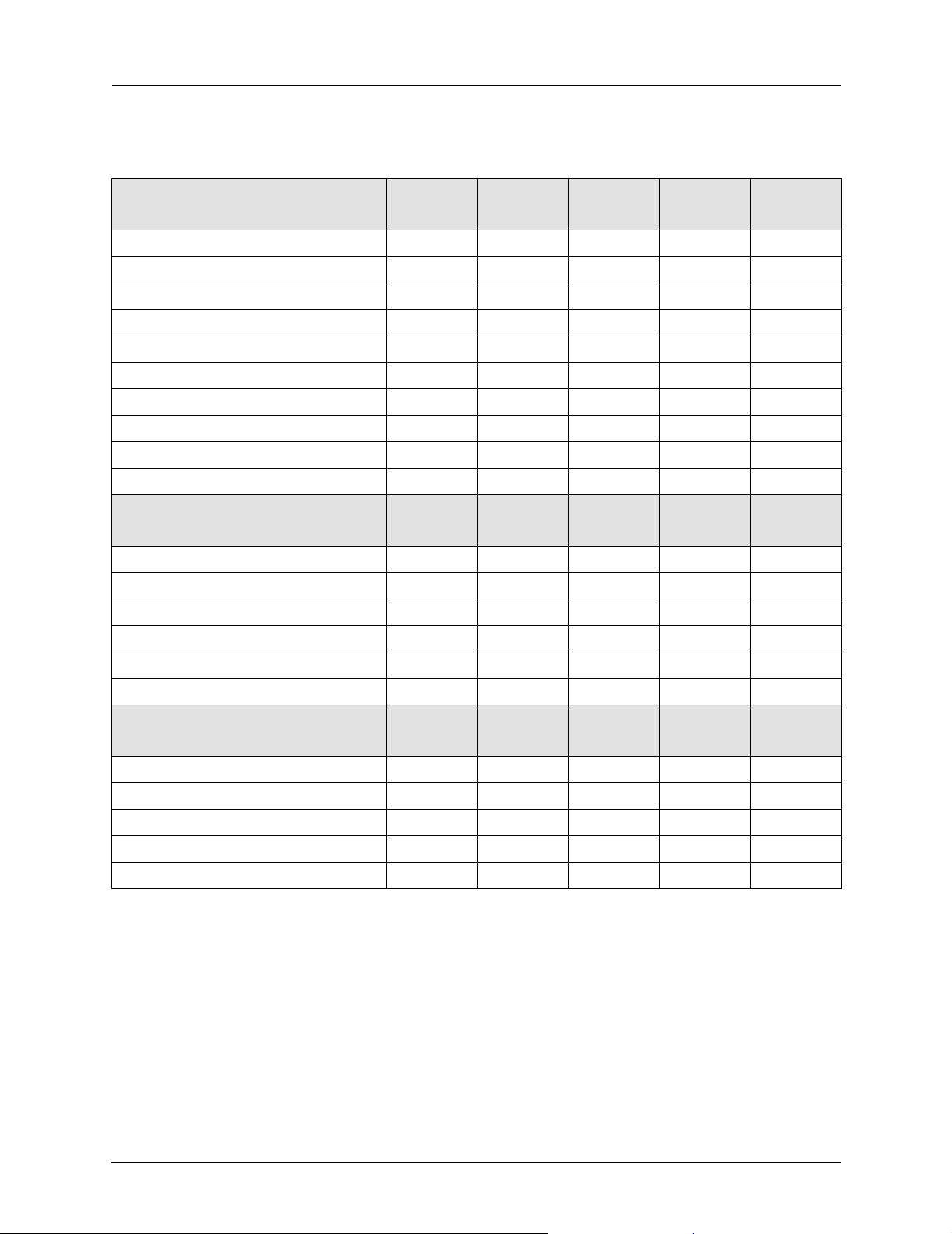
The CX23880 family is designed to be a higher quality, more flexible, and
configurable successor to the previous generation Fusion 878A. The key differences
between the Fusion 878A and the CX2388x family are summarized in Table 1-1.
The pin and software compatible nature of the CX2338x family enables a board
vendor to build a wide variety of analog and digital TV capture products from a
common code base.
The CX23880 and CX23882 are designed to enable high-functionality broadcastcentric PC cards that require high speed I/O capability. This capability is necessary to
support simultaneous compressed and uncompressed digital video/audio data flo ws in
conjunction with hardware MPEG II/MPEG IV encoders an d decoders. The CX23382
has the same feature set as the CX23880, with the exception of BTSC stereo with dbx
audio companding and VIP Host Port.
The CX23881 and CX23883 are designed to enable entry-level analog TV and stereo
broadcast PC cards. Additionally, TV channel demodulators can be connected to
enable software-based decoding of MPEG transport streams. The CX23881 has the
same feature set as the CX23882, with the exception of BTSC stereo with dbx audio
companding.
101069A Conexant 1-1
08/26/02 Preliminary Information/Conexant Proprietary and Confidential
Page 18
Product Overview CX23880/CX23881/CX23882/CX23883 Data Sheet
Table 1-1. Feature Comparison of CX2388x and Fusion 878A
Conexant PCI Decoder
Standard Features
Fusion 878A CX23881 CX23883 CX23882 CX23880
4-input CVBS ADC X X X X X
Chroma ADC (S-Video) X X X X X
NTSC/PAL/SECAM Video X X X X X
Multiple YCrCb and RGB Formats X X X X X
Notch and Comb Y/C Separation X X X X X
Serial MPEG Input Port X X X X X
S Input Port XXXXX
I
2
24-bit General Purpose I/O X X X X X
Number of DMA Channels 2 7 11 7 11
WHQL Certification X X X X X
CX2388x Family
Standard Features
Fusion 878A CX23881 CX23883 CX23882 CX23880
10-bit Video ADCs X X X X
Multi-Line 2D-Adaptive Comb Filter X X X X
High Speed Parallel MPEG Port X X X X
2
S Output Port X X X X
I
Stereo Line Out DACs X X X X
EIAJ/NICAM/A2/FM Stereo Decode X X X X
CX2388x Family
Speciality Functions
Fusion 878A CX23881 CX23883 CX23882 CX23880
BTSC with dbx Stereo Decode X X
ITU-R 656 Output Port XX
ITU-R 656 Input Port XX
Intel/Motorola Host Port (I/O) X X
VIP 2.0 Host Master Port (I/O) X
1-2 Conexant 101069A
Preliminary Information/Conexant Proprietary and Confidential 08/26/02
Page 19
CX23880/CX23881/CX23882/CX23883 Data Sheet Product Overview
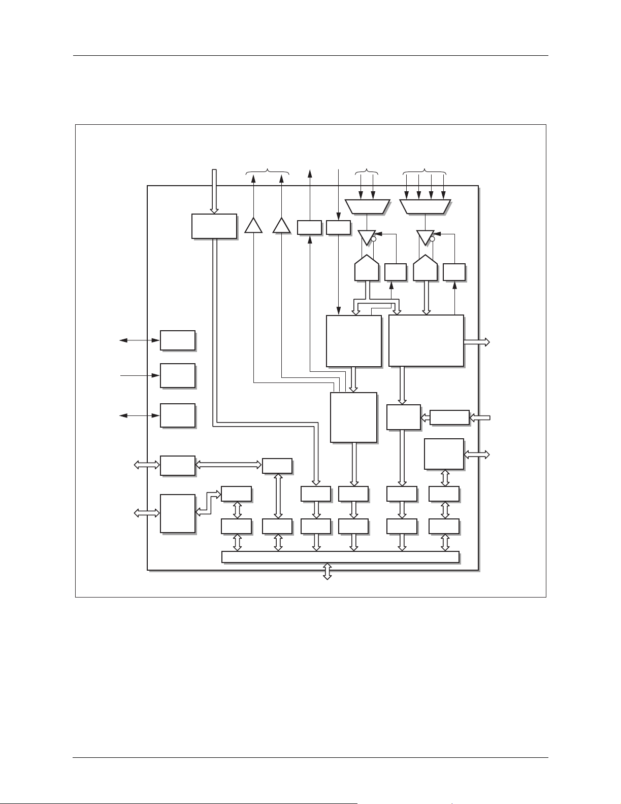
Figure 1-1 illustrates a block diagram of the CX23880.
Figure 1-1. CX23880 Detailed Block Diagram
Digital
MPEG TS/PS/ES,
Broadband Data
Broadband,
MPEG Port
Baseband
Audio
Output
Audio/
SPDIF
Output
2
Sout I2Sin
I
Digital
Audio/
S-Video/
SPDIF
Audio
Input
i/f
A/V MUX Video MUX
Composite
Video
User
Configurable
1–24 GPI/O
Available
9 MBps
Bidirectional
General
Purpose
Host Port
JTAG
Clocks
and PLL
Serial
Bus
GPI/O
16-Bit
Intel/
Motorola
Host Port
FIFO
DMA
16-Bit Audio DAC
16-Bit Audio DAC
FIFO
DMA
PCI Bus Interface
FIFO
DMA
10-Bit
ADC
Broadcast
Audio Decoder
FM, AM
NICAM/
QPSK
Audio
Control
and
Format
Conversion
FIFO
DMA
10-Bit
AGC
ADC
NTSC/PAL/SECAM
Decoder, Adaptive
Comb Filter and
Scaler
Pixel
Engine
VIP 2.0
Host Port
Interface
FIFO
DMA
Scaler
FIFO
DMA
AGC
8-Bit or 10-Bit
CCIR 656
Output
8-Bit CCIR 656
8-Bit VIP 2.0
Pixel Port
33 MBps
Bidirectional
Interface
PCI Bus
101069_052
101069A Conexant 1-3
08/26/02 Preliminary Information/Conexant Proprietary and Confidential
Page 20

Product Overview CX23880/CX23881/CX23882/CX23883 Data Sheet
1.2 Detailed Features
1.2.1 Analog Video Capture
1.2.1.1 Overview
The CX2388x integrates a 10-bit NTSC/PAL/SECAM composite and an
S-Video decoder, image resizer/scaler, Direct Memory Access (DMA) controller , and
Peripheral Component Interface (PCI) Bus master on a single device. The CX2388x
can place video data directl y into host memory for video capture appl ications and into
a target video display frame buffer for video overlay applications. As a PCI initiator,
the CX2388x can take control of the PCI bus as soon as it is available, thereby
avoid ing the need for onbo ard frame buf fers. The CX2388 x contains a pixel data First
In, First Out (FIFO) to decouple the high-speed PCI bus from the continuous video
data stream. The video data input can be scaled, color -translated, and burst-transferred
to a target location on a field basis. This allows for simultaneous preview of one field,
and capture of the other field. Alternatively, the CX2388x can capture or preview both
fields simultaneously. The fields can be interlaced into memory or sent to separate
field buffers.
1.2.1.2 Input Interface
Analog video signals are input to the CX2388x via a four-input multiplexer. The
multiplexer can select between four composite source inputs, or between three
composite and a single S-Video input source. When an S-Video source is input to the
CX2388x, the luma component is fed through the input analog multiplexer, and the
chroma component feeds directly into the C-input pin. An Automatic Gain Control
(AGC) circuit enables the CX2388x to compensate for nonstandard amplitudes in the
analog signal input.
1.2.1.3 Image Scaler
The CX2388x can reduce the video image size in both horizontal and vertical
directions independently, using arbitrarily selected scaling ratios. The X and Y
dimensions can be scaled down to one-sixteenth of the full resolution. Horizontal
scaling is implemented with a six-tap interpolation filter, while up to five-tap
interpolation is used for vertical scaling with a line store. The video image can be
arbitrarily cropped by reducing the number of active scan lines and active horizontal
pixels per line. The CX2388x supports a temporal decimation feature that reduces
video bandwidth. This is accomplished by allowing frames or fields to be dropped
from a video sequence at fixed but arbitrarily selected intervals.
1-4 Conexant 101069A
Preliminary Information/Conexant Proprietary and Confidential 08/26/02
Page 21

CX23880/CX23881/CX23882/CX23883 Data Sheet Product Overview
1.2.1.4 Reduced Instruction Set Computer Engine
The CX2388x enables separate destinations for the odd and even video fields, each
controlled by a pixel Reduced Instruction Set Comptuter (RISC) instruction list. This
instruction list is created by the CX2388x device dri ve r and can be run in the onboard
memory or host memory. The instructions control the transfer of pixels to target
memory locations on a byte resolution basis. Complex clipping can be accomplished
by the instruction list, blocking the generation of PCI bus cycles for pix els that are not
to be seen on the display.
The DMA channels can be programmed on a field basis to deliver the video data in
packed or planar format. In packed mode, YCrCb data is stored in a single continuous
block of memory. In planar mode, the YCrCb data is separated into three streams
which are burst to different target memory blocks. Having the video data in planar
format is useful for applications where the data compression is accomplished via
software and the CPU.
1.2.1.5 UltraLock™
The CX2388x employs a proprietary technique known as UltraLock to lock to the
incoming analog video signal. It always generates the required number of pixels per
line from an analog source in which line length can vary by as much as a few
microseconds. UltraLock’s digital locking circuitry enables the CX2388x to lock onto
video signals quickly and accura tel y, regardless of their source. Because the t echnique
is completely digital, UltraLock can recognize unstable signals caused b y VC R head
switches or any ot her de viation and adapt the locking mechanism to accommodate the
source. UltraLock uses nonlinear techniques that are difficult, if not impossible, to
implement in genlock systems. And, unlike linear techniques, it adapts the locking
mechanism automatically.
1.2.1.6 Vertical Blanking Interval (VBI) Data Capture
The CX2388x provides a flexible solution for capturing and decoding disparate VBI
data types such as closed caption data, teletext, Vertical Internal Time and Control
(VITC) codes, HTML data, or multicast data. The CX2388x can operate in a VBI
Line Output mode, in which the VBI data is only captured during selected lines. This
mode of operation enables concurrent capture of VBI lines containing ancillary data
and normal video image data. In addition, the CX2388x supports a VBI Frame Output
mode in which every line in the video frame is treated as if it were a VBI line. This
mode of operation is designed for use with still-frame capture and processing
applications where sophisticated image decoding can be performed in the software
domain.
1.2.1.7 Macrovision Detector
With the advent of powerful Central Processing Units (CPUs) that enable softwarebased video compression, low-cost hardware MPEG encoders, cheap and rewritable
storage media, and pervasive broadband communications, original content protection
is paramount. To this end, the CX2388x fully implements Macrovision 7.01. When an
end user attempts to connect a Digital Video Disk (DVD) player, a digital satellite/
cable decoder’s composite, or S-Video outputs to the input of a CX2388x-based PCI
card , t he Macrovision pulses, signals are detected, and a bit is set . It is up to the board
vendor to read the bit and determine what action will be taken.
101069A Conexant 1-5
08/26/02 Preliminary Information/Conexant Proprietary and Confidential
Page 22

Product Overview CX23880/CX23881/CX23882/CX23883 Data Sheet
1.2.2 Analog Audio Capture
The CX2388x captures and decodes all major terrestrial broadcast audio standards.
The CX2388x digitizes and oversamples the low Intermediate Frequency (IF) signal
from a Television (TV) tuner, and extracts and decodes the broadcast audio signal.
The decoded audio is sample rate converted to a 48 kHz Pulse Code Modulation
(PCM) stereo signal to simplify processing and interfacing. This 48 kHz stream can
be routed to the built-in +85 dB Signal-to-Noise Ratio (SNR) stereo audio Digital-toAnalog Con verters (D A Cs) for connection to the PC’s sound card or headphones, to an
external digital-audio interface, or to the PCI bus and host for direct capture by a
software audio codec.
If capture of line-level stereo audio signals is required, an inexpensive audio Analogto-Digital Conv erter (ADC) can be directl y connected to the CX2388x’s I
and controlled via the serial bus master.
2
S input port
1.2.3 ITU-R 656 4:2:2 Data Output
The CX23880/CX23882 provides a 27-MHz, 8- or 10-bit ITU-R 656 decoded video
output interface to allow connection of a third-party MPEG II encoder or other type of
video codec. This is useful when the host CPU is not powerful enough to perform
such tasks in software, or when high-quality encoding must be achieved. Please
contact Conexant Application Engineering for a list of supported third-party video
compressors.
1.2.4 ITU-R 656/VIP 2.0 Pixel Data Input
The CX23880/CX23882 provides a 27-MHz, 8-bit ITU-R 656 decoded video input
interface to allow a third-party MPEG II decoder or codec to send 4:2:2 data over the
PCI bus to a target video display frame buffer for video overlay. Alternatively, 480line progressive scan video from the CX23490 All-Format MPEG II decoder can be
input to this port using Video Interface P ort (VIP) 2.0-compliant pixel timing at up to
54 MHz.
1.2.5 MPEG Data Port
Channel demodulators used for digital television or broadband data applications over
terrestrial, satellite, or cable networks can be directly connected to the CX2388x’s
MPEG data port to deliv er transport streams to the host for subseq uent sto rage to disk
or software decode. Either parallel, common-interface Digital Video Broadcasting
(DVB) or serial data paths from the channel demodulator can be supported at data
transfer rates of up to 80 Mbps. If the Serial Interface mode is used, the remaining
unused pins on this port can be allocated as General Purp ose Input/Output (GPIO).
1-6 Conexant 101069A
Preliminary Information/Conexant Proprietary and Confidential 08/26/02
Page 23

CX23880/CX23881/CX23882/CX23883 Data Sheet Product Overview
1.2.6 VIP 2.0 Host-Master Interface Port (CX23880)
The VIP 2.0 Host-Master interface allows the CX23880 to communicate with all
devices that are compliant with the VIP slave specification. This implementation of a
VIP 2.0 master is backward-compatible with all VIP 1.1-compliant slave interfaces.
The CX23880 is designed to connect to the CX23490 All-F ormat MPEG II decoder
via this interface.
The functionality of the VIP Host Master Interface is threefold. The first concept is to
stream data from a VIP slave into host memory via the PCI bus. The second concept is
to stream out data to a VIP slave that is sent over the PCI bus by the host. The third
concept is for the host to be able to access register space on connected VIP slave
devices.
1.2.7 General Purpose Host Interface Port (CX23880/CX23882)
The General Purpose Host interface allows the connection of moderate-to-relatively
slow speed third party peripherals such as infrared remote control processors, codec
host ports, smart card controllers, etc., to the CX23880/CX23882. This port allows
simultaneous connection to two peripherals gluelessly, or as many as four peripherals
with the use of external glue logi c to pro vide the addi tional chip selects. This interface
can have one upstream and one downstream DMA channel active to or from the
external peripherals at any given time. Data bursting is not supported.
1.2.8 GPIO Port
The CX2388x provides up to 24 GPIO pins. These GPIO pins are shared with the
following pins/ports groups so that the user can determine exactly which pins can be
dedicated to specific functions versus general purpose I/O functions.
1. MPEG Parallel Data Port
2. ITU–R 656 4:2:2 Data Output
3. ITU–R 656 4:2:2 Data Input
4. Extended VIP Host Port
5. Extended General Purpose Host Port
1.2.9 Serial Bus Interface
The CX2388x’s serial bus interface supports both 99.2 kHz timing transactions and
396.8 kHz, repeated start, multibyte sequential transactions. As a serial bus master,
CX23880/CX23881 can program other devices on the video card, such as a TV tuner,
as long as the device address is known. The CX2388x supports multibyte sequential
reads (more than one transaction) and multibyte write transactions (greater than three
transactions), which enable communication to devices that support auto-incremental
internal addressin g.
101069A Conexant 1-7
08/26/02 Preliminary Information/Conexant Proprietary and Confidential
Page 24

Product Overview CX23880/CX23881/CX23882/CX23883 Data Sheet
1.2.10 PCI Bus Interface
The CX2388x is designed to efficiently utilize the available 132 MBps PCI bus. The
32-bit dwords are output on the PCI bus with the appropriate image data under the
control of the DMA channels. The video stream consumes bus bandwidth with
average data rates va rying from 44 MBps for full-size 768 × 576 PAL RGB32, to 4.6
MBps for NTSC CIF 320 × 240 RGB16, to 0.14 MBps for NTSC ICON 80 × 60 8-bit
mode.
The pixel instruction stream for the DMA channels consumes a minimum of
0.1 MBps. The CX2388x provides the means for mitigating the bandwidth
bottlenecks caused by slow targets and long bus access latencies that can occur in
some system configurations. To overcome these system bottlenecks, the CX2388x
gracefully degrades and recov ers from FIFO overruns to the nearest pixel in real-time.
1-8 Conexant 101069A
Preliminary Information/Conexant Proprietary and Confidential 08/26/02
Page 25
CX23880/CX23881/CX23882/CX23883 Data Sheet Product Overview
1.3 Pin Descriptions
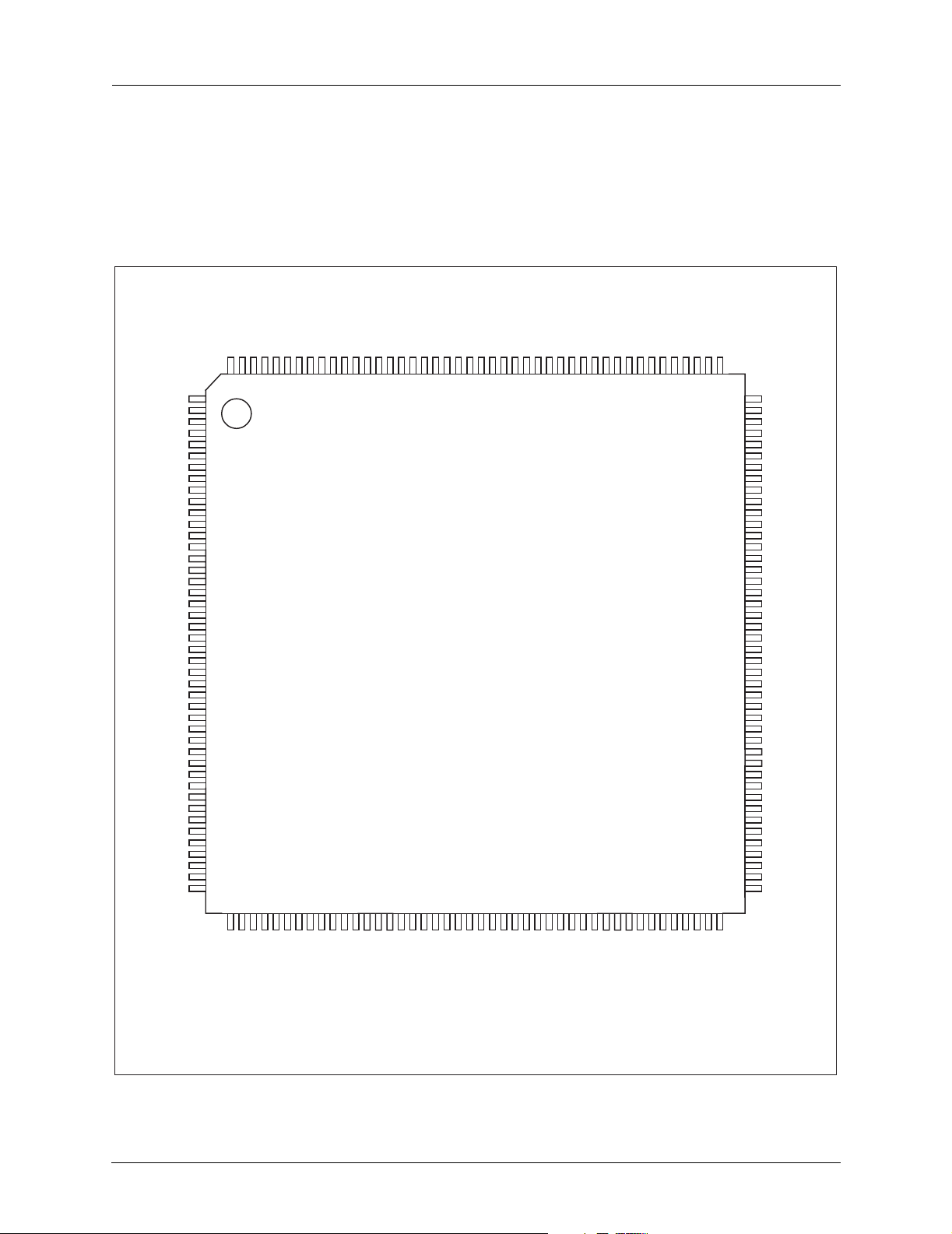
Figure 1-2 displays the CX23880 Pinout diagram. Table 1-2 provides a description of
pin functions grouped by common function.
Figure 1-2. CX23880 Pinout Diagram
TSCLK
TSVAL/ERR
TSSOP
TSDAT[0]
VDDIO
V
GND
G
PIO[23]
G
PIO[22]
G
PIO[21]
PIO[20]
G
G
PIO[19]
G
PIO[18]
G
PIO[17]
G
PIO[16]
V
HAD[1]
HAD[0]
V
V
HCTL
VIRQ#
VIPCLK
INTA#
R
ST#
EQ#
R
NT#
G
VDDIO
VDD
GND
AD[31]
A
D[30]
A
D[29]
D[28]
A
D[27]
A
AD[26]
D[25]
A
D[24]
A
BE[3]#
C
I
DSEL
AD[23]
D[22]
A
A
D[21]
A
D[20]
AD[19]
A
D[18]
G
#
RSTO
174
173
172
171
_
YS
S
170
TCKT
169
MS
168
DI
T
167
SCKO
LRCKOADATOASCKIALRCKIADATI
A
A
175
176
1
2
3
4
5
DD
6
7
8
9
10
11
12
13
14
15
16
17
18
19
20
21
22
23
24
25
26
27
28
29
30
31
32
33
34
35
36
37
38
39
40
41
42
43
ND
44
45464748495051525354555657585960616263646566676869707172737475767778798081828384858687
2
PP
GNDAGDA
V
P
164
165
166
1
REF
_
WM
ACSO
L
P
162
163
2
REF
_
WM
P
161
ASCO
ADA
V
R
159
160
DO
_T
REFX
I
158
CR
2
AA
V
157
2
CM
V
156
2
REFP
V
155
2
REFN
V
154
CR
2
GA
BGOUT
A
V
152
153
INIFAVINC
V
151
150
GND
V
149
GASH
A
148
AASH
V
147
SUB
A
146
1
MUX
V
145
2
MUX
V
144
3
MUX
V
143
4
MUX
V
142
CR
1
GA
A
141
1
REFN
V
140
1
REFP
V
139
1
CM
V
138
CR
1
AA
V
137
GXTL
A
136
1
T
X
135
2
T
X
134
AXTL
V
133
132
131
130
129
128
127
126
125
124
123
122
121
120
119
118
117
116
115
114
113
112
111
110
109
108
107
106
105
104
103
102
101
100
99
98
97
96
95
94
93
92
91
90
89
88
SDA
S
CL
PIO[0]
G
PIO[1]
G
G
PIO[2]
PIO[3]
G
PIO[4]
G
G
PIO[5]
PIO[6]
G
PIO[7]
G
GPCLKI
VDDIO
ND
G
G
PIO[8]
PIO[9]
G
PIO[10]
G
G
PIO[11]
PIO[12]
G
PIO[13]
G
PIO[14]
G
GPIO[15]
G
PCLKO
AD[0]
H
AD[1]
H
AD[2]
H
H
AD[3]
AD[4]
H
VPP1
PGND
VDD
VDDIO
AD[5]
H
AD[6]
H
H
AD[7]
H
AD[8]
AD[9]
H
AD[10]
H
H
AD[11]
AD[12]
H
H
AD[13]
H
AD[14]
AD[15]
H
CS#
H
HRD/HDS#
#
#
#
#
#
[17]
D
A
[16]
D
A
#
[2]#
RDY
I
BE
RAME
F
C
IO
DD
V
V
DDIO
V
RDY
T
TOP
S
EVSEL
D
ERR
P
#
ERR
S
#
#
IO
AR
P
LK
ND
[14]
D
A
[13]
D
A
DD
C
V
G
DDIO
V
[1]#
[15]
D
BE
A
C
[9]
[8]
[7]
[6]
[5]
[4]
[3]
[2]
[1]
[0]
ND
V
[12]
[11]
[10]
[0]#
D
D
D
D
D
D
D
D
D
A
A
A
A
BE
A
C
D
A
A
A
A
A
DD
D
D
D
V
G
A
A
A
#
DDIO
EXFB
ALE
RDY
HRW
V
/
H
H
H
WR
H
VDD: 1.8 V digital core supply
Vpp,Pgnd: 1.8 V PLLs supply, return
Vddio: 3.3 V digital I/O supply
Gnd: Digital core, I/O return supply
VIO: PCI 5 V diode clamp supply
101069_002
101069A Conexant 1-9
08/26/02 Preliminary Information/Conexant Proprietary and Confidential
Page 26

Product Overview CX23880/CX23881/CX23882/CX23883 Data Sheet
Table 1-2. Pin Descriptions Grouped by Pin Function (1 of 5)
Pin Number Pin Name Dir Type Signal Description
PCI Interface (50 Pins)
63 CLK I — Clock All PCI signals except RST# and INT A #
are sampled on the rising edge of this
33.3333 MHz clock.
22 RST# I — Reset Bus reset causes all PCI outputs to
asynchronously three-state.
23 REQ# O t/s Request Agent requests bus
24 GNT# I — Grant Agent granted bus
37 IDSEL I — Initialization Device
Select
[28–35, 38–43,
AD[31:0] I/O t/s Address/Data Address phase when FRAME# is 1st
48, 49, 60–62,
68–72, 74–81]
[36, 50, 59, 73] CBE[3:0]# I/O t/s Bus Command/
Byte Enables
Selects device during configuration read
and write transactions.
asserted, and data transfer when IRDY#
and TRDY# are both asserted.
Bus transaction-type command during
address phase, and byte enables during
entire data phase.
58 P AR I/O t/s Parity Even parity across {AD, C/BE#}, lags
address/data phase
51 FRAME# I/O s/t/s Cycle Frame Asserted to begin bus transaction.
Deasserted when transaction in final data
phase.
52 IRDY# I/O s/t/s Initiator Ready Indicates the Initiator is ready to accept
read data or has placed valid write data
on the AD.
53 TRDY# I/O s/t/s Target Ready Indicates the Target is ready to accept
write data or has presented valid data on
AD during a read.
54 DEVSEL# I/O s/t/s Device Select Indicates the driving device has decoded
the address as the target of the current
access.
55 STOP# I/O s/t/s Stop Target requesting master to stop current
transaction
56 PERR# I/O s/t/s Parity Error Report data parity error
57 SERR# O t/ s System Error Report address parity or system error
21 INTA# O t/s Interrupt A Request an interrupt
JTAG Signals (4 Pins)
169 TCK I — Test Clock Used to synchronize all JTAG test
structures. Tie low when not using
JTAG.
1-10 Conexant 101069A
Preliminary Information/Conexant Proprietary and Confidential 08/26/02
Page 27

CX23880/CX23881/CX23882/CX23883 Data Sheet Product Overview
Table 1-2. Pin Descriptions Grouped by Pin Function (2 of 5)
Pin Number Pin Name Dir Type Signal Description
168 TMS I r T es t Mode Select T ransitions drive JT A G st ate machine
sequence. Tie high or leave floating when
not using JTAG. A fixed sequence on this
pin initializes the JTAG tap controller.
167 TDI I r Test Data In Load input instructions and /or test vector
data for boundary scan and internal scan.
Tie high or leave floating when not using
JTAG.
158 IREFX—TDO O Test Data Ou t Output for verifying JTAG serial
operations. The output is 3-stated when
not using JTAG port.
VIP 2.0 Host Master Signals (5 or 11 Pins)
16, 17
8–15
VHAD[1:0]
GPIO[23:16]
(1)
I/O — VIP Host Address/
Data
VIP Address and Data bus, defaults to
VIP1.1 interface with 2 addr/data pins.
Can be configured as VIP 2.0 with 8 addr/
data pins (GPIO).
18 VHCTL I/O — VIP Host Control VIP System Host control
19 VIRQ# I/O od VIP Interrupt
VIP Interrupt Request (open drain)
Request
20 VIPCLK O — VIP Clock VIP master output clock. This clock is
buffered. PCI CLK = 33.3333 MHz
Transport Stream Signals (4 or 11 Pins)
4
TSDAT[0]
3 TSSOP I — Transport Stream
(2)
I — Transport Stream
Data
Start of Packet
Transport Stream Input data bus.
TSDAT[0] is used in serial mode.
Tr ansport Stream Start-of-Packet
indicator. Indicates first byte in serial or
parallel transport packet.
2 TSVAL/ERR I — Transport Stream
Transport Stream Error or Valid indicator
Error/Valid
1 TSCLK I — Transport Stream
Clock
Transport Stream input clock. All other
transport stream inputs are sampled on
the rising (falling) edge of TSCLK
Host Master Signals (22 Pins)
[91–101, 106–
110]
90 HCS# O — General Purpose
HAD[15:0] I/O — General Purpose
Host Address/Data
Bidirectional address/data access bus
External chip select
Host Chip Select
89 HRD#/
HDS#
O — General Purpose
Host Read/Data
Either the active-low read signal or the
programmable polarity data strobe signal
Strobe
101069A Conexant 1-11
08/26/02 Preliminary Information/Conexant Proprietary and Confidential
Page 28

Product Overview CX23880/CX23881/CX23882/CX23883 Data Sheet
Table 1-2. Pin Descriptions Grouped by Pin Function (3 of 5)
Pin Number Pin Name Dir Type Signal Description
88 HALE# O — General Purpose
Host Address Latch
Address Latch Enable signal, used only in
multiplexed 16-bit address/data mode
Enable
87 HWR/
HRW#
O — General Purpose
Host Write/Read,
Either the active-low write signal or the
read/write bar
not Write
86 HRDY# I r General Purpose
External data transfer acknowledge signal
Host Ready
85 HEXFB I r General Purpose
Host External
Status
Handshaking signal for use in DMA mode
to indicate the status of the external
source or destination FIFO.
GPIO/Serial Bus/Reset (29 Pins)
[8–15, 112–119,
123–130]
122 GPCLKI I I General Purpose
GPIO[23:0] I/O I/O General Purpose
Input/Output
See GPIO Cross-Reference Table
Digital Video Input Reference clock
Input Clock
111 GPCLKO O O General Purpose
Digital Video Output Reference clock
Output Clock
132 SDA I/O od Serial Data Bit data or acknowledge
131 SCL I/O od Serial Clock Bit clock
170 SYS_RSTO# O t/s System Reset Out Logical PCI reset, soft reset, or power-on
reset output. This is used to reset
CX23880’s peripheral under software
control or with hard reset.
Digital Audio (6 Pins)
171 ADATI I r Audio Data In Bit Serial Input data
172 ALRCKI I r Audio Left/Right
Left/Right Framing Input clock
Clock In
173 ASCKI I r Audio Serial Clock
Bit Serial Input clock
Input
174 ADATO O r Audio Data Out Bit Serial Output data
175 ALRCKO O r Audio Left/Right
Left/Right Framing Output clock
Clock Out
176 ASCKO O r Audio Serial Clock
Bit Serial Output clock
Output
Crystal Interface Signals (4 Pins)
134 XT2 O — XT2 Crystal oscillator input pin
135 XT1 I — XT1 Crystal oscillator or clock oscillator
input pin can be connected to XT1.
1-12 Conexant 101069A
Preliminary Information/Conexant Proprietary and Confidential 08/26/02
Page 29

CX23880/CX23881/CX23882/CX23883 Data Sheet Product Overview
Table 1-2. Pin Descriptions Grouped by Pin Function (4 of 5)
Pin Number Pin Name Dir Type Signal Description
133 VAXTL — — PSUP_XTAL XTAL and Sample and Hold digital
136 AGXTL — — NSPU_XTAL
power/ground. Nominal VA = 3.3 V
ADC Interface (23 Pins)
[145:142] VMUX[1:4] I A Video Mux {1:4} Analog composite video inputs to the
on-chip 4:1 analog multiplexer. Unused
inputs should be tied to AGA1.
150
151
VINC
VINIFA
I A Chroma baseband
vid: Audio low IF
Analog chroma input to the C-A/D,
multiplexed with Audio IF input from the
tuner. Unused inp ut should be tied to
AGA2.
138
156
140
154
139
155
VCM1
VCM2
VREFN1
VREFN2
VREFP1
VREFP2
O A VCM_ADC{1:2} Common mode voltage referenc e
O A VREFN{1:2} Input Negative reference (1.0 V)—one
for each Y and C/Aud ADCs, cap to AGA.
O A VREFP{1:2} Input Positive reference (1.8 V)—one
for each Y and C/Aud ADCs, cap to AGA.
153 VBGOUT O A VBGOUT Voltage reference 1.21 V nominal, cap to
AGA
137, 157 VAA{1:2}CR — A VAA{1:2}CR A/D core power/ground. Nominal
141, 152 AGA{1:2}CR — A AGA{1:2}CR
VA = 3.3 V
146 ASUB — — ASUB A/D core substrate (ground)
147 VAASH — — PSUPA_SHA_ADC A/D Sample and Hold Analog power/
148 AGASH — — NSUPA_SHA_ADC
ground. Nominal VA = 3.3 V
149 VGND I A/D Virtual Ground Single-end-to-differential converter
input for common-mode noise rejection.
Connect to analog ground via 3.3 µF
series capacitor.
105, 165 VPP1/VPP2 — — VPP1, VPP2 PLL power supply. VD= 1.8 V
104, 166 PGND — — PGND PLL return supply
158 IREFX_TDO I/O A/D IREF_EXT/TDO Shared analog current ref pin JTAG TDO
pin
Audio Output DAC Signals (6 Pins)
159 VADA — — VADA DAC analog core power and ground.
164 AGDA — — AGDA
VA = 3.3 V
163 LASCO O A LASCO DAC Pulse Width Modulator (PWM), left
stereo audio output channel
160 RASCO O A RASCO DAC PWM, right stereo audio output
channel
161 PWM_REF2 O A PWM_REF2 Audio DAC reference, right
162 PWM_REF1 O A PWM_REF1 Audio DAC reference, left
101069A Conexant 1-13
08/26/02 Preliminary Information/Conexant Proprietary and Confidential
Page 30
Product Overview CX23880/CX23881/CX23882/CX23883 Data Sheet
Table 1-2. Pin Descriptions Grouped by Pin Function (5 of 5)
Pin Number Pin Name Dir Type Signal Description
I/O and Core Power and Ground (23 Pins)
6, 26, 45, 65,
83, 103
7, 27, 44, 64,
VDD — — VDD Digital core power supply. Nominal
VDD = 1.8 V
GND — — GND Ground for digital core (GND)
82, 120
5, 25, 46, 66,
84, 102, 121
VDDIO — — VDDI and VDDO Digital inputs/outputs power supply.
VD = 3.3 V
47, 67 VIO — — VIO +5 V reference for 5 V-tolerant PCI input
buffers
Note(s):
(1)
VHAD[1:0] is the default for the 5-pin VIP Host Port setting.
(2)
TSDAT[0] is the default for the 4-pin serial MPEG Data Port setting. The 11-pin setting shares GPIO pins.
3. Type: r active resistive pull-up
od open-drain
t/s three-state
s/t/s sustained three-state
[x:y] Bus
{u:v} Array of signal ports—expand to number without braces.
4. All signal I/O are LVTTL compatible (3.3 V operation with 3.9 V tolerance), except for the PC I signals whic h are all 5 .5 V tolerant.
5. All inputs are Schmitt unless otherwise noted. The PCI inputs do not have hysteresis.
6. All outputs have drive capability I
= 4 mA unless otherwise noted.
OL
1-14 Conexant 101069A
Preliminary Information/Conexant Proprietary and Confidential 08/26/02
Page 31

2
Functional Description
2.1 Audio Decoder
This section of the data sheet describes the fu nctionality of t he analo g broadc ast audio
decoder in logical sequence from the audio input at the anal og front end, to the output
of digital audio samples to the PCI bus or to the on-board stereo DACs.
2.1.1 Overview
The CX2388x’s audio subsystem pro vides hardw are-based demodulatio n for all major
terrestrial broadcast audio standards used world-wide.
Decoded broadcast audio can be output directly to the on-board stereo DACs for
connection to the PC’s sound card, to I
interfaces, or to the host via the PCI bus for software-based playback or encoding.
The major functional blocks of the audio subsystem are illustrated in Figure 2-1 and
are broken down into the following se cti ons:
2
S for high-fidelity digital coaxial and optical
! Analog Front End (AFE) and Chroma-ADC (C-ADC)
! Multistandard audio demodulator
! Broadcast audio standard selection
! Audio PLL initialization
! Input Source Select
! Dematrix Control
! Audio control and Sample Rate Converter
2
! I
S input and output
! Audio DACs
101069A Conexant 2-1
08/26/02 Preliminary Information/Conexant Proprietary and Confidential
Page 32
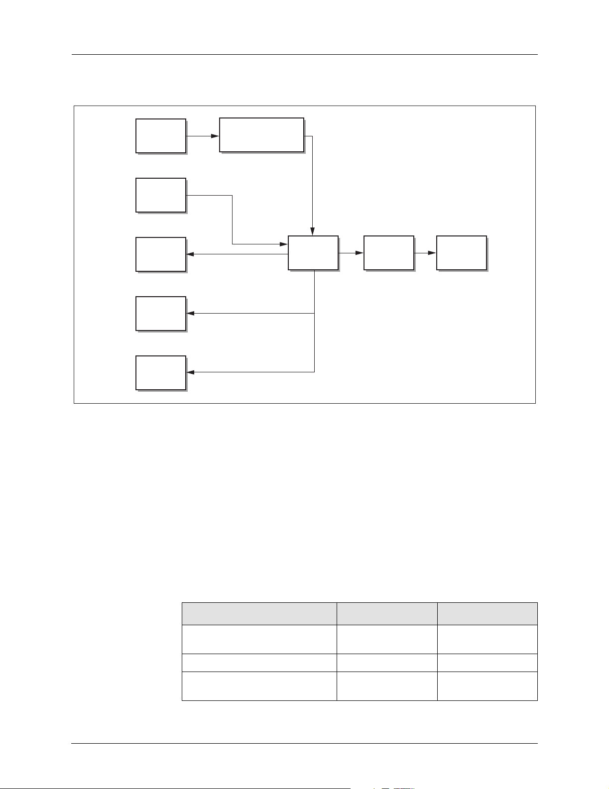
Functional Description CX23880/CX23881/CX23882/CX23883 Data Sheet
Figure 2-1. Simplified Block Diagram of CX2388x Audio Subsystem
Chroma
ADC
2
I
S In
2
S Out
I
Left
DAC
Right
DAC
FM/AM/NICAM/QPSK
Demodulation
Audio
Control
Audio
FIFO
DMA
101069_014
2.1.2 Analog Front End (AFE) and Chroma-ADC (C-ADC)
The CX2388x has a dedicated input pin, VINIF A (pin 151), that is used as the input to
the C-ADC for sampling low-IF audio signals from a television/FM tuner. This pin is
multiplexed with input pin VINC (pin 150) for access to the C-ADC.
Recognizing that broadcast video sources are composite video only, the 10-bit C-ADC
is shared between the low-IF broadcast audio signal and the chroma portion of a
baseband S-Video signal (Y, C). As broadcast video and S-Video are mutually
exclusive, the CX2388x takes advantage of this fact to utilize the C-ADC to capture
broadcast audio signals.
See Table 2-1 for the CX2388x ADC assignments.
Table 2-1. ADC Assignments
Application ADC 1/-1 ADC 2/C
Capture composite video from a video
camcorder
Capture S-Video from a video camcorder Y-signal digitization C-signal digitization
Capture composite video and broadcast
audio from a TV tuner
Composite signal
digitization
Composite signal
digitization
—
Low IF signal digitization
2-2 Conexant 101069A
Preliminary Information/Conexant Proprietary and Confidential 08/26/02
Page 33
CX23880/CX23881/CX23882/CX23883 Data Sheet Functional Description
T o enable the C-ADC for broadcast audio sources, the CX2388x must be programmed
appropriately for composite/broadcast audio sources versus S-Video sources. Bit [0]
of the AFE_CFG_IO register (location 24’h35C04C) is used to configure the C-ADC
for either a broadcast audio signal or a chroma video signal.
24’h35C04C—AFE_CFG_IO Register
Bits Type Default Name Description
[0] RW 1'b0 V_A_Mode 0 = selects audio mode
1 = selects video mode
See Chapter 3 for details of the external circuit required to connect the audio output of
a television/FM tuner to the CX2388x.
2.1.2.1 Selecting Optional Gain Stage
The low-IF audio signal from a television/FM tuner is nominally 120 mV
amplitude. For best performance, the C-ADC, when configured to capture broadcast
audio, expects a 1.0 V
input signal.
RMS
For nominal low-IF audio signals, an optional +12 dB gain stage should be enabled to
provide optimal signal amplitude to the C-ADC for maximum ADC performance.
24’h320628—AFE_12DB_EN Register
Bits Type Default Name Description
[0] RW 1'b0 AFE_12DB_EN Enable +12 dB gain at AFE
[15:1] RO 15'h0000 — Reserved
RMS
101069A Conexant 2-3
08/26/02 Preliminary Information/Conexant Proprietary and Confidential
Page 34

Functional Description CX23880/CX23881/CX23882/CX23883 Data Sheet
2.1.3 Multistandard Audio Demodulator
The CX23880 supports the broadcast audio standards listed in Table 2-2.
Table 2-2. Supported Broadcast Audio Standards
Table 2-3. BTSC (FM/AM/FM)
Broadcast System
NTSC (M) 4.5 BTSC-Stereo + SAP USA, Canada, Mexico,
NTSC (M) 4.5 FM-FM (EIAJ) Japan
NTSC (M) 4.5/4.724212 FM-Stereo (A2) Korea
PAL (B) 5.5/5.7421875 FM-Stereo (A2) Germany
PAL (D) 6.5/5.85 FM-Mono/NICAM China
PAL (G) 5.5/5.85 FM-Mono/NICAM Scandinavia, Spain
PAL (I) 6.0/6.552 FM-Mono/NICAM UK, Hong Kong
SECAM (K) 6.5/6.2578125 FM-Stereo East Europe
SECAM (L) 6.552/5.85 AM-Mono/NICAM France
FM-Radio 10.7 FM Stereo Radio Various
Sound Carrier
Frequency (MHz)
Modulation Country
Taiwan
The specifications of the supported broadcast audio standards are listed Tables 2-3
through 2-8.
Parameter Description Stereo SAP Unit
S/N Signal-to-Noise 60 55 dB
THD Total Harmonic Distortion + Noise 0.1 0.1 %
BW
audio
XTALK Crosstalk 70 70 dB
Separation Stereo Separation 30 N/A dB
IF Audio 2
F
sub
Modulation Modulation Type L+R: FM, 25
Emphasis Emphasis Applied L+R: 75us
Pilot Subcarrier Pilot Tone @ 15734 kHz —
Audio Bandwidth 50–15k 50–10k Hz
nd
IF, Block FM 4.50000 MHz
Subcarrier Frequency L+R: None
L-R: 31468
kHz deviation
L-R: AM, dual
sideband,
suppressed
carrier
L-R: dbx
78670 Hz
FM: 10 kHz
deviation
dbx —
—
2-4 Conexant 101069A
Preliminary Information/Conexant Proprietary and Confidential 08/26/02
Page 35
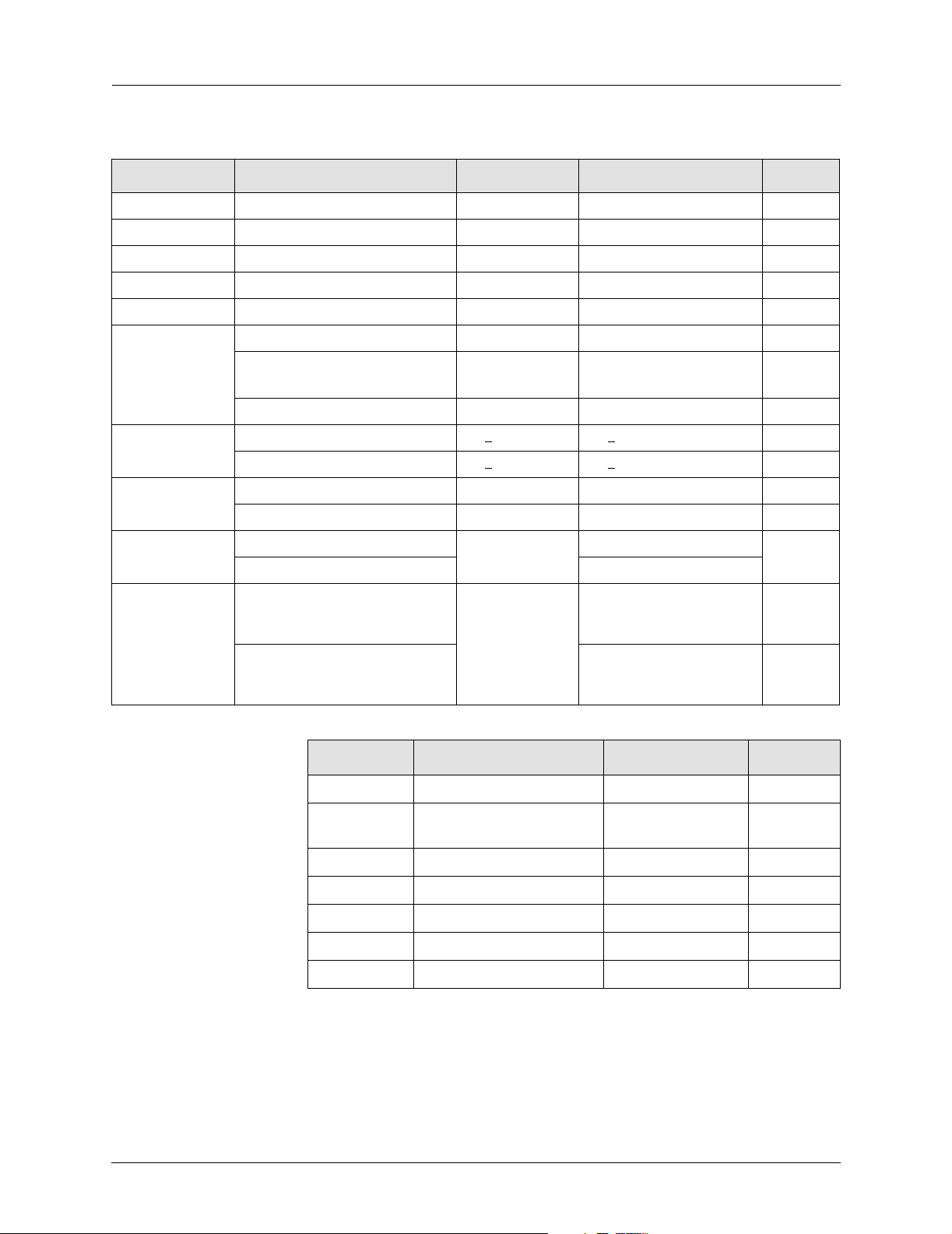
CX23880/CX23881/CX23882/CX23883 Data Sheet Functional Description
Table 2-4. A2 (FM/FM)
Parameter Description Mono Stereo Unit
S/N Signal-to-Noise 55 55 dB
THD Total Harmonic Distortion + Noise 0.1 0.1 %
BW
audio
Audio Bandwidth 40–15k 40–15k Hz
XTALK Crosstalk — 70 dB
Separation Stereo Separation — 40 dB
nd
IF Audio 2
Audio 2
IF (B/G) 5.5 5.7421875 MHz
nd
IF (D/K) 6.5 6.2578125
MHz
6.7421875
nd
Audio 2
IF (M) 4.5 4.724212 MHz
Modulation Modulation Type (B/G/D/K) FM: +
Modulation Type (M) FM: +
50 kHz FM: +50 kHz —
25 kHz FM: +25 kHz —
Emphasis Emphasis Applied (B/G/D/K) 50 50 —
Emphasis Applied (M) 75 75 —
Content Content of Signal (B/G/D/K) ( L+R)/2 R —
Content of Signal (M) (L-R)/2
Pilot Subcarrier Pilot (B/G/D/K) None 50% AM carrier at 54.6875 kHz
—
with tone at 117.5 Hz (Stereo)
274.1 Hz (dual)
Subcarrier Pilot (M) 50% AM carrier at 55.0699 kHz
—
with tone at 149.9 Hz (Stereo)
276.0 Hz (dual)
Table 2-5. System L (AM Mono)
Parameter Description Mono Unit
S/N Signal-to-Noise 40 dB
THD Total Harmonic Distortion +
0.1 %
Noise
BW
audio
Audio Bandwidth 40–15k Hz
XTALK Crosstalk — dB
IF Audio 2
nd
IF, Block FM 6.5 MHz
Modulation AM 54 %
Emphasis Emphasis Applied — —
101069A Conexant 2-5
08/26/02 Preliminary Information/Conexant Proprietary and Confidential
Page 36
Functional Description CX23880/CX23881/CX23882/CX23883 Data Sheet
Table 2-6. EIA-J (FM/FM)
Parameter Description L+R L-R Unit
S/N Signal-to-Noise 60 60 dB
THD Total Harmonic Distortion +
0.1 0.1 %
Noise
BW
audio
Audio Bandwidth 50–15k 50–15k Hz
XTALK Crosstalk 70 70 dB
Separation Stereo Separation 30 dB
IF Audio 2
F
sub
Modulation Modulation Type FM: 25 kHz
nd
IF, Block FM 4.500000 MHz
Subcarrier Frequency None 31468 Hz
FM: 20 kHz
deviation
deviation
Emphasis Emphasis Applied 75 75 µs
Delay Transmitter-sided Delay 20 0 µs
Pilot Subcarrier Pilot 60% AM at 55069 kHz,
unmodulated if Mono,
982.5 Hz if Stereo, 922.5
Hz if bilingual
Table 2-7. FM Radio (FM/AM)
Parameter Description L+R L-R Unit
S/N Signal-to-Noise 65 dB
—
—
THD Total Harmonic Distortion +
0.1 %
Noise
BW
audio
Audio Bandwidth 20–19k Hz
Separation Stereo Separation 40 dB
IF Audio 2
F
sub
Modulation Modulation Type FM: 75 kHz
nd
IF, Block FM 10.70000 MHz
Subcarrier Frequency None 38000 Hz
deviations
AM: double
sideband,
—
suppressed
carrier
Emphasis Emphasis Applied (US) 75 75 µs
Emphasis Applied (Europe) 50 50 µs
Pilot Subcarrier Pilot 19 kHz FM —
RDS RDS Output Data Stream 38 kHz, 16-bit I/Q —
2-6 Conexant 101069A
Preliminary Information/Conexant Proprietary and Confidential 08/26/02
Page 37
CX23880/CX23881/CX23882/CX23883 Data Sheet Functional Description
Table 2-8. NICAM (DQPSK)
Parameter Description Stereo Unit
S/N Signal-to-Noise 72 dB
THD Total Harmonic Distortion +
0.1 %
Noise
BW
audio
BER Bit-Error Rate
Audio Bandwidth 20–15k Hz
1x10
–7
—
XTALK Crosstalk Attenuation 80 dB
Separation Stereo Separation 80 dB
nd
IF Audio 2
IF (I) 6.552 MHz
Audio 2nd IF (B/G/L/D/K) 5.85 MHz
Modulation Modulation Type DQPSK —
Emphasis Emphasis Applied CCITT J.17 —
Rolloff Spectrum Shaping Rolloff filter
100 %
(I)
Spectrum Shaping Rolloff filter
40
(B/G/L/D/K)
Format Digital Coding Format Two 32 kHz 14-to-10-bit
—
companded interleaved
protected digital data
channels.
101069A Conexant 2-7
08/26/02 Preliminary Information/Conexant Proprietary and Confidential
Page 38
Functional Description CX23880/CX23881/CX23882/CX23883 Data Sheet
2.1.4 Selecting the Broadcast Audio Standard
Bits [5:0] of the AUD_INIT register (location 24'h320100) are used to select the
desired broadcast audio mode.
24'h320100—AUD_INIT Register
Bits Type Default Name Description
[5:0] RW 6'h00 AUD_INIT Autoconfigure initialization register
01—Configure BTSC
02—Configure EIAJ
04—Configure A2
08—Configure BTSC-SAP
10—Configure NICAM
20—Configure FM Radio
[15:6] RO 10'h000 — Reserved
Once the standard has been selected and the appropriate bit written, then a write to the
AUD_INIT_LD register enables the standard selected.
24'h320104—AUD_INIT_LD Register
Bits Type Default Name Description
[0] WO 1'b0 AUD_INIT_LD Enable loading of AUD_INIT initialization
[15:1] RO 15'h0000 — Reserved
After bit 0 of the AUD_INIT_LD register has been written, bit 0 of the
AUD_SOFT_RESET register must be asserted to maintain the state of the audio
subsystem, while the rest of the CX2388 x is programmed for device configuration
and setup. After all programming steps have been accomplished, this bit can be
manually deasserted.
24'h320108—AUD_SOFT_RESET Register
Bits Type Default Name Description
[0] RW 1'b0 SOFT_RESET Enable software reset of everything other than the
programmable registers. Used to keep the audio
subsection in a known state until all programming is
complete. Can also be used to disable audio altogether.
[15:1] RO 15'h0000 — Reserved
2-8 Conexant 101069A
Preliminary Information/Conexant Proprietary and Confidential 08/26/02
Page 39
CX23880/CX23881/CX23882/CX23883 Data Sheet Functional Description
2.1.5 Audio PLL Initialization
The audio PLL is automatically configured for 28.636363 MHz crystal frequency
with the AUD_INIT_LD register. If using a crystal of frequency other than
2
28.636363 MHz, please contact Conexant Applications Engineering. If using the I
S
output mode, the PLL must be programmed to exactly 221.184 MHz in fractional
mode.
2.1.6 Input Source Select
Once the broadcast audio type has b een se lect ed, then it is necessary to specify how it
should operate. The 12 LSBs [11:0] of the AUD_CTL register (location 24'h32058C)
are used to determine the desired operation of the audio decoder.
24'h32058C—AUD_CTL Register
Bits Type Default Name Description
[5:0] RW 6'h00 IN_SRC_SEL Input source select
[6] RW 1'b0 Reserved Reserved
[8:7] RW 2'h0 DMTRX_CTL Dematrix control
[9] RW RESERVED Reserved Reserved
[10] RW 1'b0 Reserved Reserved
[11] RW 1'b0 DMTRX_BYPASS Dematrix bypass enable bit
[12] RW 1'b0 DAC_ENABLE DAC enable bit
[13] RW 1'b0 I2SOUT_ENABLE I2S output enable bit
[14] RW 1'b0 I2S_STR2DAC I2S input straight to DAC enable bit
[15] RW 1'b0 I2SIN_ENABLE I2S input enable bit
The CX2388x’s audio subsystem performs the detection and decoding functions listed
in Sections 2.1.6.1–2.1.6.4.
2.1.6.1 BTSC-Stereo
For BTSC-stereo, the CX23880 uses the presence of the pilot signal to determine the
existence of a stereo and/or a Second Au dio Pro gram (SAP) signal. The BTSC pilot is
detected by a circuit that compares the measured pilot period against the expected
frequency. When a stereo signal is detected, it is assumed that a stereo carrier and a
SAP carrier are present. BTSC signals are received as (L + R) / 2 and (L – R) / 2,
therefore, left and right are recovered by taking the sum and difference of the two
received signals. The dbx is permanently enabled on the CX23880/CX23883 and
permanently disabled on the CX23881/CX23882.
101069A Conexant 2-9
08/26/02 Preliminary Information/Conexant Proprietary and Confidential
Page 40

Functional Description CX23880/CX23881/CX23882/CX23883 Data Sheet
2.1.6.2 FM Radio
The operation for FM radio is identical to that of BTSC-stereo, with the ex ception that
there is no SAP carrier, and dbx is not used.
2.1.6.3 A2 and Electronic Industries Association of Japan (EIAJ)
For A2 and EIAJ Audio, pilot detection first detects the presence of a second carrier
and then discriminates between dual-sideband AM tones to de termine if it is stereo or
mono. The following two modes are possible when in A2 and EIAJ decoding mode:
1. In A2/EIAJ auto-stereo mode, if a signal is available, the audio decoder
automatically decodes the stereo signal.
2. In A2/EIAJ auto-mono2mode, the audio decoder attempts to decode a second
mono channel. If that is unavailable, it falls back and attempts to decode stereo.
As a last resort, if only a mono signal is available, it decodes that.
NOTE:
Auto-mono2 is not recommended, as undesirab le s witching betw een two
languages may occur under some signal conditions.
2.1.6.4 NICAM Stereo
The operation of Near Instantaneously Co mpanded Audio Mu ltiple x (NICAM ) stereo
decoding is similar to that of the A2/EIAJ mode in that is possible for the user to
invoke an auto-stereo mode or an auto-mono mode as follows:
! In NICAM auto-stereo mode, if a signal is available, the audio decoder
automatically decodes the stereo signal.
! In NICAM auto-mono mode, the audio deco der attempts to decode a seco nd mono
channel. If that is unav ailab l e, it falls back and attempts to decode st ereo. As a last
resort, if only a mono signal is available, it decodes that.
2.1.6.5 Force/Auto Modes
For each supported standard there are two basic modes of operation, force and auto.
The force modes ignore broadcast signals that try to set the mode and make the source
select and dematrix operate in a certain manner. The auto modes atte mpt to determine
the type of signal being broadcast and use that information to set the source select and
dematrix accordingly. As a rule, the auto mode is the preferred method of operation
for speed, and force modes are preferred for second language; however, certain
circumstances may warrant use of the force mode.
24’h32058C—AUD_CTL, Bits [5:0]
Bits Type Default Name Description
[5:0] RW 6'h00 IN_SRC_SEL Input source select
2-10 Conexant 101069A
Preliminary Information/Conexant Proprietary and Confidential 08/26/02
Page 41

CX23880/CX23881/CX23882/CX23883 Data Sheet Functional Description
Table 2-9 lists the six LSBs [5:0] of the AUD_CTL register control for the operation
of the audio decoder.
Table 2-9. Audio Mono and Stereo Modes
Value Description
000000 BTSC force mono
000001 BTSC force stereo
000010 BTSC force SAP
000101 BTSC auto-stereo
000100 BTSC auto-SAP (Not recommended)
001000 A2 force mono 1
001001 A2 force mono 2
001010 A2 force stereo
001011 A2 auto-mono 2 (Not recommended)
001100 A2 auto-stereo
010000 EIAJ force mono 1
010001 EIAJ force mono 2
010010 EIAJ force stereo
010011 EIAJ auto-mono 2 (Not recommended)
010100 EIAJ auto-stereo
011000 FM radio force mono
011001 FM radio force stereo
011010 FM radio auto-stereo
100000 NICAM force mono 1
100001 NICAM force mono 2
100010 NICAM force stereo
100011 NICAM auto-mono 2
100100 NICAM auto-stereo
The Audio Status register provides the host with information concerning the current
state of the audio subsystem.
101069A Conexant 2-11
08/26/02 Preliminary Information/Conexant Proprietary and Confidential
Page 42
Functional Description CX23880/CX23881/CX23882/CX23883 Data Sheet
24'h320590—AUD_STATUS Register
Bits Type Default Name Description
[1:0] RO 2'b00 STEREO_MODE Current stereo mode in use:
00 = Mono
01 = Dual mono
10 = Stereo
11 = SAP
[3:2] RO 2'b00 DEMOD_PILOT Current pilot correlation from demodulator:
00 = No pilot detected
01 = Pilot C1 detected
10 = Pilot C2 detected
[4] RO 1'b0 TIMER_TIMEOUT Time-out of timer used for both initialization and mode
change debounce.
[5] RO 1'b0 — —
[15:6] RO 10'h000 MAIN_AFC First rotator Automatic Frequency Control (AFC) input for
detecting if the desired carrier has been acquired (for use in
determining the system being broadcast)
The status of DEMOD_PILO T sho uld be moni tore d when a second language is used.
If pilot C2 detected is consistently set, a second language transmission is probably
available. (For SAP only, pilot C1 is set).
2-12 Conexant 101069A
Preliminary Information/Conexant Proprietary and Confidential 08/26/02
Page 43
CX23880/CX23881/CX23882/CX23883 Data Sheet Functional Description
2.1.7 Dematrix Control
The dematrix circuit is the portion of the audio decoder that combines the received
broadcast audio signals into left and right channels (see Table 2-10). Most audio
standards require slightly different operations to transform the stereo pair of received
signals into discrete left and right channels. As a result, the dematrix sect ion functions
differently for each standard . BTSC, EIAJ, and FM radio signals are received as
(L + R) / 2 and (L – R) / 2; therefore, left and right are recovered by taking the sum
and difference of the tw o recei v ed signals. A2 is recei v ed as (L + R) and (R), so left is
recovered as the difference, and right is the second channel. NICAM is transmitted
directly as left and right, so the dematrix circuit just passes the signals straight
through. If a mono signal is desired from a stereo input, the dematrix circuit passes
both left and right as (L + R) / 2.
Table 2-10. Dematrix Control
Value Description
00 Dematrix Sum/Diff (CH1 + CH2, CH1–CH2)
01 Dematrix Sum/R (CH1 x 2 – CH2, CH2)
10 Dematrix LR (CH1, CH2)
11 Dematrix Mono (CH1 + CH2)/2
The audio decoder automatically attempts to determine the appropriate setting for the
dematrix circuit based on the incoming broadcast audio standard. This automatic
setting can be overridden by setting the DMT RX_CTL bits in the AUD_CTL register
as follows:
24'h32058C—AUD_CTL Register, Bits [8:7]
Bits Type Default Name Description
[8:7] RW 2'h0 DMTRX_CTL Dematrix control
The dematrix control reg can be used to create a certain effect, such as content-left/
narration-right from a multichannel transmission. These types of effects are most
commonly used in Japan. It is recommended that the Automatic Switching mode from
the source select be utilized because it has been optimized for each standard and
requires no software intervention when switching between standards.
101069A Conexant 2-13
08/26/02 Preliminary Information/Conexant Proprietary and Confidential
Page 44
Functional Description CX23880/CX23881/CX23882/CX23883 Data Sheet
2.1.8 Audio Control and Sample Rate Converter
2.1.8.1 Audio Demodulator Sample Rate Converter
All broadcast audio formats supported by the CX2388x are upconverted from their
native sampled format to 48 kHz. This simplifies internal filtering and interfacing to
external hardware peripherals via I
2.1.8.2 Volume
The volume control provides gain to both the left and right audio channel in 1 dB
increments. The volume range is –63 to 0 d B and is controlled by the VOL_CTL
register.
In addition, flexible control o v er muting is possible b y the ability to control the muting
of the selected source from the audio demodulator, the I
During initialization, from reset to the end of the AUD_START_TIMER count, all
three of these mutes are enabled automatically to avoid pops or clicks on any of the
outputs. Additionally, when the audio demodulator is decodin g NICAM audio, the
demodulator can assert the source mute until it has achieved lock to the incoming bit
stream, or after it has lost lock due to a weak signal.
2
S, the internal audio DA Cs, or to software codecs.
2
S output and the audio D AC.
24'h320594—VOL_CTL Register
Bits Type Default Name Description
[5:0] RW 8'h00 VOLUME Volume control in dB steps, 0 to –63 dB
[6] RW 1'b0 SRC_MUTE_EN Source mute enable
[7] RW 1'b0 I2S_MUTE_EN I2S mute enable
[8] RW 1'b0 DAC_MUTE_EN DAC mute enable
[15:9] RW 7'h00 — Reserved
2-14 Conexant 101069A
Preliminary Information/Conexant Proprietary and Confidential 08/26/02
Page 45
CX23880/CX23881/CX23882/CX23883 Data Sheet Functional Description
2.1.8.3 Balance
Digital balance control is used to alter the relative gain between the left and right
channel outputs. Balance is controlled by providing an attenuation to one channel
while maintaining 0 dB gain to the other channel. Attenuation of either channel is in
the range of –63 to 0 dB in 1 dB steps. Balance attenuation is performed prior to the
volume control.
24'h320598—BAL_CTL Register
Bits Type Default Name Description
[5:0] RW 8'h00 BAL_LEVEL Attenuation to be provided to the selected channel in dB.
Range is 0 to –63 dB.
[6] RW 1'b0 BAL_RIGHT Select right channel for balance control if 1, select left
channel if 0.
[15:7] RO 7'h00 — Reserved.
2.1.9 I
2
S Input and Output
2.1.9.1 I2S Input
The CX2388x supports I2S input and output interfaces to a wide variety of external
audio components. The 3 pins that make up the I
(Audio Data In, pin 171), ALRCKI (Audio Left/Right Clock In, pin 172), AS CKI
(Audio Serial Clock In, pin 173).
2
S input to the CX2388x can be used by an external audio/video processor to
The I
take advantage of the CX2388x on-board audio DACs.
The CX2388x supports multiple I
connecting to external devices. The bit wi dth of the input samples can range from 1 6–
32 bits, and the input sample rate can be either 48, 96, 144, or 192 kHz. Sony or
Philips-style formats are supported. If the input samples are larger than 16 bits, the
LSBs beyond 16 bits are truncated. Because the data rate to the audio subsystem is
48 kHz, if incoming input samples are received at rates in excess of 48 kHz, the extra
samples are dropped. For instance, if the input format is 24 bits at 96 kHz, then the
eight lowest LSBs are truncated, and every other sample are dropped.
The CX2388x can be configured as either an I2S master or a slave. As a master it
generates the clock and word select. As a slave it recei ves the clock and word select
from the external I
An autobaud feature determines the baud rate of the incoming I
The detected baud can be read in the I
2
S source.
2
S input interface are ADATAI
2
S formats for maximum flexibility when
2
2
S Input Status register, bits 5:0.
S serial data stream.
101069A Conexant 2-15
08/26/02 Preliminary Information/Conexant Proprietary and Confidential
Page 46
Functional Description CX23880/CX23881/CX23882/CX23883 Data Sheet
24'h320120—I2SINPUT Register
Bits Type Default Name Description
[0] RW 1'b0 NSlaveMaster 0 = CX2388x is slave
1 = CX2388x is master
[1] RW 1'b0 NPhilipsSony 0 = Conform to Philips specification
1 = Conform to Sony specification
[2] RW 1'b0 DisableAutoBaud 0 = Autobaud
1 = Disable autobaud
[15:3] RO 13'h0000 — Reserved
2
24'h320124—I
Bits Type Default Name Description
[5:0] RO 6'h000 Status 0 = 0 kHz
SINPUTSTATUS Register
1 = 48 kHz
2 = 96 kHz
3 = 144 kHz
4 = 192 kHz
5 = 240 kHz (not supported)
6 = 288 kHz (not supported)
> 6 => 288 kHz (not supported)
[15:6] RO 9'h000 — Reserved
2-16 Conexant 101069A
Preliminary Information/Conexant Proprietary and Confidential 08/26/02
Page 47

CX23880/CX23881/CX23882/CX23883 Data Sheet Functional Description
2.1.9.2 I2S Output
The CX2388x supports I2S output to allow the user to b ypass the built-in audio DACs
and drive a Sony/Philips/Digital Interconnect Format (S/PDIF) driver for connection
to a sound card, external surround processor, or digital recorder using an all-digital
interface. In addition, this feature is useful when interfacing the CX2388x to a
hardware MPEG II video/audio encoder for compression and synchronization
between video and audio streams generated by the CX2388x.
2
S output mode, the CX2388x is always the master device. It generates the clock
In I
and word select.
2
Output muting is possible by asserting the Mute bit in the I
SOUTPUT register.
24'h320128—I2SOUTPUT Register
Bits Type Default Name Description
[0] RW 1'b0 NPhilipsSony 0 = Conform to Philips specification
1 = Conform to Sony specification
[1] RW 1'b0 Mute Holds SCK, WS, and SD outputs
[15:2] RW 14'h0000 — Reserved
2
2.1.10 I
S Control
The CX2388x can be used in a wide variety of audio applications. T o support as many
2
S interface combinations as possible, the I2SCTL register provides several methods
I
of multiplexing pins and signal information according to application. In addition to
2
supporting timing master and slave modes on the I
S input interface, an over-sample
clock output is provided for interfacing to external audio ADCs or DACs. The oversample clock runs at 256 x the sample rate, which for 48 kHz audio is 12.288 MHz.
24'h3205EC- I2SCTL
Bits Type Default Name Description
[0] RW* 1’b0 OSCLK2SCKOUT Send oversample clock out to the I2S Out sck (serial
clock) pin
[1] RW* 1’b0 OSCLK2SCKIN Send oversample clock out to the I
pin. Forces output enables for I
(output mode)
2
[2] RW* 1’b0 I
[3] RW* 1’b0 I
SOUT2IN Use I2S Out serial clock and word clock to drive I2S In
block internally.
2
SDIN2DOUT Connects the I2S In serial data input directly to the I2S
Out serial data output.
2
S In sck (serial clock)
2
S In pins to be high
[15:4] RW* 12’h0000 Reserved
The I2SCTL register supports five modes for audio interfacing to external audio
ADCs, DACs and compression ICs.
101069A Conexant 2-17
08/26/02 Preliminary Information/Conexant Proprietary and Confidential
Page 48
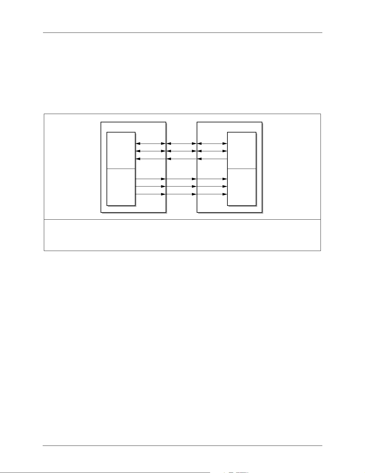
Functional Description CX23880/CX23881/CX23882/CX23883 Data Sheet
2.1.10.1 Normal Mode
Normal mode operation supports transfer of decoded broadcast audio samples to an
MPEG Encoder/CODEC or to nyquist-rate audio ADCs and DACs. No oversample
clock is provided and each I
LRCK, SDAT. This is illustrated in Figure 2-2. Normal mode is the default
configuration. It can also be programmed by writing 0x0 to the I
Figure 2-2. Normal Mode Operation
E4 Codec
2
S interface has its own dedicated three signals, SCK,
2
SCTL register.
GENERAL NOTE:
1. I2S In enabled.
2. I2S Out enabled.
3. No oversample clock provided.
I2S
In
I2S
Out
sck
Irclk
sdi
sck
Irclk
sdo
sck
Irclk
sd
sck
Irclk
sd
sck
Irclk
sdo
sck
Irclk
sdi
I2S
Out
I2S
In
101069_114
2-18 Conexant 101069A
Preliminary Information/Conexant Proprietary and Confidential 08/26/02
Page 49
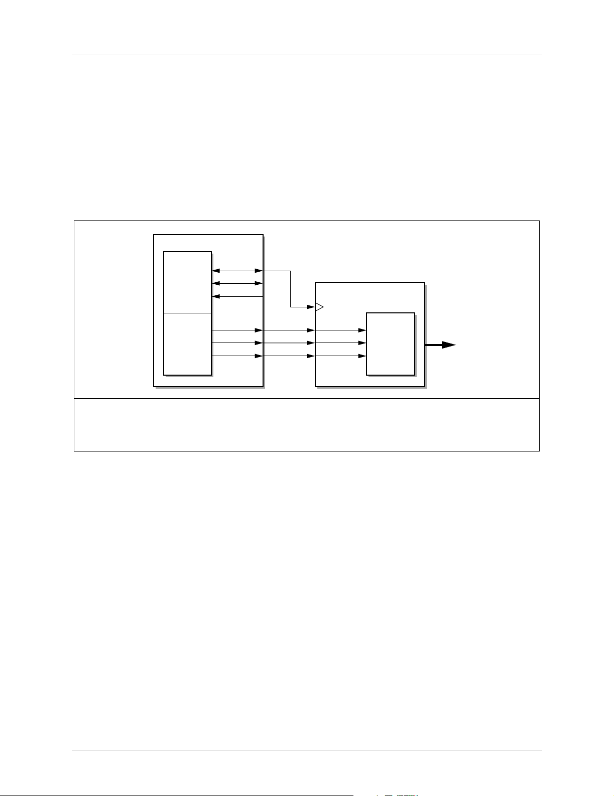
CX23880/CX23881/CX23882/CX23883 Data Sheet Functional Description
2.1.10.2 OSR DAC Mode
OSR DA C Mode is a va ilable to dri ve an e xternal high quality stereo audio D A C which
requires an oversampled clock. The I
input serial clock pin is used to output the oversampled clock. The I
still av ai lable.
OSR DAC mode is programmed by writing 0x2 to the I
2
SIN_ENABLE bit in the AUDCTL register must be disabled and the
the I
2
SOUT_ENABLE bit should be enabled. OSRDAC mode is illustrated in Figure 2-3.
I
Figure 2-3. OSR DAC Mode Operation
E4
I2S
In
I2S
Out
sck
Irclk
sdi
sck
Irclk
sdo
osck
sck
Irclk
sd
2
S input is not available in this mode. The I2S
2
SCTL register. Additionally,
OSR DAC
msck
sck
Irclk
sdi
I2S
In
2
S output pins are
Stereo
Audio Out
GENERAL NOTE:
1. I2S In disabled.
2. I2S Out enabled.
3. Oversample clock provided for DAC.
101069_115
101069A Conexant 2-19
08/26/02 Preliminary Information/Conexant Proprietary and Confidential
Page 50
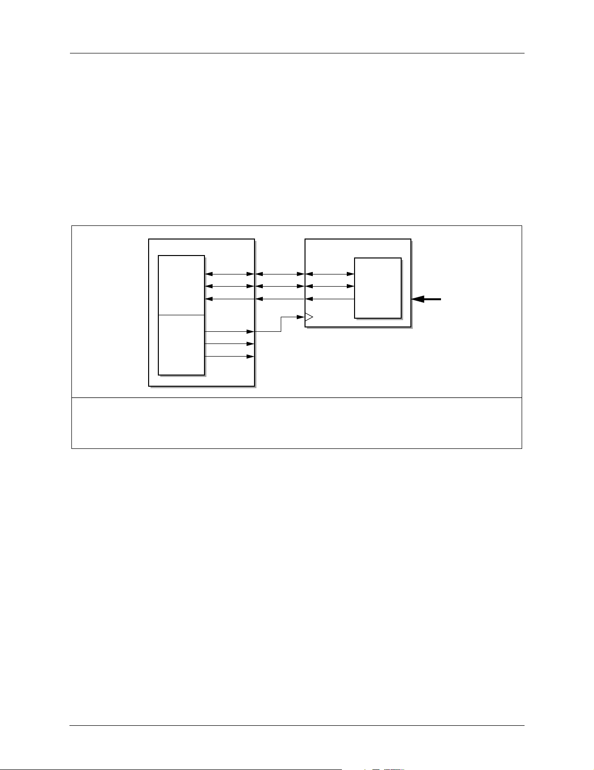
Functional Description CX23880/CX23881/CX23882/CX23883 Data Sheet
2.1.10.3 OSR ADC Mode
OSR ADC mode is available as an input for baseband stereo audio via an exter nal
audio ADC which requires an oversample clock. The I
mode. The I
input pins are still available for use.
OSR ADC mode is programmed by writing 0x1 to the I
2
SIN_ENABLE bit in the AUDCTL register should be enabled and the
the I
2
SOUT_ENABLE bit should be disabled. OSR ADC mode is illustrated in
I
Figure 2-4.
Figure 2-4. OSR ADC Mode Operation
E4
I2S
In
I2S
Out
2
2
S output serial clock pin is used to output the oversampled clock. The I2S
OSR ADC
sck
Irclk
sdi
sck
Irclk
sdo
sck
Irclk
sd
osck
sck
Irclk
sdo
msck
S output is not available in this
2
SCTL register. Additionally,
I2S
Out
Stereo
Audio In
GENERAL NOTE:
1. I2S In enabled.
2. I2S Out disabled.
3. Oversample clock provided for ADC.
101069_116
2-20 Conexant 101069A
Preliminary Information/Conexant Proprietary and Confidential 08/26/02
Page 51
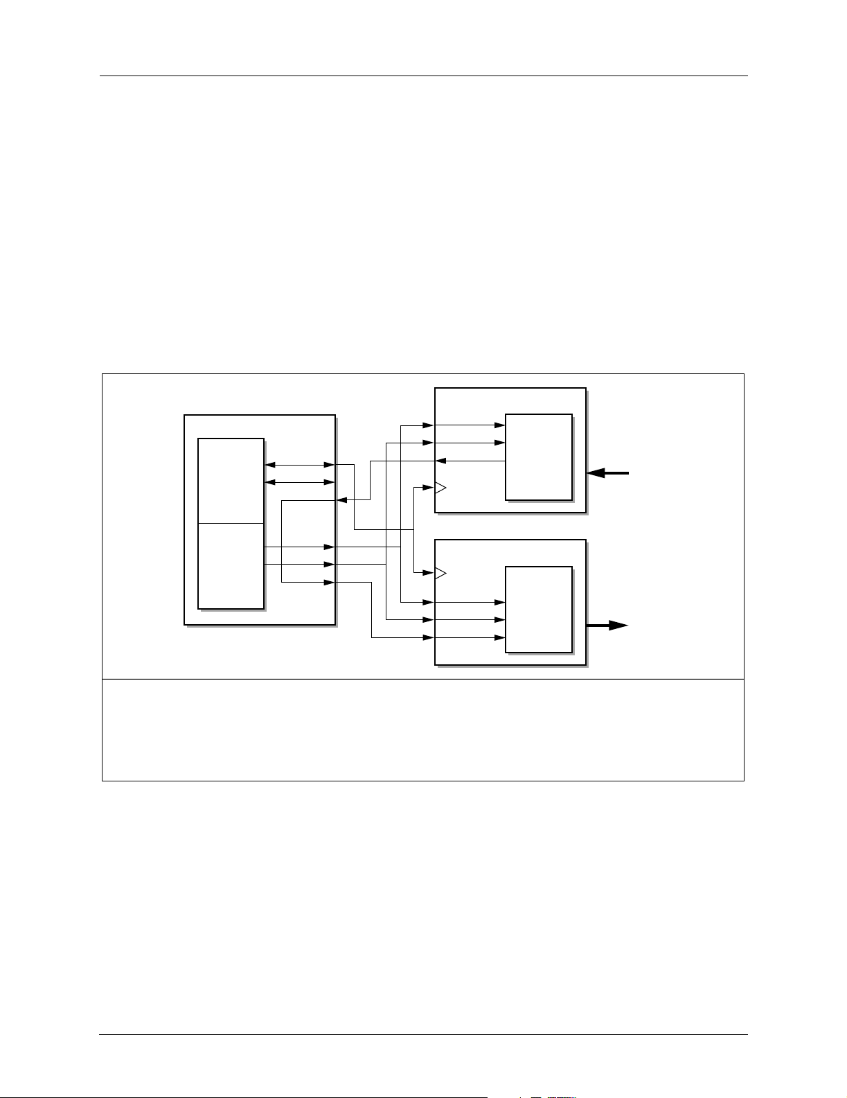
CX23880/CX23881/CX23882/CX23883 Data Sheet Functional Description
2.1.10.4 Pass-Thru Mode
Pass-Thru mode is provided as a method of making the CX2388 x act a s a mul tiplexer
between its o wn dig ital output from the broadca st audio decoder and the digit al output
from an I
clock. In this mode, the oversample clock is sent to the I
the external I
The I
data output pin. Both of the external I
This is illustrated in Figure 2-5.
Pass-thru mode is programmed by writing 0x8 to the I
the I
2
SOUT_ENABLE bit should be enabled.
I
Figure 2-5. Pass-Thru Mode Operation
E4
I2S
In
2
S input when either the I2S input or output (or both) require an oversample
2
2
S input serial data pin is internally connected directly to the I2S output serial
2
SIN_ENABLE bit in the AUDCTL register should be disabled and the
S devices are connected to the I2S output serial clock and word clock.
2
S devices must support slave-mode operation.
OSR ADC
sck
Irclk
sck
Irclk
sdi
sd
sdo
msck
2
S input serial clock pin. Both
2
SCTL register. Additionally,
I2S
Out
Stereo
Audio In
osck
sck
Irclk
sd
I2S
Out
sck
Irclk
sdo
GENERAL NOTE:
1. I2S In disabled.
2. I2S Out enabled.
3. External ADC and CODEC (or DAC) slaved to I2S Out.
4. I2S In serial data passed directly to I2S Out serial data.
5. Oversample clock provided for ADC and/or DAC.
Encoder or CODEC
msck
sck
Irclk
sdi
I2S
In
Compressed
Audio Out
101069_117
101069A Conexant 2-21
08/26/02 Preliminary Information/Conexant Proprietary and Confidential
Page 52

Functional Description CX23880/CX23881/CX23882/CX23883 Data Sheet
2.1.10.5 Full Functionality Mode
Full functionality mode is a vaila ble as a method for pro viding an o v ersampled clock to
external I
mode, the I
the external devices are both connected to the I
the ov ersample clock is provided on the I
data in to the I
separate. In this mode, it is possible to send broadcast data from the I
MPEG encoder or codec, while simultaneously streaming baseband stereo audio in
2
S input over the PCI, enabling DVCR record-one, play-another functionality
the I
with an S-Video or composite source with stereo inputs. Like the Pass-thru mode,
2
both I
Figure 2-6.
Full functionality mode is enabled b y programming 0x6 to the I
enables the oversample clock output on the I
2
S input off the I2S output serial clock and word clock internally. Additionally, the
I
2
SIN_ENABLE bit, and the I2SOUT_ENABLE bit in the AUDCTL register should
I
be enabled. Finally, the NS LAVEMASTER bit in the I
disabled to put the I
Figure 2-6. Full Functionality Mode
E4
I2S
In
2
S devices, while still maintaining separate I2S streams in and out. In this
2
S input is internally slaved to the I2S output serial clock and word clock,
2
S Input block and serial data out from the I2S Output block are kept
2
2
S output serial clock and word clock,
S output serial clock pin, and only the serial
2
S output to a
S devices must support slave mode operation. This mode is illustrated in
2
SCTL register, w hich
Stereo
Audio In
sdi
2
S Input into slave mode.
sck
Irclk
sd
sdo
msck
2
S input serial clock pin, and slaves the
2
SINPUT register should be
OSR ADC
I2S
Out
osck
sck
Irclk
sd
I2S
Out
sck
Irclk
sdo
GENERAL NOTE:
1. I2S In enabled.
2. I2S Out enabled.
3. External ADC and DAC slaved from I2S Out.
4. I2S In serial clock and word clock slaved from I2S Out.
5. Oversample clock provided for ADC and/or DAC.
msck
sck
Irclk
sdi
OSR DAC
I2S
In
Stereo
Audio Out
101069_118
2-22 Conexant 101069A
Preliminary Information/Conexant Proprietary and Confidential 08/26/02
Page 53
CX23880/CX23881/CX23882/CX23883 Data Sheet Functional Description
2.1.11 Audio DACs
The CX2388x provides an analog stereo audio output that can drive a PC audio card
or a stereo preamplifier input. Two integrated audio DACs provide approximately
85 dB SNR when used with an external active filter circuit, or approximately 75 dB
SNR when used with a simple RC external construction filter. See Chapter 3 for
external component example circuits.
NOTE:
Even when using the simple external RC filter, the audio system
performance exceeds the dynamic range inherent with broadcast audio
sources.
The input to the audio DACs is based on two bits present in the AUD_CTL register:
2
DA C_EN ABLE and I
S_STR2DA C. If D A C_EN ABLE is disabled, then no signals or
enables are passed to the D AC. If DAC_EN A BLE is enabled , the n either the I
2
S_STR2DAC is enabled) or the upstream DMA channel (if I2S_STR2DAC is
(if I
disabled) is passed to the DAC.
24'h32058C—AUD_CTL Register, Bits [12], [14]
Bits Type Default Name Description
[12] RW 1'b0 DAC_ENABLE DAC enable bit
[14] RW 1'b0 I
The DAC output sample rate is a fixed divide off the PLL clock. The sample rate is
calculated as the PLL frequency divided by 18 (the DAC pulse width modulated
output rate) and divided by 128 (the D AC oversampling ratio). Whiche v er sample rate
converter is used to dri ve the input to the D AC (through a FIFO) must be programmed
to this sample rate, not the 48 kHz s ample rate that is normally used. For instance, if
the demodulator is used as the source to the DAC, then the demodulator sample rate
converter DDS frequency must be programmed to provide output samples at the
calculated sample rate of the DAC instead of 48 kHz.
2
S_STR2DAC I2S input straight to DAC enable bit
2
S input
101069A Conexant 2-23
08/26/02 Preliminary Information/Conexant Proprietary and Confidential
Page 54

Functional Description CX23880/CX23881/CX23882/CX23883 Data Sheet
2.1.12 Broadcast Audio Programming Examples
Tables 2-11 through 2-15 list broadcast audio programming examples. Please contact
Conexant Applications Engineering to obtain updated programming examples.
Table 2-11. NICAM Broadcast Audio Decode and Output to Built-in Stereo DACs
Register Name Location Value Description
AFE_CFG_IO 24'h35C04C 32'h00000000 Enable audio DAC and video ADC bandgaps. Select audio mode.
AFE_12DB_EN 24'h320628 16'h0001 Enable +12 dB gain for audio signal from tuner
AUD_INIT 24'h320100 16'h0010 Configure NICAM broadcast audio
AUD_INIT_LD 24'h320104 16'h0001 Enable selected broadcast audio standard
AUD_SOF T_RESET 24'h320108 16'h0001 Enable audio soft reset. Keeps audio subsystem in a known state
until programming steps are complete.
AUD_RATE_ADJ1 24'h3205D8 16'h0010 Recommended values for NICAM setup
AUD_RATE_ADJ2 24'h3205DC 16'h0040 Recommended values for NICAM setup
AUD_RATE_ADJ3 24'h3205E0 16'h0100 Recommended values for NICAM setup
AUD_RATE_ADJ4 24'h3205E4 16'h0400 Recommended values for NICAM setup
AUD_RATE_ADJ5 24'h3205E8 16'h1000 Recommended values for NICAM setup
Location 32’h02320D01 32’h02320D01 8’h06 QAM setup
Location 32’h02320D02 32’h02320D02 8’h82 QAM setup
Location 32’h02320D03 32’h02320D03 8’h16 QAM setup
Location 32’h02320D04 32’h02320D04 8’h05 QAM setup
Location 32’h02320D2A 32’h02320D2A 8’h34 QAM setup
Location 32’h02320D2B 32’h02320D2B 8’h4C QAM setup
AUD_SOFT_RESET 24'h320108 16'h0000 Deassert audio soft reset
AUD_VOL_CTL 24'h32058C 16'h0000 Set volume control to 0 dB attenuation
2-24 Conexant 101069A
Preliminary Information/Conexant Proprietary and Confidential 08/26/02
Page 55
CX23880/CX23881/CX23882/CX23883 Data Sheet Functional Description
Table 2-12. FM Radio Decode and Output to Built-In Stereo DACs
Register Name Location Value Description
AFE_CFG_IO 24'h35C04C 32'h00000000 Enable audio DAC and video ADC bandgaps. Select audio
mode.
AFE_12DB_EN 24'h320628 16'h0001 Enable +12 dB gain for audio signal from tuner
AUD_INIT 24'h320100 16'h0020 Configure FM broadcast audio
AUD_INIT_LD 24'h320104 16'h0001 Enable selected broadcast audio standard
AUD_SOF T_RESET 24'h320108 16'h0001 Enable audio soft reset. Keeps audio subsystem in a known
state until programming steps are complete.
AUD_SOFT_RESET 24'h320108 16'h0000 Deassert audio soft reset
AUD_VOL_CTL 24'h32058C 6'h00 Set volume control to 0 dB attenuation
Table 2-13. BTSC Broadcast Audio Decode and Output to Built-in Stereo DACs
Register Name Location Value Description
AFE_CFG_IO 24'h35C04C 32'h00000000 Enable audio DAC and video ADC bandgaps. Select audio
mode.
AFE_12DB_EN 24'h320628 16'h0001 Enable +12 dB gain for audio signal from tuner
AUD_INIT 24'h320100 16'h0001 Configure BTSC broadcast audio
AUD_INIT_LD 24'h320104 16'h0001 Enable selected broadcast audio standard
AUD_SOF T_RESET 24'h320108 16'h0001 Enable audio soft reset. Keeps audio subsystem in a known
state until programming steps are complete.
AUD_DBX_IN_GAIN 24'h320500 16'hA5D0 Recommended values for BTSC setup
AUD_DBX_WBE_GAIN 24'h320504 16'h4163 Recommended values for BTSC setup
AUD_DBX_SE_GAIN 24'h320508 16'h5C0A Recommended values for BTSC setup
DEEMPH 0_G0 24’h320448 16’h0C02 Recommended values for BTSC setup
PHASE_FIX_CTL 24’h3205F0 16’h0030 Recommended values for BTSC setup
AUD_SOFT_RESET 24'h320108 16'h0000 Deassert audio soft reset
AUD_VOL_CTL 24'h32058C 6'h00 Set volume control to 0 dB attenuation
101069A Conexant 2-25
08/26/02 Preliminary Information/Conexant Proprietary and Confidential
Page 56

Functional Description CX23880/CX23881/CX23882/CX23883 Data Sheet
Table 2-14. EIAJ Broadcast Audio Decode and Output to Built-in Stereo DACs
Register Name Location Value Description
AFE_CFG_IO 24'h35C04C 32'h00000000 Enable audio DAC and video ADC bandgaps. Select audio
mode.
AFE_12DB_EN 24'h320628 16'h0001 Enable +12 dB gain for audio signal from tuner
AUD_INIT 24'h320100 16'h0002 Configure EIAJ broadcast audio
AUD_INIT_LD 24'h320104 16'h0001 Enable sele cted broadcast audio standard
AUD_SOFT_RESET 24'h320108 16'h0001 Enable audio soft reset. Keeps audio subsystem in a known
state until programming steps are complete.
AUD_RATE_ADJ1 24'h3205D8 16'h0100 Recommended values for EIAJ setup
AUD_RATE_ADJ2 24'h3205DC 16'h0200 Recommended values for EIAJ setup
AUD_RATE_ADJ3 24'h3205E0 16'h0300 Recommended values for EIAJ setup
AUD_RATE_ADJ4 24'h3205E4 16'h0400 Recommended values for EIAJ setup
AUD_RATE_ADJ5 24'h3205E8 16'h0500 Recommended values for EIAJ setup
AUD_THR_FR 24'h3203C0 16'h0000 Recommended values for EIAJ setup
AUD_PILOT_BQD_1_K0 24'h320380 32'h00008000 Recommended values for EIAJ setup
AUD_PILOT_BQD_1_K1 24'h320384 32'h00000000 Recommended values for EIAJ setup
AUD_PILOT_BQD_1_K2 24'h320388 32'h00000000 Recommended values for EIAJ setup
AUD_PILOT_BQD_1_K3 24'h32038C 32'h00000000 Recommended values for EIAJ setup
AUD_PILOT_BQD_1_K4 24'h320390 32'h00000000 Recommended values for EIAJ setup
AUD_PILOT_BQD_2_K0 24'h320394 32'h00C00000 Recommended values for EIAJ setup
AUD_PILOT_BQD_2_K1 24'h320398 32'h00000000 Recommended values for EIAJ setup
AUD_PILOT_BQD_2_K2 24'h32039C 32'h00000000 Recommended values for EIAJ setup
AUD_PILOT_BQD_2_K3 24'h3203A0 32'h00000000 Recommended values for EIAJ setup
AUD_PILOT_BQD_2_K4 24'h3203A4 32'h00000000 Recommended values for EIAJ setup
AUD_C2_UP_THR 24'h3203D8 16'h1000 Recommended values for EIAJ setup
AUD_C2_LO_THR 24'h3203DC 16'h0400 Recommended values for EIAJ setup
AUD_C1_UP_THR 24'h3203D0 16'h1800 Recommended values for EIAJ setup
AUD_C1_LO_THR 24'h3203D4 16'h1000 Recommended values for EIAJ setup
AUD_MODE_CHG_TIMER 24'h3205B4 16'h0080 Recommended values for EIAJ setup
AUD_START_TIMER 24'h3205B0 16'h0200 Recommended values for EIAJ setup
AUD_AFE_16DB_EN 24'h320628 16'h0001 Recommended values for EIAJ setup
AUD_DEEMPH0_G0 24'h320448 16'h23F8 Recommended values for EIAJ setup
AUD_PHASE_FIX_CTL 24'h3205F0 16'h0009 Recommended values for EIAJ setup
AUD_CORDIC_SHIFT_0 24'h320308 16'h0006 Recommended values for EIAJ setup
AUD_CORDIC_SHIFT_1 24'h320314 16'h0006 Recommended values for EIAJ setup
AUD_SOFT_RESET 24'h320108 16'h0000 Deassert audio soft reset
AUD_VOL_CTL 24'h32058C 16'h0000 Set volume control to 0 dB attenuation
2-26 Conexant 101069A
Preliminary Information/Conexant Proprietary and Confidential 08/26/02
Page 57

CX23880/CX23881/CX23882/CX23883 Data Sheet Functional Description
Table 2-15. A2 Broadcast Audio Decode and Output to Built-in Stereo DACs
Register Name Location Value Description
AFE_CFG_IO 24'h35C04C 32'h00000000 Enable audio DAC and video ADC bandgaps. Select audio
mode.
AFE_12DB_EN 24'h320628 16'h0001 Enable +12 dB gain for audio signal from tuner
AUD_INIT 24'h320100 16'h0004 Configure A2 broadcast audio
AUD_INIT_LD 24'h320104 16'h0001 Enable selected broadcast audio standard
AUD_SOF T_RESET 24'h320108 16'h0001 Enable audio soft reset. Keeps audio subsystem in a known
state until programming steps are complete
AUD_DMD_RA_DDS 24'h3205BC 32'h002A73BD Recommended values for A2 setup
AUD_RATE_ADJ1 24'h3205D8 16'h0100 Recommended values for A2 setup
AUD_RATE_ADJ2 24'h3205DC 16'h0200 Recommended values for A2 setup
AUD_RATE_ADJ3 24'h3205E0 16'h0300 Recommended values for A2 setup
AUD_RATE_ADJ4 24'h3205E4 16'h0400 Recommended values for A2 setup
AUD_RATE_ADJ5 24'h3205E8 16'h0500 Recommended values for A2 setup
AUD_THR_FR 24'h3203C0 16'h0000 Recommended values for A2 setup
AUD_PILOT_BQD_1_K0 24'h320380 32'h0001C000 Recommended values for A2 setup
AUD_PILOT_BQD_1_K1 24'h320384 32'h00000000 Recommended values for A2 setup
AUD_PILOT_BQD_1_K2 24'h320388 32'h00000000 Recommended values for A2 setup
AUD_PILOT_BQD_1_K3 24'h32038C 32'h00000000 Recommended values for A2 setup
AUD_PILOT_BQD_1_K4 24'h320390 32'h00000000 Recommended values for A2 setup
AUD_PILOT_BQD_2_K0 24'h320394 32'h00C00000 Recommended values for A2 setup
AUD_PILOT_BQD_2_K1 24'h320398 32'h00000000 Recommended values for A2 setup
AUD_PILOT_BQD_2_K2 24'h32039C 32'h00000000 Recommended values for A2 setup
AUD_PILOT_BQD_2_K3 24'h3203A0 32'h00000000 Recommended values for A2 setup
AUD_PILOT_BQD_2_K4 24'h3203A4 32'h00000000 Recommended values for A2 setup
AUD_C2_UP_THR 24'h3203D8 16'h1C00 Recommended values for A2 setup
AUD_C2_LO_THR 24'h3203DC 16'h1000 Recommended values for A2 setup
AUD_C1_UP_THR 24'h3203D0 16'h4C00 Recommended values for A2 setup
AUD_C1_LO_THR 24'h3203D4 16'h4000 Recommended values for A2 setup
AUD_MODE_CHG_TIMER 24'h3205B4 16'h0030 Recommended values for A2 setup
AUD_START_TIMER 24'h3205B0 16'h0200 Recommended values for A2 setup
AUD_AFE_16DB_EN 24'h320628 16'h0001 Recommended values for A2 setup
AUD_CORDIC_SHIFT_0 24'h320308 16'h0006 Recommended values for A2 setup
AUD_SOFT_RESET 24'h320108 16'h0000 Deassert audio soft reset
AUD_VOL_CTL 24'h32058C 16'h0000 Set volume control to 0 dB attenuation
101069A Conexant 2-27
08/26/02 Preliminary Information/Conexant Proprietary and Confidential
Page 58
Functional Description CX23880/CX23881/CX23882/CX23883 Data Sheet
2.2 General Purpose Host Port
2.2.1 Introduction
The CX23880/CX23882 features a general purp ose bidirectional host processor
interface. This enables board vendors to add additional components to a basic
CX2388x design to create value-added products based around a broadcast capture
solution that capitalizes on the explosion of interest in digital video and broadband
data.
Table 2-16 gives some examples of peripherals that can be added to the CX23880/
CX23882's host port to create higher functionality and differentiated products.
Table 2-16. CX23880/CX23882 Applications Enabled by Host Port Peripherals
Application
Digital VCR Conexant MPEG Encoder IC
Cable Modem PC/TV Conexant Cable Modem IC
PC/TV with IR remote control IR Controller
Video Editor DV Codec
2.2.2 Host Port Overview
The General Purpose Host Port (GPHP) supports peripherals that conform to either
Motorola- or Intel-style bus interface signaling protocols, with appropriate big endian
vs. little endian byte ordering. The GPHP supports either discrete or multiplexed
address/data buses as follows:
! 8-bit data path and 8-bit address on a nonmultiplexed bus
! 16-bit data path and 16-bit address on a multiplexed bus
The GPHP allows simultaneous connection to two peripheral ICs with no external
interface logic, or four peripheral ICs with external glue logic. The function of the
glue logic is to decode the chip select information encoded onto the two chip select
pins when in encoded chip select mode. The GPHP can then be used t o gain access to
the memory map of these external devices for register reads and writes.
The GPHP interface is configurable via the host interface registers. These registers
allow for the se lec tio n o f the bus size, handshaking mode, signal polarity, and control
signal timing adjustment.
ICs that connect to the
CX23880/CX23882 General Purpose Host Port
2-28 Conexant 101069A
Preliminary Information/Conexant Proprietary and Confidential 08/26/02
Page 59
CX23880/CX23881/CX23882/CX23883 Data Sheet Functional Description
The GPHP pin interface is defined in Table 2-17.
Table 2-17. GPHP Pin Definition
Pin Number Pin Name Dir Full Name Description: GPHP Signals
91, 92, 93, 94, 95,
96, 97, 98, 99,
100, 101, 106,
HAD[15:0] I/O General Purpose Host
Address/Data
Bidirectional address/data access bus. The width is
selectable between an 8-bit address and 8-bit data
bus or a multiplexed 16-bit address/data bus.
107, 108, 109,
110
90 HCS# O General Purpose Host Chip
External Chip select
Select
89 HRD/HDS# O General Purpose Host Read/
Data Strobe
Either the active low read signal (Intel mode) or the
programmable polarity data strobe signal (Motorola
mode).
87 HWR/HRW# O General Purpose Host Write/
Read NOT Write
88 HALE# O General Purpose Host
Address Latch Enable
Either the active low write signal (Intel mode) or the
read/not write (Motorola mode).
Address Latch Enable signal. Used only in multiplexed
16-bit address/data mode.
86 HRDY# I General Purpose Host Ready External data transfer acknowledge signal
85 HEXFB I General Purpose Host
External Status
Handshaking signal for use in DMA mode to indicate
the status of the external source or destination FIFO.
101069A Conexant 2-29
08/26/02 Preliminary Information/Conexant Proprietary and Confidential
Page 60
Functional Description CX23880/CX23881/CX23882/CX23883 Data Sheet
Host Wait-State Control
24'h380054—HST_WSC Register
Bits Type Default Name Description
[31:28] RW 4’h1 HST_W3W Wait state control for external write cycles to chip select:
HCS[3]#. Length of write cycle = (register value * bclk
period)
[27:24] RW 4’h1 HST_W2W HCS[2] write cycle.
[23:20] RW 4’h1 HST_W1W HCS[1] write cycle.
[19:16] RW 4’h1 HST_W0W HCS[0] write cycle.
[15:12] RW 4’h1 HST_W3R Wait state control for external read cycles to chip select:
HCS[3]#. Length of write cycle = (register value * bclk
period)
[11:8] RW 4’h1 HST_W2R HCS[2] read cycle.
[7:4] RW 4’h1 HST_W1R HCS[1] read cycle.
[3:0] RW 4’h1 HST_W0R HCS[0] read cycle.
Host Transfer Control
24'h380058—HST_XFER_CNTL Register
Bits Type Default Name Description
[15] RW 1’b0 Hcs3_cs_hold HCS[3] chip select hold time (15ns) relative to read or write
enable (1 = On, 0 = Off)
[14] RW 1’b0 Hcs2_cs_hold HCS[2] chip select hold time
[13] RW 1’b0 Hcs1_cs_hold HCS[1] chip select hold time
[12] RW 1’b0 Hcs0_cs_hold HCS[0] chip select hold time
[11] RW 1’b0 Hcs3_ds_polarity External Data Strobe polarity for HCS[3](1 = positive,
0 = negative) Motorola mode only.
[10] RW 1’b0 Hcs2_ds_polarity External Data Strobe polarity for HCS[2]
[9] RW 1’b0 Hcs1_ds_polarity External Data Strobe polarity for HCS[1]
[8] RW 1’b0 Hcs0_ds_polarity External Data Strobe polarity for HCS[0]
[7] RW 1’b0 Hcs3_xfer_mode External Transfer mode for HCS[3](we# & re# or r/w# &
ds#) (intel(0) or Motorola(1)
[6] RW 1’b0 Hcs2_xfer_mode External Transfer mode for HCS[2]
[5] RW 1’b0 Hcs1_xfer_mode External Transfer mode for HCS[1]
[4] RW 1’b0 Hcs0_xfer_mode External Transfer mode for HCS[0]
[3] RW 1’b0 Hcs2_sh_extend External data setup and hold time extend for HCS[3]
(0 = 1x bclk period 1 = 2x bclk period)
[2] RW 1’b0 Hcs2_sh_extend External setup and hold extend for HCS[2]
[1] RW 1’b0 Hcs1_sh_extend External setup and hold extend for HCS[1]
[0] RW 1’b0 Hcs0_sh_extend External setup and hold extend for HCS[0]
2-30 Conexant 101069A
Preliminary Information/Conexant Proprietary and Confidential 08/26/02
Page 61

CX23880/CX23881/CX23882/CX23883 Data Sheet Functional Description
Host Interface Width
24'h38005C—EXT_INTF_WIDTH Register
Bits Type Default Name Description
[3] RW 1’b0 Ext_intf_width[3] HCS3 : (0) : 16-bit (multiplexed), (1): 8-bit
[2] RW 1’b0 Ext_intf_width[2] HCS2 : (0) : 16-bit (multiplexed), (1): 8-bit
[1] RW 1’b0 Ext_intf_width[1] HCS1 : (0) : 16-bit (multiplexed), (1): 8-bit
[0] RW 1’b0 Ext_intf_width[0] HCS0 : (0) : 16-bit (multiplexed), (1): 8-bit
Host Peripheral Handshake
24'h380060—HRDY_HANDSHAKE Register
Bits Type Default Name Description
[3] RW 1’b0 Mstr_handshake[3] HCS3 HRDY handshake enable bit
[2] RW 1’b0 Mstr_handshake[2] HCS2 HRDY handshake enable bit
[1] RW 1’b0 Mstr_handshake[1] HCS1 HRDY handshake enable bit
[0] RW 1’b0 Mstr_handshake[0] HCS0 HRDY handshake enable bit
Host Multiplexed 16-bit Transfer Parameters
24'h380064—MUX16_PARAM Register
Bits Type Default Name Description
[31:28] RW 4’b0001 HCS3_ale_timing HCS3 HRDY handshake enable bit
[27:24] RW 4’b0001 HCS2_ale_timing HCS2 HRDY handshake enable bit
[23:20] RW 4’b0001 HCS1_ale_timing HCS1 HRDY handshake enable bit
[19:16] RW 4’b0001 HCS0_ale_timing HCS0 HRDY handshake enable bit
[15:12] RW 4’b0010 HCS3_addr_cyc HCS3 Address cycle width (register value * bclk period)
setup time not included
[11:8] RW 4’b0010 HCS2_addr_cyc HCS2 Address cycle width
[7:4] RW 4’b0010 HCS1_addr_cyc HCS1 Address cycle width
[3:0] RW 4’b0010 HCS0_addr_cyc HCS0 Address cycle width
101069A Conexant 2-31
08/26/02 Preliminary Information/Conexant Proprietary and Confidential
Page 62
Functional Description CX23880/CX23881/CX23882/CX23883 Data Sheet
Host Chip Select Mode
24'h380068—HCS_MODE_SEL Register
Bits Type Default Name Description
[0] RW 1’b0 HCS_mode_sel This bit selects between the two possible chip select
modes:
0 : 2-bit dedicated chip selects. For times when two or
fewer devices are connected to the host port.
1 : 2-bit encoded chip selects. For times when more than
two devices are connected to the host port.
Host Software Reset
24'h38C06C—HOST_SOFT_RST Register
Bits Type Default Name Description
[0] WO 1’b0 HOST_SOF T_RST Host Software Reset. Writing a one to this register triggers
a reset of the host logic.
Host Interrupt Mask
24'h200090—HST_INT_MSK Register
Bits Type Default Name Description
[19:0] RW 20’b0 HST_INT_MASK A value of 1 enables the corresponding interrupt bit
location in the HST_INT_STAT register. Unmasking a bit
may generate an interrupt immediately due to a previously
pending condition. The interrupt remains asserted until the
device driver clears or masks the pending request.
2-32 Conexant 101069A
Preliminary Information/Conexant Proprietary and Confidential 08/26/02
Page 63

CX23880/CX23881/CX23882/CX23883 Data Sheet Functional Description
Host Interrupt Status
24'h200094—HST_INT_STAT Register
Bits Type Default Name Description
[19] RR 1’b0 PCI_ABORT Se t when the PCI master does a master-abort, or a target
responds with a target-abort.
[18] RR 1’b0 RIP_ERR Set when a data parity error is detected (parity error
response must be set while the master is reading RISC
instructions.
[17] RR 1’b0 PAR_ERR Set when a parity error is detected on the PCI bus for any
of the transactions, R/W, address/data phases, master/
target, regardless of the parity error response bit.
[16] RR 1’b0 OPC_ERR Set when the RISC controller detects a reserved/unused
opcode in the instruction sequence.
[13] RR 1’b0 UP_SYNC Set when number of lines or bytes do not match the
upstream host RISC program expectations.
[12] RR 1’b0 DN_SYNC Set when number of lines or bytes do not match the
downstream host RISC program expectations.
[9] RR 1’b0 UPF_UF Set when upstream host FIFO underflow condition is being
handled.
[8] RR 1’b0 DNF_OF Set when downstream host FIFO overflow condition is
being handled.
[5] RR 1’b0 UP_RISCI2 Set when the IRQ2 bit in a upstream host RISC instruction
is set.
[4] RR 1’b0 DN_RISCI2 Set when the IRQ2 bit in a downstream host RISC
instruction is set.
[1] RR 1’b0 UP_RISCI1 Set when the IRQ1 bit in a upstream host RISC instruction
is set.
[0] RR 1’b0 DN_RISCI1 Set when the IRQ1 bit in a downstream host RISC
instruction is set.
101069A Conexant 2-33
08/26/02 Preliminary Information/Conexant Proprietary and Confidential
Page 64
Functional Description CX23880/CX23881/CX23882/CX23883 Data Sheet
Host Interrupt Masked Status
24'h200098—HST_INT_MSTAT Register
Bits Type Default Name Description
[19:0] RO 20’b0 HST_INT_MSTAT These bits are the logical AND of the corresponding bits in
the status and mask registers.
Host Interrupt Set Status
24'h20009C—HST_INT_SSTAT Register
Bits Type Default Name Description
[16:0] WO 17’b0 HST_INT_SSTAT Writing a 1 to these bits will set the corresponding bits in
the status register.
The GPHP can support one upstream DMA (transfer from host to peripheral via
CX23880/CX23882) and one downstream (transfer from peripheral to host via the
CX23880/CX23882) DMA channel active at any time. These DMA channels are
configured by the EPHP DMA registers and are detailed in Table 2-17.
2-34 Conexant 101069A
Preliminary Information/Conexant Proprietary and Confidential 08/26/02
Page 65
CX23880/CX23881/CX23882/CX23883 Data Sheet Functional Description
IPB DMAC Current Buffer Pointer
24'h3000A8—DMA31_PTR1 Register
24'h3000AC—DMA32_PTR1 Register
Bits Type Default Name Description
[23:2] RO 22’hxxxxxx DMA{x}_PTR1 Current DMA qword address pointer. Points to next qword
transfer location within source or destination buffer . Always
dword-aligned.
[1:0] RO 2’b00 Reserved
IPB DMAC Current Table Pointer
24'h3000E8—DMA31_PTR2 Register
24'h3000EC—DMA32_PTR2 Register
Bits Type Default Name Description
[23:2] RW* 22’hxxxxxx DMA{x}_PTR2 Current DMA CDT address pointer. Points to current CDT
entry. Always dword-aligned.
[1:0] RO 2’b00 Reserved
IPB DMAC Buffer Limit
24'h300128—DMA31_CNT1 Register
24'h30012C—DMA32_CNT1 Register
Bits Type Default Name Description
[10:0] RW* 11’hxxx DMA{x}_CNT1 Initialize to DMA buffer size in # of qwords. Increments
during DMA data transfers and reloads when next CDT
pointer is fetched.
IPB DMAC Table Size
24'h300168—DMA31_CNT2 Register
101069A Conexant 2-35
08/26/02 Preliminary Information/Conexant Proprietary and Confidential
Page 66
Functional Description CX23880/CX23881/CX23882/CX23883 Data Sheet
24'h30016C—DMA32_CNT2 Register
Bits Type Default Name Description
[10:0] RW* 11’hxxx DMA{x}_CNT2 Initialize to DMA CDT size in # of qwords.
General Purpose Counter (Immediate access)
24'h38C020—HSTD_GP_CNT Register
24'h38C024—HSTU_GP_CNT Register
Bits Type Default Name Description
[15:0] RO 16’b0 {x}_GP_CNT General purpose counter used by RISC program.
General Purpose Counter Control (Immediate access)
24'h38C030—HSTD_GP_CNT_CNTRL Register
24'h38C034—HSTU_GP_CNT_CNTRL Register
Bits Type Default Name Description
[1:0] WO 2’b00 {x}_GP_CNT_CNTRL General purpose counter control used by RISC program:
00 = no change
01 = increment
10 = reserved
11 = reset to 0
Host Interface Streaming Enable (Immediate access)
24'h38C040—HST_STREAM_EN Register
Bits Type Default Name Description
[5] RW 1’b0 HSTU_RISC_EN RISC Controller enable for the host interface upstream
DMA channel.
[4] RW 1’b0 HSTD_RISC_EN RISC Controller enable for the host interface downstream
DMA channel
[1] RW 1’b0 HSTU_FIFO_EN Enable for pulling data out of the host upstream DMA FIFO
or cluster descriptor table.
[0] RW 1’b0 HSTD_FIFO_EN Enable for fetching downstream data from the external
source.
2-36 Conexant 101069A
Preliminary Information/Conexant Proprietary and Confidential 08/26/02
Page 67

CX23880/CX23881/CX23882/CX23883 Data Sheet Functional Description
Host Upstream DMA Control Register #1
24'h380048—HSTU_DMA_CTRL1 Register
Bits Type Default Name Description
[25] RW 1’b0 UP_FIFO_HK_EN Host upstream FIFO handshake enable. This enables the
CX23880/CX23882 to monitor the External_fifo_busy bit
and act accordingly.
[24] RW 1’b0 HSTU_AINC_EN Host upstream address auto-increment enable. Used to
DMA data to sequential addresses within the slave device.
Not to be used when the destination is a FIFO.
[23:0] RW 24’hxxxxxx HSTU_DST_ADDR HST upstream IPB DMA Destination address. If auto-
increment is enabled then the value loaded into this register
should be the starting address.
Host Downstream DMA Control Register #1
24'h38004C—HSTD_DMA_CTRL1 Register
Bits Type Default Name Description
[25] RW 1’b0 DN_FIFO_HK_EN Host downstream FIFO handshake enable. This enables
CX23880/CX23882 to monitor the External_fifo_busy bit
and act accordingly.
[24] RW 1’b0 HSTD_AINC_EN Host downstream address auto-increment enable. Used to
DMA data to sequential addresses within the slave device.
Not to be used when the destination is a FIFO.
[23:0] RW 24’hxxxxxx HSTD_SRC_ADDR HOST downstream IPB DMA source address. If auto
increment is enabled then the value loaded into this register
should be the starting address.
Host Downstream DMA Control Register #2
24'h380050—HSTD_DMA_CTRL2 Register
Bits Type Default Name Description
[11:0] RW 12’b0 HST_LNGTH HST downstream transfer count in bytes.
101069A Conexant 2-37
08/26/02 Preliminary Information/Conexant Proprietary and Confidential
Page 68
Functional Description CX23880/CX23881/CX23882/CX23883 Data Sheet
2.2.3 General Purpose Host Port Memory Space
The memory space associated with the GPHP is divided into two categories, internal
registers and the external peripheral address space. Table 2-18 provides descriptions
of each address range in the GPHP memory space.
Table 2-18. GPHP Memory Space
ADDRESS RANGE SIZE DESCRIPTION
380000–38FFFF 64 KB HOST local registers, specific to the CX23880
390000–39FFFF 64 KB Peripheral 1 address space
3A0000–3AFFFF 64 KB Peripheral 2 address space
3B0000–3BFFFF 64 KB Peripheral 3 address space
3C0000–3CFFFF 64 KB Peripheral 4 address space
2.2.4 General Purpose Host Port Interface Register Access
There are 64 KB of address space available within the GPHP address space for each
of the four possible peripherals and all of the registers pertaining to the GPHP
configuration. For the peripherals that are connected to the CX23880/CX223882 via
the 8-bit data interface, only the lower 256 bytes of this space are accessible. This
register mapping allows the peripherals to ha v e their registers directl y mapped into the
CX23880/CX23882 memory map.
2.2.5 General Purpose Host Interface External DMA Transfers
Streaming of data upstream and downstream is achieved via the DMA mechanis m
resident in the GPHP. There are two dedicated DMA channels that are available One
channel is dedicated to upstream DMA while the other is dedicated to downstream
DMA.
Once the DMAC is set up for the transfer, the GPHP must be configured. This
configuration consists of the programming of the GPHP DMA Setup registers. F or
upstream transfers, the GPHP must be programmed with the external destination
address, auto increment enable/disable, and end-of-transfer interrupt enable. For
downstream transfers, the GPHP must be programmed with the external source
address, byte count, auto increment enable/disable, and end-of-transfer interrupt
enable. These reads and writes are then forwarded by the GPHP to the appropriate
external source or destination address.
Upon completion of a packet of data, the GPHP generates the appropriate DMA
interrupt.
The GPHP uses its external FIFO status pin to interface with an external streaming
FIFO. When enabled, this pin is used to indicate when the external destination can
safely accept more data in the upstream case, and when the external source has data to
transfer in the downstream case. Because there are two DMA channels and only one
FIFO status pin, one of the two DMA chan nels must use the re gi ster polling app roach
to obtain the FIFO status in the case where both channels are being used
simultaneously.
2-38 Conexant 101069A
Preliminary Information/Conexant Proprietary and Confidential 08/26/02
Page 69
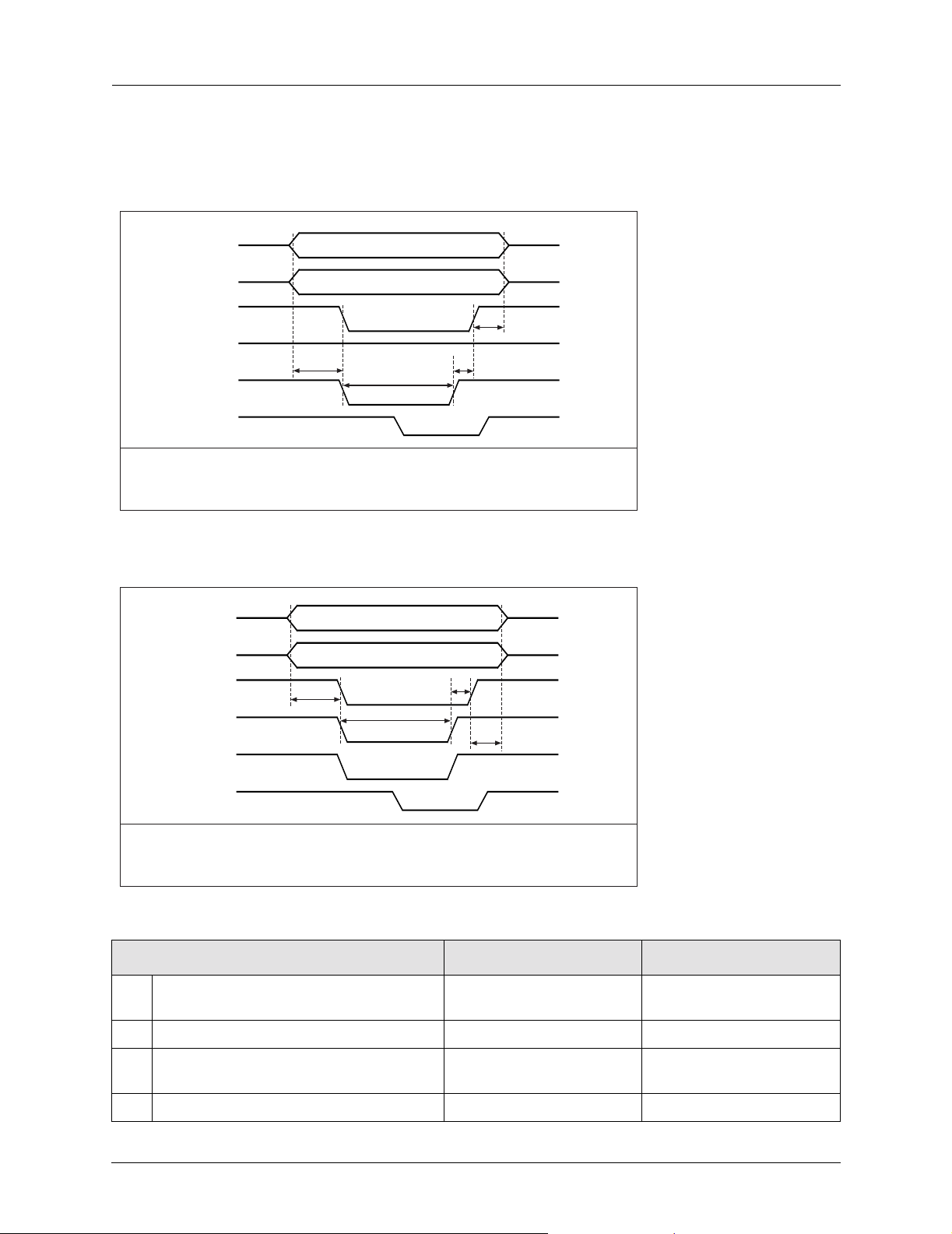
CX23880/CX23881/CX23882/CX23883 Data Sheet Functional Description
2.2.6 General Purpose Host Interface Signaling—Nonmultiplexed Mode
Figure 2-7. Host Interface Write Operation—Intel Style (Accessing an External Device)
HAD[15:8]
HAD[7:0]
HCS[X]#
HRD#
1
HWR#
1
HRDY#
A
Address
Data
D
C
B
NOTE(S):
! The HRDY# signal only used for handshaking when it is enabled via one of the host registers.
! HRDY# has programmable polarity. HRDY# is shown here in its default setting, active low.
101069_059
Figure 2-8. Host Interface Write Operation—Motorola Style (Accessing an External Device)
HAD[15:8]
HAD[7:0]
HCS[X]#
HR/W#
2
A
Address
Data
C
B
D
HDS#
2
HRDY#
NOTE(S):
! The HRDY# signal only used for handshaking when it is enabled via one of the host registers.
! HRDY# and HDS# each have programmable polarity. Both are shown here in their default settings, active low.
101069_060
Description Min Max
A Addr/Data setup time relative to write pulse and
1x PCLK Period 2x PCLK Period
chip select and HDS pulse
B Write pulse width, HDS pulse width 1x PCLK Period 15x PCLK Period
C Chip select hold time relative to write pulse and
0 1x PCLK Period
HDS pulse
D Addr/Data hold time relative to chip select 1x PCLK Period 2x PCLK Period
101069A Conexant 2-39
08/26/02 Preliminary Information/Conexant Proprietary and Confidential
Page 70
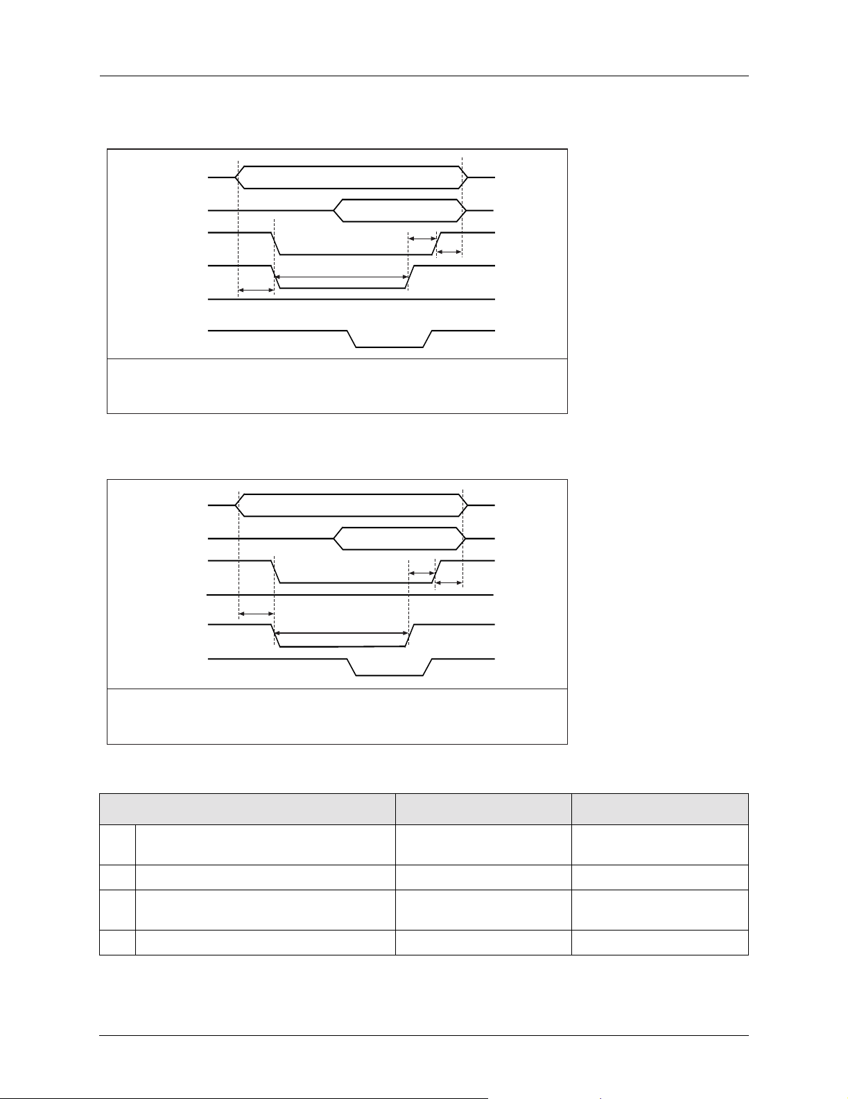
Functional Description CX23880/CX23881/CX23882/CX23883 Data Sheet
Figure 2-9. Host Interface Read Operation—Intel Style (Accessing an External Device)
HAD[15:8]
HAD[7:0]
HCS[X]#
HR/W#
A
HDS#
HRDY#
Address
Data
C
D
B
NOTE(S):
! The HRDY# signal only used for handshaking when it is enabled via one of the host registers.
! HRDY# has programmable polarity. HRDY# is shown here in its default setting, active low.
101069_061
Figure 2-10. Host Interface Read Operation—Motorola Style (Accessing an External Device)
HAD[15:8]
HAD[7:0]
HCS[X]#
HR/W#
A
HDS#
Address
B
Data
C
D
HRDY#
NOTE(S):
! The HRDY# signal only used for handshaking when it is enabled via one of the host registers.
! HRDY# and HDS# each have programmable polarity. Both are shown here in their default settings, active low.
101069_062
Description Min Max
A Addr/Data setup time relative to write pulse and
1x PCLK Period 2x PCLK Period
chip select and HDS pulse
B Write pulse width, HDS pulse width 1x PCLK Period 15x PCLK Period
C Chip select hold time relative to write pulse and
0 1x PCLK Period
HDS pulse
D Addr hold time relative to chip select 1x PCLK Period 2x PCLK Period
2-40 Conexant 101069A
Preliminary Information/Conexant Proprietary and Confidential 08/26/02
Page 71

CX23880/CX23881/CX23882/CX23883 Data Sheet Functional Description
2.2.7 General Purpose Host Interface Signaling—Multiplexed Mode
Figure 2-11. Host Interface Read Operation—Intel Style Multiplexed Address/Data Bus (Accessing an External Device)
HAD[15:0]
HALE
HCS[X]#
HRD#
HWR#
HRDY#
Address Data
C
B
E
A
D
NOTE(S):
! The HRDY# signal only used for handshaking when it is enabled via one of the host registers.
! HRDY# has programmable polarity. HRDY# is shown here in its default setting, active low.
101069_063
Figure 2-12. Host Interface Read Operation—Motorola Style Multiplexed Address/Data Bus (Accessing an External
Device)
HAD[15:0]
HALE
HCS[X]#
HR/W#
Address Data
C
B
E
A
D
HDS#
HRDY#
NOTE(S):
! The HRDY# signal only used for handshaking when it is enabled via one of the host registers.
! HRDY# and HDS# each have programmable polarity. Both are shown here in their default settings, active low.
101069_064
101069A Conexant 2-41
08/26/02 Preliminary Information/Conexant Proprietary and Confidential
Page 72
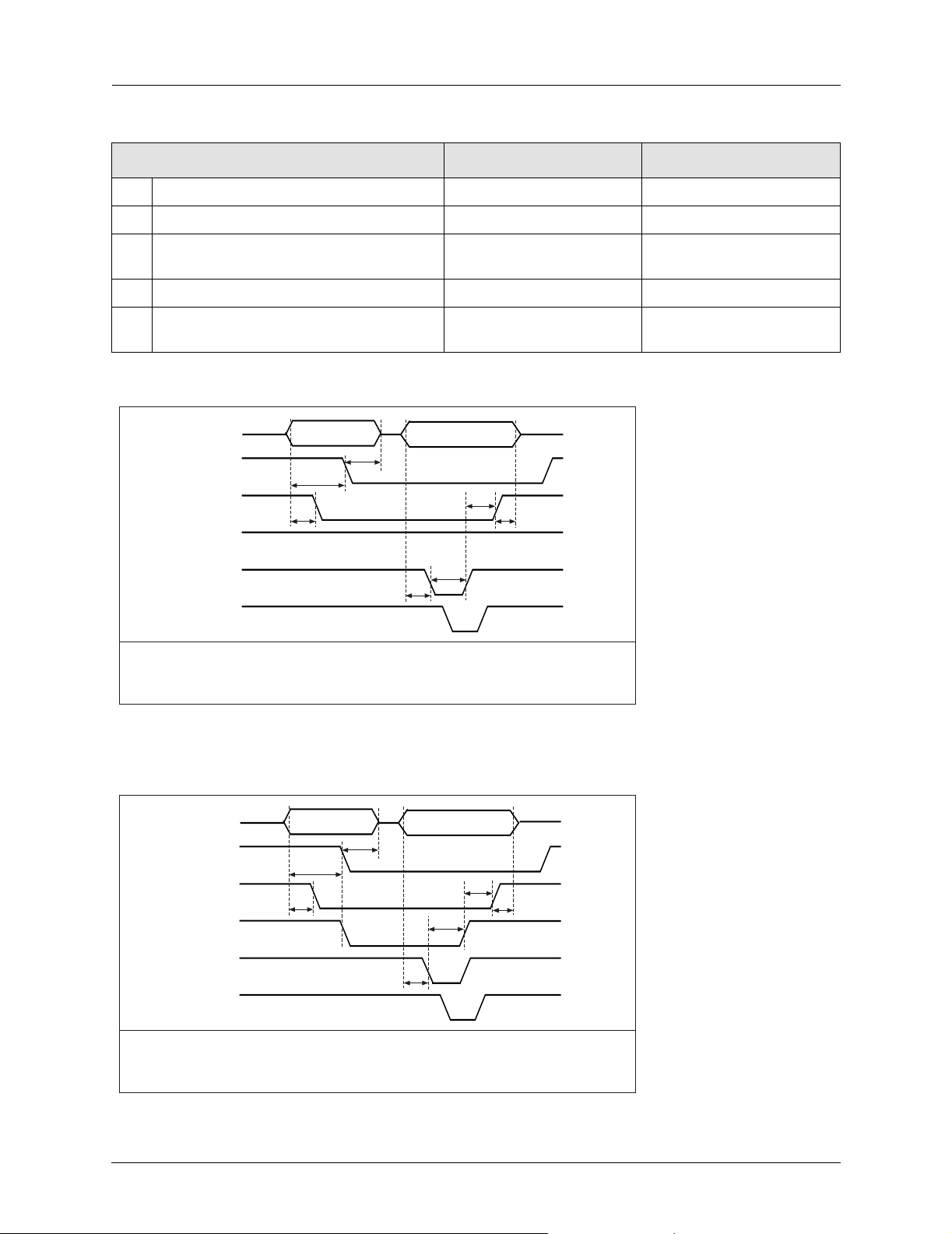
Functional Description CX23880/CX23881/CX23882/CX23883 Data Sheet
Description Min Max
A Addr/Data setup time to chip select 1x PCLK Period 2x PCLK Period
B Addr setup time relative to HALE 2x PCLK Period 3x PCLK Period
C Chip select hold time relative to address latch
1x PCLK Period 1x PCLK Period
enable
D Read pulse width, HDS pulse width 1x PCLK Period 15x PCLK Period
E Chip select hold time relative to read pulse and
0 1x PCLK Period
HDS pulse
Figure 2-13. Host Interface Write Operation—Intel Style Multiplexed Address/Data Bus (Accessing an External Device)
HAD[15:0]
HALE
HCS[X]#
HRD#
HWR#
HRDY#
Address Data
C
B
A
D
F
G
E
NOTE(S):
! The HRDY# signal only used for handshaking when it is enabled via one of the host registers.
! HRDY# has programmable polarity. HRDY# is shown here in its default setting, active low.
101069_065
Figure 2-14. Host Interface Write Operation—Motorola Style Multiplexed Address/Data Bus (Accessing an External
Device)
HAD[15:0]
HALE
HCS[X]#
HR/W#
HDS#
HRDY#
Address Data
C
B
A
D
F
G
E
NOTE(S):
! The HRDY# signal only used for handshaking when it is enabled via one of the host registers.
! HRDY# and HDS# each have programmable polarity. Both are shown here in their default settings, active low.
101069_066
2-42 Conexant 101069A
Preliminary Information/Conexant Proprietary and Confidential 08/26/02
Page 73
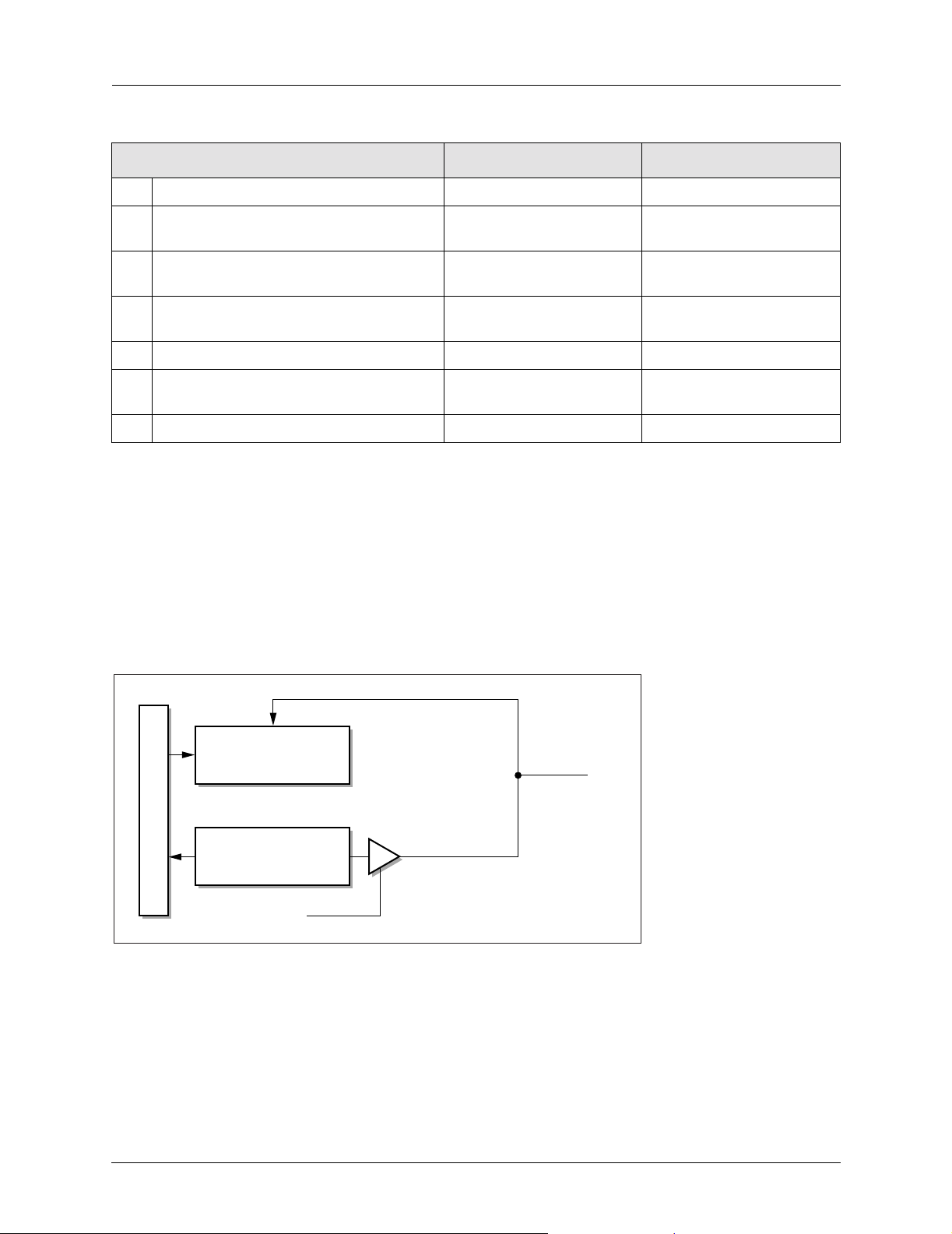
CX23880/CX23881/CX23882/CX23883 Data Sheet Functional Description
Description Min Max
A Addr setup time relative to chip select 1x PCLK Period 2x PCLK Period
B Addr setup time relative to address latch enable
2x PCLK Period 3x PCLK Period
(hale) and HR/W#
C Addr hold time relative to address latch enable
1x PCLK Period 1x PCLK Period
(hale)
D Data setup relative to (Intel) write pulse or (Moto)
1x PCLK Period 1x PCLK Period
HDS pulse
E (Intel) Write pulse width (Moto) HDS pulse width 1x PCLK Period 15x PCLK Period
F Chip select hold time relative to write pulse and
0 1x PCLK Period
HDS pulse
G Data hold time relative to the chip select 1x PCLK Period 2x PCLK Period
2.3 General Purpose Input/Output
2.3.1 GPIO Pin Architecture
Each General Purpose Input/Output (GPIO) pin is set up as a basic I/O buffer, with
each bit of the General Purpose Output Enable (GPOE) register used to enable an
individual pin’s output driver (see Figure 2-15).
Figure 2-15. GPIO Pin Architecture
L
o
c
a
l
R
e
g
i
s
t
e
r
GPDATA Input/
Read Buffer/Register
GPDATA Output/
Write Holding Register
GP_OE[x]
GPIO[x]
Three-State
Buffer
101069_023
101069A Conexant 2-43
08/26/02 Preliminary Information/Conexant Proprietary and Confidential
Page 74

Functional Description CX23880/CX23881/CX23882/CX23883 Data Sheet
2.3.2 GPIO Modes in CX2388x
Twenty-four pins are provided for GPIO . They are mapped onto the pin numbers liste d
in Table 2-19.
Table 2-19. GPIO Pin Numbers
Pin Numbers GPIO Number
8–15 [23–16]
112–119 [15–8]
123–130 [7–0]
The GPIO port is highly flexible and can be assigned to the following functions with
the CX23880. F o r CX23 88 1/CX23883, not all of these functions are available. See
Table 1-1.
! General purpose I/O functions
! MPEG input parallel port (DVB common interface-compatible)
! VIP parallel host port expansion
! Digital video output from the vi deo decoder as either 8-bit or 10-bi t, 4:2:2 samples
with 601-like external synchronization signals
! Digital video output from the video decoder as 8-bit, ITU-R656, 27 MHz, 4:2:2
samples
! Digital video input to the CX238880/CX23882 image scaler (and subsequent
DMA to VGA overlay surface) from an external MPEG decoder outputting ITUR656, 27 MHz, 4:2:2 interlaced samples or 54 MHz noninterlaced video samples
! General purpose host port external chip select function
The PINMUX_IO register is used to configure the entire GPIO port as desired. On
power up or PCI reset, all GPIO pins are undedicated. The 8 bits of the PINMUX_IO
register [7:0] can be used to select any of 9 different basic functional usage
configurations. Combinations of modes are possible, provided I/O pi ns do no t
overlap. The priority with respect to pin allocation to a desired function is from bit 7
down to bit 0. Therefore, if multiple GPIO modes are selected, the modes with the
higher index is dominant and overwrites the functional meaning of pins selected by
the lower index modes. In other words, MPEG_PAR_EN takes priority over
VIP_MODE.
2-44 Conexant 101069A
Preliminary Information/Conexant Proprietary and Confidential 08/26/02
Page 75

CX23880/CX23881/CX23882/CX23883 Data Sheet Functional Description
24'35C044—PINMUX_IO
Bits Mode Default Program Mode Name Description
[7] 1 0 1 MPEG_PAR_EN MPEG parallel port
[6:5] 2/3 00 xx VIP_MODE VIP host port width
[4] 4 0 1 VID_SYNC_EN 601 Video external output syncs
[3] 5 0 1 VID8_OUT_EN 656 Video 8-bit output port
[2] 6 0 1 VID10_OUT_EN 656 Video 10-bit output port
[1] 7 0 1 VID_IN_EN 656 Video input port
[0] 8 0 1 HCS1_EN Host port chip select
Table 2-20 illustrates which modes can be used with other modes and which are
mutually exclusive. Table 2-21 illustrates the GPIO mode versus pin usage.
NOTE:
MPEG_PAR_EN, VIP4_MODE, VIP8_MODE, and HCS1_EN are
extensions of the ex isting serial MP EG port, 2-bit VIP Host Master port,
and General Purpose Host Port, which are available at all times,
irrespective of GPIO configuration.
Table 2-20. GPIO Mode Allocation
GPIO Pins
Mode Name
0 1 2 3 4 5 6 7 8 9 10 11 12 13 14 15 16 17 18 19 20 21 22 23
MPEG_PAR_EN XXXXXXX
VIP4_MODE XX
VIP8_MODE XXXXXX
VID_SYNC_EN XXXXXXX
VID8_OUT_EN X X X XXXXX
VID10_OUT_EN X X X XXXXX XX
VID_IN_EN XXXXXXXX
HCS1_EN X
Note(s): X = Used in that mode; blank is unused and the pin is available for normal GPIO.
101069A Conexant 2-45
08/26/02 Preliminary Information/Conexant Proprietary and Confidential
Page 76

Functional Description CX23880/CX23881/CX23882/CX23883 Data Sheet
Table 2-21. GPIO Mode versus Pin Usage
Default Power-Up
Reset State
PINMUX_IO PINMUX_IO PINMUX_IO PINMUX_IO
MPEG_PAR_EN=1 VIP_MODE=01 VIP_MODE=10 HCS1_EN=1
Pin Dir
Signal Dir Signal Dir Signal Dir Signal Dir
GPIO[23] I/O Tsdat[1] I HCS[1]# O
GPIO[22] I/O Tsdat[2] I
GPIO[21] I/O Tsdat[3] I VHAD[7] I/O
GPIO[20] I/O Tsdat[4] I VHAD[6] I/O
GPIO[19] I/O Tsdat[5] I VHAD[5] I/O
GPIO[18] I/O Tsdat[6] I VHAD[4] I/O
GPIO[17] I/O Tsdat[7] I VHAD[3] I/O VHAD[3] I/O
GPIO[16] I/O VHAD[2] I/O VHAD[2] I/O
GPIO[23] I/O VDO[1] O
GPIO[22] I/O VDO[0] O
GPIO[21] I/O
GPIO[20] I/O
GPIO[19] I/O
GPIO[18] I/O
GPIO[17] I/O
GPIO[16] I/O
GPIO[15] I/O VDO[9] O VDO[9] O
GPIO[14] I/O VDO[8] O VDO[8] O
GPIO[13] I/O VDO[7] O VDO[7] O
GPIO[12] I/O VDO[6] O VDO[6] O
GPIO[11] I/O VDO[5] O VDO[5] O
GPIO[10] I/O VDO[4] O VDO[4] O
GPIO[9] I/O VDO[3] O VDO[3] O
GPIO[8] I/O VDO[2] O VDO[2] O
GPIO[7] I/O VDI[7] I
GPIO[6] I/O V_NVRESET O VDI[6] I
GPIO[5] I/O V_NHRESET O VDI[5] I
GPIO[4] I/O V_HACTIVE O VDI[4] I
GPIO[3] I/O V_VACTIVE O VDI[3] I
GPIO[2] I/O V_CBFLAG O VDI[2] I
GPIO[1] I/O V_FIELD O VDI[1] I
GPIO[0] I/O V_VALID O VDI[0] I
2-46 Conexant 101069A
Preliminary Information/Conexant Proprietary and Confidential 08/26/02
Page 77

CX23880/CX23881/CX23882/CX23883 Data Sheet Functional Description
2.3.3 GPIO Normal Mode
The GPIO Port Normal mode can be used to input or output general board-level
signals to or from the CX2388x. The PINMUX_IO bits are in the default state of
32’h0000 during Normal mode. When in Normal mode, these pins are not designed to
support a high speed interface for video or broadband data. For such appl ica tions, the
other modes must be used.
24’h350010—GP0_IO Register
24’h350014—GP1_IO Register
24’h350018—GP2_IO Register
24’h35001C—GP3_IO Register
Bits Type Default Name Description
[31:26] RO 6’h00 Reserved
[25] RW 1’b0 GP3_MODE A value of 0 enables the GPIO register interface in default
mode where each set of 8 pins are controlled by a GP{x}_IO
register. A value of 1 enables all 24 GPIO and/or GPOE bits
to be read/written simultaneously.
[24] RO 1’b0 Reserved
[23:16] Wd GP{x}_BWE If this field is equal to 8’h00, then the whole GPIO byte
register operates in normal RW mode. If any bit is set, then
the corresponding GP_OE and GP_IO bit locations are
enabled for writing. If the bit write enable is not set, the
corresponding GPIO bits will be unaffected.
[15:8] RW 8’h00 GP{x}_OE A value of 1 enables corresponding GP_IO bit to be output
on the GPIO pin.
[7:0] RW* 8’h00 GP{x}_IO Writing provides data for GPIO output pin drivers. Reading
accesses data directly from input pin buffers.
Note that the GP3_* control bits are only available in register GP3_IO. If
GP3_MODE is set to 24-bit access mode, then the GPIO register interface loses bit
resolution field control capability and looks like:
101069A Conexant 2-47
08/26/02 Preliminary Information/Conexant Proprietary and Confidential
Page 78
Functional Description CX23880/CX23881/CX23882/CX23883 Data Sheet
24'h350010—GPIO
Bits Type Default Name Description
[23:0] RW* 24’h000000 GP_IO Writing provides data for GPIO output pin drivers.
Reading accesses data directly from input pin buffers.
24’h350014—GPOE
Bits Type Default Name Description
[23:0] RW* 24’h000000 GP_OE A value of 1 enables corresponding GP_IO bit to be
output on the GPIO pin.
In addition to capturing or generating simple input/output signals, some GPIO pins
have the capability of servicing externally generated interrupts. GPIO [23:22] (pins 8
and 9) have input interrupt capability. The GPIO_ISM register allows control of input
signal polarity and level or edge sensitivity.
24’h350028—GPIO_ISM
Bits Type Default Name Description
[3:2] WO 2’b00 GP_ISM_SNS Sensitivity mode for interrupt inputs GPIO[23:22].
0 = level-sensitive
1 = edge-sensitive
[1:0] WO 2’b00 GP_ISM_POL Polarity control for interrupt inputs GPIO[23:22].
1 = active-hi or posedge
0 = active-lo or negedge
Note this control inverted from SPIPE for active low
interrupts default.
2-48 Conexant 101069A
Preliminary Information/Conexant Proprietary and Confidential 08/26/02
Page 79
CX23880/CX23881/CX23882/CX23883 Data Sheet Functional Description
2.3.4 MPEG Parallel Port
From Table 2-21, it can be seen that setting the PINMUX_IO register to 8’h80 enab les
the MPEG_PAR_EN mode, whereby the existing serial MPEG port is augmented by
GPIO [17:23] to enable a full parallel MPEG input port for connection of DVB
channel demodulators (which typicall y use an 8-bit data interface conforming to ETSI
document EN 50221). Alternatively, MPEG encoders outputting compressed data
over an 8-bit path should use this mode. GPIO [0:16] become available for other
functions such as 4:2:2 video input, output or GPIO. This is illustrated in Figure 2-16.
Figure 2-16. MPEG Parallel Port
Pin
CX2388x
10
11
12
13
14
1
2
3
4
8
9
TSCLK
TSVAL/ERR
TSSOP
TSDAT[0]
TSDAT[1]
TSDAT[2]
TSDAT[3]
TSDAT[4]
TSDAT[5]
TSDAT[6]
TSDAT[7]
GPIO[0:16]
101069_067
101069A Conexant 2-49
08/26/02 Preliminary Information/Conexant Proprietary and Confidential
Page 80
Functional Description CX23880/CX23881/CX23882/CX23883 Data Sheet
2.3.5 8-bit Parallel VIP Host Master
From Table 2-21, setting PINMUX_IO register to 8’h40 enables the 8-bit VIP Host
Port mode, whereby the existing 2-bit VIP Host Port mode is augmented by GPIO
[16:21] to enable a full 8-bit parallel VIP Host Master interface for connection of high
performance digital video or graphics peripherals. GPIO [0:15,22:23] become
available for other functions such as 4:2:2 video input, output or GPIO. As seen from
Table 2-21, this mode is mutually exclusive from MPEG_PAR_EN. This mode is not
available on the CX23881/CX23882/CX23883. See Figure 2-17.
Figure 2-17. 8-bit Parallel VIP Host Master
Pin
20
19
18
17
16
CX23880
Only
15
14
13
12
11
10
2.3.6 4-bit Parallel VIP Host Master
From Table 2-21, setting PINMUX_IO register to 8’h20 enables the 4-bit VIP Host
Port mode, whereby the existing 2-bit VIP Host Port mode is augmented by GPIO
[16:17] to enable a 4-bit parallel VIP Host Master interface for connection of medium
performance digital video or graphics peripherals. GPIO [0:15, 18:23] become
available for other functions such as 4:2:2 video input, output or GPIO. As seen from
Table 2-21, this mode is mutually exclusive from MPEG_PAR_EN. This mode is not
available on the CX23881/CX23882/CX23883.
VIPCLK
VIRQ#
VHCTL
VHAD[0]
VHAD[1]
VHAD[2]
VHAD[3]
VHAD[4]
VHAD[5]
VHAD[6]
VHAD[7]
GPIO[0:15, 22:23]
101069_068
2-50 Conexant 101069A
Preliminary Information/Conexant Proprietary and Confidential 08/26/02
Page 81
CX23880/CX23881/CX23882/CX23883 Data Sheet Functional Description
2.3.7 Video Synchronous Pixel (SPI) Mode
This mode enables 8- or 10-bit 4:2:2 data to be output from the CX23880/CX23882 to
an external compressor or hardware deinterlacing integrated circuit, etc., which may
not implement embedded video synchronization codes as used in ITU-R. BT656 or
VIP 1.1 standards. If discrete video synchronization signals are required, then this
mode which is invoked by setting PINMUX_IO register to 8’h08 should be used.
From Table 2-21 GPIO [0:6] provid e external synchronization signals, GPIO [8:15]
are used for 8-bit 4:2:2 output samples and GPIO [7, 16:23] are available for other
functions. See Figure 2-18.
Figure 2-18. Video Synchronous Pixel (SPI) Mode
Pin
CX2388x
111
112
113
114
115
116
117
118
119
124
125
126
127
128
129
130
GPCLKO
VDO[9]
VDO[8]
VDO[7]
VDO[6]
VDO[5]
VDO[4]
VDO[3]
VDO[2]
V_NVRESET
V_NHRESET
V_HACTIVE
V_VACTIVE
V_CBFLAG
V_FIELD
V_VALID
GPIO[7,16:23]
101069_069
101069A Conexant 2-51
08/26/02 Preliminary Information/Conexant Proprietary and Confidential
Page 82

Functional Description CX23880/CX23881/CX23882/CX23883 Data Sheet
2.3.8 10-bit ITU-R. BT656 Output Mode
This mode enables 10-bit 4:2:2 data to be output from the CX23880/CX23882 to an
external compressor or hardware deinterlacing integrated circuit etc. which
implements embedded video synchronization codes as used in ITU-R. BT656 or VIP
1.1 standards. This mode is invoked by setting PINMUX_IO register to 8’h04. From
Table 2-21 GPIO [8:15, 22:23] are used for 10-bit 4:2:2 output samples and GPIO
[0:7, 16:21] are available for other functions. See Figure 2-19.
Figure 2-19. 10-bit ITU-R. BT656 Output Mode
Pin
CX23880/
CX23882
111
112
113
114
115
116
117
118
119
GPCLKO
VDO[9]
VDO[8]
VDO[7]
VDO[6]
VDO[5]
VDO[4]
VDO[3]
VDO[2]
8
9
VDO[1]
VDO[0]
GPIO[0:7, 17:21]
101069_070
2-52 Conexant 101069A
Preliminary Information/Conexant Proprietary and Confidential 08/26/02
Page 83
CX23880/CX23881/CX23882/CX23883 Data Sheet Functional Description
2.3.9 8-bit ITU-R. BT656/VIP 2.0 Pixel Input Mode
This mode enables 8-bit 4:2:2 data to be input to the CX23880/CX23882 from an
external video de-compressor for scaling and DMA transfer to a VGA o v erlay surface
for display. The incoming video data must adhere to 27 MHz ITU-R. BT656/VIP 1.1
or 8-bit VIP 2.0 pixel data at a maximum data rate of 54 MHz. This mode is
configured by setting PINMUX_IO register to 8’h02. From Table 2-21 GPIO [0:7] are
used for 8-bit 4:2:2 input samples and GPIO [8:23] are available for other functions.
See Figure 2-20.
Figure 2-20. 8-bit ITU-R. BT656/VIP 2.0 Pixel Input Mode
Pin
CX23880/
CX23882
122
123
124
125
126
127
128
129
130
GPCLKI
VDI[7]
VDI[6]
VDI[5]
VDI[4]
VDI[3]
VDI[2]
VDI[1]
VDI[0]
GPIO[8:23]
101069_071
101069A Conexant 2-53
08/26/02 Preliminary Information/Conexant Proprietary and Confidential
Page 84
Functional Description CX23880/CX23881/CX23882/CX23883 Data Sheet
2.3.10 Host Port Chip Select Enable Mode
This mode enables four external peripheral devices to be connected to the CX23880/
CX23882 General Purpose Host Port with simple glue decode logic. In conjunction
with Pin 90 (HCS), GPIO[23] becomes a second chip select pin, thus enabling
selection of up to four external peripherals. This mode is configured by setting
PINMUX_IO register to 8’h01. Fr om Table 2-21 GPIO [23] is used as the HCS[1] pin
and GPIO[0:22) are available for other functions. See Figure 2-21.
Figure 2-21. Host Port Chip Select Enable Mode
Pin
CX23880/
CX23882
110:106
101:91
90
89
87
88
86
85
8
HCS[1]#
HAD[0:4]
HAD[5:15]
HCS
HREAD#/HDS#
HWRITE/HRW#
HALE#
HRDY#
HEXFB#
GPIO[0:22]
101069_072
2-54 Conexant 101069A
Preliminary Information/Conexant Proprietary and Confidential 08/26/02
Page 85
CX23880/CX23881/CX23882/CX23883 Data Sheet Functional Description
2.4 Peripheral Component Interface (PCI)
The PCI subsystem contains the interfaces, data buffers, and cont rol registers to all o w
the high integrity, high bandwidth transfer of data betw een the CX2388x and the host.
The subsystem is very flexible to allow being tailored to fit the many possible
applications. Many features have been incorporated to enable the handling of PCI bus
latencies with minimal data loss. Data is buffered internally using a programmable
SRAM based architecture, and transferred using a unique RISC and DMA controller
architecture. The PCI subsystem also allows the host to access all internal memory,
internal registers and external peripheral registers. The interface is implemented as a
32-bit wide, 33 MHz data path that conforms to the PCI Local Bus Specif i cation
Revision 2.2.
2.4.1 PCI Functions
The five peripherals of the CX23880 are assigned to the PCI functions detailed in
Table 2-22.
Table 2-22. PCI Functions
Function Peripheral
0Video
1Audio
2 Transport Stream
3VIP Host Port
4 General Purpose Host Port
The CX23880 is configurable to have from one to five PCI functions depending on a
particular application. For example, if an application only uses video, audio, and
transport stream, the VIP Host Port and General Purpose Host Port functions can be
disabled. This is useful to eliminate the need for softw are dri v ers for functions that are
not needed. Any combination of functions can be enabled or disabled, with the
exception that function 0 cannot be disabled as required by the PCI specification.
2
Functions one through five are enabled using bits [1:4] of I
2
15’h5000, respectively, in the I
C compatible EEPROM which are automatically
C® compatible address
loaded into the CX23880 at reset. While the functions are automatically being
configured after reset, any PCI accesses to the CX23880 will be retried, to ensure that
the PCI configuration space will be established before the PCI system BIOS begins to
2
access it. If no I
C compatible EEPROM is connected to the CX23880 via I2C
compatible, all functions will be disab led except for function 0. The EEPROM can be
programmed before being placed on the printed circuit board (PCB), or it can be
2
written using the CX23880 I
C compatible control registers or the Vital Product Data
(VPD) mechanism.
101069A Conexant 2-55
08/26/02 Preliminary Information/Conexant Proprietary and Confidential
Page 86

Functional Description CX23880/CX23881/CX23882/CX23883 Data Sheet
2.4.2 PCI Configuration Space
Each enabled function has its own PC I configuration space. There are separate Device
ID, Command, Status, Master Latency Timer, Maximum Latency, Minimum Grant,
Interrupt Line, Base Address, and Power Management registers for each function, to
allow independent control. A few registers, wh ich cont ain i nformation common to all
functions, are shared thou gh they appear in the configuration spaces of all functions
(e.g., Vendor ID, Subsystem Vendor, Subsystem ID, and Vital Produ ct Data). The
CX2388x will not respond to an attempted configuration space access to a disabled
function, and therefore the access will terminate with a Master Abort, as required by
the PCI specification
2.4.3 PCI Subsystem IDs
The Subsystem ID and Subsystem Vendor ID registers are automatically loaded at
reset with the data located in the I
2
15’h5004 through 15’h5007. While the registers are being loaded after reset, any PCI
accesses to the CX2388x will be retried, to ensure that the Subsystem ID and
Subsystem Vendor ID will be established before the PCI system BIOS begins to
2
access them. If no I
C compatible EEPROM is connected to the CX2388x via I2C
compatible, the Subsystem ID and Subsyst em Vendor ID registers will be loaded with
0. The EEPROM can be programmed before being placed on the printed circuit board
(PCB), or it can be written using the C X2388x I
Vital Product Data (VPD) mechanism. The Subsystem ID and Subsystem Vendor ID
registers can also be written directly by software. To enable this, the SVIDS_EN bit in
the Device Control #1 register must be first written to a 1.
2.4.4 Accessing VPD on the CX23880
To access the I²C EEPROM on the CX23880, the software application must add
15'h5008 to the address.
A typical example is when the application program needs to access memory address
15'h0020 in the I²C EEPROM. The application program must add 15'h5008 to the
15'h0020 address. The sum 15'h5028 is then written in the VPD_ADRS register.
The application program must add 15'h5008 to the address because there is no remapping of the I²C EEPROM in the CX23880. VPD starts at the physical address of
16'h5008. The 15-bit physical address maps directly to the EEPROM ph ysical storage
space. Addresses 11'h000-11'h007 are reserved in the EEPROM for function enables
and Subsystem Vendor ID. Therefore, the first available VPD address is 15'h5008.
2
C compatible EEPROM can be read any time by using the I2C compatible
The I
hardware, software, or direct mode.
C compatible EEPROM at I2C compatible address
2
C compatible control registers or the
2-56 Conexant 101069A
Preliminary Information/Conexant Proprietary and Confidential 08/26/02
Page 87
CX23880/CX23881/CX23882/CX23883 Data Sheet Functional Description
2.4.5 PCI Specification Regarding VPD Implementation
Section 6.4 (Vital Product Data) in PCI Specification revision 2.2 states that
implementation of VPD is optional. In addition, operating systems such as Microsoft
Windows and system BIOS do not access VPD data during the PCI configuration
cycle of the system.
Even though VPD implementation is optional, adapter manufacturers are encouraged
to provide VPD support by the PCI Special Interest Group due to its "inherent benefits
for the adapter, system manufacturers, and for Plug and Play." For this reason if
Conexant has a next generation of the CX23880 it will incorporate the re-map that
enables application developers programs to work properly when accessing VPD data
on the CX23880.
2.4.6 Using VPD Data with Multiple Functions on One Card
Function 0 for Video will be the only function that uses VPD. This is permitted as
indicated by fourth paragraph preceding Figure I-2 in Appendix-I of PCI specification
revision 2.2.
2.4.7 PCI Power Management
The CX2388x implements the power management mechanism according to the PCI
Bus Power Management Interface Specification Revision 1.1. Power states D0 (on),
D3
(off), and D3
cold
D3
, the CX2388x will go into a low power consumption mode.
hot
2.4.8 Memory Space
The CX2388x registers and 32 KByte SRAM are mapped into the 16 MByte address
space defined by each PCI function Base Address register. This means that the
registers and SRAM can be accessed in the memory space of any function. The
memory map in Table 2-23 indicates the 24-bit offset from the base address of the
functions.
Table 2-23. CX23880 Memory Space
Beginning Address Resource
are supported. When the power st ate of all enab led functions i s
hot
24’h000000 unused
24’h180000 SRAM (32 Kbytes)
24’h188000 unused
24’h200000 DMAC
24’h310000 Video
24’h320000 Audio
24’h330000 Transport Stream
24’h340000 VIP
24’h350000 Miscellaneous
24’h360000
24’h370000 unused
24’h380000 General Purpose Host
24’h3D0000 unused
2
C compatible
I
101069A Conexant 2-57
08/26/02 Preliminary Information/Conexant Proprietary and Confidential
Page 88
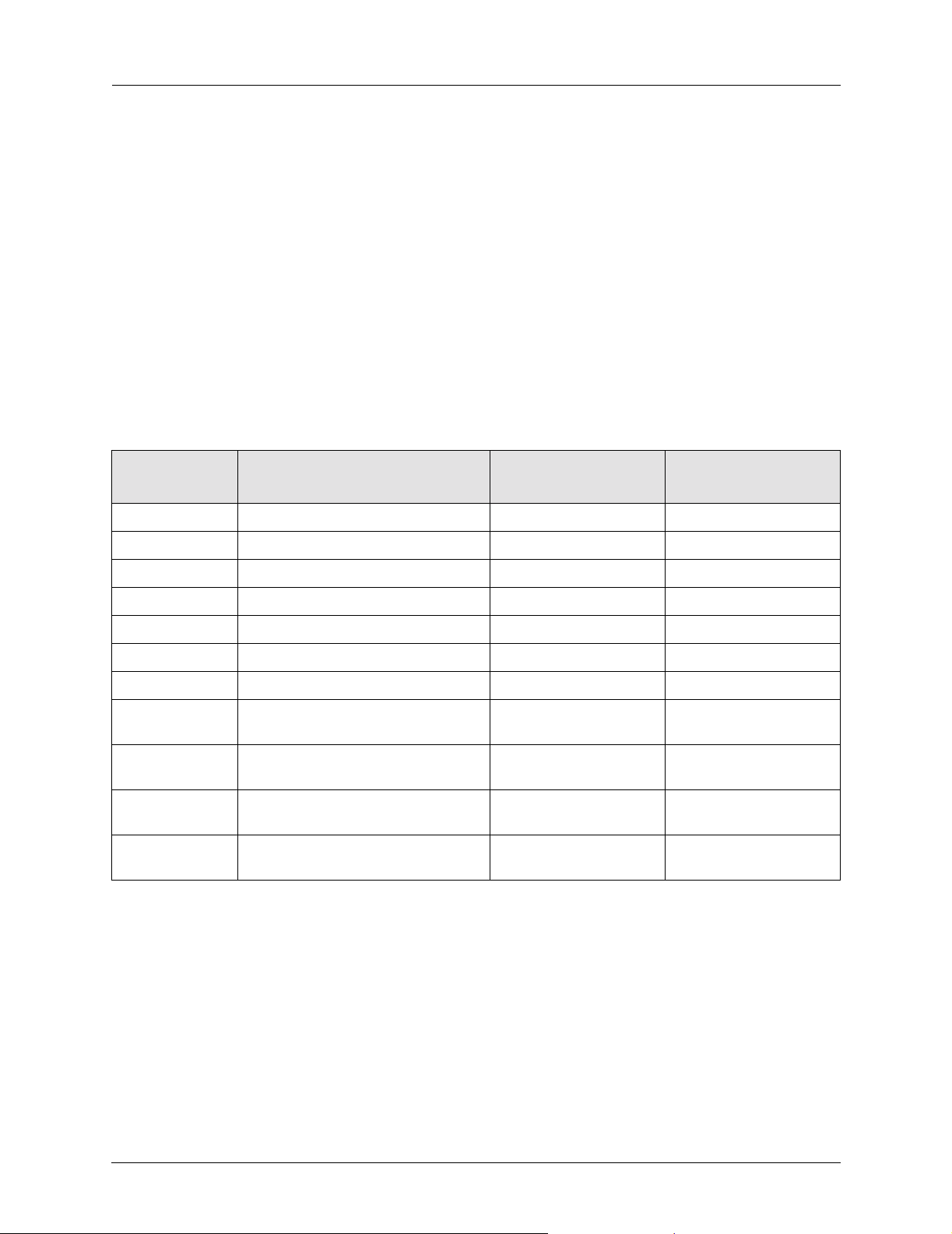
Functional Description CX23880/CX23881/CX23882/CX23883 Data Sheet
2.4.9 PCI Data Streaming
The CX2388x uses the resources in the PCI Subsystem to stream data between its
peripherals and the host processor, across the PCI bus. A total of 12 streams of data
are supported, and can be active simultaneously, though the typical application
scenario will use a subset of the streams. The streams are independent from each other
and are controlled on an individual basis. There are two types of data stream channels,
namely downstream and upstream. A downstream channel transfers data from a
peripheral to the host memory using the PCI bus. An upstream channel transfers data
from the host memory to a peripheral using the PCI bus. High performance internal
data paths and programmable depth FIFOs are used to optimize the throughput of data
across the PCI bus. The programmable depth FIFOs, which are implemented using the
internal SRAM, de-couple the constant rate flow of peripheral data from the bursts
and latencies of the PCI bus. The channels have been assigned an arbitrary number
that is used for identification. Table 2-24 shows the channel information.
D
Table 2-24. MA Channel Assignment
Channel
Number
21 Video packed or planar Y (luminance) down 48
22 Video planar U (chrominance) down 6
23 Video planar V (chrominance) down 6
24 Video VBI (vertical blanking interval data) down 36
25 Audio (from audio decoder) down 0.2
26 Audio (to digital-analog converters) up 0.2
28 Transport Stream (MPEG) down 9
29 VIP Host (from Video Interface Port
peripheral)
30 VIP Host (to Video Interface Port
peripheral)
31 GP Host (from General Purpose Host
peripheral)
32 GP Host (to General Purpose Host
peripheral)
Purpose Type BW
down 6.5
up 6.5
down 6.5
up 6.5
max (MHz)
2-58 Conexant 101069A
Preliminary Information/Conexant Proprietary and Confidential 08/26/02
Page 89

CX23880/CX23881/CX23882/CX23883 Data Sheet Functional Description
2.4.10 SRAM
The CX2388x contains an internal 32 Kbyte SRAM that is used to store data and
control information for the active streams. The usage of the SRAM is programmable
to accommodate a wide range of application scenarios. For example, an application
can implement larger FIFOs on high bandwidth streams and smaller FIFOs on low
bandwidth streams to handle the transfer latencies that may be encountered on the PCI
bus. A multiple stream application may ha ve some streams that are more tolerant to
occasional data loss than others. The more critical streams can use deeper FIFOs,
while the more tolerant streams can use smaller FIFOs. In addition to the FIFOs, the
SRAM is used for control information, namely, RISC instruction queues, Channel
Management Data Structures (CMDS), and optionally RISC programs. For each
application, the FIFO depth for each stream is programmable, with the obvious
restriction that the SRAM space used for the FIFOs plus the control information for
all the active streams, cannot exceed 32 Kbytes.
2.4.11 FIFO Size Calculation
FIFOs are used to decouple the constant data rate stream and the burst transfer nature
of the PCI bus. Though the PCI bus has sufficient avera ge bandwidth to accommo date
the demands of the peripherals, latencies can exist that are significant and can cause
loss of peripheral data if no buffering were provided. The amount of FIFO buffering
required depends on the average bandwidth of the peripheral data and the duration of
PCI latencies to be tolerated. Latencies encountered on PC systems are usually in the
10-20 microsecond range, with occasionally longer latencies of 100-200
microseconds. By sizing the FIFO buffers properly, most applications will be able to
protect its streams from the PCI latencies that are commonly encountered. The
amount of buffering is the multiplication product of the a v erage band width of the data
stream and the PCI latency duration.
The following is an example calc ulati on of the FIFO buffer required for a video PAL,
768 pixel x 576 lines, RGB16 stream to tolerate a 200 microsecond PCI latency. The
data stream bandwidth would be 24 Mbytes per second (25 frames per second * 625
total lines per frame * 768 pixels per line * 2 bytes per pixel = 24 Mbytes per second).
The amount of FIFO buffering required would be 4800 bytes (24 Mbytes per second *
200 microseconds = 4800 bytes). Since the FIFO buffer must be a multiple number of
lines and be two or greater, the FIFO buffer would actuall y be 61 44 bytes (4800 bytes
/ 2 bytes per pix el / 76 8 pix els per line = 3.125 lines, rou nded up to 4 lin es * 768 pix els
per line * 2 bytes per pixel = 6144 bytes). The actual latency protection would be 256
microseconds (6144 bytes / 24 Mbytes per second = 256 microseconds). Rounding
down to 3 lines would require only 4608 bytes (3 lines * 768 pixels per line * 2 bytes
per pixel = 4608 b ytes), which w ould provide latency protection of 192 microseconds
(4608 / 24 Mbytes per second = 192 microseconds).
The following is an example calculation of the FIFO buffer required for an ATSC
MPEG transport stream (2.5 Mbytes per second) to tolerate a 200 microsecond PCI
latency. The artificial line length is arbitrary, and the value chosen will affect the size
of the FIFO as it must be a multiple number of lines. This example will be done using
an artificial line length of 4 MPEG packets, which is 752 b y tes (4 p ack ets * 18 8 bytes
per packet). The amount of FIFO buffering required would be 500 bytes (2.5 Mbytes
per second * 200 microseconds = 500 bytes). Since the FIFO buffer must be a
multiple number of lines and must two or greater, the FIFO buffer would actually be
1504 bytes (752 bytes per line * 2 lines = 1504 bytes). The actual latency protection
would be 601.6 microseconds (1504 bytes / 2.5 Mbytes per second = 601.6
microseconds).
101069A Conexant 2-59
08/26/02 Preliminary Information/Conexant Proprietary and Confidential
Page 90

Functional Description CX23880/CX23881/CX23882/CX23883 Data Sheet
2.4.12 Programmable FIFO
A programmable FIFO is implemented in the SRAM using a number of equal sized
buffers, known as Cluster Buffers, and a table of pointers to the buffers, known as a
Cluster Descriptor Table. The number of buffers and the size of the buffers are
programmable, and are chosen based on the depth of the FIFO needed. For example, if
a 1 Kbyte FIFO is needed for a stream, it could be implemented using 4, 256 byte
buffers. A diff erent st ream could have a 1 Kbyte FIFO implemented using 8, 128 b yte
buffers.
Though the number and size of the buffers are programmable, there are a few
restrictions. The number of buffers must be two or greater. This allows the peripheral
to be streaming data to or from a buffer, while the PCI DMA controller bursts data to
or from a different buffer. Each buffer must large enough to accommodate one and
only one line of peripheral data, and be an integer number of qwords (8 bytes). For
video streams, the line size is dependen t on the video fo rmat. F or exa mple, a 768 pix el
x 576 line, RGB32 format would have 3 Kbyte lines. The other downstream
peripherals are not inherently line based and therefore use an artificial line length
chosen by the application. For example, an MPEG Transport Stream may chose a line
length equal to four packets, which would be 752 bytes (4x 188 bytes).
T o specify the buffer size, use the DMAx_CNT1 register, where x is the number of the
stream from Table 2-24. The register is written with the number of qwords minus one.
For example, to specify 3 Kbytes as the size of the buffers for the packed video
stream, write 11’h17F to the DMA21_CNT1 register. To specify the buffer locations,
use the Cluster Descriptor Table as described in the following paragraphs.
The set of buffers that make up a FIFO are supported by a Cluster Descriptor Table
(CDT), which is also located in the SRAM. The table con tains a four dw ord de scriptor
for each buffer, therefore the size of the CDT is directly related to the number of
buffers that make up the FIFO. For example, a FIFO that was made up of three buffers
would have a three entry table which would be a total of 48 bytes. The first dword of
each entry is the address of the beginning of the buffer. The address is a 24-bit SRAM
address (24’h18xxxx) and must be dword aligned. The other three dwords of each
descriptor are reserved for use by the internal hardware.
To specify the CDT size, use the DMAx_CNT2 register, where x is the number of the
stream from Table 2-24. The register is written with the number of qwords. For
example, to specify 48 bytes as the size of the CDT for the pack ed video stream, write
11’h006 to the DMA21_CNT2 register. This value must also be written to the Cluster
Descriptor Table Size field in the Channel Management Data Structure (CMDS).
To specify the SRAM location of the CDT, use the DMAx_PTR2 register, where x is
the number of the stream from Table 2-24. The register is written with the 24-bit
SRAM address (24’h18xxxx) and must be dw ord align ed . For example, to specify
15’h1000 as the CDT location for the packed video stream, write 24’h181000 to the
DMA21_PTR2 register. This value must also be written to the Cluster Descriptor
Table Base field in the Channel Management Data Structure (CMDS).
T o specify the SRAM locations of the buf fers, use the first dword of each descriptor in
the CDT. The register is written with the 24-bit SRAM address (24’h18xxxx) and
must be dword aligned. For example, to specify the SRAM locations for the start of
three, 3 Kbyte buffers to be 15’h2000, 15’h2C00, and 15’h3800, using a CDT that is
located at 15’h1000, write 24’h182000 to 24’h181000, 24’h182C00 to 24’h181010,
and 24’h183800 to 24’h181020.
The CDT and buffers can be located an yw here in the SRAM with the e xception of the
address range 15’h0000 to 15’h033F, which is reser ved for the Channel Management
Data Structures.
2-60 Conexant 101069A
Preliminary Information/Conexant Proprietary and Confidential 08/26/02
Page 91

CX23880/CX23881/CX23882/CX23883 Data Sheet Functional Description
2.4.13 RISC Instruction Queue
The CX2388x DMA architecture includes a RISC controller, which is programmed
using a simple set of RISC instructions. A series of RISC instructions form a program
that specifies the PCI target addresses and the amount of data to be read or written by
the CX2388x DMA controller. The RISC programs are generated by the software
driver on the host and are stored either in host memory or in CX2388x SRAM. Each
active stream implements a RISC instruction queue in the SRAM to maximize the
flow of instructions from the program memory to the RISC controller . When the RISC
controller has no other higher priority task to attend to, such as transferring stream
data, it will attempt to keep the instruction queue full. This increases the system
performance as the RISC controller will virtually always have the next instruction
ava ilab le in SRAM w hen it needs it, and will not have to w ait until it can fetch it from
the host memory. The inst ruction queues are programmable in siz e and location in the
SRAM. The minimum size is 8 dwords, the maximum size is 255 dwords, and the
typical size is 16 dwords. Use the Instruction Queue Base and Instruction Queue Size
fields in the Channel Management Data Structure (CMDS) to specify the location and
size. The address must be dword aligned, and the size is in dwords. For example, to
specify the packed video instruction queue to be 16 dwords in size and begin at
address 15’h0400 in the SRAM, write 24’h180400 to address 24’h18004C, and write
8’h10 to address 24’h180050. See Figure 2-22 for an example.
101069A Conexant 2-61
08/26/02 Preliminary Information/Conexant Proprietary and Confidential
Page 92

Functional Description CX23880/CX23881/CX23882/CX23883 Data Sheet
Figure 2-22. SRAM Resource Example
Registers
DMA21_PTR2
24'h18100024'h3000C0
DMA21_CNT2
11'h00624'h300140
DMA21_CNT1
11'h17F24'h300100
CMDS
Instruction
Queue
CDT
24'h180000
24'h18003F
24'h180040
24'h180044
24'h180048
24'h18004C
24'h180050
24'h18033F
24'h180400
24'h18403F
24'h181000
24'h181004
24'h181008
24'h18100C
24'h181010
24'h181014
24'h181018
24'h18101C
24'h181020
24'h181024
24'h181028
24'h18102C
SRAM
Reserved
24'h181000
11'h006
24'h180400
8'h10
Unused
Unused
24'h182000
Reserved
24'h182C00
Reserved
24'h183800
Reserved
Unused
24'h182000
Buffer 1
24'h182BFF
24'h182C00
Buffer 2
24'h1837FF
24'h183800
Buffer 3
24'h1843FF
Unused
24'h187FFF
101069_087
2-62 Conexant 101069A
Preliminary Information/Conexant Proprietary and Confidential 08/26/02
Page 93
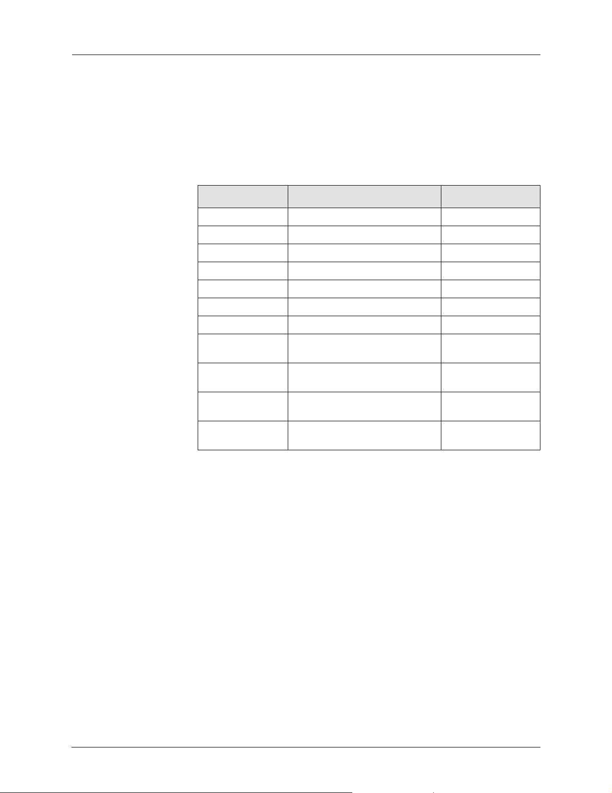
CX23880/CX23881/CX23882/CX23883 Data Sheet Functional Description
2.4.14 Channel Management Data Structure
The CX2388x uses the SRAM to store information to manage each stream channel.
This information is called the Channel Management Data Structure (CMDS) and is
fixed in the SRAM from address 15’h0040 to 15’h033F. The CMDS for each channel
is located in the SRAM as shown in Table 2-25.
Table 2-25. Channel Management Data Structure
Number Purpose CMDS Base
21 Video packed or planar Y (luminance) 15’h0040
22 Video planar U (chrominance) 15’h0080
23 Video planar V (chrominance) 15’h00C0
24 Video VBI (vertical blanking interval data) 15’h0100
25 Audio (from audio decoder) 15’h0140
26 Audio (to digital to analog converters) 15’h0180
28 Transport Stream (MPEG) 15’h0200
29 VIP Host (from Video Interface Port
peripheral)
30 VIP Host (to Video Interface Port
peripheral)
31 GP Host (from General Purpose Host
peripheral)
32 GP Host (to General Purpose Host
peripheral)
15’h0240
15’h0280
15’h02C0
15’h0300
101069A Conexant 2-63
08/26/02 Preliminary Information/Conexant Proprietary and Confidential
Page 94
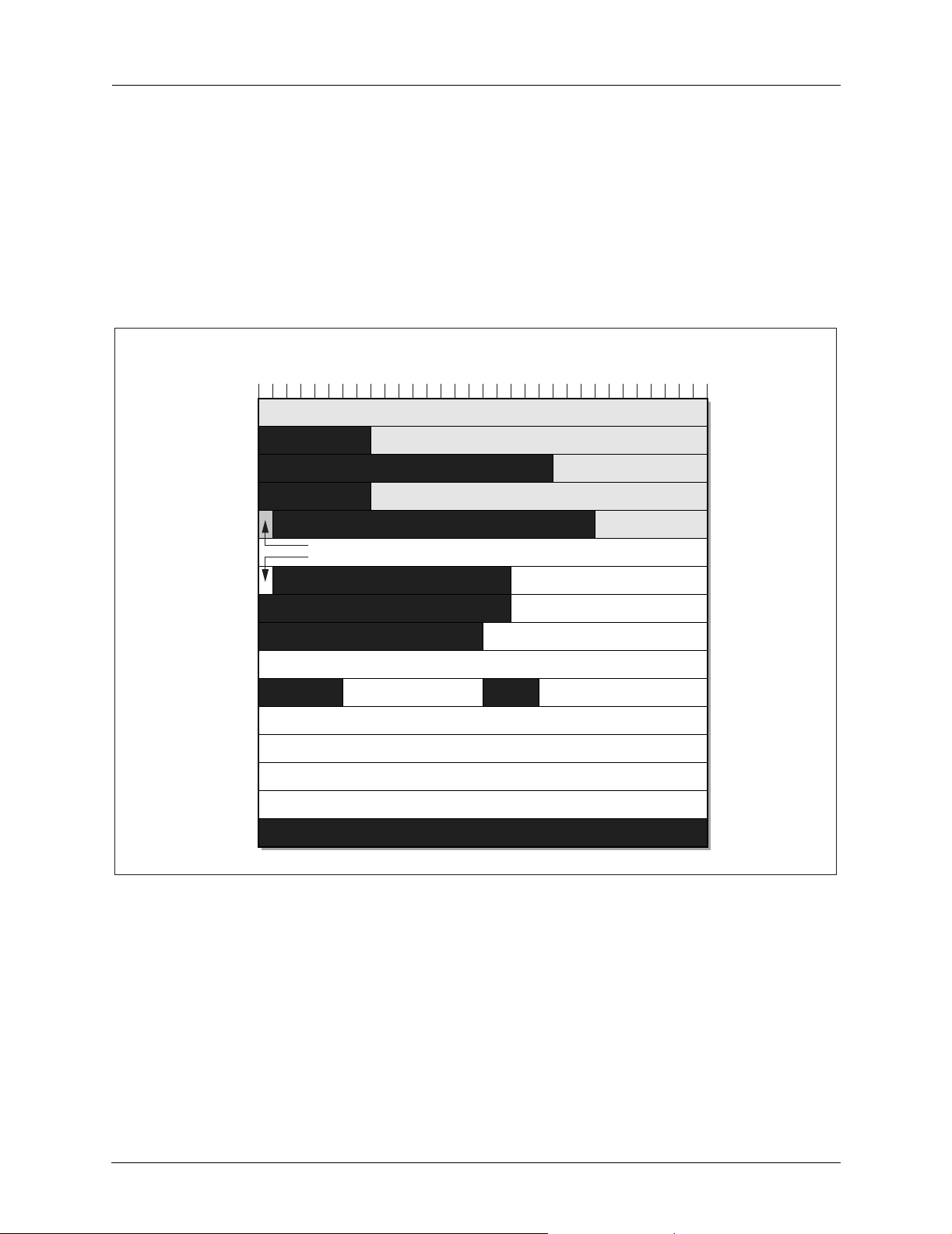
Functional Description CX23880/CX23881/CX23882/CX23883 Data Sheet
The CMDS is composed of 16 dwords. The first five dwords (shown in gray in
Figure 2-23) are information that is supplied by the host software to control and set up
the RISC controller. The ne xt ten dwords (shown in white in Figure 2-23) are used by
the RISC controller to manage the stream channel. These fields are not to be written
by the host software, though the y can be read to monitor the channel information. The
last dword (shown in black) is reserved and not used at this time, as are the rest of the
fields shown in black in Figure 2-23. This figure also shows the layout of the CMDS.
The fields of the CMDS are described in the next paragraph.
Figure 2-23. Channel Management Data Structure
Offset
6'h00
6'h04
6'h08
6'h0C
6'h10
6'h14
6'h18
6'h1C
6'h20
6'h24
6'h28
6'h2C
6'h30
6'h34
Channel Management Data Structure
24 16 8 0
Initial RISC Program Counter
CDT Base
Instruction Q Base
ISRP
SRP
Line Count Current Byte Count Current
RISC Instruction DWORD 0 Current
RISC Instruction DWORD 1 Current
RISC Instruction DWORD 2 Current
RISC Program Counter
Instruction Q Write Pointer
Instruction Q Read Pointer
CDT Current
PCI Target Address Current
CDT Size
Instruction Q Size
6'h38
6'h3C
2-64 Conexant 101069A
Preliminary Information/Conexant Proprietary and Confidential 08/26/02
RISC Instruction DWORD 3 Current
101069_086
Page 95

CX23880/CX23881/CX23882/CX23883 Data Sheet Functional Description
Initial RISC Program Counter[31:0]
Location of the first RISC instruction. In SRAM Resident Program mode (SRP =1),
this location will be an SRAM address, and only bits [23:0] are relevant. In PCI
Memory Resident Program mode (SRP = 0), it will be a PCI target address of the host
memory. The SRP bit is located at bit [31] in the dword at offset 6’h10.
CDT Base[23:0]
Location of beginning of the Cluster Descriptor Table in the SRAM. This address
must match the address written to the DMAx_PTR2 re gister , where x is the numbe r of
the stream from Table 2-24. See the description of the CDT in the Programmable
FIFOs section.
CDT Size[10:0]
The size in qwords of the CDT. This value must match the size written to the
DMAx_CNT2 register, where x is the number of the stream from Table 2-24. See the
description of the CDT in the Programmable FIFOs section.
Instruction Q Base[23:0]
Location of the beginning of the RISC instruction queue.
Instruction Q Size[7:0]
The size in dwords of the RISC instruction queue.
ISRP[31] (Initial SRAM Resident Program)
Used to specify whether the address in the Initial RISC Program Counter field is an
SRAM address (ISRP =1), or a PCI target address (ISRP = 0).
RISC Program Counter[31:0]
The RISC controller uses this as temporary storage for the address of the current
RISC instruction it is processing.
SRP[31] (SRAM Resident Program)
Used by the RISC controller to determine whether the program counter contains an
SRAM address (SRP =1), or a PCI target address (SRP = 0).
Instruction Q Write Pointer[13:0]
Used by the RISC controller to maintain the location of the next dword to be written.
This is a dword address, not a byte address.
101069A Conexant 2-65
08/26/02 Preliminary Information/Conexant Proprietary and Confidential
Page 96

Functional Description CX23880/CX23881/CX23882/CX23883 Data Sheet
Instruction Q Read Pointer[13:0]
Used by the RISC controller to maintain the location of the next dword to be read.
This is a dword address, not a byte address.
CDT Current[15:0]
The RISC controller uses this as temporary storage for the current entry in the CDT
that is being processed.
PCI Target Address Current[31:0]
The RISC controller uses this as temporary storage for the current PCI target address.
Byte Count Current[11:0]
The RISC controller uses this as temporary storage for the number of bytes of the
current line that have been processed.
Line Count Current[25:16]
The RISC controller uses this as temporary storage for the current line it is
processing.
RISC Instruction DWORD 0-3 Current[31:0]
The RISC controller uses this as temporary storage for the current instruction being
processed.
2.4.15 RISC Controller
The CX2388x DMA architecture includes a RISC controller, which coordinates the
transfer of data over the 12 stream channels. Though each channel has independent
control and data buffering, they are all handled by the single RISC controller. The
RISC controller is put into a rese t state whenever the CX2388x is reset. To allow the
RISC controller to operate the RUN_RISC bit[5] in the Device Control #2 register
must be set to one. The RISC controller can be returned to the reset state at any time
by clearing the RUN_RISC bit to zero.
2.4.16 RISC Instructions
The RISC controller processes a program made up of a series of RISC instructions.
The purpose of the RISC program is to specify the PCI target addresses and the
amount of data to be read or written by the CX2388x DMA controller. The RISC
programs are generated by the software driver on the host and are stored either in host
memory or in CX2388x SRAM. The address of the beginning of the program must be
written to the Initial RISC Program Counter field in the CMDS. When the channel is
turned on, the RISC controller will load the initial program counter into the program
counter and begin processing the instructions. Programs that are stored in the host
2-66 Conexant 101069A
Preliminary Information/Conexant Proprietary and Confidential 08/26/02
Page 97
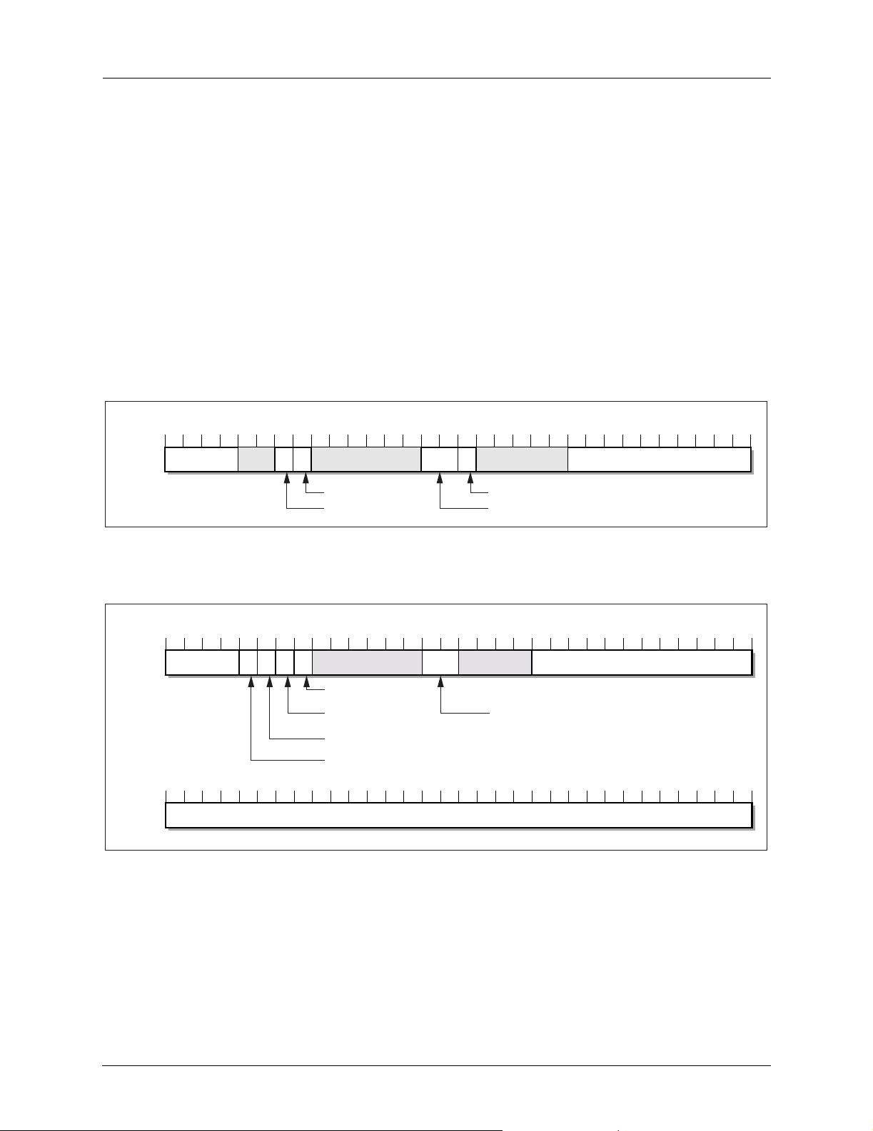
CX23880/CX23881/CX23882/CX23883 Data Sheet Functional Description
memory are called PCI Memory Resident Programs, while programs that are stored in
the CX2388x SRAM are called SRAM Resident Programs. To indicate whether the
address in the Initial RISC Program Counter is a PCI memory address or a CX2388x
SRAM address, the Initial SRAM Resident Program (ISRP) bit must be written. The
ISRP bit is bit [31] at offset 6’h10 in the CMDS. A PCI Memo ry Resident Pro gram is
specified by writing the ISRP bit to 0, an SRAM Resident Program is specified by
writing the ISRP bit to 1. See Figure 2-23, Channel Management Data Structure.
The RISC instruction set is composed of 10 instructions that can be categorized as
downstream, upstream, and common to both directions. The downstream instructions
are SYNC, WRITE, and WRITEC. The upstream instructions are READ and
READC. The instructions that can be used in both downstream and upstream
programs are JUMP, SKIP, WRITERM, WRITECM, and WRITECR. See
Figures 2-24 through 2-33 for RISC instruction specifics.
Figure 2-24. SYNC downstream RISC Instruction
2
2
4
5
IRQ2
SYNC
3
1
OPCODE
2
8
0001
Figure 2-25. WRITE downstream RISC Instruction
2
2
262
4
5
7
IRQ1
IRQ2
EOL
SOL
WRITE
3
1
0001
OPCODE
3
1
2
8
1
1
1
6
59
7
RESYNCIRQ1
CNT_CTL
1
1
6
7
CNT_CTL
PCI TARGET ADDRESS
0
LINE COUNT
101069_088
1
1
BYTE COUNT
0
0
101069_089
101069A Conexant 2-67
08/26/02 Preliminary Information/Conexant Proprietary and Confidential
Page 98
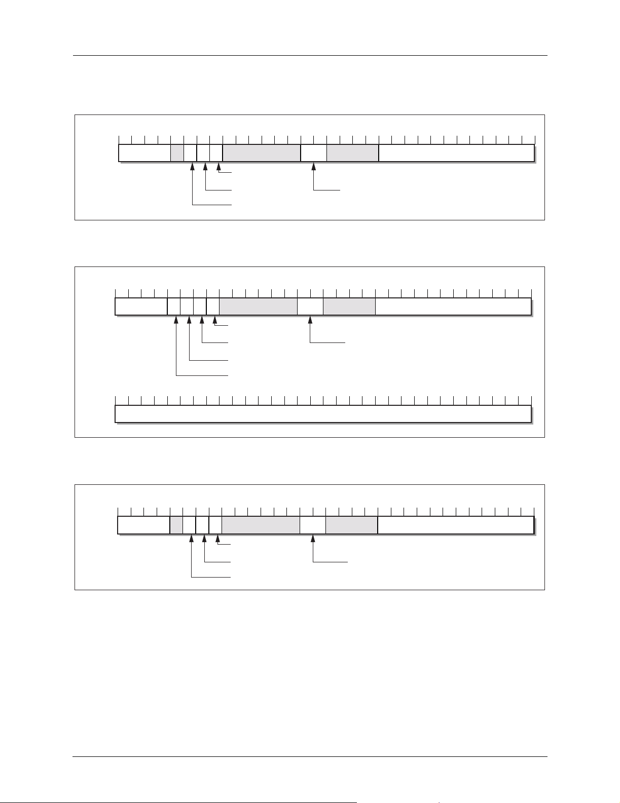
Functional Description CX23880/CX23881/CX23882/CX23883 Data Sheet
Figure 2-26. WRITEC downstream RISC instruction
2
2
262
4
5
7
IRQ1
WRITEC
3
1
2
8
0011
OPCODE
IRQ2
EOL
Figure 2-27. READ upstream RISC Instruction
2
2
262
4
5
7
IRQ1
IRQ2
EOL
SOL
READ
3
1
1001
OPCODE
3
1
2
8
1
1
6
7
CNT_CTL
1
1
6
7
CNT_CTL
PCI TARGET ADDRESS
1
1
1
1
0
BYTE COUNT
101069_090
0
BYTE COUNT
0
Figure 2-28. READC upstream RISC Instruction
2
2
262
4
5
7
IRQ1
IRQ2
EOL
READC
3
1
1010
OPCODE
2
8
101069_091
1
1
6
7
1
1
0
BYTE COUNT
CNT_CTL
101069_092
2-68 Conexant 101069A
Preliminary Information/Conexant Proprietary and Confidential 08/26/02
Page 99
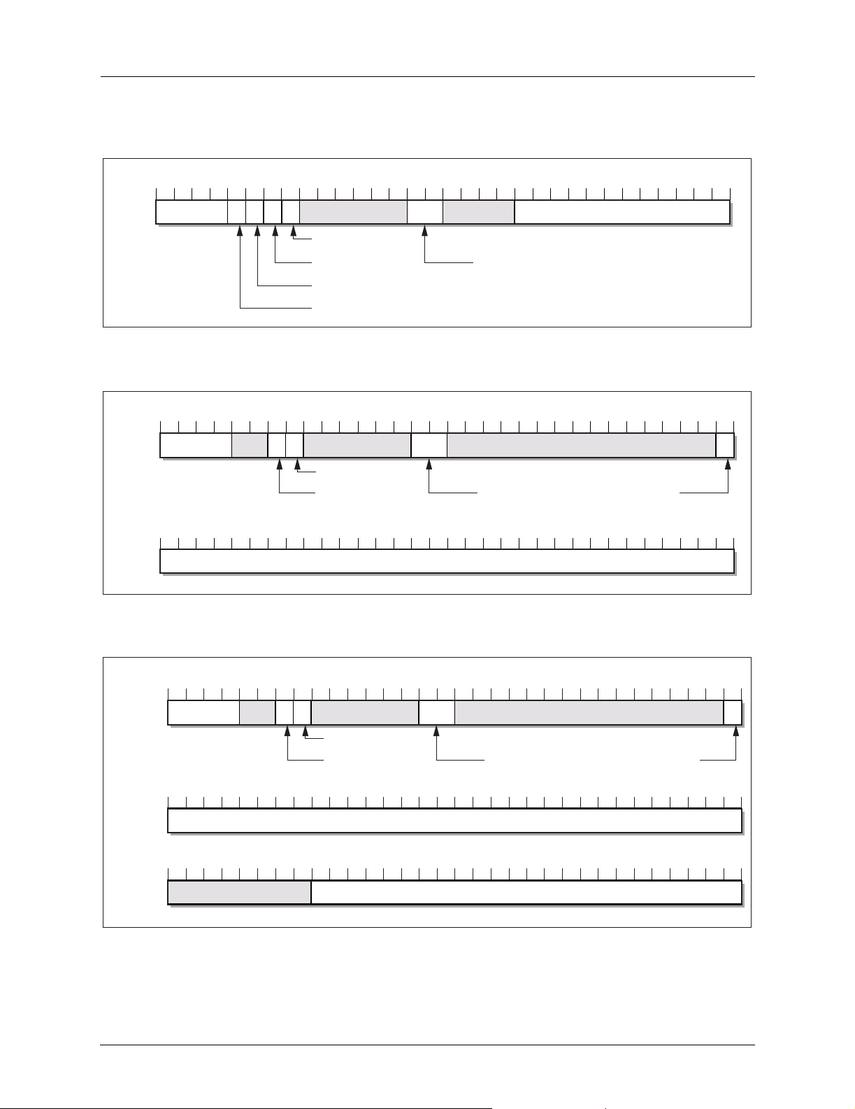
CX23880/CX23881/CX23882/CX23883 Data Sheet Functional Description
Figure 2-29. SKIP RISC Instruction
262
2
5
7
SKIP
3
1
2
8
0010
OPCODE
Figure 2-30. Jump RISC Instruction
2
5
JUMP
3
1
0111
OPCODE
3
1
2
8
2
4
1
1
6
7
1
1
0
BYTE COUNT
IRQ1
IRQ2
CNT_CTL
EOL
SOL
101069_093
2
4
1
1
6
7
0
IRQ1
IRQ2
CNT_CTL
SRP
2
3
0
JUMP ADDRESS
Figure 2-31. WRITERM RISC Instruction
2
2
4
5
2
4
WRITERM
3
1
1011
OPCODE
3
1
3
1
2
8
2
3
IRQ1
IRQ2
1
1
6
7
CNT_CTL
PCI TARGET ADDRESS
REGISTER ADDRESS
101069_094
0
1
IMM
0
0
101069_095
101069A Conexant 2-69
08/26/02 Preliminary Information/Conexant Proprietary and Confidential
Page 100
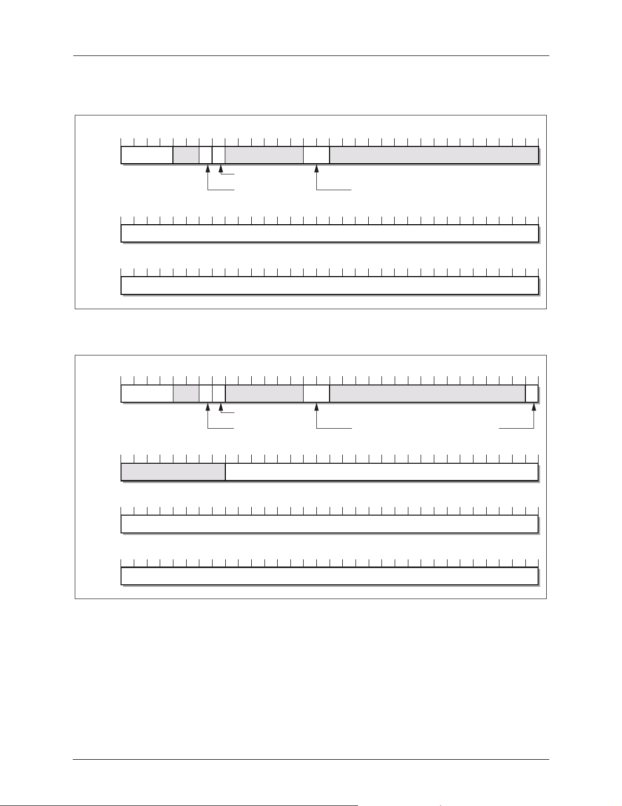
Functional Description CX23880/CX23881/CX23882/CX23883 Data Sheet
Figure 2-32. WRITECM RISC Instruction
2
2
4
5
WRITECM
3
1
1100
OPCODE
3
1
3
1
2
8
Figure 2-33. WRITECR RISC Instruction
2
2
4
5
WRITECR
3
1
1101
OPCODE
2
8
IRQ1
IRQ2
IRQ1
IRQ2
1
1
6
7
CNT_CTL
PCI TARGET ADDRESS
CONSTANT
1
1
6
7
CNT_CTL
0
0
0
101069_096
0
1
IMM
3
1
3
1
3
1
2
2
3
4
REGISTER ADDRESS
CONSTANT
MASK
0
0
0
101069_097
All instructions contain two interrupt bits, IRQ1 and IRQ2, that can be used to set the
RISCI1 and RISCI2 bits respectively, in the inter rupt status register of the
corresponding function. This allows a PCI interrupt to be generated when the
instruction is executed by the RISC controller. All instructions have control bits for
the general purpose counter associated with each channel. This allows the software
driver to count RISC program events. The two bit CNT_CTL field is coded for the
following action: 2’b00 = no change, 2’b01 = increment, 2’b10 = reserved,
2’b11 = reset to zero.
2-70 Conexant 101069A
Preliminary Information/Conexant Proprietary and Confidential 08/26/02
 Loading...