

Page 1

SDM-300A
Satellite Modem
Installation and Operation Manual
Part Number MN/SDM300A.IOM Revision 6
Page 2

Page 3

Errata A
Comtech EF Data Documentation Update
Subject:
Date:
Document:
Part Number:
Collating Instructions:
Comments:
Change paragraphs A. 1and A.2 are highlighted to read:
Change Specifics:
Appendix A. Remote Control Operation
June 21, 2005
SDM-300A Satellite Data Modem Installation and Operation
Manual, Rev. 4, dated June 15, 2000
MN/SDM300A.EA6
Attach this page to page A-1
A.1 General
Remote control and status information is transferred via a RS-485 or RS-232 serial
communications link. Commands and data are transferred on the remote control communications
link as US ASCII encoded character strings. The remote communications link is operated in a half
duplex mode. A remote controller or terminal initiates communications on the remote link. The
SDM300A never transmits data on the link unless it is commanded to do so.
A.2 Message Structure
The ASCII character format requires 11 bits/character: 1 start bit, 7 information bits with 1 parity bit
(odd/even) or 8 information bits with no parity bits, and 2 stop bits.
Messages on the remote link fall into the categories of commands and responses. Commands are
messages transmitted to a satellite modem, while responses are messages returned by a satellite
modem in response to a command.The general message structure is as follows:
• Start Character ‘<’
• Device Address 'add'
• Address De-limiter ‘/’
• Command/Response
• Qualifier ‘_’
• Optional Arguments ‘n, m, x, y, z’
• End of Message Character
Filename: T_ERRATA 1
Page 4

Comtech EF Data Documentation Update
Subject:
Date:
Document:
Part Number:
Collating Instructions:
Comments:
Change paragraph 4.1.1 to read:
Change Specifics:
Correct RS reference in 4.1.1 Remote Connector and Pinouts (J6)
June 21, 2005
SDM-300A Satellite Data Modem Installation and Operation
Manual, Rev. 6, dated June 7, 2004
MN/SDM300A.EB6
Attach this page to page 4-4
Errata B
4.1.1 Remote Connector and Pinouts (J6)
The remote connector is a 9-pin subminiature female D connector (J6) located on the rear panel of
the modem. Screw locks are provided for mechanical security of the mating connector.
The remote connector interfaces the M&C functions to a remote location. The remote location can
be an M&C computer located away from the modem, but attached via cable to the remote
connector. This DCE interface is user selectable for either RS-232 or RS-485. Refer to Appendix A
for a description of the remote interface commands.
Filename: T_ERRATA 1
Page 5

Comtech EF Data is an ISO 9001
Registered Company.
SDM-300A
Satellite Modem
Installation and Operation Manual
Part Number MN/SDM300A.IOM
Revision 6
June 7, 2004
Copyright © Comtech EF Data, 2000, 2001, 2002. All rights reserved. Printed in the USA.
Comtech EF Data, 2114 West 7th Street, Tempe, Arizona 85281 USA, 480.333.2200, FAX: 480.333.2161.
Page 6

Customer Support
Contact the Comtech EF Data Customer Support Department for:
• Product support or training
• Information on upgrading or returning a product
• Reporting comments or suggestions concerning manuals
A Customer Support representative may be reached at:
Comtech EF Data
Attention: Customer Support Department
2114 West 7th Street
Tempe, Arizona 85281 USA
480.333.2200 (Main Comtech EF Data Number)
480.333.4357 (Customer Support Desk)
480.333.2161 FAX
or, E-Mail can be sent to the Customer Support Department at:
service@comtechefdata.com
Contact us via the web at www.comtechefdata.com
To return a Comtech EF Data product (in-warranty and out-of-warranty) for repair or
replacement:
1. Request a Return Material Authorization (RMA) number from the Comtech EF
Data Customer Support Department.
Be prepared to supply the Customer Support representative with the model
number, serial number, and a description of the problem.
2. To ensure that the product is not damaged during shipping, pack the product in
its original shipping carton/packaging.
3. Ship the product back to Comtech EF Data. (Shipping charges should be
prepaid.)
For more information regarding the warranty policies, see Warranty Policy, p. xv.
.
ii
Page 7

Table of Contents
Chapter 1. INTRODUCTION...................................................................................................................................1–1
1.1 Overview......................................................................................................................................................1–3
1.1.1
Modem Features ..................................................................................................................................1–3
1.1.2 Standard Features ...............................................................................................................................1–3
1.1.3 Description of Interface Functions........................................................................................................1–4
1.1.4 Modes of Operation..............................................................................................................................1–4
1.2 Options ........................................................................................................................................................1–6
1.2.1 Factory-Installed Options .....................................................................................................................1–7
1.2.2 Factory- or user-Installed Options ........................................................................................................1–7
1.3
Description of FAST Options.....................................................................................................................1–8
1.4
Compatibility ...............................................................................................................................................1–9
1.5
Breakout Panels..........................................................................................................................................1–9
1.5.1 UB-300 Universal Breakout Panel........................................................................................................1–9
1.5.2 UB-530 Breakout Panel........................................................................................................................1–9
UB-54 Breakout Panel .......................................................................................................................1–10
1.5.3
1.6 Comtech EF Data Part Numbers..............................................................................................................1–10
1.7 New in this Release ..................................................................................................................................1–13
CHAPTER 2.
2.1 Description of Monitor and Control (M&C) ...............................................................................................2–1
2.1.1
2.1.2 Remote Baud Rate...............................................................................................................................2–4
2.1.3
FUNCTIONAL DESCRIPTION....................................................................................................2–1
Theory of Operation .............................................................................................................................2–1
Remote Address ..................................................................................................................................2–4
iii
Page 8

SDM-300A Satellite Modem Revision 6
Preface MN/SDM300A.IOM
2.2 Decription of the Modulator .......................................................................................................................2–5
2.2.1
Theory of Operation .............................................................................................................................2–6
2.2.2 Theory of Modulation Types.................................................................................................................2–7
2.3 Description of the Demodulator ................................................................................................................2–8
2.4 Description of the Decoder ......................................................................................................................2–10
2.5 Description of the Interface .....................................................................................................................2–11
2.5.1
Available Interfaces............................................................................................................................2–13
2.5.2 Plesiochronous/Doppler/Buffer...........................................................................................................2–13
2.5.3 Closed Network..................................................................................................................................2–14
2.5.4 Open Network ....................................................................................................................................2–14
2.6 Backward Alarm Theory and Connections.............................................................................................2–15
CHAPTER 3.
3.1 Unpacking....................................................................................................................................................3–1
3.2 Installation...................................................................................................................................................3–2
3.3 Software and Hardware Installation/Upgrades.........................................................................................3–4
3.3.1 Overhead Interface PCB Installation ....................................................................................................3–4
3.3.2 Hardware Upgrades .............................................................................................................................3–6
3.4
Reed-Solomon PCB ....................................................................................................................................3–6
3.4.1 Unpacking ............................................................................................................................................3–6
3.4.2 Installation............................................................................................................................................3–6
3.5
Turbo Codec Installation............................................................................................................................3–8
3.5.1 Unpacking ............................................................................................................................................3–8
3.5.2 Installation............................................................................................................................................3–9
3.6
Duplex Reed-Solomon Codec Installation..............................................................................................3–13
3.7 Data I/O Interface Connector (J8) Removal/Installation ........................................................................3–17
3.7.1 Data I/O Connector (J8) Removal ......................................................................................................3–17
3.7.2 Data I/O Connector (J8) Installation ...................................................................................................3–18
INSTALLATION/UPGRADES.....................................................................................................3–1
3.8
Hardware Upgrades ..................................................................................................................................3–20
3.8.1 Main PCB Firmware Chips.................................................................................................................3–20
3.8.2 Overhead Interface PCB ....................................................................................................................3–22
iv
Page 9

SDM-300A Satellite Modem Revision 6
Preface MN/SDM300A.IOM
CHAPTER 4. EXTERNAL CONNECTIONS......................................................................................................4–1
4.1 External Modem Connections....................................................................................................................4–1
4.1.1 Remote Connector and Pinouts (J6) ....................................................................................................4–4
4.1.2 Fault Connector and Pinouts (J7).........................................................................................................4–5
4.1.3 Data I/O Interface Connector (J8) ........................................................................................................4–6
4.1.4 G.703 ASYNC Interface .....................................................................................................................4–12
4.1.5 Auxiliary 1 Connector and Pinouts (J9) ..............................................................................................4–13
4.1.6 Alarms Connector and Pinouts (J10) .................................................................................................4–14
4.1.7 RF Output Connector (CP1)...............................................................................................................4–14
4.1.8 RF Input Connector (CP2)..................................................................................................................4–14
4.1.9 External Reference (CP3) ..................................................................................................................4–15
4.1.10 Power Entry........................................................................................................................................4–15
4.1.11 Ground Connector (GND) ..................................................................................................................4–15
CHAPTER 5. FRONT PANEL OPERATION.....................................................................................................5–1
5.1
Front Panel ..................................................................................................................................................5–1
5.1.1 LED Indicators......................................................................................................................................5–2
5.1.2 Front Panel Keypad .............................................................................................................................5–3
5.2 Menu System...............................................................................................................................................5–4
5.3
Revision Emulation Operation...................................................................................................................5–5
5.4 Opening Screen ..........................................................................................................................................5–7
5.4.1 Functional Select: Configuration ..........................................................................................................5–7
5.4.1.1 Functional Select: Configuration: Modulator................................................................................5–8
5.4.1.2 Functional Select: Configuration: Demodulator ........................................................................5–14
5.4.1.3 Functional Select: Configuration: Interface................................................................................5–22
5.4.1.4 Functional Select: Configuration: Local AUPC ..........................................................................5–42
5.4.1.5 Functional Select: Configuration: Mux ......................................................................................5–47
5.4.1.6 Functional Select: Configuration: Flex Mux ...............................................................................5–49
5.4.1.7 Functional Select: Configuration: Save .....................................................................................5–55
5.4.1.8 Functional Select: Configuration: Recall....................................................................................5–55
5.4.2
Functional Select: Monitor..................................................................................................................5–56
5.4.3 Functional Select: Faults/Alarms........................................................................................................5–60
5.4.4 Functional Select: Stored FLTS/ALMS...............................................................................................5–65
5.4.5 Functional Select: Remote AUPU (Conditional).................................................................................5–69
5.4.6
Functional Select: Utility.....................................................................................................................5–74
5.4.6.1 Functional Select: Utility: Fixed Modem Rate............................................................................5–74
5.4.6.2 Functional Select: Utility: Fixed Modem Rate: Code Rate/Data Rate .......................................5–74
5.4.6.3 Functional Select: Utility: Modulator ..........................................................................................5–75
5.4.6.4 Functional Select: Utility: Demodulator .....................................................................................5–80
5.4.6.5 Functional Select: Utility: Interface ............................................................................................5–84
5.4.6.6 Functional Select: Utility: System ..............................................................................................5–92
5.4.6.7 Functional Select: Utility: Modem Type ....................................................................................5–99
v
Page 10

SDM-300A Satellite Modem Revision 6
Preface MN/SDM300A.IOM
5.4.6.8 Utility: Factory Set-Up..............................................................................................................5–109
5.5
Custom Modem Defaults........................................................................................................................5–110
CHAPTER 6. MODEM TYPES..........................................................................................................................6–1
6.1
Modem Types..............................................................................................................................................6–1
6.1.1 IDR Operation ......................................................................................................................................6–2
6.1.2 IBS Operation.......................................................................................................................................6–3
6.1.3 D&I Operation ......................................................................................................................................6–4
6.1.4
ASYNC/AUPC Operation .....................................................................................................................6–5
6.1.5 EFD Closed Network Configuration .....................................................................................................6–6
6.1.6 Custom Operation ................................................................................................................................6–7
6.1.7 SDM-100 Emulation Operation ............................................................................................................6–8
6.1.8 SDM-6000 Emulation Operation ..........................................................................................................6–9
6.2 Reed-Solomon Modes ..............................................................................................................................6–10
CHAPTER 7. CLOCKING OPTIONS ................................................................................................................7–1
7.1 Clocking Options ........................................................................................................................................7–1
7.1.1 EIA-232, EIA-422, or V.35 Master/Master............................................................................................7–1
7.1.2 EIA-232, EIA-422, or V.35 Master/Slave..............................................................................................7–1
7.1.3 IDR/IBS G.703 Master/Master..............................................................................................................7–2
7.1.4 IDR/IBS G.703 Master/Slave................................................................................................................7–2
7.1.5 D&I G.703 Master/Master.....................................................................................................................7–7
CHAPTER 8. BUFFERING................................................................................................................................8–1
8.1 Buffering ......................................................................................................................................................8–1
8.2
Buffer Size ...................................................................................................................................................8–4
8.3 Doppler ........................................................................................................................................................8–4
8.4
Plesiochronous...........................................................................................................................................8–5
8.5 Frame/Multiframe Length ...........................................................................................................................8–6
8.5.1
Multiples of the Frame Length..............................................................................................................8–6
8.5.2 Total Buffer Length...............................................................................................................................8–6
8.6 Converting Between Bits and Seconds ....................................................................................................8–6
8.6.1
Bits to Seconds..................................................................................................................................8–6
8.6.2 Seconds to Bits ....................................................................................................................................8–6
vi
Page 11

SDM-300A Satellite Modem Revision 6
Preface MN/SDM300A.IOM
CHAPTER 9. FORWARD ERROR CORRECTION (OPTIONS) .......................................................................9–1
9.1 Introduction .................................................................................................................................................9–1
9.2
Viterbi...........................................................................................................................................................9–2
9.3 Sequential....................................................................................................................................................9–3
9.4
Reed-Solomon Outer Codec ......................................................................................................................9–4
9.4.1
Closed Network Modes ........................................................................................................................9–5
9.4.2 Open Network Modes ..........................................................................................................................9–5
9.5 Trellis Coding (FAST Option).....................................................................................................................9–6
9.6
Turbo Product Codec (Hardware Option).................................................................................................9–7
Introduction.........................................................................................................................................9–7
9.6.1
9.6.2 End-to-End Processing Delay ..............................................................................................................9–7
Comparison of all TPC Modes.........................................................................................................9–8
9.6.3
9.7 Uncoded Operation (No FEC) ....................................................................................................................9–9
CHAPTER 10. OPEN NETWORK OPERATIONS ............................................................................................10–1
10.1 Introduction...............................................................................................................................................10–1
10.2
Intelsat Business System (IBS) ...............................................................................................................10–1
10.2.1 IBS Specification ................................................................................................................................10–4
10.2.2 IBS Modem Defaults ..........................................................................................................................10–5
10.2.3 IBS Primary Data Interface.................................................................................................................10–6
10.2.4 IBS Clock and Dejitter ........................................................................................................................10–6
10.2.5 IBS Framing .......................................................................................................................................10–6
10.2.6 IBS Engineering Service Channel......................................................................................................10–6
10.2.7 IBS Scrambling ..................................................................................................................................10–6
10.3 Intermediate Data Rate (IDR)....................................................................................................................10–7
10.3.1 IDR Specification..............................................................................................................................10–10
10.3.2 IDR Modem Defaults........................................................................................................................10–11
10.3.3 IDR Primary Data Interface ..............................................................................................................10–12
10.3.4 IDR Framing.....................................................................................................................................10–12
10.3.5 IDR Engineering Service Channel....................................................................................................10–12
10.4 Drop and Insert (D&I)..............................................................................................................................10–13
10.4.1 D&I Specification..............................................................................................................................10–14
10.4.2 Theory of Operation .........................................................................................................................10–18
10.4.3 Data Interference .............................................................................................................................10–18
10.4.4 Transmitted MUX .............................................................................................................................10–18
10.4.5 Receive DEMUX ..............................................................................................................................10–19
10.4.6 Plesiochronous Buffer ......................................................................................................................10–19
10.4.7 Engineering Service Channel...........................................................................................................10–20
10.4.8 Backward Alarm ...............................................................................................................................10–20
vii
Page 12

SDM-300A Satellite Modem Revision 6
Preface MN/SDM300A.IOM
10.4.9 D&I Framing Formats.......................................................................................................................10–20
10.4.10 D&I Modem Defaults ........................................................................................................................10–23
10.4.11 D&I Primary Data Interface ..............................................................................................................10–24
10.4.12 D&I Framing.....................................................................................................................................10–24
10.5
G.703........................................................................................................................................................10–25
CHAPTER 11. ASYNCHRONOUS INTERFACE/AUPC...................................................................................11–1
11.1
Asynchronous Interface/AUPC................................................................................................................11–1
11.2
AUPC..........................................................................................................................................................11–4
11.2.1
AUPC - Between Two Modems..........................................................................................................11–5
11.2.2 Self-Monitoring Local Modem AUPC Control .....................................................................................11–6
11.3 ASYNC .......................................................................................................................................................11–7
11.3.1 Terrestrial Data Interfaces..................................................................................................................11–7
11.3.2 ASYNC Data Interfaces......................................................................................................................11–7
11.3.3 Mux Operation....................................................................................................................................11–8
11.3.4 Demux Operation ...............................................................................................................................11–8
11.3.5 Buffer Operation.................................................................................................................................11–8
11.3.6 LoopTiming Operation........................................................................................................................11–9
11.3.7
Baseband Loopback Operation..........................................................................................................11–9
11.3.8 Non-ASYNC Operation ....................................................................................................................11–10
11.4
ASYNC Channel EIA-485 2- and 4-Wire operation ...............................................................................11–10
11.4.1 Valid ASYNC Baud Rates ................................................................................................................11–11
11.4.2 Front Panel Operation......................................................................................................................11–11
11.4.3 ASYNC Remote Operation...............................................................................................................11–12
11.4.4 ASYNC/AUPC Modem Defaults.......................................................................................................11–24
CHAPTER 12. ASYMMETRICAL LOOP TIMING .............................................................................................12–1
CHAPTER 13.
CHAPTER 14. 8-CHANNEL MULTIPLEXER ...................................................................................................14–1
14.1 Introduction...............................................................................................................................................14–1
14.2 Installation.................................................................................................................................................14–2
14.3 8-Channel Multiplexer Specifications .....................................................................................................14–4
14.4
8-Channel Multiplexer 100-pin Connector (J10).....................................................................................14–5
DUPLEX REED-SOLOMON CODEC .......................................................................................13–1
viii
Page 13

SDM-300A Satellite Modem Revision 6
Preface MN/SDM300A.IOM
CHAPTER 15. FLEX MUX ................................................................................................................................15–1
15.1 Introduction...............................................................................................................................................15–1
15.2 Installation.................................................................................................................................................15–6
15.3 50-Pin Connector Assignments...............................................................................................................15–8
CHAPTER 16. FAST ACCESSIBLE OPTIONS ................................................................................................16–1
16.1 Introduction...............................................................................................................................................16–1
16.2 FAST Accessible Options ........................................................................................................................16–1
16.3 FAST System Theory................................................................................................................................16–3
16.4
Implementation .........................................................................................................................................16–3
16.5 Variable Data Rates ......................................................................................................................................16–6
CHAPTER 17.
CHAPTER 18. TROUBLESHOOTING ..............................................................................................................18–1
18.1 System Checkout......................................................................................................................................18–1
18.2
Interface Checkout....................................................................................................................................18–2
18.2.1
18.2.2 Demodulator Checkout ......................................................................................................................18–6
18.3 Fault Isolation............................................................................................................................................18–8
18.3.1 System Faults/Alarms ........................................................................................................................18–8
18.3.2 Faults/Alarms Display ......................................................................................................................18–12
18.3.3 Faults/Alarms Analysis.....................................................................................................................18–12
18.3.4
18.3.5 Remove and Replace the Fan Assembly .........................................................................................18–20
CHAPTER 19. SPECIFICATION.......................................................................................................................19–1
19.1 Specification Summary ............................................................................................................................19–1
Environmental and Physical Specifications...........................................................................................19–3
19.2
FLASH UPGRADING................................................................................................................17–1
Modulator Checkout ...........................................................................................................................18–3
Remove and Replace Power Supply................................................................................................18–19
19.3
Remote Control Specifications................................................................................................................19–4
19.4 Modulator Specifications .........................................................................................................................19–5
19.4.1
Digital Data Rate................................................................................................................................19–5
19.4.2 Modulation and Encoding Types ........................................................................................................19–7
19.4.3 Scrambling Types ..............................................................................................................................19–8
ix
Page 14

SDM-300A Satellite Modem Revision 6
Preface MN/SDM300A.IOM
19.4.4 Differential Encoder............................................................................................................................19–8
19.4.5 BPSK BIT Ordering ............................................................................................................................19–8
19.4.6 Interleaver (Reed-Solomon Codec)....................................................................................................19–8
19.4.7 Transmit Frequency (IF).....................................................................................................................19–9
19.4.8 Frequency Reference.........................................................................................................................19–9
19.4.9
Transmit Frequency Change Time.....................................................................................................19–9
19.4.10 Phase Noise.......................................................................................................................................19–9
19.4.11 Transmit IF Output Switch................................................................................................................19–10
19.4.12 Transmit IF Power............................................................................................................................19–10
19.4.13 Modulator Power Offset ...................................................................................................................19–10
19.4.14
19.4.15 Spurious Emissions..........................................................................................................................19–10
19.4.16 Modulator Phase Error .....................................................................................................................19–10
19.4.17 Transmit IF Test Modes ...................................................................................................................19–11
19.4.18 Modulator Spectrum Rotation...........................................................................................................19–11
19.5
19.5.1
19.5.2 Demodulation and FEC Decoding Types .........................................................................................19–13
19.5.3 Descrambling Types ........................................................................................................................19–14
19.5.4
19.5.5 BPSK BIT Ordering ..........................................................................................................................19–14
19.5.6 Deinterleaver (Reed-Solomon Codec) .............................................................................................19–15
19.5.7 Demodulator Spectrum Rotation ......................................................................................................19–15
19.5.8 Frequency Reference.......................................................................................................................19–15
19.5.9
19.5.10 Phase Noise.....................................................................................................................................19–15
19.5.11 Transmit IF Output Switch................................................................................................................19–15
19.5.12
19.5.13 Channel Spacing/Adjacent Carrier Performance..............................................................................19–16
Modulated IF Output Shape .............................................................................................................19–10
Demodulator Specifications...................................................................................................................19–12
Digital Data Rate..............................................................................................................................19–12
Differential Encoder..........................................................................................................................19–14
Transmit Frequency Change Time...................................................................................................19–15
Demodulator IF Input Shape ............................................................................................................19–16
19.6 BER Performance Specifications ..........................................................................................................19–16
19.6.1
Performance with Noise, Viterbi Decoder, and Open Network Mode...............................................19–17
19.6.2 Performance with Noise, Viterbi Decoder, and Closed Network ......................................................19–17
19.6.3 Performance with Noise, Viterbi Decoder, and Reed-Solomon (Optional).......................................19–18
19.6.4
Performance with Noise, 56 kbps and Sequential Decoder (Optional) ............................................19–18
19.6.5 Performance with Noise, 1544 kbps and Sequential Decoder .........................................................19–19
19.6.6 Performance with Noise at 1544 kbps, Sequential Decoder, and Reed-Solomon ..........................19–19
19.6.7 8-PSK Performance with Noise and With/Without Reed-Solomon...................................................19–20
19.6.8 Performance with Noise, Viterbi Decoder, and Offset QPSK ...........................................................19–20
19.6.9
Performance with Noise, Uncoded (1/1) BPSK, QPSK, and Offset QPSK.......................................19–21
19.6.10 Performance with Noise Turbo Product Codec (Optional) ...............................................................19–21
19.6.11 BER Threshold.................................................................................................................................19–21
19.7
Acquisition Time.....................................................................................................................................19–22
19.7.1
Receive IF Carrier Acquisition Range ..............................................................................................19–22
19.7.2 Receive IF Carrier Reacquisition......................................................................................................19–22
19.7.3 AGC Output......................................................................................................................................19–24
x
Page 15

SDM-300A Satellite Modem Revision 6
Preface MN/SDM300A.IOM
19.8 Interface Specifications..........................................................................................................................19–23
19.8.1
Transmit Clock Source.....................................................................................................................19–23
19.8.2 Send Clock Timing Source...............................................................................................................19–23
19.9 Terrestrial Interface Types.....................................................................................................................19–26
19.9.1
Universal ..........................................................................................................................................19–26
19.9.2 EIA-232 Specification.......................................................................................................................19–27
19.9.3 V.35 Specification V.10, V.11 Specification, Circuit Supported........................................................19–28
19.9.4
EIA-422/EIA-449 MIL-188-114A Specification .................................................................................19–29
19.9.5 G.703 (Optional with Overhead Card)..............................................................................................19–30
19.10 System Specifications............................................................................................................................19–31
19.10.1
19.10.2 Test Modes ......................................................................................................................................19–31
19.10.3 Remote Control ................................................................................................................................19–32
19.10.4
19.10.5 Monitored Signals ............................................................................................................................19–32
19.10.6
19.10.7 Inoperability Modes ..........................................................................................................................19–33
Loopback Modes..............................................................................................................................19–31
Modem Remote Address..................................................................................................................19–32
Modem Emulation Modes.................................................................................................................19–33
19.11
Dimensional Evelope..............................................................................................................................19–34
APPENDIX A.
GLOSSARY ................................................................................................................................................... g–1
INDEX .....................................................................................................................................................i–1
REMOTE CONTROL OPERATION ...........................................................................................A–1
xi
Page 16

SDM-300A Satellite Modem Revision 6
Preface MN/SDM300A.IOM
Figures
Figure 1-1. Block Diagram ....................................................................................................................................1–2
Figure 2-1. M&C Block Diagram ...........................................................................................................................2–2
Figure 2-2. Modulator Block Diagram ...................................................................................................................2–5
Figure 2-3. Demodulator Block Diagram...............................................................................................................2–8
Figure 2-4. Interface Block Diagram ...................................................................................................................2–12
Figure 3-1. Installation of the Mounting Bracket, KT/6228-1.................................................................................3–3
Figure 3-2. Overhead Interface PCB Installation ..................................................................................................3–5
Figure 3-3. Reed-Solomon Codec Installation...................................................................................................... 3–7
Figure 3-4. Turbo Codec Installation ..................................................................................................................3–10
Figure 3-5. Firmware Location............................................................................................................................3–11
Figure 3-6. PCB Location ...................................................................................................................................3–15
Figure 3-7. Installation of the Duplex Reed-Solomon Module ............................................................................3–16
Figure 3-8. Data I/O connector (J8) Removal/Installation...................................................................................3–19
Figure 3-9. Main Board Field-Changeable Chips................................................................................................3–21
Figure 3-10. Overhead Board Field-Changeable Chips...................................................................................... 3–22
Figure 4-1. Basic Modem, 25-Pin D Connector ....................................................................................................4–3
Figure 4-2. (V.35) 34-Pin Winchester Connector..................................................................................................4–3
Figure 4-3. EIA-422/449, 37-Pin D Connector ......................................................................................................4–3
Figure 4-4. Overhead Option, 50-Pin D Connector................................................................................................4–3
Figure 4-5. 8-Channel, 100-Pin MUX Connector ..................................................................................................4–3
Figure 5-1. Front Panel View ................................................................................................................................5–1
Figure 5-2. Keypad ...............................................................................................................................................5–3
Figure 5-3. Menu Tree.......................................................................................................................................... 5–6
Figure 5-4. RF Loopback.................................................................................................................................... 5–17
Figure 5-5. IF Loopback......................................................................................................................................5–18
Figure 5-6. Baseband Loopback......................................................................................................................... 5–27
Figure 5-7. Interface Loopback...........................................................................................................................5–28
Figure 7-1. EIA-422, EIA-232, or V.35 Master/Master Clocking Diagram.............................................................7–3
Figure 7-2. EIA-422, EIA-232, or Master/Slave Clocking Diagram .......................................................................7–4
Figure 7-3. IDR/IBS G.703 Master/Master Clocking Diagram...............................................................................7–5
Figure 7-4. IDR/IBS G.703 Master/Slave Clocking Diagram ................................................................................7–6
Figure 7-5. D&I G.703 Master/Master Clocking Diagram ..................................................................................... 7–8
Figure 8-1. Clock Slip ...........................................................................................................................................8–2
Figure 8-2. Doppler Shift.......................................................................................................................................8–3
Figure 9-1. Viterbi Decoder with Open Network BER Data ................................................................................9–11
Figure 9-2. Viterbi Decoder with Closed Netwrok BER Data ..............................................................................9–12
Figure 9-3. Viterbi Decoder with Reed-Solomon ................................................................................................9–13
Figure 9-4. Sequential BER Data (56 kbps)........................................................................................................ 9–14
Figure 9-5. Sequential Decoder, Reed-Solomon 1544 kbps ..............................................................................9–15
Figure 9-6. Sequential Decoder BER with Reed-Solomon 1544 kbps................................................................9–16
Figure 9-7 8-PSK with/without Reed-Solomon .................................................................................................9–17
Figure 9-8. Viterbi Decoder and Offset QPSK ....................................................................................................9–18
Figure 9-9. Uncoded 1/1 BPSK, QPSK, and Offset QPSK .................................................................................9–19
Figure 9-10. Turbo product Codec...................................................................................................................... 9–20
xii
Page 17

SDM-300A Satellite Modem Revision 6
Preface MN/SDM300A.IOM
Figure 10-1. IBS Interface Block Diagram ..........................................................................................................10–3
Figure 10-2. IDR Interface Block Diagram.......................................................................................................... 10–9
Figure 10-3. D&I with Asynchronous Overhead Block Diagram .......................................................................10–16
Figure 10-4. D&I with Asynchronous Overhead Data Flow ..............................................................................10–17
Figure 10-5. E1 Framing Formats..................................................................................................................... 10–21
Figure 10-6. T1 Framing Formats.....................................................................................................................10–22
Figure 11-1. ASYNC/AUPC Block Diagram........................................................................................................11–3
Figure 11-2. Remote ASYNC Connection Diagram for Y Cable....................................................................... 11–13
Figure 11-3. Remote ASYNC Connection Diagram for Breakout Panel ...........................................................11–13
Figure 12-1. Transmit Section of the Asymmetrical Loop Timing Block Diagram ...............................................12–3
Figure 12-2. Receive Section of the Asymmetrical Loop Timing Block Diagram ................................................12–4
Figure 14-1. 8-Channel Multiplexer PCB (AS/5985)........................................................................................... 14–2
Figure 14-2. 8-Channel Multiplexer Installation ..................................................................................................14–3
Figure 15-1. Flex MUX (AS/6450) ......................................................................................................................15–2
Figure 15-2. Flex Mux Multiplexer Installation ....................................................................................................15–7
Figure 18-1. Fault Isolation Test Setup............................................................................................................... 18–2
Figure 18-2. Typical Output Spectrum (with Noise) ............................................................................................18–5
Figure 18-3. Typical Output Spectrum (without Noise) .......................................................................................18–5
Figure 18-4. Typical Eye Constellations .............................................................................................................18–7
Figure 19-1. Dimensional Envelope Pre-1999.................................................................................................. 19–35
Figure 19-2. Dimensional Envelope Post-1999 ................................................................................................19–36
xiii
Page 18

SDM-300A Satellite Modem Revision 6
Preface MN/SDM300A.IOM
Tables
Table 1-1. Options ................................................................................................................................................1–6
Table 1-2. FAST Options and Required Configurations .......................................................................................1–8
Table 1-3. Comtech EF Data Part Numbers ....................................................................................................... 1–10
Table 1-4. Data Interface Connector (J8) Matrix.................................................................................................1–11
Table 1-5. SDM-300A Software Selection Table ................................................................................................1–11
Table 1-6. SDM-300A Spares/Accessories ........................................................................................................1–12
Table 3-1. Connector (J8) Matrix ........................................................................................................................3–17
Table 4-1. Modem Rear Panel Connection...........................................................................................................4–2
Table 4-2. Remote Connector and Pinouts (J6) ...................................................................................................4–4
Table 4-3. Fault Connector and Pinouts (J7)........................................................................................................ 4–5
Table 4-4. 25-Pin D Connector Pinouts ................................................................................................................4–7
Table 4-5. 34-Pin Winchester Connector Pinouts (V.35) ......................................................................................4–8
Table 4-6. 37-Pin Connector Pinouts (Optional) ...................................................................................................4–9
Table 4-7. 50-Pin Connector Pinouts.................................................................................................................. 4–10
Table 4-8. Flex Mux 50-Pin Connector Definition ...............................................................................................4–12
Table 4-9. AUX 1 Connector and Pinouts (J9)....................................................................................................4–13
Table 4-10. Alarms Connector and Pinouts (J10)...............................................................................................4–14
Table 5-1. LED Indicators .....................................................................................................................................5–2
Table 5-2. Revision Emulation Operation .............................................................................................................5–5
Table 5-3. Custom Modem Defaults .................................................................................................................5–110
Table 6-1. Modem Types......................................................................................................................................6–1
Table 6-2. IDR Parameter Settings....................................................................................................................... 6–2
Table 6-3. IBS Parameter Settings .......................................................................................................................6–3
Table 6-4. D&I Parameter Settings.......................................................................................................................6–4
Table 6-5. N x 64 Chart ........................................................................................................................................6–4
Table 6-6. Asynchronous Parameter Settings ......................................................................................................6–5
Table 6-7. Comtech EF Data Closed Network Parameter Settings ......................................................................6–7
Table 6-8. SDM-100 Emulation Parameter Settings.............................................................................................6–8
Table 6-9. SDM-6000 Emulation Parameter Settings...........................................................................................6–9
Table 6-10. Reed-Solomon Modes.....................................................................................................................6–10
Table 8-1. Minimum Doppler/Plesiochronous Buffer Capacity Requirements ......................................................8–7
Table 9-1. Turbo Product Coding Processing Delay Comparison ........................................................................9–8
Table 10-1. IBS Specifications............................................................................................................................10–4
Table 10-2. IBS Modem Defaults........................................................................................................................ 10–5
Table 10-3. IDR Specifications .........................................................................................................................10–10
Table 10-4. IDR Modem Defaults .....................................................................................................................10–11
Table 10-5. D&I Specifications .........................................................................................................................10–14
Table 10-6. D&I Modem Defaults ......................................................................................................................10–23
Table 10-7. G.703 Specifications....................................................................................................................... 10–25
Table 11-1. Setting AUPC Parameters................................................................................................................ 11–4
Table 11-2. ASYNC Remote Operation............................................................................................................. 11–12
Table 11-3. Local EIA-232 to Remote EIA-232.................................................................................................11–14
Table 11-4. Local EIA-232 to Remote EIA-485 (4-Wire)................................................................................... 11–15
Table 11-5. Local EIA-232 to Remote EIA-485 (2-Wire)................................................................................... 11–16
xiv
Page 19

SDM-300A Satellite Modem Revision 6
Preface MN/SDM300A.IOM
Table 11-6. Local EIA-485 (4-Wire) to Remote EIA-232...................................................................................11–17
Table 11-7. Local EIA-485 (4-Wire) to Remote EIA-485 (4-Wire).....................................................................11–18
Table 11-8. Local EIA-485 (4-Wire) to Remote EIA-485 (2-Wire).....................................................................11–19
Table 11-9. Local EIA-485 (2-Wire) to Remote EIA-232...................................................................................11–20
Table 11-10. Local EIA-485 (2-Wire) to Remote EIA-485 (4-Wire)...................................................................11–22
Table 11-11. ASYNC/AUPC Modem Defaults ..................................................................................................11–24
Table 15-1. System Specification .......................................................................................................................15–3
Table 15-2. Multiplexer Specification..................................................................................................................15–4
Table 15-3. Demultiplexer Specific Specifications.............................................................................................. 15–5
Table 15-4. 50-Pin Connector Assignments .......................................................................................................15–8
Table 16-1. FAST Option and Required Configurations .....................................................................................16–2
Table 18-1. Conversion to S/N and Eb/No Chart................................................................................................18–4
Table 18-2. SDM-300A Fault Tree...................................................................................................................... 18–9
Table 19-1. Specification Summary.................................................................................................................... 19–1
Table 19-2. Environmental and Physical Specifications .....................................................................................19–3
Table 19-3. Remote Control Specifications ........................................................................................................19–4
Table 19-4. Modulator Specifications .................................................................................................................19–5
Table 19-5. Modulator Digital Data Rate.............................................................................................................19–5
Table 19-6. Modulation and Encoding Types .....................................................................................................19–7
Table 19-7. Demodulator Digital Data Rate.......................................................................................................19–12
Table 19-8. Demodulation FEC Decoding .........................................................................................................19–14
Table 19-9. BER Performance Reference Tables .............................................................................................19–17
Table 19-10. Viterbi Decoder with Open Network BER Data............................................................................. 19–18
Table 19-11. Viterbi Decoder with Closed Network BER Data .........................................................................19–18
Table 19-12. Viterbi Decoder with Reed-Solomon............................................................................................19–19
Table 19-13. Sequential BER Data (56 kbps)................................................................................................... 19–19
Table 19-14. Sequential Decoder BER Data (1544 kbps) ................................................................................19–20
Table 19-15. Sequentail Decoder BER Data (Reed-Solomon)......................................................................... 19–20
Table 19-16. 8-PSK Specification.....................................................................................................................19–21
Table 19-17. Viterbi Decoder and Offset QPSK ...............................................................................................19–21
Table 19-18. Uncoded (1/1) BPSK, QPSK, and Offset QPSK.......................................................................... 19–22
Table 19-19. Turbo Product Code ....................................................................................................................19–22
Table 19-20. Acquisition Time ..........................................................................................................................19–23
Table 19-21. Test Modes..................................................................................................................................19–32
xv
Page 20

SDM-300A Satellite Modem Revision 6
Preface MN/SDM300A.IOM
This page is intentionally left blank.
xvi
Page 21
SDM-300A Satellite Modem Revision 6
Preface MN/SDM300A.IOM
About this Manual
This manual provides installation and operation information for the Comtech EF Data
SDM-300A Satellite Modem. This is a technical document intended for earth station
engineers, technicians, and operators responsible for the operation and maintenance of
the SDM-300A.
Related Documents
The following documents are referenced in this manual:
• Comtech EF Data UB-300 Universal Breakout Panel Installation and Operation
Manual
• Comtech EF Data UB-54 Universal Breakout Panel Installation and Operation
Manual
• Comtech EF Data SDR-54A Satellite Demodulator Installation and Operation
Manual
• Comtech EF Data Space Link Remote System User’s Guide
• INTELSAT Earth Station Standards 308, 309, 310, and 314
• International Telephone and Telegraph Consultative Committee V.35 and G.721
• UB-530 Universal Breakout Panel Installation and Operation Manual
Conventions and References
Cautions and Warnings
CAUTION indicates a hazardous situation that, if not avoided, may result in
minor or moderate injury. CAUTION may also be used to indicate other
CAUTION
unsafe practices or risks of property damage.
WARNING indicates a potentially hazardous situation that, if not avoided,
could result in death or serious injury.
WARN ING
IMPORTANT indicates a statement that is associated with the task
IMPORTANT
being performed. .
xvii
Page 22

SDM-300A Satellite Modem Revision 6
Preface MN/SDM300A.IOM
Examples of
Multi-Hazard
Formats
Metric Conversion
Metric conversion information is located on the inside back cover of this manual. This
information is provided to assist the operator in cross-referencing English to Metric
conversions.
Recommended Standard Designations
Recommended Standard (RS) Designations are interchangeable with the designation of
the Electronic Industries Association (EIA).
Trademarks
Product names mentioned in this manual may be trademarks or registered trademarks of
their respective companies and are hereby acknowledged.
Reporting Comments or Suggestions Concerning this Manual
Comments and suggestions regarding the content and design of this manual will be
appreciated. To submit comments, please contact the Comtech EF Data Technical
Publications department: tpubs@comtechefdata.com
xviii
Page 23

SDM-300A Satellite Modem Revision 6
Preface MN/SDM300A.IOM
ELECTRICAL SAFETY
The SDM-300A Satellite Modem has been shown to comply with the following safety standard:
• EN 60950: Safety of Information Technology Equipment, including electrical business
machines.
The equipment is rated for operation over the range 85 to 264 volts AC. It has a maximum
power consumption of 60 watts.
FUSES
The SDM-300A Satellite Modem is fitted with two fuses, one each for line and neutral
connections. These are contained within the body of the IEC power connector, behind a small
plastic flap.
• For 230 volt AC operation, use T0.75A, 20mm fuses.
• For 115 volt AC operation, use T1.25A fuses, 20mm fuses.
IMPORTANT
Environmental
The SDM-300A shall not be operated in an environment where the unit is exposed to
extremes of temperature outside the ambient range 0 to 50°C (32 to 122°F), precipitation,
condensation, or humid atmospheres above 95% RH, altitudes (un-pressurised) greater
than 2000 metres, excessive dust or vibration, flammable gases, corrosive or explosive
atmospheres.
Operation in vehicles or other transportable installations that are equipped to provide a
stable environment is permitted. If such vehicles do not provide a stable environment,
safety of the equipment to EN60950 may not be guaranteed.
For continued operator safety, always replace the fuses with the
correct type and rating.
xix
Page 24
SDM-300A Satellite Modem Revision 6
Preface MN/SDM300A.IOM
Installation
The installation and connection to the line supply must be made in compliance to local or
national wiring codes and regulations.
The SDM-300A is designed for connection to a power system that has separate ground,
line and neutral conductors. The equipment is not designed for connection to power
system that has no direct connection to ground.
The SDM-300A is shipped with a line inlet cable suitable for use in the country of
operation. If it is necessary to replace this cable, ensure the replacement has an equivalent
specification. Examples of acceptable ratings for the cable include HAR, BASEC and
HOXXX-X. Examples of acceptable connector ratings include VDE, NF-USE, UL, CSA,
OVE, CEBEC, NEMKO, DEMKO, BS1636A, BSI, SETI, IMQ, KEMA-KEUR and
SEV.
International Symbols:
Symbol Definition Symbol Definition
~
Alternating Current
Fuse
Telecommunications Terminal Equipment Directive
In accordance with the Telecommunications Terminal Equipment Directive 91/263/EEC,
this equipment should not be directly connected to the Public Telecommunications
Network.
Protective Earth
Chassis Ground
xx
Page 25

SDM-300A Satellite Modem Revision 6
Preface MN/SDM300A.IOM
EMC (Electromagnetic Compatibility)
In accordance with European Directive 89/336/EEC, the SDM-300A Satellite Modem
has been shown, by independent testing, to comply with the following standards:
Emissions: EN 55022 Class B - Limits and methods of measurement of radio interference
characteristics of Information Technology Equipment.
(Also tested to FCC Part 15 Class B)
Immunity: EN 50082 Part 1 - Generic immunity standard, Part 1: Domestic, commercial
and light industrial environment.
Additionally, the SDM-300A has been shown to comply with the following standards:
EN 61000-3-2 Harmonic Currents Emission
EN 61000-3-3 Voltage Fluctuations and Flicker
EN 61000-4-2 ESD Immunity
EN 61000-4-4 EFT Burst Immunity
EN 61000-4-5 Surge Immunity
EN 61000-4-6 RF Conducted Immunity
EN 61000-4-8 Power frequency Magnetic Field Immunity
EN 61000-4-9 Pulse Magnetic Field Immunity
EN 61000-4-11 Voltage Dips, Interruptions, and Variations Immunity
EN 61000-4-13 Immunity to Harmonics
In order that the Modem continues to comply with these standards,
observe the following instructions:
IMPORTANT
• Connections to the transmit and receive IF ports (Type N, Type F, TNC or BNC,
connectors) should be made using a good quality coaxial cable - for example
RG58/U (50Ω) or RG59/U (75Ω).
• All 'D' type connectors attached to the rear panel must have back-shells that
provide continuous metallic shielding. Cable with a continuous outer shield
(either foil or braid, or both) must be used, and the shield must be bonded to the
back-shell.
• The equipment must be operated with its cover on at all times. If it becomes
necessary to remove the cover, the user should ensure that the cover is correctly
re-fitted before normal operation commences.
xxi
Page 26

SDM-300A Satellite Modem Revision 6
Preface MN/SDM300A.IOM
Warranty Policy
This Comtech EF Data product is warranted against defects in material and workmanship
for a period of two years from the date of shipment. During the warranty period, Comtech
EF Data will, at its option, repair or replace products that prove to be defective.
For equipment under warranty, the customer is responsible for freight to Comtech EF
Data and all related custom, taxes, tariffs, insurance, etc. Comtech EF Data is responsible
for the freight charges only for return of the equipment from the factory to the customer.
Comtech EF Data will return the equipment by the same method (i.e., Air, Express,
Surface) as the equipment was sent to Comtech EF Data.
Limitations of Warranty
The foregoing warranty shall not apply to defects resulting from improper installation or
maintenance, abuse, unauthorized modification, or operation outside of environmental
specifications for the product, or, for damages that occur due to improper repackaging of
equipment for return to Comtech EF Data.
No other warranty is expressed or implied. Comtech EF Data specifically disclaims the
implied warranties of merchantability and fitness for particular purpose.
Exclusive Remedies
The remedies provided herein are the buyer's sole and exclusive remedies. Comtech EF
Data shall not be liable for any direct, indirect, special, incidental, or consequential
damages, whether based on contract, tort, or any other legal theory.
Disclaimer
Comtech EF Data has reviewed this manual thoroughly in order that it will be an easy-touse guide to your equipment. All statements, technical information, and
recommendations in this manual and in any guides or related documents are believed
reliable, but the accuracy and completeness thereof are not guaranteed or warranted, and
they are not intended to be, nor should they be understood to be, representations or
warranties concerning the products described. Further, Comtech EF Data reserves the
right to make changes in the specifications of the products described in this manual at any
time without notice and without obligation to notify any person of such changes.
If you have any questions regarding your equipment or the information in this manual,
please contact the Comtech EF Data Customer Support Department.
xxii
Page 27
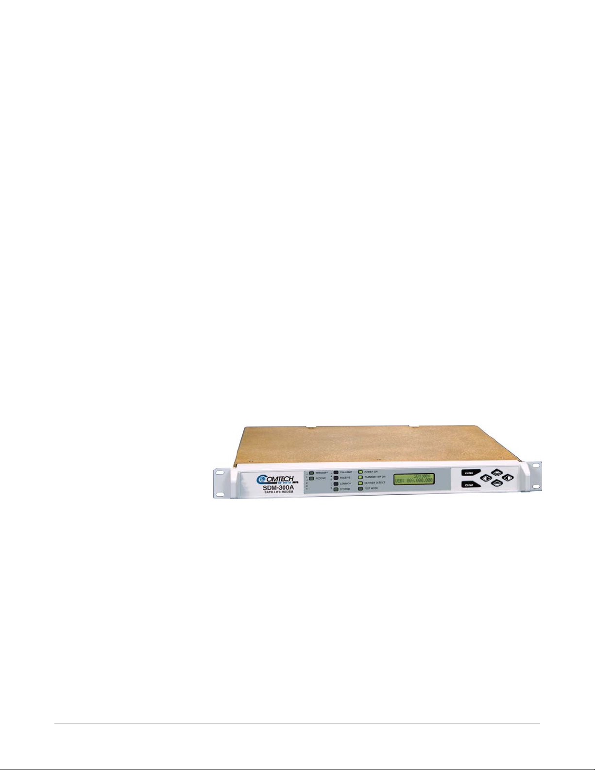
The SDM-300A is a complete, self-contained unit in a standard, one-rack unit (1 RU), 19-inch
(48 cm), rack-mountable enclosure weighing approximately 9 lbs (4 kg). The unit was
constructed using modular design and consists of from two to five Printed Circuit Boards
(PCBs), depending on the configuration. The modem consists of two major, replaceable
assemblies as follows:
• Rear panel, main PCB, and power supply
• Upper and lower enclosures (chassis) and the front panel
The front panel of the modem contains all Monitor and Control (M&C) function indicators used
for operating the modem. The modem can be operated remotely via the M&C connection on the
rear panel.
SDM-300A
Satellite Modem
Chapter 1. Introduction
1–1
Page 28
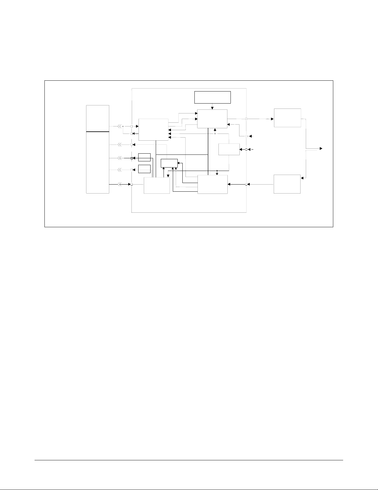
SDM-300A Satellite Modem Revision 6
Introduction MN/SDM300A.IOM
Refer to Figure 1-1for a system block diagram.
-5
2x10 REFERENCE
2x10 R EF (OPT )
DATA
I/Q
AGC
-7
ENCODER/
MODULATOR
DEMOD/
DECODER
POWER
SUPPLY
IF OUTPUT
CP 1
50 TO 18 0 MHZ
-5 TO -30 DBM
+5 TO -20 DBM OPTION
CP3 EXT REF
(OPTION)
90 TO 26 4 VAC,
47 TO 63 HZ
IF INPUT
CP2
50 TO180 MHZ
-30 TO-55 DBM
TRANSMIT
RF
EQUIPMENT
RECEIVE
RF
EQUIPMENT
ANTENNA
BOP
(Optional)
CUSTOMER
DATA I\O
AUX 1
TTL FAULTS
x
FAULT
FORM C
CONTACTS
x
ALARMS
FORM C
CONTACTS
x
REMOTE
SERIAL
INTERFACE
SDM-300A
SATELLITE
MODEM
J8
J8
x
J9
x
J7
x
J10
x
J6
INTERFACE
FAULT
RELAYS
ALARM
RELAYS
M&C
AUX
CIRCUITS
DATA
CLK
SCT
SAT CLK
1
Figure 1-1. Block Diagram
Notes:
1. The UB-530 universal breakout panel (BOP) is an option for breaking out the V.35,
G.703, RS-232, or RS-422 signals from the 50-pin data I/O connector.
2. When the modem is equipped with a 50-pin data I/O connector, the use of the BOP is
required to interface the customer data connector to the modem.
3. Contact Comtech EF Data Customer Support department for information concerning
universal breakout panels.
1–2
Page 29

SDM-300A Satellite Modem Revision 6
Introduction MN/SDM300A.IOM
1.1 Overview
The SDM-300A Satellite Modem is a high performance, full-duplex, digital-vector,
modulator/demodulator that meets the open network requirements of the INTELSAT Earth
Station Standards (IESS) -308, -309, and -310 emulation specifications for the following:
• Intermediate Data Rate (IDR)
• INTELSAT Business Services (IBS)
• Satellite Multiservice System (SMS)
Additionally, the modem is used for many closed network satellite communication systems.
1.1.1 Modem Functions
Modulator Demodulator
Performs filtered BPSK, QPSK, Offset QPSK, and 8-PSK
modulation onto a variable frequency/amplitude carrier.
Encodes the data for the appropriate decoder. Decodes the data.
Scrambles the data. Descrambles the data.
Monitors and displays the modulator status without
interrupting service.
Performs self-test. Performs self-test.
Provide send clock timing.
Performs filtered BPSK, QPSK, Offset QPSK, and 8-PSK
demodulation from carriers of variable frequencies/amplitudes.
Monitors and displays the demodulator status without interrupting
service
1.1.2 Standard Features
• Differential encoder/decoder
• Built-in scramblers/descramblers
• TX and RX frequency synthesizers
• Multi-rate FEC convolutional Viterbi and Sequential Decoder
• Fully Accessible System Topology (FAST)
• Built-in self test
• Asymmetrical loop timing
• IDR Engineering Service Circuit (ESC) channel option of 64k data or two audio
channels
• Space Link Remote Control (SLRC)
• Selectable near or far end, baseband or interface loopback with any overhead option
enabled
1–3
Page 30

SDM-300A Satellite Modem Revision 6
Introduction MN/SDM300A.IOM
1.1.3 Description of Interface Functions
An interface consists of a device having the following functions:
• Terrestrial Data Interface or a Terrestrial Voice Interface including terrestrial interface
to Engineering Service Channels (ESC).
• Multiplex various types of ESCs into the data.
• Demultiplex various types of ESCs from the data.
• Buffer the RX data.
• Monitor and display the interface status without interrupting service.
• Perform Self-Test.
1.1.4 Modes of Operation
The following modes of operation are supported:
• ASYNC Overhead Interface with AUPC (see Note 1) • SDM-100 Emulation
• CDM Compatibile • SDM-650 Emulation
• Custom (see Note 2) • SDM-6000 Emulation
• Drop & Insert (D&I) • SDM-300 Emulation
• EFD Closed Network • SDM-308 Emulation
• IDR • SDM-309 Emulation
• IBS • CDM Compatible
Notes:
1. The ASYNC/AUPC option allows an additional overhead channel to be multiplexed
and demultiplexed from the data carrier.
2. The Custom mode of operation enables the programming of the modem for emulating
most proprietary modems.
Two mechanisms are provided for uplink power control within a closed network.
• One method, which requires the optional ASYNC/AUPC interface card, is used for
control between two links to sustain sufficient transmit power to maintain a
programmed Eb/No at both ends.
• The second method is used for self-monitoring the carrier from the same uplink with the
local demodulator, requires no additional hardware, and is software-selectable. This
method is appropriate for applications such as paging networks, where the uplink is
transmitting to receive-only devices.
The modem interfaces between the channel unit or Multiplexer (MUX) and Intermediate
Frequency (IF) converter equipment operating in a 50 to 180 MHz band. An internal channel
unit, conforming to IESS-308, -309, and -310 emulation specifications, provides overhead
designated for an ESC.
1–4
Page 31

SDM-300A Satellite Modem Revision 6
Introduction MN/SDM300A.IOM
The modem is used in Single Channel Per Carrier (SCPC) applications within the following
specifications:
• Modulation type of QPSK, BPSK, 8-PSK, or Offset QPSK
• Forward Error Correction of 1/2, 3/4, 7/8, 1/1 or 2/3
• Symbol rate of 4.8 ks/s to 2.5 Ms/s
The modem can be configured to add overhead/framing to the data. Available modulation types
include:
• Bi-Phase Shift Keying (BPSK)
• Quadrature Phase Shift Keying (QPSK)
• Offset Quadrature Phase Shift Keying (OQPSK)
• 8- Phase Shift Keying (8-PSK)
1–5
Page 32

SDM-300A Satellite Modem Revision 6
Introduction MN/SDM300A.IOM
1.2 Options
Table 1-1. Options
Option Decsription & Comments
50Ω IF Impedance
-20 to +5 dBm IF output
Sequential, Viterbi,
Reed-Solomon or
Turbo Product Codec
Notes:
R-S concatenates with Viterbi or Sequential
ONLY.
For Turbo, Revision C (or later) main board is
required.
OQPSK
8-PSK, 2/3 rate, IESS-310 Requires Viterbi and Reed-Solomon Codec
8-PSK, 2/3 rate, EFD Mode Requires Viterbi Codec
8-PSK, 3/4 rate, Turbo Requires Turbo Product Codec
Asynchronous Overhead Includes automatic uplink power control (AUPC)
IBS and IDR Overhead
Drop & Insert Overhead
RS-422/RS-449 Interface
48 VDC Input Power
Single Data/Code Rate
≤ 512 kbps maximum data rate
≤ 5.0 Mbps maximum data rate
High Stability Reference
Asymmetrical Loop Timing (ASLT)
Transmit Only
-20 dB return loss 50 to 180 MHz
nd
Output 2
< 50 dBc at data rates ≥ 64 kbps
Modem can be supplied with any combination of:
Internal stability = ± 0.2 PPM, with the ability to drive out the external reference
connector
Harmonics: < 45 dBc at data rates < 64 kbps
• Sequential
• Viterbi
• Reed-Solomon
• Turbo
Receive Only
Mux Available in: 4- or 8-Channel
Flex Mux
Eurocomm Interface Requires Overhead Card
G.703 Interface with DB-15 and BNC (Closed
Network)
2 x ADPCM Voice in 64 kbps IBS Frame Requires Overhead Card
RS-530 Interface
RS-232 Interface
V.35 Interface
High Stability
IESS-315 Srambling Turbo Mode
Requires Overhead Card
Internal Clock Stability ± 2 x 10
1–6
-7
Page 33

SDM-300A Satellite Modem Revision 6
Introduction MN/SDM300A.IOM
1.2.1 Factory-Installed Options
Consult a Comtech EF Data Customer Support representative for modem options. The
following options are installed at the factory:
• Output Impedance: 75Ω (50Ω
Optional)
• High Stability Reference Oscillator
• High-power version (+5 to -20 dBm)
1.2.2 Factory- or User-Installed Options
Consult a Comtech EF Data Customer Support representative for modem options. The
following options can be factory- or user-installed:
• Turbo Product Codec (TPC)
• INTELSAT/Closed Network TX or RX Reed-Solomon
• Overhead (G.703/IBS/IDR/ASYNC/AUPC/D&I)
• MUX:
♦ 4-Channel (SYNC)
♦ 8-Channel (SYNC)
♦ 4-Channel (ASYNC)
♦ 8-Channel (ASYNC)
♦ 4-Channel (ASYNC/SYNC)
♦ 8-Channel (ASYNC/SYNC)
• Flex MUX
1–7
Page 34

SDM-300A Satellite Modem Revision 6
Introduction MN/SDM300A.IOM
1.3 Description of FAST Options
The modem has a variety of hardware options available as shown in Table 1-3. Hardware
options are available through conventional means as well as through Comtech EF Data’s FAST
system. Offset QPSK mode is available through the FAST feature. For detailed descriptions of
the FAST feature and all options, refer to Chapter 18.
Note: Comtech EF Data has included a DEMO Mode in the Utility Menu. This feature will
allow the operator to experience any of the FAST options. This feature has a 60-minute time
limit, after which, the unit will return to its previous configuration.
Table 1-2. FAST Options and Required Configurations
Hardware
Basic Platform
SDM-300A
FAST Options
FAST Options with
Reed Solomon Hardware
FAST Options with
Overhead Hardware
FAST Options with
Reed Solomon And
Overhead Hardware
8 Channel Mux
Flex Mux
Notes:
1 The basic modem is shipped with either Sequential or Viterbi decoder.
2 Requires G.703 Interface module and Overhead card.
3 Either IBS OptionOption or IDR Option includes 2xADPCM voice in 64 kbps IBS.
4 Either Simplex Reed-Solomon or Turbo Codec is installed, not both.
5 Duplex Reed-Solomon and Turbo can be installed together, however, only select one at a time.
Single
Data Rate
(up to 512 kbps)
Low Variable Data Rate
z z z z z z
(up to 4.375 Mbps)
High Variable Data Rate
Sequential Decoder
z
1
Viterbi Decoder
Asymmetrical Loop
z
1
Timing
8-PSK
Drop & Insert
Reed–Solomon Codec
z
z z z z
ASYNC/AUPC Overhead
z
2
Open Network (IDR/IBS)
z
2
z
2
z
4-Channel ASYNC,
z z
8-Channel ASYNC,
SYNC or ASYNC/SYNC
SYNC or ASYNC/SYNC
Turbo
1–8
Page 35

SDM-300A Satellite Modem Revision 6
Introduction MN/SDM300A.IOM
1.4 Compatibility
The SDM-300A is functionally compatible with many Comtech EF Data modems. When
properly configured, the unit will interoperate with the following Comtech EF Data modems:
• CDM-550/550T (Viterbi and Turbo only) • SDM-6000
• CDM-600/600L (Viterbi, Open Network,
and Turbo only)
• SDM-100/100A • SDM-308-4
• SDM-300L (L1, L2 or L3) • SDM-308-5
• SDM-650B • SDM-309
• SDM-8000
1.5 Breakout Panels
1. The UB-530 universal breakout panel (BOP) is an option for breaking out the V.35, G703,
RS-232, and RS-422 signals as well as the overhead ESC and Alarm signals.
2. When the modem is equipped with a 50-pin data I/O connector, the BOP is required to
interface with the customer data.
3. The UB-54 breakout panel (BOP) is an option for MUX only.
1.5.1 UB-300 Universal Breakout Panel
The UB-300 universal breakout panel can function as an IDR, D&I, or ASYNC/AUPC data
breakout panel in one small rack-mountable unit.
Note: The 25-pin connector at J3 on the UB-300 is not an RS-530 pinout.
For more information, refer to the Comtech EF Data UB-300 Universal Breakout Panel
Installation and Operation Manual.
1.5.2 UB-530 Breakout Panel
Alternate Part for UB-300.
The UB-530 functions ths same as UB-300, except, the UB-530 has an RS-530 25-pin Data I/O
connector at J3.
For more information, refer to the Comtech EF Data UB-530 Breakout Panel Installation and
Operation Manual.
1–9
Page 36

SDM-300A Satellite Modem Revision 6
Introduction MN/SDM300A.IOM
1.5.3 UB-54 Breakout Panel
The UB-54 breakout panel functions with the MUX option as a rack-mountable unit.
For more information, refer to the Comtech EF Data UB-54 Breakout Panel Installation and
Operation Manual.
1.6 Comtech EF Data Part Numbers
Table 1-3. Comtech EF Data Part Numbers
Options Decription of Options
Chassis CEFD F/P Duplex
KT/7999
OL/7625-1
LB/7989-1
Primary Input Power 90-264 VAC
KT/8000-1
Baseboard Configuration
Interface Board
Reed-Solomon (R-S)
Board
Duplex Reed-Solomon
Module
Turbo Board PL/9394-1
AC Power Cord Standard
75Ω, -5 dB Out
PL/6093-1
75Ω, +5 dB Out
PL/6093-2
25-Pin
PL/5727-1
37-Pin
PL/6031-1
TX R-S
PL/6284
TX/RX
PL/9658-1
CA/17725
IEC-320
CA/90025-5ft
CEFD RX Only
KT/7999
LB/7989-1
OL/7625-1
SS/300A-0020
-48 VDC
KT/8000-2
50Ω, -5 dB Out
PL/6093-3
50Ω, +5 dB Out
PL/6093-4
Overhead – 50P
PL/5305-2
PL/5309-2
8-Channel Mux
PL/5985
PL/6029-1
RX R-S
PL/6285
European/French
CA/17850
United Kingdom
CA/PWR83221
CEFD TX Only
KT/7999
LB/7989-1
OL/7625-1
SS/300A-0021
75Ω, -5 dB Out
-7
H/S 10
PL/6093-5
75Ω, +5 dB Out
H/S 10
PL/6093-6
50-Pin Interface
PL/6167-1
V.35 34-Pin
PL/6032-01
Australian
WI/865516035-AUS
-7
50Ω, -5 dB Out
-7
H/S 10
PL/6093-7
50Ω, +5 dB Out
H/S 10
PL/6093-8
Flex Mux
PL/6450-1
PL/6451-1
G.703/ASYNC
W/Overhead
PL/5305-2
PL/7838-1
-7
1–10
Page 37

SDM-300A Satellite Modem Revision 6
Introduction MN/SDM300A.IOM
Table 1-4. Data Interface Connector (J8) Matrix
Electrical Interface
Mechanical Connector Type RS-232 RS-422 V.35 G.703 Other
25-Pin D, Female X X (RS-530) X
34-pin Winchester, Female (Block) X
37-Pin D, Female X (RS-449)
50-Pin D Female Overhead X X X X
50-Pin D Female, Non-Overhead X X X Note 2
100-Pin Mini-D, Female, 8-Ch Mux X
50-Pin D, Female, Flex Mux Only X
15-Pin D, Female BNC,Female
(SD& RD)
Notes:
1. 50-Pin Overhead Board (PL/5305-2) required for IBS, IDR, D&I, and AUPC/ASYNC.
2. The 50-Pin D are used with (SMS-7000) Redundancy Switch and Breakout Panels.
X
Notes 1,2
Table 1-5. SDM-300A Software Selection Table
Part Number Description
SS/300A-0001 SDM300A, Software Selection for Single Data Rate
SS/300A-0002 SDM300A, Software Selection for Variable Data Rate 2.4 to 512 kbps
SS/300A-0003 SDM300A, Software Selection for Variable Data Rate 2.4 to 5000 kbps
SS/300A-0004 SDM300A, Software Selection for Viterbi Decoder
SS/300A-0005 SDM300A, Software Selection for Sequential Decoder
SS/300A-0006 SDM300A, Software Selection for Asymmetrical Loop Timing
SS/300A-0007 SDM300A, Software Selection for 8-PSK Modulation
SS/300A-0008 SDM300A, Software Selection for G.703 Operation
SS/300A-0009 SDM300A, Software Selection for IDR Operation
SS/300A-00010 SDM300A, Software Selection for IBS Operation
SS/300A-00011 SDM300A, Software Selection for AUPC with ASYNC Operation
SS/300A-00012 SDM300A, Software Selection for Drop & Insert Operation
SS/300A-00013 Reserved
SS/300A-00014 SDM300A, Software Selection for 4 Channel MUX Card, SYNC
SS/300A-00015 SDM300A, Software Selection for 8 Channel MUX Card, SYNC
SS/300A-00016 SDM300A, Software Selection for 4 Channel MUX Card, ASYNC
SS/300A-00017 SDM300A, Software Selection for 8 Channel MUX Card, ASYNC
SS/300A-00018 SDM300A, Software Selection for Reed-Solomon, RX Mode
SS/300A-00019 SDM300A, Software Selection for Reed-Solomon, TX Mode
SS/300A-00020 SDM300A, Software Selection for Receive Only Mode
SS/300A-00021 SDM300A, Software Selection for Transmit Mode Only
SS/300A-00022 SDM300A, Software Selection for Offset QPSK Modulation
SS/300A-00023 Reserved
SS/300A-00024 SDM300A, Software Selection for AUPC (No ASYNC) Operation
1–11
Page 38

SDM-300A Satellite Modem Revision 6
Introduction MN/SDM300A.IOM
Table 1-6. SDM-300A Spares/Accessories
Part No. Description Comments
KT/8000-1 Chassis – AC Power Supply
KT/8000-2 Chassis – DC Power Supply
PS/AC65W01P02 AC Power Supply
PS/DC-DC5V65W DC Power Supply
PL/6093-1
PL/6093-2
PL/6093-3
PL/6093-4
PL/6093-5
PL/6093-6
PL/6093-7
PL/6093-8
PL/6284 Intelsat Reed-Solomon Board – TX
PL/6285 Intelsat Reed-Solomon Board – RX
PL/9394-1 TX/RX Turbo Codec Board
PL/9658-1 Duplex Reed-Solomon Can be installed with
KT/9672-1 TX/RX Turbo Codec Upgrade Kit
Interfaces
PL/5305-2
KT/9521-1
PL/5727-1 25-Pin D Type Interface Board
PL6031-1 37-Pin D Type Interface Board
PL/6167-1 50-Pin D Type Interface (No Overhead)
PL/6032-1 34-Pin “Winchester” Block V.35 Interface Board
PL/7838-1 G.703; ASYNC Personality Board Requires Overhead
PL/6450 Flex MUX Board
PL/6451 Flex MUX Board Personality Board
PL/5985 8-Channel MUX Board
PL/6029-1 8 Channel MUX Personality Board
CIM-25: IP enabled M&C Interface Contact CEFD
- 5 dB output, 75Ω
+ 5 dB output, 75Ω
- 5 dB output, 50Ω
+ 5 dB output, 50Ω
- 5 dB output, 75Ω, High Stability 10
+ 5 dB output, 75Ω, High Stability 10
- 5 dB output, 50Ω, High Stability 10
+ 5 dB output, 50Ω, High Stability 10
Note: Turbo is only compatible with PL/9658-1 ReedSolmon Duplex Mode.
Note: Turbo is not available with TX/RX Reed-Solomon.
50-Pin Overhead/Interface (AUPC with ASYNC)
FAST upgrade to activate: G.703; IDR; IBS; ASYNC;
D&I
Note: Overhead Board is not available with Flex MUX.
-7
-7
-7
-7
Reed-Solomon is not
available with Turbo.
Reed-Solomon is not
available with Turbo.
Requires Main Board
PL/6093-X, Rev. C
Turbo.
Requires Main Board
PL/6093-X, Rev. C
Hardware KT/5305-2
Requires FAST
upgrade
Board
Customer Support
1–12
Page 39

SDM-300A Satellite Modem Revision 6
Introduction MN/SDM300A.IOM
1.7 New in this Release
This manual was reformatted in accordance with Comtech EF Data procedures.
General – Manual completely revised. Only technical changes are provided in this paragraph.
Incorporate FW/6535AJ1, Version No. 7.1.8
Updated Comtech EF Data Part Numbers
Added Turbo Codec installation.
Added Duplex Reed-Solomon Codec installation.
Added Flash Upgrading.
Added Remove and Replace Power Supply.
Added Remove and Replace the fan Assembly.
1–13
Page 40

SDM-300A Satellite Modem Revision 6
Introduction MN/SDM300A.IOM
This page is intentionally left blank.
1–14
Page 41

Chapter 2. Functional Description
2.1 Description of Monitor and Control (M&C)
The M&C monitors the modem and provides configuration updates to other modems within the
modem when necessary.The modem configuration parameters are maintained in battery-backed
RAM, which provides total recovery after power-down situation.The M&C functions include
extensive fault and status reporting.All modem functions are accessible through a local front
panel interface and a remote communications interface.
A block diagram of the M&C is shown in Figure 2-1.
2.1.1 Theory of Operation
The M&C card is composed of the following subsections:
• Microcontroller with Universal Asynchronous Receiver/Transmitter (UART)
• Digital-to-Analog Converter (DAC)
• Read Only Memory (ROM)
• Analog-to-Digital Converter (ADC)
• Read Access Memory (RAM)
• Universal ASYNC
• User Interface
• Fault and Alarm Relays
2–1
Page 42

SDM-300A Satellite Modem Revision 6
Functional Description MN/SDM300A.IOM
FAULT
MODEM
AND ALARM
RELAYS
11 M Hz
CLOCK
DAC
ADC
2
IC BUS
CONTROLLER
EIA-232
OR
EIA-485
ROM
(M&C,
BULK,
BOOT)
MICRO-
RAM AND
REAL
TIME
CLOCK
9-PIN
REMOTE
Figure 2-1. M&C Block Diagram
2–2
Page 43

SDM-300A Satellite Modem Revision 6
Functional Description MN/SDM300A.IOM
The heart of the M&C card is the Dallas 80C310 microcontroller operating at 11 MHz. This
microcontroller contains 256 kbytes of internal RAM. The ROM at U8 is 29F040 (512 kbytes).
• ROM access times must be ≥ 150 ns. The RAM can be 8 or 32 kbytes in size.
• This RAM chip is internally battery-backed and contains a real time clock used by the
M&C.
The non-volatile RAM on the M&C module allows the module to retain configuration
information without prime power for 1 year (approximately). If the modem is powered down,
the following sequence is carried out by the M&C microcontroller.
1. When power is applied to the M&C, the microcontroller checks the non-volatile
memory to see if valid data has been retained. If valid data has been retained, the
modem is reconfigured to the parameters maintained by the RAM.
2. If the non-volatile memory fails the valid data test, a default configuration from ROM is
loaded into the system.
The UART supports serial ASYNC communications channels (remote port) with a maximum
data rate of 19200 bps. The UART is a built-in peripheral of the microcontroller. The
communications type can be RS-232, RS-485 (2-wire), RS-485 (4-wire), and software
selectable.
The DAC supplies a voltage that controls the contrast of the display. The ADC monitors all the
voltages from the power supply. The DAC and ADC are mapped to the microcontroller with an
Integrated Circuit (IC) bus.
The user interface includes the following parts:
• Front panel
• Status LEDs
• Keyboard
• Sounder (beeper)
All functions are memory-mapped to the microcontroller.
2–3
Page 44

SDM-300A Satellite Modem Revision 6
Functional Description MN/SDM300A.IOM
2.1.2 Remote Baud Rate
The remote communications baud rate and parity are programmed by the front panel control in
the Utility: System menu (refer to Chapter 5). The programmed baud rate and parity are
maintained indefinitely in RAM on the M&C module. The parity bps can be set to EVEN or
ODD. The available baud rate are listed below:
• 110
• 150
• 300
• 600
• 1200
• 2400
• 4800
• 9600
• 19200
2.1.3 Remote Address
To communicate with the established remote communications protocol, configure each modem
for one address between 1 and 255. Each modem on a common remote communications link
(RS-485) must have a distinct address. Use the front panel control in the Utility: System menu
(Chapter 5) to program the address.
An RS-485/RS-232 communications link remotely controls and monitors all modem functions.
Use the 2- or 4-wire, half-duplex RS-485 interface to connect between two or more modems
and switches on a common communications link. Use the RS-232 interface to communicate
with a single modem.
Note: Address 0 is reserved as a global address which simultaneously addresses all devices on a
given communications link.
2–4
Page 45

SDM-300A Satellite Modem Revision 6
O
UTPU
Functional Description MN/SDM300A.IOM
2.2 Description of the Modulator
The modulator provides PSK modulated carriers within the 50 to 180 MHz range. The types of
modulation that encode the transmitted baseband data from the interface PCB are:
• BPSK
• QPSK
• Offset QPSK
• 8-PSK
Refer to Section 2.2.2 for a description of each modulation type.
A block diagram of the modulator is shown in Figure 2-2.
DATA
CLK
INTERFACE
SCT
REFERENCE
OPTIONAL
FRAMING UNIT
IBS/IDR, ASYNC/AUPC
DROP & INSERT
SCT
PLL
OPTIONAL
LO
Figure 2-2. Modulator Block Diagram
OPTIONAL
REED-SOLOMON
ENCODER
BPF
BPF
MUX
CONVOLUTIONAL
ENCODER
DIGITAL
SIGNAL
PROCESSING
POWER LEVEL
CONTROL
MONITOR
&
CONTROL
LPF
RF LOOPBACK
T
RF
OUTPUT
2–5
Page 46

SDM-300A Satellite Modem Revision 6
Functional Description MN/SDM300A.IOM
2.2.1 Theory of Operation
The modulator is composed of eight basic subsections. These subsections are divided into the
baseband processing section and the RF section of the modulator. The modulator controls all
programmable functions on this module. Fault information from the modulator is sent to the
M&C.
The major modulator subsections are:
• Scrambler/Differential Encoder
• Convolutional Encoder
• Programmable Vector Rotation
• I/Q Nyquist Filters
• Modulator
• RF Synthesizer
• Output Amplifier
• Output Level Control
If the modem is so equipped, the optional overhead or Reed-Solomon PCB first processes the
data. The data is then sent to the scrambler for energy dispersal, and then to the differential
encoder. The differential encoder is a 2-bit encoder, which allows for resolution of two of the
four ambiguity states of the QPSK or Offset QPSK demodulator.
The data is sent to the convolutional encoder for encoding the baseband data. The code rates
1/2, 3/4, 7/8, and 2/3 are based on the symbol rate range of 2.4 kbps to 2.5 Mbps.
• For Viterbi codes, the convolutional encoder encodes the data at 1/2 rate. If the selected
code rate is 3/4, then 2 of every 6 symbols are punctured. For 3 bits in, there are 4 symbols
out.
• For Sequential codes, the convolutional encoder generates the parity bits from the input data
stream, which allows for error correction at the far end of the link. The rate of the encoder
may be 1/2, 3/4, 7/8, and 2/3.
For example, the 7/8 rate puts out 8 symbols for every 7 bits in. In QPSK (or Offset
QPSK) mode, the data is split into two separate data streams to drive the I and Q channels
of the modulator. Refer to Section 2.2.2 for the theory of modulation types.
After the convolutional encoder, the data is sent to a programmable vector rotation circuit. This
feature provides the user with data communications compatibility for spectrum reversal of the I
and Q channels before and after satellite transmission.
The I and Q channel data then pass through a set of variable rate digital Nyquist filters.
2–6
Page 47

SDM-300A Satellite Modem Revision 6
Functional Description MN/SDM300A.IOM
Direct Digital Modulation follows the two identical digital Nyquist filters. Symbol rates up to
2.5 Mbps can be achieved automatically.
The modulated carrier is applied to the RF section for conversion to the correct output
frequency. The spectral shape will be identical to that of the input data streams, but
double-sided about the carrier frequency.
The RF synthesizer provides the proper frequencies to convert the modulator IF to the desired
output frequency in the 50 to 180 MHz range. The synthesizer has a single loop, and
incorporates a Direct Digital Synthesis (DDS) chip to accommodate 1 Hz steps over a range of
130 MHz. The RF section has a frequency stability of
± 1 x 10
-5
. An optional 2 x 10⁻⁷
Temperature Compensated Crystal Oscillator (TCXO) can be installed.
The signal is sent to the output amplifier. The amplifier takes the low level signal from the
modulator section and amplifies the signal to the proper level for output from the module. The
amplifier circuitry provides programmable control of the output level over a range of -5 to -30
dB, in 0.1 dB steps. The amplifier has power leveling of
± 0.5 dB to maintain the stability of the
output level over time and temperature. The +5 dB output option is capable of outputting +5 to 20 dBm.
2.2.2 Theory of Modulation Types
The modulation types for the modem include BPSK, QPSK, Offset QPSK, or 8-PSK.
The PSK data transmission encoding method uses the phase modulation technique. This method
varies the phase angle of the carrier wave to represent a different bit value for the receiver. The
higher levels of modulation are required for an operating range that has a limited bandwidth.
The order of modulation is represented by mPSK, where “m” relates to the number of discrete
phase angles. Refer to the following list for a brief description of the modulation types.
BPSK
QPSK
8PSK
Note: The code rate determines the number of symbols per bit.
2 discrete phase angles represent the 2 possible states of a symbol.
4 discrete phase angles represent the 4 possible states of a symbol.
8 discrete phase angles represent the 8 possible states of a symbol.
2–7
Page 48

SDM-300A Satellite Modem Revision 6
Functional Description MN/SDM300A.IOM
2.3 Description of the Demodulator
A block diagram of the demodulator is shown in Figure 2-3.
The demodulator converts PSK modulated carriers within the 50 to 180 MHz range to a
demodulated baseband data stream. The converted modulation types are BPSK, Offset QPSK,
QPSK, and 8-PSK (refer to Section 2.2.2 for a description of modulation types). The
demodulator then performs FEC on the data stream using Viterbi or Sequential decoding
algorithms.
LOOPBACK
RF INPUT
SWITCH
RF INPUT
50 TO 180 MHz
REF
VCXO
OC XO
OPT
HIGH
STABILITY
EXT REFERENCE
AGC
REF
PLL
LPF BPF
LO #1
REFERENCE
SEQUENTIAL
DECODER
OPTIONAL
REED-SOLOMON
OPTIONAL
OVERHEAD DEFRAMING
IBS/IDR, ASYNC/AUPC
DROP & INSERT
VITERBI
DECODER
CODEC
LO #2
OPTIONAL
TURBO
CODEC
MUX
CONVERTER
PROCESSING
DOPPLER/
PLESIOCHRONOUS
BUFFER
Figure 2-3. Demodulator Block Diagram
BPF
ATOD
DIGITAL
SIGNAL
DIGITAL
CLOCK
RECOVERY-
LOOP
INTERFACE
2–8
Page 49

SDM-300A Satellite Modem Revision 6
Functional Description MN/SDM300A.IOM
2.3.1 Theory of Operation
The demodulator functions as an advanced, digital, coherent-phase-lock receiver and decoder.
Demodulator faults are also reported to the front panel. The demodulator consists of the
following basic subsections.
• Digital Costas Loop
• RF Section
• Automatic Gain Control
• Analog-to-Digital (A/D) Converter
• Soft Decision Mapping
• Programmable Vector Rotation
• Digital Nyquist Filters
• FEC Decoder
• Digital Clock Recovery Loop
• Decoder
The modulated IF signal at 50 to 180 MHz enters the RF module for conversion to an IF
frequency. The IF is then sampled by an A to D converter and digitally demodulated. The I and
Q data is then sent to the digital Nyquist filters, resulting in a filtered, digital representation of
the received signal. The digital data is then sent to four separate circuits:
• Automatic Gain Control
• Carrier Recovery (Costas) Loop
• Clock Recovery Loop
• Soft Decision Mapping
The AGC provides a gain feedback signal to the RF section. This closed loop control ensures
that the digital representation of the I and Q channels is optimized for the Costas and Clock
loops, as well as the soft-decision mapping circuitry.
When the active decoder determines that the modem is locked, the M&C stops the sweep and
begins the de-stress process. This involves fine-tuning the DDS based on the phase error in the
Costas loop. The de-stress process continues as long as the modem is locked. If the carrier is
interrupted, the M&C resumes the sweep process.
The digital Costas loop, in conjunction with a Direct Digital Synthesizer (DDS), performs the
carrier recovery function. The Costas loop consists of a Costas phase detector, loop filter, and
DDS, all implemented digitally. The DDS performs the function of a Voltage-Controlled
Oscillator (VCO) in an analog implementation, but can be easily programmed to the desired
center frequency via the M&C. The output of the DDS is sent to the RF module and provides
the reference to which the local oscillator is locked. The M&C sweeps the local oscillator (via
DDS programming) through the user-specified sweep range.
The digital clock loop, in conjunction with another DDS, performs the clock recovery function.
The clock loop consists of a phase detector, loop filter, and DDS, all implemented digitally. The
DDS performs the function of a VCO in an analog implementation. The recovered data and
symbol clocks are then used throughout the demodulator.
2–9
Page 50

SDM-300A Satellite Modem Revision 6
Functional Description MN/SDM300A.IOM
The soft decision mapper converts the digital I and Q data to 3-bit soft decision values. These
values are then fed to the programmable vector rotation circuit, providing compatibility with
spectrum reversal of the I and Q channels.
The output of the vector rotation circuit is then sent to the Viterbi decoder and optional
Sequential decoder. The output is then sent to the optional Reed-Solomon or Overhead PCB.
2.4 Description of the Decoder
The SDM-300A can be configured in any of the following configurations:
• Basic SDM-300A (Sequential or Viterbi Decoder)
• FAST options (Sequential or Viterbi Decoder)
• FAST options with Reed-Solomon hardware (Sequential or Viterbi Decoder)
• FAST options with Overhead hardware (Sequential or Viterbi Decoder)
• FAST options with Reed-Solomon and Overhead hardware
(Sequential or Viterbi Decoder)
2–10
Page 51

SDM-300A Satellite Modem Revision 6
Functional Description MN/SDM300A.IOM
2.5 Description of the Interface
The terrestrial interface functions include:
• MUX various types of ESC into the data
• Buffering the receive data
• DEMUX various types of ESC from the data
• Monitoring and displaying the interface status without interruption of service
The interface block diagram is shown in Figure 2-4.
The terrestrial interfaces for the modem are defined by data communication standards RS530/RS-449, RS-232, or V.35. The interface receivers and drivers for these standards, as well as
the handshake signals for all formats, are selectable through the front panel menus.
Overhead can be added to the terrestrial data for other modes of operation. The format of the
overhead data is dependent on the mode of operation and requires one of the following options
used with the interface PCB:
• ASYNC/AUPC
• D&I
• IBS
• IDR
2–11
Page 52

SDM-300A Satellite Modem Revision 6
Functional Description MN/SDM300A.IOM
INTERFACE
LOOPBACK
TX
OVERHEAD
TX T ERR
DATA
BASEBAND
LOOPBACK
RECEIVERS
LINE
RECEIVERS
OVERHEAD
P
ROCE SSORS
SCT
EXT
TX
CLOCK
MUX
DROP/INSERT
TX
OVERHEAD
MUX
RS CODEC
TXSAT
DATA
RXTER R
DATA
OVERHEAD
RX
BACKWARD
ALARMS
MODEM
(FORM C)
MODEM
(TTL)
FAULTS
FAU LT S
RXCLK
SCT
EXT
TXCLK
HI STAB
LINE
DRIVERS
PLESIOCHRONOUS
BUFFER
OVERHEAD
RX
CLOCK
MUX
LINE
DRIVERS
BWA
FORM
RELAYS
FLT
FORM
RELAYS
C
C
PROCESSORS
RELAY
DRIVERS
RELAY
DRIVERS
TTL
DRI VERS
Figure 2-4. Interface Block Diagram
RX
OVERHEAD
DEMUX
MICR O-
CONTROLLER
RXSAT
DATA
2–12
Page 53

SDM-300A Satellite Modem Revision 6
Functional Description MN/SDM300A.IOM
2.5.1 Available Interfaces
The following data interfaces are available for the SDM-300A:
• EIA-232 (25-Pin D Sub)
• EIA-422 (37-Pin D Sub)
• EIA-530 (25-pin D Sub)
• G.703 (BNC and DB15)
• V.35 (34-Pin Winchester)
2.5.2 Plesiochronous/Doppler/Buffer
Data from the DEMUX section is fed into a buffer. This buffer size is user-selectable in bit
increments that correspond to the length of an IESS-308 satellite superframe. The increments
range from 1 to 32 ms. Refer to the interface specifications for a list of valid entries for each of
the selected formats. The buffer automatically centers on resumption of service, either from the
front panel or remotely. The startup buffer will overfill when centering to match the satellite
frame to the terrestrial frame with a maximum slide of 0.5 ms.
The fill status is available as a monitor and is accurate to 1%. Overflows or underflows are
stored in the stored fault section of the M&C status registers, along with the date and time of the
incident (which are provided by the modem internal clock). These are stored in battery-backed
RAM.
A normal selection is to have the data clocked out of the buffer by an external clock. This
procedure removes the Doppler from the receive satellite data.
The operator may select from four other clock sources as a backup:
• Insert clock (D&I mode only)
• RX satellite
• Internal clock source
• TX terrestrial
Problems occurring on any of the selected clocks will cause the modem to substitute the satellite
clock and a fault will be signaled.
2–13
Page 54

SDM-300A Satellite Modem Revision 6
Functional Description MN/SDM300A.IOM
2.5.3 Closed Network
Typically, the closed network operation does not add overhead to the terrestrial data. The closed
network operation is not dictated by a specification. The terrestrial data and clock are passed
through the baseband loopback relay and are translated from the selected baseband format to
TTL. The data is re-synchronized by the clock and the data stream is then output to the
modulator through the interface loopback device.
The receive data from the demodulator/decoder is input to the buffer. User data from the
DEMUX section may be optionally input to the buffer.
The front panel interface provides four clock selections clocking the data out of the buffer:
• Internal Clock (SCT)
• RX Recovered Clock (RXCLK)
• External Clock (EXT)
• TX Clock Dejittered (TXCLK)
If either RXCLK, SCT, or EXT is selected and then fails, the interface will automatically switch
to RX Sat CLK as the source. The receive data and selected clock are translated to the levels of
the selected baseband interface and output through the baseband loopback relay.
2.5.4 Open Network
The modem is a high-performance, full-duplex, digital-vector modulator/demodulator. The
modem meets the open network requirements of the INTELSAT IESS-308 and -309
specifications for IDR, IBS, and EUTELSAT SMS.
2–14
Page 55

SDM-300A Satellite Modem Revision 6
Functional Description MN/SDM300A.IOM
2.6 Backward Alarm Theory and Connections
Four sets of TX and RX backward alarms are available to implement the structure defined in
IESS-308. Backward alarms are sent to the distant side of an IDR link to signal that trouble has
occurred at the receive side (which may have resulted from an improper transmission).
INTELSAT specifies that any major failure of the downlink chain will generate a backward alarm.
Implementation is straightforward in a simple, single-destination link. The modem has a
demodulator fault relay which de-energizes in the event of a receive fault. For this relay to be
connected to the appropriate backward alarm input, the Fault menu for this signal includes the
appropriate overhead framing faults.
This signal also includes faults in the downlink chain, since major problems with the antenna, Low
Noise Amplifier (LNA), down converter, and other components will cause an interruption in
service and fault the modem.
The outputs of the demodulator fault relay are available as follows:
• Pins DF-C and DF-NO on the 50-pin D IDR interface connector (J8)
• 9-pin D modem fault connector (J7)
The relay contacts are named for the faulted state. If a receive fault does not occur, DF-C is
connected to DF-NO. The preferred method of using a backward alarm in a single-destination
system is to connect the signals at the IDR data interface (at the modem in a non-redundant
system, or at the protection switch, if used).
Signal Pin #
GND DB50-2
BWI1 DB50-12
BWI2 DB50-13
BWI3 DB50-14
BWI4 DB50-15
DF-C DB50-16
DF-NO DB50-50
This method signals faults on all four alarm channels, and is compatible with a redundancy system.
The method assumes that the same modem handles traffic in both directions in each
single-destination link.
To handle more complicated systems, connect the appropriate outputs of the Demod fault relay to
the appropriate backward alarm inputs. In a multi-destination system, connect the relay to the
particular backward alarm assigned to that link. Refer to IESS-308 for further clarification.
2–15
Page 56

SDM-300A Satellite Modem Revision 6
Functional Description MN/SDM300A.IOM
A backward alarm being received on a particular link is detected by one of the two following
methods:
• The backward alarm output drives a FORM C relay with all three contacts available on
the data connector.
• The status of all transmit and receive backward alarms may be read through the RS-232
or RS-485 remote interface connector that is integrating a modem or switch into a
computer network.
In addition to the four backward alarms for IDR and two backward alarms (primary and
secondary) for IBS, all modes support the following faults:
• MOD (modulator equipment)
• DEM (demodulator equipment)
• CEQ (common equipment)
Each fault is indicated by a FORM C relay contact and an open collector output.
2–16
Page 57

Chapter 3. Installation/
Upgrades
The equipment contains parts and assemblies sensitive to damage by
Electrostatic Discharge (ESD). Use ESD precautionary procedures when
CAUTION
touching, removing, or inserting PCBs.
3.1 Unpacking
The modem and manual are packaged in pre-formed, reusable, cardboard cartons containing
foam spacing for maximum shipping protection.
Do not use any cutting tool that will extend more than 1 inch into the
container. This can cause damage to the modem.
CAUTION
Unpack the modem as follows:
1. Cut the tape at the top of the carton indicated by OPEN THIS END.
2. Remove the cardboard/foam space covering the modem.
3. Remove the modem, manual, and power cord from the carton.
4. Save the packing material for storage or reshipment purposes.
5. Inspect the equipment for any possible damage incurred during shipment.
6. Check the equipment against the packing list to ensure the shipment is correct.
7. Refer to Section 3.2 for installation instructions.
3–1
Page 58

SDM-300A Satellite Modem Revision 6
Installation/Upgrades MN/SDM300A.IOM
3.2 Installation
The modem arrives fully assembled from the factory. After unpacking the modem, install the
modem as follows:
Modem Installation (Optional):
Refer to Figure 3-1. Use the following mounting kit, KT/6228-1.
QTY Part Number Description
2 FP/6138-1 Bracket, Rear Support
4 HW/10-32x1/2RK Bolt #10 Rack
2 HW/10-32x1/4 SHC Screw, Socket 10-32 x 1/4 inch
Tools Required:
Screw Driver
5/32 - inch
Phillips
SAE Allen Wrench
1. If required, install the mounting bracket (KT/6228-1) in equipment rack (Figure 3-1).
Install and tighten the bracket bolts.
2. Loosen the screw with flat washer located on the left side of modem chassis. Mount the
modem chassis into the equipment rack and slide the screw with flat washer through the
slot of the mounting bracket. Tighten the screw sufficiently to allow the modem chassis
to slide in the bracket.
3. Connect the cables to the proper locations on the rear panel.
3–2
Page 59

SDM-300A Satellite Modem Revision 6
Installation/Upgrades MN/SDM300A.IOM
Figure 3-1. Installation of the Optional Mounting Bracket, KT/6228-1
3–3
Page 60

SDM-300A Satellite Modem Revision 6
Installation/Upgrades MN/SDM300A.IOM
3.3 Software and Hardware Installation/Upgrades
3.3.1 Overhead Interface PCB Installation
The overhead interface PCB may be installed at the factory or in the field. The overhead
interface PCB is required to access certain options and functionality of the modem. Observe the
following:
• If the overhead interface PCB is installed at the factory, then the 50-pin interface relay
card will be pre-installed.
• If the overhead interface PCB is installed in the field, then one of four connector/card
combinations will have been shipped with the overhead interface PCB.
This equipment contains parts and assemblies sensitive to damage by ESD.
Use ESD precautionary procedures when touching, removing, or inserting
CAUTION
The following tool is required to install the overhead interface PCB:
Use the following information to install the overhead interface PCB as a daughter card on the
main PCB. Refer to Figure 3-2 for the installation location of the overhead interface daughter
card.
CAUTION
PCBs.
Description Application
Phillips Screwdriver
To remove and replace cross-point screws.
Turn the power off before installation. High current VDC is present. Failure
to do so could result in damage to the modem components.
1. Turn off the modem and unplug the power supply.
2. Remove the rear panel retaining screws. Using the finger pulls, slide the main modem
assembly out from the rear of the modem chassis.
3. Install the overhead interface PCB, face down, onto the main PCB by mating the male
header connectors with the female header connectors in the position shown in
Figure 3-2.
4. Align the overhead interface PCB standoffs with the main PCB mounting holes. Install
the four mounting screws and washers.
3–4
Page 61

SDM-300A Satellite Modem Revision 6
Installation/Upgrades MN/SDM300A.IOM
The mounting hardware must be installed to provide proper
grounding between the overhead interface PCB and the main PCB.
CAUTION
5. After completing the installation procedure, turn on the modem. Select the desired
modem option to use the overhead card.
Figure 3-2. Overhead Interface PCB Installation
3–5
Page 62

SDM-300A Satellite Modem Revision 6
Installation/Upgrades MN/SDM300A.IOM
3.3.2 Hardware Upgrades
3.4 Reed-Solomon PCB
3.4.1 Unpacking
This equipment contains parts and assemblies sensitive to damage by ESD.
Use ESD precautionary procedures when touching, removing, or inserting
CAUTION
PCBs.
1. Remove the Reed-Solomon PCB and mounting hardware from the cardboard
caddypack and anti-static material.
2. Check the packing list to ensure the shipment is complete.
3. Inspect the Reed-Solomon PCB for any shipping damage.
3.4.2 Installation
The following tool is required to install the overhead interface PCB:
Description Application
Phillips Screwdriver
Use the following information to install the Reed-Solomon Codec PCB as a daughter card on
the main PCB.
Refer Figure 3-3 for installation location of the Reed-Solomon daughter card.
Turn the power off before installation. High current VDC is present. Failure
to do so could result in damage to modem components.
CAUTION
1. Turn off the modem and unplug the power supply.
2. Remove the rear panel retaining screws. Using the finger pulls, slide the main modem
assembly out from the rear of the modem chassis.
3. Install the Reed-Solomon PCB to the main PCB by mating the male SIMM connectors
with the female SIMM connectors in the position shown in Figure 3-3.
To remove and replace cross-point screws.
3–6
Page 63

SDM-300A Satellite Modem Revision 6
Installation/Upgrades MN/SDM300A.IOM
4. After completing the above installation procedure, turn on the modem. If the
Reed-Solomon PCB was installed properly, the Utility: Modem Type menu will
display: “
03
Card #2 Type Reed Solomon” or “Card #3 Type Reed Solomon
” if both boards were installed.
Reed-Solomon Cards
(TX, RX, or Duplex in Either Slot)
Figure 3-3. Reed-Solomon Codec Installation
3–7
Page 64

SDM-300A Satellite Modem Revision 6
Installation/Upgrades MN/SDM300A.IOM
3.5 Turbo Codec Installation
The Turbo Card is installed in the same slots as the Reed-Solomon PCBs. While the ReedSolomon uses two cards (TX and RX), the Turbo Codec uses only a single card.
Upgrading requires installation of the Turbo Codec module, installation of
new M&C firmware, and installation of new Bulk firmware.
CAUTION
Seven Turbo code rates/modulations are supported:
• BPSK 5/16
• BPSK 21/44
• QPSK 3/4
• Offset QPSK 3/4 (requires Offset QPSK optioned modem)
• 8-PSK 3/4 (requires 8-PSK optioned modem)
• QPSK 1/2
• Offset QPSK 1/2 (requires Offset QPSK optioned modem)
3.5.1 Unpacking
This equipment contains parts and assemblies sensitive to damage by ESD.
Use ESD precautionary procedures when touching, removing, or inserting
CAUTION
PCBs.
1. Remove the Turbo Upgrade Kit that includes the following items:
• PL/9394-1 (Turbo Codec Module)
• FW/6535-1V or later version (M&C firmware)
• FW/6094W or later version (Bulk firmware)
• Installation instructions.
2. Check the packing list to ensure the shipment is complete.
3. Inspect the Turbo Codec card for any shipping damage.
3–8
Page 65

SDM-300A Satellite Modem Revision 6
Installation/Upgrades MN/SDM300A.IOM
3.5.2 Installation
The following tool is required to install the Turbo Codec card:
Description Application
Phillips Screwdriver
PLCC, Type IC Puller To firmware IC’s from the Main PCB.
SDM-300A Satellite Modem shall have Revision C (or later) Main board for Turbo upgrade.
There are two ways to determine the revision status:
Method 1: Provide the Serial Number of the modem to Comtech EF Data for verification
of the revision status.
Method 2: If the first two digits of the modem Serial Number begin with 99, 00, or 01,
corresponding to the year of the manufacture, then the modem Main board is
Revision C.
a. If the Serial Number starts with 98 then it is either Revision B or
Revision C and it is necessary to check with Comtech EF Data
Customer Support department.
b. Serial Numbers beginning with 97 or subsequent are not eligible for
upgrade.
To remove and replace cross-point screws.
Install the Turbo Codec Card on the Main PCB:
Refer Figure 3-4 for installation location of the Turbo Codec card.
Turn the power off before installation. High current VDC is present. Failure
to do so could result in damage to modem components.
CAUTION
1. Turn off the modem and unplug the power supply.
2. Remove the rear panel retaining screws. Using the finger pulls, slide the main modem
assembly out from the rear of the modem chassis.
3. If required: Card #1 Overhead Board Removal – Remove the four rear panel screws
around the 50-pin I/O switch module. Unplug the I/O module, and then remove the
seven mounting screws around the 50-pin I/O switch module. Unplug the I/O module,
then remove the seven mounting screws holding the Overhead board and carefully lift
the board out.
4. If required: Reed-Solomon Removal – Remove the Reed-Solomon boards from the
SIMM sockets by pushing the spring clips outward while the rocking the board
vertically, then lift the board out.
5. Turbo Codec Installation – Align the Turbo board with either of the SIMM sockets
while holding it vertically with components toward the Rear panel. Seat the connector
into the socket and tilt the board toward the Front Panel until the spring clips lock the
board into place.
6. Replace the top cover and reinstalled the two side screws.
7. Turn on the AC power. Modem will reinitialize.
3–9
Page 66

SDM-300A Satellite Modem Revision 6
Installation/Upgrades MN/SDM300A.IOM
Notes:
1. In this configuration, the Modem allows only Data Rates and Formats valid for
Turbo.
2. Open Network modem types cannot be selected.
Turbo Codec Installed
Figure 3-4. Turbo Codec Installation
3–10
Page 67

SDM-300A Satellite Modem Revision 6
Installation/Upgrades MN/SDM300A.IOM
Note: If replacement Firmware IC’s were sent with the Turbo Codec, perform the IC
replacement procedures.
Firmware Installation:
1. Remove existing firmware, U86 and U74 (Figure 3-5) with the PLCC type IC puller (if
puller is not available, use an ice-pick type tool to alternately and carefully pry upward at
opposite corners of the IC.
U74 U86
TURBO CODEC
INSTALLED
Figure 3-5. Firmware Location
2. Install the replacement firmware, noting that the DOT mark should be oriented toward the
beveled corner of the socket before pushing the IC into the socket. U86 is located next to
3–11
Page 68

SDM-300A Satellite Modem Revision 6
Installation/Upgrades MN/SDM300A.IOM
the lithium battery NV-RAM (large Black or Yellow IC, U95). U74 is located in the center
socket position.
3. If required, reinstalled the Overhead card and secure with seven mounting screws then
replug the I/O Module into the rear panel location. Reinstall the four mounting screws.
4. Reposition the top cover so forward edge mates under the front Panel lip. While holding in
place, reinstall the two slide screws.
5. Turn on the AC power to the modem. Modem shall re-initialize.
Turbo Setup
1. Press the [→] or [←] arrow key until the screen reads: Function Select: Utility, then press
the <ENTER> key.
2. Press the [→] arrow key until the screen reads: Utility: Modem Type, then press the
<ENTER> key.
3. Press the [↑] or [↓] arrow key until the screen reads: Modem Type: Custom, or Modem
Type EFD, then press the <ENTER> key. Now press Clear.
4. Press the [→] arrow key until the screen reads: Utility: Modulator, the press the
<ENTER> key.
5. Press the [→] arrow key until the screen reads: Encoder Type, the press the <ENTER>
key, then [↑] arrow key to get “Turbo”, press <ENTER>.
6. Press Clear, then press the [→] arrow key until the screen reads: Utility: Demodulator, the
press the <ENTER> key.
7. Press the [→] arrow key until the screen reads: Decoder Type, the press the <ENTER>
key, then [↑] arrow key “Turbo”, press <ENTER>.
Notes:
1. In this configuration, the modem will allow only valid Data Rates and Formats for
Turbo.
2. Open-Network modem types cannot be selected.
3–12
Page 69

SDM-300A Satellite Modem Revision 6
Installation/Upgrades MN/SDM300A.IOM
3.6 Duplex Reed-Solomon Codec Installation
Notes:
1. A Duplex Reed-Solomon Codec can be installed at the factory or added as a field-
installed upgrade to modem currently deployed.
2. Turbo and Duplex Reed-Solomon can be populated at the same time.
Upgrading requires installation of the Duplex Reed-Solomon module, new M&C firmware, new
Bulk firmware, and installation of Turbo firmware.An Upgrade kit includes the following items:
Upgrade Kit Part Number KT/9658-1
Item # Component
1 PL/9658-1 Duplex Reed-Solomon Module
2 FW/6535-1AA or later version (M&C Firmware)
3 FW/6094W or later version (Bulk Firmware)
4 Installation Instructions
5 FW/9600C or later version (Turbo Firmware – If installed)
The SDM-300A shall have a Revision C or greater Main Board for the Duplex Reed-Solomon
upgrade. There are two ways to determine the revision status:
1 Provide the SN of the modem to Comtech EF Data for verification of the
revision status.
2 If the first 2-digits off the modem SN start with 99, 00, or 01 corresponding to
the year of manufacture, then the modem Main board is Revision C.
• If the SN starts with 98 then it is either Revision B or C and it is
necessary to check with the factory.
• SNs beginning with 97 or earlier are not eligible for upgrade.
CAUTION
Observe all normal precautions for handling electrostatic-sensitive
devices.
3–13
Page 70

SDM-300A Satellite Modem Revision 6
Installation/Upgrades MN/SDM300A.IOM
Duplex Reed-Solomon Installation:
1. Disconnect the AC power to the unit.
2. Remove the (2) side screws near the front of the modem. Slide top cover back and lift off.
*3. Card 1 Removal, refer to Figure 3-6. If unit has top board (Card 1 – Overhead board), remove
the (4) rear panel screws around the 50-Pin I/O switch module. Unplug the I/O module, then
Remove the (7) mounting screws holding the Overhead board and carefully lift it off.
4. Simplex Reed-Solomon removal, refer to Figure 3-6. Remove all Simplex Reed-Solomon
Boards if installed, from the SIMM sockets by pushing the spring clips outward while rocking
the board vertically, then lift out.
5. Duplex Reed-Solomon installation, refer to Figure 3-7. Align the Duplex Reed-Solomon board
with either of the SIMM sockets while holding it nearly vertical with components toward Rear
Panel. Seat the connector into the socket and tilt the board toward the Front Panel until the
spring clips lock the board into place.
6. Firmware installation, refer to Figure 3-7 If replacement
Firmware IC’s where sent with the Duplex Reed- Solomon Board,
Remove existing Firmware, U86 and U74 with PLCC type IC
puller. If puller not available, use ice pick type tool to alternately,
carefully pry upward at opposite corners of IC.
7. Install the replacement Firmware, noting that the Dot mark should be oriented toward the
beveled corner of the socket before pushing the IC into the socket. U86 is located next to the
lithium battery NV-RAM (Large Black or Yellow IC, U95). U74 is located in the center socket
position.
*8. If step #3 was required, re-install the Overhead board with its (7) mounting screws then re-plug
the I/O Module into the Rear Panel location and install its (4) mounting screws.
9. Replace the Top Cover so forward edge mates under Front Panel lip. While holding in place, reinstall the (2) side screws.
10. Turn on the AC power to the modem. Modem will re-initialize.
* Dependent steps – Other procedures shall be accomplished prior to performing steps indicated by an *.
3–14
Page 71

SDM-300A Satellite Modem Revision 6
Installation/Upgrades MN/SDM300A.IOM
I/O
CARD 1
OVERHEAD
BOARD
Figure 3-6. PCB Location
SIMM
SOCKETS
3–15
Page 72

SDM-300A Satellite Modem Revision 6
Installation/Upgrades MN/SDM300A.IOM
U74 U86
DUPLEX
REED-SOLOMON
CODEC
Figure 3-7. Installation of the Duplex Reed-Solomon Module
3–16
Page 73

SDM-300A Satellite Modem Revision 6
Installation/Upgrades MN/SDM300A.IOM
3.7 Data I/O Interface Connector (J8) Removal/Installation
Note: The following procedures outline the removal and installation of the Data I/O connector
(J8). These procedures are written with the assumption that the same configured connector will
be reinstalled. However, the operator does have an option to install a different configured
connector. Refer to Table 3-1 for a matrix explaining connector options.
Table 3-1.Connector (J8) Matrix
Modem
Configuration
25-pin Connector X X X
34-pin Connector X
37-pin Connector X
50-pin Connector X X X X X
100-pin D Connector X
15-pin/ BNC X
RS-232
RS-422/
RS-449
3.7.1 Data I/O Connector (J8) Removal
1. (For Ribbon-Configured Connector PL/6031.) Remove Data I/O connector (J8)
(Figure 3-5) as follows:
a. Remove four screws securing the rear panel to the chassis.
b. Pull out rear panel to gain access to disconnect connector (J8).
c. Disconnect connector (J8) from the PCB.
d. Remove the four screws securing connector (J8) to the rear panel.
e. Remove the connector (J8).
2. (For Part No. PL/5509-1.) Remove 50-pin Data I/O connector (J8) as follows:
a. Remove the four screws securing the connector (J8) to the rear panel.
b. Establish a grip on connector (J8) and pull backwards until separation of the
connectors is obtained.
c. Remove connector (J8).
V.35
G.703
Flex
Mux Mux
3–17
Page 74

SDM-300A Satellite Modem Revision 6
Installation/Upgrades MN/SDM300A.IOM
3.7.2 Data I/O Connector (J8) Installation
1. (For Ribbon-Configured Connector PL/6031.) Install Data I/O connector (J8)
(Figure 3-5) as follows:
a. Position connector (J8) in rear panel.
Use care when connecting the data I/O connector (J8) to the PCB.
Damage to the connector pins may render the data I/O connector
CAUTION
b. Connect connector (J8) to the PCB.
c. Secure connector (J8) to the rear panel with four screws.
d. Position the rear panel to mate with the chassis and secure with four screws.
2. (For Part No. PL/5509-1.) Install 50-pin Data I/O connector (J8) as follows:
CAUTION
a. Connect connector (J8) to the PCB.
b. Secure connector (J8) using four screws.
(J8) unserviceable. Misalignment can be the result.
Use care when connecting the Data I/O connector (J8) to the PCB.
Damage to the connector pins may render the data I/O connector
(J8) unserviceable. Misalignment can be the result.
3–18
Page 75

SDM-300A Satellite Modem Revision 6
Installation/Upgrades MN/SDM300A.IOM
For Ribbon-Configured Connector
For 50-Pin Connector with Overhead Interface Board
Figure 3-8. Data I/O Connector (J8) Removal/Installation
3–19
Page 76

SDM-300A Satellite Modem Revision 6
Installation/Upgrades MN/SDM300A.IOM
3.8 Hardware Upgrades
3.8.1 Main PCB Firmware Chips
The main PCB has two field-changeable firmware chips. If necessary, these
chips can be removed and new chips added to allow for additional options,
enhancements, or repairs. Currently, there are no foreseeable requirements
for this task. See Figure 3-9 for the locations of the field-changeable chips.
3–20
Page 77

SDM-300A Satellite Modem Revision 6
Installation/Upgrades MN/SDM300A.IOM
Figure 3-9. Main Board Field-Changeable Chips
3–21
Page 78

SDM-300A Satellite Modem Revision 6
Installation/Upgrades MN/SDM300A.IOM
3.8.2 Overhead Interface PCB
The overhead interface PCB has four field-changeable firmware chips. If necessary, these chips
can be removed and new chips added to allow for additional options, enhancements, or repairs.
Currently, there are no foreseeable requirements for this task. See Figure 3-10 for the locations
of the field-changeable chips.
FIELD
CHANGEABLE
CHIPS
Figure 3-10. Overhead Board Field-Changeable Chips
3–22
Page 79

Chapter 4. External Connections
4.1 External Modem Connections
When a breakout panel, such as the UB-300, is not required, the rear panel connectors provide all
necessary external connections between the modem and other equipment. Table 4-1 lists these
connectors, and Figures 4-1 through 4-5 show their locations.
Notes:
1. Refer to the Comtech EFData UB-300 Universal Breakout Panel Installation and
Operation Manual for connecting the UB-300 breakout panel.
2. Refer to the Comtech EFData UB-54 Breakout Panel Installation and Operation
Manual for connecting the UB-54 breakout panel in a MUX option configuration.
4–1
Page 80

SDM-300A Satellite Modem Revision 6
External Connections MN/SDM300A.IOM
Table 4-1. Modem Rear Panel Connectors
Name
TX/IF OUTPUT CP1 BNC RF Output
RX/IF INPUT CP2 BNC RF Input
EXTERNAL REF CP3 BNC Input for EXT REF clock
REMOTE J6 9-pin D Remote Interface
FAULT J7 9-pin D FORM C Fault Relay Contacts
DATA I/O J8 25-pin D
AUX 1 J9 9-pin D (TTL) Faults
ALARMS J10 9-pin D FORM C Alarm
AC INPUT NONE IEC Modem Power
GROUND NONE 10-32 Stud Grounding
Ref. Desig.
Connector Type
Function
Data Input/Output (standard modem)
34-pin
37-pin D
50-pin D
50-pin D
100-pin D
15-pin D & BNC
V.35
RS-422
Data Input/Output (modem with
D&I/ASYNC/AUPC/IDR/IBS option)
Without Overhead Card
MUX option only
G.703 T1, E1/ASYNC Interface Adapter
Satellite Clock
Demod I/Q
Automatic Gain Control (AGC) Out
Relay Contacts
Note: The European EMC Directive (EN55022, EN50082-1) requires using properly shielded
cables for DATA I/O. These cables must be double-shielded from end-to-end, ensuring a
continuous ground shield.
4–2
Page 81

SDM-300A Satellite Modem Revision 6
External Connections MN/SDM300A.IOM
J6
REMOTE
FAULT
J9
AUX 1
J7
ALARMS
EX REF RX/IF I NPUT
J10
CP3 CP1CP2
TX/IF OUTPUT
Figure 4-1. Basic Modem, 25-Pin D Connector
J6
REMOTE
FAULT
J7
J9
AUX 1
ALARMS
J10
EX REF RX/IF INPUT
CP3 CP1CP2
TX/IF OUTPUT
Figure 4-2. (V.35) 34-Pin Winchester Connector
J6
REMOTE
FAULT
J7
J9
AUX 1
ALARMS
J10
EX REF RX/IF INPUT
CP3 CP1CP2
TX/IF OUTPUT
Figure 4-3. RS-422/449, 37-Pin D Connector
J6
REMOTE
FAULT
J9
AUX 1
J7
ALARMS
EX REF RX/IF I NPUT
J10
CP3 CP1CP2
TX/IF OUTPUT
Figure 4-4. Overhead Option, 50-Pin D Connector
J6
REMOTE
FAULT
J7
J9
AUX 1
EX REF RX/IF INPUT
ALARMS
J10
CP3 CP1CP2
TX/IF OUTPUT
Figure 4-5. 8-Channel, 100-Pin MUX Connector
4–3
Page 82

SDM-300A Satellite Modem Revision 6
External Connections MN/SDM300A.IOM
4.1.1 Remote Connector and Pinouts (J6)
The remote connector is a 9-pin subminiature female D connector (J6) located on the rear panel of
the modem. Screw locks are provided for mechanical security of the mating connector.
The remote connector interfaces the M&C functions to a remote location. The remote location can
be an M&C computer located away from the modem, but attached via cable to the remote
connector. This DCE interface is user selectable for either RS-232 or RS-484. Refer to Appendix
A for a description of the remote interface commands.
Refer to Table 4-2 for pinout information.
Table 4-2. Remote Connector and Pinouts (J6)
Pinout
RS-232 RS-485
Pin #
1 1 GND
2 RD (RX) 2
3 TD (TX) 3
4 4* +RX/TX +TX
5 GND 5* -RX/TX -TX
6 DSR 6
7 RTS 7
8 CTS 8* +RX/TX +RX
9 9* -RX/TX -RX
*For 2-Wire Operation:
• Only two wires are required.
• Tie pins 4 and 8 together (both +).
• Tie pins 5 and 9 together (both -).
Name
Pin #
Name
(2-Wire)
Name
(4-Wire)
4–4
Page 83

SDM-300A Satellite Modem Revision 6
External Connections MN/SDM300A.IOM
4.1.2 Fault Connector and Pinouts (J7)
The fault connector provides Form C contact closures for fault reporting. The three Form C
summary fault contacts, ratings 1A maximum at 24 VDC, 0.5A at 120 VAC, are Modulator,
Demodulator, and Common Equipment.
The fault interface connection is a 9-pin subminiature female D connector (J7) located on the rear
panel of the modem. Screw locks are provided for mechanical security on the mating connector.
Refer to Table 4-3 for pinout information.
Table 4-3. Fault Connector and Pinouts (J7)
Pin # Signal Function Name
1 Common equipment is not faulted NO
2 COM
3 Common equipment is faulted NC
4 Modulator is not faulted NO
5 COM
6 Modulator is faulted NC
7 Demodulator is not faulted NO
8 COM
9 Demodulator is faulted NC
Note: A connection between the common (COM) and normally open (NO) contacts
indicates no fault.
To obtain a system summary fault, connect all the Form C contacts in parallel.
4–5
Page 84

SDM-300A Satellite Modem Revision 6
External Connections MN/SDM300A.IOM
4.1.3 Data I/O Interface Connector (J8)
The Data I/O interface connector conducts data input and output signals to and from the modem,
and connects to the customer’s terrestrial equipment, breakout panel, or protection switch. The
modem is currently available with a choice of four Data I/O connectors, as follows:
• 25-pin D connector is the standard connector shipped with a base platform modem.
• 50-pin D connector is the standard connector when the modem is ordered with the
optional overhead PCB or if the overhead PCB has been installed in the field.
• 50-pin D that can be ordered with the basic modem, but it does not include the
Overhead Card. This is used with breakout panels and switches.
• 37-pin D is an alternate connector available upon special request for the base platform
modem.
• 34-pin Winchester is an alternate connector available upon special request for the base
platform modem.
• 50-pin D connector is used when the optional Flex MUX Overhead Board is installed.
• 100-pin D connector is used when the Optional 8-Channel MUX Board is installed.
The Data I/O pinout is different for each of the interface configurations. For pinout information,
refer to the appropriate table as follows:
Standard 25-pin D connector Table 4-4
Optional: 34-pin Winchester connector Table 4-5
Optional: 37-pin D connector Table 4-6
Optional: 50-pin D connector Table 4-7
Optional: 15-pin D connector Table 4-8
4–6
Page 85

SDM-300A Satellite Modem Revision 6
External Connections MN/SDM300A.IOM
Table 4-4. 25-Pin D Connector Pinouts
25-Pin D Connector
Pin # RS-422 RS-232 V.35
1 SHLD SHLD SHLD
2 SD-A TXD SD-A
3 RD-A RXD RD-A
4 RS-A RTS RTS
5 CS-A CTS CTS
6 DM-A DSR DSR
7 SIGGND SIGGND SIGGND
8 RR-A DCD RLSD
9 RT+B SCR+B
10 RR-B
11 TT+B SCTE+B
12 ST+B SCT+B
13 CS+B
14 SD+B SD+B
15 ST-A ST SCT-A
16 RD+B RD+B
17 RT-A RXC SCR-A
18 LL LL LL
19 RS+B
20* MC-A MC MC-A
21 DF DF DF
22 DM+B
23* MC+B MC+B
24 TT-A TXC SCTE-A
25 MF MF MF
*Note: Use the MASTER clock for EXTERNAL clock input. This clock input should
equal the data rate unless the Asymmetrical Loop Timing Option (ASLT) is available.
The ASLT option allows selection of different clock rates that vary from the digital data
rate. Refer to the Utility: Modem Type: Modem Options menu for the ASLT option
information.
4–7
Page 86

SDM-300A Satellite Modem Revision 6
External Connections MN/SDM300A.IOM
Table 4-5. 34-Pin Winchester Connector Pinouts (V.35)
Pin # Name
A Ground
B Ground
C Request to Send (RTS)
D Clear to Send (CTS)
E Data Set Ready (DSR)
F Receive Line Signal Detect (RLSD)
P Send Data A (SD-A)
R Receive Data A (RD-A)
S Send Data B (SD+B)
T Receive Data B (RD+B)
U Serial Clock Transmit External A (SCTE-A)
V Serial Clock Receive A (SCR-A)
W Serial Clock Transmit External B (SCTE+B)
X Serial Clock Receive B (SCR+B)
Y Serial Clock Transmit A (SCT-A)
c (CC) External Reference Clock A (EXC-A)
d (DD) External Reference Clock B (EXC+B)
m (MM) Modulator Fault (MF)
n (NN) Demodulator Fault (DF)
a(AA) Serial Clock Transmit B (SCT+B)
Note: Pins H, J, K, L, M, N, Z, a (AA), b (BB), e (EE), f (FF), h (HH), j (JJ), k (KK),
l (LL) have no connection.
The modem is available with a Winchester V.35 as the data I/O connector (PL/6032). There is a
jumper on the unit that either opens or closes the CC line. The interface is shipped with jumpers
in positions 2 and 3, because:
1. Comtech EF Data has determined that several locations use Fireberd test equipment
and a conflict will occur if CC is connected between the modem and the Fireberd.
2. Placing the jumper in positions 2 and 3 opens up the CC line, because the
TTC/Fireberd test equipment interfaces use the line for DTE/DCE control.
3. Grounding pin CC at the Fireberd interface will change the Fireberd to a DCE
device.
4. Comtech EF Data uses the CC and DD for the input master clock (same as the external
clock input to the modem). To input an external clock, change the jumper to positions 1
and 2 (the pin closest to the Winchester connector).
4–8
Page 87

SDM-300A Satellite Modem Revision 6
External Connections MN/SDM300A.IOM
Table 4-6. 37-Pin Connector Pinouts (Optional)
Pin # RS-422/MIL-188-144
1, 19 Shield
3 MF
4 SD-A
5 ST-A
6 RD-A
7 RS-A
8 RT-A
9 CS-A
11 DM-A
13 RR-A
16 MC-A
17 TT-A
20, 37 SIGGND
21 DF
22 SD+B
23 ST+B
24 RD+B
25 RS+B
26 RT+B
27 CS+B
29 DM+B
31 RR+B
34 MC+B
35 TT+B
There are jumpers on the PL/6031 RS-422 interface. Place the jumpers on the center pin and the
pin towards the Master Clock (MC) to allow an external clock input on pins 16 and 34.
If desired, place the jumpers on the TR side to allow an external clock input on pins 12 and 30.
Place the jumpers on the TR side for Demand Assigned Multiple Access (DAMA) applications.
4–9
Page 88

SDM-300A Satellite Modem Revision 6
External Connections MN/SDM300A.IOM
Table 4-7. 50-Pin Connector Pinouts
50-Pin D Connector
Pin # IDR IBS Async D&I
1 GND GND GND GND
2 GND GND GND GND
3 AGC Out AGC Out AGC Out AGC Out
4 RS-422 TXOctA In ESC TXDB In (RS-485 only)
5 RS-422 TXOctB In ESC TXDA In (232 only) ESC TXDA In
(RS-485 and RS-232)
6 RS-422 RXOctA Out ESC RXDB Out (RS-485 only)
7 RS-422 RXOctB Out ESC RXDA Out (232 only) ESC RXDA Out
(RS-485 and RS-232)
8 BWO1_C RS-422 RX Oct A
9 BWO2_C RS-422 RX Oct B
10 BWO3_C PRIMARY_C PRIMARY_C
11 BWO4_C SECONDARY_C SECONDARY_C
12 BWAI 1 V.35/RS-422 SCTE/TT-A V.35/RS-422 SCTE/TT A
13 BWAI 2 V.35/RS-422 SCTE/TT-B V.35/RS-422 SCTE/TT B
14 BWAI 3 RS-422 TX Oct A
15 BWAI 4 RS-422 TX Oct B
16 Demod Fault C
17 Def Maint Alrm
18 G.703 SDB In G.703 SDB In G.703 SDB In G.703 SDB In
19 RS-422 ExtClkB In V.35/RS-422 EXCB In V.35/RS-422 EXCB In RS-422 EXCB In
20 G.703 RDB Out G.703 RDB Out G.703 RDB Out G.703 RDB Out
21 RS-422 8k TClkA Out V.35/RS-422 ST-A Out V.35/RS-422 ST-A Out
22 RS-422 8k TClkB Out V.35/RS-422 ST-B Out V.35/RS-422 ST-B Out
23 RS-422 8k RClkA Out V.35/RS-422 RT-A Out V.35/RS-422 RT-A Out
24 RS-422 8k RClkB Out V.35/RS-422 RT-B Out V.35/RS-422 RT-B Out
25 BWO1_NC ESC TCLK Out (RS-232)
26 BWO2_NC ESC RCLK Out (RS-232)
27 BWO3_NC PRIMARY_NC PRIMARY_NC
28 BWO4_NC SECONDARY_NC SECONDARY_NC
29 Aud1-B In (or 64SDB) V.35/RS-422 RTS-B V.35/RS-422 RTS-B
30 Aud1-B Out (or 64RTB) V.35 RLSD/RS-422 RR-B V.35 RLSD/RS-422 RR-B
31 Aud2-B In (or 64STB) V.35/RS-422 CTS-B V.35/RS-422 CTS-B
32 Aud2-B Out (or 64RDB) V.35 DSR/RS-422 DM-B V.35 DSR/RS-422 DM-B
DF DF DF DF
33
34 G.703 SDA In G.703 SDA In G.703 SDA In G.703 SDA In
35 RS-422 ExtClkA In V.35/RS-422 EXCA In V.35/RS-422 EXCA In RS-422 EXCA In
36 G.703 RDA Out G.703 RDA Out G.703 RDA Out G.703 RDA Out
37 RS-422 8k TXDA In V.35/RS-422 SD-A In V.35/RS-422 SD-A In G.703 DDO-A Out
38 RS-422 8k TXDB In V.35/RS-422 SD-B In V.35/RS-422 SD-B In G.703 DDO-B Out
39 RS-422 8k RXDA Out V.35/RS-422 RD-A Out V.35/RS-422 RD-A Out G.703 IDI-A In
40 RS-422 8k RXDB Out V.35/RS-422 RD-B Out V.35/RS-422 RD-B Out G.703 IDI-B In
41 BWO1_NO ESC DSR (RS-232)
42 BWO2_NO
43 BWO3_NO PRIMARY_NO PRIMARY_NO
44 BWO4_NO SECONDARY_NO SECONDARY_NO
45 Aud1-A In (or 64SDA) V.35/RS-422 RTS-A V.35/RS-422 RTS-A
46 Aud1-A Out (or 64RTA) V.35 RLSD/RS-422 RR-A V.35 RLSD/RS-422 RR-A
47 Aud2-A In (or 64STA) V.35/RS-422 CTS-A V.35/RS-422 CTS-A
48 Aud2-A Out (or 64RDA) V.35 DSR/RS-422 DM-A V.35 DSR/RS-422 DM-A ESC DSR (RS-232)
MF MF MF MF
49
50 Demod Fault NO
ESC TXD In (232 only)
ESC RXD Out (RS-232)
4–10
Page 89

SDM-300A Satellite Modem Revision 6
External Connections MN/SDM300A.IOM
Notes:
1. IDR configuration connector pinouts:
a. Backward alarm relay contacts are named for normal no fault conditions
(BWOx-C connected to BWOx-NC if no fault).
b. Backward alarm inputs should be grounded or pulled logic low to clear the
alarm.
c. Signals MF, DF, and DMA are open-collector, high-impedance (if faulted). A
backup protection switch uses MF and DF if the modem is used in a redundant
system.
d. Relay contacts DF-C and DF-NO are named for faulted condition (DF-C
connected to DF-NO, unless demodulator [Demod] fault).
2. D&I/ASYNC interface connector pinouts:
a. With regard to alarm relay contacts, COMM is connected to NO when there is
no fault. COMM is connected to NC in a faulted condition.
b. Signals MF, DF, and DMA are open-collector, high-impedance (if faulted). A
backup protection switch uses MF and DF if the modem is used in a redundant
system.
3. The breakout panel provides the external connections between the modem and the
terrestrial equipment when the modem has a 50-pin connection.
4–11
Page 90

SDM-300A Satellite Modem Revision 6
External Connections MN/SDM300A.IOM
4.1.4 G.703/ASYNC Interface
The G.703 T1, E1/ASYNC Interface Adapter has three BNC connectors and a 15-pin
subminiature D connector.
• BNC connectors SD (J2) and RD (J3) support the G.703 unbalanced 75Ω TX and RX
data interfaces.
• BNC connector MC (J4) supports the 75Ω unbalanced Master Clock interface.
The 15-pin D connector (J5) supports the G.703 balanced TX and RX data, balanced Master
Clock, Open Collector MOD and DEMOD fault, and asynchronous overhead data interfaces.
Table 4-8 shows the pinouts for the 15-pin D connector.
This interface does not support access to IBS or IDR overhead signals and does not support
D&I.
Table 4-8. G.703/ASYNC Pin Assignments
Pin # Signal
1
9
2
4
3
11
5
12
6
13
7
8
10 N.C.
14 MODFLT
15 DMDFLT
SDSD+
GND
RDRD+
ETXB
ETXA
ERXB
ERXA
MCMC+
4–12
Page 91

SDM-300A Satellite Modem Revision 6
External Connections MN/SDM300A.IOM
4.1.5 Auxiliary 1 Connector and Pinouts (J9)
The auxiliary 1 (AUX 1) connector provides:
• MOD and DEMOD (TTL) faults
• Satellite clock
• Satellite I&Q
• Automatic Gain Control (AGC) output voltage
The faults are open collector levels that indicate a modulator or demodulator failure. A logic “1”
indicates the faulted condition. AGC_OUT is a programmable voltage, 0 to 10V, for a receive
signal level between -25 and -60 dBm. AUX 1 connection is a 9-pin female D connector (J9)
located on the rear panel of the modem. Screw locks are provided for mechanical security on the
mating connector. Refer to Table 4-9 for pinout information.
Table 4-9. AUX 1 Connector and Pinouts (J9)
Pin # Signal Function Name
1 Satellite Clock - SAT_CLK2 No Connection NC
3 Satellite Clock + SAT_CLK+
4 MODULATOR TTL Fault MDFLTTTL
5 Ground GRN
6 RX Q Channel Eye RX_Q
7 DEMODULATOR TTL Fault DFLTTTL
8 RX I Channel Eye RX_I
9 Agc Output AGC
4–13
Page 92

SDM-300A Satellite Modem Revision 6
External Connections MN/SDM300A.IOM
4.1.6 Alarms Connector and Pinouts (J10)
The alarm connector provides Form C contact closures for alarm reporting. The two Form C
summary fault contacts are Modulator and Demodulator.
The alarm connection is a 9-pin female D connector (J10) located on the rear panel of the modem.
Screw locks are provided for mechanical security on the mating connector. Refer to Table 4-10 for
pinout information.
Table 4-10. Alarms Connector and Pinouts (J10)
Pin # Signal Function Name
1 Alarm 1 is faulted NO
2 COM
3 Alarm 1 is not faulted NC
4 Alarm 2 is faulted NO
5 COM
6 Alarm 2 is not faulted NC
7 Alarm 3 is faulted NO
8 COM
9 Alarm 3 is not faulted NC
• Alarm 1 = Not used
• Alarm 2 = TX
• Alarm 3 = RX
To obtain a system summary alarm, connect all the Form C contacts in parallel.
4.1.7 RF Output Connector (CP1)
CP1 is a BNC connector for the transmit IF signal. The output impedance is 75Ω (50Ω optional),
and the output power level is -5 to -30 dBm, with +5 to -20 dBm optional. In normal operation, the
output will be a {O}QPSK or BPSK modulated result of the Data I/O connector between 50 and
180 MHz, in 1 Hz steps.
4.1.8 RF Input Connector (CP2)
CP2 is a BNC connector for the receive IF signal. The input impedance is 75Ω (50Ω optional). For
normal operation, the desired carrier signal level should be between -30 and -55 dBm. Signals
between 50 and 180 MHz are selected and demodulated to produce clock and data at the Data I/O
connector.
4–14
Page 93

SDM-300A Satellite Modem Revision 6
External Connections MN/SDM300A.IOM
4.1.9 External Reference (CP3)
CP3 is a BNC connector for an external reference. The input impedance is 75Ω. For normal
operation, the reference signal is
≥ 0 dBm.
Valid External Reference frequencies are 1, 5, 10, and 20 MHz.
4.1.10 Power Entry
4.1.10.1 AC Power Connector
A standard, detachable, non-locking, 3-prong power cord (IEC plug) supplies the Alternating
Current (AC) power to the modem. Observe the following:
Input Power
Input Voltage
Connector Type
Fuse Protection
55W maximum, 40W typical
90 to 132 or 175 to 264 VAC
Unit switches ranges automatically
I.E.C
1A slo-blo
Line and neutral fusing
5 mm type fuses
4.1.10.2 48VDC Option
Specifications include:
Input Power
Input Voltage
Connector Type
Fuse Protection
55W maximum, 40W typical
38 to 64 VDC
20A, 3 screw terminal block
2A slo-blo
4.1.11 Ground Connector (GND)
A #10-32 stud on the rear panel of the modem is used for connecting a common chassis ground
among all equipment.
Note: The AC power connector provides the safety ground.
4–15
Page 94

SDM-300A Satellite Modem Revision 6
External Connections MN/SDM300A.IOM
This page is intentionally left blank.
4–16
Page 95

SDM-300A Satellite Modem Revision 6
Front Panel Operation MN/SDM300A.IOM
Chapter 5. FRONT PANEL
OPERATION
5.1 Front Panel
The modem front panel (Figure 5-1) enables control of modem configuration parameters and
displays the modem status.
Figure 5-1. Front Panel View
The front panel features include:
• 32-character, 2-line LCD display
• 6-button keypad for local control
• 10 LEDs to provide overall status at a glance
All functions are accessible at the front panel by entering one of six pre-defined Function Select
categories or levels:
• Configuration
• Monitor
• Faults/Alarms
• Stored Faults/Alarms
• Remote AUPC (ASYNC mode only)
• Utility
5–1
Page 96

SDM-300A Satellite Modem Revision 6
Front Panel Operation MN/SDM300A.IOM
5.1.1 LED Indicators
The 10 LEDs on the front panel indicate modem summary faults, status, and alarms. Table 5-1
lists the indicators.
Table 5-1. LED Indicators
Name LED Meaning
Faults
Transmit Red A fault condition exists in the transmit chain.
Receive Red A fault condition exists in the receive chain.
Common Red A common equipment fault condition exists.
Stored Yellow A fault has been logged and stored.
The fault may or may not be active.
Status
Power On Green Power is applied to the modem.
Transmitter On Green Transmitter is currently on.
This indicator reflects the actual condition of the transmitter, as opposed
to the programmed condition.
Carrier Detect Green Decoder is locked.
Test Mode Yellow Flashes when the modem is in a test configuration.
Alarms
Transmit Yellow A transmit function is in an alarm condition.
Receive Yellow A receive function is in an alarm condition.
5–2
Page 97

SDM-300A Satellite Modem Revision 6
Front Panel Operation MN/SDM300A.IOM
5.1.2 Front Panel Keypad
The front panel keypad permits local operation of the modem. The keypad consists of six keys
(Figure 5-2).
ENTER
CLEAR
Figure 5-2. Keypad
Each key provides one or more logical functions. These functions are defined in the following
table.
ENTER
CLEAR
Left and Right
Diamond Keys
Top and Bottom
Diamond Keys
This key is used to select a displayed function or to execute a modem configuration
change.
This key is used to back out of a selection or to cancel a configuration change, which has
not been executed using [ENTER]. Pressing [CLEAR] generally returns the display to the
previous selection.
These keys are used to move to the next selection or to move the cursor for certain
functions.
Note: Throughout this chapter, [←] and [→] are used to indicate left and right diamond
keys.
These keys are used primarily to change configuration data (numbers). At times, they are
also used to move from one section to another.
Note: Throughout this chapter, [↑] and [↓] are used to indicate top and bottom diamond
keys.
The modem responds by beeping whenever a key is pressed:
• A single beep indicates a valid entry and the appropriate action was
taken.
• A double beep indicates an invalid entry or a parameter is not
available for operation.
5–3
Page 98

SDM-300A Satellite Modem Revision 6
Front Panel Operation MN/SDM300A.IOM
5.2 Menu System
Note: The menus show features and options that are not available. However, they are shown to
preserve the menu structure and reserve the structure for the future. This does not imply an
intent or obligation to add these features or options in the future.
Use the Main menu in Figure 5-3 as a quick reference for accessing the modem functions.When
the modem power is applied, the base level of the menu system displays the sign-on message:
• Line 1 of the sign-on message is the modem model number and
current modem type and setting.
• Line 2 is the version number of the M&C software.
The main level of the menu system is Function Select. To access this level from the sign-on
message, press the [
categories:
• Configuration
• Monitor
• Faults/Alarms
• Stored Faults/Alarms
• Remote AUPC (ASYNC mode only)
• Utility
←] or [→] to move from one selection to another. When line 2 displays the desired
Press [
function, select that level by pressing [ENTER]. After entering the appropriate functional level,
←] or [→] to move to the desired function.
press [
To view or change the modem’s configuration, enter the Configuration level from the Function
Select menu. Once in the Configuration menu, press [
Configuration menu selection:
• Modulator
• Demodulator
• Interface
• Local AUPC (ASYNC Mode or Local Modem AUPC only)
• MUX (Optional)
• Flex MUX (Optional)
• Save
• Recall
Press [ENTER] to select the desired Configuration menu option. To view the options for the
selected configuration parameters, press [
[ENTER] to begin the change process.
←] or [→] keys. From the Function Select menu, select one of the functional
←] or [→] to scroll through the
←] or [→]. To change a configuration parameter, press
5–4
Page 99

SDM-300A Satellite Modem Revision 6
Front Panel Operation MN/SDM300A.IOM
Press [↑] or [↓] to change the parameters. After the display represents the correct parameters,
press [ENTER] to execute the change. This action initiates the necessary programming by the
modem.
To undo a parameter change prior to execution
, press [CLEAR].
Notes:
1. Menus or commands that are specific to certain modem configurations are only
accessible after selecting the appropriate modem configuration. This prevents
incompatible parameters from accidentally being selected.
2. All of the windows are accessible in the Custom mode. Take caution not to select
incompatible parameters, as the modem does not shut out incompatible command choices
in the Custom mode.
5.3 Revision Emulation Operation
To program an emulation mode from Version 1.1.1 through the current version, use the revision
emulation feature in the Utility Modem Type menu.
Table 5-2. Revision Emulation Operation
Software Version Firmware Rev Description of Change
1.1.1 FW/6535-1 - Original Issue.
2.1.1 FW/6535-1 A Updated menus to reflect current application.
3.1.1 FW/6535-1 B Added reflash capability.
4.1.1 FW/6535-1 C To allow the flex mux to operate in a T1/E1 mode.
4.1.2 FW/6535-1 D Loop timing and clocking in D&I mode.
5.1.1 FW/6535-1 E Added FAST Option OQPSK 1/2, 3/4, and 7/8.
5.1.2 FW/6535-1 F Modem external reference.
6.1.9 FW/6535-1 U Added Turbo.
6.1.11 FW/6535-1 W Updated menus to reflect current application.
7.1.6 FW/6535-1 AA Added Duplex Reed-Solomon
7.1.13 FW/6535-1 AP Updated menus to reflect current application.
5–5
Page 100

SDM-300A Satellite Modem Revision 6
Front Panel Operation MN/SDM300A.IOM
SELECT:
CONFIGURATION
CONFIGURATION
MODULATOR
DEMODULATOR
INTERFACE
LOCAL AUPC
MUX
FLEX MUX
SAVE
RECALL
MODULATOR
TX-X CODE RATE/DATA RATE
TX-IF FREQUENCY
TX-IF OUTPUT
TX POWER LEVEL
SCRAMBLER
DIFFERENTIAL ENCODER
CARRIER MODE
MODEM REFERENCE
RS ENCODER
DEMODULATOR
RX-X CODE RATE/DATA RATE
RX-IF FREQUENCY
DESCRAMBLER
DIFFERENTIAL DECODER
RF LOOPBACK
IF LOOPBACK
BER THRESHOLD
SWEEP CENTER
SWEEP RANGE
REACQUISITION
RS DECODER
INTERFACE
TX-CLOCK SOURCE/PHASE
EXT-CLK FREQUENCY
BUFFER CLOCK/SIZE
RX CLOCK PHASE
B-BAND LOOPBACK
INTERFACE LOOPBACK
LOOP TIMING
TX/RX DATA FAULT
TX/RX 2047 PATTERN
TX/RX CODING FORMAT
SERVICE CHANNEL ADJUST
DROP/INSERT FORMAT
DROP/INSERT CHANNEL
ASYNC TX/RX BAND
ASYNC TX/RX LENGTH
ASYNC TX/RX STOP
ASYNC TX/RX PARITY
LOCAL AUPC
AUPC ENABLED
NOMINAL POW ER
MINIMUM POWER
MAXIMUM POWER
TARGET Eb/No
TARGET RATE
LOCAL CL ACTION
REMOTE CL ACTION
Figure 5-3. Function Select: Configuration Menu Tree
5–6
 Loading...