

Page 1
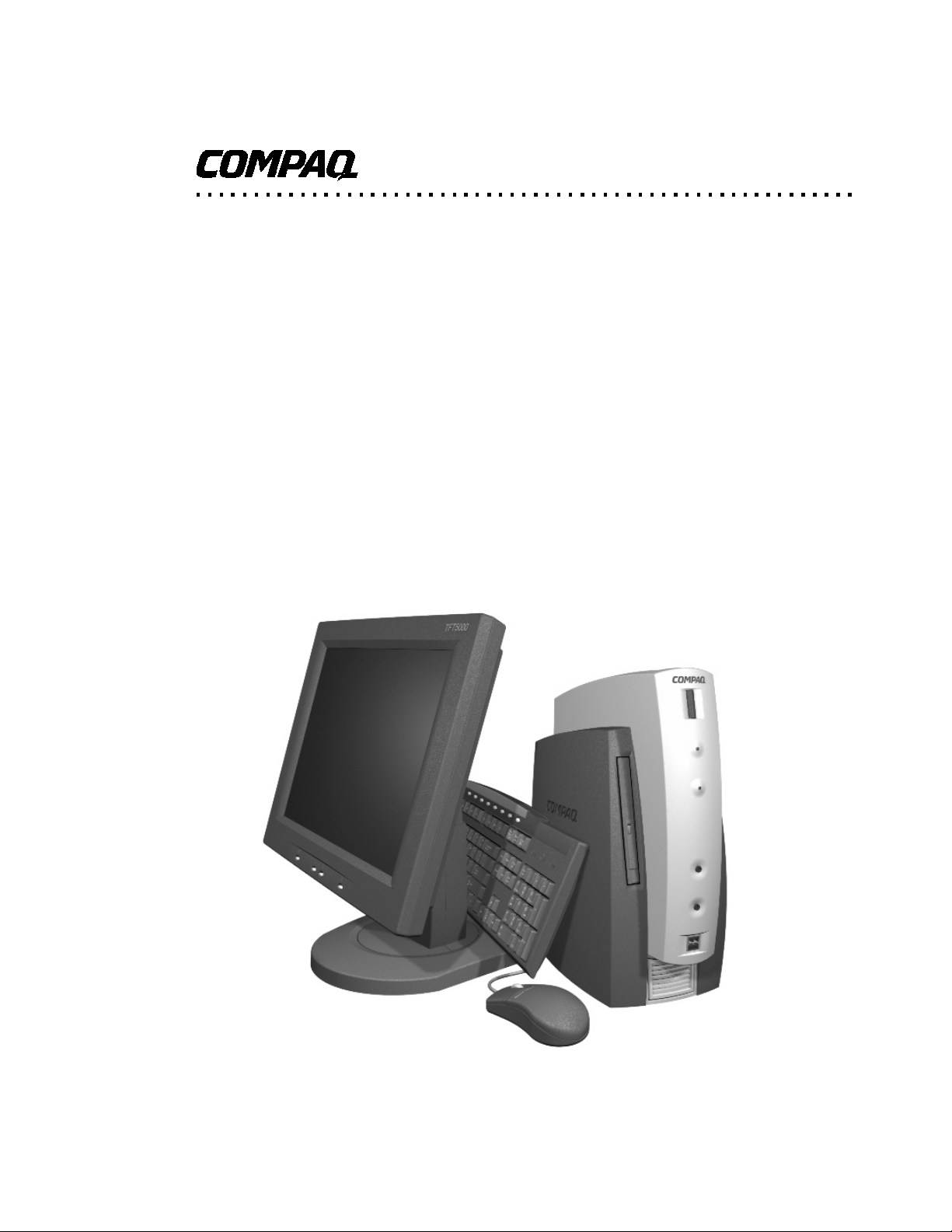
Technical
Reference
Guide
For the
Compaq iPAQ Internet Device
Page 2

This hardcopy is designed to be placed into a standard 3-ring binder. Provided below is a title block that
G
can be copied and cut out and placed into the slip or taped onto the edge of the binder.
iPAQ Internet Device
TR
Page 3

Reader Feedback
Please feel free to send any questions, suggestions, corrections, or comments regarding this
document please to the following email address:
Desktop.training.feedback@Compaq.com
When responding, please state the title of the referenced document.
Page 4

Technical Reference Guide
NOTICE
The information in this document is subject to change without notice.
COMPAQ COMPUTER CORPORATION SHALL NOT BE LIABLE FOR TECHNICAL OR
EDITORIAL ERRORS OR OMISSIONS HEREIN; NOR FOR INCIDENTAL OR
CONSEQUENTIAL DAMAGES RESULTING FROM THE FURNISHING, PERFORMANCE,
OR USE OF THIS MATERIAL. IT IS THE RESPONSIBILITY OF MANUFACTURERS TO
ENSURE THAT DEVICES DESIGNED TO BE USED WITH COMPAQ PRODUCTS
COMPLY WITH FCC CLASS B EMISSIONS REQUIREMENTS.
This guide contains information protected by copyright. Except for use as a reference for the
described Compaq product, no part of this document may be photocopied or reproduced in any
form without prior written consent from Compaq Computer Corporation.
2000 Compaq Computer Corporation
All rights reserved.
Compaq and the Compaq logo are regiserted in the U.S. Patent and Trademark Office.
iPAQ is a trademark of Compaq Information Technologies Group, L.P.
Microsoft, Windows, Windows NT, and other names of Microsoft products referenced herein are trademarks or registered
trademarks of Microsoft Corporation.
Intel and Pentiu m are registered trademarks of Intel Corporation. Celeron and MMX are trademarks of Intel Corporation.
Product names mentioned in this document may be trademarks and/or registered trademarks of other companies.
For more information regarding specifications and Compaq-specific parts please contact Compaq
Computer Corporation at http://www.compaq.com .
Technical Reference Guide
For the
Compaq iPAQ Internet Device
First Edition – March 2000
Document Number 127M-0300A-WWEN
Compaq iPAQ Family of Internet Devices
First Edition - March 2000
i
Page 5

Technical Reference Guide
ii
Compaq iPAQ Family of Internet Devices
First Edition –- March 2000
Page 6

Technical Reference Guide
TABLE OF CONTENTS
CHAPTER 1 INTRODUCTION.............................................................................................................
1.1 ABOUT THIS GUIDE ........................................................................................................... 1-1
1.1.1 USING THIS GUIDE .....................................................................................................1-1
1.1.2 ADDITIONAL INFORMATION SOURCES.................................................................. 1-1
MODEL NUMBERING CONVENTION........................................................................................... 1-1
1.3 NOTATIONAL CONVENTIONS.......................................................................................... 1-2
1.3.1 VALUES........................................................................................................................ 1-2
1.3.2 RANGES........................................................................................................................ 1-2
1.3.3 SIGNAL LABELS.......................................................................................................... 1-2
1.3.4 REGISTER NOTATION AND USAGE ......................................................................... 1-2
1.3.5 BIT NOTATION............................................................................................................ 1-2
1.4 COMMON ACRONYMS AND ABBREVIATIONS.............................................................. 1-3
CHAPTER 2 SYSTEM OVERVIEW.....................................................................................................
2.1 INTRODUCTION.................................................................................................................. 2-1
2.2 FEATURES AND OPTIONS ................................................................................................. 2-2
2.2.1 STANDARD FEATURES .............................................................................................. 2-2
2.2.2 OPTIONS....................................................................................................................... 2-3
2.3 MECHANICAL DESIGN...................................................................................................... 2-4
2.3.1 CABINET LAYOUTS.................................................................................................... 2-4
2.3.2 CHASSIS LAYOUT....................................................................................................... 2-6
2.3.3 SYSTEM BOARD LAYOUTS ....................................................................................... 2-7
2.4 SYSTEM ARCHITECTURE.................................................................................................. 2-8
2.4.1 PROCESSORS ............................................................................................................. 2-10
2.4.2 CHIPSET ..................................................................................................................... 2-12
2.4.3 SUPPORT COMPONENTS.......................................................................................... 2-13
2.4.4 SYSTEM MEMORY.................................................................................................... 2-13
2.4.5 MASS STORAGE ........................................................................................................ 2-14
2.4.6 SERIAL AND PARALLEL INTERFACES .................................................................. 2-14
2.4.7 UNIVERSAL SERIAL BUS INTERFACE ................................................................... 2-14
2.4.8 GRAPHICS SUBSYSTEM........................................................................................... 2-14
2.4.9 AUDIO SUBSYSTEM ................................................................................................. 2-15
2.5 SPECIFICATIONS .............................................................................................................. 2-15
CHAPTER 3 PROCESSOR/MEMORY SUBSYSTEM ........................................................................
3.1 INTRODUCTION.................................................................................................................. 3-1
3.2 PROCESSOR......................................................................................................................... 3-2
3.2.1 CELERON PROCESSOR............................................................................................... 3-2
3.2.2 PENTIUM III PROCESSOR...........................................................................................3-3
3.2.3 PROCESSOR UPGRADING.......................................................................................... 3-4
3.3 MEMORY SUBSYSTEM...................................................................................................... 3-5
3.4 SUBSYSTEM CONFIGURATION ........................................................................................ 3-8
Compaq iPAQ Family of Internet Devices
First Edition - March 2000
iii
Page 7

Technical Reference Guide
CHAPTER 4 SYSTEM SUPPORT.........................................................................................................
4.1 INTRODUCTION.................................................................................................................. 4-1
4.2 PCI BUS OVERVIEW........................................................................................................... 4-2
4.2.1 PCI BUS TRANSACTIONS........................................................................................... 4-3
4.2.2 PCI INTERRUPT MAPPING ......................................................................................... 4-6
4.2.3 PCI POWER MANAGEMENT SUPPORT..................................................................... 4-6
4.2.4 PCI SUB-BUSSES.......................................................................................................... 4-6
4.2.5 PCI CONFIGURATION................................................................................................. 4-7
4.3 AGP BUS OVERVIEW ......................................................................................................... 4-8
4.3.1 BUS TRANSACTIONS.................................................................................................. 4-8
4.3.2 AGP CONFIGURATION ............................................................................................. 4-11
4.4 INTERRUPTS ..................................................................................................................... 4-12
4.4.1 MASKABLE INTERRUPTS ........................................................................................ 4-12
4.4.2 NON-MASKABLE INTERRUPTS............................................................................... 4-14
4.5 INTERVAL TIMER............................................................................................................. 4-16
4.6 SYSTEM CLOCK DISTRIBUTION.................................................................................... 4-16
4.7 REAL-TIME CLOCK AND CONFIGURATION MEMORY............................................... 4-17
4.7.1 CMOS ARCHIVE ........................................................................................................ 4-18
4.7.2 STANDARD CMOS LOCATIONS .............................................................................. 4-18
4.7.3 CMOS FEATURE BITS............................................................................................... 4-26
4.8 SYSTEM MANAGEMENT ................................................................................................. 4-27
4.8.1 SECURITY FUNCTIONS ............................................................................................ 4-27
4.8.2 POWER MANAGEMENT ........................................................................................... 4-28
4.8.3 THERMAL SENSING AND COOLING ...................................................................... 4-28
4.9 SYSTEM I/O MAP.............................................................................................................. 4-29
CHAPTER 5 INPUT/OUTPUT INTERFACES.....................................................................................
5.1 INTRODUCTION.................................................................................................................. 5-1
5.2 ENHANCED IDE INTERFACE ............................................................................................5-1
5.2.1 IDE PROGRAMMING................................................................................................... 5-1
5.2.2 IDE CONNECTOR ........................................................................................................ 5-3
5.3 DISKETTE DRIVE INTERFACE..........................................................................................5-4
5.4 SERIAL INTERFACE ........................................................................................................... 5-5
5.4.1 RS-232 INTERFACE ..................................................................................................... 5-5
5.4.2 SERIAL TEST INTERFACE ........................................................................................5-6
5.4.3 SERIAL INTERFACE PROGRAMMING...................................................................... 5-6
5.5 PARALLEL INTERFACE ..................................................................................................... 5-8
5.5.1 STANDARD PARALLEL PORT MODE ....................................................................... 5-8
5.5.2 ENHANCED PARALLEL PORT MODE....................................................................... 5-9
5.5.3 EXTENDED CAPABILITIES PORT MODE ................................................................. 5-9
5.5.4 PARALLEL INTERFACE PROGRAMMING.............................................................. 5-10
5.5.5 PARALLEL INTERFACE CONNECTOR ................................................................... 5-14
5.6 KEYBOARD/POINTING DEVICE INTERFACE ............................................................... 5-15
5.6.1 KEYBOARD INTERFACE OPERATION ................................................................... 5-15
5.6.2 POINTING DEVICE INTERFACE OPERATION ....................................................... 5-17
5.6.3 KEYBOARD/POINTING DEVICE INTERFACE PROGRAMMING ......................... 5-17
5.6.4 KEYBOARD/POINTING DEVICE INTERFACE CONNECTOR................................ 5-21
iv
Compaq iPAQ Family of Internet Devices
First Edition –- March 2000
Page 8

Technical Reference Guide
5.7 UNIVERSAL SERIAL BUS INTERFACE........................................................................... 5-22
5.7.1 USB DATA FORMATS ............................................................................................... 5-22
5.7.2 USB PROGRAMMING................................................................................................ 5-24
5.7.3 USB CONNECTOR ..................................................................................................... 5-25
5.7.4 USB CABLE DATA..................................................................................................... 5-25
5.8 AUDIO SUBSYSTEM......................................................................................................... 5-26
5.8.1 FUNCTIONAL ANALYSIS ......................................................................................... 5-26
5.8.2 AC97 AUDIO CONTROLLER..................................................................................... 5-28
5.8.3 AC97 LINK BUS ......................................................................................................... 5-28
5.8.4 AUDIO CODEC........................................................................................................... 5-29
5.8.5 AUDIO PROGRAMMING........................................................................................... 5-30
5.8.6 AUDIO SPECIFICATIONS ......................................................................................... 5-31
5.9 NETWORK INTERFACE CONTROLLER.......................................................................... 5-32
5.9.1 WAKE ON LAN.......................................................................................................... 5-33
5.9.2 ALERT ON LAN ......................................................................................................... 5-33
5.9.3 POWER MANAGEMENT SUPPORT.......................................................................... 5-34
5.9.4 NIC PROGRAMMING................................................................................................. 5-35
CHAPTER 6 GRAPHICS SUBSYSTEM...............................................................................................
6.1 INTRODUCTION.................................................................................................................. 6-1
6.2 FUNCTIONAL DESCRIPTION............................................................................................. 6-2
6.2.1 FEATURE SUMMARY ................................................................................................. 6-3
6.3 DISPLAY MODES ................................................................................................................6-4
6.4 UPGRADING ........................................................................................................................ 6-4
6.5 PROGRAMMING..................................................................................................................6-5
6.5.1 CONFIGURATION........................................................................................................ 6-5
6.5.2 CONTROL..................................................................................................................... 6-5
6.6 MONITOR POWER MANAGEMENT CONTROL ............................................................... 6-6
6.7 MONITOR CONNECTOR .................................................................................................... 6-6
CHAPTER 7 POWER SUPPLY AND DISTRIBUTION.......................................................................
7.1 INTRODUCTION.................................................................................................................. 7-1
7.2 POWER SUPPLY ASSEMBLY/CONTROL .......................................................................... 7-1
7.2.1 POWER SUPPLY ASSEMBLY...................................................................................... 7-2
7.2.2 POWER CONTROL....................................................................................................... 7-3
7.3 POWER DISTRIBUTION...................................................................................................... 7-4
7.3.1 3.3/5/12 VDC DISTRIBUTION...................................................................................... 7-4
7.3.2 LOW VOLTAGE DISTRIBUTION................................................................................ 7-4
7.4 SIGNAL DISTRIBUTION ..................................................................................................... 7-5
Compaq iPAQ Family of Internet Devices
First Edition - March 2000
v
Page 9

Technical Reference Guide
CHAPTER 8 BIOS ROM .......................................................................................................................
8.1 INTRODUCTION.................................................................................................................. 8-1
8.2 DESKTOP MANAGEMENT SUPPORT ............................................................................... 8-2
8.2.1 SYSTEM ID................................................................................................................... 8-4
8.2.2 SYSTEM INFORMATION TABLE............................................................................... 8-4
8.2.3 EDID RETRIEVE .......................................................................................................... 8-5
8.2.4 DRIVE FAULT PREDICTION....................................................................................... 8-5
8.2.5 SYSTEM MAP RETRIEVAL......................................................................................... 8-6
8.2.6 FLASH ROM FUNCTIONS........................................................................................... 8-7
8.2.7 POWER BUTTON FUNCTIONS................................................................................... 8-7
8.2.8 ACCESSING CMOS...................................................................................................... 8-8
8.2.9 ACCESSING CMOS FEATURE BITS........................................................................... 8-8
8.2.10 SECURITY FUNCTIONS ............................................................................................ 8-10
8.3 MEMORY DETECTION AND CONFIGURATION............................................................ 8-11
8.4 PNP SUPPORT.................................................................................................................... 8-12
8.4.1 SMBIOS....................................................................................................................... 8-13
8.5 POWER MANAGEMENT FUNCTIONS ............................................................................ 8-14
8.5.1 INDEPENDENT PM SUPPORT .................................................................................. 8-14
8.5.2 ACPI SUPPORT........................................................................................................... 8-15
8.5.3 APM 1.2 SUPPORT ..................................................................................................... 8-15
8.6 USB LEGACY SUPPORT ................................................................................................... 8-17
8.7 BIOS UPGRADING............................................................................................................. 8-18
APPENDIX A ERROR MESSAGES AND CODES...............................................................................
A.1 INTRODUCTION.................................................................................................................A-1
A.2 POWER-ON MESSAGES..................................................................................................... A-1
A.3 BEEP/KEYBOARD LED CODES........................................................................................ A-1
A.4 POWER-ON SELF TEST (POST) MESSAGES.................................................................... A-2
A.5 PROCESSOR ERROR MESSAGES (1
A.6 MEMORY ERROR MESSAGES (2
XX-XX
A.7 KEYBOARD ERROR MESSAGES (30
A.8 PRINTER ERROR MESSAGES (4
XX-XX
A.9 VIDEO (GRAPHICS) ERROR MESSAGES (5
A.10 DISKETTE DRIVE ERROR MESSAGES (6
A.11 SERIAL INTERFACE ERROR MESSAGES (11
A.12 MODEM COMMUNICATIONS ERROR MESSAGES (12
A.13 SYSTEM STATUS ERROR MESSAGES (16
A.14 HARD DRIVE ERROR MESSAGES (17
A.15 HARD DRIVE ERROR MESSAGES (19
A.16 VIDEO (GRAPHICS) ERROR MESSAGES (24
A.17 AUDIO ERROR MESSAGES (3206A.18 DVD/CD-ROM ERROR MESSAGES (33
A.19 NETWORK INTERFACE ERROR MESSAGES (60
A.20 SCSI INTERFACE ERROR MESSAGES (65
A.21 POINTING DEVICE INTERFACE ERROR MESSAGES (8601-
) ...................................................................... A-3
XX-XX
)........................................................................... A-4
) ....................................................................... A-4
X-XX
) ............................................................................ A-5
).......................................................... A-5
XX-XX
) ......................................................... A-6
XX-XX
) ................................................... A-6
XX-XX
).................................... A-7
XX-XX
)........................................................ A-8
XX-XX
) ............................................................... A-8
XX-XX
) ............................................................... A-9
XX-XX
) .................................................... A-9
XX-XX
)......................................................................... A-10
XX
)............................................................ A-10
XX-XX
) ........................................... A-10
XX-XX
, 66XX-XX, 67XX-XX) ....................... A-11
XX-XX
).............................. A-11
XX
A.22 CEMM PRIVILEDGED OPS ERROR MESSAGES........................................................ A-12
A.23 CEMM EXCEPTION ERROR MESSAGES ................................................................... A-12
vi
Compaq iPAQ Family of Internet Devices
First Edition –- March 2000
Page 10

Technical Reference Guide
APPENDIX B ASCII CHARACTER SET .............................................................................................
B.1 INTRODUCTION..................................................................................................................B-1
APPENDIX C KEYBOARD...................................................................................................................
C.1 INTRODUCTION..................................................................................................................C-1
C.2 KEYSTROKE PROCESSING................................................................................................C-2
C.2.1 PS/2-TYPE KEYBOARD TRANSMISSIONS................................................................C-3
C.2.2 USB-TYPE KEYBOARD TRANSMISSIONS................................................................C-4
C.2.3 KEYBOARD LAYOUTS ...............................................................................................C-5
C.2.4 KEYS.............................................................................................................................C-8
C.2.5 KEYBOARD COMMANDS.........................................................................................C-11
C.2.6 SCAN CODES .............................................................................................................C-11
C.3 CONNECTORS ...................................................................................................................C-15
Compaq iPAQ Family of Internet Devices
First Edition - March 2000
vii
Page 11

Technical Reference Guide
LIST OF FIGURES
F
IGURE
F
IGURE
F
IGURE
F
IGURE
F
IGURE
F
IGURE
F
IGURE
F
IGURE
F
IGURE
F
IGURE
F
IGURE
F
IGURE
F
IGURE
F
IGURE
F
IGURE
F
IGURE
F
IGURE
F
IGURE
F
IGURE
F
IGURE
F
IGURE
F
IGURE
F
IGURE
F
IGURE
F
IGURE
F
IGURE
F
IGURE
F
IGURE
F
IGURE
F
IGURE
F
IGURE
F
IGURE
F
IGURE
2–1. C
2–2. C
2–3. C
2–4. C
2–5. C
2–6. C
2–7. P
3–1. P
3–2. C
3–3. P
3–4. S
OMPAQ I
OMPAQ I
OMPAQ I
OMPAQ I
OMPAQ I
OMPAQ I
ROCESSOR ASSEMBLY AND MOUNTING
ROCESSOR/MEMORY SUBSYSTEM ARCHITECTURE
ELERON PROCESSOR INTERNAL ARCHITECTURE
ENTIUM
YSTEM MEMORY MAP
4-1. PCI B
4-2. T
YPE
4-3. PCI C
4-4. AGP 1X D
4-5. AGP 2X D
4-6. M
4-7. C
5-1.
5-2.
5-3.
5-4.
5-5.
5-6.
5-7.
5-8.
5-9.
5-10.
5-11.
5-12.
5-13.
5-14.
5-15.
ASKABLE INTERRUPT PROCESSING
ONFIGURATION MEMORY MAP
40-P
50-P
SERIAL INTERFACE CONNECTOR (MALE
SERIAL INTERFACE HEADER (ON LEGACY-FREE SYSTEM BOARD
PARALLEL INTERFACE CONNECTOR (FEMALE
8042-TO-K
KEYBOARD OR POINTING DEVICE INTERFACE CONNECTOR
USB I/F, B
USB P
UNIVERSAL SERIAL BUS CONNECTOR
AUDIO SUBSYSTEM FUNCTIONAL BLOCK DIAGRAM
AC’97 L
AD1881 A
10/100 TX N
ETHERNET
PAQ I
NTERNET DEVICE WITH MONITOR
PAQ I
NTERNET DEVICE
PAQ I
NTERNET DEVICE
PAQ I
NTERNET DEVICE CHASSIS LAYOUT
PAQ S
YSTEM BOARD LAYOUTS
PAQ A
RCHITECTURE
III P
ROCESSOR INTERNAL ARCHITECTURE
, F
, R
, B
LOCK DIAGRAM
..................................................................................................... 3-7
US DEVICES AND FUNCTIONS
0 C
ONFIGURATION CYCLE
ONFIGURATION SPACE MAP
ATA TRANSFER (PEAK TRANSFER RATE
ATA TRANSFER (PEAK TRANSFER RATE
..................................................................................... 4-2
......................................................................................... 4-4
...................................................................................... 4-5
....................................................................................... 4-17
IN PRIMARY
IN SECONDARY
ACKET FORMATS
IDE C
ONNECTOR (ON SYSTEM BOARD
IDE C
ONNECTOR (ON SYSTEM AND DAUGHTER BOARDS
EYBOARD TRANSMISSION OF CODE EDH
LOCK DIAGRAM
............................................................................................... 5-22
.................................................................................................... 5-23
INK BUS PROTOCOL
UDIO CODEC FUNCTIONAL BLOCK DIAGRAM
ETWORK INTERFACE CONTROLLER BLOCK DIAGRAM
TPE C
ONNECTOR
.......................................................................................... 5-28
(RJ-45,
............................................................. 2-1
RONT VIEW
EAR VIEWS
................................................................ 2-4
................................................................ 2-5
......................................................................... 2-7
.............................................................. 2-9
.......................................................................... 2-11
............................................................ 3-1
............................................................... 3-2
: 266 MB/S)........................................... 4-9
: 532 MB/S)......................................... 4-10
, B
LOCK DIAGRAM
DB-9
AS VIEWED FROM REAR O F CHASSIS
DB-25
, T
.............................................................................. 5-25
VIEWED FROM CARD EDGE
, R
IDE SIDE VIEW
................................ 2-6
........................................................... 3-3
..................................................... 4-12
)...................................................... 5-3
)....................... 5-4
) ...............5-5
)........................................... 5-6
AS VIEWED FROM REAR O F CHASSIS
IMING DIAGRAM
............................. 5-15
).... 5-14
................................................ 5-21
......................................................... 5-27
................................................... 5-29
................................... 5-32
)..................................... 5-36
F
F
F
F
F
F
F
viii
6-1. G
IGURE
6-2. 82810E/DC-100 I
IGURE
7–1.
IGURE
7–2. P
IGURE
7–3. S
IGURE
7–4. H
IGURE
B–1. ASCII C
IGURE
RAPHICS SUBSYSTEM BLOCK DIAGRAM
NTEGRATED GRAPHICS CONTROLLER
POWER DISTRIBUTION AND CONTROL
OWER CABLE DIAGRAM
IGNAL DISTRIBUTION DIAGRAM
EADER PINOUTS
HARACTER SET
............................................................................................................. 7-6
Compaq iPAQ Family of Internet Devices
............................................................................ 6-2
....................................................... 6-3
, B
LOCK DIAGRAM
..................................................... 7-1
.................................................................................................. 7-4
....................................................................................... 7-5
...................................................................................................B-1
First Edition –- March 2000
Page 12

Technical Reference Guide
F
IGURE
F
IGURE
F
IGURE
F
IGURE
F
IGURE
F
IGURE
F
IGURE
F
IGURE
F
IGURE
C–1. K
EYSTROKE PROCESSING ELEMENTS
C–2. PS/2 K
C–3. U.S. E
C–4. N
ATIONAL
C–5. U.S. E
C–6. N
C–7. E
ATIONAL WINDOWS
ASY ACCESS KEY POSITIONS
C–8. PS/2 K
C–9. USB K
, B
LOCK DIAGRAM
EYBOARD-TO-SYSTEM TRANSMISSION
NGLISH
NGLISH WINDOWS
(101-KEY) K
(102-KEY) K
(102W-KEY) K
EYBOARD KEY POSITIONS
EYBOARD KEY POSITIONS
(101W-KEY) K
EYBOARD KEY POSITIONS
EYBOARD KEY POSITIONS
..........................................................................................C-7
EYBOARD CABLE CONNECTOR (MALE
EYBOARD CABLE CONNECTOR (MALE
....................................................C-2
, T
IMING DIAGRAM
......................................C-3
.......................................................C-5
............................................................C-5
...................................C-6
........................................C-6
).................................................................C-15
).................................................................C-15
Compaq iPAQ Family of Internet Devices
First Edition - March 2000
ix
Page 13

Technical Reference Guide
T
1–1. A
ABLE
CRONYMS AND ABBREVIATIONS
LIST OF TABLES
....................................................................................... 1-3
2-1. F
T
ABLE
2-2. A
T
ABLE
2-3. I
T
ABLE
2-4. S
T
ABLE
2-5. E
T
ABLE
2-6. E
T
ABLE
2-7. P
T
ABLE
2-8. M
T
ABLE
2-9. M
T
ABLE
2-10. H
T
ABLE
3–1. C
T
ABLE
3–2. P
T
ABLE
3–3. SPD A
T
ABLE
3–4. H
T
ABLE
4-1. PCI D
T
ABLE
4-2. S
T
ABLE
4-3. LPC B
T
ABLE
4-4. PCI/AGP B
T
ABLE
4-5. M
T
ABLE
4-6. M
T
ABLE
4-7. I
T
ABLE
4-8. I
T
ABLE
4-9. C
T
ABLE
4-10. C
T
ABLE
4-11. S
T
ABLE
EATURE DIFFERENCE MATRIX
RCHITECTURAL COMPARISON
810E C
NTEL
UPPORT COMPONENT FUNCTIONS
NVIRONMENTAL SPECIFICATIONS
LECTRICAL SPECIFICATIONS
HYSICAL SPECIFICATIONS
ULTIBAY 24X
ULTIBAY 24X
ARD DRIVE SPECIFICATIONS
ELERON PROCESSOR STATISTICAL COMPARISON
ENTIUM
/PCI B
OST
YSTEM BOARD
ASKABLE INTERRUPT PRIORITIES AND ASSIGNMENTS
ASKABLE INTERRUPT CONTROL REGISTERS
NTERVAL TIMER FUNCTIONS
NTERVAL TIMER CONTROL REGISTERS
LOCK GENERATION AND DISTRIBUTION
ONFIGURATION MEMORY
YSTEM
HIPSET COMPARISON
CD-ROM D
CD-ROM D
III P
ROCESSOR STATISTICAL COMPARISON
DDRESS MAP
EVICE CONFIGURATION ACCESS
RIDGE CONFIGURATION REGISTERS
RIDGE CONFIGURATION REGISTERS
(SDRAM DIMM)................................................................................. 3-6
RIDGE CONFIGURATION REGISTERS
PCI D
EVICE IDENTIFICATION
I/O MAP........................................................................................................... 4-29
........................................................................................... 2-2
............................................................................................. 2-8
.................................................................................... 2-12
.................................................................................... 2-13
.................................................................................... 2-15
............................................................................................ 2-15
................................................................................................ 2-16
RIVE SPECIFICATIONS
RIVE SPECIFICATIONS
......................................................................................... 2-17
(GMCH, F
................................................................................. 4-4
..................................................................... 4-5
(ICH, F
(MCH, F
.................................................................... 4-13
............................................................................................ 4-16
............................................................................. 4-16
........................................................................... 4-16
(CMOS) MAP....................................................................... 4-18
............................................................. 2-16
............................................................. 2-17
............................................................... 3-2
........................................................... 3-3
0)................................ 3-8
1) .................................. 4-11
UNCTION
UNCTION
UNCTION
0).............................................. 4-7
...................................................... 4-13
5–1. IDE PCI C
T
ABLE
5–2.
T
ABLE
T
ABLE
T
ABLE
T
ABLE
T
ABLE
T
ABLE
T
ABLE
T
ABLE
T
ABLE
T
ABLE
T
ABLE
T
ABLE
T
ABLE
T
ABLE
T
ABLE
T
ABLE
T
ABLE
x
Compaq iPAQ Family of Internet Devices
IDE B
5–3. 40-P
5–4. 50-P
5–5.
DB-9 S
5–6. S
5–7. S
5–8. P
5–9.
ERIAL INTERFACE CONFIGURATION REGISTERS
ERIAL INTERFACE CONTROL REGISTERS
ARALLEL INTERFACE CONFIGURATION REGISTERS
PARALLEL INTERFACE CONTROL REGISTERS
5–10. DB-25 P
5–11. 8042-TO-K
5–12. K
EYBOARD INTERFACE CONFIGURATION REGISTERS
5–13. CPU C
5–14. K
EYBOARD/POINTING DEVICE CONNECTOR PINOUT
5–15. USB I
5–16. USB C
5–17. USB C
5–18. USB C
ONFIGURATION REGISTERS
US MASTER CONTROL REGISTERS
IN PRIMARY
IN SECONDARY
ERIAL CONNECTOR PINOUT
OMMANDS TO THE
NTERFACE CONFIGURATION REGISTERS
ONTROL REGISTERS
ONNECTOR PINOUT
ABLE LENGTH DATA
IDE C
ONNECTOR PINOUT
IDE C
ARALLEL CONNECTOR PINOUT
EYBOARD COMMANDS
................................................................................ 5-2
.............................................................................. 5-2
......................................................................... 5-3
ONNECTOR PINOUT
.................................................................... 5-4
...................................................................................... 5-5
.................................................................. 5-6
............................................................................ 5-7
........................................................... 5-10
...................................................................... 5-11
.......................................................................... 5-14
.................................................................................. 5-16
....................................................... 5-17
8042...................................................................................... 5-19
........................................................ 5-21
................................................................. 5-24
............................................................................................. 5-24
.............................................................................................. 5-25
............................................................................................ 5-25
First Edition –- March 2000
Page 14

T
5–19. AC’97 A
ABLE
5–20. AC’97 A
T
ABLE
5–21. A
T
ABLE
5–22. AOL E
T
ABLE
5–23. NIC C
T
ABLE
5–24. NIC C
T
ABLE
5–25. 82559 NIC O
T
ABLE
UDIO CONTROLLER
UDIO CODEC CONTROL REGISTERS
UDIO SUBSYSTEM SPECIFICATIONS
................................................................................................................ 5-33
VENTS
ONTROLLER
ONTROL REGISTERS
PCI C
PERATING SPECIFICATIONS
PCI C
ONFIGURATION REGISTERS
............................................................................................. 5-35
Technical Reference Guide
ONFIGURATION REGISTERS
........................................ 5-30
................................................................... 5-30
............................................................................... 5-31
....................................................... 5-35
........................................................................ 5-36
6-1. I
T
ABLE
T
ABLE
T
ABLE
T
ABLE
T
ABLE
T
ABLE
T
ABLE
T
ABLE
T
ABLE
T
ABLE
T
ABLE
T
ABLE
T
ABLE
T
ABLE
T
ABLE
T
ABLE
T
ABLE
T
ABLE
T
ABLE
T
ABLE
T
ABLE
T
ABLE
T
ABLE
T
ABLE
T
ABLE
T
ABLE
T
ABLE
T
ABLE
T
ABLE
T
ABLE
T
ABLE
NTEL GRAPHICS DISPLAY MODES
6-2. PCI C
6-3. S
TANDARD
6-4. M
ONITOR POWER MANAGEMENT CONDITIONS
6-5. DB-15 M
8-1. D
ESKTOP MANAGEMENT FUNCTIONS
8-2. CMOS F
8-3. PNP BIOS F
8-4. APM BIOS F
A–1. P
A–2. B
A–3. P
A–4. S
A–5. M
A–6. K
A–7. P
A–8. V
A–9. D
A–10. S
A–11. S
A–12. S
A–13. H
A–14. H
A–15. H
A–16. A
OWER-ON MESSAGES
EEP/KEYBOARD
OWER-ON SELF TEST
YSTEM ERROR MESSAGES
EMORY ERROR MESSAGES
EYBOARD ERROR MESSAGES
RINTER ERROR MESSAGES
IDEO (GRAPHICS
ISKETTE DRIVE ERROR MESSAGES
ERIAL INTERFACE ERROR MESSAGES
ERIAL INTERFACE ERROR MESSAGES
YSTEM STATUS ERROR MESSAGES
ARD DRIVE ERROR MESSAGES
ARD DRIVE ERROR MESSAGES
ARD DRIVE MESSAGES
UDIO ERROR MESSAGES
A–17. DVD/CD-ROM D
A–18. N
ETWORK INTERFACE ERROR MESSAGES
A–19. SCSI I
A–20. P
OINTING DEVICE INTERFACE ERROR MESSAGES
A–21. CEMM P
A–22. CEMM E
....................................................................................... 6-4
ONFIGURATION SPACE REGISTERS
VGA M
ONITOR CONNECTOR PINOUT
ODE
I/O M
APPING
(INT15)..................................................................... 8-2
EATURE BITS
UNCTIONS
UNCTIONS
........................................................................................................ 8-9
..................................................................................................... 8-12
(INT15) ...................................................................................... 8-17
..................................................................................................... A-1
LED C
.......................................................................................... A-1
ODES
(POST) M
ESSAGES
............................................................................................... A-3
............................................................................................. A-4
.......................................................................................... A-4
.............................................................................................. A-5
) E
RROR MESSAGES
.................................................................................. A-6
...................................................................................... A-8
...................................................................................... A-9
................................................................................................. A-9
............................................................................................. A-10
RIVE ERROR MESSAGES
NTERFACE ERROR MESSAGES
RIVILEGED OPS ERROR MESSAGES
XCEPTION ERROR MESSAGES
.............................................................................. 6-5
................................................................................ 6-5
.................................................................... 6-6
................................................................................ 6-6
........................................................................ A-2
.............................................................................. A-5
............................................................................. A-6
............................................................................. A-7
................................................................................ A-8
.................................................................... A-10
...................................................................... A-10
............................................................................. A-11
........................................................... A-11
.................................................................. A-12
......................................................................... A-12
T
ABLE
T
ABLE
C–1. K
C–2. K
EYBOARD-TO-SYSTEM COMMANDS
EYBOARD SCAN CODES
.................................................................................................C-12
...............................................................................C-11
Compaq iPAQ Family of Internet Devices
First Edition - March 2000
xi
Page 15

Technical Reference Guide
xii
Compaq iPAQ Family of Internet Devices
First Edition –- March 2000
Page 16

Chapter 1
INTRODUCTION
Technical Reference Guide
1.
Chapter 1 INTRODUCTION
1.1 ABOUT THIS GUIDE
This guide provides technical information about the Compaq iPAQ Family of Internet Devices.
This document includes information regarding system design, function, and features that can be
used by programmers, engineers, technicians, and system administrators.
This guide and any applicable addendum are available online at the following location:
http://www.compaq.com/support/techpubs/technical_reference_guides/index.html
1.1.1 USING THIS GUIDE
The chapters of this guide primarily describe the hardware and firmware elements and primarily
deal with the system board and the power supply assembly. The appendices contain general
information about standard peripheral devices such as the keyboard.
1.1.2 ADDITIONAL INFORMATION SOURCES
For more information on chipset components mentioned in this guide refer to the indicated
manufacturers’ documentation, which may be available at the following online sources:
♦
Compaq Computer Corporation: http://www.compaq.com
♦
Intel Corporation: http://www.intel.com
♦
Standard Microsystems Corporation: http://www.smsc.com
1.2 MODEL NUMBERING CONVENTION
The model numbering convention for Compaq iPAQ units is as follows:
iPAQ/XNNN/Nb/N/NNN
Memory (in MB)
Operating system: 4 = Win NT 4.0; 9 = Win95/98
Chipset type (b = 810e)
Hard drive size (in GB)
Processor speed (in MHz)
Processor type: C = Celeron; P = Pentium
Compaq iPAQ Family of Internet Devices
1-1
First Edition - March 2000
Page 17

Chapter 1 Introduction
1.3 NOTATIONAL CONVENTIONS
1.3.1 VALUES
Hexadecimal values are indicated by a numerical or alpha-numerical value followed by the letter
“h.” Binary values are indicated by a value of ones and zeros followed by the letter “b.”
Numerical values that have no succeeding letter can be assumed to be decimal.
1.3.2 RANGES
Ranges or limits for a parameter are shown using the following methods:
Example A: Bits <7..4> = bits 7, 6, 5, and 4.
Example B: IRQ3-7, 9 = IRQ signals 3 through 7, and IRQ signal 9
1.3.3 SIGNAL LABELS
Signal names are indicated using abbreviations, acronyms, or, if possible, the full signal name in
all capital letters. Signals that are meant to be active (asserted) low are indicated with a dash
immediately following the name.
1.3.4 REGISTER NOTATION AND USAGE
This guide uses standard Intel naming conventions in discussing the microprocessor’s (CPU)
internal registers. Registers that are accessed through programmable I/O using an indexing
scheme are indicated using the following format:
03C5.17h
Index port
Data port
In the example above, register 03C5.17h is accessed by writing the index port value 17h to the
index address (03C4h), followed by a write to or a read from port 03C5h.
1.3.5 BIT NOTATION
Bit values are labeled with bit <0> representing the least-significant bit (LSb) and bit <7>
representing the most-significant bit (MSb) of a byte. Bytes, words, double words, and quad
words are typically shown with most-significant portions on the left or top and the leastsignificant portions on the right or bottom respectively.
1-2
Compaq iPAQ Family of Internet Devices
First Edition – March 2000
Page 18

1.4 COMMON ACRONYMS AND ABBREVIATIONS
Table 1-1 lists the acronyms and abbreviations used in this guide.
Technical Reference Guide
Table 1–1.
Acronyms and Abbreviations
Table 1-1.
Acronyms and Abbreviations
Acronym/Abbreviation Description
A ampere
AC alternating current
ACPI Advanced Configuration and Power Interface
A/D analog-to-digital
AGP Accelerated graphics port
API application programming interface
APM advanced power management
AOL Alert-ON-LAN
ASIC application-specific integrated circuit
AT 1) attention (modem commands) 2) 286-based PC architecture
ATA AT attachment (IDE protocol)
ATAPI AT attachment w/packet interface extensions
AVI audio-video interleaved
AVGA Advanced VGA
BAT Basic assurance test
BCD binary-coded decimal
BIOS basic input/output system
bis second/new revision
BitBLT bit block transfer
BNC Bayonet Neill-Concelman (connector)
bps or b/s bits per second
BSP Bootstrap processor
BTO Built to order
CAS column address strobe
CD compact disk
CD-ROM compact disk read-only memory
CDS compact disk system
CF carry flag
CGA color graphics adapter
Ch channel
cm centimeter
CMC cache/memory controller
CMOS complimentary metal-oxide semiconductor (configuration memory)
Cntlr controller
Cntrl control
codec compressor/decompressor
CPQ Compaq
CPU central processing unit
CRT cathode ray tube
CSM Compaq system management / Compaq server management
CTO Configure to order
DAA direct access arrangement
DAC digital-to-analog converter
DC direct current
DCH DOS compatibility hole
DDC Display Data Channel
DF direction flag
Continued
Compaq iPAQ Family of Internet Devices
First Edition - March 2000
1-3
Page 19

Chapter 1 Introduction
Table 1-1.
Acronym/Abbreviation Description
DIMM dual inline memory module
DIN Deutche IndustriNorm (connector standard)
DIP dual inline package
DMA direct memory access
DMI Desktop management interface
dpi dots per inch
DRAM dynamic random access memory
DRQ data request
EDID extended display identification data
EDO extended data out (RAM type)
EEPROM electrically eraseable PROM
EGA enhanced graphics adapter
EIA Electronic Industry Association
EISA extended ISA
EPP enhanced parallel port
EIDE enhanced IDE
ESCD Extended System Configuration Data (format)
EV Environmental Variable (data)
ExCA Exchangeable Card Architecture
FIFO first in / first out
FL flag (register)
FM frequency modulation
FPM fast page mode (RAM type)
FPU Floating point unit (numeric or math coprocessor)
FPS Frames per second
ft foot
GB gigabyte
GMCH Graphics/memory controller hub
GND ground
GPIO general purpose I/O
GPOC general purpose open-collector
GART Graphics address re-mapping table
GUI graphics user interface
h hexadecimal
HW hardware
hex hexadecimal
Hz hertz
ICH I/O controller hub
IDE integrated drive element
IEEE Institute of Electrical and Electronic Engineers
IF interrupt flag
I/F interface
in inch
INT interrupt
I/O input/output
IPL initial program loader
IrDA InfraRed Data Association
IRQ interrupt request
ISA industry standard architecture
JEDEC Joint Electron Device Engineering Council
Kb / KB kilobits / kilobytes (x 1024 bits / x 1024 bytes)
Kb/s kilobits per second
kg kilogram
KHz kilohertz
kv kilovolt
Acronyms and Abbreviations
Continued
Continued
1-4
Compaq iPAQ Family of Internet Devices
First Edition – March 2000
Page 20

Technical Reference Guide
Table 1-1.
Acronym/Abbreviation Description
lb pound
LAN local area network
LCD liquid crystal display
LED light-emitting diode
LIF low insertion force (socket)
LPC Low pin count
LSI large scale integration
LSb / LSB least significant bit / least significant byte
LUN logical unit (SCSI)
MCH Memory controller hub
MMX multimedia extensions
MPEG Motion Picture Experts Group
ms millisecond
MSb / MSB most significant bit / most significant byte
mux multiplex
MVA motion video acceleration
MVW motion video window
n
NIC network interface card/controller
NiCad nickel cadmium
NiMH nickel-metal hydride
NMI non-maskable interrupt
NRZI Non-return-to-zero inverted
ns nanosecond
NT nested task flag
NTSC National Television Standards Committee
NVRAM non-volatile random access memory
OEM original equipment manufacturer
OS operating system
PAL 1. programmable array logic 2. phase altering line
PC Internet Device
PCI peripheral component interconnect
PCM pulse code modulation
PCMCIA Internet Device Memory Card International Association
PF parity flag
PIN personal identification number
PIO Programmed I/O
POST power-on self test
PROM programmable read-only memory
PTR pointer
RAM random access memory
RAS row address strobe
rcvr receiver
RF resume flag
RGB red/green/blue (monitor input)
RH Relative humidity
RIMM RDRAM inline memory module
RMS root mean square
ROM read-only memory
RPM revolutions per minute
RTC real time clock
R/W read/write
Acronyms and Abbreviations
variable parameter/value
Continued
Continued
Compaq iPAQ Family of Internet Devices
First Edition - March 2000
1-5
Page 21

Chapter 1 Introduction
1-6
Compaq iPAQ Family of Internet Devices
First Edition – March 2000
Page 22

Technical Reference Guide
Table 1-1.
Acronym/Abbreviation Description
SCSI small computer system interface
SDRAM Synchronous Dynamic RAM
SEC Single Edge-Connector
SECAM sequential colour avec memoire (sequential color with memory)
SF sign flag
SGRAM Synchronous Graphics RAM
SIMD Single instruction multiple data
SIMM single in-line memory module
SIT system information table
SMART Self Monitor Analysis Report Technology
SMI system management interrupt
SMM system management mode
SMRAM system management RAM
SPD serial presence detect
SPP standard parallel port
SRAM static RAM
SSE Streaming SIMD extensions
STN super twist pneumatic
SVGA super VGA
SW software
TAD telephone answering device
TAFI Temperature-sensing And Fan control Integrated circuit
TAM telephone answering machine
TCP tape carrier package
TF trap flag
TFT thin-film transistor
TIA Telecommunications Information Administration
TPE twisted pair ethernet
TPI track per inch
TTL transistor-transistor logic
TV television
TX transmit
UART universal asynchronous receiver/transmitter
UDMA Ultra DMA
URL Uniform resource locator
us / µs microsecond
USB Universal Serial Bus
UTP unshielded twisted pair
Vvolt
VESA Video Electronic Standards Association
VGA video graphics adapter
vib vibrato
VLSI very large scale integration
VRAM Video RAM
Wwatt
WOL Wake on LAN
WRAM Windows RAM
ZF zero flag
ZIF zero insertion force (socket)
Acronyms and Abbreviations
Continued
Compaq iPAQ Family of Internet Devices
First Edition - March 2000
1-7
Page 23
Chapter 2
SYSTEM OVERVIEW
2. Chapter 2 SYSTEM OVERVIEW
2.1 INTRODUCTION
The Compaq iPAQ Family of Internet Devices provides affordable business solutions with the
focus on internet access and mainstream performance. Based on an Intel Celeron or Pentium III
processor with the Intel 810e chipset, these systems are designed to maximize the effectiveness of
internet and intranet usage while simplifying system management.
Technical Reference Guide
Figure 2–1.
This chapter includes the following topics:
♦
Features and options (2.2) page 2-2
♦
Mechanical design (2.3) page 2-4
♦
System architecture (2.4) page 2-8
♦
Specifications (2.5) page 2-13
Compaq iPAQ Family of Internet Devices
Compaq iPAQ Internet Device with Monitor
First Edition - March 2000
2-1
Page 24

Chapter 2 System Overview
2.2 FEATURES AND OPTIONS
This section describes the standard features and available options.
2.2.1 STANDARD FEATURES
The following standard features are available on all models:
♦
Celeron or Pentium III processor
♦
810e Chipset
♦
Two DIMM sockets for system memory
♦
AC’97 audio subsystem w/Compaq Premier Sound and front panel mic and headphone jacks
♦
MuliBay device mount w/hot-swap support
♦
Extended IDE controller supporting UATA/66 mode
♦
Hard drive fault prediction
♦
Two USB ports on front panel
♦
Network interface controller
♦
VGA analog output (1600 x 1200 max resolution)
♦
APM 1.2 power management support
♦
Plug ’n Play compatible (with ESCD support)
♦
Intelligent Manageability support
♦
Energy Star compliant
♦
Security features including:
•
Setup and power-on passwords
•
DriveLock for MultiBay hard drive
•
I/O interface disabling
•
Administrator password
•
Network service boot
•
Asset tracking tag
•
UUID
•
Cable lock provision
♦
Compaq Easy-Access keyboard w/Windows support
♦
Mouse
Table 2-1 shows the differences in features between the iPAQ models:
Table 2-1.
4-MB Display cache No Yes No Yes
Rear panel USB ports 3 3 0 0
Serial port 0 0 1 1
Parallel port 0 0 1 1
Keyboard/mouse connection USB USB PS/2 PS/2
Feature Difference Matrix
2-2
Compaq iPAQ Family of Internet Devices
Table 2-1.
iPAQ Feature Difference Matrix
Legacy-Free Legacy-Light
Celeron-Based Pentium-based Celeron-Based Pentium-Based
First Edition – March 2000
Page 25

2.2.2 OPTIONS
The following items are available as options for all models and may be included in the standard
configuration of some models:
♦
System Memory: 32-MB DIMM (non-ECC)
♦
Hard drives: 4.3 or 8.4 GB UATA/66 hard drive
♦
MultiBay drives: 24x CD-ROM drive
Technical Reference Guide
64-MB DIMM (non-ECC)
128-MB DIMM (non-ECC)
256-MB DIMM (non-ECC)
4x DVD-ROM drive
Super Disk LS-120 Power Drive
6.0 GB hard drive
Compaq iPAQ Family of Internet Devices
First Edition - March 2000
2-3
Page 26
Chapter 2 System Overview
2.3 MECHANICAL DESIGN
The Compaq iPAQ Internet Device uses a minitower form factor featuring a smaller footprint
and reduced height than previous minitowers, allowing easy floor or desktop positioning.
Commonly used audio and USB connections are accessible from the front panel. There are slight
differences between the legacy-light and legacy-free models, most notably in the rear panel
layouts.
NOTE:
For detailed information on servicing the Internet Device refer to the applicable
Maintenance and Service Guide.
2.3.1 CABINET LAYOUTS
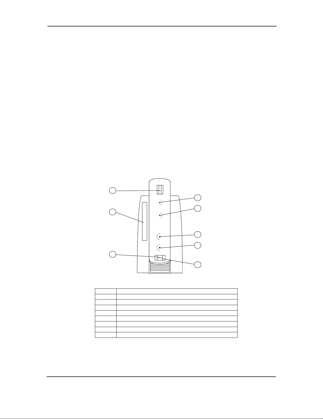
2.3.1.1 Front View
1
4
7
2
3
5
6
Item Description
1 Power Button
2 Power LED
3 Hard drive activity LED
4 MultiBay device bay (accepts 5.25”/12.7 mm storage device)
5 Microphone In Jack
6 Headphone Out Jack
7 USB port 3 jack
8 USB port 4 jack
Figure 2–2.
2-4
Compaq iPAQ Family of Internet Devices
Compaq iPAQ Internet Device, Front View
8
First Edition – March 2000
Page 27
2.3.1.2 Rear Views
Technical Reference Guide
1
3
5
7
11
13
Item Description Item Description
1 Audio line output 2 Audio line input
3 Network activity LED indicator 4 Network I/F jack
5 Network speed LED indicator 6 VGA monitor connector
7 Parallel I/F connector 8 Serial I/F connector
9 USB port connectors (left-to-right; 0,1, 2) 10 MultiBay device eject button
11 PS/2 mouse connector 12 PS/2 keyboard connector
13 AC line in connector 14 Line voltage select switch
2
4
6
8
10
12
14
13
1
3
5
9
2
4
6
10
14
Legacy-FreeLegacy-Light
Figure 2–3.
Compaq iPAQ Internet Device, Rear Views
Compaq iPAQ Family of Internet Devices
First Edition - March 2000
2-5
Page 28
Chapter 2 System Overview
2.3.2 CHASSIS LAYOUT
The internal assemblies are accessible from the right side of the system unit. The right side
(carbon-colored) cover is easily removable allowing quick access to the DIMM sockets through
an access opening and to the hard drive. Access to the system board and processor requires
removing the right chassis access panel.
NOTE:
For a detailed description on servicing the unit refer to the applicable
Maintenance and Service Guide.
1
2
3
4
5
6
7
8
Right Side Cover Removed Right Side Cover and
Chassis Access Panel Removed
Item Description
1 Power button/LED board (PCA# 010647)
2 DIMM socket access
3 Hard drive in 3.5” 1/3 height bay
4 Audio I/O board (PCA# 010650)
5 System board (PCA# 161014 or 161015)
6 Power supply assembly
7 Processor
8 Speaker
Figure 2–4.
2-6
Compaq iPAQ Family of Internet Devices
Compaq iPAQ Internet Device Chassis Layout, Ride Side View
First Edition – March 2000
Page 29

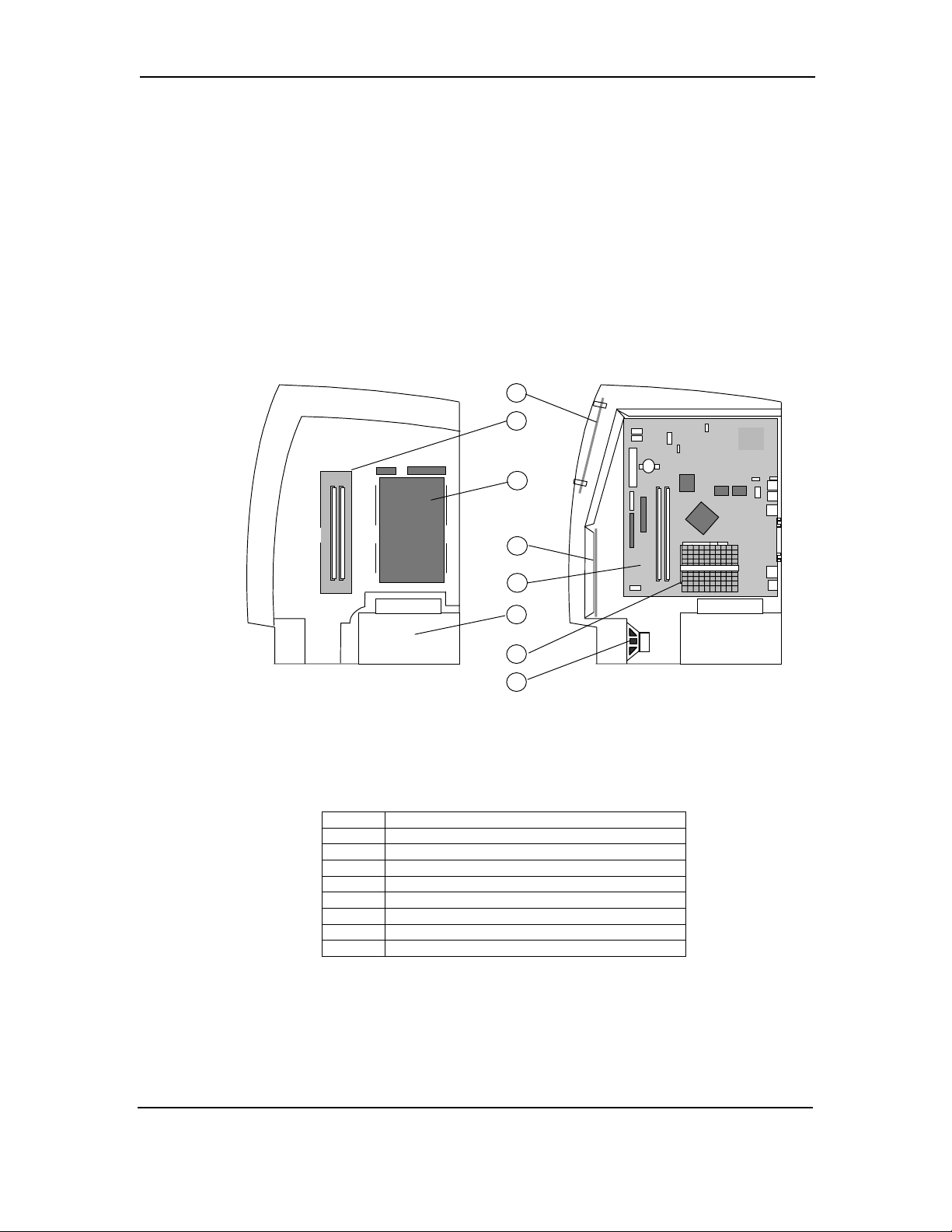
2.3.3 SYSTEM BOARD LAYOUTS
The Compaq iPAQ Internet Device uses a FlexATX-type (9.0 x 7.5 inch) system board. Two
variations are available; a legacy-light board and a legacy-free board.
Technical Reference Guide
1 2 4
22
21
20
19
18
17 1516
Legacy Light (PCA# 161014)
Refer to Chapter 7 “Power and Signal Distribution” for header pinouts.
NOTE:
3
Item Description
1 USB ports 3 and 4 (front panel) header
2 Battery
3 BIOS ROM configuration jumper
4 Speaker connector
5 Audio microphone/headphone header
6 Audio line out jack
7 Audio line in jack
8 Network connector
9 VGA monitor connector
10 Parallel I/F connector
11 Serial I/F connector
12 USB ports 0, 1, 2 connectors
13 PS/2 mouse connector (top), PS/2 keyboard connector (bottom)
14 Serial I/F header
15 PGA370 processor socket
16 DIMM sockets
17 Processor (boxed) fan header
18 IDE (primary) 40-pin connector
19 IDE (secondary) 50-pin connector
20 Power button/LED indicator connector
21 CD audio header
22 Power supply connector
5
22
6
21
7
20
8
9
19
10
11
13
18
1 2 4
17 141516
Legacy Free (PCA# 161015)
3
5
6
7
8
9
12
Figure 2–5.
Compaq iPAQ System Board Layouts
Compaq iPAQ Family of Internet Devices
First Edition - March 2000
2-7
Page 30

Chapter 2 System Overview
2.4 SYSTEM ARCHITECTURE
The Compaq iPAQ Internet Device features an Intel Celeron or Pentium III processor and the
810e chipset. As indicated in the following table and shown in Figure 2-6, four architectural
configurations are available:
♦
Legacy-free with Celeron processor
♦
Legacy-free with Pentium III processor
♦
Legacy-light with Celeron processor
♦
Legacy-light with Pentium III processor
Legacy-free systems provide five Universal Serial Bus (USB) ports for connecting peripherals
(including the supplied USB mouse and USB keyboard). Legacy light systems provide two USB
ports along with the traditional PS/2 connectors for the supplied mouse and keyboard as well as
parallel and serial port connectors.
All systems use the 810e chipset. The 810e chipset includes the 82810e-DC100 GMCH designed
to provide control for SDRAM and also integrates an AGP 2X graphics controller. Pentium IIIbased systems come with an additional 4-MB display cache to compliment the graphics
controller.
The 810e chipset also includes an 82801 I/O Controller Hub (ICH) that provides two IDE
interfaces, two USB interfaces, and a PCI bus controller. The 82802 Firmware Hub (FWH)
component is loaded with Compaq BIOS
Table 2-1 lists differences between system architectures:
Table 2-2.
Architectural Comparison
Table 2-2
.
Architectural Comparison
Host bus (FSB)speed [1] 66 MHz 100 MHz 66 MHz 100 MHz
Celeron-Based Pentium III-Based Celeron-Based Pentium III-Based
4-MB Display Cache? No Yes No Yes
PS/2 Mouse/Keyboard? No No Yes Yes
Serial port? No No Yes Yes
Parallel port? No No Yes Yes
# of USB ports 5 5 2 2
NOTES:
[1] As configured with 500-MHz processor.
Legacy Free Legacy Light
2-8
Compaq iPAQ Family of Internet Devices
First Edition – March 2000
Page 31

Celeron or
y
gacy
y
Pentium III
Processor
66-/100-/133- MHz FSB
Technical Reference Guide
Displa
Monitor
4-MB
Cache
Hard Drive
MultiBay
Subsystem
IDE
Device
Audio
RGB
AGP
2X
Cntlr.
Pri.
IDE I/F
Sec.
IDE I/F
Beep
Audio
AC’97
Audio Bus
810e Chipset
82810e-DC100
GMCH
Hub Link
Bus
82801
ICH
82802
FWH
33-MHz
32-Bit PCI Bus
82559
Ethernet
Controller
SDRAM
Cntlr.
USB
I/F
PC100
Memory
Bus
LPC
Bus
SDRAM
System
Memory
USB
Port 0
LPC47B277 I/O Controller
Serial
I/F
Power
Supply
USB
Port 1
Keyboard/
Mouse I/F
Parallel
I/F
USB
Port 2
USB Hub
USB
Port 3
USB
Port 4
..................
LEGEND:
Legacy-light systems only.
-free systems only.
Le
Pentium III-based s
Figure 2–6.
Compaq iPAQ Architecture, Block diagram
Compaq iPAQ Family of Internet Devices
stems only.
2-9
First Edition - March 2000
Page 32

Chapter 2 System Overview
2.4.1 PROCESSORS
The Compaq iPAQ family includes models based on Celeron and Pentium III processors. These
processors are backward-compatible with software written for the Pentium II, Pentium MMX,
Pentium Pro, Pentium, and x86 microprocessors. Both processor architectures include a floatingpoint unit and first and secondary caches providing enhanced performance for multimedia
applications.
2.4.1.1 Celeron Processor
Select Compaq iPAQ systems use the Intel Celeron processor. The Celeron processor provides
economical performance and is compatible with software written for previous generation
processors such as Pentium II, Pentium MMX, Pentium, and x86 processors. Featuring a
Pentium-type core architecture, the Celeron processor integrates a dual-ALU CPU with a
floating-point unit, 32-KB first-level cache, and 128-KB second level cache, all of which operate
at full processing (CPU) speed. The Celeron processor includes MMX technology for enhanced
multimedia performance.
The Celeron processor uses a PGA370 package with a heat sink.
2.4.1.2 Pentium III Processor
The Intel Pentium III processor used on select systems represents the maximum performance
processor for Compaq iPAQs. The Pentium III processor is compatible with software written for
Celeron, Pentium II, Pentium MMX, Pentium, and x86 processors.
The Pentium III processor core integrates a dual-ALU CPU with a floating-point unit and 32-KB
first-level cache operating at processing (CPU) speed. Featuring .18-micron technology, the
Pentium III processor features 256 kilobytes of secondary cache included on the CPU die and
operating at full processor speed.
The Pentium III processor includes MMX technology for enhanced multimedia performance.
Also included are 70 additional streaming SIMD extensions (SSE) for enhancing 3D graphics
and speech processing performance and a serial number function useful for asset tracking.
The Pentium III processor employed in these systems uses a Flip-Chip (FC) PGA370 package
and heat sink.
2-10
Compaq iPAQ Family of Internet Devices
First Edition – March 2000
Page 33

2.4.1.3 Processor Upgrading
All models of the Compaq iPAQ use the PGA370 zero-insertion force (ZIF) socket for processor
mounting as shown in Figure 2-7. Raising the Lock/Unlock handle of the socket in the vertical
position allows the processor to be removed or inserted into the socket. Lowering the
Lock/Unlock handle in the down (horizontal) position locks the processor in place. Factory
configurations use processors fitted with passive heat sinks. Upgrade (boxed) processors may be
fitted with a heat sink/fan assembly with a power cable that attaches to the fan power header
provided on the system board.
Technical Reference Guide
Heat Sink
Processor
PPGA370
Socket
Lock/Unlock
Figure 2–7.
Heat Sink
Retaining Clip
Handle
Processor Assembly and Mounting
The processor clock frequency is automatically set by chipset logic, eliminating the need for
setting DIP switches when upgrading the processor.
WARNING:
!
of 18 amps. Installing a replacement processor that draws more than 18 amps of current
The system board is designed handle a maximum processor current load
may damage the processor and/or the system board.
Compaq iPAQ Family of Internet Devices
First Edition - March 2000
2-11
Page 34

Chapter 2 System Overview
2.4.2 CHIPSET
The Compaq iPAQ employs the Intel 810e chipset, which is designed to compliment the
processor and provide the central point for the system’s data transactions.
The chipset is composed of a graphics memory controller hub (GMCH), an I/O controller hub
(ICH), and a firmware hub (FWH). Table 2-3 shows the functions provided by the components of
the chipset.
Table 2-3.
Intel 810e Chipset Comparison
Table 2-3.
Intel 810e Chipset Components
Component Type Function
82810e-DC100 Graphics/Memory
Controller Hub(GMCH)
82801AA I/O Controller Hub (ICH) LPC bus I/F
82802 Firmware Controller Hub (FWH) Loaded with Compaq BIOS
AGP 2X graphics controller (i740 equivalent)
SDRAM controller supporting 2 PC100 DIMMs
66-/100-/133-MHz FSB
PCI bus I/F
SMBus I/F
IDE I/F with UATA/66 support
AC ’97 audio controller
RTC/CMOS
IRQ controller
Power management logic
USB I/F (2)
Random number generator
2-12
Compaq iPAQ Family of Internet Devices
First Edition – March 2000
Page 35

2.4.3 SUPPORT COMPONENTS
Input/output functions not provided by the chipset are handled by other support components.
Some of these components also provide “housekeeping” and various other function s as well.
Table 2-4 shows the functions provided by the support components.
Technical Reference Guide
Table 2-4.
Support Component Functions
Table 2-4.
Support Component Functions
Component Name Function Notes
LPC47B277 I/O Controller Keyboard and pointing device I/F
AD1881 Audio Codec Audio mixer
82559 Ethernet Controller [1] Network interface controller
NOTE:
[1] Implemented on legacy-light models only.
[2] Not available for actual use but may be enabled to satisfy OS requirements.
Diskette I/F
Serial I/F
Parallel I/F
AGP, PCI reset generation
ISA serial IRQ converter
Power button logic
Slow speed detection
S3 regulator controller
GPIO ports
Digital-to-analog converter
Analog-to-digital converter
Analog I/O:
Mic input
Line input
CD input
Line output
PHY interface
[1]
[2]
[1]
[1]
2.4.4 SYSTEM MEMORY
These systems utilize Synchronous DRAM (PC100 SDRAM, non-ECC only). Two DIMM
sockets are provided and accessible through an access opening once the right side cover has been
removed.
Compaq iPAQ Family of Internet Devices
First Edition - March 2000
2-13
Page 36

Chapter 2 System Overview
2.4.5 MASS STORAGE
In a standard configuration the Compaq iPAQ supports two mass storage devices; one internal
IDE hard drive mounted on the right side and a removeable-media IDE device (CD-ROM, DVD,
or LS-120 Power Drive, etc.) mounted in the MultiBay on the left side. This system uses SMART
drives for the internal IDE device. An adapter is available that allows a secondary IDE hard drive
to be installed in the MultiBay. The MultiBay supports hot-swapping of mass storage devices
except for hard drives
drives, providing enhanced security for removeable hard drives.
. The Compaq iPAQ supports the DriveLock feature for MultiBay hard
2.4.6 SERIAL AND PARALLEL INTERFACES
The legacy-light models include a serial port and a parallel port accessible at the rear of the
chassis. The serial port is RS-232-C/16550-compatible and supports standard baud rates up to
115,200 as well as two high-speed baud rates of 230K and 460K , and utilize a DB-9 connector.
The parallel interface is Enhanced Parallel Port (EPP1.9) and Enhanced Capability Port (ECP)
compatible, and supports bi-directional data transfers through a DB-25 connector. These
interfaces may be disabled through Setup for enhanced security
2.4.7 UNIVERSAL SERIAL BUS INTERFACE
Legacy-light models feature two front panel-accessible Universal Serial Bus (USB) ports that
provide a 12Mb/s interface for peripherals. Legacy-free models also include three additional USB
ports on the rear panel to accommodate the USB keyboard and mouse supplied with those
models. The USB provides hot plugging/unplugging (Plug ’n Play) functionality.
2.4.8 GRAPHICS SUBSYSTEM
All models use the graphics controller integrated into the 82810e/DC-100 GMCH component of
the 810e chipset. This graphics controller is the equivalent of the Intel i740 controller and
provides up to 1600 x 1200 2D resolution using the AGP 2X interface. Pentium III-based systems
also include 4 megabytes of local display cache for higher 3D performance.
2-14
Compaq iPAQ Family of Internet Devices
First Edition – March 2000
Page 37

2.4.9 AUDIO SUBSYSTEM
The audio subsystem features an AC’97 specification-based design and uses the integrated AC97
audio controller of the chipset and an AC’97-compliant audio codec. Microphone and
headphone jacks are accessible on the front panel and line input and output jacks are provided on
the rear panel. A low-distortion 5-watt amplifier drives a long-excursion speaker for optimum
sound.
2.5 SPECIFICATIONS
This section includes the environmental, electrical, and physical specifications for the Compaq
iPAQ Series Internet Devices. Where provided, metric statistics are given in parenthesis. All
specifications subject to change without notice.
Technical Reference Guide
Table 2-5.
Environmental Specifications
Table 2-5.
Environmental Specifications
Parameter Operating Nonoperating
Air Temperature 50
Shock N/A 60.0 g for 2 ms half-sine pulse
Vibration 0.000215g^ 2/Hz, 10-300 Hz [1] 0.0005g^ 2/Hz, 10-500 Hz [1]
Humidity 90% RH @ 36
Maximum Altitude 10,000 ft (3048 m) 30,000 ft (9,144 m)
NOTE:
Table 2-6.
[1] 0.5 grms nominal
Electrical Specifications
o
to 95o F (10o to 35o C) -24o to 140o F (-30o to 60o C)
o
C (no hard drive) 95% RH @ 36o C
Table 2-6.
Electrical Specifications
Parameter U.S. International
Input Line Voltage:
Nominal:
Maximum:
Input Line Frequency Range:
Nominal:
Maximum:
Power Supply:
Maximum Continuous Power
Maximum Line Current Draw
110 - 120 VAC
90 - 132 VAC
50 - 60 Hz
47 - 63 Hz
90 watts
2.5 amps
200 - 240 VAC
180 - 264 VAC
50 - 60 Hz
47 - 63 Hz
90 watts
1.25 amps
Compaq iPAQ Family of Internet Devices
First Edition - March 2000
2-15
Page 38

Chapter 2 System Overview
Table 2-7.
Physical Specifications
Table 2-7.
Physical Specifications
Parameter Standard Metric
Height 11.80 in 29.97 cm
Width 5.66 in 14.38 cm
Depth 9.44 in 23.98 cm
Weight 10.7 lb 4.8 kg
Table 2-8.
MultiBay 24x CD-ROM Drive Specifications
Table 2-8.
MultiBay 24x CD-ROM Drive Specifications
(SP# 161685-B21)
Parameter Measurement
Interface Type / Protocol IDE / ATAPI
Transfer Rate:
Max. Sustained
Burst
Media Type Mode 1,2, Mixed Mode, CD-DA,
Capacity:
Mode 1, 12 cm
Mode 2, 12 cm
8 cm
Center Hole Diameter 15 mm
Disc Diameter 8/12 cm
Disc Thickness 1.2 mm
Track Pitch 1.6 um
Laser
Beam Divergence
Output Power
Type
Wave Length
Average Access Time:
Random
Full Stroke
Audio Output Level 0.7 Vrms
Cache Buffer 128 KB
3.6 MB/s
16.6 MB/s
Photo CD, Cdi, CD-XA
550 MB
640 MB
180 MB
53.5 +/- 1.5
53.6 0.14 mW
790 +/- 25 nm
140 ms
300 ms
°
GaAs
2-16
Compaq iPAQ Family of Internet Devices
First Edition – March 2000
Page 39

Technical Reference Guide
Table 2-9.
MultiBay 24x CD-ROM Drive Specifications
Table 2-9.
MultiBay 4x DVD-ROM Drive Specifications
(SP# 161685-B21)
Parameter Measurement
Interface Type / Protocol IDE / ATAPI
Transfer Rate:
Max. Sustained (off disk)
Data Bus Burst
Media Types DVD (single/double layer),
CD-ROM Modes 1 or 2, CD-DA,
Capacity:
Mode 1, 12 cm
Mode 2, 12 cm
8 cm
Center Hole Diameter 15 mm
Disc Diameter 8 or 12 cm
Disc Thickness 1.2 mm
Track Pitch 1.6 um
Average Access Time:
DVD:
Random
Full Stroke
CD:
Random
Full stroke
Audio Output Level 0.7 Vrms
Cache Buffer 512 KB
5.41 MB/s
16.6 MB/s
DVD-5, DVD-9, DVD-10,
Photo CD, Cdi, CD-XA
550 MB
640 MB
180 MB
<170 ms
<280 ms
<130 ms
<225 ms
Table 2-10.
Hard Drive Specifications
Table 2-10.
Hard Drive Specifications
Parameter 4.3 GB 6.0 GB [1] 8.4 GB
P/N 158738 161684 158739
Interface / Protocol Type IDE / UATA-4 IDE / UATA-4 IDE / UATA-4
Drive Type 65 65 65
Drive Size 3.5/5.25 in 2.5/5.25 in 5.25 in
Interface Transfer Rate (max.) 66.6 MB/s 66.6 MB/s 66.6 MB/s
Max. Seek Time (w/settling)
Single Track
Average
Full Stroke (max)
Disk Format (logical):
# of Cylinders
# of Data Heads
# of Sectors per Track
Rotation Speed 5400 RPM 4200 RPM 5400 RPM
Drive Fault Prediction SMART II SMART II SMART III
NOTE:
[1] For use in MultiBay.
2.0 ms
9.5 ms
19.0 ms
8419
15
63
4.0 ms
12.0 ms
23.0 ms
13424
15
63
4.75 ms
14.9 ms
27 ms
16383
16
63
Compaq iPAQ Family of Internet Devices
2-17
First Edition - March 2000
Page 40

Chapter 2 System Overview
This page is intentionally blank.
2-18
Compaq iPAQ Family of Internet Devices
First Edition – March 2000
Page 41

Chapter 3
PROCESSOR/
MEMORY SUBSYSTEM
3.
3.1 INTRODUCTION
Chapter 3 PROCESSOR/MEMORY SUBSYSTEM
This chapter describes the processor/cache memory subsystem of the Compaq iPAQ Internet
Device featuring a Celeron or Pentium III processor and the 810e chipset (Figure 3-1). The 810e
chipset supports up to two SDRAM DIMMs and integrates an i740 3D graphics controller
(covered in Chapter 6).
Processor
64-Bit FSB
Cntl
System Memory
J1
32-MB
DIMM
In
Socket
Technical Reference Guide
J2
Socket
FSB I/F
i740
Graphics
Cntlr.
May be populated with optional DIMM
Covered in Chapter 6
Covered in Chapter 4
Figure 3–1.
82810e-DC100
GMCH
Hub I/F
SDRAM
Cntlr.
Processor/Memory Subsystem Architecture
This chapter includes the following topics:
♦
Processor [3.2] page 3-2
♦
Memory subsystem [3.3] page 3-5
♦
Subsystem configuration {3.4] page 3-8
100-MHz
Memory Bus
Compaq iPAQ Family of Internet Devices
3-1
First Edition - March 2000
Page 42

Chapter 3 Processor/Memory Subsystem
3.2 PROCESSOR
The Compaq iPAQ is configured as either a Celeron-based or Pentium III-based system.
3.2.1 CELERON PROCESSOR
The Celeron processor (Figure 3-2) uses a dual-ALU CPU with branch prediction and MMX
support, floating point unit (FPU) for math coprocessing, a 32-KB primary (L1) cache, and a
128-KB secondary (L2) cache. All internal functions, except for the front side bus interface (FSB
I/F), operate at processor speed.
Celeron Processor
CPU
Core processing speed Host bus speed
Figure 3–2.
Celeron Processor Internal Architecture
FPU
FSB
I/F
32-KB
L1
Cache
128-KB
L2
Cache
The Celeron processor is software-compatible with earlier generation Pentium II, Pentium MMX,
Pentium, and x86 processors. The MMX support provided by the Celeron consists of 57 special
instructions for accelerating multimedia communications applications. Such applications often
involve computing-intensive loops that can take up as much as 90 percent of the CPU’s execution
time. Using a parallel-processing technique called single-instruction multiple-data (SIMD),
MMX logic processes data 64 bits at a time. Specific applications that can benefit from MMX
technology include 2D/3D graphics, audio, speech recognition, video codecs, and data
compression.
The Celeron-based systems ship with a Celeron 500 installed. The 82810-DC100 GMCH
supports the processors listed in the following table:
Table 3–1.
Celeron Processor Statistical Comparison
Table 3-1.
Celeron Processor Statistical Comparison
Processor
Celeron 500 500 MHz 66 MHz 2.0 v Na
Celeron 533 533 MHz 66 MHz 2.0 v Na
Core/L1/L2
Freq.
FSB
Freq.
Core
Voltage
Power
Consumption
3-2
Compaq iPAQ Family of Internet Devices
First Edition - March 2000
Page 43

3.2.2 PENTIUM III PROCESSOR
The Pentium III processor’s architecture (Figure 3-3) includes the same core functionality as
described previously for the Celeron processor but includes a larger L2 cache and additional
processing features.
Technical Reference Guide
Pentium III 500E
CPU
Full processing speed Host bus speed
Figure 3–3.
Table 3–2.
Pentium III Processor Internal Architecture
Pentium III Processor Statistical Comparison
FPU
FSB
I/F
32-KB
L1
Cache
256-KB
L2
Cache
or
Table 3-2.
Pentium III Processor Statistical Comparison
Processor
Pentium III 500E 500 MHz 256 KB @ 500 MHz 1.60 VDC 100 MHz
Pentium III 533 533 MHz 512 KB @ 266 MHz 2.00 VDC 100 MHz
Pentium III 533B 533 MHz 512 KB @ 266 MHz 2.05 VDC 133 MHz
Pentium III 533EB 533 MHz 256 KB @ 533 MHz 1.65 VDC 133 MHz
Pentium III 550 550 MHz 512 KB @ 275 MHz 2.00 VDC 100 MHz
Pentium III 550E 550 MHz 256 KB @ 550 MHz 1.60 VDC 100 MHz
Pentium III 600 600 MHz 512 KB @ 300 MHz 2.05 VDC 100 MHz
Pentium III 600B 600 MHz 512 KB @ 300 MHz 2.05 VDC 133 MHz
Pentium III 600E 600 MHz 256 KB @ 600 MHz 1.65 VDC 100 MHz
Pentium III 600EB 600 MHz 256 KB @ 600 MHz 1.65 VDC 133 MHz
Pentium III 667 667 MHz 256 KB @ 667 MHz 1.65 VDC 133 MHz
Pentium III 700 700 MHz 256 KB @ 700 MHz 1.65 VDC 100 MHz
Pentium III 733 733 MHz 256 KB @ 733 MHz 1.65 VDC 133 MHz
CPU/L1
Speed
L2
Size / Speed
Core
Voltage
FSB
Speed
The Pentium III processor is software-compatible with Celeron, Pentium II, Pentium MMX,
Pentium, and x86 processors. The Pentium III processor also features 70 FPU-based streaming
SIMD extensions (SSE) that, when implemented by appropriate software, can enhance 3D
transforming and speech processing operations. Operating system requirements for SSE support
are as follows:
Operating System Level of SSE Support
Windows 95 No SSE support
Windows 98, OSR0 SSE support though ISV and OpenGL 6.1 applications only
Windows 98, OSR1 SSE support though ISV, OpenGL, and DirectX applications
Windows 2000 SSE support with ISV, OpenGL, and DirectX applications
Windows NT 4.0 SSE support requires driver and Service Pack 4 (SP5 recommended)
Compaq iPAQ Family of Internet Devices
3-3
First Edition - March 2000
Page 44

Chapter 3 Processor/Memory Subsystem
3.2.3 PROCESSOR UPGRADING
All units use the PGA370 ZIF mounting socket and ship with either a Celeron 500E or a Pentium
III 500E installed. To replace the processor, use the following procedure:
1. Power down the system and disconnect the power cord.
2. Remove the right outer (carbon) panel.
3. Disconnect and remove the hard drive.
4. Remove the right chassis access panel.
5. After insuring that you have been properly grounded, remove the heatsink retaining clip and
then the heatsink itself.
6. Lift the release arm of the PGA370 socket to the upright position.
7. Lift the processor package from the socket.
Replacement of the new processor is a reversal of steps 1-7. The use of “boxed” processors may
also require the connection of a power cable from the processor’s heatsink-mounted fan to a
header on the system board. When replacing the processor it is recommended that the
replacement processor be of the same family as the existing processor (i.e., Celeron for Celeron,
or Pentium for Pentium).
WARNING: Upgrading to a faster processor is possible provided that the new
!
processor does not draw more than 18 amps of current. Using a processor that
draws in excess of 18 amps may create a thermal condition and damage the system
board
The processor core voltage and operating frequency are automatically set early in power cycle
process. No DIP switch settings are involved in replacing the processor.
3-4
Compaq iPAQ Family of Internet Devices
First Edition - March 2000
Page 45

3.3 MEMORY SUBSYSTEM
The 810e chipset supports PC100 SDRAM for system memory. The memory interface consists of
a 64-bit data bus operating at 100 MHz providing a maximum throughput rate of 800 MB/s. The
system board provides two 168-pin SDRAM DIMM sockets that accommodate single- or doublesided DIMMs.
If using memory modules from third party suppliers the following DIMM type is recommended:
100-MHz unbuffered RAM supporting CAS latency (CL) 2 or 3 with a data access time
(clock-to-data out) of 9.0 ns or less @ CL=2 or CL=3
This system is designed for using non-ECC DIMMs only
Technical Reference Guide
.
.
NOTE:
The 82810/82810e GMCH performs memory accesses at 100 MHz regardless of
the FSB frequency.
The RAM type and operating parameters are detected during POST by the system BIOS using the
serial presence detect (SPD) method. This method employs an I
2
C bus to communicate with an
EEPROM on each installed DIMM. The EEPROM holds the type and operating parameter data.
The supported format complies with the JEDEC specification for 128-byte EEPROMs. This
system also provides support for 256-byte EEPROMs to include additional Compaq-added
features such as part number and serial number. The SPD format as supported in this system is
shown in Table 3-3.
The key SPD bytes that BIOS checks for compatibility are 2, 9, 10, 18, 23, and 24.
If BIOS
detects EDO DIMMs a “memory incompatible” message will be displayed and the system
will halt.
If ECC DIMMs are used, all DIMMs installed must be ECC for ECC benefits (error
logging) to be realized.
Once BIOS determines the DIMM type the DRAM speed and CAS latency is checked based on
the following criteria:
Access
from
Bus Speed Cycle Time
Clock
100 MHz 10 ns 6 ns @ 50 pf loading
NOTE:
Refer to chapter 8 for a description of the BIOS procedure of interrogating
DIMMs.
Only CAS latencies of 2 or 3 are supported. If DIMMs with unequal CAS latencies are installed
then operation will occur based on the DIMM with the greatest latency.
If an incompatible DIMM is detected the NUM LOCK will blink for a short period of time during
POST and an error message may or may not be displayed before the system hangs.
Compaq iPAQ Family of Internet Devices
3-5
First Edition - March 2000
Page 46

Chapter 3 Processor/Memory Subsystem
The SPD address map is shown below.
Table 3–3.
SPD Address Map (SDRAM DIMM)
Table 3-3.
SPD Address Map (SDRAM DIMM)
Byte Description Notes Byte Description Notes
0 No. of Bytes Written Into EEPROM [1] 27 Min. Row Prechge. Time [7]
1 Total Bytes (#) In EEPROM [2] 28 Min. Row Active to Delay [7]
2 Memory Type 29 Min. RAS to CAS Delay [7]
3 No. of Row Addresses On DIMM [3] 30, 31 Reserved
4 No. of Column Addresses On DIMM 32..61 Superset Data [7]
5 No. of Module Banks On DIMM 62 SPD Revision [7]
6, 7 Data Width of Module 63 Checksum Bytes 0-62
8 Voltage Interface Standard of DIMM 64-71 JEP-106E ID Code [8]
9 Cycletime @ Max CAS Latency (CL) [4] 72 DIMM OEM Location [8]
10 Access From Clock [4] 73-90 OEM’s Part Number [8]
11 Config. Type (Parity, Nonparity, etc.) 91, 92 OEM’s Rev. Code [8]
12 Refresh Rate/Type [4] [5] 93, 94 Manufacture Date [8]
13 Width, Primary DRAM 95-98 OEM’s Assembly S/N [8]
14 Error Checking Data Width 99-125 OEM Specific Data [8]
15 Min. Clock Delay [6] 126, 127 Reserved
16 Burst Lengths Supported 128-131 Compaq header “CPQ1” [9]
17 No. of Banks For Each Mem. Device [4] 132 Header checksum [9]
18 CAS Latencies Supported [4] 133-145 Unit serial number [9] [10]
19 CS# Latency [4] 146 DIMM ID [9] [11]
20 Write Latency [4] 147 Checksum [9]
21 DIMM Attributes 148-255 Reserved [9]
22 Memory Device Attributes
23 Min. CLK Cycle Time at CL X-1 [7]
24 Max. Acc. Time From CLK @ CL X-1 [7]
25 Min. CLK Cycle Time at CL X-2 [7]
26 Max. Acc. Time From CLK @ CL X-2 [7]
NOTES:
[1] Programmed as 128 bytes by the DIMM OEM
[2] Must be programmed to 256 bytes.
[3] High order bit defines redundant addressing: if set (1), highest order RAS# address must be
re-sent as highest order CAS# address.
[4] Refer to memory manufacturer’s datasheet
[5] MSb is Self Refresh flag. If set (1), assembly supports self refresh.
[6] Back-to-back random column addresses.
[7] Field format proposed to JEDEC but not defined as standard at publication time.
[8] Field specified as optional by JEDEC but required by this system.
[9] Compaq usage. This system requires that the DIMM EEPROM have this
space available for reads/writes.
[10] Serial # in ASCII format (MSB is 133). Intended as backup identifier in case vender data is invalid.
Can also be used to indicate s/n mismatch and flag system adminstrator of possible system
Tampering.
[11] Contains the socket # of the module (first module is “1”). Intended as backup identifier (refer to
note [10]).
3-6
Compaq iPAQ Family of Internet Devices
First Edition - March 2000
Page 47

Figure 3-4 shows the system memory map.
(
)
(
)
Technical Reference Guide
Host,
PCI, AGP Area
Host, PCI,
ISA Area
DOS Compatibility
Area
FFFF FFFFh
FFE0 0000h
FFDF FFFFh
FEC1 0000h
FEC0 FFFFh
FEC0 0000h
FEBF FFFFh
4000 0000h
3FFF FFFFh
0100 0000h
00FF FFFFh
0010 0000h
000F FFFFh
000F 0000h
000E FFFFh
000E 0000h
000D FFFFh
000C 0000h
000B FFFFh
000A 0000h
0009 FFFFh
0008 0000h
0007 FFFFh
High BIOS Area
2 MB
PCI Memory
(18 MB)
APIC Config. Space
(64 KB)
PCI Memory
Expansion
(2548 MB)
Host/PCI Memory
Expansion
(1008 MB)
Extended Memory
15 MB
System BIOS Area
(64 KB)
Extended BIOS Area
(64 KB)
Option ROM
(128 KB)
Graphics/SMRAM
RAM (128 KB)
Fixed Mem. Area
(128 KB)
4 GB
1 GB
16 MB
1 MB
640 KB
512 KB
Base Memory
(512 KB)
0000 0000h
NOTE: All locations in memory are cacheable. Base memory is always mapped to DRAM. The next 128 KB fixed
memory area can, through the north bridge, be mapped to DRAM or to PCI space. Graphics RAM area is mapped
to PCI or AGP locations.
Figure 3–4.
Compaq iPAQ Family of Internet Devices
System Memory Map
3-7
First Edition - March 2000
Page 48

Chapter 3 Processor/Memory Subsystem
3.4 SUBSYSTEM CONFIGURATION
The 82810e-DC100 GMCH component provides the configuration function for the
processor/memory subsystem. Table 3-4 lists the configuration registers used for setting and
checking such parameters as memory control and PCI bus operation. These registers reside in the
PCI Configuration Space and accessed using the methods described in Chapter 4, section 4.2.
Table 3–4.
Host/PCI Bridge Configuration Registers (GMCH, Function 0)
Table 3-4.
Host/PCI Bridge Configuration Registers (GMCH, Function 0)
PCI Config.
Addr. Register
00, 01h Vender ID 8086h 6A, 6Bh DRAM Control Reg. 00h
02, 03h Device ID 7190h 6C..6Fh Memory Buffer Strength 55h
04, 05h Command 0006h 70h Multi-Transaction Timer 00h
06, 07h Status 0210h 71h CPU Latency Timer 10h
08h Revision ID -- 72h SMRAM Control 02h
09..0Bh Class Code -- 90h Error Command 00h
0Dh Latency Timer 00h 91h Error Status Register 0 00h
0Eh Header Type 00h 92h Error Status Register 1 00h
10..13h Aperture Base Config. 8 93h Reset Control 00h
50, 51h PAC Config. Reg. 00h A0..A3h AGP Capability Identifier N/A
53h Data Buffer Control 83h A4..A7h AGP Status N/A
55..56h DRAM Row Type 00h A8..ABh AGP Command 00h
57h DRAM Control 01h B0..B3h AGP Control 00h
58h DRAM Timing 00h B4h Aperture Size 0000h
59..5Fh PAM 0..6 Registers 00h B8..BBh Aperture Translation Table 0000h
60..67h DRAM Row Boundary 01h BCh Aperture I/F Timer 00h
68h Fixed DRAM Hole 00h BDh Low Priority Timer 00h
NOTES:
Refer to Intel Inc. documentation for detailed description of registers.
Assume unmarked locations/gaps as reserved.
Reset
Value
PCI Config.
Addr. Register
Reset
Value
3-8
Compaq iPAQ Family of Internet Devices
First Edition - March 2000
Page 49

Chapter 4
SYSTEM SUPPORT
4. Chapter 4 SYSTEM SUPPORT
4.1 INTRODUCTION
This chapter covers subjects dealing with basic system architecture and support functions. Topics
covered are:
♦
PCI bus overview (4.2) page 4-2
♦
AGP bus overview (4.3) page 4-10
♦
Interrupts (4.4) page 4-13
♦
Interval timer (4.5) page 4-16
♦
System clock distribution (4.6) page 4-16
♦
Real-time clock and configuration memory (4.7) page 4-17
♦
System management (4.8) page 4-27
♦
System I/O map (4.9) page 4-29
This chapter covers functions provided by off-the-shelf chipsets and therefore describes only basic
aspects of these functions as well as information unique to Compaq iPAQ Internet Devices. For
detailed information on specific components, refer to the applicable manufacturer’s
documentation.
Technical Reference Guide
Compaq iPAQ Family of Internet Devices
First Edition - March 2000
4-1
Page 50

Chapter 4 System Support
4.2 PCI BUS OVERVIEW
NOTE:
This section describes the PCI bus in general and highlights bus
implementation in this particular system. For detailed information regarding PCI bus
operation, refer to the PCI Local Bus Specification Revision 2.2.
This system implements a 32-bit Peripheral Component Interconnect (PCI) bus (spec. 2.2)
operating at 33 MHz. The PCI bus handles address/data transfers through the identification of
devices and functions on the bus. A device is typically defined as a component that resides on the
PCI bus (although some components such as the GMCH and ICH are organized as multiple
devices). A function is defined as the end source or target of the bus transaction. A device may
contain one or more functions.
This system use two PCI buses. The PCI bus #0 is internal to the 810e chipset and divided by the
hub link bus. The PCI bus #1 is used by the NIC function (Figure 4-1). As this system is designed
for simplicity of system management,
82810e GMCH
Component
Memory
Controller
Function
PCI Bus #0
Hub Link Bus
the PCI buses are not available for expansion purposes.
AGP
Bridge
Function
82801 ICH Component
Hub Link/PCI
Bridge
Function
PCI Bus #1
82559
NIC
I/F
Function
Figure 4-1.
Compaq iPAQ Family of Internet Devices
4-2
PCI Bus Devices and Functions
EIDE
Controller
Function
USB
I/F
Function
PCI Bus #0
Controller
Function
SMBus
LPC
Bridge
Function
AC97
Audio
Function
First Edition - March 2000
Page 51

4.2.1 PCI BUS TRANSACTIONS
The PCI bus consists of a 32-bit path (AD31-00 lines) that uses a multiplexed scheme for
handling both address and data transfers. A bus transaction consists of an address cycle and one
or more data cycles, with each cycle requiring a clock (PCICLK) cycle. High performance is
realized during burst modes in which a transaction with contiguous memory locations requires
that only one address cycle be conducted and subsequent data cycles are completed using autoincremented addressing. Four types of address cycles can take place on the PCI bus; I/O,
memory, configuration, and special. Address decoding is distributed (left up to each device on the
PCI bus).
4.2.1.1 I/O and Memory Cycles
For I/O and memory cycles, a standard 32-bit address decode (AD31..0) for byte-level addressing
is handled by the appropriate PCI device. For memory addressing, PCI devices decode the
AD31..2 lines for dword-level addressing and check the AD1,0 lines for burst (linearincrementing) mode. In burst mode, subsequent data phases are conducted a dword at a time with
addressing assumed to increment accordingly (four bytes at a time).
Technical Reference Guide
4.2.1.2 Configuration Cycles
Devices on the PCI bus must comply with PCI protocol that allows configuration of that device
by software. In this system, configuration mechanism #1 (as described in the PCI Local Bus
specification Rev. 2.1) is employed. This method uses two 32-bit registers for initiating a
configuration cycle for accessing the configuration space of a PCI device. The configuration
address register (CONFIG_ADDRESS) at 0CF8h holds a value that specifies the PCI bus, PCI
device, and specific register to be accessed. The configuration data register (CONFIG_DATA) at
0CFCh contains the configuration data.
PCI Configuration Address Register
I/O Port 0CF8h, R/W, (32-bit access only)
Bit Function Bit Function
31 Configuration Enable
0 = Disabled
1 = Enable
30..24 Reserved - read/write 0s
23..16 Bus Number. Selects PCI bus
15..11 PCI Device Number. Selects PCI
device for access
10..8 Function Number. Selects function of
selected PCI device.
7..2 Register Index. Specifies config. reg.
1,0 Configuration Cycle Type ID.
00 = Type 0
01 = Type 1
PCI Configuration Data Register
I/O Port 0CFCh, R/W, (8-, 16-, 32-bit access)
31..0 Configuration Data.
Compaq iPAQ Family of Internet Devices
First Edition - March 2000
4-3
Page 52

Chapter 4 System Support
Figure 4-2 shows how the loading of 0CF8h results in a Type 0 configuration cycle on the PCI
bus. The Device Number (bits <15..11> determines which one of the AD31..11 lines is to be
asserted high for the IDSEL signal, which acts as a “chip select” function for the PCI device to be
configured. The function number (CF8h, bits <10..8>) is used to select a particular function
within a PCI component.
Register 0CF8h
Results in:
AD31..0
w/Type 0
Config. Cycle
Figure 4-2.
31 30 24 23
Reserved
31
IDSEL (only one signal line asserted)
Type 0 Configuration Cycle
16 15 11 10 8 721 0
Bus
Number
Device
Number
Function
Number
11 10 8
Function
Number
Register
Index
721 0
Register
Index
0 0
Type 0 configuration cycles are used for configuring devices on PCI bus # 0. Type 1
configuration cycles (reg. 0CF8h bits <1,0> = 01b) are passed on to PCI bus # 1. Table 4-1 shows
the standard configuration of device numbers for components and slots residing on a PCI bus.
Table 4-1.
PCI Device Configuration Access
Table 4-1.
PCI Component Configuration Access
PCI Component Function # Device #
82810e GMCH:
Memory Controller
AGP Bridge
AGP slot 0 0 (00h) 2
82801 ICH:
PCI Bridge
LPC Bridge
EIDE Controller
USB I/F
SMBus Controller
AC97 Audio Controller
AC97 Modem Controller
82559 Network I/F Controller 0 2 (02h) 1
NOTES:
Not implemented.
0
0
0
0
1
2
3
5
6
0 (00h)
1(01h)
30 (1Eh)
31 (1Fh)
31 (1Fh)
31 (1Fh)
31 (1Fh)
31 (1Fh)
31 (1Fh)
PCI
Bus #
0
0
0
0
0
0
0
0
0
Compaq iPAQ Family of Internet Devices
4-4
First Edition - March 2000
Page 53

Technical Reference Guide
The register index (CF8h, bits <7..2>) identifies the 32-bit location within the configuration
space of the PCI device to be accessed. All PCI devices can contain up to 256 bytes of
configuration data (Figure 4-3), of which the first 64 bytes comprise the configuration space
header.
Register
31
24 23 16 15 8 7 0
Device-Specific Area
Index
FCh
40h
3Ch
0Ch
08h
04h
00h
Configuration
Space
Header
Data required by PCI protocol
Figure 4-3.
Base Address Registers and Exp. ROM Address
BIST
Header Type
Status
Device ID
PCI Configuration Space Map
Latency Timer
Not required
Interrupt LineInterrupt PinMin_GNTMin_Lat
Cache Line Size
Revision IDClass Code
Command
Vender ID
Each PCI device is identified with a vender ID (assigned to the vender by the PCI Special Interest
Group) and a device ID (assigned by the vender). The device and vender IDs for the devices on
the system board are listed in Table 4-2.
Table 4-2.
System Board PCI Device Identification
Table 4-2.
PCI Device Vender ID Device ID
82810e GMCH:
Memory Controller
AGP Bridge
82801 ICH:
PCI Bridge
LPC Bridge
EIDE Controller
USB I/F
SMBus Controller
AC97 Audio Controller
82559 Network I/F Controller 8086h 1229h
System Board PCI Device Identification
8086h
8086h
8086h
8086h
8086h
8086h
8086h
8086h
2500h
2501h
2418h
2410h
2411h
2412h
2413h
2415h
Compaq iPAQ Family of Internet Devices
First Edition - March 2000
4-5
Page 54

Chapter 4 System Support
4.2.2 PCI INTERRUPT MAPPING
The PCI bus provides for four interrupt signals; INTA-, INTB-, INTC-, and INTD-. These
signals may be generated by on-board PCI devices or by devices installed in the PCI slots. In
order to minimize latency, INTx- signal routing from the interrupt controller of the ICH to PCI
slots/devices is distributed evenly as shown below:
Intr.
Cntlr.
INTA- INTA- -- -- -INTB- INTB- INTB- -- -INTC------- -INTD- -- -- INTA- INTD-
NOTE:
Interrupts generated by PCI devices can be configured to share the standard AT (IRQn) interrupt lines.
Two devices that share a single PCI interrupt must also share the corresponding AT interrupt.
AGP
Cntlr.
Audio
Cntlr.
NIC I/F USB I/F
4.2.3 PCI POWER MANAGEMENT SUPPORT
This system complies with the PCI Power Management Interface Specification (rev 1.0). The PCI
Power Management Enable (PME-) signal is supported by the 810 and 820 chipsets and allows
compliant PCI and AGP peripherals to initiate the power management routine.
4.2.4 PCI SUB-BUSSES
The 810e chipset implements two data busses that supplement the PCI bus:
♦
Hub Link Bus
♦
LPC Bus
4.2.4.1 Hub Link Bus
The 810e chipset implements a Hub Link bus between the GMCH and the ICH. The Hub Link
bus handles transactions at a 66-MHz rate using PCI-type protocol. This bus is transparent to
software and not accessible for expansion purposes.
4.2.4.2 LPC Bus
The 82801 ICH implements a Low Pin Count (LPC) bus for handling transactions to and from
the 47B277 Super I/O Controller as well as the 82802 FWH. The LPC bus transfers data a nibble
(4 bits) at a time at a 33-MHz rate. This bus is transparent to software and not accessible for
expansion purposes.
Compaq iPAQ Family of Internet Devices
4-6
First Edition - March 2000
Page 55

4.2.5 PCI CONFIGURATION
PCI bus operations, especially those that involve ISA bus interaction, require the configuration of
certain parameters such as PCI IRQ routing, DMA channel configuration, RTC control, port
decode ranges, and firmware hub (FWH) access control. These parameters are handled by the
LPC I/F bridge function (PCI function #0, device 31) of the ICH component and configured
through the PCI configuration space registers listed in Table 4-3. Configuration is provided by
BIOS at power-up but re-configurable by software.
Technical Reference Guide
Table 4-3.
LPC Bridge Configuration Registers (ICH, Function 0)
Table 4-3.
LPC Bridge Configuration Registers
(ICH, Function 0, Device 31)
PCI Config.
Addr. Register
00, 01h Vender ID 8086h 88h Device 31 Error Config. 00h
02, 03h Device ID 2410h 8Ah Device 31 Error Status 00h
04, 05h Command 000Fh 90, 91h PCI DMA Configuration 0000h
06, 07h Status 0280h A0-CFh Power Management
08h Revision ID 00h D0-D3h General Control 0’s
09-0Bh Class Code 00h D4-D7h General Status F00h
0Eh Header Type 01h D8h RTC Configuration 00h
40-43hh ACPI Base Address 1 E1h COM Port Decode Range 00h
44h ACPI Control 00h E2h DD & LPT Port Dec. Range 00h
4E, 4Fh BIOS Control 0000h E3h FWH Decode Enable 80h
54h TCO Control 80h E4, E5h LPC I/F Decode Range 1 0000h
58-5Bh GPIO Base Address 1 E6, E7h LPC I/F Enables 0000h
5Ch GPIO Control 00h E8h FWH Select
60-63h PCI IRQ Routing Cntrl. 80h EC, EDh LPC I/F Decode Range 2 0000h
64h Serial IRQ Control 10h F2, F3h Functions Disable 00
NOTE: Assume unmarked locations/gaps as reserved.
Reset
Value
PCI Config.
Addr. Register
Reset
Value
Compaq iPAQ Family of Internet Devices
First Edition - March 2000
4-7
Page 56

Chapter 4 System Support
4.3 AGP BUS OVERVIEW
NOTE:
This section provides a brief overview of AGP bus operation. For a detailed
description of AGP bus operations refer to the AGP Interface Specification available at
the following AGP forum web site: http://www.agpfor um.org/index.htm
The Accelerated Graphics Port (AGP) bus is specifically designed as an economical yet highperformance interface for graphics adapters, especially those designed for 3D operations. The
AGP interface is designed to give graphics adapters dedicated pipelined access to system memory
for the purpose of off-loading texturing, z-buffering, and alpha blending used in 3D graphics
operations. By off-loading a large portion of 3D data to system memory the AGP graphics
adapter only requires enough memory for frame buffer (display image) refreshing.
As this system is designed for simplicity of system management,
for expansion purposes.
4.3.1 BUS TRANSACTIONS
The operation of the AGP bus is based on the 66-MHz PCI specification but includes additional
mechanisms to increase bandwidth. During the configuration phase the AGP bus acts in
accordance with PCI protocol. Once graphics data handling operation is initiated, AGP-defined
protocols take effect. The AGP graphics adapter acts generally as the AGP master, but can also
behave as a “PCI” target during fast writes from the GMCH or MCH.
the AGP bus is not available
Key differences between the AGP interface and the PCI interface are as follows:
♦
Address phase and associated data transfer phase are disconnected transactions. Addressing
and data transferring occur as contiguous actions on the PCI bus. On the AGP bus a request
for data and the transfer of data may be separated by other operations.
♦
Commands on the AGP bus specify system memory accesses only. Unlike the PCI bus,
commands involving I/O and configuration are not required or allowed. The system memory
address space used in AGP operations is the same linear space used by PCI memory space
commands, but is further specified by the graphics address re-mapping table (GART) of the
north bridge component.
♦
Data transactions on the AGP bus involve eight bytes or multiples of eight bytes. The AGP
memory addressing protocol uses 8-byte boundaries as opposed to PCI’s 4-byte boundaries. If
a transfer of less than eight bytes is needed, the remaining bytes are filled with arbitrary data
that is discarded by the target.
♦
Pipelined requests are defined by length or size on the AGP bus. The PCI bus defines
transfer lengths with the FRAME- signal.
There are two basic types of transactions on the AGP bus: data requests (addressing) and data
transfers. These actions are separate from each other.
Compaq iPAQ Family of Internet Devices
4-8
First Edition - March 2000
Page 57

4.3.1.1 Data Request
3
Requesting data is accomplished in one of two ways; either multiplexed addressing (using the
AD lines for addressing/data) or demultiplexed (“sideband”) addressing (using the SBA lines for
addressing only and the AD lines for data only). Even though there are only eight SBA lines (as
opposed to the 32 AD lines) sideband addressing maximizes efficiency and throughput by
allowing the AD lines to be exclusively used for data transfers. Sideband addressing occurs at
the same rate (1X or 2X) as data transfers. The differences in rates will be discussed in the next
section describing data transfers. Note also that sideband addressing is limited to 48 bits (address
bits 48-63 are assumed zero). The GMCH and MCH components support both SBA and AD
addressing, but the method and rate is selected by the AGP graphics adapter.
4.3.1.2 Data Transfers
Data transfers use the AD lines and occur as the result of data requests described previously.
Each transaction resulting from a request involves at least eight bytes, requiring the 32 AD lines
to handle at least two transfers per request. The 82810e MCH supports two transfer rates: 1X and
2X. Regardless of the rate used, the speed of the bus clock is constant at 66 MHz. The following
subsections describe how the use of additional strobe signals makes possible higher transfer rates.
Technical Reference Guide
AGP 1X Transfers
During a AGP 1X transfer the 66-MHz CLK signal is used to qualify the control and data
signals. Each 4-byte data transfer is synchronous with one CLK cycle so it takes two CLK cycles
for a minimum 8-byte transfer (Figure 4-4 shows two 8-byte transfers). The GNT- and TRDYsignals retain their traditional PCI functions. The ST0..3 signals are used for priority encoding,
with “000” for low priority and “001” indicating high priority. The signal level for AGP 1X
transfers may be 3.3 or 1.5 VDC.
CLK
AD
-
-
ST0..2
Figure 4-4.
T1 T2 T
D1A
00x
xxx
AGP 1X Data Transfer (Peak Transfer Rate: 266 MB/s)
T4 T5
xxx
xxx
xxx
T7
xxx
Compaq iPAQ Family of Internet Devices
First Edition - March 2000
4-9
Page 58

Chapter 4 System Support
AGP 2X Transfers
During AGP 2X transfers, clocking is basically the same as in 1X transfers except that the 66MHz CLK signal is used to qualify only the control signals. The data bytes are latched by an
additional strobe (AD_STBx) signal so that an 8-byte transfer occurs in one CLK cycle (Figure 4-
5). The first four bytes (DnA) are latched by the receiving agent on the falling edge of AD_STBx
and the second four bytes (DnB) are latched on the rising edge of AD_STBx. The signal level for
AGP 2X transfers may be 3.3 or 1.5 VDC.
T1 T2 T3 T4 T5 T6 T7
CLK
AD
AD_STBx
-
-
ST0..2
Figure 4-5.
00x
xxx
xxx
xxx
xxx
AGP 2X Data Transfer (Peak Transfer Rate: 532 MB/s)
xxx
Compaq iPAQ Family of Internet Devices
4-10
First Edition - March 2000
Page 59

4.3.2 AGP CONFIGURATION
AGP bus operations require the configuration of certain parameters involving system memory
access by the AGP graphics adapter. The AGP bus interface is configured as a PCI device
integrated within the north bridge (MCH, device 1) component. The AGP function is, from the
PCI bus perspective, treated essentially as a PCI/PCI bridge and configured through PCI
configuration registers (Table 4-4). Configuration is accomplished by BIOS during POST.
Technical Reference Guide
NOTE:
Configuration of the AGP bus interface involves functions 0 and 1 of the
MCH. Function 0 registers (listed in Table 3-4) include functions that affect basic
control (GART) of the AGP.
Table 4-4.
PCI/AGP Bridge Configuration Registers (MCH, Function 1)
Table 4-4.
PCI/AGP Bridge Function Configuration Registers
(GMCH, Function 1)
PCI Config.
Addr. Register
00, 01h Vender ID 8086h 1Bh Sec. Master Latency Timer 00h
02, 03h Device ID 7191h 1Ch I/O Base Address F0h
04, 05h Command 0000h 1Dh I/O Limit Address 00h
06, 07h Status 0220h 1E, 1Fh Sec. PCI/PCI Status 02A0h
08h Revision ID 00h 20, 21h Memory Base Address FFF0h
0A, 0Bh Class Code 0406h 22, 23h Memory Limit Address 0000h
0Eh Header Type 01h 24, 25h Prefetch Mem. Base Addr. FFF0h
18h Primary Bus Number 00h 26, 27h Prefetch Mem. Limit Addr. 0000h
19h Secondary Bus Number 00h 3Eh PCI/PCI Bridge Control 80h
1Ah Subordinate Bus Number 00h 3F-FFh Reserved 00h
NOTE:
Assume unmarked locations/gaps as reserved. Refer to Intel documentation for detailed
register descriptions.
Reset
Value
PCI Config.
Addr. Register
Reset
Value
The AGP graphics adapter (actually its resident controller) is configured as a standard PCI
device.
Compaq iPAQ Family of Internet Devices
First Edition - March 2000
4-11
Page 60

Chapter 4 System Support
4.4 INTERRUPTS
The microprocessor uses two types of interrupts; maskable and nonmaskable. A maskable
interrupt can be enabled or disabled within the microprocessor by the use of the STI and CLI
instructions. A nonmaskable interrupt cannot be masked off within the microprocessor but may
be inhibited by hardware or software means external to the microprocessor.
4.4.1 MASKABLE INTERRUPTS
The maskable interrupt is a hardware-generated signal used by peripheral functions within the
system to get the attention of the microprocessor. Peripheral functions produce a unique INTA-D
(PCI) or IRQ0-15 (ISA) signal that is routed to interrupt processing logic that asserts the
interrupt (INTR-) input to the microprocessor. The microprocessor halts execution to determine
the source of the interrupt and then services the peripheral as appropriate.
Figure 4-6 shows the routing of PCI and ISA interrupts. Most IRQs are routed through the I/O
controller, which contains a serializing function. A serialized interrupt stream is applied to the
82801 ICH.
LPC47B277
I/O Cntlr.
Interrupt
Serializer
Serial IRQ
82801
ICH
Interrupt
Processing
INTR-
Microprocessor
I/O and
SM Functions
Hard Drive
PCI Peripherals
Figure 4-6.
IRQ3..7,
9..12,
14,15
IDE
IRQ14,15
INTA-..D-
Maskable Interrupt Processing, Block Diagram
The 82801 ICH component, which includes the equivalent of two 8259 interrupt controllers
cascaded together, handles the decoding of the serial interrupt stream (Serial IRQ signal) as well
as interrupts IRQ14 and 15 from the IDE hard drives. The ICH also receives the PCI interrupt
signals (INTA-..INTD-) from PCI devices. The PCI interrupts can be configured by PCI
Configuration Registers 60h..63h to share the standard ISA interrupts (IRQn). The power-up
default configuration has the PIRQn disabled. Table 4-13 lists the standard source configuration
for maskable interrupts and their priorities. If more than one interrupt is pending, the highest
priority (lowest number) is processed first.
The 82801 ICH is configured to handle interrupts in 8259-mode.
Compaq iPAQ Family of Internet Devices
4-12
First Edition - March 2000
Page 61

Technical Reference Guide
Table 4-5.
Maskable Interrupt Priorities and Assignments
Table 4-5.
Maskable Interrupt Priorities and Assignments
Priority Signal Label Source (Typical) Notes
1 IRQ0 Interval timer 1, counter 0
2 IRQ1 PS/2 Keyboard [1]
3 IRQ8- Real-time clock
4 IRQ9 Unused
5 IRQ10 Unused
6 IRQ11 Unused
7 IRQ12 PS/2 Mouse [1]
8 IRQ13 Coprocessor (math)
9 IRQ14 IDE primary I/F
10 IRQ15 IDE secondary I/F
11 IRQ3 Unused
12 IRQ4 Serial port (COM1) [1]
13 IRQ5 Unused
14 IRQ6 Unused
15 IRQ7 Parallel port (LPT1) [1]
-- IRQ2 NOT AVAILABLE (Cascade from interrupt controller 2)
NOTE:
[1] Legacy-light models only
Interrupts generated by PCI devices can be configured to share the standard AT (IRQn) interrupt
lines. Also, PCI interrupts are hardwired for even distribution to minimize latency (see section
4.2.2 “PCI Interrupt Mapping”).
Maskable Interrupt processing is controlled and monitored through standard AT-type I/Omapped registers. These registers are listed in Table 4-6.
Table 4-6.
Maskable Interrupt Control Registers
Table 4-6.
Maskable Interrupt Control Registers
I/O Port Register
020h Base Address, Int. Cntlr. 1
021h Initialization Command Word 2-4, Int. Cntlr. 1
0A0h Base Address, Int. Cntlr. 2
0A1h Initialization Command Word 2-4, Int. Cntlr. 2
The initialization and operation of the interrupt control registers follows standard AT-type
protocol.
Compaq iPAQ Family of Internet Devices
First Edition - March 2000
4-13
Page 62

Chapter 4 System Support
4.4.2 NON-MASKABLE INTERRUPTS
Non-maskable interrupts cannot be masked (inhibited) within the microprocessor itself but may
be maskable by software using logic external to the microprocessor. There are two non-maskable
interrupt signals: the NMI- and the SMI-. These signals have service priority over all maskable
interrupts, with the SMI- having top priority over all interrupts including the NMI-.
4.4.2.1 NMI- Generation
The Non-Maskable Interrupt (NMI-) signal can be generated by one of the following actions:
♦
Parity errors detected on the ISA bus (activating IOCHK-).
♦
Parity errors detected on a PCI bus (activating SERR- or PERR-).
♦
Microprocessor internal error (activating IERRA or IERRB)
The IOCHK-, SERR-, and PERR- signals are routed through the ICH component, which in turn
activates the NMI to the microprocessor.
The NMI Status Register at I/O port 061h contains NMI source and status data as follows:
NMI Status Register 61h
Bit Function
7 NMI Status:
0 = No NMI from system board parity error.
1 = NMI requested, read only
6 IOCHK- NMI:
0 = No NMI from IOCHK-
1 = IOCHK- is active (low), NMI requested, read only
5 Interval Timer 1, Counter 2 (Speaker) Status
4 Refresh Indicator (toggles with every refresh)
3 IOCHK- NMI Enable/Disable:
0 = NMI from IOCHK- enabled
1 = NMI from IOCHK- disabled and cleared (R/W)
2 System Board Parity Error (PERR/SERR) NMI Enable:
0 = Parity error NMI enabled
1 = Parity error NMI disabled and cleared (R/W)
1 Speaker Data (R/W)
0 Inteval Timer 1, Counter 2 Gate Signal (R/W)
0 = Counter 2 disabled
1 = Counter 2 enabled
Functions not related to NMI activity.
After the active NMI has been processed, status bits <7> or <6> are cleared by pulsing bits <2>
or <3> respectively.
The NMI Enable Register (070h, <7>) is used to enable/disable the NMI signal. Writing 80h to
this register masks generation of the NMI-. Note that the lower six bits of register at I/O port 70h
affect RTC operation and should be considered when changing NMI- generation status.
Compaq iPAQ Family of Internet Devices
4-14
First Edition - March 2000
Page 63

4.4.2.2 SMI- Generation
The SMI- (System Management Interrupt) is typically used for power management functions.
When power management is enabled, inactivity timers are monitored. When a timer times out,
SMI- is asserted and invokes the microprocessor’s SMI handler. The SMI- handler works with
the APM BIOS to service the SMI- according to the cause of the timeout.
Although the SMI- is primarily used for power managment the interrupt is also employed for the
QuickLock/QuickBlank functions as well.
Technical Reference Guide
Compaq iPAQ Family of Internet Devices
First Edition - March 2000
4-15
Page 64

Chapter 4 System Support
4.5 INTERVAL TIMER
The interval timer generates pulses at software (programmable) intervals. A 8254-compatible
timer is integrated into the 82801 component. The timer function provides three counters, the
functions of which are listed in Table 4-7.
Table 4-7.
Interval Timer Functions
Table 4-7.
Interval Timer Functions
Counter Function Gate Clock In Clock Out
0 System Clock Always on 1.193 MHz IRQ0
1 Refresh Always on 1.193 MHz Refresh Req.
2 Speaker Tone Port 61, bit<0> 1.193 MHz Speaker Input
The interval timer is controlled through the I/O mapped registers listed in Table 4-8.
Table 4-8.
Interval Timer Control Registers
Table 4-8.
Interval Timer Control Registers
I/O Port Register
040h Read or write value, counter 0
041h Read or write value, counter 1
042h Read or write value, counter 2
043h Control Word
4.6 SYSTEM CLOCK DISTRIBUTION
These systems use a CK133 clock generator (for 820-based systems) or a CK Whitney or
ICS92250-16 clock generator (for 810/810e-based systems). Table 4-9 lists the system board
clock signals and how they are distributed.
Table 4-9.
Clock Generation and Distribution
Clock Generation and Distribution
Frequncy/Signal Source Destination
66, 100, or 133 MHz
(CPUCLK) [1]
100 MHz CK DIMM sockets
48 MHz “ 82801 ICH, 47B277 I/O Cntlr.
33 MHz (PCICLK) “ 82801 ICH
14.31818 MHz Crystal CK133
14.31818 MHz CLK Gen 82801 ICH
NOTE:
Compaq iPAQ Family of Internet Devices
4-16
[1] Depending on processor speed.
Table 4-9.
CLK Gen. Processor, GMCH
First Edition - March 2000
Page 65

Technical Reference Guide
4.7 REAL-TIME CLOCK AND CONFIGURATION MEMORY
The Real-time clock (RTC) and configuration memory (also referred to as “CMOS”) functions
are provided by the 82801 ICH component and is MC146818-compatible. As shown in the
following figure, the 82801 ICH component provides 256 bytes of battery-backed RAM divided
into two 128-byte configuration memory areas. The RTC uses the first 14 bytes (00-0Dh) of the
standard memory area. All locations of the standard memory area (00-7Fh) can be directly
accessed using conventional OUT and IN assembly language instructions through I/O ports
70h/71h, although the suggested method is to use the INT15 AX=E823h BIOS call. Also note
that CMOS locations above 3Fh are used for the control and status of features that should be
handled through BIOS function INT15h, AX=E845h.
82801
Extended Config.
Memory Area
(128 bytes)
Standard Config.
Memory Area
(114 bytes)
RTC Area
(14 bytes)
FFh
80h
7Fh
0Eh
0Dh
00h
Figure 4-7.
0Dh
0Ch
0Bh
0Ah
09h
08h
07h
06h
05h
04h
03h
02h
01h
00h
Register D
Register C
Register B
Register A
Year
Month
Date of Month
Day of Week
Hours (Alarm)
Hours (Timer)
Minutes (Alarm)
Minutes (Timer)
Seconds (Alarm)
Seconds (Timer)
Configuration Memory Map
A lithium 3-VDC battery is used for maintaining the RTC and configuration memory while the
system is powered down. During system operation a wire-Ored circuit allows the RTC and
configuration memory to draw power from the power supply. The battery is located in a battery
holder on the system board and has a life expectancy of four to eight years. When the battery has
expired it is replaced with a Renata CR2032 or equivalent 3-VDC lithium battery.
Compaq iPAQ Family of Internet Devices
First Edition - March 2000
4-17
Page 66

Chapter 4 System Support
Table 4-10 lists the mapping of the configuration memory.
Table 4-10.
Configuration Memory (CMOS) Map
Table 4-10.
Configuration Memory (CMOS) Map
Location Function Location Function
00-0Dh Real-time clock 24h System board ID
0Eh Diagnostic status 25h System architecture data
0Fh System reset code 26h Auxiliary peripheral configuration
10h Diskette drive type 27h Speed control external drive
11h Reserved 28h Expanded/base mem. size, IRQ12
12h Hard drive type 29h Miscellaneous configuration
13h Security functions 2Ah Hard drive timeout
14h Equipment installed 2Bh System inactivity timeout
15h Base memory size, low byte/KB 2Ch Monitor timeout, Num Lock Cntrl
16h Base memory size, high byte/KB 2Dh Additional flags
17h Extended memory, low byte/KB 2Eh-2Fh Checksum of locations 10h-2Dh
18h Extended memory, high byte/KB 30h-31h Total extended memory tested
19h Hard drive 1, primary controller 32h Century
1Ah Hard drive 2, primary controller 33h Miscellaneous flags set by BIOS
1Bh Hard drive 1, secondary controller 34h International language
1Ch Hard drive 2, secondary controller 35h APM status flags
1Dh Enhanced hard drive support 36h ECC POST test single bit
1Eh Reserved 37h-3Fh Power-on password
1Fh Power management functions 40-FFh Feature Control/Status
NOTES:
Assume unmarked gaps are reserved.
Higher locations (>3Fh) contain information that should be accessed using the INT15, AX=E845h
BIOS function (refer to Chapter 8 for BIOS function descriptions).
4.7.1 CMOS ARCHIVE
There is no provision for clearing the contents of the configuration memory (CMOS). During
POST, a copy of the CMOS data is written to a sector of the 82802 FWH. This means that
changes to CMOS will be stored on the following boot. Should the system hang during boot as
the result of corr upted CMOS data, then a Power Button Override boot should be invoked with
the following procedure:
1. Initiate a power cycle by pressing and releasing the Power button, then pressing and holding
the power button for about four seconds so that the system should record a power button
override event.
2. Power down the system.
3. Press and release the power button, initiating a boot sequence. The system should detect the
occurrence of a power button override event and will load the CMOS archive data stored in
the FWH allowing a successful boot. All passwords and settings used in the previous
successful boot would be restored.
4.7.2 STANDARD CMOS LOCATIONS
The following paragraphs describe standard configuration memory locations 0Ah-3Fh. These
locations are accessible through using OUT/IN assembly language instructions using port 70/71h
or BIOS function INT15, AX=E823h.
Compaq iPAQ Family of Internet Devices
4-18
First Edition - March 2000
Page 67

RTC Control Register A, Byte 0Ah
Bit Function
7 Update in Progress. Read only.
0 = Time update will not occur before 2444 us
1 = Time update will occur within 2444 us
6..4 Divider Chain Control. R/W.
00x = Oscillator disabled.
010 = Normal operation (time base frequency = 32.768 KHz).
11x = Divider chain reset.
3..0 Periodic Interrupt Control. R/W. Specifies the periodic interrupt interval.
0000 = none 1000 = 3.90625 ms
0001 = 3.90625 ms 1001 = 7.8125 ms
0010 = 7.8125 ms 1010 = 15. 625 ms
0011 = 122.070 us 1011 = 31.25 ms
0100 = 244.141 us 1100 = 62.50 ms
0101 = 488.281 us 1101 = 125 ms
0110 = 976.562 us 1110 = 250 ms
0111 = 1.953125 ms 1111 = 500 ms
RTC Control Register B, Byte 0Bh
Bit Function
7 Time Update Enable/disable
0 = Normal operation, 1 = Disable time updating for time set
6 Periodic Interrupt Enable/Disable.
0 = Disable, 1 = Enable interval specified by Register A
5 Alarm Interrupt Enable/disable
0 = Disabled, 1 = Enabled
4 End-of-Update Interrupt Enable/Disable
0 = Disabled, 1 = Enabled
3 Reserved (read 0)
2 Time/Date Format Select
0 = BCD format, 1 = Binary format
1 Time Mode
0 = 12-hour mode, 1 = 24-hour mode
0 Automatic Daylight Savings Time Enable/Disable
0 = Disable
1 = Enable (Advance 1 hour on 1
st
Sunday in April, retreat 1 hour on last Sunday in October).
Technical Reference Guide
RTC Status Register C, Byte 0Ch
Bit Function
7 If set, interrupt output signal active (read only)
6 If set, indicates periodic interrupt flag
5 If set, indicates alarm interrupt
4 If set, indicates end-of-update interrupt
3..0 Reserved
RTC Status Register D, Byte 0Dh
Bit Function
7 RTC Power Status
0 = RTC has lost power
1 = RTC has not lost power
6..0 Reserved
Compaq iPAQ Family of Internet Devices
First Edition - March 2000
4-19
Page 68

Chapter 4 System Support
Configuration Byte 0Eh, Diagnostic Status
Default Value = 00h
This byte contains diagnostic status data.
Configuration Byte 0Fh, System Reset Code
Default Value = 00h
This byte contains the system reset code.
Configuration Byte 10h, Diskette Drive Type
Bit Function
7..4 Primary (Drive A) Diskette Drive Type
3..0 Secondary (Drive B) Diskette Drive Type
Valid values for bits <7..4> and bits <3..0>:
0010 = 1.2-MB drive
0011 = 720-KB drive
0110 = 2.88-MB drive
(all other values reserved)
0000 = Not installed
0001 = 360-KB drive
0100 = 1.44-MB/1.25-MB drive
Configuration Byte 12h, Hard Drive Type
Bit Function
7..4 Primary Controller 1, Hard Drive 1 Type:
0000 = none 1000 = Type 8
0001 = Type 1 1001 = Type 9
0010 = Type 2 1010 = Type 10
0011 = Type 3 1011 = Type 11
0100 = Type 4 1100 = Type 12
0101 = Type 5 1101 = Type 13
0110 = Type 6 1110 = Type 14
0111 = Type 7 1111 = other (use bytes 19h)
3..0 Primary Controller 1, Hard Drive 2 Type:
0000 = none 1000 = Type 8
0001 = Type 1 1001 = Type 9
0010 = Type 2 1010 = Type 10
0011 = Type 3 1011 = Type 11
0100 = Type 4 1100 = Type 12
0101 = Type 5 1101 = Type 13
0110 = Type 6 1110 = Type 14
0111 = Type 7 1111 = other (use bytes 1Ah)
Compaq iPAQ Family of Internet Devices
4-20
First Edition - March 2000
Page 69

Configuration Byte 13h, Security Functions
Default Value = 00h
Bit Function
7 Reserved
6 QuickBlank Enable After Standby:
0 = Disable
1 = Enable
5 Administrator Password:
0 = Not present
1 = Present
4 Reserved
3 Diskette Boot Enable:
0 = Enable
1 = Disable
2 QuickLock Enable:
0 = Disable
1 = Enable
1 Network Server Mode/Security Lock Override:
0 = Disable
1 = Enable
0 Password State (Set by BIOS at Power-up)
0 = Not set
1 = Set
Technical Reference Guide
Configuration Byte 14h, Equipment Installed
Default Value (standard configuration) = 03h
Bit Function
7,6 No. of Diskette Drives Installed:
00 = 1 drive 10 = 3 drives
01 = 2 drives 11 = 4 drives
5..2 Reserved
1 Coprocessor Present
0 = Coprocessor not installed
1 = Coprocessor installed
0 Diskette Drives Present
0 = No diskette drives installed
1 = Diskette drive(s) installed
Configuration Bytes 15h and 16h, Base Memory Size
Default Value = 280h
Bytes 15h and 16h hold a 16-bit value that specifies the base memory size in 1-KB (1024)
increments. Valid base memory sizes are 512 and 640 kilobytes .
Configuration Bytes 17h and 18h, Extended Memory Size
Bytes 17h and 18h hold a 16-bit value that specifies the extended memory size in 1-KB
increments.
Compaq iPAQ Family of Internet Devices
First Edition - March 2000
4-21
Page 70

Chapter 4 System Support
Configuration Bytes 19h-1Ch, Hard Drive Types
Byte 19h contains the hard drive type for drive 1 of the primary controller if byte 12h bits <7..4>
hold 1111b. Byte 1Ah contains the hard drive type for drive 2 of the primary controller if byte
12h bits <3..0> hold 1111b. Bytes1Bh and 1Ch contain the hard drive types for hard drives 1 and
2 of the secondary controller.
Configuration Byte 1Dh, Enhanced IDE Hard Drive Support
Default Value = F0h
Bit Function
7 EIDE - Drive C (83h)
6 EIDE - Drive D (82h)
5 EIDE - Drive E (81h)
4 EIDE - Drive F (80h)
3..0 Reserved
Values for bits <7..4> :
0 = Disable
1 = Enable for auto-configure
Configuration Byte 1Fh, Power Management Functions
Default Value = 00h
Bit Function
7..4 Reserved
3 Slow Processor Clock for Low Power Mode
0 = Processor runs at full speed
1 = Processor runs at slow speed
2 Reserved
1 Monitor Off Mode
0 = Turn monitor power off after 45 minutes in standby
1 = Leave monitor power on
0 Energy Saver Mode Indicator (Blinking LED)
0 = Disable
1 = Enable
Configuration Byte 24h, System Board Identification
Default Value = 7Eh
Configuration memory location 24h holds the system board ID.
Configuration Byte 25h, System Architecture Data
Default Value = 0Bh
Bit Function
7..4 Reserved
3 Unmapping of ROM:
0 = Allowed
1 = Not allowed
2 Reserved
1,0 Diagnostic Status Byte Address
00 = Memory locations 80C00000h-80C00004h
01 = I/O ports 878h-87Ch
11 = neither place
Compaq iPAQ Family of Internet Devices
4-22
First Edition - March 2000
Page 71

Configuration Byte 26h, Auxiliary Peripheral Configuration
Default Value = 00h
Bit Function
7,6 I/O Delay Select
00 = 420 ns (default)
01 = 300 ns
10 = 2600 ns
11 = 540 ns
5 Alternative A20 Switching
0 = Disable port 92 mode
1 = Enable port 92 mode
4 Bi-directional Print Port Mode
0 = Disabled
1 = Enabled
3 Graphics Type
0 = Color
1 = Monochrome
2 Hard Drive Primary/Secondary Address Select:
0 = Primary
1 = Secondary
1 Diskette I/O Port
0 = Primary
1 = Secondary
0 Diskette I/O Port Enable
0 = Primary
1 = Secondary
Technical Reference Guide
Configuration Byte 27h, Speed Control/External Drive
Default Value = 00h
Bit Function
7 Boot Speed
0 = Max MHz
1 = Fast speed
6..0 Reserved
Configuration Byte 28h, Expanded and Base Memory, IRQ12 Select
Default Value = 00h
Bit Function
7 IRQ12 Select
0 = Mouse
1 = Expansion bus
6,5 Base Memory Size:
00 = 640 KB
01 = 512 KB
10 = 256 KB
11 = Invalid
4..0 Internal Compaq Memory:
00000 = None
00001 = 512 KB
00010 = 1 MB
00011 = 1.5 MB
.
.
11111 = 15.5 MB
Compaq iPAQ Family of Internet Devices
First Edition - March 2000
4-23
Page 72

Chapter 4 System Support
Configuration Byte 29h, Miscellaneous Configuration Data
Default Value = 00h
Bit Function
7..5 Reserved
4 Primary Hard Drive Enable (Non-PCI IDE Controllers)
0 = Disable
1 = Enable
3..0 Reserved
Configuration Byte 2Ah, Hard Drive Timeout
Default Value = 02h
Bit Function
7..5 Reserved
4..0 Hard Drive Timeout (index to SIT timeout record)
Configuration Byte 2Bh, System Inactivity Timeout
Default Value = 23h
Bit Function
7 Reserved
6,5 Power Conservation Boot
00 = Reserved
01 = PC on
10 = PC off
11 = Reserved
4..0 System Inactive Timeout. (Index to SIT system timeout record)
00000 = Disabled
Configuration Byte 2Ch, ScreenSave and NUMLOCK Control
Default Value = 00h
Bit Function
7 Reserved
6 Numlock Control
0 = Numlock off at power on
1 = Numlock on at power on
5 Screen Blank Control:
0 = No screen blank
1 = Screen blank w/QuickLock
4..0 ScreenSave Timeout. (Index to SIT monitor timeout record)
000000 = Disabled
Compaq iPAQ Family of Internet Devices
4-24
First Edition - March 2000
Page 73

Configuration Byte 2Dh, Additional Flags
Default Value = 00h
Bit Function
7..5 Reserved
4 Memory Test
0 = Test memory on power up only
1 = Test memory on warm boot
3 POST Error Handling (BIOS Defined)
0 = Display “Press F1 to Continue” on error
1 = Skip F1 message
2..0 Reserved
Configuration Byte 2Eh, 2Fh, Checksum
These bytes hold the checksum of bytes 10h to 2Dh.
Configuration Byte 30h, 31h, Total Extended Memory Tested
Technical Reference Guide
This location holds the amount of system memory that checked good during the POST.
Configuration Byte 32h, Century
This location holds the Century value in a binary coded decimal (BCD) format.
Configuration Byte 33h, Miscellaneous Flags
Default Value = 80h
Bit Function
7 Memory Above 640 KB
0 = No, 1 = Yes
6 Reserved
5 Weitek Numeric Coprocessor Present:
0 = Not installed, 1 = Installed
4 Standard Numeric Coprocessor Present:
0 = Not installed, 1 = Installed
3..0 Reserved
Configuration Byte 34h, International Language Support
Default Value = 00h
Compaq iPAQ Family of Internet Devices
First Edition - March 2000
4-25
Page 74

Chapter 4 System Support
Configuration Byte 35h, APM Status Flags
Default Value = 11h
Bit Function
7..6 Power Conservation State:
00 = Ready
01 = Standby
10 = Suspend
11 = Off
5,4 Reserved
3 32-bit Connection:
0 = Disconnected, 1 = Connected
2 16-bit Connection
0 = Disconnected, 1 = Connected
1 Real Mode Connection
0 = Disconnected, 1 = Connected
0 Power Management Enable:
0 = Disabled
1 = Enabled
Configuration Byte 36h, ECC POST Test Single Bit Errors
Default Value = 01h
Bit Function
7 Row 7 Error Detect
6 Row 6 Error Detect
5 Row 5 Error Detect
4 Row 4 Error Detect
3 Row 3 Error Detect
2 Row 2 Error Detect
1 Row 1 Error Detect
0 Row 0 Error Detect
0 = No single bit error detected.
1 = Single bit error detected.
Configuration Byte 37h-3Fh, Power-On Password
These eight locations hold the power-on password.
4.7.3 CMOS FEATURE BITS
Configuration memory above location 3Fh is used for storing special features that are accessed
using BIOS function INT15, AX=E845h. Refer to Chapter 8 for more information on accessing
the feature bits with BIOS.
Compaq iPAQ Family of Internet Devices
4-26
First Edition - March 2000
Page 75

4.8 SYSTEM MANAGEMENT
This section describes functions having to do with security, power management, temperature, and
overall status. These functions are handled by hardware and firmware (BIOS) and generally
configured through the Setup utility.
4.8.1 SECURITY FUNCTIONS
These systems include various features that provide different levels of security. Note that this
subsection describes
Setup) and does not describe security features that may be provided by Setup and/or the operating
system and application software.
only the hardware/firmware functionality
4.8.1.1 System Passwords
This system supports two passwords; Setup and Power-On, either or both of which may be
enabled through Setup.
Technical Reference Guide
(including that supported by
NOTE:
should both the Setup and Power-On password be lost or forgotten then a special utility
and BIOS function is required, allowing the use of a service password based on the unit
serial number and date.
through Compaq Customer Support.
The system hardware does not provide a CMOS-clearing feature, therefore
The utility can be invoked only as a network application
Setup Password
The Setup password is enabled and entered through the Setup utility. Once set, any changes
affected through Setup require the Setup password to be entered. Should the Setup password be
forgotten the Setup utility will be un-accessible for changes. Should the Power On password be
enabled but forgotten, the Setup password may be used to access the Setup utility and a new
Power On password be set.
Power On Password
The Power On password is enabled and set through the Setup utility. Once set, the boot sequence
can be completed only when the correct Power On password is entered.
Compaq iPAQ Family of Internet Devices
First Edition - March 2000
4-27
Page 76

Chapter 4 System Support
4.8.1.2 DriveLock Passwords
This system supports the DriveLock security feature for a compatible hard drive installed in the
Multibay. DriveLock, when enabled, prevents unauthorized access to hard drive data by requiring
a master and/or user password to be entered for access to data on the hard drive. Although this
function is configured through the Setup utility, the password information is stored in a reserved
area on the hard drive (i.e., the password(s) move(s) with the hard drive).
NOTE:
The DriveLock feature is designed primarily for business environments,
especially where a removable Multibay hard drive(s) may be shared between several
systems. Since the loss of (forgetting) both DriveLock passwords to a drive will result in
that drive being unusable, it is strongly advised that this feature be invoked and
managed by a system administrator. For detailed user information consult the
appropriate user/reference guide for this system.
4.8.2 POWER MANAGEMENT
This system provides baseline hardware support of ACPI- and APM-compliant firmware and
software. Key power-consuming components (processor, chipset, I/O controller, and fan) can be
placed into a reduced power mode either automatically or by user control. The system can then be
brought back up (“wake-up”) by events defined by the ACPI specification. The ACPI wake-up
events supported by this system are listed as follows:
ACPI Wake-Up Event System Wakes From
Power Button Suspend or soft-off
RTC Alarm Suspend or soft-off
Wake On LAN (w/NIC) Suspend or soft-off
PME Suspend or soft-off
Serial Port Ring Suspend or soft-off
USB Suspend only
Keyboard Suspend only
Mouse Suspend only
4.8.3 THERMAL SENSING AND COOLING
All systems feature a variable-speed fan (mounted as a part of the power supply assembly)
controlled by thermal sensing logic. All systems also include a header for connection to a fan
that may be included in some processor upgrade kits (known as “boxed processors”).
The system should be operated with all covers in place to ensure proper cooling of the system
board components.
Compaq iPAQ Family of Internet Devices
4-28
First Edition - March 2000
Page 77

4.9 SYSTEM I/O MAP
Table 4-20 lists the fixed addresses of the input/output (I/O) ports.
Technical Reference Guide
Table 4-11.
System I/O Map
Table 4-20.
System I/O Map
I/O Port Function
0000..000Fh DMA Controller 1
0020..0021h Interrupt Controller 1
0040..0043h Timer 1
0060h Keyboard Controller Data Byte
0061h NMI, Speaker Control
0064h Keyboard Controller Command/Status Byte
0070h NMI Enable, RTC/Lower CMOS Index
0071h RTC Data
0080..008Fh DMA Page Registers
0092h Port A, Fast A20/Reset
00A0..00A1h Interrupt Controller 2
00B2h, 00B3h APM Control/Status Ports
00C0..00DFh DMA Controller 2
0170..0177h Hard Drive (IDE) Controller 2
01F0..01FFh Hard Drive (IDE) Controller 1
0201..024Fh Audio subsystem control (primary & secondary addresses)
0278..027Bh Parallel Port (LPT2)
02F8..02FFh Serial Port (COM2)
0371.. 0375h Diskette Drive Controller Alternate Addresses
0376h IDE Controller Alternate Address
0377h IDE Controller Alternate Address, Diskette Drive Controller Alternate Address
0378..037Fh Parallel Port (LPT1)
0388..038Bh FM synthesizer (alias addresses)
03B0..03DFh Graphics Controller
03E8..03EFh Serial Port (COM3)
03F0..03F5h Diskette Drive Controller Primary Addresses
03F6, 03F7h Diskette Drive Controller Primary Addresses, Hard Drive Controller Primary Addresses
03F8..03FFh Serial Port (COM1)
04D0, 04D1h Master, Slave Edge/Level INTR Control Register
0C00, 0C01h PCI IRQ Mapping Index, Data
0C06, 0C07h Reserved - Compaq proprietary use only
0C50, 0C51h System Management Configuration Registers (Index, Data)
0C52h General Purpose Port
0C7Ch Machine ID
0CF8h PCI Configuration Address (dword access only)
0CF9h Reset Control Register
0CFCh PCI Configuration Data (byte, word, or dword access)
FF00..FF07h IDE Bus Master Register
NOTE: Assume unmarked gaps are reserved/unused.
Compaq iPAQ Family of Internet Devices
First Edition - March 2000
4-29
Page 78

Chapter 4 System Support
This page is intentionally blank.
Compaq iPAQ Family of Internet Devices
4-30
First Edition - March 2000
Page 79

Chapter 5
INPUT/OUTPUT INTERFACES
5. Chapter 5 INPUT/OUTPUT INTERFACES
5.1 INTRODUCTION
This chapter describes the standard (i.e., system board) interfaces that provide input and output
(I/O) porting of data and specifically discusses interfaces that are controlled through I/O-mapped
registers. The following I/O interfaces are covered in this chapter:
♦
Enhanced IDE interface (5.2) page 5-1
♦
Diskette drive interface (5.3) page 5-4
♦
Serial interfaces (5.4) page 5-5
♦
Parallel interface (5.5) page 5-8
♦
Keyboard/pointing device interface (5.6) page 5-15
♦
Universal serial bus interface (5.7) page 5-22
♦
Audio subsystem (5.8) page 5-26
♦
Network support (5.9) page 5-32
Technical Reference Guide
5.2 ENHANCED IDE INTERFACE
The enhanced IDE (EIDE) interface consists of primary and secondary controllers integrated into
the 82801 ICH component of the chipset. The system board includes two IDE connectors, a 40pin connector that is associated with the primary controller that controls the internal hard drive
and a 50-pin connector associated with the secondary controller that controls the device in the
Multibay. Each controller can be configured independently for the following modes of operation:
♦
Programmed I/O (PIO) mode – CPU controls drive transactions through standard I/O
mapped registers of the IDE drive.
♦
8237 DMA mode – CPU offloads drive transactions using DMA protocol with transfer rates
up to 16 MB/s.
♦
Ultra ATA/33 and /66 modes – Preferred bus mastering source-synchronous protocol
providing transfer rates of 33 and 66 MB/s respectively.
NOTE:
form factor of the unit chassis allows only two devices to be installed.
Although the EIDE interface can electrically handle four EIDE devices, the
5.2.1 IDE PROGRAMMING
The IDE interface is configured as a PCI device during POST and controlled through I/Omapped registers at runtime.
Compaq iPAQ Family of Internet Devices
First Edition - March 2000
5-1
Page 80

Chapter 5 Input/Output Interfaces
Hard drives types not found in the ROM’s parameter table are automatically configured as to
(soft)type by DOS as follows:
Primary controller: drive 0, type 65; drive 1, type 66
Secondary controller: drive 0, type 68; drive 1, type 15
Non-DOS (non-Windows) operating systems may require using Setup (F10) for drive
configuration.
5.2.1.1 IDE Configuration Registers
The IDE controller is configured as a PCI device with bus mastering capability. The PCI
configuration registers for the IDE controller function (PCI device #31, function #1) are listed in
Table 5-1.
Table 5–1
PCI Conf.
Addr. Register
00-01h Vender ID 8086h 24-2Bh Reserved 0’s
02-03h Device ID 2411h 2C, 2Dh Subsystem Vender ID 8086h
04-05h PCI Command 0000h 2E, 2Fh Subsystem ID 2411h
06-07h PCI Status 0280h 30-3Fh Reserved 0’s
08h Revision ID 00h 40-43h Primary IDE Timing 0000h
09h Programming 80h 44h Secondary IDE Timing 00h
0Ah Sub-Class 01h 48h Sync. DMA Control 00h
0Bh Base Class Code 01h 4A-4Bh Sync. DMA Timing 0000h
0Dh Master Latency Timer 0000h 54h EIDE I/O Config.Register 00h
0Eh Header Type 80h F8-FBh Manufacturer’s ID
0F-1Fh Reserved 00h FC-FFh Reserved
20-23h BMIDE Base Address 1h -- -- --
NOTE:
. IDE PCI Configuration Registers
EIDE PCI Configuration Registers (82801, Device 31/Function 1)
Assume unmarked gaps are reserved and/or not used.
Table 5-1.
Reset
Value
PCI Conf.
Addr. Register
Reset
Value
5.2.1.2 IDE Bus Master Control Registers
The IDE interface can perform PCI bus master operations using the registers listed in Table 5-2.
These registers occupy 16 bytes of variable I/O space set by software and indicated by PCI
configuration register 20h in the previous table.
Table 5–2.
I/O Addr.
Offset
00h 1 Bus Master IDE Command (Primary) 00h
02h 1 Bus Master IDE Status (Primary) 00h
04h 4 Bus Master IDE Descriptor Pointer (Pri.) 0000 0000h
08h 1 Bus Master IDE Command (Secondary) 00h
0Ah 2 Bus Master IDE Status (Secondary) 00h
0Ch 4 Bus Master IDE Descriptor Pointer (Sec.) 0000 0000h
NOTE:
5-2 Compaq iPAQ Family of Internet Devices
IDE Bus Master Control Registers
Table 5-2.
IDE Bus Master Control Registers
Size
(Bytes) Register
Unspecified gaps are reserved, will return indeterminate data, and should not be written to.
First Edition – March 2000
Default
Value
Page 81

5.2.2 IDE CONNECTOR
This system uses a standard 40-pin connector for the primary IDE device and connects (via a
cable) to the hard drive installed in the right side drive bay. Note that some signals are re-defined
for UATA/33 and UATA/66 modes, which require a special 80-conductor cable (supplied)
designed to reduce cross-talk. Device power is supplied through a separate connector.
Technical Reference Guide
Figure 5-1.
Table 5–3
40-Pin Primary IDE Connector (on system board).
. 40-Pin Primary IDE Connector Pinout
Table 5-3.
40-Pin Primary IDE Connector Pinout
Pin Signal Description Pin Signal Description
1 RESET- Reset 21 DRQ DMA Request
2 GND Ground 22 GND Ground
3 DD7 Data Bit <7> 23 IOW- I/O Write [1]
4 DD8 Data Bit <8> 24 GND Ground
5 DD6 Data Bit <6> 25 IOR- I/O Read [2]
6 DD9 Data Bit <9> 26 GND Ground
7 DD5 Data Bit <5> 27 IORDY I/O Channel Ready [3]
8 DD10 Data Bit <10> 28 CSEL Cable Select
9 DD4 Data Bit <4> 29 DAK- DMA Acknowledge
10 DD11 Data Bit <11> 30 GND Ground
11 DD3 Data Bit <3> 31 IRQn Interrupt Request [4]
12 DD12 Data Bit <12> 32 IO16- 16-bit I/O
13 DD2 Data Bit <2> 33 DA1 Address 1
14 DD13 Data Bit <13> 34 DSKPDIAG Pass Diagnostics
15 DD1 Data Bit <1> 35 DA0 Address 0
16 DD14 Data Bit <14> 36 DA2 Address 2
17 DD0 Data Bit <0> 37 CS0- Chip Select
18 DD15 Data Bit <15> 38 CS1- Chip Select
19 GND Ground 39 HDACTIVE- Drive Active (front panel LED) [5]
20 -- Key 40 GND Ground
NOTES:
[1] On UATA/33 and /66 modes, re-defined as STOP.
[2] On UATA/33 and /66 mode reads, re-defined as DMARDY-.
On UATA/33 and /66 mode writes, re-defined as STROBE.
[3] On UATA/33 and /66 mode reads, re-defined as STROBE-.
On UATA/33 and /66 mode writes, re-defined as DMARDY-.
[4] Primary connector wired to IRQ14, secondary connector wired to IRQ15.
[5] Pin 39 is used for spindle sync and drive activity (becomes SPSYNC/DACT-)
when synchronous drives are connected.
Compaq iPAQ Family of Internet Devices
First Edition - March 2000
5-3
Page 82

Chapter 5 Input/Output Interfaces
The system board includes a 50-pin connector for the secondary IDE drive that is installed in the
MultiBay mounting position on the left side of the chassis. This interface includes power and
audio signals. The 50-pin system/daughter board connector is illustrated below followed by the
pinout.
P2
P1
Figure 5-2.
Table 5–4
50-Pin Secondary IDE Connector (on system and daughter boards).
. 50-Pin Secondary IDE Connector Pinout
Table 5-4.
50-Pin Secondary IDE Connector Pinout
Pin Signal Description Pin Signal Description
1 AUD L Left channel audio 2 AUD R Right channel audio
3 AUD RTN Audio return 4 AUD RTN Audio return
5 NC Not connected 6 MBAY Multibay device sense
7 RST Reset 8 GND Ground
9 D7 Data Bit <7> 10 D8 Data Bit <8>
11 D6 Data Bit <6> 12 D9 Data Bit <9>
13 D5 Data Bit <5> 14 D10 Data Bit <10>
15 D4 Data Bit <4> 16 D11 Data Bit <11>
17 D3 Data Bit <3> 18 D12 Data Bit <12>
19 D2 Data Bit <2> 20 D13 Data Bit <13>
21 D1 Data Bit <1> 22 D14 Data Bit <14>
23 D0 Data Bit <0> 24 D15 Data Bit <15>
25 GND Ground 26 -- (Key Space)
27 DDRQ1 Data request 28 GND Ground
29 I/O W- I/O write 30 GND Ground
31 I/O R- I/O read 32 GND Ground
33 I/OCHRDY I/O channel ready 34 P_ALE Cable select
35 ACK1- Acknowledge 36 GND Ground
37 IRQ15 Interrupt request 15 38 IO16 16-bit I/O transfer
39 AD1 Address bit <1> 40 PDIAG Diagnostic
41 AD0 Address bit <0> 42 AD2 Address bit <2>
43 CS1 Chip select <1> 44 CS3 Chip select <3>
45 ACT- Activity 46 GND Ground
47 Vcc +5 VDC 48 Vcc +5 VDC logic power
49 GND Ground 50 NC Not connected
5.3 DISKETTE DRIVE INTERFACE
NOTE:
I/O controller contains a diskette drive controller that may need to be enabled (with
Setup) to satisfy the requirements of some operating systems. This will result in device
manager applications indicating the presence of a diskette drive that in fact is
available.
5-4 Compaq iPAQ Family of Internet Devices
The Compaq iPAQ
First Edition – March 2000
does not
support a diskette drive. However, the LPC47B277
not
Page 83

5.4 SERIAL INTERFACE
The legacy-light models include a serial interface to transmit and receive asynchronous serial
data with external devices. The serial interface function is provided by the LPC47B277 I/O
controller component that includes a NS16C550-compatible UART.
Technical Reference Guide
NOTE:
Legacy-free models do not have an externally accessible serial port, but do have
an internal serial header to satisfy the serial port requirements of some operating
systems.
The UART supports the standard baud rates up through 115200, and also special high speed
rates of 239400 and 460800 baud. The baud rate of the UART is typically set to match the
capability of the connected device. While most baud rates may be set at runtime,
230400 and 460800 must be set during the configuration phase.
5.4.1 RS-232 INTERFACE
On the legacy-light system, the UART is associated with a DB-9 connector that complies with
EIA standard RS-232-C. The DB-9 connector is shown in the following figure and the pinout of
the connector is listed in Table 5-5.
Figure 5-3.
Serial Interface Connector (Male DB-9 as viewed from rear of chassis)
baud rates
Table 5–5.
DB-9 Serial Connector Pinout
Table 5-5.
DB-9 Serial Connector Pinout
Pin Signal Description Pin Signal Description
1 CD Carrier Detect 6 DSR Data Set Ready
2 RX Data Receive Data 7 RTS Request To Send
3 TX Data Transmit Data 8 CTS Clear To Send
4 DTR Data Terminal Ready 9 RI Ring Indicator
5 GND Ground -- -- --
The standard RS-232-C limitation of 50 feet (or less) of cable between the DTE (computer) and
DCE (modem) should be followed to minimize transmission errors. Higher baud rates may
require shorter cables.
Compaq iPAQ Family of Internet Devices
First Edition - March 2000
5-5
Page 84

Chapter 5 Input/Output Interfaces
5.4.2 SERIAL TEST INTERFACE
Legacy-free systems do not provide an externally accessible serial port but do include a serial
header connector on the system board to satisfy some the requirements of some operating
systems. The test header and pinout is shown in the following figure:
CD 1
RX Data 3
TX Data 5
DTR 7
Gnd 9
Figure 5-4.
Serial Interface Header (on legacy-free system board)
5.4.3 SERIAL INTERFACE PROGRAMMING
Programming the serial interfaces consists of configuration, which occurs during POST, and
control, which occurs during runtime.
5.4.3.1 Serial Interface Configuration
The serial interface must be configured for a specific address range (COM1, COM2, etc.) and
also must be activated before it can be used. Address selection and activation of the serial
interface are affected through the PnP configuration registers of the LPC47B277 I/O controller.
The serial interface configuration registers are listed in the following table:
2 DSR
4 RTS
6 CTS
8 RI
Table 5–6
. Serial Interface Configuration Registers
Table 5-6.
Serial Interface Configuration Registers
Index
Address Function R/W
30h Activate R/W
60h Base Address MSB R/W
61h Base Address LSB R/W
70h Interrupt Select R/W
F0h Mode Register R/W
NOTE:
Refer to LPC47B277 data sheet for detailed register information.
5.4.3.2 Serial Interface Control
The BIOS function INT 14 provides basic control of the serial interface. The serial interface can
be directly controlled by software through the I/O-mapped registers listed in Table 5-7.
5-6 Compaq iPAQ Family of Internet Devices
First Edition – March 2000
Page 85

Technical Reference Guide
Table 5–7
. Serial Interface Control Registers
Table 5-7.
Serial Interface Control Registers
COM1
Addr.
3F8h 2F8h Receive Data Buffer
3F9h 2F9h Baud Rate Divisor Register 1 (when bit 7 of Line Control Reg. Is set)
3FAh 2FAh Interrupt ID Register:
3FBh 2FBh Line Control Register:
3FCh 2FCh Modem Control Register:
3FDh 2FDh Line Status Register:
3FEh 2FEh Modem Status:
COM2
Addr. Register R/W
Transmit Data Buffer
Baud Rate Divisor Register 0 (when bit 7 of Line Control Reg. Is set)
Interrupt Enable Register:
<7..4> Reserved (always 0’s)
<3> Modem status interrupt enable (active high) (CTS, DSR, RI, CD)
<2> Rx line status interrupt enable (active high) (Overrun, parity, framing error)
<1> Tx holding register empty interrupt enable (active high)
<0> Baud rate divisor interrupt enable (active high)
<7,6> FIFO Enable/Disable: 0 = disable, 1 = enable
<5,4> Reserved
<3..1> Interrupt Source:
000 = Modem status 100,101 = Reserved
001 = TX holding reg. Empty 110 = Character time-out
010 = RX data available 111 = Reserved
011 = RX line status
<0> Interrupt pending (if cleared)
FIFO Control Register:
<7,6> RX Trigger Level: 00 = 1 byte, 01 = 4 bytes, 10 = 8 bytes, 11 = 14 bytes
<5..3> Rerserved
<2> TX FIFO reset (active high)
<1> RX FIFO reset (active high)
<0> FIFO Enable/Disable: 0 = Disable TX/RX FIFO’s, 1 = Enable TX/RX FIFO’s
<7> Register acces control:
0 = RX buffer, TX holding, divisor rate registers are accessable.
1 = Divisor rate register is accessable
<6> Break control (forces SOUT singla low if set)
<5> Stick parity (if set, even parity bit is 0, odd parity bit is 1)
<4> Parity type: 0 = odd, 1 = even
<3> Parity enable: 0 = disabled, 1 = enabled
<2> Stop bit: 0 = 1 stop bit, 1 = 2 stop bits
<1,0> Word size: 00 = 5 bits, 01 = 6 bits, 10 = 7 bits, 11 = 8 bits
<7..5> Reserved
<4> Internal loopback enabled (if set)
<3> Serial I/F interrupts enabled (if set)
<2> Reserved
<1> RTS signal active (if set)
<0> DTR signal active (if set)
<7> Parity error, framing error, or Break condition (if set)
<6> TX holding and TX shift registers are empty (if set)
<5> TX holding register is empty (if set)
<4> Break interrupt has occurred (if set)
<3> Framing error has occurred (if set)
<2> Parity error has occurred (if set)
<1> Overrun error has occurred (if set)
<0> Data register ready to be read (if set)
<7..4> DCD-, RI-, DSR, CTS (respectively) active (if set)
<3..0> DCD-, RI-, DSR, CTS (respectively) changed state since last read (if set)
R
W
W
W
R/W
R
W
R/W
R/W
R
R
Compaq iPAQ Family of Internet Devices
First Edition - March 2000
5-7
Page 86

Chapter 5 Input/Output Interfaces
5.5 PARALLEL INTERFACE
The legacy-light models include a parallel interface for connection to a peripheral device that has
a compatible interface, the most common being a printer. The parallel interface function is
integrated into theLPC47B277 I/O controller component and provides bi-directional 8-bit
parallel data transfers with a peripheral device. The parallel interface supports three main
modes of operation:
♦
Standard Parallel Port (SPP) mode
♦
Enhanced Parallel Port (EPP) mode
♦
Extended Capabilities Port (ECP) mode
These three modes (and their submodes) provide complete support as specified for an IEEE 1284
parallel port.
5.5.1 STANDARD PARALLEL PORT MODE
The Standard Parallel Port (SPP) mode uses software-based protocol and includes two sub-modes
of operation, compatible and extended, both of which can provide data transfers up to 150 KB/s.
In the compatible mode, CPU write data is simply presented on the eight data lines. A CPU read
of the parallel port yields the last data byte that was written.
The following steps define the standard procedure for communicating with a printing device:
1. The system checks the Printer Status register. If the Busy, Paper Out, or Printer Fault signals
are indicated as being active, the system either waits for a status change or generates an error
message.
2. The system sends a byte of data to the Printer Data register, then pulses the printer STROBE
signal (through the Printer Control register) for at least 500 ns.
3. The system then monitors the Printer Status register for acknowledgment of the data byte
before sending the next byte.
In extended mode, a direction control bit (CTR 37Ah, bit <5>) controls the latching of output
data while allowing a CPU read to fetch data present on the data lines, thereby providing bidirectional parallel transfers to occur.
The SPP mode uses three registers for operation: the Data register (DTR), the Status register
(STR) and the Control register (CTR). Address decoding in SPP mode includes address lines A0
and A1.
5-8 Compaq iPAQ Family of Internet Devices
First Edition – March 2000
Page 87

5.5.2 ENHANCED PARALLEL PORT MODE
In Enhanced Parallel Port (EPP) mode, increased data transfers are possible (up to 2 MB/s) due
to a hardware protocol that provides automatic address and strobe generation. EPP revisions 1.7
and 1.9 are both supported. For the parallel interface to be initialized for EPP mode, a
negotiation phase is entered to detect whether or not the connected peripheral is compatible with
EPP mode. If compatible, then EPP mode can be used. In EPP mode, system timing is closely
coupled to EPP timing. A watchdog timer is used to prevent system lockup.
Five additional registers are available in EPP mode to handle 16- and 32-bit CPU accesses with
the parallel interface. Address decoding includes address lines A0, A1, and A2.
5.5.3 EXTENDED CAPABILITIES PORT MODE
The Extended Capabilities Port (ECP) mode, like EPP, also uses a hardware protocol-based
design that supports transfers up to 2 MB/s. Automatic generation of addresses and strobes as
well as Run Length Encoding (RLE) decompression is supported by ECP mode. The ECP mode
includes a bi-directional FIFO buffer that can be accessed by the CPU using DMA or
programmed I/O. For the parallel interface to be initialized for ECP mode, a negotiation phase is
entered to detect whether or not the connected peripheral is compatible with ECP mode. If
compatible, then ECP mode can be used.
Technical Reference Guide
Ten control registers are available in ECP mode to handle transfer operations. In accessing the
control registers, the base address is determined by address lines A2-A9, with lines A0, A1, and
A10 defining the offset address of the control register. Registers used for FIFO operations are
accessed at their base address + 400h (i.e., if configured for LPT1, then 378h + 400h = 778h).
The ECP mode includes several sub-modes as determined by the Extended Control register. Two
submodes of ECP allow the parallel port to be controlled by software. In these modes, the FIFO
is cleared and not used, and DMA and RLE are inhibited.
Compaq iPAQ Family of Internet Devices
First Edition - March 2000
5-9
Page 88

Chapter 5 Input/Output Interfaces
5.5.4 PARALLEL INTERFACE PROGRAMMING
Programming the parallel interface consists of configuration, which typically occurs during
POST, and control, which occurs during runtime.
5.5.4.1 Parallel Interface Configuration
The parallel interface must be configured for a specific address range (LPT1, LPT2, etc.) and
also must be enabled before it can be used. When configured for EPP or ECP mode, additional
considerations must be taken into account. Address selection, enabling, and EPP/ECP mode
parameters of the parallel interface are affected through the PnP configuration registers of the
LPC47B347 I/O controller. Address selection and enabling are automatically done by the BIOS
during POST but can also be accomplished with the Setup utility and other software.
The parallel interface configuration registers are listed in the following table:
Table 5–8
. Parallel Interface Configuration Registers
Table 5-8.
Parallel Interface Configuration Registers
Index
Address Function R/W
30h Activate R/W 00h
60h Base Address MSB R/W 00h
61h Base Address LSB R/W 00h
70h Interrupt Select R/W 00h
74h DMA Channel Select R/W 04h
F0h Mode Register R/W 00h
F1h Mode Register 2 R/W 00h
Reset
Value
5-10 Compaq iPAQ Family of Internet Devices
First Edition – March 2000
Page 89

5.5.4.2 Parallel Interface Control
The BIOS function INT 17 provides simplified control of the parallel interface. Basic functions
such as initialization, character printing, and printer status are provide by subfunctions of INT
17. The parallel interface is controllable by software through a set of I/O mapped registers. The
number and type of registers available depends on the mode used (SPP, EPP, or ECP). Table 5-9
lists the parallel registers and associated functions based on mode.
Technical Reference Guide
Table 5–9.
Parallel Interface Control Registers
Table 5-9.
Parallel Interface Control Registers
I/O
Address Register
Base Data LPT1,2,3 LPT1,2 LPT1,2,3
Base + 1h Printer Status LPT1,2,3 LPT1,2 LPT1,2,3
Base + 2h Control LPT1,2,3 LPT1,2 LPT1,2,3
Base + 3h Address -- LPT1,2 -Base + 4h Data Port 0 -- LPT1,2 -Base + 5h Data Port 1 -- LPT1,2 -Base + 6h Data Port 2 -- LPT1,2 -Base + 7h Data Port 3 -- LPT1,2 -Base + 400h Parallel Data FIFO -- -- LPT1,2,3
Base + 400h ECP Data FIFO -- -- LPT1,2,3
Base + 400h Test FIFO -- -- LPT1,2,3
Base + 400h Configuration Register A -- -- LPT1,2,3
Base + 401h Configuration Register B -- -- LPT1,2,3
Base + 402h Extended Control Register -- -- LPT1,2,3
Base Address:
LPT1 = 378h
LPT2 = 278h
LPT3 = 3BCh
SPP Mode
Ports
EPP Mode
Ports
ECP Mode
Ports
The following paragraphs describe the individual registers. Note that only the LPT1-based
addresses are given in these descriptions.
Data Register, I/O Port 378h
Data written to this register is presented to the data lines D0-D7. A read of this register when in
SPP-compatible mode yields the last byte written. A read while in SPP-extended or ECP mode
yields the status of data lines D0-D7 (i.e., receive data).
In ECP mode in the forward (output) direction, a write to this location places a tagged command
byte into the FIFO and reads have no effect.
Compaq iPAQ Family of Internet Devices
First Edition - March 2000
5-11
Page 90

Chapter 5 Input/Output Interfaces
Status Register, I/O Port 379h, Read Only
This register contains the current printer status. Reading this register clears the interrupt
condition of the parallel port.
Bit Function
7 Printer Busy (if 0)
6 Printer Acknowledgment Of Data Byte (if 0)
5 Printer Out Of Paper (if 1)
4 Printer Selected/Online (if 1)
3 Printer Error (if 0)
2 Reserved
1 EPP Interrupt Occurred (if set while in EPP mode)
0 EPP Timeout Occurred (if set while in EPP mode)
Control Register, I/O Port 37Ah
This register provides the printer control functions.
Bit Function
7,6 Reserved
5 Direction Control for PS/2 and ECP Modes:
0 = Forward. Drivers enabled. Port writes to peripheral (default)
1 = Backward. Tristates drivers and data is read from peripheral
4 Acknowledge Interrupt Enable
0 = Disable ACK interrupt
1 = Enable interrupt on rising edge of ACK
3 Printer Select (if 0)
2 Printer Initialize (if 1)
1 Printer Auto Line Feed (if 0)
0 Printer Strobe (if 0)
Address Register, I/O Port 37Bh (EPP Mode Only)
This register is used for selecting the EPP register to be accessed.
Data Port Registers 0-3, I/O Ports 37C-Fh (EPP Mode Only)
These registers are used for reading/writing data. Port 0 is used for all transfers. Ports 1-3 are
used for transferring the additional bytes of 16- or 32-bit transfers through port 0.
5-12 Compaq iPAQ Family of Internet Devices
First Edition – March 2000
Page 91

Technical Reference Guide
FIFO Register, I/O Port 7F8h (ECP Mode Only)
While in ECP/forward mode, this location is used for filling the 16-byte FIFO with data bytes.
Reads have no effect (except when used in Test mode). While in ECP/backward mode, reads
yield data bytes from the FIFO.
Configuration Register A, I/O Port 7F8h (ECP Mode Only)
A read of this location yields 10h, while writes have no effect.
Configuration Register B, I/O Port 7F9h (ECP Mode, Read Only)
A read of this location yields the status defined as follows:
Bit Function
7 Reserved (always 0)
6 Status of Selected IRQn.
5,4 Selected IRQ Indicator:
00 = IRQ7
11 = IRQ5
All other values invalid.
3 Reserved (always 1)
2..0 Reserved (always 000)
Extended Control Register B, I/O Port 7FAh (ECP ModeOnly)
This register defines the ECP mode functions.
Bit Function
7..5 ECP Submode Select:
000 = Standard forward mode (37Ah <5> forced to 0). Writes are
controlled by software and FIFO is reset.
001 = PS/2 mode. Reads and writes are software controlled and
FIFO is reset.
010 = Parallel Port FIFO forward mode (37Ah <5> forced to 0). Writes are
hardware controlled.
011 = ECP FIFO mode. Direction determined by 37Ah, <5>. Reads and
writes are hardware controlled.
4 ECP Interrupt Mask:
0 = Interrupt is generated on ERR- assertion.
1 = Interrupt is inhibited.
3 ECP DMA Enable/Disable.
0 = Disabled
1 = Enabled
2 ECP Interrupt Generation with DMA
0 = Enabled
1 = Disabled
1 FIFO Full Status (Read Only)
0 = Not full (at least 1 empty byte)
1 = Full
0 FIFO Empty Status (Read Only)
0 = Not empty (contains at least 1 byte)
1 = Empty
Compaq iPAQ Family of Internet Devices
First Edition - March 2000
5-13
Page 92

Chapter 5 Input/Output Interfaces
5.5.5 PARALLEL INTERFACE CONNECTOR
Figure 5-5 and Table 5-10 show the connector and pinout of the parallel interface connector.
Note that some signals are redefined depending on the port’s operational mode.
Figure 5-5.
Parallel Interface Connector (Female DB-25 as viewed from rear of chassis)
Table 5–10. DB-25 Parallel Connector Pinout
Table 5-10.
DB-25 Parallel Connector Pinout
Pin Signal Function Pin Signal Function
1 STB- Strobe / Write [1] 14 LF- Line Feed [2]
2 D0 Data 0 15 ERR- Error [3]
3 D1 Data 1 16 INIT- Initialize Paper [4]
4 D2 Data 2 17 SLCTIN- Select In / Address. Strobe [1]
5 D3 Data 3 18 GND Ground
6 D4 Data 4 19 GND Ground
7 D5 Data 5 20 GND Ground
8 D6 Data 6 21 GND Ground
9 D7 Data 7 22 GND Ground
10 ACK- Acknowledge / Interrupt [1] 23 GND Ground
11 BSY Busy / Wait [1] 24 GND Ground
12 PE Paper End / User defined [1] 25 GND Ground
13 SLCT Select / User defined [1] -- -- --
NOTES:
[1] Standard and ECP mode function / EPP mode function
[2] EPP mode function: Data Strobe
ECP modes: Auto Feed or Host Acknowledge
[3] EPP mode: user defined
ECP modes:Fault or Peripheral Req.
[4] EPP mode: Reset
ECP modes: Initialize or Reverse Req.
5-14 Compaq iPAQ Family of Internet Devices
First Edition – March 2000
Page 93

5.6 KEYBOARD/POINTING DEVICE INTERFACE
The legacy-light models include PS/2-type keyboard/pointing device interfaces for the connection
of a standard enhanced keyboard and a mouse. (Legacy-free models use USB ports for
keyboard/mouse connections.) The keyboard/pointing device interface function is provided by the
LPC47B277 I/O controller component, which integrates 8042-compatible keyboard controller
logic (hereafter referred to as simply the “8042”) to communicate with the keyboard and pointing
device using bi-directional serial data transfers. The 8042 handles scan code translation and
password lock protection for the keyboard as well as communications with the pointing device.
This section describes the interface itself. The keyboard is discussed in the Appendix C.
5.6.1 KEYBOARD INTERFACE OPERATION
The data/clock link between the 8042 and the keyboard is uni-directional for Keyboard Mode 1
and bi-directional for Keyboard Modes 2 and 3. (These modes are discussed in detail in
Appendix C). This section describes Mode 2 (the default) mode of operation.
Communication between the keyboard and the 8042 consists of commands (originated by either
the keyboard or the 8042) and scan codes from the keyboard. A command can request an action
or indicate status. The keyboard interface uses IRQ1 to get the attention of the CPU.
Technical Reference Guide
The 8042 can send a command to the keyboard at any time. When the 8042 wants to send a
command, the 8042 clamps the clock signal from the keyboard for a minimum of 60 us. If the
keyboard is transmitting data at that time, the transmission is allowed to finish. When the 8042 is
ready to transmit to the keyboard, the 8042 pulls the data line low, causing the keyboard to
respond by pulling the clock line low as well, allowing the start bit to be clocked out of the 8042.
The data is then transferred serially, LSb first, to the keyboard (Figure 5-6). An odd parity bit is
sent following the eighth data bit. After the parity bit is received, the keyboard pulls the data line
low and clocks this condition to the 8042. When the keyboard receives the stop bit, the clock line
is pulled low to inhibit the keyboard and allow it to process the data.
Data
Clock
Start
BitD0(LSb)
010110 11110
Th
D1 D2 D3 D4 D5 D6
Tcl TchTcy Tss Tsh
Parameter Minimum
Tcy (Cycle Time) 0 us 80 us
Tcl (Clock Low) 25 us 35 us
Tch (Clock High) 25 us 45 us
Th (Data Hold) 0 us 25 us
Tss (Stop Bit Setup) 8 us 20 us
Tsh (Stop Bit Hold) 15 us 25 us
Maximum
D7
(MSb)
Parity
Stop
Bit
Figure 5-6.
8042-To-Keyboard Transmission of Code EDh, Timing Diagram
Compaq iPAQ Family of Internet Devices
First Edition - March 2000
5-15
Page 94

Chapter 5 Input/Output Interfaces
Control of the data and clock signals is shared by the 8042and the keyboard depending on the
originator of the transferred data. Note that the clock signal is always generated by the keyboard.
After the keyboard receives a command from the 8042, the keyboard returns an ACK code. If a
parity error or timeout occurs, a Resend command is sent to the 8042.
Table 5-11 lists and describes commands that can be issued by the 8042 to the keyboard.
Table 5–11. 8042-To-Keyboard Commands
Command Value Description
Set/Reset Status Indicators EDh Enables LED indicators. Value EDh is followed by an option
Echo EEh Keyboard returns EEh when previously enabled.
Invalid Command EFh/F1h These commands are not acknowledged.
Select Alternate Scan Codes F0h Instructs the keyboard to select another set of scan codes
Read ID F2h Instructs the keyboard to stop scanning and return two
Set Typematic Rate/Display F3h Instructs the keyboard to change typematic rate and delay
Enable F4h Instructs keyboard to clear output buffer and last typematic
Default Disable F5h Resets keyboard to power-on default state and halts
Set Default F6h Resets keyboard to power-on default state and enable
Set Keys - Typematic F7h Clears keyboard buffer and sets default scan code set. [1]
Set Keys - Make/Brake F8h Clears keyboard buffer and sets default scan code set. [1]
Set Keys - Make F9h Clears keyboard buffer and sets default scan code set. [1]
Set Keys - Typematic/Make/Brake FAh Clears keyboard buffer and sets default scan code set. [1]
Set Type Key - Typematic FBh Clears keyboard buffer and prepares to receive key ID. [1]
Set Type Key - Make/Brake FCh Clears keyboard buffer and prepares to receive key ID. [1]
Set Type Key - Make FDh Clears keyboard buffer and prepares to receive key ID. [1]
Resend FEh 8042 detected error in keyboard transmission.
Reset FFh Resets program, runs keyboard BAT, defaults to Mode 2.
Note:
[1] Used in Mode 3 only.
Table 5-11.
8042-To-Keyboard Commands
byte that specifies the indicator as follows:
Bits <7..3> not used
Bit <2>, Caps Lock (0 = off, 1 = on)
Bit <1>, NUM Lock (0 = off, 1 = on)
Bit <0>, Scroll Lock (0 = off, 1 = on)
and sends an option byte after ACK is received:
01h = Mode 1
02h = Mode 2
03h = Mode 3
keyboard ID bytes.
to specified values:
Bit <7>, Reserved - 0
Bits <6,5>, Delay Time
00 = 250 ms
01 = 500 ms
10 = 750 ms
11 = 1000 ms
Bits <4..0>, Transmission Rate:
00000 = 30.0 ms
00001 = 26.6 ms
00010 = 24.0 ms
00011 = 21.8 ms
:
11111 = 2.0 ms
key and begin key scanning.
scanning pending next 8042 command.
scanning.
5-16 Compaq iPAQ Family of Internet Devices
First Edition – March 2000
Page 95

Technical Reference Guide
5.6.2 POINTING DEVICE INTERFACE OPERATION
The pointing device (typically a mouse) connects to a 6-pin DIN-type connector that is identical
to the keyboard connector both physically and electrically. The operation of the interface (clock
and data signal control) is the same as for the keyboard. The pointing device interface uses the
IRQ12 interrupt.
5.6.3 KEYBOARD/POINTING DEVICE INTERFACE PROGRAMMING
Programming the keyboard interface consists of configuration, which occurs during POST, and
control, which occurs during runtime.
5.6.3.1 8042 Configuration
The keyboard/pointing device interface must be enabled and configured for a particular speed
before it can be used. Enabling and speed parameters of the 8042 logic are affected through the
PnP configuration registers of the LPC47B347 I/O controller. Enabling and speed control are
automatically set by the BIOS during POST but can also be accomplished with the Setup utility
and other software.
The keyboard interface configuration registers are listed in the following table:
Table 5–12
. Keyboard Interface Configuration Registers
Table 5-12.
Keyboard Interface Configuration Registers
Index
Address Function R/W
30h Activate R/W
70h Primary Interrupt Select R/W
72h Secondary Interrupt Select R/W
F0h Reset and A20 Select R/W
Compaq iPAQ Family of Internet Devices
First Edition - March 2000
5-17
Page 96

Chapter 5 Input/Output Interfaces
5.6.3.2 8042 Control
The BIOS function INT 16 is typically used for controlling interaction with the keyboard. Subfunctions of INT 16 conduct the basic routines of handling keyboard data (i.e., translating the
keyboard’s scan codes into ASCII codes). The keyboard/pointing device interface is accessed by
the CPU through I/O mapped ports 60h and 64h, which provide the following functions:
♦
Output buffer reads
♦
Input buffer writes
♦
Status reads
♦
Command writes
Ports 60h and 64h can be accessed using the IN instruction for a read and the OUT instruction
for a write. Prior to reading data from port 60h, the “Output Buffer Full” status bit (64h, bit <0>)
should be checked to ensure data is available. Likewise, before writing a command or data, the
“Input Buffer Empty” status bit (64h, bit <1>) should also be checked to ensure space is
available.
I/O Port 60h
I/O port 60h is used for accessing the input and output buffers. This register is used to send and
receive data from the keyboard and the pointing device. This register is also used to send the
second byte of multi-byte commands to the 8042 and to receive responses from the 8042 for
commands that require a response.
A read of 60h by the CPU yields the byte held in the output buffer. The output buffer holds data
that has been received from the keyboard and is to be transferred to the system.
A CPU write to 60h places a data byte in the input byte buffer and sets the CMD/ DATA bit of
the Status register to DATA. The input buffer is used for transferring data from the system to the
keyboard. All data written to this port by the CPU will be transferred to the keyboard
except
bytes that follow a multibyte command that was written to 64h
I/O Port 64h
I/O port 64h is used for reading the status register and for writing commands. A read of 64h by
the CPU will yield the status byte defined as follows:
Bit Function
7..4 General Purpose Flags.
3 CMD/DATA Flag (reflects the state of A2 during a CPU write).
0 = Data
1 = Command
2 General Purpose Flag.
1 Input Buffer Full. Set (to 1) upon a CPU write. Cleared by
IN A, DBB instruction.
0 Output Buffer Full (if set). Cleared by a CPU read of the buffer.
A CPU write to I/O port 64h places a command value into the input buffer and sets the
CMD/DATA bit of the status register (bit <3>) to CMD.
5-18 Compaq iPAQ Family of Internet Devices
First Edition – March 2000
Page 97

Technical Reference Guide
Table 5-13 lists the commands that can be sent to the 8042 by the CPU. The 8042 uses IRQ1 for
gaining the attention of the CPU.
Table 5–13. CPU Commands To The 8042
Table 5-13.
CPU Commands To The 8042
Value Command Description
20h Put current command byte in port 60h.
60h Load new command byte. This is a two-byte operation described as follows:
A4h Test password installed. Tests whether or not a password is installed in the 8042:
A5h Load password. This multi-byte operation places a password in the 8042 using the following manner:
A6h Enable security. This command places the 8042 in password lock mode following the A5h command.
A7h Disable pointing device. This command sets bit <5> of the 8042 command byte, pulling the clock line
A8h Enable pointing device. This command clears bit <5> of the 8042 command byte, activating the clock
A9h Test the clock and data lines of the pointing device interface and place test results in the output buffer.
AAh Initialization. This command causes the 8042 to inhibit the keyboard and pointing device and places
ABh Test the clock and data lines of the keyboard interface and place test results in the output buffer.
ADh Disable keyboard command (sets bit <4> of the 8042 command byte).
AEh Enable keyboard command (clears bit <4> of the 8042 command byte).
1. Write 60h to port 64h.
2. Write the command byte to port 60h as follows:
Bit <7> Reserved
<6> Keyboard Code Conversion
0 = Do not convert codes
1 = Convert codes to 9-bit 8088/8086-compatible format
Bit <5> Pointing Device Enable
0 = Enable pointing device
1 = Disable pointing device
Bit <4> Keyboard Enable
0 = Enable keyboard
1 = Disable keyboard
Bit <3> Reserved
Bit <2> System Flag
0 = Cold boot
1 = CPU reset (exit from protected mode)
Bit <1> Pointing Device Interrupt Enable
0 = Disable interrupt
1 = Enable interrupt
Bit <0> Keyboard Interrupt Enable
0 = Disable interrupt
1 = Enable interrupt
If FAh is returned, password is installed.
If F1h is returned, no password is installed.
1. Write A5h to port 64h.
2. Write each character of the password in 9-bit scan code (translated) format to port 60h.
3. Write 00h to port 60h.
The correct password must then be entered before further communication with the 8042 is allowed.
of the pointing device interface low.
line of the pointing device interface.
00h = No error detected
01h = Clock line stuck low
02h = Clock line stuck high
03h = Data line stuck low
04h = Data line stuck high
55h into the output buffer.
00h = No error detected
01h = Clock line stuck low
02h = Clock line stuck high
03h = Data line stuck low
04h = Data line stuck high
Continued
Compaq iPAQ Family of Internet Devices
First Edition - March 2000
5-19
Page 98

Chapter 5 Input/Output Interfaces
Table 5-13.
Value Command Description
C0h Read input port of the 8042. This command directs the 8042 to transfer the contents of the input port
C2h Poll Input Port High. This command directs the 8042 to place bits <7..4> of the input port into the
C3h Poll Input Port Low. This command directs the 8042 to place bits <3..0> of the input port into the lower
D0h Read output port. This command directs the 8042 to transfer the contents of the output port to the
D1h Write output port. This command directs the 8042 to place the next byte written to port 60h into the
D2h Echo keyboard data. Directs the 8042 to send back to the CPU the next byte written to port 60h as if
D3h Echo pointing device data. Directs the 8042 to send back to the CPU the next byte written to port 60h
D4h Write to pointing device. Directs the 8042 to send the next byte written to 60h to the pointing device.
E0h Read test inputs. Directs the 8042 to transfer the test bits 1 and 0 into bits <1,0> of the output buffer.
F0hFFh
CPU Commands To The 8042
to the output buffer so that they can be read at port 60h. The contents are as follows:
Bit <7> Password Enable:
0 = Disabled
1 = Enabled
Bit <6> External Boot Enable:
0 = Enabled
1 = Disabled
Bit <5> Setup Enable:
0 = Enabled
1 = Disabled
Bit <4> VGA Enable:
0 = Enabled
1 = Disabled
Bit <3> Diskette Writes:
0 = Disabled
1 = Enabled
Bit <2> Reserved
Bit <1> Pointing Device Data Input Line
Bit <0> Keyboard Data Input Line
upper half of the status byte on a continous basis until another command is received.
half of the status byte on a continous basis until another command is received.
output buffer so that they can be read at port 60h. The contents are as follows:
Bit <7> Keyboard data stream
Bit <6> Keyboard clock
Bit <5> IRQ12 (pointing device interrupt)
Bit <4> IRQ1 (keyboard interrupt)
Bit <3> Pointing device clock
Bit <2> Pointing device data
Bit <1> A20 Control:
0 = Hold A20 low
1 = Enable A20
Bit <0> Reset Line Status;
0 = Inactive
1 = Active
output port (only bit <1> can be changed).
it originated from the keyboard. No 11-to-9 bit translation takes place but an interrupt (IRQ1) is
generated if enabled.
as if it originated from the pointing device. An interrupt (IRQ12) is generated if enabled.
Pulse output port. Controls the pulsing of bits <3..0> of the output port (0 = pulse, 1 = don’t pulse).
Note that pulsing bit <0> will reset the system.
(Continued)
5-20 Compaq iPAQ Family of Internet Devices
First Edition – March 2000
Page 99

Technical Reference Guide
5.6.4 KEYBOARD/POINTING DEVICE INTERFACE CONNECTOR
The legacy-light model provides separate PS/2 connectors for the keyboard and pointing device.
Both connectors are identical both physically and electrically. Figure 5-7 and Table 5-14 show
the connector and pinout of the keyboard/pointing device interface connectors.
Figure 5-7.
Keyboard or Pointing Device Interface Connector
(as viewed from rear of chassis)
Table 5–14. Keyboard/Pointing Device Connector Pinout
Table 5-17.
Keyboard/Pointing Device Connector Pinout
Pin Signal Description Pin Signal Description
1 DATA Data 4 + 5 VDC Power
2 NC Not Connected 5 CLK Clock
3 GND Ground 6 NC Not Connected
Compaq iPAQ Family of Internet Devices
First Edition - March 2000
5-21
Page 100

Chapter 5 Input/Output Interfaces
y
5.7 UNIVERSAL SERIAL BUS INTERFACE
The Universal Serial Bus (USB) interface provides asynchronous/isochronous data transfers of up
to 12 Mb/s with compatible peripherals such as keyboards, printers, or modems. This high-speed
interface supports hot-plugging of compatible devices, making possible system configuration
changes without powering down or even rebooting systems.
NOTE:
using USB peripherals,
It is recommended to run the Windows 98 (or later) operating system when
especially a USB keyboard and USB mouse
. Problems may be
encountered when using USB devices with a system running Windows 95, although
some peripherals (such as a modem and/or a camera) may operate satisfactorily.
As shown in Figure 5-8, the USB interface is provided by the 82801 ICH component and a USB
hub component. All models provide two front-panel accessible series-A USB ports. The legacyfree system provides three additional series-A USB ports on the rear panel.
NOTE:
For more information on the USB interface refer to the following web site:
http://www.usb.org
Rear Panel
USB Port 0
USB Port 1
USB Port 2
Front Panel
USB Port 3
82801
ICH
USB
I/F
Tx/Rx Data
Tx/Rx Data
USB
Hub
Legacy-free systems onl
Figure 5-8.
USB I/F, Block Diagram
5.7.1 USB DATA FORMATS
The USB I/F uses non-return-to-zero inverted (NRZI) encoding for data transmissions, in which
a 1 is represented by no change (between bit times) in signal level and a 0 is represented by a
change in signal level. Bit stuffing is employed prior to NRZ1 encoding so that in the event a
string of 1’s is transmitted (normally resulting in a steady signal level) a 0 is inserted after every
six consecutive 1’s to ensure adequate signal transitions in the data stream.
5-22 Compaq iPAQ Family of Internet Devices
USB Port 4
First Edition – March 2000
 Loading...