

Cobra MR HH475 FLT BT, MR HH475 FLT ET, MR HH475 FLT EU Serivce Manual

MARINE HANDHELD TRANSCEIVER
CatalogNumber:MRHH475FLTBT/EU
CONTENTS
MRHH475FLTBT/EU
Page
Specifications........................................................................................................................................................2
Theory of Operation...............................................................................................................................................4
Block Diagram.......................................................................................................................................................7
Disassembly Instructions................................................................... ..................................................................8
Alignment Procedures...........................................................................................................................................9
Adjustment Procedure.........................................................................................................................................10
Wiring Diagram....................................................................................................................................................11
Printed Circuit Board............................................................................................................................................12
Troubleshooting..................................................................................................................................................15
Exploded View.....................................................................................................................................................16
Exploded View Part List......................................................................................................................................18
Electrical &Packing &Other Parts List..................................................................................................................20
IC Lead Identification and Internal Diagram.........................................................................................................52
Transistor Lead Identification...............................................................................................................................61
VoltageChart.......................................................................................................................................................62
Schematic Diagram.............................................................................................................................................66
Version:01Date:Mar16,2010

SPECIFICATIONS
2
DESCRIPTION Unit LIMIT
Frequency Range: Transmit MHz 156.025 To 157.425.
Frequency Range: Receive MHz 156.050 To 162.025 (Eu)
Number Of Channels 59 INT, 57 USA, 57 Canada
100 Memory Channels
10 Weather Channels (Us)
Oscillate Mode PLL
Modulation FM(16K0G3E)
Channel Spacing KHz 25
Frequency Stability PPM ±10
Standard Operation Temperature °C -15 To +55 (Eu), -20 To +50 (Us)
Normal Working Voltage V 7.4
Low Limit Working Voltage V 7.35
( Tx 5% / Rx 5% / Standby 90%)
Memory Resented Flash
Antenna Socket FIXED
156.050 To 163.275 (Us)
Hour 8 ( 6W @ 7.4V / 1000mAH ) Battery Lifetime
Hour 16 ( 1W @ 7.4V / 1000mAH )
Display LCD With Background Light
Built-ln Speaker Diameter 40mm / Impedance 8 Ohm
Dimension : 123 X 62 X 36 mm (not including antenna)
Weight : ( Without Battery) 228g
VHF RECEIVER
Sensitivity For 12dB Sinad dBm ≤ -100
Rated audio output@5% Thd Speaker mW ≥ 250
Deviation sens.For rated output (VR @ max.) ±kHz ≤ 2.5
Max.S/N ratio @ 1mV dB ≥ 40
Audio frequency resp.
@300HZ dB 9 ± 3
@2500HZ dB -9 ± 3
Speaker output 8Ω load @ Max Vol mW ≥ 400
Standby Current mA ≤ 50 (Eu), 68 (Us)
Receiver Current @ Max Vol. mA ≤ 200
Charging current mA 180 ± 30

TRANSMITTER
3
Carrier power(no mod)
Hi W 6±0.8
Mid W 3±0.5
Lo W 0.8±0.2
Carrier freq. Tolerance ppm ± 10
Modulation limiting ±kHz 4.3~ 4.9
Modulation sens.For ±3 kHz dev. mV 7±3
Audio frequency response ( 1KHz / 0dB ref )
@300HZ dB -12 ± 3
@2500HZ dB +7 ± 3
Audio distortion @ 2.5 kHz dew. % ≤ 5
Hum and noise ratio dB ≥ 35
Current drain
Transmit(High) A ≤ 2.0
Transmit(Mid) A ≤ 1.5
Transmit(Low) A ≤ 0.9
Mic Modulation Sen. ( at Sound level of 94 dBA ) ±kHz ≥ 1.5
Mic Modulation Limiting ( at Sound level of 110
±kHz 4.0 ~ 4.9
dBA )
Bluetooth part
TX Average Power dBm -6 ~ 4
Max. Drift (DH1) KHz -25 ~ 25
Max. Drift (DH3/DH5) KHz -40 ~ 40
Frequency Deviation (average) KHz 115 ~ 175
Frequency Tolerance (offset) KHz -75 ~ 75
RX Sensitivity (@ 0.1% BER) dBm ≤ -70
Weather RECEIVER (for Us)
Sensitivity For 12dB Sinad dBm ≤ -100
Sensitivity For WX Alarm ( 1050Hz Dev.3KHz ) dBm ≤ -100
Note: Nominal specifications represent the design specifications. All units should be able to approximate these
specs. Some will exceed these specs, and others may drop slightly below them. Limit specs represent the
absolute worst condition that might still be considered acceptable. A unit should never fail to meet limit specs.

THEORY OF OPERATION
4
This PLL - controlled VHF marine transceiver provides an accurate and stable multi-channel operation.
The transceiver consists of 8 main sections:
Transmitter
Receiver
Low voltage detection
Voice recorder
Local oscillator PLL (Phase Lock Loop) Circuit
Memory backup
Bluetooth
ATIS(Automatic Transmitter Identification System) Only for HH475Eu
Transmitter
The audio is picked up from the internal MIC, the audio signal is then amplified by Audio Amplifier, U4
LM324 (2/4), U4 (3/4) and filtered by a low pass filter U4 (4/4). The audio is adjusted with VR2 to obtain a
suitable Audio frequency response, and then modulated with the carrier by VCO, through Varicap (D11).
The modulated signal output from the VCO is pre-amplified by Q5, Q4 and Q3. Then it is amplified by Q12,
Q6 .The amplified signal then passes through a low -pass filter network which consists of C72, L8, C66,
C15, L6, C4 filters out spurious emission, and the antenna switching circuit, D1, D2. The signal is filtered
by another low-pass filter circuit which consists of C16, L2, C62, C12, L1, C5, C1. These low pass filters
are necessary to suppress the second and third harmonics. The signal is then fed into the antenna input
and radiated out.
TX current is converted into a voltage signal, that signal fed into U2 LM2904 (2/2) for sampling. U2 is the
Automatic power control (APC) circuit.
When the unit is transmitting, the audio signal is added to the TX VCO Varicap D11. The capacitance of
D11 is varied following the audio signal and when mixed with the carrier to form the modulated signal.
Receiver
The receiver uses a double frequency super-heterodyne circuit. The first Immediate Frequency (IF) is 21.4
MHz and the second is 450 kHz.
The RF signal is received by the antenna, and passes through a low-pass filter network C1, L1, C5, C12,
L2, C62, C16, C20, L7, C67 to filter out the unwanted signals, the antenna switching circuit D1, D2
switching circuit to receive. The received RF signal is sent to a SAW filter F1 to filter out-of-band signals.
The RF amplifier Q7 amplifies signals within the range of the frequency coverage and passes though
another saw filter F2 to further filter out-of-band signals. The RF signal then is mixed with the local
oscillation frequency by the mixer Q8. A first IF (Immediate Frequency) 21.4 MHz is produced. The IF is
passed through a pair of crystal filter F3 (1/2), F4 (2/2) to further filter other unwanted signals. The first IF

then is amplified by Q2 and the IF amplifier U1 (BA4116). U1 is a integrated RF amplifier which consists
5
of a local oscillator, a demodulator, a second mixer, squelch control circuit, and RF amplifier. The 21.4
MHz IF then is mixed here with second mixer and converted into 2nd Immediate Frequency (IF) 450 kHz.
The 2nd IF passes through a ceramic filter F5 to filter out the residue unwanted signal at pin 5 of U1
(BA4116) output this final IF signal and the Audio signal is output at pin 9 of U1 (BA4116).
The audio signal is fed through a volume control VR3 and finally amplified by Audio amplifier U11
(NJM2070) and heard in the speaker.
The squelch control is also controlled by U1 (BA4116). The second IF passes through U1 (BA4116)
internal squelch control R90, C141, C142 form as a squelch amplifier. The ceramic filter produces a
squelch signal (RF noise). Pin 14 of U1 sends the digital squelch control signal to the CPU mute the audio
speaker path. Pin 12 of U1 output a RSSI level to the CPU.
Low Voltage Detection
The battery voltage, divided by R148, R149 is input to U7 Pin
11 for voltage level sample.
Voice recorder
Voice recorder consists of U5(4/4) LM324,U9(AT4SDBD41B)and MCU U7.Voice source from AF via
U5(4/4) LM324 amplifies then pass to MCU U7 pin 13,or voice signal from MIC via U4(1/4,2/4,3/4) then
pass to MCU U14,they will be transformed to voice data up to 20 seconds, U9(AT4SDBD41B) stores these
voice data. When recorder play, the voice come out form MCU U7 Pin43. Then pass to U4(4/4), after that
pass to U11(NJM2070) to amplify the recorder voice signal.
PLL (Phase Lock Loop) Circuit:
The receiver and transmitter both share the same PLL (Phase Lock Loop) Circuit to produce the carrier or
the receive frequency. The local oscillator consists of a fundamental frequency oscillator X1 20.95MHz and
U6 (KB8825). A phase Lock Loop (PLL) U6 (KB8825), TX VCO Q14 and RX VCO Q13. The fundamental
frequency is frequency divided by U6 and a 12.5 kHz signal is produced. When the VCO frequency
applied to and frequency divided by U6 produces a frequency comparable to 12.5 kHz, PLL will control the
VCO. When these two frequencies are matched, a constant control voltage is output from PLL to lock
VCO in desired frequency. The PLL also will output a lock indication to MCU to indicate the PLL is in
frequency lock state.
Memory Backup
U9 is an EEPROM AT4SDB41B which acts as a memory backup for the working channel code and the
system parameters. Every time when the unit is switched on, the MCU will reset the system, clear the
RAM, and recall in the memory from the EEPROM to refresh the RAM in CPU U7.
Bluetooth
Bluetooth circuit consists of U13(BT_MODULE)and CPU U7.When Bluetooth transmitting the voice from
U13 Pin7 and 5 input, then via U7 controls and U13 transforms to Bluetooth RF signal then radiates out by

BT-ANT; When Bluetooth receiving, Bluetooth RF signal comes from BT-ANT via U7 and U13 then
6
changes to voice signal from U13 Pin 4 output.
ATIS(Automatic Transmitter Identification System) ONLY for HH475EU
ATIS circuit consists of U5(1/4),U4(4/4) and CPU U7, when receiving the AF signal from U1 Pin 9 via
U5(1/4) then pass to CPU U7 Pin 43, when transmitting AITS PWM signal form U7 Pin 45 output then via
U4(4/4) pass to TX VCO Varicap D11 then mixes with the carrier to form the modulated signal.
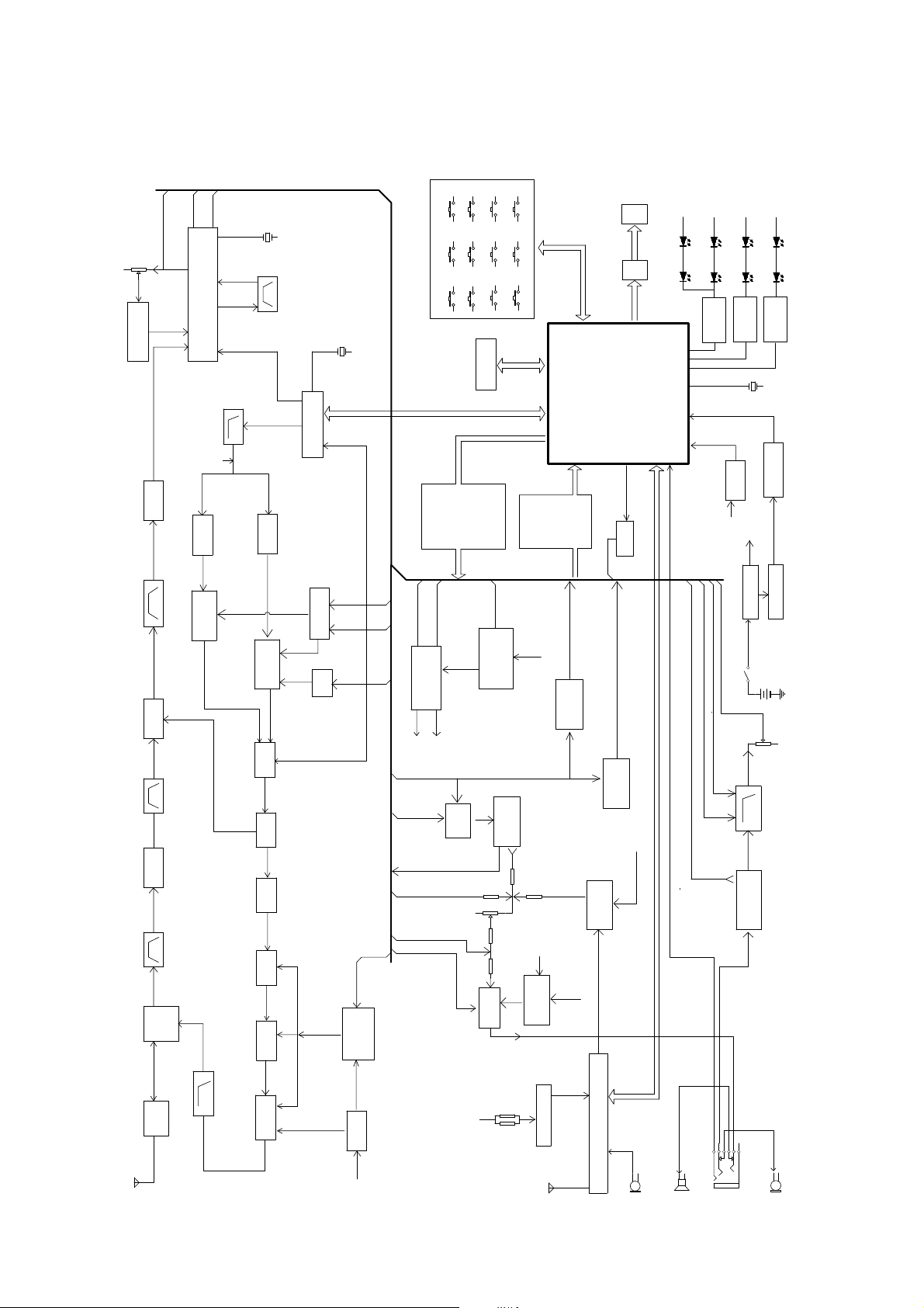
BLOCK DIAGRAM (for HH475)
7
VCC 5V
VCC 5V
B+7.4V
LAMP
RSSI
SQL
AUDIO
SQL
VR1
U1 BA4116
R77
C142
BPF
R90
C141
Q2
IF AMPCRYSTAL BPF
F3,F4
Q8
1st MIX
SAW BPF
156-163MHz
2nd LOCAL MIXER,SQL
2SC4901
D10
F.CONT
HUV307
21.4MHz
Q13
2SK302
RX VCO
3SK318
F2:HDF160B
X1
2nd-IF DET
CBD450C24
BPF
F5 450KHz
2nd-if
20.95MHz
LPF
MOD
PD
D12
F.CONT
HUV307
Q14
TX VCO
2SK210
Q5
2SC4901
BUFFER AMP
D9
DAN235E
RX/TX SW
X2
20.95MHz
CS
U6
PLL
CLK
DATA
KB8825
TX/RX TRANS
Q26:BT3906
Q9:BT3906
D11
HVU307
MOD
LOCK
RX SW
VTX VCO
MOD
PTT
CALL/SQL
TRI
16/9
DOWN
KEY BOARD
UP
DATA BACKUP
CPU PART
APC
RX SW
Q24:BT3906
RX 5V
AUDIO
AF MUTE
AF SW
RX SW
VTX VCO
AF MUTE
V TXPOW
BT_AUDIO SW
V TXPOW
VCC 5V
Q25:BT3906
TX 5V
Q27
BT3904
BT REW
MEM
SCAN
H/M/L
U9
AT4SDBD41B
SQL
CALL/BEEP
WX_ALERT/BURP
SAVE
Q17:Bt3904
D16: BAW56
Q18:S8550
LPF
U5:D
LM324(1/4)
RSSI
CALL DET
AF_REC_IN
MIC_REC_IN
1050Hz&ATIS
B+7.4V
CALL DET
U5:C
CALL DET
LM324(1/4)
LCD
U402
HT1621
LCD DRIVER
U205
PIC24FJ64GA006
PWM OUT
REW/ATIS
U4:D
PWM LPF
LM324(1/4)
ATIS
REW AUDIO
1050HZ&ATIS
U5:A
LM324(1/4)
1050Hz&ATIS DET
D4
D7
D3
LCD BACK LAMP
CLONE
BT_TXD/RXD
D6
KEY BACK LAMP 1
Q28
LED DRIVER
RESET
LOB BAT
LOW BAT
B+7.4V
MOD
CALL
ATIS
MIC_REC_IN
B+7.4V
D7
D19
D6
KEY BACK LAMP 2
LED DRIVER
R149R148
B+7.4V
VR3:B
D17
BT KEY BACK LAMP
Q30
Q29
LED DRIVER
X3
7.3728MHz
U3
RESET
XC61CN2702M
+5V
CPU 3.3V
U8:XC6204B502
U10:XC6204B332
BATTERIES
Li-POLYMER_7.4V
VR2
LPF
U4:C
LM324(1/4)
Q7
2SC4901
RF AMP
Q4
AMP
2SC4901
SAW BPF
156-163MHz
F1:HDF160B
D1,D2
ANT SW
1SS356
Q1
2SC4901
LPF
LPF
L1,L2
C62,C16
C1,C5,C12
ANT
Q3
2SC4901
BUFFER AMP
Q12
2SK3078
TX YOUNGER
Q6
RD07MVS1
TX POWER AMP.
RF PART
APC
U2: LM2904
Q10: MB3904
Q11: MB3904
H/M/L POWER CONTROL
R103R102
R104
CURRENT DET
B+7.4V
AF_REC_IN
REW AUDIOBT_AUDIO
CALL/BEEP
WX_ALERT/BURP
R17
10K
R16
10K
R49
10K
VOL
330
VR3:A
R198
VOL 10K
B+7.4V
10K
R192
U11
AF POWER AMP
B+7.4V
S8550
Q16,Q21,Q22
NJM2070
R138
47
47
R41
U112:XC6204B332
BT_AUDIO SW
Q23
2SC4097
AF SW
BT3904 X 2
BT_AUDIO
BT 3.3V
U13
BLUETOOTH
BLUETOOTH MOEULE TXB206AR
BT_ANT
SPEAKER
BT_MIC
U4:A,B
LM324(2/4)
MIC AMP
13456
2
J2
SP/MIC JACK
VHF_MIC
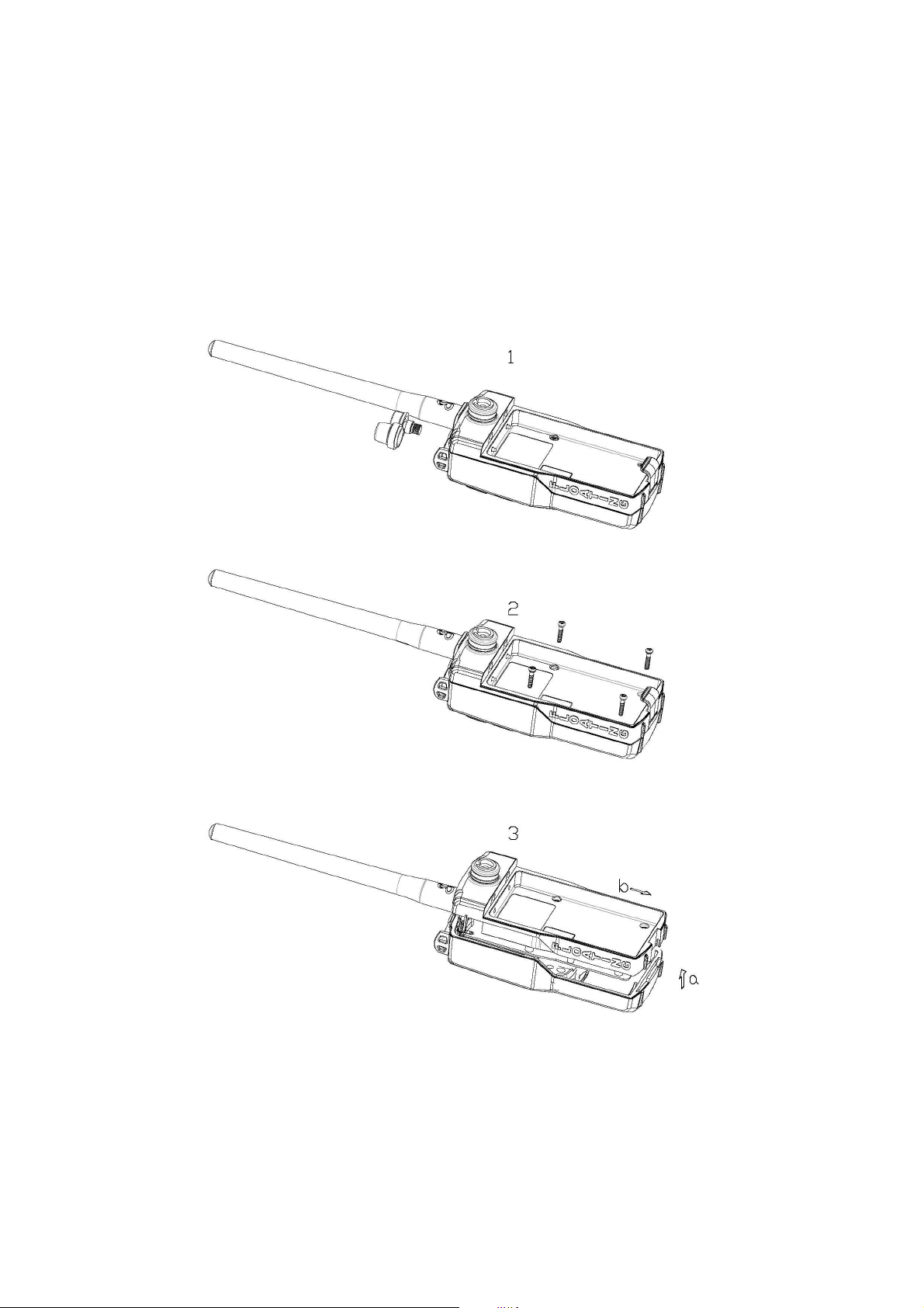
DISASSEMBLY INSTRUCTIONS
8
To remove the front and rear panels from the main chassis:
1. Remove the SPK/MIC and VOL/SQL knob from the main unit.
2. Remove 4 screws from the rear housing for main unit.
3. Detach the rear housing from the front housing.
ALIGNMENT PROCEDURES
METER
COUNTER
METER
9
This transceiver is completely aligned at the factory and does not require any adjustments for installation.
However it is considered as good practice to verify that none of the adjustments have changed.
The test equipment listed below are used for the test setup shown in Fig. 3.1.
This test setup used either partially or totally during the following adjustments.
A.TEST EQUIPMENT
1) DC Power Supply (7.2V DC) 0 - 15V 3A max.
2) RF Power Meter 10 W 50 Ohm 100-200 MHz
3) RF Signal Generator 100-200 MHz, 50 ohm termination
4) FM Linear Detector (FMLD) 100-200 MHz
5) Frequency Counter 1-500 MHz
6) Oscilloscope 20 MHz
7) Distortion Meter
8) SINADDER (Trademark of Helper Instruments Co.)
9) Audio Oscillator
10) Toggle Switch (for use as PTT switch).
Fig. 3.1
AUDIO OSC
PTT
SWITCH
DC POWER
SUPPLY
MIC
UNIT
UNDER TEST
ANT
RX
RY
RF SG
SPEAKER
JACK
COUPLER
RF POWER
OSCILLOSCOPE
SINADDER
FMLD
FREQ
DISTORT

ADJUSTMENT PROCEDURE
10
Step Adjustment Test Point Procedure
1. Connect digital voltmeter to TP1 on RF PCB.
1 L18 Receive *1 TP1
2 L20 Transmit *1 TP1
3 VC1 *2
VR2
4
Modulation *2
2. Set CH01 .
3. Adjust L18.
4. TP1 voltage 1.2~1.6V DC.
1. Connect a digital voltmeter to TP1 on RF PCB.
2. Set CH01 .
3. Adjust L20.
4. TP1 voltage 1.2~1.6V DC.
1. Connect the antenna coupler output to a frequency counter.
2. Set channel to CH01 (156.050 MHz).
3. Adjust VC1 to obtain a frequency reading 156.050 MHz±200Hz.
1. Connect the antenna coupler output to an FM linear detector.
2. Connect Audio Oscillator to Microphone Jack.
3. Set unit to transmit mode.
4. Set audio oscillator output to -23dBm 1 kHz.
5. Adjust VR2 to obtain ±4.5 kHz deviation.
Remark:
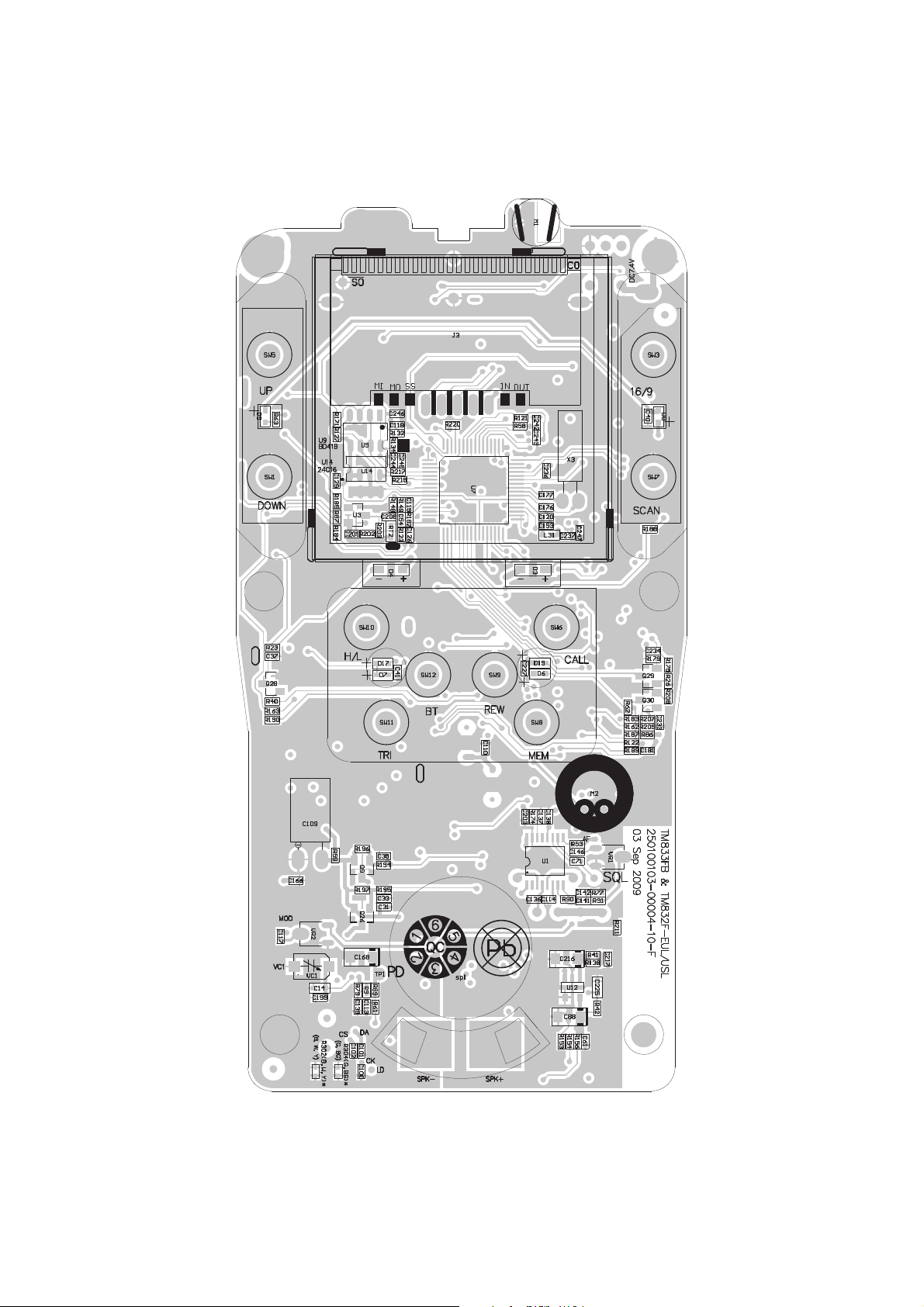
*1: Please reference the “Main PCB Bottom View” drawing in page 13.
*2: Please reference the “Main PCB Top View” drawing in page 12.
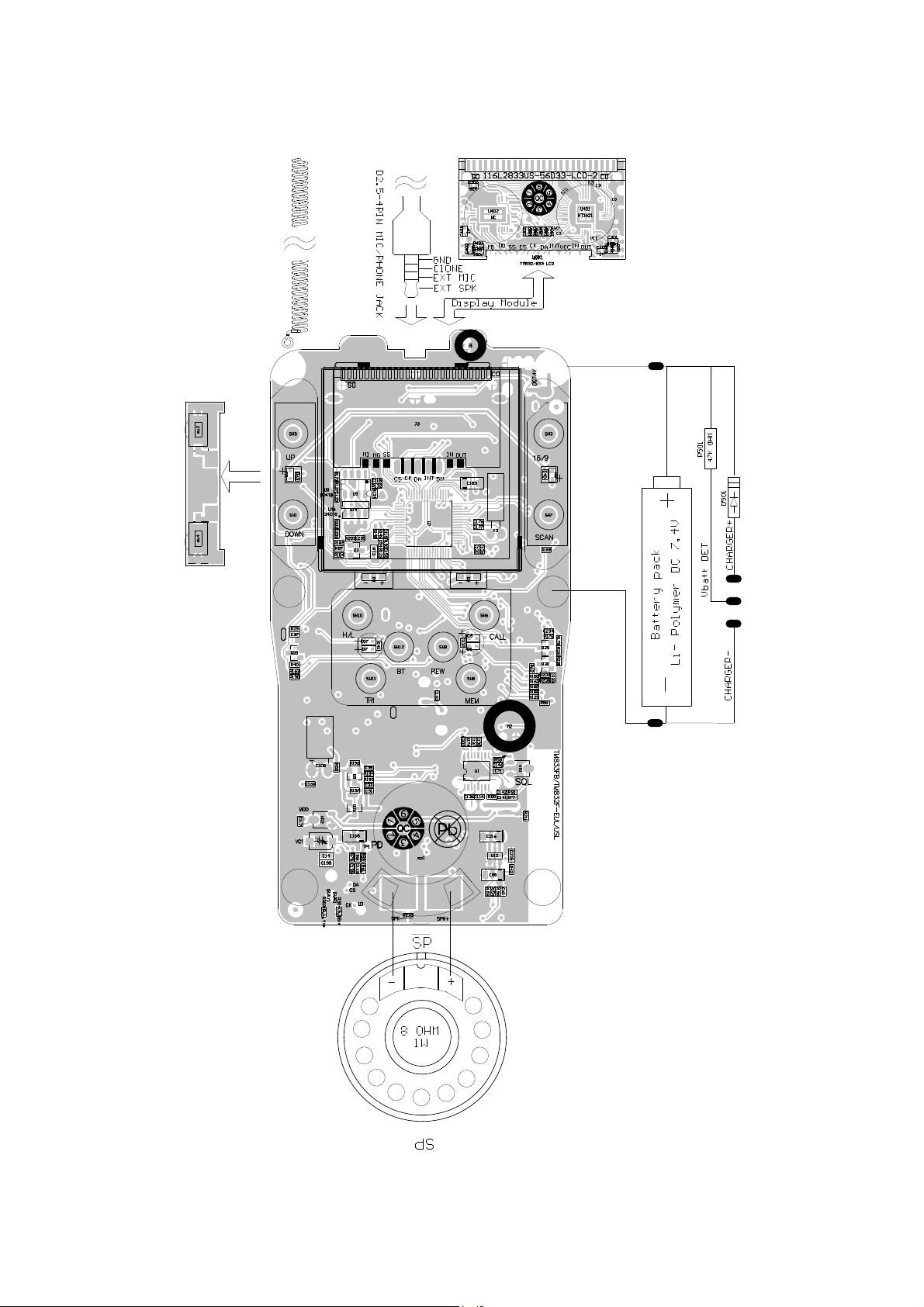
WIRING DIAGRAM
11
MainPCBTopView
12
PRINTEDCIRCUITBOARD
VR2
VC1
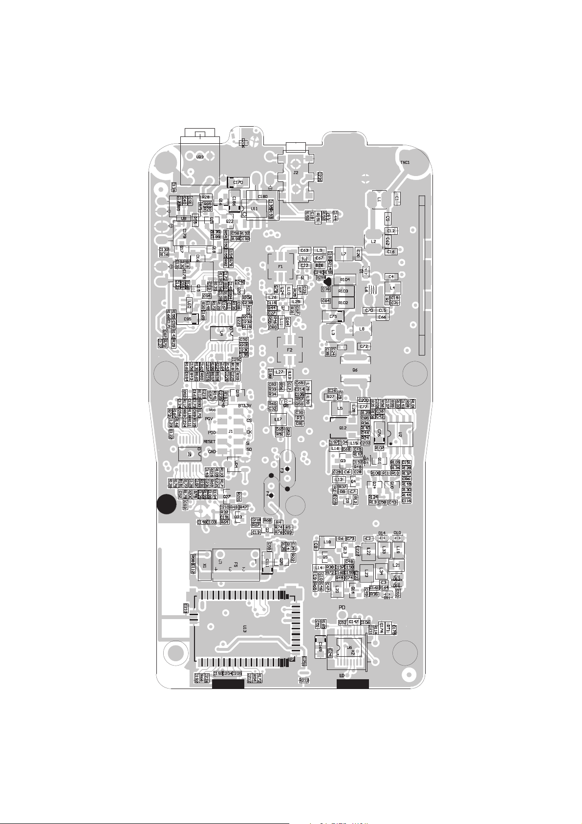
MainPCBBottomView
13
PRINTEDCIRCUITBOARD
L18
L20
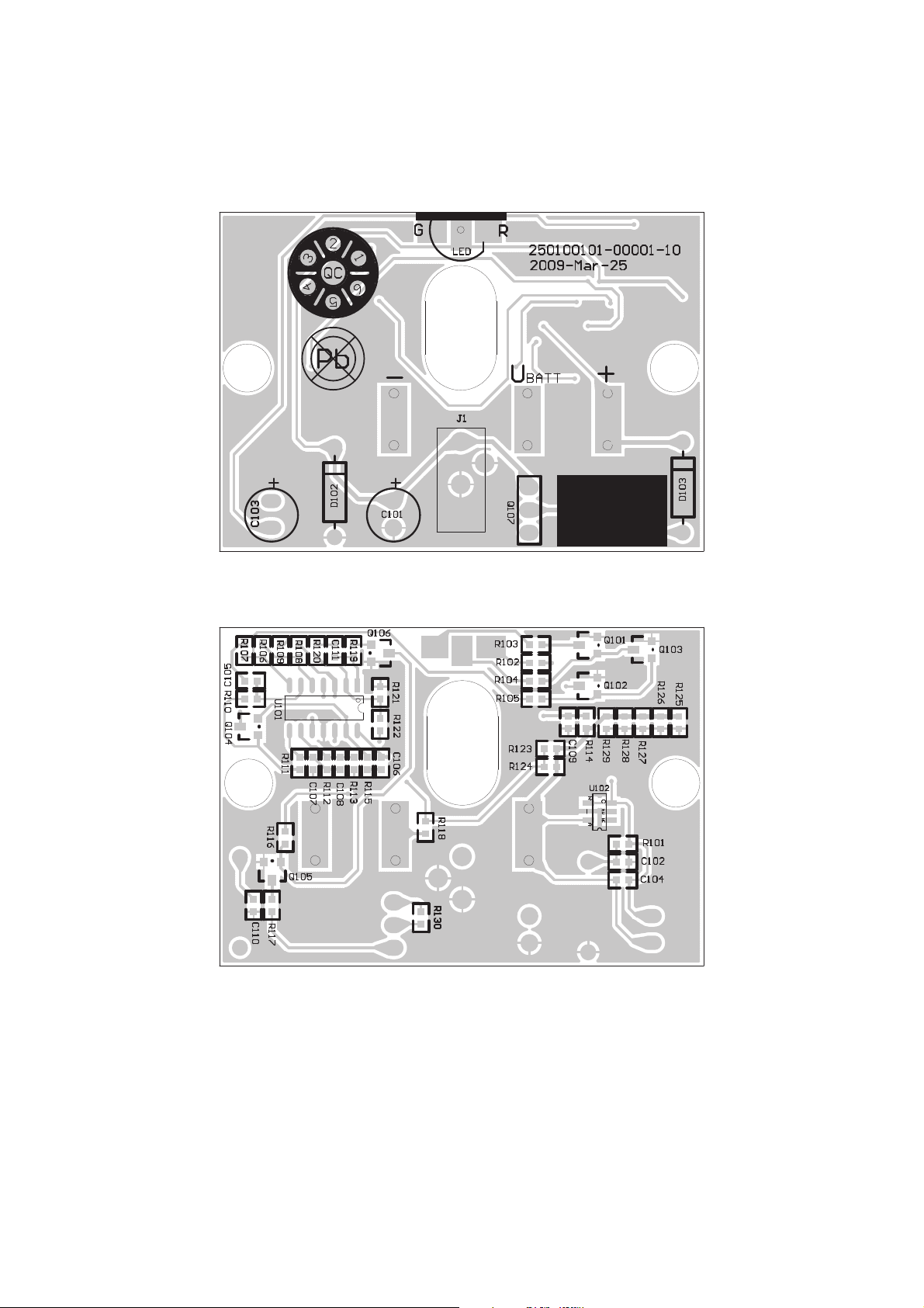
CradleChargerPCBView
14
PRINTEDCIRCUITBOARD
TopView
BottomView

15
TROUBLESHOOTING
Item Symptom Possible Cause
Defective power switch VR3.
1 Unit does not turn on.
Speaker no sound with
2
AF signal applied to
volume control
3 Squelch circuit inoperative
4 No receive (RX)
5 Low receiver sensitivity
6 No transmit (TX)
7 Low RF power output
8 Poor or no modulation
Deviation of transmit
9
frequency
Check the battery voltage.
Defective regulator U8.
Defective volume control.
Defective speaker.
Defective U11 and/or associated components.
Check squelch control.
Defective U1 and/or associated circuitry between pin 9, 10 and
11.
Defective regulator U8.
Check TP1 voltage 0.5 – 4V;
Check second OSC 20.95MHz, pin9 of U6;
Defective Q7, Q8, Q2.
Check U1 audio output voltage at pin 9.
Defective F1 and F2;
Check antenna and connector for possible corrosion or bad
connection.
Failure of the output from Q7, Q8, Q2, U1
Check the output level of local OSC.
Defective PTT switch.
Defective regulator U8.
Check TP1 voltage 0.5 – 4V;
Check power transmits circuit Q12, Q6, D1, D2 and Q1;
Check power control circuit Q17, Q18, Q24;
Check power control circuit U2;
Check RF power output from Q6, If it checks good, then check
and antenna switching diode D1, D2.
If not good then check the voltage level outputs of the drive
amplifiers Q3 and Q12 as well as the associated circuitry.
Defective microphone.
Defective U4 and/or its associated components.
Check crystal X2 and VC1.
EXPLODEDVIEW(forHH475MainPart)
16
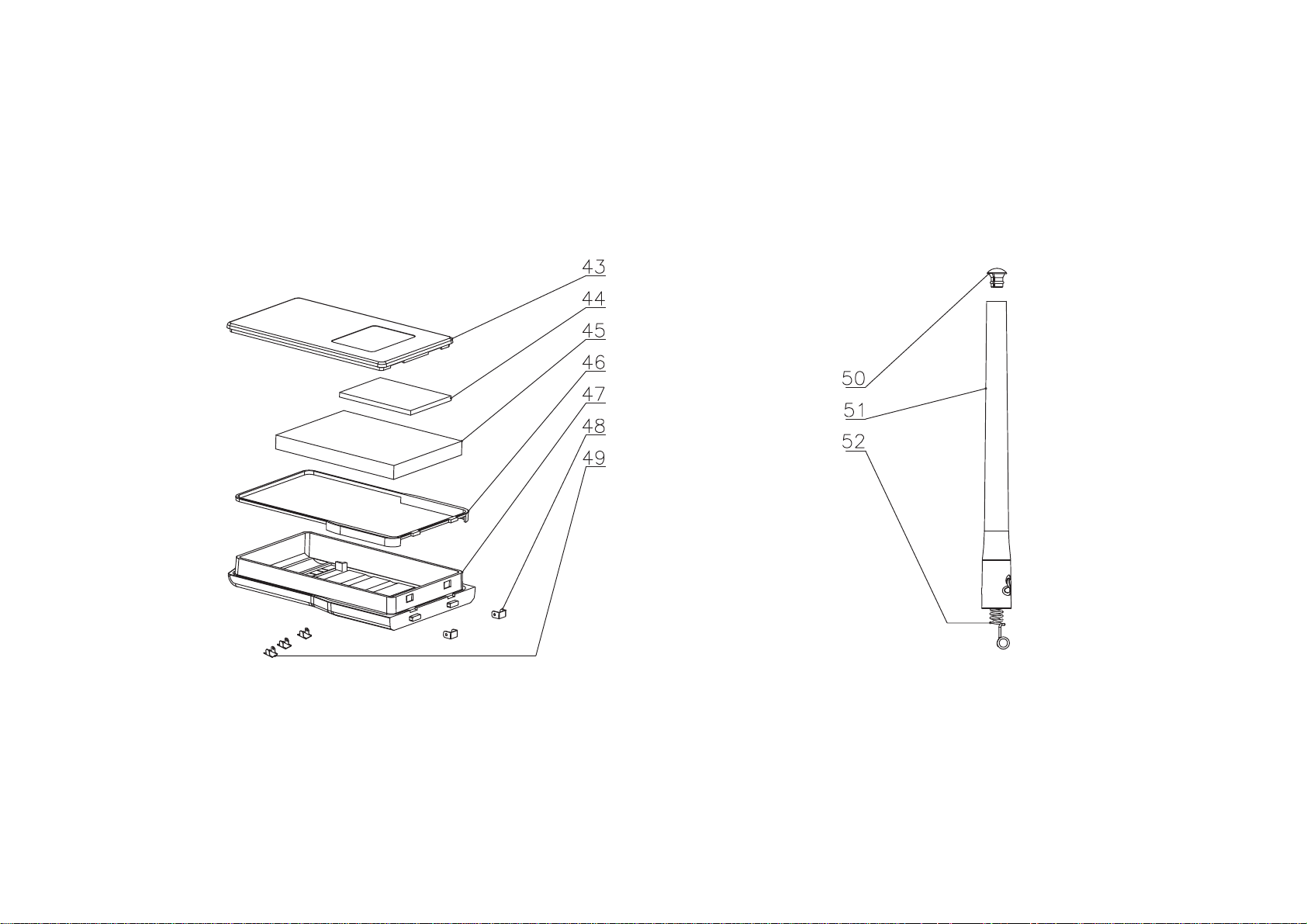
EXPLODEDVIEW(forBatteryand Antenna)
17

Main Radio Part
Location Codes
Description
Mfr's Part No.
EXPLODED VIEW PART LIST
18
1 D-LENS PMMA MU TM833FBUSL 270100034-12003-10
2 P-FCAB MU PC BK TM833FBUSL 3U2X 270100031-12002-10
3 P-KEY VOL MU ABS BK TM833FBUSL 3U2X 270100530-11001-10
4 M-SLEE MU SS L5.15 W5 H4.4 SW 260301122-00001-10
5 P-KEY C/F MU ABS BK TM832EUL MIC 3U2X 270101280-12001-10
6 FOAM-HDR RUBB L34.1W26.3T4.7 GREY DS022 320100108-00001-10
7 INSU-SHET FILM W L-- W-- D6.4 WATERPROOF 270110610-00000-10
8 PCB SS FR4 GP MIC 1-4 L6W8T1.0 TM833FBEU 250102596-00003-10
9 MIC CDR -U -38dB 10V D6.0 T2.7 EM-27PX-5 290100345-00000-10
10 P-PLATE MU PC BK TM832 PTT MOUNT 3U2X 270102092-12001-10
11 KEY-P MAIN RUB DG 6K TM833FBEUL 433C (only for EU) 270200054-11008-10
KEY-P MAIN RUB DG 6K TM833FBUSL 433C (only for US) 270200054-11005-10
12 KEY PTT RUB G 1K TM832 270200131-11001-10
13 KEY FUN SR T 2K TM832FEUL RIGHT 433U/201 (only for EU) 270200016-11004-10
KEY FUN SR T 2K TM832FUSL RIGHT 433U/201 (only for US) 270200016-11003-10
14 KEY FUN SR T 2K TM832FEUL LEFT 433U 270200118-11002-10
15 M-MOUN MU SS L39.3 W37.8 H10.6 LCD 260301094-12001-10
16 LCD TN TSF P 5V 1/4D 1/3B L38.5W37T1.8 - 220100028-00000-10
17 INSU-SHET PVC W L36 W36 D-- ASTIGMATISM 270102604-00001-10
18 D-LENS PMMA MU TM832FEUL Transparent L40 270101425-11002-10
19 SCREW-TS WRH L5 D2 + CZ F RWB (Four) 260100191-00000-10
20 TM833FBEUL /PCBA MAIN/PCBA /R0 COBRA/EU/ 330200008-00000-10
21 M-COVR MU AL L67 W33.2 H6 260300141-11001-10
22 O-RING MU BK RUB H1.4OD--L118.5W62 3U2X 270200053-12001-10
23 M-WASH MU CU NI L10.55 W1.09 H0.2 (Two) 260300005-11001-10
24 SCREW-TS RH L8 D2.6 + SUS C (Two) 260100022-00000-10
25 M-BRKT MU SS L20 W19 H10 SUS304 260302983-11000-10
26 M-SHAF MU PB GD L10.7 W3.6 H-- (Two) 260300007-00001-10
27 P-HOLDER MU ABS BK TM833FBUSL CONNECTOR (Two) 270100532-11001-10
28 P-RCAB MU PC O TM833FBUSL 021U 270100529-11001-10
29 P-CLIP BU PC BK TM832/TM833 ATTACHMENT 3 270102095-12001-10
30 SCREW-TS RH L10 D3 + BZ SUS F BLACK 260101177-00000-10
31 SCREW-TS PH L12 D-- + BZ SUS F TM832FEUL(Four) 260101179-00001-10
32 FOAM-HDR RUBB D1.8T1 NA Black SCREW CAP (Five) 320100751-00001-10
33 M-SPPT MU SS L20 W1 H1 LOCK PIN 260301096-00001-10
34 P-COVER MU PC BK TM832EUL 3U2X/WITH PAIN 270100455-12002-10
35 M-SHIE MU TP NI L20.4 W14.1 H8.5 VCO 260301003-00001-10
36 INSU-SHET PVC W L35.4 W33.4 D0.1 TM832FE 270110041-00001-10
37 INSU-SHET PAP S L40 W1.3 D0.1 TM832FEUL (Three) 270110039-00001-10
38 P-PLATE MU PMMA BK TM832/TM833 KEYBOARD 270102091-12001-10
39 SPK M 8OHM 1W D40 T5.2 TEK404P-8 OHM1W 290100070-00000-10
40 FOAM-SPK NYL D37.3T-- SS BLACK TM833FBEU 320101847-00001-10
41 INSU-TAPE FILM BK L-- W-- D9.4 WATERPROO 270110368-00000-10
42 FOAM-CUH SPNG D9.5T1.4 SS BLACK TM833FBE 320101869-00001-10

Battery Part
Location Codes
Description
Mfr's Part No.
Antenna Part
Location Codes
Description
Mfr's Part No.
EXPLODED VIEW PART LIST - CONTINUED
19
43 P-BATT-DR BU ABS BK TM832EUL 3U2X 270101071-12001-10
44 FOAM-HDR SPNG L40W8T1 Black (Two) 320100666-00001-10
45 BAT-R PRISM LI 7.4V 1000MAH TP603450 TEC 230400180-00000-10
46 O-RING BD BK RUB H5.4OD--L94.05W59 270200380-13001-10
47 P-RCAB BT ABS BK TM833 3U 2X 270100953-11001-10
48 CON-COMM PB T0.2H5WD-- GD C (Two) 260300377-11001-10
49 CON-CHAR PB T0.2H3.5WD-- GD UNIT (Three) 260300380-11001-10
50 P-CAP BU ABS BK TM833/832 ANT 3U2X 270102110-11001-10
51 P-SLV-ANT BU PU BK TM832EUL ANT 3U2X 270102093-12001-10
52 SPRING COS ANT SW CU WD1 L158.5 OD:6.8MM 260200009-00000-10

Location Codes
Description
Mfr's Part No.
TM833FBEUL /U- U-M /R0 COBRA/EU
330100058-00000-10
TM833FBEUL /U- MAIN/UNIT /R0 COBRA/EU
330100062-00000-10
TM833USL /E&M ALK BATT COMP /R0 COBRA-US
330503423-00000-10
20
TM833FBEUL /PCBA MAIN/PCBA /R0 COBRA/EU/
330200008-00000-10
TM833FBEUL /PCBA MAIN/SOLDERING/PCBA /R0
330201917-00000-10
TM832EUL /COBA LCD BONDING PCBA /R0 COBR
330301732-00000-10
TM832EUL /SMTA LCD PCBA /R0 COBRA-EUR
330401965-00000-10
Alkaline Battery Assembly
20
SPRING COS GD WD0.6 L31.2 260200065-00000-10
SPRING COS GD WD0.6 L22.1(Two) 260200066-00000-10
SPRING COS GD WD0.6 L22.1(Two) 260200067-00000-10
SPRING COS GD WD0.6 L23.3 260200068-00000-10
CON-POST PB T0.2H14.1WD-- GD BATT B 260300376-11001-10
CON-COMM PB T0.2H75.3WD-- GD A 260300379-12001-10
P-RCAB BT ABS BK TM833USL 3U 2X 270100527-13001-10
INSU-SHET FIBER BK L75.3 W3.9 D-- 0.15 270102608-00001-10
O-RING BD BK RUB H5.4OD--L94.05W59 270200380-13001-10
Main PCB Assembly
16 LCD TN TSF P 5V 1/4D 1/3B L38.5W37T1.8 - 220100028-00000-10
RUBCON SRI PIT0.10 L30.1 W2.0 H5.2 240300313-00000-10
21 M-COVR MU AL L67 W33.2 H6 260300141-11001-10
35 M-SHIE MU TP NI L20.4 W14.1 H8.5 VCO 260301003-00001-10
15 M-MOUN MU SS L39.3 W37.8 H10.6 LCD 260301094-12001-10
SHIELD VCOC MS NI L21.7 W14.7 T3.8 SILVE 260302892-11001-10
18 D-LENS PMMA MU TM832FEUL Transparent L40 270101425-11002-10
17 INSU-SHET PVC W L36 W36 D-- ASTIGMATISM 270102604-00001-10
INLAY MKEY PVC L34 W22 TM832/TM833 UNIT 270102692-11001-10
INLAY MKEY PET L25.4 W7.6 TM832/833 (Two) 270102693-11001-10
37 INSU-SHET PAP S L40 W1.3 D0.1 TM832FEUL (Three) 270110039-00001-10
36 INSU-SHET PVC W L35.4 W33.4 D0.1 TM832FE 270110041-00001-10
FOAM-CUH SILI L12W6.5T3 GREY 320100009-00001-10
FOAM-HDR SPNG L40W4T3 Grey (Four) 320100664-00001-10
FOAM-CUH SPNG L9W7T1 White 320100696-00000-10
FOAM-SPON SPNG L33.4W3.0T2.0 BLACK TM832 320101829-00001-10
PARTS LIST (HH475 Eu)
C109 CAP-RELE 100 uF M 10V D5 H8 280201079-00000-10
C178 CAP-RELE 100 uF M 10V D5 H8 280201079-00000-10
C179 CAP-RELE 100 uF M 10V D5 H8 280201079-00000-10
C180 CAP-RELE 100 uF M 16V D6 H5 280201082-00000-10
C185 CAP-RELE 10 uF M 25V D4 H5 280201073-00000-10
F3 XTL 21.4M 2.5 2pF L3.2 W8 H6 -20C ~ 70C 280700099-00000-10
F4 XTL 21.4M 2.5 2pF L3.2 W8 H6 -20C ~ 70C 280700099-00000-10
F5 FLTR-REC LEAD 450 K +/-7.5 KHz@ 6dB LTM4 280700243-00000-10
U13 RF-MOD BLUETOOTH TXB-206AR 2.4GHZ TXBANG 320200029-00000-10
VR3 VR-ST LOG 10 Kohm P DIP H R A;JIS;W/S 280101743-00000-10
X1 FLTR-REC LEAD 450 K +/-4 KHz@ 3dB CDB450 280700253-00000-10
X2 XTL 20.95M 2.5 15pF L8 W7.8 H3 -30C ~ 50 280700161-00000-10
X3 XTL 7.3728 M 30 12.5pF D3.0 H8.0 -10+60 280700031-00000-10
MIC CDR -O -52dB 3V D9.7 T4.5 LYS-M9745- 290100001-00000-10
U401 A-IC ANA HT1621(DICE-SD1706) CHIP 48 BON 210100060-00000-10
PCB DS FR4 GP LCD3 L32W20T1 250100356-00003-10
C401 CAP-CCER 100 nF K 16 VDC 0402 X7R 280200343-00000-10
C407 CAP-CCER 100 nF K 16 VDC 0402 X7R 280200343-00000-10

Location Codes
Description
Mfr's Part No.
TM832EUL /SMTA PTT PCBA /R0 COBRA-EUR
330401964-00000-10
TM833FBEUL /SMTA MAIN/TOP/SMD/PCBA /R0 C
330401411-00000-10
PARTS LIST (HH475 Eu) - CONTINUED
21
Main PCB Assembly
C409 CAP-CCER 1000 pF K 50 VDC 0402 X7R 1570- 280200327-00000-10
R401 RES TFC 4.7 Kohm 0402 J 1/16W 280101287-00000-10
R402 RES TFC 100 ohm 0402 J 1/16W 280100919-00000-10
SW-TACT SMD V 12V 5mA TSUY-2SL 1P2T HUA (Two) 240400313-00000-10
PCB DS FR4 GP PTT2 L33W8T1 250100355-00002-10
C14 CAP-CCER 27 pF J 50 VDC 0603 COG 280200800-00000-10
C31 CAP-CCER 1000 pF K 50 VDC 0402 X7R 1570- 280200327-00000-10
C33 CAP-CCER 1000 pF K 50 VDC 0402 X7R 1570- 280200327-00000-10
C35 CAP-CCER 1000 pF K 50 VDC 0402 X7R 1570- 280200327-00000-10
C37 CAP-CCER 1000 pF K 50 VDC 0402 X7R 1570- 280200327-00000-10
C40 CAP-CCER 1000 pF K 50 VDC 0402 X7R 1570- 280200327-00000-10
C41 CAP-CCER 1000 pF K 50 VDC 0402 X7R 1570- 280200327-00000-10
C54 CAP-CCER 1000 pF K 50 VDC 0402 X7R 1570- 280200327-00000-10
C61 CAP-CCER 100 nF K 16 VDC 0402 X7R 280200343-00000-10
C71 CAP-CCER 56 pF J 50 VDC 0402 COG 280200859-00000-10
C88 CAP-CTAN 22 uF M 10 VDC CASEA 280201245-00000-10
C100 CAP-CCER 470 pF J 50 VDC 0402 COG 280200840-00000-10
C101 CAP-CCER 470 pF J 50 VDC 0402 COG 280200840-00000-10
C102 CAP-CCER 470 pF J 50 VDC 0402 COG 280200840-00000-10
C110 CAP-CCER 2 pF C 50 VDC 0402 COG 280200779-00000-10
C113 CAP-CCER 100 nF K 16 VDC 0402 X7R 280200343-00000-10
C114 CAP-CCER 100 nF K 16 VDC 0402 X7R 280200343-00000-10
C117 CAP-CCER 100 nF K 16 VDC 0402 X7R 280200343-00000-10
C118 CAP-CCER 100 nF K 16 VDC 0402 X7R 280200343-00000-10
C119 CAP-CCER 100 nF K 16 VDC 0402 X7R 280200343-00000-10
C120 CAP-CCER 100 nF K 16 VDC 0402 X7R 280200343-00000-10
C126 CAP-CCER 100 nF K 16 VDC 0402 X7R 280200343-00000-10
C129 CAP-CCER 100 nF K 16 VDC 0402 X7R 280200343-00000-10
C136 CAP-CCER 220 nF Z 16 VDC 0402 Y5V 280200303-00000-10
C137 CAP-CCER 33 nF K 16 VDC 0402 X7R 280200428-00000-10
C138 CAP-CCER 33 nF K 16 VDC 0402 X7R 280200428-00000-10
C139 CAP-CCER 33 nF K 16 VDC 0402 X7R 280200428-00000-10
C141 CAP-CCER 220 pF J 50 VDC 0402 COG 280200786-00000-10
C142 CAP-CCER 220 pF J 50 VDC 0402 COG 280200786-00000-10
C146 CAP-CCER 820 pF J 50 VDC 0402 COG 280200888-00000-10
C153 CAP-CCER 1000 pF K 50 VDC 0402 X7R 1570- 280200327-00000-10
C166 CAP-CCER 47 nF K 25 VDC 0402 X7R 280200453-00000-10
C168 CAP-CTAN 2.2 uF M 16 VDC CASEA 280201248-00000-10
C176 CAP-CCER 10 pF J 50 VDC 0402 NPO 1570-03 280200583-00000-10
C177 CAP-CCER 10 pF J 50 VDC 0402 NPO 1570-03 280200583-00000-10
C181 CAP-CCER 1 uF Z 6.3 VDC 0402 Y5V 280200290-00000-10
C199 CAP-CCER 3 pF C 50 VDC 0402 COG 280200811-00000-10
C203 CAP-CCER 1000 pF K 50 VDC 0402 X7R 1570- 280200327-00000-10
C208 CAP-CCER 100 nF K 16 VDC 0402 X7R 280200343-00000-10
C209 CAP-CCER 100 nF K 16 VDC 0402 X7R 280200343-00000-10
C216 CAP-CTAN 22 uF M 10 VDC CASEA 280201245-00000-10
C217 CAP-CCER 100 nF K 16 VDC 0402 X7R 280200343-00000-10
C225 CAP-CCER 1 uF Z 10 VDC 0603 Y5V 280200293-00000-10
C227 CAP-CCER 1000 pF K 50 VDC 0402 X7R 1570- 280200327-00000-10
 Loading...