

Page 1

MARINE HANDHELD TRANSCEIVER
Catalog Number: MR HH330 FLT /EU
CONTENTS
MR HH330 FLT /EU
Page
Specifications........................................................................................................................................................2
Theory of Operation...............................................................................................................................................4
Block Diagram.......................................................................................................................................................6
Disassembly Instructions................................................................... ..................................................................7
Alignment Procedures...........................................................................................................................................8
Adjustment Procedure...........................................................................................................................................9
Wiring Diagram....................................................................................................................................................10
Printed Circuit Board............................................................................................................................................11
Troubleshooting..................................................................................................................................................15
Exploded View.....................................................................................................................................................15
Exploded View Part List......................................................................................................................................17
Electrical &Packing &Other Parts List..................................................................................................................19
IC Lead Identification and Internal Diagram.........................................................................................................49
Transistor Lead Identification...............................................................................................................................58
VoltageChart.......................................................................................................................................................59
Schematic Diagram.............................................................................................................................................63
Version:01 Date: Apr 02, 2010
Page 2

SPECIFICATIONS
DESCRIPTION Unit LIMIT
Frequency Range: Transmit MHz 156.025 To 157.425.
Frequency Range: Receive MHz 156.050 To 162.025 (Eu)
156.050 To 163.275 (Us)
Number Of Channels 59 INT, 57 USA, 57 Canada
10 Weather Channels (only for Us)
100 Memory Channels
Oscillate Mode PLL
Modulation FM(16K0G3E)
Channel Spacing KHz 25
Frequency Stability PPM ±10
Standard Operation Temperature °C -15 To+55 (Eu), -20 To+50 (Us)
Normal Working Voltage V 7.4
Low Limit Working Voltage V 7.35
Battery Lifetime (Tx 5% / Rx 5% / Standby 90%) Hour 8 ( 6W @ 7.4V / 1000mAH )
16 ( 1W @ 7.4V / 1000mAH )
Memory Resented EEPROM
Antenna Socket FIXED
Display LCD With Background Light
Built-ln Speaker Diameter 40mm / Impedance 8 Ohm
VHF RECEIVER Unit LIMIT
Sensitivity For 12dB Sinad uV 0.30
20dB Quieting uV 0.35
Rated audio output@5% Thd Speaker mW ≥ 250
Deviation sens. For rated output (VR @ max.) ±kHz ≤ 2.5
Max. S/N ratio @ 1mV dB ≥ 40
Audio frequency resp.
@300HZ dB 9 ± 3
@2500HZ dB -9 ± 3
Speaker output 8Ω load @ Max Vol mW ≥ 400
Standby Current mA ≤ 50 (Eu), 68 (Us)
Receiver Current @ Max Vol. mA ≤ 200
Charging current mA 180 ± 30
2
Page 3

Weather RECEIVER (only for US) Unit LIMIT
Sensitivity For 12dB Sinad dBm ≤ -100
Sensitivity For WX Alarm (1050Hz Dev.3KHz) dBm ≤ -100
TRANSMITTER Unit LIMIT
Carrier power(no mod)
Hi W 6±0.8
Med W 3±0.5
Lo W 0.8±0.2
Carrier freq. Tolerance ppm ± 10
Modulation limiting ±kHz 4.3~ 4.9
Audio frequency response
@300HZ dB
-12 ± 3
@2500HZ dB +7 ± 3
Audio distortion @ 2.5 kHz dew.) % ≤ 5
Hum and noise ratio dB 40
Mic sens. for 3 kHz mV 7±3
Current drain
Transmit(High) A ≤ 2.0
Transmit(Med) A ≤ 1.5
Transmit(Low) A ≤ 0.9
Mic Modulation Sen. ( at Sound level of 94 dBA ) ±kHz ≥ 1.5
Mic Modulation Limiting ( at Sound level of 110 dBA ) ±kHz 4.0 ~ 4.9
Note: Nominal specifications represent the design specifications. All units should be able to approximate these
specs. Some will exceed these specs, and others may drop slightly below them. Limit specs represent the
absolute worst condition that might still be considered acceptable. A unit should never fail to meet limit specs.
3
Page 4

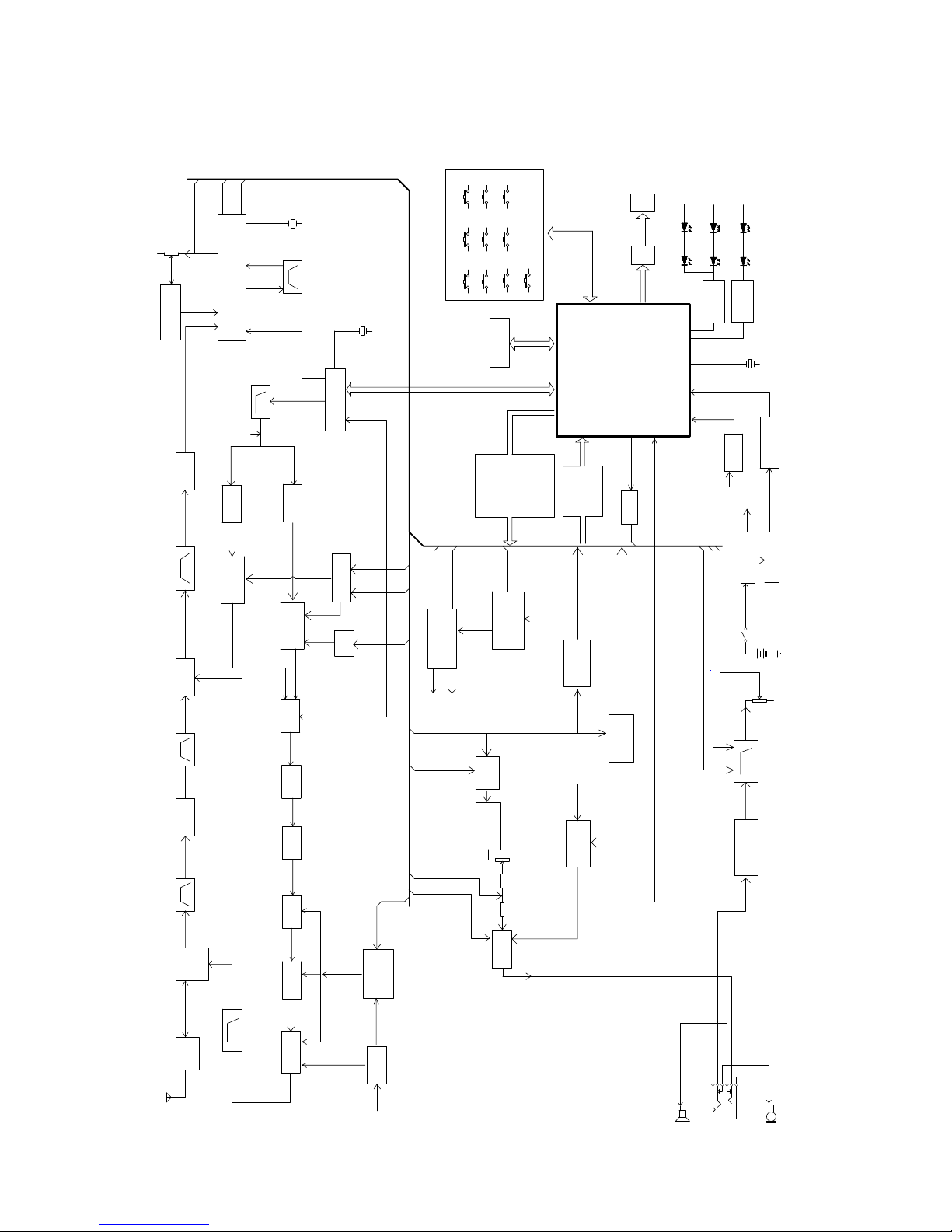
THEORY OF OPERATION
This PLL - controlled VHF marine transceiver provides an accurate and stable multi-channel operation.
The transceiver consists of 6 main sections:
z Transmitter
z Receiver
z Low voltage detection
z Local oscillator PLL (Phase Lock Loop) Circuit
z Memory backup
z ATIS(Automatic Transmitter Identification System)
z Transmitter
The audio is picked up from the internal MIC, the audio signal is then amplified by Audio Amplifier, U4
LM324 (2/4), U4 (3/4) and filtered by a low pass filter U4 (4/4). The audio is adjusted with VR2 to
obtain a suitable Audio frequency response, and then modulated with the carrier by VCO, through
Varicap (D11).
The modulated signal output from the VCO is pre-amplified by Q5, Q4 and Q3. Then it is amplified by
Q12, Q6 .The amplified signal then passes through a low -pass filter network which consists of C72,
L8, C66, C15, L6, C4 filters out spurious emission, and the antenna switching circuit, D1, D2. The
signal is filtered by another low-pass filter circuit which consists of C16, L2, C62, C12, L1, C5, C1.
These low pass filters are necessary to suppress the second and third harmonics. The signal is then
fed into the antenna input and radiated out.
TX current is converted into a voltage signal, that signal fed into U2 LM2904 (2/2) for sampling. U2 is
the Automatic power control (APC) circuit.
When the unit is transmitting, the audio signal is added to the TX VCO Varicap D11. The capacitance
of D11 is varied following the audio signal and when mixed with the carrier to form the modulated
signal.
z Receiver
The receiver uses a double frequency super-heterodyne circuit. The first Immediate Frequency (IF) is
21.4 MHz and the second is 450 kHz.
The RF signal is received by the antenna, and passes through a low-pass filter network C1, L1, C5,
C12, L2, C62, C16, C20, L7, C67 to filter out the unwanted signals, the antenna switching circuit D1,
D2 switching circuit to receive. The received RF signal is sent to a SAW filter F1 to filter out-of-band
signals. The RF amplifier Q7 amplifies signals within the range of the frequency coverage and passes
though another saw filter F2 to further filter out-of-band signals. The RF signal then is mixed with the
local oscillation frequency by the mixer Q8. A first IF (Immediate Frequency) 21.4 MHz is produced.
The IF is passed through a pair of crystal filter F3 (1/2), F4 (2/2) to further filter other unwanted
signals. The first IF then is amplified by Q2 and the IF amplifier U1 (BA4116). U1 is a integrated RF
amplifier which consists of a local oscillator, a demodulator, a second mixer, squelch control circuit,
4
Page 5

and RF amplifier. The 21.4 MHz IF then is mixed here with second mixer and converted into 2nd
Immediate Frequency (IF) 450 kHz. The 2nd IF passes through a ceramic filter F5 to filter out the
residue unwanted signal at pin 5 of U1 (BA4116) output this final IF signal and the Audio signal is
output at pin 9 of U1 (BA4116).
The audio signal is fed through a volume control VR3 and finally amplified by Audio amplifier U11
(NJM2070) and heard in the speaker.
The squelch control is also controlled by U1 (BA4116). The second IF passes through U1 (BA4116)
internal squelch control R90, C141, C142 form as a squelch amplifier. The ceramic filter produces a
squelch signal (RF noise). Pin 14 of U1 sends the digital squelch control signal to the CPU mute the
audio speaker path. Pin 12 of U1 output a RSSI level to the CPU.
z Low Voltage Detection
The battery voltage, divided by R148, R149 is input to U7 Pin 11 for voltage level sample.
z PLL (Phase Lock Loop) Circuit:
The receiver and transmitter both share the same PLL (Phase Lock Loop) Circuit to produce the
carrier or the receive frequency. The local oscillator consists of a fundamental frequency oscillator X2
20.95MHz and U6 (GP214D). A phase Lock Loop (PLL) U6 (KB8825), TX VCO Q14 and RX VCO
Q13. The fundamental frequency is frequency divided by U6 and a 12.5 kHz signal is produced.
When the VCO frequency applied to and frequency divided by U6 produces a frequency comparable
to 12.5 kHz, PLL will control the VCO. When these two frequencies are matched, a constant control
voltage is output from PLL to lock VCO in desired frequency. The PLL also will output a lock
indication to MCU to indicate the PLL is in frequency lock state.
z Memory Backup
U14 is an EEPROM AT24C16 which acts as a memory backup for the working channel code and the
system parameters. Every time when the unit is switched on, the MCU will reset the system, clear
the RAM, and recall in the memory from the EEPROM to refresh the RAM in CPU U7.
z ATIS(Automatic Transmitter Identification System) only for EU
ATIS circuit consists of U5(1/4),U4(4/4) and CPU U7, when receiving the AF signal from U1 Pin 9 via
U5(1/4) then pass to CPU U7 Pin 43, when transmitting AITS PWM signal form U7 Pin 45 output then
via U4(4/4) pass to TX VCO Varicap D11 then mixes with the carrier to form the modulated signal.
5
Page 6
D3
X2
20.95MHz
SPEAKER
MIC
X3
7.3728MHz
VR3:C
VR2
MOD
U2: LM2904
APC
R103R102
CURRENT DET
U5:A
1SS356
21.4MHz
LOB BAT
DAN235E
D9
2SC4901
Q26:BT3906
2SC4901
3SK318
2SC4901
R149R148
TX POWER AMP.
F3,F4
LOW BAT
Q5
BUFFER AMP
RX/TX SW
2SC4901
Q3
BUFFER AMP
2SK3078
Q12
TX YOUNGER
U1 BA4116
2nd LOCAL MIXER,SQL
Q2
IF AMPCRYSTAL BPF
Q8
1st MIX
Q7
RF AMP
D1,D2
ANT SW
TX/RX TRANS
ANT
Q9:BT3906
VTX VCO
U6
AUDIO
AF POWER
AF POWER AMP
Q16,Q21,Q22
S8550
U11
BT3904 X 2
MIC AMP
NJM2070
U4:A,B
LM324(2/4)
LM324(1/4)
AF MUTE
U205
PIC24FJ64GA006
DATA BACKUP
U14
24C16
U8:XC6204B502
Q18:S8550
AUDIO
Q6
RD07MVS1
LCD
BPF
R77
C141
C142
KB8825
PLL
U4:C
ATIS
F5 450KHz
2nd-if
RX VCO
Q13
2nd-IF DET
H/M/L POWER CONTROL
R90
TX VCO
Q14
2SC4901
Q4
AMP
2SK210
2SK302
D11
MOD
1050Hz&ATIS DET
U3
RESET
XC61CN2702M
RESET
Q17:Bt3904
D16: BAW56
LM324(1/4)
LPF
BPF
LPF
LPF
SAW BPF
HVU307
MOD
HUV307
D10
HUV307
D12
F.CONT
F.CONT
F1:HDF160B
RSSI
SQL
SQL
SQL
RSSI
B+7.4V
B+7.4V
B+7.4V
B+7.4V
CALL/BEEP
AF SW
1050HZ&ATIS
1050Hz&ATIS
AF SW
AF MUTE
RX SW
VTX VCO
RX SW
TX 5V
RX 5V
RX SW
V TXPOW
VCC 5V
CALL/BEEP
APC
LPF
SAVE
Q10: MB3904
VR1
Q11: MB3904
CLONE
156-163MHz
SAW BPF
156-163MHz
F2:HDF160B
ATIS
X1
CBD450C24
LOCK
U5:D
DATA
LM324(1/4)
CLK
CS
LPF
D4
LCD BACK LAMP
RF PART
CPU PART
BATTERIES
Li-POLYMER_7.4V
13456
2
J2
SP/MIC JACK
Q1
2SC4901
C1,C5,C12
L1,L2
C62,C16
20.95MHz
PD
R104
Q24:BT3906
Q25:BT3906
VCC 5V
U402
HT1621
V TXPOW
MOD
B+7.4V
D6
D7
KEY BACK LAMP 1
VCC 5V
CPU 3.3V
LCD DRIVER
Q27
BT3904
U5:C
CALL DET
LM324(1/4)
CALL DET
CALL DET
CALL
Q28
LED DRIVER
+5V
U10:XC6204B332
Q30
LED DRIVER
D6
D7
KEY BACK LAMP 2
B+7.4V
PWM LPF
ATIS PWM OUT
U4:D
LM324(1/4)
16/9
H/M/L
DOWN
UP
KEY BOARD
TRI
SCAN
LAMP
PTT
CALL/SQL
MEM
VOL
VOL 10K
VR3:A
R198
330
R192
10K
WX_ALERT/BURP
WX_ALERT/BURP
BLOCK DIAGRAM (for HH330)
6
Page 7
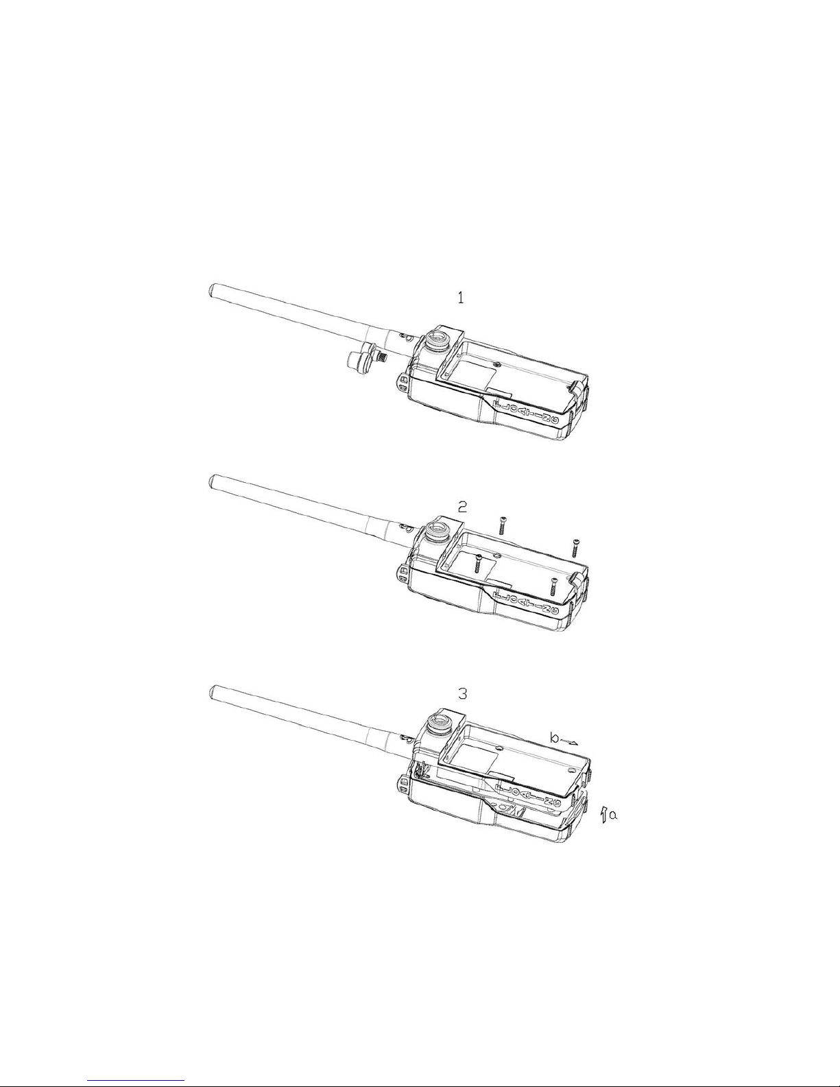
DISASSEMBLY INSTRUCTIONS
To remove the front and rear panels from the main chassis:
1. Remove the SPK/MIC and VOL/SQL knob from the main unit.
2. Remove 4 screws from the rear housing for main unit.
3. Detach the rear housing from the front housing.
7
Page 8
ALIGNMENT AND ADJUSTMENT
This transceiver is completely aligned at the factory and does not require any adjustments for installation.
However it is considered as good practice to verify that none of the adjustments have changed.
The test equipment listed below are used for the test setup shown in Fig. 3.1.
This test setup used either partially or totally during the following adjustments.
A.TEST EQUIPMENT
1) DC Power Supply (7.2V DC) 0 - 15V 3A max.
2) RF Power Meter 10 W 50 Ohm 100-200 MHz
3) RF Signal Generator 100-200 MHz, 50 ohm termination
4) FM Linear Detector (FMLD) 100-200 MHz
5) Frequency Counter 1-500 MHz
6) Oscilloscope 20 MHz
7) Distortion Meter
8) SINADDER (Trademark of Helper Instruments Co.)
9) Audio Oscillator
10) Toggle Switch (for use as PTT switch).
Fig. 3.1
RF POWER
METER
DC POWER
SUPPLY
AUDIO OSC
PTT
SWITCH
UNIT
UNDER TEST
OSCILLOSCOPE
SINADDER
FMLD
FREQ
COUNTER
DISTORT
METER
RF SG
SPEAKER
JACK
MIC
ANT
RX
RY
COUPLER
8
Page 9

ADJUSTMENT PROCEDURE
Step Adjustment Test Point Procedure
1 L18 Receive *1 TP1
1. Connect digital voltmeter to TP1 on RF PCB.
2. Set CH01 .
3. Adjust L18.
4. TP1 voltage 1.2~1.6V DC.
2 L20 Transmit *1 TP1
1. Connect a digital voltmeter to TP1 on RF PCB.
2. Set CH01 .
3. Adjust L20.
4. TP1 voltage 1.2~1.6V DC.
3 VC1 *2
1. Connect the antenna coupler output to a frequency counter.
2. Set channel to CH01 (156.050 MHz).
3. Adjust VC1 to obtain a frequency reading 156.050
MHz±200Hz.
4
VR2
*2
Modulation
1. Connect the antenna coupler output to an FM linear detector.
2. Connect Audio Oscillator to Microphone Jack.
3. Set unit to transmit mode.
4. Set audio oscillator output to -23dBm 1 kHz.
5. Adjust VR2 to obtain ±4.5 kHz deviation.
Remark:
*1: Please reference the “Main PCB Bottom View” drawing in page 12.
*2: Please reference the “Main PCB Top View” drawing in page 11.
9
Page 10

WIRING DIAGRAM
10
Page 11
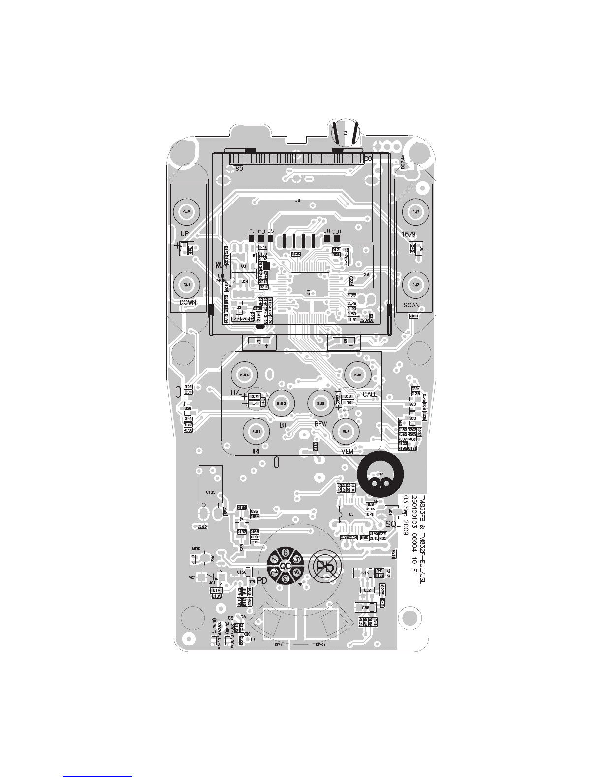
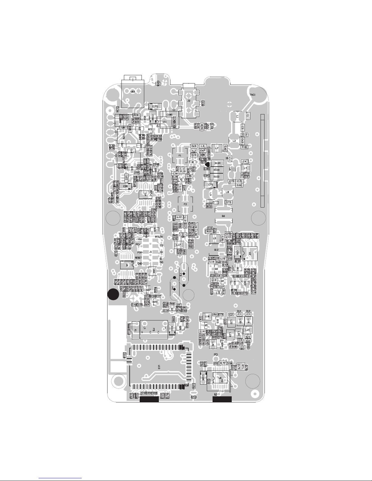
PRINTEDCIRCUITBOARD
MainPCBTopView
VR2
VC1
11
Page 12
PRINTEDCIRCUITBOARD
MainPCBBottomView
L18
L20
12
Page 13
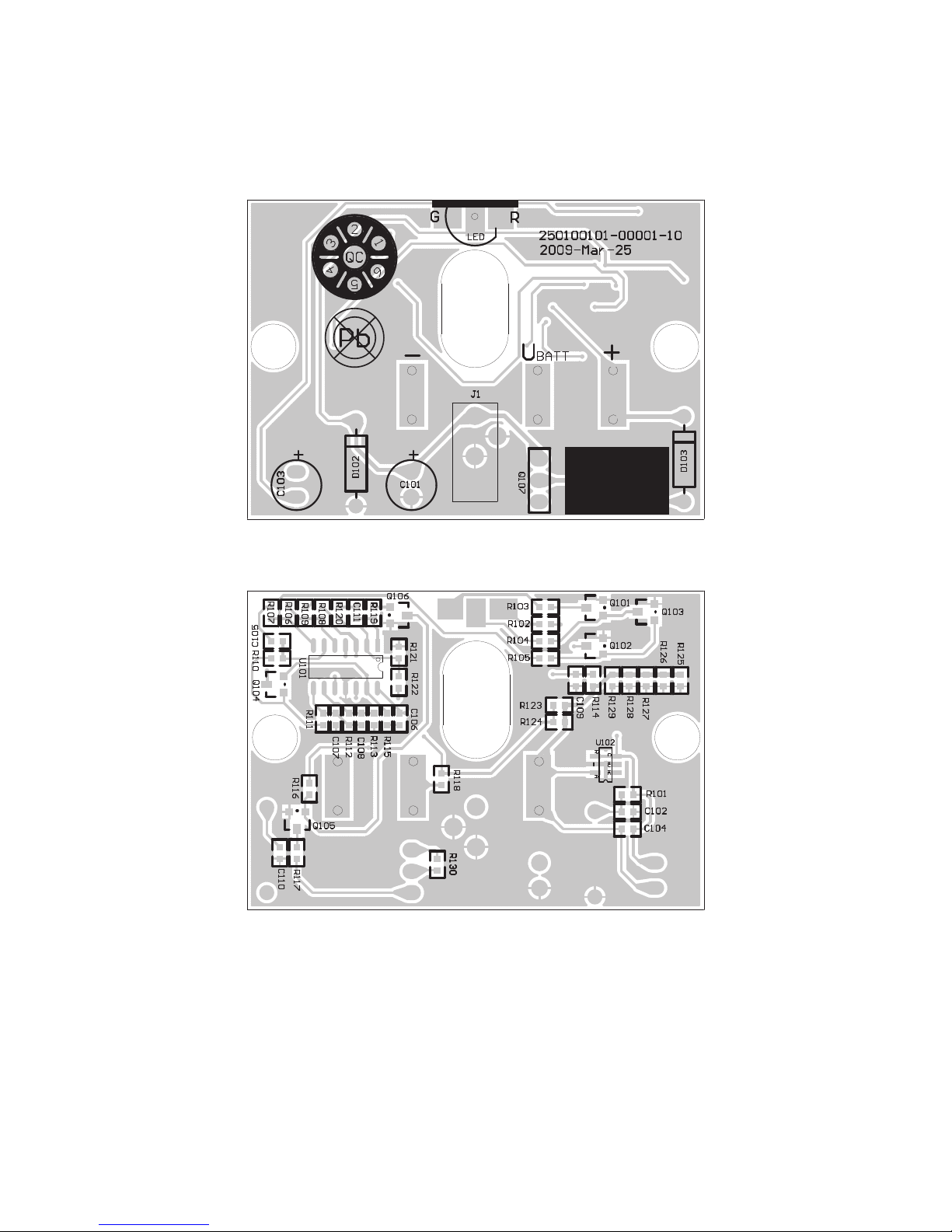
PRINTEDCIRCUITBOARD
CradleChargerPCBView
TopView
BottomView
13
Page 14

TROUBLESHOOTING
Item Symptom Possible Cause
1 Unit does not turn on.
z Defective power switch VR3.
z Check the battery voltage.
z Defective regulator U8.
2
Speaker no sound with
AF signal applied to
volume control
z Defective volume control.
z Defective speaker.
z Defective U11 and/or associated components.
3
Squelch circuit
inoperative
z Check squelch control.
z Defective U1 and/or associated circuitry between pin 9, 10 and
11.
4 No receive (RX)
z Defective regulator U8.
z Check TP1 voltage 0.5 – 4V;
z Check second OSC 20.95MHz, pin9 of U6;
z Defective Q7, Q8, Q2.
z Check U1 audio output voltage at pin 9.
z Defective F1 and F2;
5 Low receiver sensitivity
z Check antenna and connector for possible corrosion or bad
connection.
z Failure of the output from Q7, Q8, Q2, U1
z Check the output level of local OSC.
6 No transmit (TX)
z Defective PTT switch.
z Defective regulator U8.
z Check TP1 voltage 0.5 – 4V;
z Check power transmits circuit Q12, Q6, D1, D2 and Q1;
z Check power control circuit Q17, Q18, Q24;
z Check power control circuit U2;
7 Low RF power output
z Check RF power output from Q6, If it checks good, then check
and antenna switching diode D1, D2.
If not good then check the voltage level outputs of the drive
amplifiers Q3 and Q12 as well as the associated circuitry.
8 Poor or no modulation
z Defective microphone.
z Defective U4 and/or its associated components.
9
Deviation of transmit
frequency
z Check crystal X2and VC1.
14
Page 15
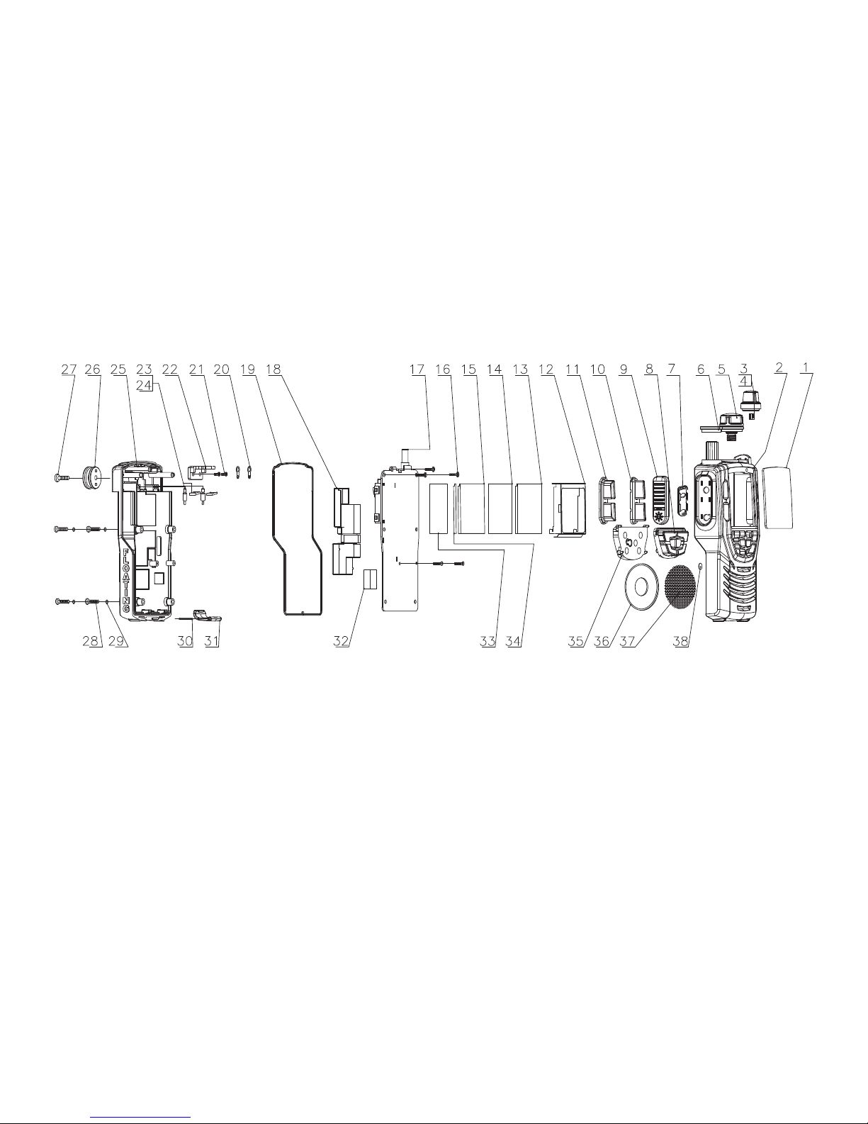
EXPLODEDVIEW(forHH330MainPart)
15
Page 16
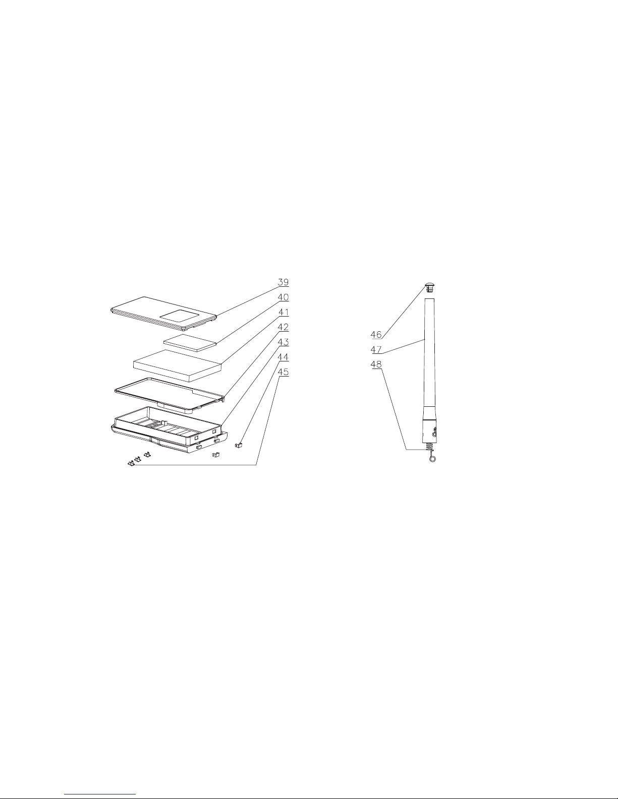
EXPLODEDVIEW(forBatteryand Antenna)
16
Page 17

EXPLODED VIEW LIST
Ref. No. Description Mfr's Part No.
1 D-LENS PMMA MU TM832FUSL 270100034-11002-10
2 P-FCAB MU PC G TM832FUSL DS022 270100030-12002-10
3 P-KEY VOL MU ABS BK TM833FBUSL 3U2X 270100530-11001-10
4 M-SLEE MU SS L5.15 W5 H4.4 SW 260301122-00001-10
5 P-KEY C/F MU ABS BK TM832EUL MIC 3U2X 270101280-12001-10
6 FOAM-HDR RUBB L34.1W26.3T4.7 GREY DS022 320100108-00001-10
7 P-PLATE MU PC BK TM832 PTT MOUNT 3U2X 270102092-12001-10
8 KEY-P MAIN RUB DG 4K TM832FEUL 433U (only for EU) 270200054-11007-10
KEY-P MAIN RUB DG 4K TM832FUSL 433U (only for US) 270200054-11006-10
9 KEY PTT RUB G 1K TM832 270200131-11001-10
10 KEY FUN SR T 2K TM832FEUL RIGHT 433U/201(only for EU) 270200016-11004-10
KEY FUN SR T 2K TM832FUSL RIGHT 433U/201(only for US) 270200016-11003-10
11 KEY FUN SR T 2K TM832FEUL LEFT 433U 270200118-11002-10
12 M-MOUN MU SS L39.3 W37.8 H10.6 LCD 260301094-12001-10
13 LCD TN TSF P 5V 1/4D 1/3B L38.5W37T1.8 - 220100028-00000-10
14 INSU-SHET PVC W L36 W36 D-- ASTIGMATISM 270102604-00001-10
15 D-LENS PMMA MU TM832FEUL Transparent L40 270101425-11002-10
16 SCREW-TS WRH L5 D2 + CZ F RWB (four) 260100191-00000-10
17 TM832FEUL /PCBA MAIN/PCBA /R0 COBRA/EU/G 330202596-00000-10
18 M-COVR MU AL L67 W33.2 H6 260300141-11001-10
19 O-RING MU BK RUB H1.4OD--L118.5W62 3U2X 270200053-12001-10
20 M-WASH MU CU NI L10.55 W1.09 H0.2(two) 260300005-11001-10
21 SCREW-TS RH L8 D2.6 + SUS C (two) 260100022-00000-10
22 M-BRKT MU SS L20 W19 H10 SUS304 260302983-11000-10
23 M-SHAF MU PB GD L10.7 W3.6 H--(two) 260300007-00001-10
24 P-HOLDER MU ABS BK TM833FBUSL CONNECTOR(two) 270100532-11001-10
25 P-RCAB MU PC O TM833FBUSL 021U 270100529-11001-10
26 P-CLIP BU PC BK TM832/TM833 ATTACHMENT 3 270102095-12001-10
27 SCREW-TS RH L10 D3 + BZ SUS F BLACK 260101177-00000-10
28 SCREW-TS PH L12 D-- + BZ SUS F TM832FEUL(four) 260101179-00001-10
29 FOAM-HDR RUBB D1.8T1 NA Black SCREW CAP(five) 320100751-00001-10
30 M-SPPT MU SS L20 W1 H1 LOCK PIN 260301096-00001-10
31 P-COVER MU PC G TM832FEUL GRAY 432U 270100455-12003-10
32 M-SHIE MU TP NI L20.4 W14.1 H8.5 VCO 260301003-00001-10
33 INSU-SHET PVC W L35.4 W33.4 D0.1 TM832FE 270110041-00001-10
34 INSU-SHET PAP S L40 W1.3 D0.1 TM832FEUL (three) 270110039-00001-10
35 P-PLATE MU PMMA BK TM832/TM833 KEYBOARD 270102091-12001-10
36 SPK M 8OHM 1W D40 T5.2 TEK404P-8 OHM1W 290100070-00000-10
37 FOAM-SPK NYL D37.3T-- SS BLACK TM833FBEU 320101847-00001-10
38 INSU-TAPE FILM BK L-- W-- D9.4 WATERPROO 270110368-00000-10
Main Radio Part
17
Page 18

EXPLODED VIEW LIST - CONTINUED
Battery Part
Ref. No. Description Mfr's Part No.
39 P-BATT-DR BU ABS G TM832FEUL GRAY 432U 270101071-12002-10
40 FOAM-HDR SPNG L40W8T1 Black (two) 320100666-00001-10
41 BAT-R PRISM LI 7.4V 1000MAH TP603450 TEC 230400180-00000-10
42 O-RING BD BK RUB H5.4OD--L94.05W59 270200380-13001-10
43 P-RCAB BT ABS G TM832FEUL GRAY 432U 270100953-11002-10
44 CON-COMM PB T0.2H5WD-- GD C(two) 260300377-11001-10
45 CON-CHAR PB T0.2H3.5WD-- GD UNIT(three) 260300380-11001-10
Antenna Par
t
Location Codes Description Mfr's Part No.
46 P-CAP BU ABS BK TM833/832 ANT 3U2X 270102110-11001-10
47 P-SLV-ANT BU PU BK TM832EUL ANT 3U2X 270102093-12001-10
48 SPRING COS ANT SW CU WD1 L158.5 OD:6.8MM 260200009-00000-10
18
Page 19

Location Codes
Description
Mfr's Part No.
TM832FEUL /U- U-M /R0 COBRA/EU
330100055-00000-10
TM832FEUL /U- MAIN/UNIT /R0 COBRA/EU
330100060-00000-10
17
TM832FEUL /PCBA MAIN/PCBA /R0 COBRA/EU/G
330202596-00000-10
13
LCD TN TSF P 5V 1/4D 1/3B L38.5W37T1.8 -
220100028-00000-10
RUBCON SRI PIT0.10 L30.1 W2.0 H5.2
240300313-00000-10
18
M-COVR MU AL L67 W33.2 H6
260300141-11001-10
32
M-SHIE MU TP NI L20.4 W14.1 H8.5 VCO
260301003-00001-10
12
M-MOUN MU SS L39.3 W37.8 H10.6 LCD
260301094-12001-10
15
D-LENS PMMA MU TM832FEUL Transparent L40
270101425-11002-10
14
INSU-SHET PVC W L36 W36 D-- ASTIGMATISM
270102604-00001-10
INLAY MKEY PVC L34 W22 TM832/TM833 UNIT
270102692-11001-10
INLAY MKEY PET L25.4 W7.6 TM832/833 (two)
270102693-11001-10
34
INSU-SHET PAP S L40 W1.3 D0.1 TM832FEUL (three)
270110039-00001-10
33
INSU-SHET PVC W L35.4 W33.4 D0.1 TM832FE
270110041-00001-10
FOAM-CUH SILI L12W6.5T3 GREY
320100009-00001-10
FOAM-HDR SPNG L40W4T3 Grey (four)
320100664-00001-10
FOAM-CUH SPNG L9W7T1 White
320100696-00000-10
TM832FEUL /PCBA MAIN/SOLDERING/PCBA /R0
330201924-00000-10
MIC CDR -O -52dB 3V D9.7 T4.5 LYS-M9745-
290100001-00000-10
C109
CAP-RELE 100 uF M 10V D5 H8
280201079-00000-10
C178
CAP-RELE 100 uF M 10V D5 H8
280201079-00000-10
C179
CAP-RELE 100 uF M 10V D5 H8
280201079-00000-10
C180
CAP-RELE 100 uF M 16V D6 H5
280201082-00000-10
C185
CAP-RELE 10 uF M 25V D4 H5
280201073-00000-10
F3
XTL 21.4M 2.5 2pF L3.2 W8 H6 -20C ~ 70C
280700099-00000-10
F4
XTL 21.4M 2.5 2pF L3.2 W8 H6 -20C ~ 70C
280700099-00000-10
F5
FLTR-REC LEAD 450 K +/-7.5 KHz@ 6dB LTM4
280700243-00000-10
VR3
VR-ST LOG 10 Kohm P DIP H R A;JIS;W/S
280101743-00000-10
X1
FLTR-REC LEAD 450 K +/-4 KHz@ 3dB CDB450
280700253-00000-10
X2
XTL 20.95M 2.5 15pF L8 W7.8 H3 -30C ~ 50
280700161-00000-10
X3
XTL 7.3728 M 30 12.5pF D3.0 H8.0 -10+60
280700031-00000-10
TM832EUL /COBA LCD BONDING PCBA /R0 COBR
330301732-00000-10
U401
A-IC ANA HT1621(DICE-SD1706) CHIP 48 BON
210100060-00000-10
TM832EUL /SMTA LCD PCBA /R0 COBRA-EUR
330401965-00000-10
PCB DS FR4 GP LCD3 L32W20T1
250100356-00003-10
C401
CAP-CCER 100 nF K 16 VDC 0402 X7R
280200343-00000-10
C407
CAP-CCER 100 nF K 16 VDC 0402 X7R
280200343-00000-10
C409
CAP-CCER 1000 pF K 50 VDC 0402 X7R 1570-
280200327-00000-10
R401
RES TFC 4.7 Kohm 0402 J 1/16W
280101287-00000-10
R402
RES TFC 100 ohm 0402 J 1/16W
280100919-00000-10
TM832EUL /SMTA PTT PCBA /R0 COBRA-EUR
330401964-00000-10
SW-TACT SMD V 12V 5mA TSUY-2SL 1P2T HUA (two)
240400313-00000-10
PCB DS FR4 GP PTT2 L33W8T1
250100355-00002-10
TM832FEUL /SMTA MAIN/TOP/SMD/PCBA /R0 CO
330401412-00000-10
C14
CAP-CCER 27 pF J 50 VDC 0603 COG
280200800-00000-10
C31
CAP-CCER 1000 pF K 50 VDC 0402 X7R 1570-
280200327-00000-10
C33
CAP-CCER 1000 pF K 50 VDC 0402 X7R 1570-
280200327-00000-10
C35
CAP-CCER 1000 pF K 50 VDC 0402 X7R 1570-
280200327-00000-10
C37
CAP-CCER 1000 pF K 50 VDC 0402 X7R 1570-
280200327-00000-10
C40
CAP-CCER 1000 pF K 50 VDC 0402 X7R 1570-
280200327-00000-10
C41
CAP-CCER 1000 pF K 50 VDC 0402 X7R 1570-
280200327-00000-10
C54
CAP-CCER 1000 pF K 50 VDC 0402 X7R 1570-
280200327-00000-10
C61
CAP-CCER 100 nF K 16 VDC 0402 X7R
280200343-00000-10
PARTS LIST (HH330 EU)
Main PCB Assembly
19
Page 20

Location Codes
Description
Mfr's Part No.
C71
CAP-CCER 56 pF J 50 VDC 0402 COG
280200859-00000-10
C100
CAP-CCER 470 pF J 50 VDC 0402 COG
280200840-00000-10
C101
CAP-CCER 470 pF J 50 VDC 0402 COG
280200840-00000-10
C102
CAP-CCER 470 pF J 50 VDC 0402 COG
280200840-00000-10
C110
CAP-CCER 2 pF C 50 VDC 0402 COG
280200779-00000-10
C113
CAP-CCER 100 nF K 16 VDC 0402 X7R
280200343-00000-10
C114
CAP-CCER 100 nF K 16 VDC 0402 X7R
280200343-00000-10
C117
CAP-CCER 100 nF K 16 VDC 0402 X7R
280200343-00000-10
C118
CAP-CCER 100 nF K 16 VDC 0402 X7R
280200343-00000-10
C119
CAP-CCER 100 nF K 16 VDC 0402 X7R
280200343-00000-10
C120
CAP-CCER 100 nF K 16 VDC 0402 X7R
280200343-00000-10
C126
CAP-CCER 100 nF K 16 VDC 0402 X7R
280200343-00000-10
C129
CAP-CCER 100 nF K 16 VDC 0402 X7R
280200343-00000-10
C136
CAP-CCER 220 nF Z 16 VDC 0402 Y5V
280200303-00000-10
C137
CAP-CCER 33 nF K 16 VDC 0402 X7R
280200428-00000-10
C138
CAP-CCER 33 nF K 16 VDC 0402 X7R
280200428-00000-10
C139
CAP-CCER 33 nF K 16 VDC 0402 X7R
280200428-00000-10
C141
CAP-CCER 220 pF J 50 VDC 0402 COG
280200786-00000-10
C142
CAP-CCER 220 pF J 50 VDC 0402 COG
280200786-00000-10
C146
CAP-CCER 820 pF J 50 VDC 0402 COG
280200888-00000-10
C153
CAP-CCER 1000 pF K 50 VDC 0402 X7R 1570-
280200327-00000-10
C166 CAP-CCER 47 nF K 25 VDC 0402 X7R 280200453-00000-10
C168
CAP-CTAN 2.2 uF M 16 VDC CASEA
280201248-00000-10
C176
CAP-CCER 10 pF J 50 VDC 0402 NPO 1570-03
280200583-00000-10
C177
CAP-CCER 10 pF J 50 VDC 0402 NPO 1570-03
280200583-00000-10
C181
CAP-CCER 100 nF K 16 VDC 0402 X7R
280200343-00000-10
C199
CAP-CCER 3 pF C 50 VDC 0402 COG
280200811-00000-10
C203
CAP-CCER 1000 pF K 50 VDC 0402 X7R 1570-
280200327-00000-10
C208
CAP-CCER 100 nF K 16 VDC 0402 X7R
280200343-00000-10
C209
CAP-CCER 100 nF K 16 VDC 0402 X7R
280200343-00000-10
C217
CAP-CCER 100 nF K 16 VDC 0402 X7R
280200343-00000-10
C225
CAP-CCER 1 uF Z 10 VDC 0603 Y5V
280200293-00000-10
C227
CAP-CCER 1000 pF K 50 VDC 0402 X7R 1570-
280200327-00000-10
C233
CAP-CCER 1000 pF K 50 VDC 0402 X7R 1570-
280200327-00000-10
C234
CAP-CCER 1000 pF K 50 VDC 0402 X7R 1570-
280200327-00000-10
C236
CAP-CCER 1000 pF K 50 VDC 0402 X7R 1570-
280200327-00000-10
C237
CAP-CCER 100 nF K 16 VDC 0402 X7R
280200343-00000-10
C242
CAP-CCER 1000 pF K 50 VDC 0402 X7R 1570-
280200327-00000-10
C243
CAP-CCER 100 nF K 16 VDC 0402 X7R
280200343-00000-10
C244
CAP-CCER 100 pF J 50 VDC 0402 COG 1553-0
280200729-00000-10
C245
CAP-CCER 100 pF J 50 VDC 0402 COG 1553-0
280200729-00000-10
C246
CAP-CCER 100 nF K 16 VDC 0402 X7R
280200343-00000-10
C247
CAP-CCER 100 nF K 16 VDC 0402 X7R
280200343-00000-10
D3
LED- SMD- 0805 OR 2.1V 200mcd KPA-3010SE
280500100-00000-10
D4
LED- SMD- 0805 OR 2.1V 200mcd KPA-3010SE
280500100-00000-10
D5
LED- SMD- 0603 OR 2.1V 20mcd
280500008-00000-10
D6
LED- SMD- 0603 OR 2.1V 20mcd
280500008-00000-10
D7
LED- SMD- 0603 OR 2.1V 20mcd
280500008-00000-10
D8
LED- SMD- 0603 OR 2.1V 20mcd
280500008-00000-10
L31
IND-SMD 2.2 uH +-10% Q35 0603 SDFL1608Q2
280300666-00000-10
Q9
TRS-BP PNP SOT23 MMBT3906LT1 4823-30669-
280400122-00000-10
Q26
TRS-BP PNP SOT23 MMBT3906LT1 4823-30669-
280400122-00000-10
PARTS LIST (HH330 EU)- CONTINUED
Main PCB Assembly
20
Page 21

Location Codes
Description
Mfr's Part No.
Q28
TRS-BP NPN SOT23 MMBT3904LT1
280400121-00000-10
Q30
TRS-BP NPN SOT23 MMBT3904LT1
280400121-00000-10
R9
RES TFC 4.7 Kohm 0402 J 1/16W
280101287-00000-10
R23
RES TFC 68 ohm 0402 J 1/16W
280101403-00000-10
R26
RES TFC 4.7 Kohm 0402 J 1/16W
280101287-00000-10
R40
RES TFC 10 Kohm 0402 J 1/16W
280100937-00000-10
R41
RES TFC 47 ohm 0402 J 1/16W
280101305-00000-10
R42
RES TFC 10 Kohm 0402 J 1/16W
280100937-00000-10
R53
RES TFC 1 Kohm 0402 J 1/16W
280100929-00000-10
R58 RES TFC 100 ohm 0402 J 1/16W 280100919-00000-10
R59 RES TFC 100 ohm 0402 J 1/16W 280100919-00000-10
R61 RES TFC 100 ohm 0402 J 1/16W 280100919-00000-10
R62
RES TFC 1 Kohm 0402 J 1/16W
280100929-00000-10
R63
RES TFC 1 Kohm 0402 J 1/16W
280100929-00000-10
R77
RES TFC 3.3 Kohm 0402 J 1/16W
280101201-00000-10
R79
RES TFC 2.2 Kohm 0402 J 1/16W
280101100-00000-10
R86
RES TFC 2.2 Kohm 0402 J 1/16W
280101100-00000-10
R87
RES TFC 2.2 Kohm 0402 J 1/16W
280101100-00000-10
R89
RES TFC 3.3 Kohm 0402 J 1/16W
280101201-00000-10
R90
RES TFC 300 Kohm 0402 J 1/16W
280101186-00000-10
R91
RES TFC 200 Kohm 0402 F 1/16W
280101079-00000-10
R121
RES TFC 3.3 Kohm 0402 J 1/16W
280101201-00000-10
R122
RES TFC 10 Kohm 0402 J 1/16W
280100937-00000-10
R123
RES TFC 10 Kohm 0402 J 1/16W
280100937-00000-10
R127
RES TFC 10 Kohm 0402 J 1/16W
280100937-00000-10
R132
RES TFC 47 Kohm 0402 J 1/16W
280101294-00000-10
R134
RES TFC 10 Kohm 0402 J 1/16W
280100937-00000-10
R138
RES TFC 47 ohm 0402 J 1/16W
280101305-00000-10
R148
RES TFC 200 Kohm 0402 F 1/16W
280101079-00000-10
R149
RES TFC 100 Kohm 0402 F 1/16W
280100939-00000-10
R153
RES TFC 1 Kohm 0402 J 1/16W
280100929-00000-10
R154
RES TFC 2.2 Kohm 0402 J 1/16W
280101100-00000-10
R156
RES TFC 1 Kohm 0402 J 1/16W
280100929-00000-10
R162
RES TFC 22 Kohm 0402 J 1/16W
280101107-00000-10
R163
RES TFC 22 Kohm 0402 J 1/16W
280101107-00000-10
R171
RES TFC 47 Kohm 0402 J 1/16W
280101294-00000-10
R174
RES TFC 1 Kohm 0402 J 1/16W
280100929-00000-10
R175
RES TFC 10 Kohm 0402 J 1/16W
280100937-00000-10
R179
RES TFC 150 ohm 0402 J 1/16W
280101007-00000-10
R182
RES TFC 10 Kohm 0402 J 1/16W
280100937-00000-10
R183 RES TFC 220 ohm 0402 J 1/16W 280101096-00000-10
R184
RES TFC 5.6 Kohm 0402 J 1/16W
280101346-00000-10
R185
RES TFC 5.6 Kohm 0402 J 1/16W
280101346-00000-10
R187
RES TFC 12 Kohm 0402 J 1/6W
280100981-00000-10
R188
RES TFC 12 Kohm 0402 J 1/6W
280100981-00000-10
R189
RES TFC 68 Kohm 0402 J 1/16W
280101395-00000-10
R190
RES TFC 68 Kohm 0402 J 1/16W
280101395-00000-10
R194
RES TFC 4.7 Kohm 0402 J 1/16W
280101287-00000-10
R195
RES TFC 4.7 Kohm 0402 J 1/16W
280101287-00000-10
R196
RES TFC 2.2 Kohm 0402 J 1/16W
280101100-00000-10
R197
RES TFC 2.2 Kohm 0402 J 1/16W
280101100-00000-10
PARTS LIST (HH330 EU)- CONTINUED
Main PCB Assembly
21
Page 22

Location Codes
Description
Mfr's Part No.
R202
RES TFC 47 Kohm 0402 J 1/16W
280101294-00000-10
R203
RES TFC 10 Kohm 0402 J 1/16W
280100937-00000-10
R207
RES TFC 10 Kohm 0402 J 1/16W
280100937-00000-10
R208
RES TFC 150 ohm 0402 J 1/16W
280101007-00000-10
R209
RES TFC 4.7 Kohm 0402 J 1/16W
280101287-00000-10
R211
RES TFC 0 ohm 0402 J 1/16W
280100909-00000-10
R217
RES TFC 330 ohm 0402 J 1/16W
280101196-00000-10
R219
RES TFC 330 ohm 0402 J 1/16W
280101196-00000-10
R220
RES TFC 330 ohm 0402 J 1/16W
280101196-00000-10
R304
RES TFC 0 ohm 0402 J 1/16W
280100909-00000-10
RT2
THERM- NTC 10 Kohm +/-1% SMD 125TO -40C
280800011-00000-10
U1
O-IC RF BA4116FV SOT23 16
210100475-00000-10
U3
O-IC PWR XC61CN2702MR SOT23 3 TOREX
210100586-00000-10
U7
C-IC MMCU TQFP 64 PIC24FJ64GA006-I/PT MI
210201346-00000-10
U14
M-IC MEM AT24C16BN-SH-T SOIC 8
210100399-00000-10
VC1
CAP-TRM 3 pF- 10 pF 100V SMD N750 TZC3R1
280202416-00000-10
VR1
VR-ST LIN 10 Kohm P 0.15W SMD H R EVM3YS
280101763-00000-10
VR2
VR-ST LIN 50 Kohm P 0.15W SMD V R EVM3YS
280101767-00000-10
TM833FBEUL /SMTA MAIN/BTM/SMD/PCBA /R0 C
330400028-00000-10
PCB 4L FR4 GP MAIN 1-4 L112.5W57T1.0 L2-
250100103-00004-10
C1
CAP-CCER 18 pF J 50 VDC 0603 COG
280200768-00000-10
C2
CAP-CCER 30 pF J 50 VDC 0402 COG
280200807-00000-10
C3
CAP-CCER 30 pF J 50 VDC 0402 COG
280200807-00000-10
C4
CAP-CCER 10 pF J 50 VDC 0603 COG
280200728-00000-10
C5
CAP-CCER 10 pF J 50 VDC 0603 COG
280200728-00000-10
C6
CAP-CCER 10 pF J 50 VDC 0402 NPO 1570-03
280200583-00000-10
C7
CAP-CCER 10 pF J 50 VDC 0402 NPO 1570-03
280200583-00000-10
C8
CAP-CCER 10 pF J 50 VDC 0402 NPO 1570-03
280200583-00000-10
C9
CAP-CCER 3 pF C 50 VDC 0402 COG
280200811-00000-10
C10
CAP-CCER 10 pF J 50 VDC 0402 NPO 1570-03
280200583-00000-10
C11
CAP-CCER 10 pF J 50 VDC 0402 NPO 1570-03
280200583-00000-10
C12
CAP-CCER 33 pF J 50 VDC 0603 NPO
280200236-00000-10
C13
CAP-CCER 100 pF J 50 VDC 0402 COG 1553-0
280200729-00000-10
C15
CAP-CCER 47 pF J 50 VDC 0603 COG
280200839-00000-10
C16
CAP-CCER 47 pF J 50 VDC 0603 COG
280200839-00000-10
C17
CAP-CCER 47 pF J 50 VDC 0402 COG
280200838-00000-10
C18
CAP-CCER 1000 pF K 50 VDC 0402 X7R 1570-
280200327-00000-10
C19
CAP-CCER 1000 pF K 50 VDC 0402 X7R 1570-
280200327-00000-10
C20
CAP-CCER 1000 pF K 50 VDC 0603 X7R
280200328-00000-10
C21
CAP-CCER 1000 pF K 50 VDC 0402 X7R 1570-
280200327-00000-10
C22
CAP-CCER 1000 pF K 50 VDC 0603 X7R
280200328-00000-10
C23
CAP-CCER 1000 pF K 50 VDC 0402 X7R 1570-
280200327-00000-10
C24
CAP-CCER 1000 pF K 50 VDC 0402 X7R 1570-
280200327-00000-10
C25
CAP-CCER 1000 pF K 50 VDC 0402 X7R 1570-
280200327-00000-10
C26
CAP-CCER 1000 pF K 50 VDC 0402 X7R 1570-
280200327-00000-10
C27
CAP-CCER 1000 pF K 50 VDC 0402 X7R 1570-
280200327-00000-10
C28
CAP-CCER 1000 pF K 50 VDC 0402 X7R 1570-
280200327-00000-10
C29
CAP-CCER 1000 pF K 50 VDC 0402 X7R 1570-
280200327-00000-10
C30
CAP-CCER 1000 pF K 50 VDC 0402 X7R 1570-
280200327-00000-10
C32
CAP-CCER 10 nF K 25 VDC 0402 X7R
280200336-00000-10
C34
CAP-CCER 1000 pF K 50 VDC 0402 X7R 1570-
280200327-00000-10
C36
CAP-CCER 1000 pF K 50 VDC 0402 X7R 1570-
280200327-00000-10
C38
CAP-CCER 1000 pF K 50 VDC 0402 X7R 1570-
280200327-00000-10
PARTS LIST (HH330 EU)- CONTINUED
Main PCB Assembly
22
Page 23

Location Codes
Description
Mfr's Part No.
C39
CAP-CCER 1000 pF K 50 VDC 0402 X7R 1570-
280200327-00000-10
C42
CAP-CCER 100 nF K 16 VDC 0402 X7R
280200343-00000-10
C43
CAP-CCER 1000 pF K 50 VDC 0402 X7R 1570-
280200327-00000-10
C44
CAP-CCER 100 nF K 16 VDC 0402 X7R
280200343-00000-10
C45
CAP-CCER 1000 pF K 50 VDC 0402 X7R 1570-
280200327-00000-10
C46
CAP-CCER 1000 pF K 50 VDC 0402 X7R 1570-
280200327-00000-10
C47
CAP-CCER 1000 pF K 50 VDC 0402 X7R 1570-
280200327-00000-10
C48
CAP-CCER 1000 pF K 50 VDC 0402 X7R 1570-
280200327-00000-10
C49
CAP-CCER 1000 pF K 50 VDC 0402 X7R 1570-
280200327-00000-10
C50
CAP-CCER 1000 pF K 50 VDC 0402 X7R 1570-
280200327-00000-10
C51
CAP-CCER 1000 pF K 50 VDC 0402 X7R 1570-
280200327-00000-10
C52
CAP-CCER 1000 pF K 50 VDC 0402 X7R 1570-
280200327-00000-10
C53
CAP-CCER 10 nF K 25 VDC 0402 X7R
280200336-00000-10
C55
CAP-CCER 1000 pF K 50 VDC 0402 X7R 1570-
280200327-00000-10
C56
CAP-CCER 1 uF Z 6.3 VDC 0402 Y5V
280200290-00000-10
C57
CAP-CCER 1000 pF K 50 VDC 0402 X7R 1570-
280200327-00000-10
C58
CAP-CCER 1000 pF K 50 VDC 0402 X7R 1570-
280200327-00000-10
C59
CAP-CCER 1000 pF K 50 VDC 0402 X7R 1570-
280200327-00000-10
C60
CAP-CCER 1000 pF K 50 VDC 0402 X7R 1570-
280200327-00000-10
C62
CAP-CCER 12 pF J 50 VDC 0603 COG
280200742-00000-10
C63
CAP-CCER 12 pF J 50 VDC 0603 COG
280200742-00000-10
C64
CAP-CCER 47 pF J 50 VDC 0402 COG
280200838-00000-10
C65
CAP-CCER 560 pF J 50 VDC 0402 COG
280200861-00000-10
C66
CAP-CCER 27 pF J 50 VDC 0603 COG
280200800-00000-10
C67
CAP-CCER 18 pF J 50 VDC 0603 COG
280200768-00000-10
C68
CAP-CCER 22 pF J 50 VDC 0402 COG
280200783-00000-10
C69
CAP-CCER 22 pF J 50 VDC 0402 COG
280200783-00000-10
C70
CAP-CCER 68 pF J 50 VDC 0603 NPO
280200268-00000-10
C72
CAP-CCER 22 pF J 50 VDC 0603 NPO
280200214-00000-10
C73
CAP-CCER 8 pF D 50 VDC 0402 COG
280200883-00000-10
C74
CAP-CCER 8 pF D 50 VDC 0402 COG
280200883-00000-10
C75
CAP-CTAN 2.2 uF M 16 VDC CASEA
280201248-00000-10
C76
CAP-CTAN 2.2 uF M 16 VDC CASEA
280201248-00000-10
C77
CAP-CCER 33 pF J 50 VDC 0603 NPO
280200236-00000-10
C79
CAP-CCER 10 nF K 25 VDC 0402 X7R
280200336-00000-10
C80
CAP-CCER 10 nF K 25 VDC 0402 X7R
280200336-00000-10
C81
CAP-CCER 10 nF K 25 VDC 0402 X7R
280200336-00000-10
C82
CAP-CCER 10 nF K 25 VDC 0402 X7R
280200336-00000-10
C83
CAP-CCER 10 nF K 25 VDC 0402 X7R
280200336-00000-10
C84
CAP-CCER 10 nF K 25 VDC 0402 X7R
280200336-00000-10
C85
CAP-CCER 10 nF K 25 VDC 0402 X7R
280200336-00000-10
C86
CAP-CCER 10 nF K 25 VDC 0402 X7R
280200336-00000-10
C87
CAP-CCER 10 nF K 25 VDC 0402 X7R
280200336-00000-10
C89
CAP-CCER 1800 pF K 50 VDC 0402 X7R
280200379-00000-10
C90
CAP-CCER 2200 pF K 50 VDC 0402 X7R 1570-
280200169-00000-10
C91
CAP-CCER 10 nF K 25 VDC 0402 X7R
280200336-00000-10
C92
CAP-CCER 1 uF Z 6.3 VDC 0402 Y5V
280200290-00000-10
C93
CAP-CCER 470 pF J 50 VDC 0402 COG
280200840-00000-10
C94
CAP-CCER 100 nF K 16 VDC 0402 X7R
280200343-00000-10
C95
CAP-CTAN 10 uF K 6.3 VDC CASEA
280201318-00000-10
C96
CAP-CCER 10 nF K 25 VDC 0402 X7R
280200336-00000-10
C97
CAP-CCER 470 pF J 50 VDC 0402 COG
280200840-00000-10
C98
CAP-CCER 10 nF K 25 VDC 0402 X7R
280200336-00000-10
PARTS LIST (HH330 EU)- CONTINUED
Main PCB Assembly
23
Page 24

Location Codes
Description
Mfr's Part No.
C99
CAP-CCER 470 pF J 50 VDC 0402 COG
280200840-00000-10
C103
CAP-CCER 470 pF J 50 VDC 0402 COG
280200840-00000-10
C104
CAP-CCER 1.5 pF C 50 VDC 0402 COG
280200760-00000-10
C105
CAP-CCER 100 pF J 50 VDC 0402 COG 1553-0
280200729-00000-10
C106
CAP-CCER 100 pF J 50 VDC 0402 COG 1553-0
280200729-00000-10
C107
CAP-CCER 100 pF J 50 VDC 0402 COG 1553-0
280200729-00000-10
C108
CAP-CCER 10 nF K 25 VDC 0402 X7R
280200336-00000-10
C111
CAP-CTAN 22 uF M 10 VDC CASEA
280201245-00000-10
C112
CAP-CCER 100 nF K 16 VDC 0402 X7R
280200343-00000-10
C115
CAP-CCER 1000 pF K 50 VDC 0402 X7R 1570-
280200327-00000-10
C116
CAP-CCER 220 nF Z 16 VDC 0402 Y5V
280200303-00000-10
C121
CAP-CCER 100 nF K 16 VDC 0402 X7R
280200343-00000-10
C122
CAP-CCER 1 uF Z 6.3 VDC 0402 Y5V
280200290-00000-10
C123
CAP-CCER 100 nF K 16 VDC 0402 X7R
280200343-00000-10
C124
CAP-CCER 1 uF Z 6.3 VDC 0402 Y5V
280200290-00000-10
C125
CAP-CCER 100 nF K 16 VDC 0402 X7R
280200343-00000-10
C127
CAP-CCER 100 nF K 16 VDC 0402 X7R
280200343-00000-10
C128
CAP-CCER 100 nF K 16 VDC 0402 X7R
280200343-00000-10
C130
CAP-CCER 100 nF K 16 VDC 0402 X7R
280200343-00000-10
C131
CAP-CCER 100 nF K 16 VDC 0402 X7R
280200343-00000-10
C132
CAP-CCER 100 nF K 16 VDC 0402 X7R
280200343-00000-10
C133
CAP-CCER 100 nF K 16 VDC 0402 X7R
280200343-00000-10
C134
CAP-CCER 100 nF K 16 VDC 0402 X7R
280200343-00000-10
C135
CAP-CCER 100 nF K 16 VDC 0402 X7R
280200343-00000-10
C140
CAP-CCER 100 nF K 16 VDC 0402 X7R
280200343-00000-10
C143
CAP-CCER 220 pF J 50 VDC 0402 COG
280200786-00000-10
C144
CAP-CCER 100 nF K 16 VDC 0402 X7R
280200343-00000-10
C145
CAP-CCER 220 pF J 50 VDC 0402 COG
280200786-00000-10
C147
CAP-CCER 56 pF J 50 VDC 0603 UJ
280200901-00000-10
C148
CAP-CCER 4700 pF K 50 VDC 0402 X7R
280200447-00000-10
C149
CAP-CCER 10 nF K 25 VDC 0402 X7R
280200336-00000-10
C150
CAP-CCER 1000 pF K 50 VDC 0402 X7R 1570-
280200327-00000-10
C151
CAP-CCER 470 pF J 50 VDC 0402 COG
280200840-00000-10
C152
CAP-CCER 15 pF J 50 VDC 0402 COG
280200756-00000-10
C154
CAP-CCER 10 nF K 25 VDC 0402 X7R
280200336-00000-10
C155
CAP-CCER 10 nF K 25 VDC 0402 X7R
280200336-00000-10
C156
CAP-CCER 180 pF J 50 VDC 0402 COG
280200770-00000-10
C157
CAP-CCER 3 pF C 50 VDC 0402 COG
280200811-00000-10
C158
CAP-CCER 5 pF C 50 VDC 0402 COG
280200852-00000-10
C159
CAP-CCER 5 pF C 50 VDC 0402 COG
280200852-00000-10
C160
CAP-CCER 1 pF C 50 VDC 0402 COG
280200734-00000-10
C161
CAP-CCER 1.2 pF C 50 VDC 0402 COG
280200750-00000-10
C162
CAP-CCER 3300 pF K 50 VDC 0402 X7R 1570-
280200423-00000-10
C163
CAP-CCER 10 nF K 25 VDC 0402 X7R
280200336-00000-10
C164
CAP-CCER 100 nF K 16 VDC 0402 X7R
280200343-00000-10
C165
CAP-CCER 47 nF K 25 VDC 0402 X7R
280200453-00000-10
C167
CAP-CCER 47 nF K 25 VDC 0402 X7R
280200453-00000-10
C169
CAP-CTAN 22 uF M 10 VDC CASEA
280201245-00000-10
C170
CAP-CTAN 22 uF M 10 VDC CASEA
280201245-00000-10
C171
CAP-CCER 1 uF Z 6.3 VDC 0402 Y5V
280200290-00000-10
C172
CAP-CCER 1 uF Z 6.3 VDC 0402 Y5V
280200290-00000-10
C173
CAP-CCER 220 pF J 50 VDC 0402 COG
280200786-00000-10
C174
CAP-CCER 22 pF G 50 VDC 0603 NPO
280200638-00000-10
PARTS LIST (HH330 EU)- CONTINUED
Main PCB Assembly
24
Page 25

Location Codes
Description
Mfr's Part No.
C175
CAP-CCER 8 pF D 50 VDC 0402 COG
280200883-00000-10
C182
CAP-CCER 3300 pF K 50 VDC 0402 X7R 1570-
280200423-00000-10
C183
CAP-CCER 1000 pF K 50 VDC 0402 X7R 1570-
280200327-00000-10
C184
CAP-CCER 1000 pF K 50 VDC 0402 X7R 1570-
280200327-00000-10
C186
CAP-CTAN 10 uF K 6.3 VDC CASEA
280201318-00000-10
C187
CAP-CCER 4700 pF K 50 VDC 0402 X7R
280200447-00000-10
C188
CAP-CCER 100 nF K 16 VDC 0402 X7R
280200343-00000-10
C189
CAP-CCER 470 nF Z 10 VDC 0402 Y5V
280200317-00000-10
C190
CAP-CCER 2200 pF K 50 VDC 0402 X7R 1570-
280200169-00000-10
C191
CAP-CCER 1 uF Z 6.3 VDC 0402 Y5V
280200290-00000-10
C192
CAP-CCER 100 nF K 16 VDC 0402 X7R
280200343-00000-10
C193
CAP-CCER 470 pF J 50 VDC 0402 COG
280200840-00000-10
C194
CAP-CCER 1000 pF K 50 VDC 0402 X7R 1570-
280200327-00000-10
C195
CAP-CCER 1 uF Z 6.3 VDC 0402 Y5V
280200290-00000-10
C196
CAP-CCER 1 uF Z 6.3 VDC 0402 Y5V
280200290-00000-10
C197
CAP-CCER 1000 pF K 50 VDC 0402 X7R 1570-
280200327-00000-10
C198
CAP-CCER 2 pF C 50 VDC 0402 COG
280200779-00000-10
C200
CAP-CCER 10 pF J 50 VDC 0603 COG
280200728-00000-10
C201
CAP-CCER 1000 pF K 50 VDC 0402 X7R 1570-
280200327-00000-10
C202
CAP-CCER 1000 pF K 50 VDC 0402 X7R 1570-
280200327-00000-10
C204
CAP-CCER 47 nF K 25 VDC 0402 X7R
280200453-00000-10
C205
CAP-CCER 47 nF K 25 VDC 0402 X7R
280200453-00000-10
C206
CAP-CCER 470 pF J 50 VDC 0402 COG
280200840-00000-10
C207
CAP-CCER 100 nF K 16 VDC 0402 X7R
280200343-00000-10
C210
CAP-CCER 100 nF K 16 VDC 0402 X7R
280200343-00000-10
C211
CAP-CCER 2 pF C 50 VDC 0402 COG
280200779-00000-10
C212
CAP-CCER 100 nF K 16 VDC 0402 X7R
280200343-00000-10
C214
CAP-CCER 18 pF J 50 VDC 0402 COG
280200767-00000-10
C215
CAP-CCER 1000 pF K 50 VDC 0402 X7R 1570-
280200327-00000-10
C218
CAP-CCER 10 nF K 25 VDC 0402 X7R
280200336-00000-10
C219
CAP-CCER 100 nF K 16 VDC 0402 X7R
280200343-00000-10
C220
CAP-CCER 470 nF Z 10 VDC 0402 Y5V
280200317-00000-10
C221
CAP-CCER 100 nF K 16 VDC 0402 X7R
280200343-00000-10
C222
CAP-CCER 5 pF C 50 VDC 0402 COG
280200852-00000-10
C223
CAP-CCER 4.7 pF B 50 VDC 0402 COG
280200848-00000-10
C224
CAP-CCER 47 pF J 50 VDC 0402 COG
280200838-00000-10
C226
CAP-CCER 4700 pF K 50 VDC 0402 X7R
280200447-00000-10
C228
CAP-CCER 100 nF K 16 VDC 0402 X7R
280200343-00000-10
C229
CAP-CCER 100 nF K 16 VDC 0402 X7R
280200343-00000-10
C230
CAP-CCER 220 pF J 50 VDC 0402 COG
280200786-00000-10
C231
CAP-CCER 47 pF J 50 VDC 0402 COG
280200838-00000-10
C232
CAP-CCER 2200 pF K 50 VDC 0402 X7R 1570-
280200169-00000-10
C235
CAP-CCER 2200 pF K 50 VDC 0402 X7R 1570-
280200169-00000-10
C238
CAP-CCER 2200 pF K 50 VDC 0402 X7R 1570-
280200169-00000-10
C239
CAP-CCER 470 pF J 50 VDC 0402 COG
280200840-00000-10
C240
CAP-CCER 10 nF K 25 VDC 0402 X7R
280200336-00000-10
C241
CAP-CCER 10 pF J 50 VDC 0402 NPO 1570-03
280200583-00000-10
C248
CAP-CCER 470 pF J 50 VDC 0402 COG
280200840-00000-10
C249
CAP-CCER 470 pF J 50 VDC 0402 COG
280200840-00000-10
C250
CAP-CCER 1 uF Z 6.3 VDC 0402 Y5V
280200290-00000-10
C251
CAP-CCER 100 nF K 16 VDC 0402 X7R
280200343-00000-10
D1
DIO-SW ISS356 1V 0.1 A USM
280600248-00000-10
D2
DIO-SW ISS356 1V 0.1 A USM
280600248-00000-10
PARTS LIST (HH330 EU)- CONTINUED
Main PCB Assembly
25
Page 26

Location Codes
Description
Mfr's Part No.
D9
DIO-SW DAN235E 1V 0.01 A SOT416
280600246-00000-10
D10
DIO-VAR HVU307TRU 12.5 32V SOD-323
280600090-00000-10
D11
DIO-VAR HVU307TRU 12.5 32V SOD-323
280600090-00000-10
D12
DIO-VAR HVU307TRU 12.5 32V SOD-323
280600090-00000-10
D13
DIO-SCK HSC278TRF-E 0.95V 0.15 A UFP
280600258-00000-10
D14
DIO-VAR HVU307TRU 12.5 32V SOD-323
280600090-00000-10
D15
DIO-VAR HVU307TRU 12.5 32V SOD-323
280600090-00000-10
D16
DIO-SW BAW56 1.25V 0.215 A SOT-23
280600254-00000-10
D18
DIO-ZNR UDZS 5.1B 5.1V 0.2 W SC-76
280600144-00000-10
D20
DIO-SW ISS356 1V 0.1 A USM
280600248-00000-10
F1
FLTR-REC SAW SMD 159.5 M +/-4 MHz@ -3dB
280700029-00000-10
F2
FLTR-REC SAW SMD 159.5 M +/-4 MHz@ -3dB
280700029-00000-10
J2
CON-PHON F RT-S D2.6 BK TG-2866D-PA6T-G
240300192-00000-10
L1
AIR-COIL SMD D2 L2.2 T4 0.5WR -
280300169-00000-10
L2
AIR-COIL SMD D2 L2.2 T4 0.5WR -
280300169-00000-10
L3
AIR-COIL SMD D2 L2.2 T4 0.5WR -
280300169-00000-10
L4
IND-SMD 2.2 uH +-5% Q30 2520 NLV25T-2R2J
280300620-00000-10
L5
IND-SMD 56 nH +-2% Q50 2520 C2520C-56NG
280300637-00000-10
L6
AIR-COIL SMD D1.6 L1.05 T3 0.35WR +
280300166-00000-10
L7
IND-SMD 56 nH +-2% Q50 2520 C2520C-56NG
280300637-00000-10
L8
AIR-COIL SMD D2 L2 T3 0.5WR +
280300167-00000-10
L9
IND-SMD 0.1 uH +-5% Q8 0603 SDCL1608CR10
280300668-00000-10
L10
IND-SMD 0.1 uH +-5% Q8 0603 SDCL1608CR10
280300668-00000-10
L11
IND-SMD 0.1 uH +-5% Q8 0603 SDCL1608CR10
280300668-00000-10
L12
IND-SMD 0.1 uH +-5% Q8 0603 SDCL1608CR10
280300668-00000-10
L13
IND-SMD 0.1 uH +-5% Q8 0603 SDCL1608CR10
280300668-00000-10
L14
IND-SMD 0.1 uH +-5% Q8 0603 SDCL1608CR10
280300668-00000-10
L15
MAG-CORE Ferrite L1.6 W0.8 H0.8 47-NH +/
280300289-00000-10
L16
MAG-CORE Ferrite L1.6 W0.8 H0.8 47-NH +/
280300289-00000-10
L17
IND-SMD 2.2 uH +-5% Q30 2520 NLV25T-2R2J
280300620-00000-10
L18
IND-SMD 2.2 uH +-5% Q30 2520 NLV25T-2R2J
280300620-00000-10
L19
IND-SMD 2.2 uH +-5% Q30 2520 NLV25T-2R2J
280300620-00000-10
L20
IND-SMD 2.2 uH +-5% Q30 2520 NLV25T-2R2J
280300620-00000-10
L21
IND-SMD 2.2 uH +-5% Q30 2520 NLV25T-2R2J
280300620-00000-10
L22
IND-SMD 56 nH +-2% Q50 2520 C2520C-56NG
280300637-00000-10
L23
IND-SMD 39 nH +-5% Q50 2520 1808-20013-6
280300628-00000-10
L24
IND-SMD 0.1 uH +-5% Q8 0603 SDCL1608CR10
280300668-00000-10
L25
IND-SMD 0.1 uH +-5% Q8 0603 SDCL1608CR10
280300668-00000-10
L27
IND-SMD 0.1 uH +-5% Q8 0603 SDCL1608CR10
280300668-00000-10
L28
IND-SMD 22 nH +-5% Q12 0603
280300671-00000-10
L29
IND-SMD 0.1 uH +-5% Q8 0603 SDCL1608CR10
280300668-00000-10
L30
IND-SMD 0.1 uH +-5% Q8 0603 SDCL1608CR10
280300668-00000-10
L33
IND-SMD 2.2 uH +-5% Q30 2520 NLV25T-2R2J
280300620-00000-10
L34
IND-SMD 2.2 uH +-5% Q30 2520 NLV25T-2R2J
280300620-00000-10
L26
IND-SMD 4.7 nH +-5% Q8 0603 SDCL1608C4N7
280300675-00000-10
Q1
TRS-BP NPN SOT23 2SC4901
280400127-00000-10
Q2
TRS-BP NPN SOT23 2SC4901
280400127-00000-10
Q3
TRS-BP NPN SOT23 2SC3356
280400117-00000-10
Q4
TRS-BP NPN SOT23 2SC4901
280400127-00000-10
Q5
TRS-BP NPN SOT23 2SC4901
280400127-00000-10
Q6
TRS-FET/MOS N L6.0W4.9H0.9 RD07MUS2B-T11
280400512-00000-10
Q7
TRS-BP NPN SOT23 2SC4901
280400127-00000-10
Q8
TRS-FET/MOS N CMPAK-4 3SK318YB
280400262-00000-10
PARTS LIST (HH330 EU)- CONTINUED
Main PCB Assembly
26
Page 27

Location Codes
Description
Mfr's Part No.
Q10
TRS-BP NPN SOT23 MMBT3904LT1
280400121-00000-10
Q11
TRS-BP NPN SOT23 MMBT3904LT1
280400121-00000-10
Q12
TRS-FET/MOS N SC62 2SK3078
280400258-00000-10
Q13
TRS-FET/MOS N 2SK302GR
280400250-00000-10
Q14
TRS-FET/MOS N SC59 2SK210-Y
280400249-00000-10
Q15
TRS-BP PNP SOT23 MMBT3906LT1 4823-30669-
280400122-00000-10
Q16
TRS-BP PNP SOT23 MPS8550S
280400133-00000-10
Q17
TRS-BP NPN SOT23 MMBT3904LT1
280400121-00000-10
Q18
TRS-BP PNP SOT23 MPS8550S
280400133-00000-10
Q19
TRS-BP NPN SOT23 MMBT3904LT1
280400121-00000-10
Q20
TRS-BP NPN SC70 2SC4097R
280400124-00000-10
Q21
TRS-BP NPN SOT23 MMBT3904LT1
280400121-00000-10
Q22
TRS-BP NPN SOT23 MMBT3904LT1
280400121-00000-10
Q23
TRS-BP NPN SC70 2SC4097R
280400124-00000-10
Q24
TRS-BP PNP SOT23 MPS8550S
280400133-00000-10
Q25
TRS-BP PNP SOT23 MPS8550S
280400133-00000-10
Q27
TRS-BP NPN SC70 2SC4097R
280400124-00000-10
R1
RES TFC 220 ohm 0402 J 1/16W
280101096-00000-10
R2
RES TFC 220 ohm 0402 J 1/16W
280101096-00000-10
R3
RES TFC 220 ohm 0402 J 1/16W
280101096-00000-10
R4
RES TFC 220 ohm 0402 J 1/16W
280101096-00000-10
R5
RES TFC 220 ohm 0402 J 1/16W
280101096-00000-10
R6
RES TFC 220 ohm 0402 J 1/16W
280101096-00000-10
R7
RES TFC 4.7 Kohm 0402 J 1/16W
280101287-00000-10
R8
RES TFC 4.7 Kohm 0402 J 1/16W
280101287-00000-10
R10
RES TFC 4.7 Kohm 0402 J 1/16W
280101287-00000-10
R11
RES TFC 4.7 Kohm 0402 J 1/16W
280101287-00000-10
R12
RES TFC 4.7 Kohm 0402 J 1/16W
280101287-00000-10
R13
RES TFC 4.7 Kohm 0402 J 1/16W
280101287-00000-10
R14
RES TFC 4.7 Kohm 0402 J 1/16W
280101287-00000-10
R15
RES TFC 4.7 Kohm 0402 J 1/16W
280101287-00000-10
R16
RES TFC 10 Kohm 0402 J 1/16W
280100937-00000-10
R17
RES TFC 10 Kohm 0402 J 1/16W
280100937-00000-10
R18
RES TFC 10 Kohm 0402 J 1/16W
280100937-00000-10
R19
RES TFC 4.7 Kohm 0402 J 1/16W
280101287-00000-10
R20
RES TFC 3.9 Kohm 0402 J 1/16W
280101251-00000-10
R21
RES TFC 47 ohm 0402 J 1/16W
280101305-00000-10
R22
RES TFC 47 ohm 0402 J 1/16W
280101305-00000-10
R24
RES TFC 47 ohm 0402 J 1/16W
280101305-00000-10
R25
RES TFC 4.7 Kohm 0402 J 1/16W
280101287-00000-10
R27
RES TFC 3.3 ohm 0603 J 1/10W
280100527-00000-10
R28
RES TFC 1 ohm 0603 J 1/16W
280100956-00000-10
R29
RES TFC 33 Kohm 0402 J 1/16W
280101205-00000-10
R30
RES TFC 47 Kohm 0402 J 1/16W
280101294-00000-10
R31
RES TFC 3.3 Kohm 0402 J 1/16W
280101201-00000-10
R32
RES TFC 8.2 Kohm 0402 J 1/16W
280101431-00000-10
R33
RES TFC 100 Kohm 0402 J 1/16W
280100941-00000-10
R34
RES TFC 100 Kohm 0402 J 1/16W
280100941-00000-10
R35
RES TFC 100 Kohm 0402 J 1/16W
280100941-00000-10
R36
RES TFC 100 Kohm 0402 J 1/16W
280100941-00000-10
R37
RES TFC 100 Kohm 0402 J 1/16W
280100941-00000-10
R38
RES TFC 100 Kohm 0402 J 1/16W
280100941-00000-10
R39
RES TFC 20 Kohm 0402 J 1/16W
280101076-00000-10
PARTS LIST (HH330 EU)- CONTINUED
Main PCB Assembly
27
Page 28

Location Codes
Description
Mfr's Part No.
R43
RES TFC 100 Kohm 0402 J 1/16W
280100941-00000-10
R44
RES TFC 100 ohm 0402 J 1/16W
280100919-00000-10
R45
RES TFC 82 ohm 0402 F 1/16W
280101441-00000-10
R46
RES TFC 330 ohm 0402 J 1/16W
280101196-00000-10
R47
RES TFC 3.3 Kohm 0402 J 1/16W
280101201-00000-10
R48
RES TFC 15 Kohm 0402 J 1/16W
280101016-00000-10
R49
RES TFC 10 Kohm 0402 J 1/16W
280100937-00000-10
R50
RES TFC 1 Kohm 0402 J 1/16W
280100929-00000-10
R51
RES TFC 1 Kohm 0402 J 1/16W
280100929-00000-10
R52
RES TFC 1 Kohm 0402 J 1/16W
280100929-00000-10
R54
RES TFC 1 Kohm 0402 J 1/16W
280100929-00000-10
R55
RES TFC 100 ohm 0402 J 1/16W
280100919-00000-10
R56
RES TFC 56 Kohm 0402 J 1/16W
280101350-00000-10
R57
RES TFC 56 Kohm 0402 J 1/16W
280101350-00000-10
R60
RES TFC 100 ohm 0402 J 1/16W
280100919-00000-10
R64
RES TFC 820 ohm 0402 J 1/16W
280101428-00000-10
R65
RES TFC 330 ohm 0402 J 1/16W
280101196-00000-10
R66
RES TFC 2.2 Kohm 0402 J 1/16W
280101100-00000-10
R67
RES TFC 220 ohm 0402 J 1/16W
280101096-00000-10
R68
RES TFC 33 Kohm 0402 J 1/16W
280101205-00000-10
R69
RES TFC 200 Kohm 0402 F 1/16W
280101079-00000-10
R70
RES TFC 56 ohm 0402 J 1/16W
280101361-00000-10
R71
RES TFC 100 ohm 0402 J 1/16W
280100919-00000-10
R72
RES TFC 56 ohm 0402 J 1/16W
280101361-00000-10
R73
RES TFC 0 ohm 0402 J 1/16W
280100909-00000-10
R74
RES TFC 47 Kohm 0402 J 1/16W
280101294-00000-10
R75
RES TFC 100 ohm 0402 J 1/16W
280100919-00000-10
R76
RES TFC 2.2 Kohm 0402 J 1/16W
280101100-00000-10
R78
RES TFC 56 Kohm 0402 J 1/16W
280101350-00000-10
R80
RES TFC 20 Kohm 0402 J 1/16W
280101076-00000-10
R81
RES TFC 4.7 Kohm 0402 J 1/16W
280101287-00000-10
R82
RES TFC 330 Kohm 0402 J 1/16W
280101211-00000-10
R83
RES TFC 47 Kohm 0402 J 1/16W
280101294-00000-10
R84
RES TFC 15 Kohm 0402 J 1/16W
280101016-00000-10
R85
RES TFC 4.7 Kohm 0402 J 1/16W
280101287-00000-10
R88
RES TFC 1.5 Kohm 0402 J 1/16W
280101011-00000-10
R92
RES TFC 100 Kohm 0402 J 1/16W
280100941-00000-10
R93
RES TFC 100 Kohm 0402 J 1/16W
280100941-00000-10
R94
RES TFC 10 Kohm 0402 J 1/16W
280100937-00000-10
R95
RES TFC 3.3 ohm 0603 J 1/10W
280100527-00000-10
R96
RES TFC 100 Kohm 0402 F 1/16W
280100939-00000-10
R98
RES TFC 200 Kohm 0402 F 1/16W
280101079-00000-10
R99
RES TFC 200 Kohm 0402 F 1/16W
280101079-00000-10
R100
RES TFC 100 Kohm 0402 F 1/16W
280100939-00000-10
R101
RES TFC 2.2 Kohm 0402 J 1/16W
280101100-00000-10
R102
RES TFC 0.39 ohm 1206 J 1/8W
280101263-00000-10
R103
RES TFC 0.39 ohm 1206 J 1/8W
280101263-00000-10
R104
RES TFC 0.39 ohm 1206 J 1/8W
280101263-00000-10
R105
RES TFC 10 Kohm 0402 J 1/16W
280100937-00000-10
R106
RES TFC 33 Kohm 0402 J 1/16W
280101205-00000-10
R107
RES TFC 2.2 Kohm 0402 J 1/16W
280101100-00000-10
R108
RES TFC 10 Kohm 0402 J 1/16W
280100937-00000-10
R109
RES TFC 47 Kohm 0402 J 1/16W
280101294-00000-10
PARTS LIST (HH330 EU)- CONTINUED
Main PCB Assembly
28
Page 29

Location Codes
Description
Mfr's Part No.
R110
RES TFC 47 Kohm 0402 J 1/16W
280101294-00000-10
R111
RES TFC 470 Kohm 0402 J 1/16W
280101299-00000-10
R112
RES TFC 100 Kohm 0402 J 1/16W
280100941-00000-10
R113
RES TFC 22 Kohm 0402 F 1/16W
280100338-00000-10
R114
RES TFC 10 Kohm 0402 J 1/16W
280100937-00000-10
R115
RES TFC 10 Kohm 0402 J 1/16W
280100937-00000-10
R116
RES TFC 10 Kohm 0402 J 1/16W
280100937-00000-10
R117
RES TFC 10 Kohm 0402 J 1/16W
280100937-00000-10
R118
RES TFC 39 Kohm 0402 J 1/16W
280101254-00000-10
R119
RES TFC 120 Kohm 0402 J 1/16W
280100984-00000-10
R120
RES TFC 10 Kohm 0402 J 1/16W
280100937-00000-10
R124
RES TFC 2.2 Kohm 0402 J 1/16W
280101100-00000-10
R125
RES TFC 2.2 Kohm 0402 J 1/16W
280101100-00000-10
R126
RES TFC 33 Kohm 0402 J 1/16W
280101205-00000-10
R128
RES TFC 47 Kohm 0402 J 1/16W
280101294-00000-10
R129
RES TFC 47 Kohm 0402 J 1/16W
280101294-00000-10
R130
RES TFC 47 Kohm 0402 J 1/16W
280101294-00000-10
R131
RES TFC 47 Kohm 0402 J 1/16W
280101294-00000-10
R133
RES TFC 47 Kohm 0402 J 1/16W
280101294-00000-10
R135
RES TFC 47 Kohm 0402 J 1/16W
280101294-00000-10
R136
RES TFC 1 Mohm 0402 J 1/16W
280100948-00000-10
R137
RES TFC 10 Kohm 0402 J 1/16W
280100937-00000-10
R139
RES TFC 820 Kohm 0402 J 1/16W
280101437-00000-10
R140
RES TFC 36 Kohm 0402 J 1/16W
280101235-00000-10
R141
RES TFC 56 Kohm 0402 J 1/16W
280101350-00000-10
R142
RES TFC 36 Kohm 0402 J 1/16W
280101235-00000-10
R143
RES TFC 100 ohm 0402 J 1/16W
280100919-00000-10
R144
RES TFC 39 Kohm 0402 J 1/16W
280101254-00000-10
R145
RES TFC 120 Kohm 0402 J 1/16W
280100984-00000-10
R146
RES TFC 18 Kohm 0402 J 1/16W
280101051-00000-10
R147
RES TFC 4.7 ohm 0402 J 1/6W
280101303-00000-10
R150
RES TFC 2.2 Kohm 0402 J 1/16W
280101100-00000-10
R151
VDR CER 18V 40&30V&A 750W 0603 SUNLORD S
280101800-00000-10
R152
RES TFC 22 Kohm 0402 F 1/16W
280100338-00000-10
R155
RES TFC 22 Kohm 0402 F 1/16W
280100338-00000-10
R157
RES TFC 47 Kohm 0402 J 1/16W
280101294-00000-10
R158
RES TFC 47 Kohm 0402 J 1/16W
280101294-00000-10
R159
RES TFC 10 Kohm 0402 J 1/16W
280100937-00000-10
R160
RES TFC 36 Kohm 0402 J 1/16W
280101235-00000-10
R161
RES TFC 36 Kohm 0402 J 1/16W
280101235-00000-10
R164
RES TFC 22 Kohm 0402 F 1/16W
280100338-00000-10
R165
RES TFC 22 ohm 0402 J 1/16W
280101123-00000-10
R166
RES TFC 33 Kohm 0402 J 1/16W
280101205-00000-10
R167
RES TFC 33 Kohm 0402 J 1/16W
280101205-00000-10
R168
RES TFC 820 ohm 0402 J 1/16W
280101428-00000-10
R170
RES TFC 33 Kohm 0402 J 1/16W
280101205-00000-10
R172
RES TFC 10 Kohm 0402 J 1/16W
280100937-00000-10
R173
RES TFC 120 Kohm 0402 J 1/16W
280100984-00000-10
R176
RES TFC 10 Kohm 0402 J 1/16W
280100937-00000-10
R177
RES TFC 470 Kohm 0402 J 1/16W
280101299-00000-10
R178
RES TFC 10 Kohm 0402 J 1/16W
280100937-00000-10
R180
RES TFC 100 Kohm 0402 J 1/16W
280100941-00000-10
R181
RES TFC 1 Mohm 0402 J 1/16W
280100948-00000-10
PARTS LIST (HH330 EU)- CONTINUED
Main PCB Assembly
29
Page 30

Location Codes
Description
Mfr's Part No.
R186
RES TFC 47 Kohm 0402 J 1/16W
280101294-00000-10
R191
RES TFC 47 Kohm 0402 J 1/16W
280101294-00000-10
R192
RES TFC 10 Kohm 0402 J 1/16W
280100937-00000-10
R193
RES TFC 10 ohm 0402 J 1/16W
280100960-00000-10
R198
RES TFC 330 ohm 0402 J 1/16W
280101196-00000-10
R199
RES TFC 33 Kohm 0402 J 1/16W
280101205-00000-10
R200
RES TFC 47 Kohm 0402 J 1/16W
280101294-00000-10
R201
RES TFC 3.3 Kohm 0402 J 1/16W
280101201-00000-10
R204
RES TFC 33 Kohm 0402 J 1/16W
280101205-00000-10
R205
RES TFC 200 Kohm 0402 F 1/16W
280101079-00000-10
R206
RES TFC 22 Kohm 0402 F 1/16W
280100338-00000-10
R210
RES TFC 100 Kohm 0402 J 1/16W
280100941-00000-10
R212
RES TFC 0 ohm 0402 J 1/16W
280100909-00000-10
R213
RES TFC 10 Kohm 0402 J 1/16W
280100937-00000-10
R214
RES TFC 100 ohm 0402 J 1/16W
280100919-00000-10
R215
RES TFC 10 Kohm 0402 J 1/16W
280100937-00000-10
R216
RES TFC 4.7 Kohm 0402 J 1/16W
280101287-00000-10
R218
RES TFC 2.2 Kohm 0402 J 1/16W
280101100-00000-10
RT1
THERM- NTC 100 ohm +/-3% SMD 125TO -40C
280800018-00000-10
U2
A-IC ANA NJM2904M SOP 8
210100238-00000-10
U4
A-IC ANA NJM324V SSOP 14
210100241-00000-10
U5
A-IC ANA NJM324V SSOP 14
210100241-00000-10
U6
O-IC RF GP214D TSSOP 16
210100497-00000-10
U8
O-IC PWR XC6204B502MR SOT25 5
210100555-00000-10
U10
O-IC PWR XC6204B332MR SOT25 5 TOREX
210100646-00000-10
U11
A-IC ANA NJM2070M DMP 8
210100211-00000-10
VR4
VR-ST LIN 50 Kohm P 0.15W SMD V R EVM3YS
280101767-00000-10
TM833FBEUL /E&M ANT /R0 COBRA/EU
330500026-00000-10
47
P-SLV-ANT BU PU BK TM832EUL ANT 3U2X
270102093-12001-10
46
P-CAP BU ABS BK TM833/832 ANT 3U2X
270102110-11001-10
TM832FEUL /E&M LI BATTERY /R0 COBRA/EU/G
330502824-00000-10
41
BAT-R PRISM LI 7.4V 1000MAH TP603450 TEC
230400180-00000-10
MAG-CORE Ferrite D8.0 H4.0 IR4H0804-4.5T
280301131-00000-10
TUBE ROLL OD1.4 ID1 BK
320100122-00000-10
44
CON-COMM PB T0.2H5WD-- GD C(two)
260300377-11001-10
45
CON-CHAR PB T0.2H3.5WD-- GD UNIT(three)
260300380-11001-10
43
P-RCAB BT ABS G TM832FEUL GRAY 432U
270100953-11002-10
39
P-BATT-DR BU ABS G TM832FEUL GRAY 432U
270101071-12002-10
42
O-RING BD BK RUB H5.4OD--L94.05W59
270200380-13001-10
40
FOAM-HDR SPNG L40W8T1 Black (two)
320100666-00001-10
TM832FEUL /E&M FRONT HOUSING /R0 COBRA/E
330502826-00000-10
38
INSU-TAPE FILM BK L-- W-- D9.4 WATERPROO
270110368-00000-10
FOAM-CUH SPNG D9.5T1.4 SS BLACK TM833FBE
320101869-00001-10
2
P-FCAB MU PC G TM832FUSL DS022
270100030-12002-10
1
D-LENS PMMA MU TM832FUSL
270100034-11002-10
7
P-PLATE MU PC BK TM832 PTT MOUNT 3U2X
270102092-12001-10
10
KEY FUN SR T 2K TM832FEUL RIGHT 433U/201
270200016-11004-10
8
KEY-P MAIN RUB DG 4K TM832FEUL 433U
270200054-11007-10
11
KEY FUN SR T 2K TM832FEUL LEFT 433U
270200118-11002-10
Li - Polymar Battery Part
Antenna Part
PARTS LIST (HH330 EU)- CONTINUED
Main PCB Assembly
Front Housing Assembly
30
Page 31

Location Codes
Description
Mfr's Part No.
9
KEY PTT RUB G 1K TM832
270200131-11001-10
36
SPK M 8OHM 1W D40 T5.2 TEK404P-8 OHM1W
290100070-00000-10
37
FOAM-SPK NYL D37.3T-- SS BLACK TM833FBEU
320101847-00001-10
TM832FEUL /E&M BACK HOUSING /R0 COBRA/EU
330502827-00000-10
WASHER MS NI OD6.2 ID3.3 1 -- LOCK (two)
260200163-00001-10
INSU-WASH FIBER R L-- W-- D6.0 ID3.0xOD4
270102267-00001-10
21
SCREW-TS RH L8 D2.6 + SUS C (two)
260100022-00000-10
27
SCREW-TS RH L10 D3 + BZ SUS F BLACK
260101177-00000-10
20
M-WASH MU CU NI L10.55 W1.09 H0.2(two)
260300005-11001-10
23
M-SHAF MU PB GD L10.7 W3.6 H--(two)
260300007-00001-10
22
M-BRKT MU SS L20 W19 H10 SUS304
260302983-11000-10
INSU-SHET PVC O L18.5 W10.4 D0.4 8B35/14
270100035-00001-10
25
P-RCAB MU PC O TM833FBUSL 021U
270100529-11001-10
24
P-HOLDER MU ABS BK TM833FBUSL CONNECTOR(two)
270100532-11001-10
26
P-CLIP BU PC BK TM832/TM833 ATTACHMENT 3
270102095-12001-10
TM832FEUL /E&M OTHER CASING /R0 COBRA/EU
330502828-00000-10
16
SCREW-TS WRH L5 D2 + CZ F RWB (four)
260100191-00000-10
28
SCREW-TS PH L12 D-- + BZ SUS F TM832FEUL(four)
260101179-00001-10
WASHER SS OD8.5 ID6.2 0.2 -- PLATE
260200179-00001-10
5
P-KEY C/F MU ABS BK TM832EUL MIC 3U2X
270101280-12001-10
NUT-LOK CU NI D9 T1.8 P0.75 mm
260100066-00000-10
NUT-HEX CU NI D8.2 T15.5 P0.75 mm SEND T
260100091-00000-10
48
SPRING COS ANT SW CU WD1 L158.5 OD:6.8MM
260200009-00000-10
30
M-SPPT MU SS L20 W1 H1 LOCK PIN
260301096-00001-10
4
M-SLEE MU SS L5.15 W5 H4.4 SW
260301122-00001-10
31
P-COVER MU PC G TM832FEUL GRAY 432U
270100455-12003-10
3
P-KEY VOL MU ABS BK TM833FBUSL 3U2X
270100530-11001-10
35
P-PLATE MU PMMA BK TM832/TM833 KEYBOARD
270102091-12001-10
19
O-RING MU BK RUB H1.4OD--L118.5W62 3U2X
270200053-12001-10
6
FOAM-HDR RUBB L34.1W26.3T4.7 GREY DS022
320100108-00001-10
FOAM-HDR SPNG L30W15T1 Yellow
320100727-00000-10
29
FOAM-HDR RUBB D1.8T1 NA Black SCREW CAP(five)
320100751-00001-10
TM833FBEUL /U- CHG/UNIT /R0 COBRA/EU
330100063-00000-10
TM832FEUL /E&M CRADLE CHG COMP /R0 COBRA
330503710-00000-10
SCREW-TS PH L8 D3 + F PB
260100126-00000-10
CON-CHAR PB T0.3H6.8WD-- GD(three)
260300378-11001-10
P-FCAB CH ABS BK TM833FBEUL CM110-020 3U
270100716-12005-10
P-RCAB CH ABS BK TM833/832 3U 2X
270100954-11001-10
G-LENS PMMA TM832EUL CHG
270101573-11002-10
P-MOUNT BT ABS BK TM833/832 PACK
270102096-11001-10
RUBB D10T1.6 DS Black KE941-U (four)
320100140-00003-10
TM833FBEUL /PCBA CHG/PCBA /R0 COBRA/EU
330200036-00000-10
C101
CAP-RELE 47 uF M 25V D5 H11
280202379-00000-10
C103
CAP-RELE 47 uF M 25V D5 H11
280202379-00000-10
D102
DIO-REC IN4001 1.1V 1 A DO-41
280600044-00000-10
D103
DIO-REC IN4001 1.1V 1 A DO-41
280600044-00000-10
J1
CON-DC M ST-T D1mm BK DC-005
240300158-00000-10
LED
LED-MULTI RECT P L7.0W5.0H2.0 2.2V M519R
280500482-00000-10
Q107
TRS-BP PNP TO126 ST 2SB772 FUKUCOM
280400224-00001-10
Back Housing Assembly
PARTS LIST (HH330 EU)- CONTINUED
Front Housing Assembly
Other Casing Part
Cradle Charger Part
31
Page 32

Location Codes
Description
Mfr's Part No.
TM833FBEUL /SMTA CHG/TOP/PCBA /R0 COBRA/
330400027-00000-10
PCB DS FR4 GP CHG 1-1 L54.5W38T1.0
250100101-00001-10
C102
CAP-CCER 0.1 uF K 25 VDC 0603 X7R 1570-0
280200604-00000-10
C104
CAP-CCER 0.1 uF K 25 VDC 0603 X7R 1570-0
280200604-00000-10
C105
CAP-CCER 100 pF J 50 VDC 0603 COG
280200730-00000-10
C106
CAP-CCER 100 pF J 50 VDC 0603 COG
280200730-00000-10
C107
CAP-CCER 4700 pF K 50 VDC 0603 X7R
280200448-00000-10
C108
CAP-CCER 100 pF J 50 VDC 0603 COG
280200730-00000-10
C109
CAP-CCER 4700 pF K 50 VDC 0603 X7R
280200448-00000-10
C110
CAP-CCER 0.01 uF K 25 VDC 0603 X7R
280200599-00000-10
C111
CAP-CCER 100 pF J 50 VDC 0603 COG
280200730-00000-10
Q101
TRS-BP NPN SOT23 MMBT3904LT1
280400121-00000-10
Q102
TRS-BP NPN SOT23 MMBT3904LT1
280400121-00000-10
Q103
TRS-BP NPN SOT23 MMBT3904LT1
280400121-00000-10
Q104
TRS-BP NPN SOT23 MMBT3904LT1
280400121-00000-10
Q105
TRS-BP NPN SOT23 MMBT3904LT1
280400121-00000-10
Q106
TRS-BP NPN SOT23 MMBT3904LT1
280400121-00000-10
R101
RES TFC 2 Kohm 0603 J 1/16W
280101071-00000-10
R102
RES TFC 820 ohm 0603 J 1/16W
280101429-00000-10
R103
RES TFC 1 Kohm 0603 J 1/16W
280100930-00000-10
R104
RES TFC 4.7 Kohm 0603 J 1/16W
280101288-00000-10
R105
RES TFC 1 Kohm 0603 J 1/16W
280100930-00000-10
R106
RES TFC 180 Kohm 0603 J 1/16W
280101055-00000-10
R107
RES TFC 910 ohm 0603 J 1/16W
280101451-00000-10
R108
RES TFC 51 Kohm 0603 J 1/16W
280101330-00000-10
R109
RES TFC 12 Kohm 0603 J 1/16W
280100982-00000-10
R110
RES TFC 10 Kohm 0603 J 1/16W
280100938-00000-10
R111
RES TFC 1 Kohm 0603 J 1/16W
280100930-00000-10
R112
RES TFC 82 Kohm 0603 F 1/16W
280101433-00000-10
R113
RES TFC 1 Kohm 0603 J 1/16W
280100930-00000-10
R114
RES TFC 1.5 Kohm 0603 J 1/16W
280101012-00000-10
R115
RES TFC 910 ohm 0603 J 1/16W
280101451-00000-10
R116
RES TFC 10 Kohm 0603 J 1/16W
280100938-00000-10
R117
RES TFC 3.3 Kohm 0603 J 1/16W
280101202-00000-10
R118
RES TFC 3.3 Kohm 0603 J 1/16W
280101202-00000-10
R119
RES TFC 4.7 Kohm 0603 J 1/16W
280101288-00000-10
R120
RES TFC 910 ohm 0603 J 1/16W
280101451-00000-10
R121
RES TFC 100 Kohm 0603 F 1/16W
280100940-00000-10
R122
RES TFC 100 Kohm 0603 F 1/16W
280100940-00000-10
R123 RES TFC 2 Mohm 0603 J 1/16W 280101084-00000-10
R124
RES TFC 22 Kohm 0603 F 1/16W
280101105-00000-10
R125
RES TFC 1 ohm 0603 J 1/16W
280100956-00000-10
R126
RES TFC 1 ohm 0603 J 1/16W
280100956-00000-10
R127
RES TFC 1 ohm 0603 J 1/16W
280100956-00000-10
R128
RES TFC 1 ohm 0603 J 1/16W
280100956-00000-10
R129
RES TFC 1 ohm 0603 J 1/16W
280100956-00000-10
R130
RES TFC 4.7 Kohm 0603 J 1/16W
280101288-00000-10
U101
A-IC ANA NJM3403AM-#ZZZB DMP 14
210100215-00000-10
U102
O-IC PWR TL431IDBVR SOT23 3 TI
210100636-00000-10
TM832FEUL /PKG -BOX /R0 COBRA/EU
330700045-00000-10
ML-AS TM308USL Open L148.5W105 PRODUCT R
300100572-00001-10
ML-IN TM832FUSL COBRA L162W26
300102317-00001-10
PARTS LIST (HH330 EU)- CONTINUED
Cradle Charger Part
Packing Material Part
32
Page 33

Location Codes
Description
Mfr's Part No.
LB-B TM832FEUL EAN128 COBRA V1(two)
300205429-00001-10
LB-G CTN TM308USL CAUT L120W110 COBRA RE
300205769-00001-10
P-BAG PELD W127L406.4T0.05
300301803-00002-10
P-BAG PELD W600L750T0.08
300301990-00001-10
IS-CTN L320W310 B=B TM833FBEUL
300609360-00001-10
ML-IB TM832FEUL COBRA L179W127 REV 2.0
300100183-00002-10
ML-LL TM832FEUL COBRA L216W93 REV2. Engl
300100187-00002-10
LB-R MU TM832FEUL L35.6W27
300200279-00001-10
LB-G BAT TM832FUSL WARN L33W24
300200286-00001-10
^LB-G GB TM308EUL SENSR L45W11
300201330-00001-11
^LB-G GB TM308EUL CP L39.5W38
300201331-00001-11
LB-G LENS TM832EUL LENS L34W33
300201338-00001-10
P-BAG PELD W90L150T0.03
300301950-00001-10
P-BAG PELD W155L265T0.05
300301977-00001-10
GBX TM832FEUL COBRA L330W190H80
300309179-00001-10
PULP-TY TM833FBEUL L315 W185 H75 COBRA R
300309231-01001-10
CTN-OT B=B L345W335H220 TM832FEUL REV2.0
300600220-00002-10
WIRING TIE NYLON L240 BK
320100137-00001-10
TM833USL /ACSY /R0 COBRA-USA/BLK/PKG MAT
330800722-00000-10
SPRING TES BELT SS WD0.6 L12.5
260200095-00000-10
M-SHAF MU SS L26 W32 H32 FOR BELT CLIP
260300953-00001-10
P-CLIP BU ABS+PC BK TM833/832 TOP 3U2X
270102098-11001-10
P-CLIP BU ABS+PC BK TM833/832 BASE 3U2X
270102099-11001-10
P-BAG PELD W80L120T0.03
300301946-00001-10
TM832FEUL /PKG -BOX /R0 COBRA/EU/CHG
330700050-00000-10
LB-R CHR TM832FEUL L34.6W24.6
300200283-00001-10
P-BAG PELD W165L180T1
300301904-00001-10
TM886BEUG /ACSY /R0 COBRA-EUR/BLK/PKG MA
330800663-00000-10
SCREW-TS PH L23 D3 + NI S PH- +SH (two)
260100128-00000-10
P-BAG PELD W40L60T0.04
300301937-00001-10
TM833FBEUL /ACSY /R0 COBRA-EUR/BLK
330800772-00000-10
ADT-L 230- 12 200 mA DC EU BK VERT ED351
230100450-00002-10
PLUG AC F ST USA ## W/FUSE 5A
240300370-00000-10
CIG PLUG PVC D3.5 2A 20# 1.83 m A42WM902
230100022-00000-10
P-BAG PELD W120L150T0.03 (two)
300301951-00001-10
PARTS LIST (HH330 EU)- CONTINUED
Packing Material Part
33
Page 34

Location Codes
Description
Mfr's Part No.
TM832FUSL /U- U-M /R0 COBRA/US
330100056-00000-10
TM832FUSL /U- MAIN/UNIT /R0 COBRA/US
330100059-00000-10
17
TM832FEUL /PCBA MAIN/PCBA /R0 COBRA/EU/G
330202596-00000-10
13
LCD TN TSF P 5V 1/4D 1/3B L38.5W37T1.8 -
220100028-00000-10
RUBCON SRI PIT0.10 L30.1 W2.0 H5.2
240300313-00000-10
18
M-COVR MU AL L67 W33.2 H6
260300141-11001-10
32
M-SHIE MU TP NI L20.4 W14.1 H8.5 VCO
260301003-00001-10
12
M-MOUN MU SS L39.3 W37.8 H10.6 LCD
260301094-12001-10
15
D-LENS PMMA MU TM832FEUL Transparent L40
270101425-11002-10
14
INSU-SHET PVC W L36 W36 D-- ASTIGMATISM
270102604-00001-10
INLAY MKEY PVC L34 W22 TM832/TM833 UNIT
270102692-11001-10
INLAY MKEY PET L25.4 W7.6 TM832/833(two)
270102693-11001-10
34
INSU-SHET PAP S L40 W1.3 D0.1 TM832FEUL(three)
270110039-00001-10
33
INSU-SHET PVC W L35.4 W33.4 D0.1 TM832FE
270110041-00001-10
FOAM-CUH SILI L12W6.5T3 GREY
320100009-00001-10
FOAM-HDR SPNG L40W4T3 Grey (four)
320100664-00001-10
FOAM-CUH SPNG L9W7T1 White
320100696-00000-10
TM832FEUL /PCBA MAIN/SOLDERING/PCBA /R0
330201924-00000-10
MIC CDR -O -52dB 3V D9.7 T4.5 LYS-M9745-
290100001-00000-10
CAP-RELE 100 uF M 10V D5 H8
280201079-00000-10
CAP-RELE 100 uF M 10V D5 H8
280201079-00000-10
CAP-RELE 100 uF M 10V D5 H8
280201079-00000-10
CAP-RELE 100 uF M 16V D6 H5
280201082-00000-10
CAP-RELE 10 uF M 25V D4 H5
280201073-00000-10
XTL 21.4M 2.5 2pF L3.2 W8 H6 -20C ~ 70C
280700099-00000-10
XTL 21.4M 2.5 2pF L3.2 W8 H6 -20C ~ 70C
280700099-00000-10
FLTR-REC LEAD 450 K +/-7.5 KHz@ 6dB LTM4
280700243-00000-10
VR-ST LOG 10 Kohm P DIP H R A;JIS;W/S
280101743-00000-10
FLTR-REC LEAD 450 K +/-4 KHz@ 3dB CDB450
280700253-00000-10
XTL 20.95M 2.5 15pF L8 W7.8 H3 -30C ~ 50
280700161-00000-10
XTL 7.3728 M 30 12.5pF D3.0 H8.0 -10+60
280700031-00000-10
TM832EUL /COBA LCD BONDING PCBA /R0 COBR
330301732-00000-10
A-IC ANA HT1621(DICE-SD1706) CHIP 48 BON
210100060-00000-10
TM832EUL /SMTA LCD PCBA /R0 COBRA-EUR
330401965-00000-10
PCB DS FR4 GP LCD3 L32W20T1
250100356-00003-10
CAP-CCER 100 nF K 16 VDC 0402 X7R
280200343-00000-10
CAP-CCER 100 nF K 16 VDC 0402 X7R
280200343-00000-10
CAP-CCER 1000 pF K 50 VDC 0402 X7R 1570-
280200327-00000-10
RES TFC 4.7 Kohm 0402 J 1/16W
280101287-00000-10
RES TFC 100 ohm 0402 J 1/16W
280100919-00000-10
TM832EUL /SMTA PTT PCBA /R0 COBRA-EUR
330401964-00000-10
SW-TACT SMD V 12V 5mA TSUY-2SL 1P2T HUA (two)
240400313-00000-10
PCB DS FR4 GP PTT2 L33W8T1
250100355-00002-10
TM832FEUL /SMTA MAIN/TOP/SMD/PCBA /R0 CO
330401412-00000-10
C14
CAP-CCER 27 pF J 50 VDC 0603 COG
280200800-00000-10
C31
CAP-CCER 1000 pF K 50 VDC 0402 X7R 1570-
280200327-00000-10
C33
CAP-CCER 1000 pF K 50 VDC 0402 X7R 1570-
280200327-00000-10
C35
CAP-CCER 1000 pF K 50 VDC 0402 X7R 1570-
280200327-00000-10
C37
CAP-CCER 1000 pF K 50 VDC 0402 X7R 1570-
280200327-00000-10
C40
CAP-CCER 1000 pF K 50 VDC 0402 X7R 1570-
280200327-00000-10
C41
CAP-CCER 1000 pF K 50 VDC 0402 X7R 1570-
280200327-00000-10
C54
CAP-CCER 1000 pF K 50 VDC 0402 X7R 1570-
280200327-00000-10
Main PCB Assembly
PARTS LIST (HH330 US)
34
Page 35

Location Codes
Description
Mfr's Part No.
C61
CAP-CCER 100 nF K 16 VDC 0402 X7R
280200343-00000-10
C71
CAP-CCER 56 pF J 50 VDC 0402 COG
280200859-00000-10
C100
CAP-CCER 470 pF J 50 VDC 0402 COG
280200840-00000-10
C101
CAP-CCER 470 pF J 50 VDC 0402 COG
280200840-00000-10
C102
CAP-CCER 470 pF J 50 VDC 0402 COG
280200840-00000-10
C110
CAP-CCER 2 pF C 50 VDC 0402 COG
280200779-00000-10
C113
CAP-CCER 100 nF K 16 VDC 0402 X7R
280200343-00000-10
C114
CAP-CCER 100 nF K 16 VDC 0402 X7R
280200343-00000-10
C117
CAP-CCER 100 nF K 16 VDC 0402 X7R
280200343-00000-10
C118
CAP-CCER 100 nF K 16 VDC 0402 X7R
280200343-00000-10
C119
CAP-CCER 100 nF K 16 VDC 0402 X7R
280200343-00000-10
C120
CAP-CCER 100 nF K 16 VDC 0402 X7R
280200343-00000-10
C126
CAP-CCER 100 nF K 16 VDC 0402 X7R
280200343-00000-10
C129
CAP-CCER 100 nF K 16 VDC 0402 X7R
280200343-00000-10
C136
CAP-CCER 220 nF Z 16 VDC 0402 Y5V
280200303-00000-10
C137
CAP-CCER 33 nF K 16 VDC 0402 X7R
280200428-00000-10
C138
CAP-CCER 33 nF K 16 VDC 0402 X7R
280200428-00000-10
C139
CAP-CCER 33 nF K 16 VDC 0402 X7R
280200428-00000-10
C141
CAP-CCER 220 pF J 50 VDC 0402 COG
280200786-00000-10
C142
CAP-CCER 220 pF J 50 VDC 0402 COG
280200786-00000-10
C146
CAP-CCER 820 pF J 50 VDC 0402 COG
280200888-00000-10
C153
CAP-CCER 1000 pF K 50 VDC 0402 X7R 1570-
280200327-00000-10
C166
CAP-CCER 47 nF K 25 VDC 0402 X7R
280200453-00000-10
C168
CAP-CTAN 2.2 uF M 16 VDC CASEA
280201248-00000-10
C176
CAP-CCER 10 pF J 50 VDC 0402 NPO 1570-03
280200583-00000-10
C177
CAP-CCER 10 pF J 50 VDC 0402 NPO 1570-03
280200583-00000-10
C181
CAP-CCER 100 nF K 16 VDC 0402 X7R
280200343-00000-10
C199
CAP-CCER 3 pF C 50 VDC 0402 COG
280200811-00000-10
C203
CAP-CCER 1000 pF K 50 VDC 0402 X7R 1570-
280200327-00000-10
C208
CAP-CCER 100 nF K 16 VDC 0402 X7R
280200343-00000-10
C209
CAP-CCER 100 nF K 16 VDC 0402 X7R
280200343-00000-10
C217
CAP-CCER 100 nF K 16 VDC 0402 X7R
280200343-00000-10
C225
CAP-CCER 1 uF Z 10 VDC 0603 Y5V
280200293-00000-10
C227
CAP-CCER 1000 pF K 50 VDC 0402 X7R 1570-
280200327-00000-10
C233
CAP-CCER 1000 pF K 50 VDC 0402 X7R 1570-
280200327-00000-10
C234
CAP-CCER 1000 pF K 50 VDC 0402 X7R 1570-
280200327-00000-10
C236
CAP-CCER 1000 pF K 50 VDC 0402 X7R 1570-
280200327-00000-10
C237
CAP-CCER 100 nF K 16 VDC 0402 X7R
280200343-00000-10
C242
CAP-CCER 1000 pF K 50 VDC 0402 X7R 1570-
280200327-00000-10
C243
CAP-CCER 100 nF K 16 VDC 0402 X7R
280200343-00000-10
C244
CAP-CCER 100 pF J 50 VDC 0402 COG 1553-0
280200729-00000-10
C245
CAP-CCER 100 pF J 50 VDC 0402 COG 1553-0
280200729-00000-10
C246
CAP-CCER 100 nF K 16 VDC 0402 X7R
280200343-00000-10
C247
CAP-CCER 100 nF K 16 VDC 0402 X7R
280200343-00000-10
D3
LED- SMD- 0805 OR 2.1V 200mcd KPA-3010SE
280500100-00000-10
D4
LED- SMD- 0805 OR 2.1V 200mcd KPA-3010SE
280500100-00000-10
D5
LED- SMD- 0603 OR 2.1V 20mcd
280500008-00000-10
D6
LED- SMD- 0603 OR 2.1V 20mcd
280500008-00000-10
D7
LED- SMD- 0603 OR 2.1V 20mcd
280500008-00000-10
D8
LED- SMD- 0603 OR 2.1V 20mcd
280500008-00000-10
L31
IND-SMD 2.2 uH +-10% Q35 0603 SDFL1608Q2
280300666-00000-10
Q9
TRS-BP PNP SOT23 MMBT3906LT1 4823-30669-
280400122-00000-10
PARTS LIST (HH330 US) - CONTINUED
Main PCB Assembly
35
Page 36

Location Codes
Description
Mfr's Part No.
Q26
TRS-BP PNP SOT23 MMBT3906LT1 4823-30669-
280400122-00000-10
Q28
TRS-BP NPN SOT23 MMBT3904LT1
280400121-00000-10
Q30
TRS-BP NPN SOT23 MMBT3904LT1
280400121-00000-10
R9
RES TFC 4.7 Kohm 0402 J 1/16W
280101287-00000-10
R23
RES TFC 68 ohm 0402 J 1/16W
280101403-00000-10
R26
RES TFC 4.7 Kohm 0402 J 1/16W
280101287-00000-10
R40
RES TFC 10 Kohm 0402 J 1/16W
280100937-00000-10
R41
RES TFC 47 ohm 0402 J 1/16W
280101305-00000-10
R42
RES TFC 10 Kohm 0402 J 1/16W
280100937-00000-10
R53
RES TFC 1 Kohm 0402 J 1/16W
280100929-00000-10
R58
RES TFC 100 ohm 0402 J 1/16W
280100919-00000-10
R59
RES TFC 100 ohm 0402 J 1/16W
280100919-00000-10
R61
RES TFC 100 ohm 0402 J 1/16W
280100919-00000-10
R62
RES TFC 1 Kohm 0402 J 1/16W
280100929-00000-10
R63
RES TFC 1 Kohm 0402 J 1/16W
280100929-00000-10
R77
RES TFC 3.3 Kohm 0402 J 1/16W
280101201-00000-10
R79
RES TFC 2.2 Kohm 0402 J 1/16W
280101100-00000-10
R86
RES TFC 2.2 Kohm 0402 J 1/16W
280101100-00000-10
R87
RES TFC 2.2 Kohm 0402 J 1/16W
280101100-00000-10
R89
RES TFC 3.3 Kohm 0402 J 1/16W
280101201-00000-10
R90
RES TFC 300 Kohm 0402 J 1/16W
280101186-00000-10
R91
RES TFC 200 Kohm 0402 F 1/16W
280101079-00000-10
R121
RES TFC 3.3 Kohm 0402 J 1/16W
280101201-00000-10
R122
RES TFC 10 Kohm 0402 J 1/16W
280100937-00000-10
R123
RES TFC 10 Kohm 0402 J 1/16W
280100937-00000-10
R127
RES TFC 10 Kohm 0402 J 1/16W
280100937-00000-10
R132
RES TFC 47 Kohm 0402 J 1/16W
280101294-00000-10
R134
RES TFC 10 Kohm 0402 J 1/16W
280100937-00000-10
R138
RES TFC 47 ohm 0402 J 1/16W
280101305-00000-10
R148
RES TFC 200 Kohm 0402 F 1/16W
280101079-00000-10
R149
RES TFC 100 Kohm 0402 F 1/16W
280100939-00000-10
R153
RES TFC 1 Kohm 0402 J 1/16W
280100929-00000-10
R154
RES TFC 2.2 Kohm 0402 J 1/16W
280101100-00000-10
R156
RES TFC 1 Kohm 0402 J 1/16W
280100929-00000-10
R162
RES TFC 22 Kohm 0402 J 1/16W
280101107-00000-10
R163
RES TFC 22 Kohm 0402 J 1/16W
280101107-00000-10
R171
RES TFC 47 Kohm 0402 J 1/16W
280101294-00000-10
R174
RES TFC 1 Kohm 0402 J 1/16W
280100929-00000-10
R175
RES TFC 10 Kohm 0402 J 1/16W
280100937-00000-10
R179
RES TFC 150 ohm 0402 J 1/16W
280101007-00000-10
R182
RES TFC 10 Kohm 0402 J 1/16W
280100937-00000-10
R183
RES TFC 220 ohm 0402 J 1/16W
280101096-00000-10
R184
RES TFC 5.6 Kohm 0402 J 1/16W
280101346-00000-10
R185
RES TFC 5.6 Kohm 0402 J 1/16W
280101346-00000-10
R187
RES TFC 12 Kohm 0402 J 1/6W
280100981-00000-10
R188
RES TFC 12 Kohm 0402 J 1/6W
280100981-00000-10
R189
RES TFC 68 Kohm 0402 J 1/16W
280101395-00000-10
R190
RES TFC 68 Kohm 0402 J 1/16W
280101395-00000-10
R194
RES TFC 4.7 Kohm 0402 J 1/16W
280101287-00000-10
R195
RES TFC 4.7 Kohm 0402 J 1/16W
280101287-00000-10
R196
RES TFC 2.2 Kohm 0402 J 1/16W
280101100-00000-10
R197
RES TFC 2.2 Kohm 0402 J 1/16W
280101100-00000-10
PARTS LIST (HH330 US) - CONTINUED
Main PCB Assembly
36
Page 37

Location Codes
Description
Mfr's Part No.
R202
RES TFC 47 Kohm 0402 J 1/16W
280101294-00000-10
R203
RES TFC 10 Kohm 0402 J 1/16W
280100937-00000-10
R207
RES TFC 10 Kohm 0402 J 1/16W
280100937-00000-10
R208
RES TFC 150 ohm 0402 J 1/16W
280101007-00000-10
R209
RES TFC 4.7 Kohm 0402 J 1/16W
280101287-00000-10
R211
RES TFC 0 ohm 0402 J 1/16W
280100909-00000-10
R217
RES TFC 330 ohm 0402 J 1/16W
280101196-00000-10
R219
RES TFC 330 ohm 0402 J 1/16W
280101196-00000-10
R220
RES TFC 330 ohm 0402 J 1/16W
280101196-00000-10
R304
RES TFC 0 ohm 0402 J 1/16W
280100909-00000-10
RT2
THERM- NTC 10 Kohm +/-1% SMD 125TO -40C
280800011-00000-10
U1
O-IC RF BA4116FV SOT23 16
210100475-00000-10
U3
O-IC PWR XC61CN2702MR SOT23 3 TOREX
210100586-00000-10
U7
C-IC MMCU TQFP 64 PIC24FJ64GA006-I/PT MI
210201346-00000-10
U14
M-IC MEM AT24C16BN-SH-T SOIC 8
210100399-00000-10
VC1
CAP-TRM 3 pF- 10 pF 100V SMD N750 TZC3R1
280202416-00000-10
VR1
VR-ST LIN 10 Kohm P 0.15W SMD H R EVM3YS
280101763-00000-10
VR2
VR-ST LIN 50 Kohm P 0.15W SMD V R EVM3YS
280101767-00000-10
TM833FBEUL /SMTA MAIN/BTM/SMD/PCBA /R0 C
330400028-00000-10
PCB 4L FR4 GP MAIN 1-4 L112.5W57T1.0 L2-
250100103-00004-10
C1
CAP-CCER 18 pF J 50 VDC 0603 COG
280200768-00000-10
C2
CAP-CCER 30 pF J 50 VDC 0402 COG
280200807-00000-10
C3
CAP-CCER 30 pF J 50 VDC 0402 COG
280200807-00000-10
C4
CAP-CCER 10 pF J 50 VDC 0603 COG
280200728-00000-10
C5
CAP-CCER 10 pF J 50 VDC 0603 COG
280200728-00000-10
C6
CAP-CCER 10 pF J 50 VDC 0402 NPO 1570-03
280200583-00000-10
C7
CAP-CCER 10 pF J 50 VDC 0402 NPO 1570-03
280200583-00000-10
C8
CAP-CCER 10 pF J 50 VDC 0402 NPO 1570-03
280200583-00000-10
C9
CAP-CCER 3 pF C 50 VDC 0402 COG
280200811-00000-10
C10
CAP-CCER 10 pF J 50 VDC 0402 NPO 1570-03
280200583-00000-10
C11
CAP-CCER 10 pF J 50 VDC 0402 NPO 1570-03
280200583-00000-10
C12
CAP-CCER 33 pF J 50 VDC 0603 NPO
280200236-00000-10
C13
CAP-CCER 100 pF J 50 VDC 0402 COG 1553-0
280200729-00000-10
C15
CAP-CCER 47 pF J 50 VDC 0603 COG
280200839-00000-10
C16
CAP-CCER 47 pF J 50 VDC 0603 COG
280200839-00000-10
C17
CAP-CCER 47 pF J 50 VDC 0402 COG
280200838-00000-10
C18
CAP-CCER 1000 pF K 50 VDC 0402 X7R 1570-
280200327-00000-10
C19
CAP-CCER 1000 pF K 50 VDC 0402 X7R 1570-
280200327-00000-10
C20
CAP-CCER 1000 pF K 50 VDC 0603 X7R
280200328-00000-10
C21
CAP-CCER 1000 pF K 50 VDC 0402 X7R 1570-
280200327-00000-10
C22
CAP-CCER 1000 pF K 50 VDC 0603 X7R
280200328-00000-10
C23
CAP-CCER 1000 pF K 50 VDC 0402 X7R 1570-
280200327-00000-10
C24
CAP-CCER 1000 pF K 50 VDC 0402 X7R 1570-
280200327-00000-10
C25
CAP-CCER 1000 pF K 50 VDC 0402 X7R 1570-
280200327-00000-10
C26
CAP-CCER 1000 pF K 50 VDC 0402 X7R 1570-
280200327-00000-10
C27
CAP-CCER 1000 pF K 50 VDC 0402 X7R 1570-
280200327-00000-10
C28
CAP-CCER 1000 pF K 50 VDC 0402 X7R 1570-
280200327-00000-10
C29
CAP-CCER 1000 pF K 50 VDC 0402 X7R 1570-
280200327-00000-10
C30
CAP-CCER 1000 pF K 50 VDC 0402 X7R 1570-
280200327-00000-10
C32
CAP-CCER 10 nF K 25 VDC 0402 X7R
280200336-00000-10
C34
CAP-CCER 1000 pF K 50 VDC 0402 X7R 1570-
280200327-00000-10
C36
CAP-CCER 1000 pF K 50 VDC 0402 X7R 1570-
280200327-00000-10
PARTS LIST (HH330 US) - CONTINUED
Main PCB Assembly
37
Page 38

Location Codes
Description
Mfr's Part No.
C38
CAP-CCER 1000 pF K 50 VDC 0402 X7R 1570-
280200327-00000-10
C39
CAP-CCER 1000 pF K 50 VDC 0402 X7R 1570-
280200327-00000-10
C42
CAP-CCER 100 nF K 16 VDC 0402 X7R
280200343-00000-10
C43
CAP-CCER 1000 pF K 50 VDC 0402 X7R 1570-
280200327-00000-10
C44
CAP-CCER 100 nF K 16 VDC 0402 X7R
280200343-00000-10
C45
CAP-CCER 1000 pF K 50 VDC 0402 X7R 1570-
280200327-00000-10
C46
CAP-CCER 1000 pF K 50 VDC 0402 X7R 1570-
280200327-00000-10
C47
CAP-CCER 1000 pF K 50 VDC 0402 X7R 1570-
280200327-00000-10
C48
CAP-CCER 1000 pF K 50 VDC 0402 X7R 1570-
280200327-00000-10
C49
CAP-CCER 1000 pF K 50 VDC 0402 X7R 1570-
280200327-00000-10
C50
CAP-CCER 1000 pF K 50 VDC 0402 X7R 1570-
280200327-00000-10
C51
CAP-CCER 1000 pF K 50 VDC 0402 X7R 1570-
280200327-00000-10
C52
CAP-CCER 1000 pF K 50 VDC 0402 X7R 1570-
280200327-00000-10
C53
CAP-CCER 10 nF K 25 VDC 0402 X7R
280200336-00000-10
C55
CAP-CCER 1000 pF K 50 VDC 0402 X7R 1570-
280200327-00000-10
C56
CAP-CCER 1 uF Z 6.3 VDC 0402 Y5V
280200290-00000-10
C57
CAP-CCER 1000 pF K 50 VDC 0402 X7R 1570-
280200327-00000-10
C58
CAP-CCER 1000 pF K 50 VDC 0402 X7R 1570-
280200327-00000-10
C59
CAP-CCER 1000 pF K 50 VDC 0402 X7R 1570-
280200327-00000-10
C60
CAP-CCER 1000 pF K 50 VDC 0402 X7R 1570-
280200327-00000-10
C62
CAP-CCER 12 pF J 50 VDC 0603 COG
280200742-00000-10
C63
CAP-CCER 12 pF J 50 VDC 0603 COG
280200742-00000-10
C64
CAP-CCER 47 pF J 50 VDC 0402 COG
280200838-00000-10
C65
CAP-CCER 560 pF J 50 VDC 0402 COG
280200861-00000-10
C66
CAP-CCER 27 pF J 50 VDC 0603 COG
280200800-00000-10
C67
CAP-CCER 18 pF J 50 VDC 0603 COG
280200768-00000-10
C68
CAP-CCER 22 pF J 50 VDC 0402 COG
280200783-00000-10
C69
CAP-CCER 22 pF J 50 VDC 0402 COG
280200783-00000-10
C70
CAP-CCER 68 pF J 50 VDC 0603 NPO
280200268-00000-10
C72
CAP-CCER 22 pF J 50 VDC 0603 NPO
280200214-00000-10
C73
CAP-CCER 8 pF D 50 VDC 0402 COG
280200883-00000-10
C74
CAP-CCER 8 pF D 50 VDC 0402 COG
280200883-00000-10
C75
CAP-CTAN 2.2 uF M 16 VDC CASEA
280201248-00000-10
C76
CAP-CTAN 2.2 uF M 16 VDC CASEA
280201248-00000-10
C77
CAP-CCER 33 pF J 50 VDC 0603 NPO
280200236-00000-10
C79
CAP-CCER 10 nF K 25 VDC 0402 X7R
280200336-00000-10
C80
CAP-CCER 10 nF K 25 VDC 0402 X7R
280200336-00000-10
C81
CAP-CCER 10 nF K 25 VDC 0402 X7R
280200336-00000-10
C82
CAP-CCER 10 nF K 25 VDC 0402 X7R
280200336-00000-10
C83
CAP-CCER 10 nF K 25 VDC 0402 X7R
280200336-00000-10
C84
CAP-CCER 10 nF K 25 VDC 0402 X7R
280200336-00000-10
C85
CAP-CCER 10 nF K 25 VDC 0402 X7R
280200336-00000-10
C86
CAP-CCER 10 nF K 25 VDC 0402 X7R
280200336-00000-10
C87
CAP-CCER 10 nF K 25 VDC 0402 X7R
280200336-00000-10
C89
CAP-CCER 1800 pF K 50 VDC 0402 X7R
280200379-00000-10
C90
CAP-CCER 2200 pF K 50 VDC 0402 X7R 1570-
280200169-00000-10
C91
CAP-CCER 10 nF K 25 VDC 0402 X7R
280200336-00000-10
C92
CAP-CCER 1 uF Z 6.3 VDC 0402 Y5V
280200290-00000-10
C93
CAP-CCER 470 pF J 50 VDC 0402 COG
280200840-00000-10
C94
CAP-CCER 100 nF K 16 VDC 0402 X7R
280200343-00000-10
C95
CAP-CTAN 10 uF K 6.3 VDC CASEA
280201318-00000-10
C96
CAP-CCER 10 nF K 25 VDC 0402 X7R
280200336-00000-10
PARTS LIST (HH330 US) - CONTINUED
Main PCB Assembly
38
Page 39

Location Codes
Description
Mfr's Part No.
C97
CAP-CCER 470 pF J 50 VDC 0402 COG
280200840-00000-10
C98
CAP-CCER 10 nF K 25 VDC 0402 X7R
280200336-00000-10
C99
CAP-CCER 470 pF J 50 VDC 0402 COG
280200840-00000-10
C103
CAP-CCER 470 pF J 50 VDC 0402 COG
280200840-00000-10
C104
CAP-CCER 1.5 pF C 50 VDC 0402 COG
280200760-00000-10
C105
CAP-CCER 100 pF J 50 VDC 0402 COG 1553-0
280200729-00000-10
C106
CAP-CCER 100 pF J 50 VDC 0402 COG 1553-0
280200729-00000-10
C107
CAP-CCER 100 pF J 50 VDC 0402 COG 1553-0
280200729-00000-10
C108
CAP-CCER 10 nF K 25 VDC 0402 X7R
280200336-00000-10
C111
CAP-CTAN 22 uF M 10 VDC CASEA
280201245-00000-10
C112
CAP-CCER 100 nF K 16 VDC 0402 X7R
280200343-00000-10
C115
CAP-CCER 1000 pF K 50 VDC 0402 X7R 1570-
280200327-00000-10
C116
CAP-CCER 220 nF Z 16 VDC 0402 Y5V
280200303-00000-10
C121
CAP-CCER 100 nF K 16 VDC 0402 X7R
280200343-00000-10
C122
CAP-CCER 1 uF Z 6.3 VDC 0402 Y5V
280200290-00000-10
C123
CAP-CCER 100 nF K 16 VDC 0402 X7R
280200343-00000-10
C124
CAP-CCER 1 uF Z 6.3 VDC 0402 Y5V
280200290-00000-10
C125
CAP-CCER 100 nF K 16 VDC 0402 X7R
280200343-00000-10
C127
CAP-CCER 100 nF K 16 VDC 0402 X7R
280200343-00000-10
C128
CAP-CCER 100 nF K 16 VDC 0402 X7R
280200343-00000-10
C130
CAP-CCER 100 nF K 16 VDC 0402 X7R
280200343-00000-10
C131
CAP-CCER 100 nF K 16 VDC 0402 X7R
280200343-00000-10
C132
CAP-CCER 100 nF K 16 VDC 0402 X7R
280200343-00000-10
C133
CAP-CCER 100 nF K 16 VDC 0402 X7R
280200343-00000-10
C134
CAP-CCER 100 nF K 16 VDC 0402 X7R
280200343-00000-10
C135
CAP-CCER 100 nF K 16 VDC 0402 X7R
280200343-00000-10
C140
CAP-CCER 100 nF K 16 VDC 0402 X7R
280200343-00000-10
C143
CAP-CCER 220 pF J 50 VDC 0402 COG
280200786-00000-10
C144
CAP-CCER 100 nF K 16 VDC 0402 X7R
280200343-00000-10
C145
CAP-CCER 220 pF J 50 VDC 0402 COG
280200786-00000-10
C147
CAP-CCER 56 pF J 50 VDC 0603 UJ
280200901-00000-10
C148
CAP-CCER 4700 pF K 50 VDC 0402 X7R
280200447-00000-10
C149
CAP-CCER 10 nF K 25 VDC 0402 X7R
280200336-00000-10
C150
CAP-CCER 1000 pF K 50 VDC 0402 X7R 1570-
280200327-00000-10
C151
CAP-CCER 470 pF J 50 VDC 0402 COG
280200840-00000-10
C152
CAP-CCER 15 pF J 50 VDC 0402 COG
280200756-00000-10
C154
CAP-CCER 10 nF K 25 VDC 0402 X7R
280200336-00000-10
C155
CAP-CCER 10 nF K 25 VDC 0402 X7R
280200336-00000-10
C156
CAP-CCER 180 pF J 50 VDC 0402 COG
280200770-00000-10
C157
CAP-CCER 3 pF C 50 VDC 0402 COG
280200811-00000-10
C158
CAP-CCER 5 pF C 50 VDC 0402 COG
280200852-00000-10
C159
CAP-CCER 5 pF C 50 VDC 0402 COG
280200852-00000-10
C160
CAP-CCER 1 pF C 50 VDC 0402 COG
280200734-00000-10
C161
CAP-CCER 1.2 pF C 50 VDC 0402 COG
280200750-00000-10
C162
CAP-CCER 3300 pF K 50 VDC 0402 X7R 1570-
280200423-00000-10
C163
CAP-CCER 10 nF K 25 VDC 0402 X7R
280200336-00000-10
C164
CAP-CCER 100 nF K 16 VDC 0402 X7R
280200343-00000-10
C165
CAP-CCER 47 nF K 25 VDC 0402 X7R
280200453-00000-10
C167
CAP-CCER 47 nF K 25 VDC 0402 X7R
280200453-00000-10
C169
CAP-CTAN 22 uF M 10 VDC CASEA
280201245-00000-10
C170
CAP-CTAN 22 uF M 10 VDC CASEA
280201245-00000-10
C171
CAP-CCER 1 uF Z 6.3 VDC 0402 Y5V
280200290-00000-10
PARTS LIST (HH330 US) - CONTINUED
Main PCB Assembly
39
Page 40

Location Codes
Description
Mfr's Part No.
C172
CAP-CCER 1 uF Z 6.3 VDC 0402 Y5V
280200290-00000-10
C173
CAP-CCER 220 pF J 50 VDC 0402 COG
280200786-00000-10
C174
CAP-CCER 22 pF G 50 VDC 0603 NPO
280200638-00000-10
C175
CAP-CCER 8 pF D 50 VDC 0402 COG
280200883-00000-10
C182
CAP-CCER 3300 pF K 50 VDC 0402 X7R 1570-
280200423-00000-10
C183
CAP-CCER 1000 pF K 50 VDC 0402 X7R 1570-
280200327-00000-10
C184
CAP-CCER 1000 pF K 50 VDC 0402 X7R 1570-
280200327-00000-10
C186
CAP-CTAN 10 uF K 6.3 VDC CASEA
280201318-00000-10
C187
CAP-CCER 4700 pF K 50 VDC 0402 X7R
280200447-00000-10
C188
CAP-CCER 100 nF K 16 VDC 0402 X7R
280200343-00000-10
C189
CAP-CCER 470 nF Z 10 VDC 0402 Y5V
280200317-00000-10
C190
CAP-CCER 2200 pF K 50 VDC 0402 X7R 1570-
280200169-00000-10
C191
CAP-CCER 1 uF Z 6.3 VDC 0402 Y5V
280200290-00000-10
C192
CAP-CCER 100 nF K 16 VDC 0402 X7R
280200343-00000-10
C193
CAP-CCER 470 pF J 50 VDC 0402 COG
280200840-00000-10
C194
CAP-CCER 1000 pF K 50 VDC 0402 X7R 1570-
280200327-00000-10
C195
CAP-CCER 1 uF Z 6.3 VDC 0402 Y5V
280200290-00000-10
C196
CAP-CCER 1 uF Z 6.3 VDC 0402 Y5V
280200290-00000-10
C197
CAP-CCER 1000 pF K 50 VDC 0402 X7R 1570-
280200327-00000-10
C198
CAP-CCER 2 pF C 50 VDC 0402 COG
280200779-00000-10
C200
CAP-CCER 10 pF J 50 VDC 0603 COG
280200728-00000-10
C201
CAP-CCER 1000 pF K 50 VDC 0402 X7R 1570-
280200327-00000-10
C202
CAP-CCER 1000 pF K 50 VDC 0402 X7R 1570-
280200327-00000-10
C204
CAP-CCER 47 nF K 25 VDC 0402 X7R
280200453-00000-10
C205
CAP-CCER 47 nF K 25 VDC 0402 X7R
280200453-00000-10
C206
CAP-CCER 470 pF J 50 VDC 0402 COG
280200840-00000-10
C207
CAP-CCER 100 nF K 16 VDC 0402 X7R
280200343-00000-10
C210
CAP-CCER 100 nF K 16 VDC 0402 X7R
280200343-00000-10
C211
CAP-CCER 2 pF C 50 VDC 0402 COG
280200779-00000-10
C212
CAP-CCER 100 nF K 16 VDC 0402 X7R
280200343-00000-10
C214
CAP-CCER 18 pF J 50 VDC 0402 COG
280200767-00000-10
C215
CAP-CCER 1000 pF K 50 VDC 0402 X7R 1570-
280200327-00000-10
C218
CAP-CCER 10 nF K 25 VDC 0402 X7R
280200336-00000-10
C219
CAP-CCER 100 nF K 16 VDC 0402 X7R
280200343-00000-10
C220
CAP-CCER 470 nF Z 10 VDC 0402 Y5V
280200317-00000-10
C221
CAP-CCER 100 nF K 16 VDC 0402 X7R
280200343-00000-10
C222
CAP-CCER 5 pF C 50 VDC 0402 COG
280200852-00000-10
C223
CAP-CCER 4.7 pF B 50 VDC 0402 COG
280200848-00000-10
C224
CAP-CCER 47 pF J 50 VDC 0402 COG
280200838-00000-10
C226
CAP-CCER 4700 pF K 50 VDC 0402 X7R
280200447-00000-10
C228
CAP-CCER 100 nF K 16 VDC 0402 X7R
280200343-00000-10
C229
CAP-CCER 100 nF K 16 VDC 0402 X7R
280200343-00000-10
C230
CAP-CCER 220 pF J 50 VDC 0402 COG
280200786-00000-10
C231
CAP-CCER 47 pF J 50 VDC 0402 COG
280200838-00000-10
C232
CAP-CCER 2200 pF K 50 VDC 0402 X7R 1570-
280200169-00000-10
C235
CAP-CCER 2200 pF K 50 VDC 0402 X7R 1570-
280200169-00000-10
C238
CAP-CCER 2200 pF K 50 VDC 0402 X7R 1570-
280200169-00000-10
C239
CAP-CCER 470 pF J 50 VDC 0402 COG
280200840-00000-10
C240
CAP-CCER 10 nF K 25 VDC 0402 X7R
280200336-00000-10
C241
CAP-CCER 10 pF J 50 VDC 0402 NPO 1570-03
280200583-00000-10
C248
CAP-CCER 470 pF J 50 VDC 0402 COG
280200840-00000-10
C249
CAP-CCER 470 pF J 50 VDC 0402 COG
280200840-00000-10
PARTS LIST (HH330 US) - CONTINUED
Main PCB Assembly
40
Page 41

Location Codes
Description
Mfr's Part No.
C250
CAP-CCER 1 uF Z 6.3 VDC 0402 Y5V
280200290-00000-10
C251
CAP-CCER 100 nF K 16 VDC 0402 X7R
280200343-00000-10
D1
DIO-SW ISS356 1V 0.1 A USM
280600248-00000-10
D2
DIO-SW ISS356 1V 0.1 A USM
280600248-00000-10
D9
DIO-SW DAN235E 1V 0.01 A SOT416
280600246-00000-10
D10
DIO-VAR HVU307TRU 12.5 32V SOD-323
280600090-00000-10
D11
DIO-VAR HVU307TRU 12.5 32V SOD-323
280600090-00000-10
D12
DIO-VAR HVU307TRU 12.5 32V SOD-323
280600090-00000-10
D13
DIO-SCK HSC278TRF-E 0.95V 0.15 A UFP
280600258-00000-10
D14
DIO-VAR HVU307TRU 12.5 32V SOD-323
280600090-00000-10
D15
DIO-VAR HVU307TRU 12.5 32V SOD-323
280600090-00000-10
D16
DIO-SW BAW56 1.25V 0.215 A SOT-23
280600254-00000-10
D18
DIO-ZNR UDZS 5.1B 5.1V 0.2 W SC-76
280600144-00000-10
D20
DIO-SW ISS356 1V 0.1 A USM
280600248-00000-10
F1
FLTR-REC SAW SMD 159.5 M +/-4 MHz@ -3dB
280700029-00000-10
F2
FLTR-REC SAW SMD 159.5 M +/-4 MHz@ -3dB
280700029-00000-10
J2
CON-PHON F RT-S D2.6 BK TG-2866D-PA6T-G
240300192-00000-10
L1
AIR-COIL SMD D2 L2.2 T4 0.5WR -
280300169-00000-10
L2
AIR-COIL SMD D2 L2.2 T4 0.5WR -
280300169-00000-10
L3
AIR-COIL SMD D2 L2.2 T4 0.5WR -
280300169-00000-10
L4
IND-SMD 2.2 uH +-5% Q30 2520 NLV25T-2R2J
280300620-00000-10
L5
IND-SMD 56 nH +-2% Q50 2520 C2520C-56NG
280300637-00000-10
L6
AIR-COIL SMD D1.6 L1.05 T3 0.35WR +
280300166-00000-10
L7
IND-SMD 56 nH +-2% Q50 2520 C2520C-56NG
280300637-00000-10
L8
AIR-COIL SMD D2 L2 T3 0.5WR +
280300167-00000-10
L9
IND-SMD 0.1 uH +-5% Q8 0603 SDCL1608CR10
280300668-00000-10
L10
IND-SMD 0.1 uH +-5% Q8 0603 SDCL1608CR10
280300668-00000-10
L11
IND-SMD 0.1 uH +-5% Q8 0603 SDCL1608CR10
280300668-00000-10
L12
IND-SMD 0.1 uH +-5% Q8 0603 SDCL1608CR10
280300668-00000-10
L13
IND-SMD 0.1 uH +-5% Q8 0603 SDCL1608CR10
280300668-00000-10
L14
IND-SMD 0.1 uH +-5% Q8 0603 SDCL1608CR10
280300668-00000-10
L15
MAG-CORE Ferrite L1.6 W0.8 H0.8 47-NH +/
280300289-00000-10
L16
MAG-CORE Ferrite L1.6 W0.8 H0.8 47-NH +/
280300289-00000-10
L17
IND-SMD 2.2 uH +-5% Q30 2520 NLV25T-2R2J
280300620-00000-10
L18
IND-SMD 2.2 uH +-5% Q30 2520 NLV25T-2R2J
280300620-00000-10
L19
IND-SMD 2.2 uH +-5% Q30 2520 NLV25T-2R2J
280300620-00000-10
L20
IND-SMD 2.2 uH +-5% Q30 2520 NLV25T-2R2J
280300620-00000-10
L21
IND-SMD 2.2 uH +-5% Q30 2520 NLV25T-2R2J
280300620-00000-10
L22
IND-SMD 56 nH +-2% Q50 2520 C2520C-56NG
280300637-00000-10
L23
IND-SMD 39 nH +-5% Q50 2520 1808-20013-6
280300628-00000-10
L24
IND-SMD 0.1 uH +-5% Q8 0603 SDCL1608CR10
280300668-00000-10
L25
IND-SMD 0.1 uH +-5% Q8 0603 SDCL1608CR10
280300668-00000-10
L26
IND-SMD 4.7 nH +-5% Q8 0603 SDCL1608C4N7
280300675-00000-10
L27
IND-SMD 0.1 uH +-5% Q8 0603 SDCL1608CR10
280300668-00000-10
L28
IND-SMD 22 nH +-5% Q12 0603
280300671-00000-10
L29
IND-SMD 0.1 uH +-5% Q8 0603 SDCL1608CR10
280300668-00000-10
L30
IND-SMD 0.1 uH +-5% Q8 0603 SDCL1608CR10
280300668-00000-10
L33
IND-SMD 2.2 uH +-5% Q30 2520 NLV25T-2R2J
280300620-00000-10
L34
IND-SMD 2.2 uH +-5% Q30 2520 NLV25T-2R2J
280300620-00000-10
Q1
TRS-BP NPN SOT23 2SC4901
280400127-00000-10
Q2
TRS-BP NPN SOT23 2SC4901
280400127-00000-10
Q3
TRS-BP NPN SOT23 2SC3356
280400117-00000-10
PARTS LIST (HH330 US) - CONTINUED
Main PCB Assembly
41
Page 42

Location Codes
Description
Mfr's Part No.
Q4
TRS-BP NPN SOT23 2SC4901
280400127-00000-10
Q5
TRS-BP NPN SOT23 2SC4901
280400127-00000-10
Q6
TRS-FET/MOS N L6.0W4.9H0.9 RD07MUS2B-T11
280400512-00000-10
Q7
TRS-BP NPN SOT23 2SC4901
280400127-00000-10
Q8
TRS-FET/MOS N CMPAK-4 3SK318YB
280400262-00000-10
Q10
TRS-BP NPN SOT23 MMBT3904LT1
280400121-00000-10
Q11
TRS-BP NPN SOT23 MMBT3904LT1
280400121-00000-10
Q12
TRS-FET/MOS N SC62 2SK3078
280400258-00000-10
Q13
TRS-FET/MOS N 2SK302GR
280400250-00000-10
Q14
TRS-FET/MOS N SC59 2SK210-Y
280400249-00000-10
Q15
TRS-BP PNP SOT23 MMBT3906LT1 4823-30669-
280400122-00000-10
Q16
TRS-BP PNP SOT23 MPS8550S
280400133-00000-10
Q17
TRS-BP NPN SOT23 MMBT3904LT1
280400121-00000-10
Q18
TRS-BP PNP SOT23 MPS8550S
280400133-00000-10
Q19
TRS-BP NPN SOT23 MMBT3904LT1
280400121-00000-10
Q20
TRS-BP NPN SC70 2SC4097R
280400124-00000-10
Q21
TRS-BP NPN SOT23 MMBT3904LT1
280400121-00000-10
Q22
TRS-BP NPN SOT23 MMBT3904LT1
280400121-00000-10
Q23
TRS-BP NPN SC70 2SC4097R
280400124-00000-10
Q24
TRS-BP PNP SOT23 MPS8550S
280400133-00000-10
Q25
TRS-BP PNP SOT23 MPS8550S
280400133-00000-10
Q27
TRS-BP NPN SC70 2SC4097R
280400124-00000-10
R1
RES TFC 220 ohm 0402 J 1/16W
280101096-00000-10
R2
RES TFC 220 ohm 0402 J 1/16W
280101096-00000-10
R3
RES TFC 220 ohm 0402 J 1/16W
280101096-00000-10
R4
RES TFC 220 ohm 0402 J 1/16W
280101096-00000-10
R5
RES TFC 220 ohm 0402 J 1/16W
280101096-00000-10
R6
RES TFC 220 ohm 0402 J 1/16W
280101096-00000-10
R7
RES TFC 4.7 Kohm 0402 J 1/16W
280101287-00000-10
R8
RES TFC 4.7 Kohm 0402 J 1/16W
280101287-00000-10
R10
RES TFC 4.7 Kohm 0402 J 1/16W
280101287-00000-10
R11
RES TFC 4.7 Kohm 0402 J 1/16W
280101287-00000-10
R12
RES TFC 4.7 Kohm 0402 J 1/16W
280101287-00000-10
R13
RES TFC 4.7 Kohm 0402 J 1/16W
280101287-00000-10
R14
RES TFC 4.7 Kohm 0402 J 1/16W
280101287-00000-10
R15
RES TFC 4.7 Kohm 0402 J 1/16W
280101287-00000-10
R16
RES TFC 10 Kohm 0402 J 1/16W
280100937-00000-10
R17
RES TFC 10 Kohm 0402 J 1/16W
280100937-00000-10
R18
RES TFC 10 Kohm 0402 J 1/16W
280100937-00000-10
R19
RES TFC 4.7 Kohm 0402 J 1/16W
280101287-00000-10
R20
RES TFC 3.9 Kohm 0402 J 1/16W
280101251-00000-10
R21
RES TFC 47 ohm 0402 J 1/16W
280101305-00000-10
R22
RES TFC 47 ohm 0402 J 1/16W
280101305-00000-10
R24
RES TFC 47 ohm 0402 J 1/16W
280101305-00000-10
R25
RES TFC 4.7 Kohm 0402 J 1/16W
280101287-00000-10
R27
RES TFC 3.3 ohm 0603 J 1/10W
280100527-00000-10
R28
RES TFC 1 ohm 0603 J 1/16W
280100956-00000-10
R29
RES TFC 33 Kohm 0402 J 1/16W
280101205-00000-10
R30
RES TFC 47 Kohm 0402 J 1/16W
280101294-00000-10
R31
RES TFC 3.3 Kohm 0402 J 1/16W
280101201-00000-10
R32
RES TFC 8.2 Kohm 0402 J 1/16W
280101431-00000-10
R33
RES TFC 100 Kohm 0402 J 1/16W
280100941-00000-10
PARTS LIST (HH330 US) - CONTINUED
Main PCB Assembly
42
Page 43

Location Codes
Description
Mfr's Part No.
R34
RES TFC 100 Kohm 0402 J 1/16W
280100941-00000-10
R35
RES TFC 100 Kohm 0402 J 1/16W
280100941-00000-10
R36
RES TFC 100 Kohm 0402 J 1/16W
280100941-00000-10
R37
RES TFC 100 Kohm 0402 J 1/16W
280100941-00000-10
R38
RES TFC 100 Kohm 0402 J 1/16W
280100941-00000-10
R39
RES TFC 20 Kohm 0402 J 1/16W
280101076-00000-10
R43
RES TFC 100 Kohm 0402 J 1/16W
280100941-00000-10
R44
RES TFC 100 ohm 0402 J 1/16W
280100919-00000-10
R45
RES TFC 82 ohm 0402 F 1/16W
280101441-00000-10
R46
RES TFC 330 ohm 0402 J 1/16W
280101196-00000-10
R47
RES TFC 3.3 Kohm 0402 J 1/16W
280101201-00000-10
R48
RES TFC 15 Kohm 0402 J 1/16W
280101016-00000-10
R49
RES TFC 10 Kohm 0402 J 1/16W
280100937-00000-10
R50
RES TFC 1 Kohm 0402 J 1/16W
280100929-00000-10
R51
RES TFC 1 Kohm 0402 J 1/16W
280100929-00000-10
R52
RES TFC 1 Kohm 0402 J 1/16W
280100929-00000-10
R54
RES TFC 1 Kohm 0402 J 1/16W
280100929-00000-10
R55
RES TFC 100 ohm 0402 J 1/16W
280100919-00000-10
R56
RES TFC 56 Kohm 0402 J 1/16W
280101350-00000-10
R57
RES TFC 56 Kohm 0402 J 1/16W
280101350-00000-10
R60
RES TFC 100 ohm 0402 J 1/16W
280100919-00000-10
R64
RES TFC 820 ohm 0402 J 1/16W
280101428-00000-10
R65
RES TFC 330 ohm 0402 J 1/16W
280101196-00000-10
R66
RES TFC 2.2 Kohm 0402 J 1/16W
280101100-00000-10
R67
RES TFC 220 ohm 0402 J 1/16W
280101096-00000-10
R68
RES TFC 33 Kohm 0402 J 1/16W
280101205-00000-10
R69
RES TFC 200 Kohm 0402 F 1/16W
280101079-00000-10
R70
RES TFC 56 ohm 0402 J 1/16W
280101361-00000-10
R71
RES TFC 100 ohm 0402 J 1/16W
280100919-00000-10
R72
RES TFC 56 ohm 0402 J 1/16W
280101361-00000-10
R73
RES TFC 0 ohm 0402 J 1/16W
280100909-00000-10
R74
RES TFC 47 Kohm 0402 J 1/16W
280101294-00000-10
R75
RES TFC 100 ohm 0402 J 1/16W
280100919-00000-10
R76
RES TFC 2.2 Kohm 0402 J 1/16W
280101100-00000-10
R78
RES TFC 56 Kohm 0402 J 1/16W
280101350-00000-10
R80
RES TFC 20 Kohm 0402 J 1/16W
280101076-00000-10
R81
RES TFC 4.7 Kohm 0402 J 1/16W
280101287-00000-10
R82
RES TFC 330 Kohm 0402 J 1/16W
280101211-00000-10
R83
RES TFC 47 Kohm 0402 J 1/16W
280101294-00000-10
R84
RES TFC 15 Kohm 0402 J 1/16W
280101016-00000-10
R85
RES TFC 4.7 Kohm 0402 J 1/16W
280101287-00000-10
R88
RES TFC 1.5 Kohm 0402 J 1/16W
280101011-00000-10
R92
RES TFC 100 Kohm 0402 J 1/16W
280100941-00000-10
R93
RES TFC 100 Kohm 0402 J 1/16W
280100941-00000-10
R94
RES TFC 10 Kohm 0402 J 1/16W
280100937-00000-10
R95
RES TFC 3.3 ohm 0603 J 1/10W
280100527-00000-10
R96
RES TFC 100 Kohm 0402 F 1/16W
280100939-00000-10
R98
RES TFC 200 Kohm 0402 F 1/16W
280101079-00000-10
R99
RES TFC 200 Kohm 0402 F 1/16W
280101079-00000-10
R100
RES TFC 100 Kohm 0402 F 1/16W
280100939-00000-10
R101
RES TFC 2.2 Kohm 0402 J 1/16W
280101100-00000-10
R102
RES TFC 0.39 ohm 1206 J 1/8W
280101263-00000-10
PARTS LIST (HH330 US) - CONTINUED
Main PCB Assembly
43
Page 44

Location Codes
Description
Mfr's Part No.
R103
RES TFC 0.39 ohm 1206 J 1/8W
280101263-00000-10
R104
RES TFC 0.39 ohm 1206 J 1/8W
280101263-00000-10
R105
RES TFC 10 Kohm 0402 J 1/16W
280100937-00000-10
R106
RES TFC 33 Kohm 0402 J 1/16W
280101205-00000-10
R107
RES TFC 2.2 Kohm 0402 J 1/16W
280101100-00000-10
R108
RES TFC 10 Kohm 0402 J 1/16W
280100937-00000-10
R109
RES TFC 47 Kohm 0402 J 1/16W
280101294-00000-10
R110
RES TFC 47 Kohm 0402 J 1/16W
280101294-00000-10
R111
RES TFC 470 Kohm 0402 J 1/16W
280101299-00000-10
R112
RES TFC 100 Kohm 0402 J 1/16W
280100941-00000-10
R113
RES TFC 22 Kohm 0402 F 1/16W
280100338-00000-10
R114
RES TFC 10 Kohm 0402 J 1/16W
280100937-00000-10
R115
RES TFC 10 Kohm 0402 J 1/16W
280100937-00000-10
R116
RES TFC 10 Kohm 0402 J 1/16W
280100937-00000-10
R117
RES TFC 10 Kohm 0402 J 1/16W
280100937-00000-10
R118
RES TFC 39 Kohm 0402 J 1/16W
280101254-00000-10
R119
RES TFC 120 Kohm 0402 J 1/16W
280100984-00000-10
R120
RES TFC 10 Kohm 0402 J 1/16W
280100937-00000-10
R124
RES TFC 2.2 Kohm 0402 J 1/16W
280101100-00000-10
R125
RES TFC 2.2 Kohm 0402 J 1/16W
280101100-00000-10
R126
RES TFC 33 Kohm 0402 J 1/16W
280101205-00000-10
R128
RES TFC 47 Kohm 0402 J 1/16W
280101294-00000-10
R129
RES TFC 47 Kohm 0402 J 1/16W
280101294-00000-10
R130
RES TFC 47 Kohm 0402 J 1/16W
280101294-00000-10
R131
RES TFC 47 Kohm 0402 J 1/16W
280101294-00000-10
R133
RES TFC 47 Kohm 0402 J 1/16W
280101294-00000-10
R135
RES TFC 47 Kohm 0402 J 1/16W
280101294-00000-10
R136
RES TFC 1 Mohm 0402 J 1/16W
280100948-00000-10
R137
RES TFC 10 Kohm 0402 J 1/16W
280100937-00000-10
R139
RES TFC 820 Kohm 0402 J 1/16W
280101437-00000-10
R140
RES TFC 36 Kohm 0402 J 1/16W
280101235-00000-10
R141
RES TFC 56 Kohm 0402 J 1/16W
280101350-00000-10
R142
RES TFC 36 Kohm 0402 J 1/16W
280101235-00000-10
R143
RES TFC 100 ohm 0402 J 1/16W
280100919-00000-10
R144
RES TFC 39 Kohm 0402 J 1/16W
280101254-00000-10
R145
RES TFC 120 Kohm 0402 J 1/16W
280100984-00000-10
R146
RES TFC 18 Kohm 0402 J 1/16W
280101051-00000-10
R147
RES TFC 4.7 ohm 0402 J 1/6W
280101303-00000-10
R150
RES TFC 2.2 Kohm 0402 J 1/16W
280101100-00000-10
R151
VDR CER 18V 40&30V&A 750W 0603 SUNLORD S
280101800-00000-10
R152
RES TFC 22 Kohm 0402 F 1/16W
280100338-00000-10
R155
RES TFC 22 Kohm 0402 F 1/16W
280100338-00000-10
R157
RES TFC 47 Kohm 0402 J 1/16W
280101294-00000-10
R158
RES TFC 47 Kohm 0402 J 1/16W
280101294-00000-10
R159
RES TFC 10 Kohm 0402 J 1/16W
280100937-00000-10
R160
RES TFC 36 Kohm 0402 J 1/16W
280101235-00000-10
R161
RES TFC 36 Kohm 0402 J 1/16W
280101235-00000-10
R164
RES TFC 22 Kohm 0402 F 1/16W
280100338-00000-10
R165
RES TFC 22 ohm 0402 J 1/16W
280101123-00000-10
R166
RES TFC 33 Kohm 0402 J 1/16W
280101205-00000-10
R167
RES TFC 33 Kohm 0402 J 1/16W
280101205-00000-10
R168
RES TFC 820 ohm 0402 J 1/16W
280101428-00000-10
PARTS LIST (HH330 US) - CONTINUED
Main PCB Assembly
44
Page 45

Location Codes
Description
Mfr's Part No.
R170
RES TFC 33 Kohm 0402 J 1/16W
280101205-00000-10
R172
RES TFC 10 Kohm 0402 J 1/16W
280100937-00000-10
R173
RES TFC 120 Kohm 0402 J 1/16W
280100984-00000-10
R176
RES TFC 10 Kohm 0402 J 1/16W
280100937-00000-10
R177
RES TFC 470 Kohm 0402 J 1/16W
280101299-00000-10
R178
RES TFC 10 Kohm 0402 J 1/16W
280100937-00000-10
R180
RES TFC 100 Kohm 0402 J 1/16W
280100941-00000-10
R181
RES TFC 1 Mohm 0402 J 1/16W
280100948-00000-10
R186
RES TFC 47 Kohm 0402 J 1/16W
280101294-00000-10
R191
RES TFC 47 Kohm 0402 J 1/16W
280101294-00000-10
R192
RES TFC 10 Kohm 0402 J 1/16W
280100937-00000-10
R193
RES TFC 10 ohm 0402 J 1/16W
280100960-00000-10
R198
RES TFC 330 ohm 0402 J 1/16W
280101196-00000-10
R199
RES TFC 33 Kohm 0402 J 1/16W
280101205-00000-10
R200
RES TFC 47 Kohm 0402 J 1/16W
280101294-00000-10
R201
RES TFC 3.3 Kohm 0402 J 1/16W
280101201-00000-10
R204
RES TFC 33 Kohm 0402 J 1/16W
280101205-00000-10
R205
RES TFC 200 Kohm 0402 F 1/16W
280101079-00000-10
R206
RES TFC 22 Kohm 0402 F 1/16W
280100338-00000-10
R210
RES TFC 100 Kohm 0402 J 1/16W
280100941-00000-10
R212
RES TFC 0 ohm 0402 J 1/16W
280100909-00000-10
R213
RES TFC 10 Kohm 0402 J 1/16W
280100937-00000-10
R214
RES TFC 100 ohm 0402 J 1/16W
280100919-00000-10
R215
RES TFC 10 Kohm 0402 J 1/16W
280100937-00000-10
R216
RES TFC 4.7 Kohm 0402 J 1/16W
280101287-00000-10
R218
RES TFC 2.2 Kohm 0402 J 1/16W
280101100-00000-10
RT1
THERM- NTC 100 ohm +/-3% SMD 125TO -40C
280800018-00000-10
U2
A-IC ANA NJM2904M SOP 8
210100238-00000-10
U4
A-IC ANA NJM324V SSOP 14
210100241-00000-10
U5
A-IC ANA NJM324V SSOP 14
210100241-00000-10
U6
O-IC RF GP214D TSSOP 16
210100497-00000-10
U8
O-IC PWR XC6204B502MR SOT25 5
210100555-00000-10
U10
O-IC PWR XC6204B332MR SOT25 5 TOREX
210100646-00000-10
U11
A-IC ANA NJM2070M DMP 8
210100211-00000-10
VR4
VR-ST LIN 50 Kohm P 0.15W SMD V R EVM3YS
280101767-00000-10
Antenna Part
TM833FBEUL /E&M ANT /R0 COBRA/EU
330500026-00000-10
47
P-SLV-ANT BU PU BK TM832EUL ANT 3U2X
270102093-12001-10
46
P-CAP BU ABS BK TM833/832 ANT 3U2X
270102110-11001-10
Li - Polymar Battery Part
TM832FEUL /E&M LI BATTERY /R0 COBRA/EU/G
330502824-00000-10
41
BAT-R PRISM LI 7.4V 1000MAH TP603450 TEC
230400180-00000-10
MAG-CORE Ferrite D8.0 H4.0 IR4H0804-4.5T
280301131-00000-10
TUBE ROLL OD1.4 ID1 BK
320100122-00000-10
44
CON-COMM PB T0.2H5WD-- GD C (two)
260300377-11001-10
45
CON-CHAR PB T0.2H3.5WD-- GD UNIT (three)
260300380-11001-10
43
P-RCAB BT ABS G TM832FEUL GRAY 432U
270100953-11002-10
39
P-BATT-DR BU ABS G TM832FEUL GRAY 432U
270101071-12002-10
42
O-RING BD BK RUB H5.4OD--L94.05W59
270200380-13001-10
40
FOAM-HDR SPNG L40W8T1 Black (two)
320100666-00001-10
Back Housing Assembly
TM832FEUL /E&M BACK HOUSING /R0 COBRA/EU
330502827-00000-10
PARTS LIST (HH330 US) - CONTINUED
Main PCB Assembly
45
Page 46

Location Codes
Description
Mfr's Part No.
WASHER MS NI OD6.2 ID3.3 1 -- LOCK(two)
260200163-00001-10
INSU-WASH FIBER R L-- W-- D6.0 ID3.0xOD4
270102267-00001-10
21
SCREW-TS RH L8 D2.6 + SUS C (two)
260100022-00000-10
27
SCREW-TS RH L10 D3 + BZ SUS F BLACK
260101177-00000-10
20
M-WASH MU CU NI L10.55 W1.09 H0.2 (two)
260300005-11001-10
23
M-SHAF MU PB GD L10.7 W3.6 H-- (two)
260300007-00001-10
22
M-BRKT MU SS L20 W19 H10 SUS304
260302983-11000-10
INSU-SHET PVC O L18.5 W10.4 D0.4 8B35/14
270100035-00001-10
25
P-RCAB MU PC O TM833FBUSL 021U
270100529-11001-10
24
P-HOLDER MU ABS BK TM833FBUSL CONNECTOR(two)
270100532-11001-10
26
P-CLIP BU PC BK TM832/TM833 ATTACHMENT 3
270102095-12001-10
Other Casing Part
TM832FEUL /E&M OTHER CASING /R0 COBRA/EU
330502828-00000-10
16
SCREW-TS WRH L5 D2 + CZ F RWB (four)
260100191-00000-10
28
SCREW-TS PH L12 D-- + BZ SUS F TM832FEUL(four)
260101179-00001-10
WASHER SS OD8.5 ID6.2 0.2 -- PLATE
260200179-00001-10
5
P-KEY C/F MU ABS BK TM832EUL MIC 3U2X
270101280-12001-10
NUT-LOK CU NI D9 T1.8 P0.75 mm
260100066-00000-10
NUT-HEX CU NI D8.2 T15.5 P0.75 mm SEND T
260100091-00000-10
48
SPRING COS ANT SW CU WD1 L158.5 OD:6.8MM
260200009-00000-10
30
M-SPPT MU SS L20 W1 H1 LOCK PIN
260301096-00001-10
4
M-SLEE MU SS L5.15 W5 H4.4 SW
260301122-00001-10
31
P-COVER MU PC G TM832FEUL GRAY 432U
270100455-12003-10
3
P-KEY VOL MU ABS BK TM833FBUSL 3U2X
270100530-11001-10
35
P-PLATE MU PMMA BK TM832/TM833 KEYBOARD
270102091-12001-10
19
O-RING MU BK RUB H1.4OD--L118.5W62 3U2X
270200053-12001-10
6
FOAM-HDR RUBB L34.1W26.3T4.7 GREY DS022
320100108-00001-10
FOAM-HDR SPNG L30W15T1 Yellow
320100727-00000-10
29
FOAM-HDR RUBB D1.8T1 NA Black SCREW CAP (five)
320100751-00001-10
HH330 Front Housing Assebmly
TM832FUSL /E&M FRONT HOUSING /R0 COBRA/U
330502829-00000-10
38
INSU-TAPE FILM BK L-- W-- D9.4 WATERPROO
270110368-00000-10
FOAM-CUH SPNG D9.5T1.4 SS BLACK TM833FBE
320101869-00001-10
2
P-FCAB MU PC G TM832FUSL DS022
270100030-12002-10
1
D-LENS PMMA MU TM832FUSL
270100034-11002-10
7
P-PLATE MU PC BK TM832 PTT MOUNT 3U2X
270102092-12001-10
10
KEY FUN SR T 2K TM832FUSL RIGHT 433U/201
270200016-11003-10
8
KEY-P MAIN RUB DG 4K TM832FUSL 433U
270200054-11006-10
11
KEY FUN SR T 2K TM832FEUL LEFT 433U
270200118-11002-10
9
KEY PTT RUB G 1K TM832
270200131-11001-10
36
SPK M 8OHM 1W D40 T5.2 TEK404P-8 OHM1W
290100070-00000-10
37
FOAM-SPK NYL D37.3T-- SS BLACK TM833FBEU
320101847-00001-10
Cradle Charger Assembly
TM833FBEUL /U- CHG/UNIT /R0 COBRA/EU
330100063-00000-10
TM832FEUL /E&M CRADLE CHG COMP /R0 COBRA
330503710-00000-10
SCREW-TS PH L8 D3 + F PB
260100126-00000-10
CON-CHAR PB T0.3H6.8WD-- GD (three)
260300378-11001-10
P-FCAB CH ABS BK TM833FBEUL CM110-020 3U
270100716-12005-10
P-RCAB CH ABS BK TM833/832 3U 2X
270100954-11001-10
G-LENS PMMA TM832EUL CHG
270101573-11002-10
P-MOUNT BT ABS BK TM833/832 PACK
270102096-11001-10
RUBB D10T1.6 DS Black KE941-U(four)
320100140-00003-10
PARTS LIST (HH330 US) - CONTINUED
Back Housing Assembly
46
Page 47

Location Codes
Description
Mfr's Part No.
TM833FBEUL /PCBA CHG/PCBA /R0 COBRA/EU
330200036-00000-10
C101
CAP-RELE 47 uF M 25V D5 H11
280202379-00000-10
C103
CAP-RELE 47 uF M 25V D5 H11
280202379-00000-10
D102
DIO-REC IN4001 1.1V 1 A DO-41
280600044-00000-10
D103
DIO-REC IN4001 1.1V 1 A DO-41
280600044-00000-10
J1
CON-DC M ST-T D1mm BK DC-005
240300158-00000-10
LED
LED-MULTI RECT P L7.0W5.0H2.0 2.2V M519R
280500482-00000-10
Q107
TRS-BP PNP TO126 ST 2SB772 FUKUCOM
280400224-00001-10
TM833FBEUL /SMTA CHG/TOP/PCBA /R0 COBRA/
330400027-00000-10
PCB DS FR4 GP CHG 1-1 L54.5W38T1.0
250100101-00001-10
C102
CAP-CCER 0.1 uF K 25 VDC 0603 X7R 1570-0
280200604-00000-10
C104
CAP-CCER 0.1 uF K 25 VDC 0603 X7R 1570-0
280200604-00000-10
C105
CAP-CCER 100 pF J 50 VDC 0603 COG
280200730-00000-10
C106
CAP-CCER 100 pF J 50 VDC 0603 COG
280200730-00000-10
C107
CAP-CCER 4700 pF K 50 VDC 0603 X7R
280200448-00000-10
C108
CAP-CCER 100 pF J 50 VDC 0603 COG
280200730-00000-10
C109
CAP-CCER 4700 pF K 50 VDC 0603 X7R
280200448-00000-10
C110
CAP-CCER 0.01 uF K 25 VDC 0603 X7R
280200599-00000-10
C111
CAP-CCER 100 pF J 50 VDC 0603 COG
280200730-00000-10
Q101
TRS-BP NPN SOT23 MMBT3904LT1
280400121-00000-10
Q102
TRS-BP NPN SOT23 MMBT3904LT1
280400121-00000-10
Q103
TRS-BP NPN SOT23 MMBT3904LT1
280400121-00000-10
Q104
TRS-BP NPN SOT23 MMBT3904LT1
280400121-00000-10
Q105
TRS-BP NPN SOT23 MMBT3904LT1
280400121-00000-10
Q106
TRS-BP NPN SOT23 MMBT3904LT1
280400121-00000-10
R101
RES TFC 2 Kohm 0603 J 1/16W
280101071-00000-10
R102
RES TFC 820 ohm 0603 J 1/16W
280101429-00000-10
R103
RES TFC 1 Kohm 0603 J 1/16W
280100930-00000-10
R104
RES TFC 4.7 Kohm 0603 J 1/16W
280101288-00000-10
R105
RES TFC 1 Kohm 0603 J 1/16W
280100930-00000-10
R106
RES TFC 180 Kohm 0603 J 1/16W
280101055-00000-10
R107
RES TFC 910 ohm 0603 J 1/16W
280101451-00000-10
R108
RES TFC 51 Kohm 0603 J 1/16W
280101330-00000-10
R109
RES TFC 12 Kohm 0603 J 1/16W
280100982-00000-10
R110
RES TFC 10 Kohm 0603 J 1/16W
280100938-00000-10
R111
RES TFC 1 Kohm 0603 J 1/16W
280100930-00000-10
R112
RES TFC 82 Kohm 0603 F 1/16W
280101433-00000-10
R113
RES TFC 1 Kohm 0603 J 1/16W
280100930-00000-10
R114
RES TFC 1.5 Kohm 0603 J 1/16W
280101012-00000-10
R115
RES TFC 910 ohm 0603 J 1/16W
280101451-00000-10
R116
RES TFC 10 Kohm 0603 J 1/16W
280100938-00000-10
R117
RES TFC 3.3 Kohm 0603 J 1/16W
280101202-00000-10
R118
RES TFC 3.3 Kohm 0603 J 1/16W
280101202-00000-10
R119
RES TFC 4.7 Kohm 0603 J 1/16W
280101288-00000-10
R120
RES TFC 910 ohm 0603 J 1/16W
280101451-00000-10
R121
RES TFC 100 Kohm 0603 F 1/16W
280100940-00000-10
R122
RES TFC 100 Kohm 0603 F 1/16W
280100940-00000-10
R123
RES TFC 2 Mohm 0603 J 1/16W
280101084-00000-10
R124
RES TFC 22 Kohm 0603 F 1/16W
280101105-00000-10
R125
RES TFC 1 ohm 0603 J 1/16W
280100956-00000-10
R126
RES TFC 1 ohm 0603 J 1/16W
280100956-00000-10
R127
RES TFC 1 ohm 0603 J 1/16W
280100956-00000-10
PARTS LIST (HH330 US) - CONTINUED
Cradle Charger Assembly
47
Page 48

Location Codes
Description
Mfr's Part No.
R128
RES TFC 1 ohm 0603 J 1/16W
280100956-00000-10
R129
RES TFC 1 ohm 0603 J 1/16W
280100956-00000-10
R130
RES TFC 4.7 Kohm 0603 J 1/16W
280101288-00000-10
U101
A-IC ANA NJM3403AM-#ZZZB DMP 14
210100215-00000-10
U102
O-IC PWR TL431IDBVR SOT23 3 TI
210100636-00000-10
Packing Material Part
TM832FUSL /PKG -BOX /R0 COBRA/US
330700044-00000-10
ML-IN TM832FUSL COBRA L162W26
300102317-00001-10
LB-B TM832FUSL EAN128 COBRA V1(two)
300205428-00001-10
LB-G CTN TM308USL CAUT L120W110 COBRA RE
300205769-00001-10
P-BAG PELD W127L406.4T0.05
300301803-00002-10
IS-CTN L320W155 B=B TM833FUSL
300609359-00001-10
ML-IB TM832FUSL COBRA L179W127
300100182-00001-10
ML-LL TM832FUSL COBRA L216W93
300100186-00001-10
ML-AS TM308USL Open L148.5W105 PRODUCT R
300100572-00001-10
LB-R MU TM832FUS L35.6W27
300200278-00001-10
LB-G BAT TM832FUSL WARN L33W24
300200286-00001-10
^LB-G GB TM308EUL SENSR L45W11
300201330-00001-11
^LB-G GB TM308EUL CP L39.5W38
300201331-00001-11
LB-G LENS TM832EUL LENS L34W33
300201339-00001-10
P-BAG W550L550T0.08
300301921-00002-10
P-BAG PELD W90L150T0.03
300301950-00001-10
P-BAG PELD W155L265T0.05
300301977-00001-10
GBX TM832FUSL COBRA L330W190H80
300309178-00001-10
PULP-TY TM833FBEUL L315 W185 H75 COBRA R
300309231-01001-10
CTN-OT B=B L345W180H220 TM832FUSL REV2.0
300600219-00002-10
WIRING TIE NYLON L240 BK
320100137-00001-10
TM833USL /ACSY /R0 COBRA-USA/BLK/PKG MAT
330800722-00000-10
SPRING TES BELT SS WD0.6 L12.5
260200095-00000-10
M-SHAF MU SS L26 W32 H32 FOR BELT CLIP
260300953-00001-10
P-CLIP BU ABS+PC BK TM833/832 TOP 3U2X
270102098-11001-10
P-CLIP BU ABS+PC BK TM833/832 BASE 3U2X
270102099-11001-10
P-BAG PELD W80L120T0.03
300301946-00001-10
TM832FUSL /PKG -BOX /R0 COBRA/US/CHG
330700049-00000-10
LB-R CHR TM832FUSL L34.6W24.6
300200281-00001-10
P-BAG PELD W165L180T1
300301904-00001-10
TM886BEUG /ACSY /R0 COBRA-EUR/BLK/PKG MA
330800663-00000-10
SCREW-TS PH L23 D3 + NI S PH- +SH(two)
260100128-00000-10
P-BAG PELD W40L60T0.04
300301937-00001-10
TM833FBUSL /ACSY /R0 COBRA-USA/BLK
330800773-00000-10
ADT-L 120- 12 200 mA DC USA BK VERT UD35
230100449-00000-10
CIG PLUG PVC D3.5 2A 20# 1.83 m A42WM902
230100022-00000-10
P-BAG PELD W120L150T0.03
300301951-00001-10
PARTS LIST (HH330 US) - CONTINUED
Cradle Charger Assembly
48
Page 49

IC LEAD IDENTIFICATION AND INTERNAL DIAGRAM
2
3
4
5
6
7
1
8
14
13
12
11
10
9
15
16
16TSSOP
PIN FUNCTION
1. 1OSC
2. 2OSC
3. MIXER OUT
4. VCC
5. IF IN
6. BY PASS
7. FILTER OUT PU T
8. FILTER INP UT
9. AUDIO
10. DISCRIMINATOR
11. IF OUTPUT
12. RSSI
13. COMP OUTPUT
14. COMP INPUT
15. GND
16. MIXER
U BA FV1- 4116
49
Page 50

U NJM M2- 29 04
PINFUNCTION
1.A OUTPUT
2.A -INPUT
3.A +INPUT
4.GND
5.B+INPUT
6.B-INPUT
7.BOUTPUT
8.V
+
U3-XC61CN2702MR
BlockDiagramCMOSOutput
50
Page 51

U4,U5- 324NJM V
51
Page 52

BlockDiagram
PINDescription
PinNo. Symbol FunctionDescription
I/ O
1 Fin1 RF input,channel1.
I
2,15 Vcc
Powersupply.
Twopinsareconnectedeach other.
-
3
Chargepum poutput,cha nnel1.Charg e pu mpcurrentisselecte d b y th einput
serialdata.
O
4,13 GND Ground. Twopinsareconnected.
-
5 LD Outputoflockdetection.Itistheopendrain output.
O
6 Clock input.
7 DATA Serial data input.
8 EN Inputofenable signal.
Serialdata interface.
I
9 BO Outputofbufferamplifier. Thelocalsignalpassesthroughthebufferamplifier.
O
10 Oscillator output.
O
11
PLL referenceinput.
Typicallyconnectedtoa TCXOoutput.
I
12
Switchoverterminaltocontr oltimecons tantofloopfilter . Itistheopendrain
output.Whenswitched off,its normal output.
O
14 CP2 Chargepumpoutput,channel2.
O
16 Fin2 RF input,channel2.
I
OSCO
OSCI
SW
CK
CP1
U GP214D6-
52
Page 53

2
3
4
5
6
7
8
9
10
11
12
13
14
15
16
48
47
2244242526272829303132
PIC24FJXXGA006
1
46
45
23
43
42
41
40
39
CN15/RD6
PMRD/CN14/RD5
PMWR/OC5/IC5/CN13/RD4
PMBE/OC4/RD3
OC3/RD2
OC2/RD1
PMD4/RE4
PMD3/RE3
PMD2/RE2
PMD1/RE1
RF0
V
CAP/VDDCORE
SOSCI/CN1/RC13
OC1/RD0
IC3/PMCS2/INT3/RD10
IC2/U1CTS
/INT2/RD9
IC1/RTCC/INT1/RD8
IC4/PMCS1/INT4/RD11
OSC2/CLKO/RC15
OSC1/CLKI/RC12
V
DD
SCL1/RG2
U1RTS
/BCLK1/SCK1/INT0/RF6
U1RX/SDI1/RF2
U1TX/SDO1/RF3
SDA1/RG3
SOSCO/T1CK/CN0/RC14
AVDD
U2CTS/C1OUT/AN8/RB8
PMA7/C2OUT/AN9/RB9
TMS/PMA13/CV
REF/AN10/RB10
TDO/PMA12/AN11/RB11
V
DD
PGC2/EMUC2/AN6/OCFA/RB6
PGD2/EMUD2/AN7/RB7
PMA8/U2TX/SCL2/CN18/RF5
PMA9/U2RX/SDA2/CN17/RF4
PMD5/RE5
PMD6/RE6
PMD7/RE7
PMA5/SCK2/CN8/RG6
V
DD
C1IN+/AN5/CN7/RB5
C1IN-/AN4/CN6/RB4
C2IN+/AN3/CN5/RB3
C2IN-/AN2/SS1
/CN4/RB2
PMA4/SDI2/CN9/RG7
PMA3/SDO2/CN10/RG8
PGC1/EMUC1/V
REF-/AN1/CN3/RB1
PGD1/EMUD1/PMA6/V
REF+/AN0/CN2/RB0
PMA2/SS2
/CN11/RG9
MCLR
TCK/PMA11/AN12/RB12
TDI/PMA10/AN13/RB13
PMA1/U2RTS
/BCLK2/AN14/RB14
PMA0/AN15/OCFB/CN12/RB15
PMD0/RE0
RF1
CN16/RD7
VSS
VSS
Vss
ENVREG
636261596058575654555352514950
38
37
34
36
35
33
171920
21
18
AV
SS
64
PIC24FJXXXGA006
U7-PIC24FJ64GA006
53
Page 54

U8-XC6204B502MR
U A9- 45 041 -T DB D SU
1
2
3
4
8
7
6
5
SI
SCK
RESET
CS
SO
GND
VCC
WP
FLASHMEMORYARRAY
PAGE BYTES(256/264 )
BUFFER BYTES2(256/264 )BUFFER BYTES1(256/264 )
IOINTERFACE/
SCK
CS
RESET
VCC
GND
WP
SOSI
54
Page 55

U10,U12-XC6204B332MR
U11-NJM2070
1
2
3
4
5
6
7
8
NC
V+
OUTPUT
GNDGND
NC
+INPUT
-INPUT
1
3
2
4
5
6
7
8
NC
V+
OUTPUT
GND
GND
NC
+INPUT
-INPUT
BIAS
+
-
300
50K
100K
55
Page 56

U1 TL DBVR02 431
A OUTPUT
A -INPUT
A +INPUT
V+
B+INPUT
B-INPUT
BOUTPUT
DOUTPUT
D-INPUT
D+INPUT
V-
C+INPUT
C-INPUT
COUTPUT
A D
C
B
+
-
+
-
+
-
+
-
V+
-INPUT
+INPUT
V-
OUTPUT
U101-NJM3403AM
56
Page 57

U401-HT1621-DICE
57
Page 58

1. Base
2. Emitter
3. Collector
4
3
1 2
U7
3 318SK
MMBT3904 MMBT3906
1
3
2 4901 855 0SC MPS S
2SC4097R2SC3356
2
2 302SK
1
3
1
3
2
TerminalNo.
1.Drain(output)
2.Source(GND)
3.Gate(input)
RD MVS07 1
1.
2.
3.
Drain
Gate
Source
2
1
3
2SK210Y
TRANSISTORLEADIDENTIFICATION
1.Gate1
2.Gate2
3.Drain
4.Source
1.Base
2.Emitter
3.Collector
1.Gate
2.Drain
3.Source
2
1.
2.
3.
Emitter
Base
Collector
KTC9014
2
1
3
2 772SB P
1.
2.
3.
Emitter
Collector
Base
58
Page 59

U1 BA4116FV
PIN
1 2 3 4 5 6 7 8 9 10 11 12
Rx(V)
4.78 4.20 3.45 4.81 4.38 4.39 0.64 0.60 / / / /
PIN
13 14 15 16
/ SQL GND RFIN
Rx(V)
0 0 0 0.94
U2 NJM2904M
PIN
1 2 3 4 5 6 7 8
Tx(V)
4.5 0.48 0.48 0 4.70 4.80 0.40 7.20
U3 XC61CN2702MR
PIN
1 2 3
Tx(V)
5.00 0 5.00
Rx(V)
5.00 0 5.00
U4 NJM324V
PIN
1 2 3 4 5 6 7 8 9 10 11 12
Tx(V)
/ / / 4.80 1.86 1.86 1.86 1.86 1.86 1.86 0 1.78
Rx(V)
Pulse 1.56 1.30 4.80 / / / / / / / /
PIN
13 14
Tx(V)
1.80 1.80
Rx(V)
5.00 0
U5 NJM324V
PIN
1 2 3 4 5 6 7 8 9 10 11 12
Rx(V)
1.70 1.70 1.70 4.80 2.40 2.40 2.40 2.40 2.40 2.38 0 1.70
PIN
13 14
Rx(V)
1.70 1.70
U6 GP214D
PIN
1 2 3 4 5 6 7 8 9 10 11 12
FIN1 VCC GND EN BO OSCO OSCI SW
Rx(V)
4.82 4.82 1.63 0 4.81 0 0 0 3.65 3.89 4.73 0
PIN
13 14 15 16
GND VCC FIN2
Rx(V)
0 0 4.82 4.82
VOLTAGE CHART
59
Page 60

U8 XC6204B502MR
PIN
1 2 3 4 5
VIN VSS VOUT
Rx(V)
7.20 0 7.20 0 4.99
U9 AT45DB041D
PIN
1 2 3 4 5 6 7 8
A0 A1 A2 GND SDA SCL WP VCC
Tx(V)
0 0 0 0 4.98 0 0 4.99
U10 XC6204B332MR
PIN
1 2 3 4 5
5 0 5 0 3.30
U11 NJM2070M
PIN
1 2 3 4 5 6 7 8
NC IN FIL GND GND OUT VCC NC
Rx(V)
0 0 0.60 0 0 3.26 7.16 0
U12 XC6204B332MR
PIN
1 2 3 4 5
Tx
7.2 0 3.30 0 3.30
Rx
7.2 0 3.30 0 3.30
U101 NJM3403AM
PIN
1 2 3 4 5 6 7 8 9 10 11 12
Char
0 4.00 2.50 12.00 0.50 4.00 0.00 4.00 0 0 0 2.50
Stan
0 5.7 2.50 12.00 1 0 10 0 0 0 0 2.50
PIN
13 14
Char
3.40 0.30
Stan
0 0
U102 TL431IDBVR-CHARGER
PIN
1 2 3 4 5
Charging
2.5 0 0 0 2.50
Standby
2.5 0 0 0 2.50
VOLTAGE CHART-CONTINUED
60
Page 61

PIN
B E C B E C B E C B E C
Tx(V)
0.70 0 0 / / / 0.80 0.25 4.54 0.74 0 3.76
Rx(V)
/ / / 0.71 0 1.5 / / / / / /
PIN
B E C G S D B E C B E C
Tx(V)
/ / / 2.30 0 6.80 / / / 4.00 4.10 0.00
Rx(V)
0.70 0 3.90 / / / 0.78 0 2.32 3.40 4.10 4.02
PIN
G1 G2 S D
Tx(V)
/ / / /
Rx(V)
1.57 1.57 0.48 4.29
PIN
B E C B E C G S D
Tx(V)
0.65 0 0 0 0 3.80 1.08 0 7.20
Rx(V)
/ / / 0.68 0 0 / / /
PIN
G S D G S D B E C B E C
Tx(V)
/ / / 0 0.56 4.1 / / / 5.00 0 6.64
Rx(V)
0 0.60 4.00 / / / 4.90 4.90 0 5.00 0 6.64
PIN
B E C B E C B E C B E C
SPK(ON)
6.58 7.20 7.20 4.99 4.28 6.65 4.96 4.28 7.20 0.7 0 0
PIN
B E C B E C B E C B E C
Tx(V)
6.61 7.20 4.91 / / / 4.00 4.90 4.54 4.95 4.18 4.72
Rx(V)
6.61 7.20 4.91 0.68 0 0 / / / 4.95 4.18 4.72
Q19 MMBT3904LT1
Q25 MPS8550
Q16 MPS8550S Q21 MMBT3904LT1 Q22 MMBT3904LT1
Q18 MPS8550S Q20 2SC4097R Q24 MPS8550
Q13 2SK302 Q14 2SK210Y Q15 MMBT3906LT1 Q17 MMBT3904LT1
Q10 MMBT3904LT1 Q11 MMBT3904LT1 Q12 2SK3078
Q6 RD07MVS1 Q7 2SC4901YK Q9 MMBT3906LT1
Q8 3SK318
Q5 2SC4901YK
VOLTAGE CHART-CONTINUED
Q1 2SC4901YK Q2 2SC4901YK Q3 2SC3356 Q4 2SC4901YK
61
Page 62

PIN
B E C
PIN
B E C
Moto(on)
4.50 3.20 6.80
Mate
0.65 0 0
PIN
B E C B E C B E C B E C
Tx(V)
3.48 4.10 4.10 0 0 2.20 0 0 3.30 0 0 5.00
Rx(V)
0 4.00 4.00 0 0 2.20 0 0 3.40 0 0 5.00
CHARGER
PIN
B E C S G D B E C B E C
Charging 1.70 12.00 2.50 12.00 10.00 8.20 9.00 10.00 12.00 0 0 10.00
Standby
0 12.00 0 12.00 7.40 12.00 3.90 7.40 12.00 0.70 0 0
PIN
B E C B E C B E C
Charging 0 0 0.70 0.70 0 0 0 0 0.8
Standby
0.70 0 0 0 0 10.00 0.7 0 0.00
Q28 MMBT3904 Q29 MMBT3904 Q30 MMBT3904
Q23 2SC4097R Q27 2SC4097R
Q26 MMBT3906LT1
VOLTAGE CHART-CONTINUED
Q105 MMBT3904LT1 Q106 MMBT3904LT1 Q103 MMBT3904LT1
Q101 MMBT3904LT1 Q107 2SB772 Q102 MMBT3904LT1 Q104 MMBT3904LT1
62
Page 63

ANT
C1
18P
C5
10P
C12
33P
L1
4T-L24T-
C62
12P
C16
47P
C201nL7
56nH
C63
12P
C23
1n
C27
1n
C69
22P
R4
220
C32
10n
F3
21.4MHz
F4
21.4MHz
C110
2P
Q2
2SC4901
R74
47K
R76
2K2
D2
1SS356
C4
10P
L6
3T-/1.6
C15
47P
C70
68P
L8
3T-
L3
4T-
C72
22P
C75
2.2uF
L5
56nH
R21
47
C77
33P
L15
47nH
R129
47K
C79
10n
C104
1.5P
C68
22P
L16
47nH
Q3
2SC3356
R147
4.7
C45
1n
R48
15K
R47
4K7
C28
1n
R32
8.2K
C152
15P
C6
10P
L17
2.2uH
C201
1n
C148
4n7
R55
100
C65
560p
R3
220
R60
100
R52
1K
R5
220
C83
10n
R106
33K
C43
1n
R102
0.39
R105
10K
C151
470p
C36
1n
C116
220n
R24
47
L4
2.2uH
C7
10P
C158
5P
L18
2.2uH
R6
220
C157
3P
R38
100K
R164
22K
Q5
2SC4901
R35
100K
C73
8P
C8
10P
C74
8P
C160
1P
C161
1.2P
C159
5P
C49
1n
L20
2.2uH
C48
1n
R72
56
C46
1n
C9
3P
D9
DAN235E
R12
4K7
R8
4K7
C44
100n
C31
1n
C19
1n
R1
220
C80
10n
C82
10n
R22
47
C85
10n
C86
10n
C47
1n
R45
150
C50
1n
Q4
2SC4901
C109
100uF
R65
330
R107
2K2
C24
1n
C21
1n
D
S G
Q13
2SK302
D
S G
Q14
2SK210
D11
HVU307
L12
100nH
R37
100K
R2
220
C29
1n
RX
TX
C35
1n
R50
1K
G1
G2DS
Q8
3SK318
R57
56K
R56
56K
C34
1n
D1
1SS356
R132
47K
R53
1K
R88
1K5
R90
300K
R77
3K3
C137
33n
C138
33n
C114
100n
C141
220P
C146
820P
C112
100n
C142
220P
C71
56P
R91
200K
RSSI
SQL
1234567
8 9
10111213141516
U1
BA4116
C136
220n
RT1
100T
R165
22
R89
3K3
TP1
PD
C169
22u
C51
1n
C174
22P(UJ)
C175
8P
C14
27P
C147
56P(UJ)
C102
470p
C100
470p
C101
470p
R114
10K
VCC 5V
C118
100n
C168
2.2uF
*
*
R61
100
R79
2K2
C106
100P
B+ 7.4V
R36
100K
R140
36K
TX 5V
C33
1n
RX_SW
TX_VCO
R59
100
Q6
RD07
Q12
2SK3078
C13
100P
L11
100nH
R51
1K
R46
330
SQL RSSI
RX 5V
C52
1n
Q24
MPS8550
Q25
MPS8550
R13
4K7
R14
4K7
R124
2K2
R125
2K2
C139
33n
C166
47n
C113
100n
L9
100nH
L13
100nH
C17
47P
C81
10n
TX 5V
TX 5V
YB-
G1
G2
D S
2SK318
L14
100nH
C10
10P
R145
120K
1 2
3
VR1
10K
C111
22u
C98
10n
C67
18P
C84
10n
C26
1n
Q1
2SC4901
C22
1n
R7
4K7
TX 5V
R9
4K7
PD
TXRXCH16
1.3V+/-0.2 1.3V+/-0.2
X1
CDB450C24
F5
450K
C25
1n
R27
3.3
VC1
10PF
X2
20.95MHz(G)
R302(B,W,Y)*
R304(G,BG)*
R301
R302
X2
C175
C64
47P
C66
27P
QC
R33
100K
R34
100K
C105
100P
C30
1n
C181
1u
1 2
F1
HDF160F
1 2
F2
HDF160F
R134
10K
C54
1n
RT2
10KT
D13
HSC278
Q23
2SC4097
C205
47n
R17
10K
D3
KPA-3010
D4
KPA-3010
R23
68
VCC 5V
R62
1K
D7
Y2C-CPQB
D8
Y2C-CPQB
R63
1K
D6
Y2C-CPQB
D5
Y2C-CPQB
C37
1n
C40
1n
C41
1n
C39
1n
R149
100K 1%
R148
200K 1%
X3
7.3728M
C176
10P
C177
10P
B+ 7.4V
LO_BATT
C180
100U/16v
R193
10
C135
100n
1
2
3
4
8
7
6
5
U11
NJM2070
C186
10u
Q21
BT3904
Q22
BT3904
Q16
MPS8550
R54
1K
R71
100
R28
1
R85
4K7
R20
3K9
C170
22u
C189
470n
R135
47K
B+ 7.4V
C91
10n
C190
2n2
R192
10K
C179
100U
5V
C185
10u
C178
100U
C96
10n
C58
1n
C59
1n
B+ 7.4V
C60
1n
+B
DC7.4V
C133
100n
Vout
5
NC
4
Vin
1
VSS
2NC3
U8
XC6204B502
C132
100n
C121
100n
B+ 7.4V
R143
100
RX 5V
VCC 5V
Q18
S8550
Q17
BT3904
R116
10K
R15
4K7
C150
1n
C164
100n
C154
10n
R78
56K
D16
BAW56
C61
100n
C131
100n
C130
100n
C134
100n
C55
1n
CALL/BEEP
AF_SW
SAVE
RX_SW
R43
100K
C163
10n
C173
220P
CALL/BEEP
1050Hz/ATIS
R84
15K
C90
2.2n
C195
1u
R119
120K
VCC 5V
Q10
BT3904
R11
4K7
R10
4K7
TX 5V
TX_SW
C165
47n
R131
47K
R160
36K
R142
36K
C87
10n
C156
180P
C162
3n3
C184
1n
C167
47n
C192
100n
C11
10P
R30
47K
R173
120K
R139
820K
R161
36K
C145
220P
R166
33K
R155
22K
C99
470p
R80
20K
C171
1u
VCC 5V
R141
56K
C57
1n
MOD_ATT
R92
100K
C187
4n7
R191
47K
C140
100n
C188
100n
AF
C125
100n
R126
33K
R75
100
R112
100K
WX RX 1050HZ
R120
10K
10
9
8
U4C
LM324
5
6
7
U4B
LM324
12
13
14
U4D
LM324
12
13
14
U5D
LM324
Fin11Vcc2CP13GND4LD5CK6DATA7EN
8
BO
9
OSCO
10
OSCI
11
SW
12
GND
13
CP2
14
Vcc
15
Fin2
16
U6
GP214D
RESET
R144
39K
SW11
TRI
SW12
BT
SW3
CH16/9
SW6
CALL/SQL
SW8
MEM/ESC
SW9
REW
SW10
H/M/L:WX
SW5
UP
SW1
Down
SW7
SCAN
R187
12K
R86
2K2
R183
220
R188
12K
R163
22K
R162
22K
R189
68K
R87
2K2
R185
5K6
R190
68K
KEY1
KEY2
R123
10K
R122
10K
R184
5K6
R182
10K
1
2
3
4
5
6
7
8
9
10
11
J3
LCD MODULE
R82
330K
R93
100K
R39
20K
SP2
1W/D40MM
C103
470p
C149
10n
R168
820
C172
1u
R113
22K
R81
4K7
C53
10n
EXT_PTT
Q15
BT3906
R133
47K
CLONE
AF
Q20
2SC4097
C108
10n
R121
3K3
3
2
1
411
U4A
LM324
R70
56
C127
100n
C204
47n
R178
10K
R181
1M
R177
470K
C92
1u
R16
10K
C93
470p
C128
100n
MOD
R180
100K
QC
+
-
M2
MIC
AF
C153
1n
R64
820
1 2
3
VR2
50K
C117
100n
C119
100n
R19
4K7
10
9
8
U5C
LM324
5
6
7
U5B
LM324
3
2
1
411
U5A
LM324
C193
470p
R176
10K
C182
3n3
R42
10K
C89
1n8
R66
2K2
C124
1u
R117
10K
C56
1u
R118
39K
R49
10K
R146
18K
R83
47K
R111
470K
R115
10K
C224
47P
R167
33K
C122
1u
R73
0
C123
100n
RX 5V
3
2
1
+
8
-
4
U2A
LM2904
5
6
7
U2B
LM2904
R103
0.39
R104
0.39
R96
100K+/-1%
R108
10K
R130
47K
R98
200K+/-1%
R99
200K+/-1%
R100
100K+/-1%
R136
1M
R137
10K
R128
47K
Q11
BT3904
C76
2.2uF
C38
1n
PCS
PLD
PCK
PDA
Q26
BT3906
Q9
BT3906
R195
4K7
R194
4K7
R197
2K2
R196
2K2
R198
330
1.8V
2.7V
3.4V 4.45V
0.10V 0.9V 1.8V 2.7V 3.4V 4.45V
R29
33K
VCC 5V
R31
3K3
L25
100nH
R25
4K7
L26
4.7nH
L10
100nH
Q7
2SC4901
L24
100nH
C78
NC
C97
470p
R44
100
C191
1u
R199
33K
R200
47K
RX 5V
VCC 5V
1
3
6
5
4
2
J2
SP MIC2.5-JACK
SW2
PTT
SW4
LAMP
PTT
C194
1n
MIC_MUTE
WX_ALERT/BURP
C155
10n
Q27
BT3904
R201
4K7
B,W,Y G,BG
0
0
7 P 8 P
NC
NC
*
Item
HH330(TM832F)
U12
24C16
NC XC6204B332AT4SDBD41B
C196
1u
R95
3.3
VCC 5V
C197
1n
L27
100nH
C198
2P
L28
22nH
R174
1K
D18
5.1V
Pb
HH475(TM833FB)
NC NC
C199
3P
C200
10P
C42
100n
C202
1n
C203
1n
C199 2 P NC
C174 22 P ( UJ ) 22 P
MIC_REC_IN
Q19
BT3904
AUDIO_MOD_EN
REW/ATIS_OUT
REW/ATIS_PWM OUT
ATIS RX
AF
CALL_IN
4 5
1 3
2
VR3
10K
AF_REC_IN
AF_MUTE
R41
47
R18
10K
REW/ATIS_OUT
BT_SPK-EN
SPL-
1
SPAL+
2
SPR-
3
SPR+
4
GND
5
MICL-
6
MICL+
7
MICR+
8
MICR-
9
1V8
10
PCM_IN
11
PCM_SYN
12
PCM_CLK
13
PCM_OUT
14
AIO0
15
AIO1
16
AIO3
17
GND
18
3V3
19
USB_D+
20
USB_D-
21
RTS22CTS
23
TX24RX
25
RESET
26
GND
27
PIO4
28
PIO5
29
PIO6
30
PIO7
31
MOSI
32
CSB
33
CLK
34
MIOO
35
PIO10
36
PIO11
37
PIO3
38
PIO2
39
PIO1
40
PIO0
41
PIO8
42
PIO9
43
GND
44
GND45ANT46GND
47
48
U13
BT_MODULE
CPU_3V3
C88
22u
C120
100n
Vout
5
NC
4
Vin
1
VSS
2NC3
U12
XC6204B332MR
B+ 7.4V
BT_SI
BT_CS
BT_CLK
BT_SO
BT_TXD
BT_RXD
R138
47
R156
1K
R154
2K2
R40
10K
R153
1K
+
-
M1
MIC
C95
10U
Vcc_3V3
C94
100n
Vout
5
NC
4
Vin
1
VSS
2NC3
U10
XC6204B332MR
MOD_ATT
AUDIO_MOD_EN
BT_SPK-EN
F_SCK
F_SO
F_SI
F_CS
C144
100n
R203
10K
Vcc_3V3
C126
100n
R172
10K
R202
47K
R69
200K
R150
2K2
TEMP_MON
AF_REC_IN
MIC_REC_IN
R67
220
R68
33K
C115
1n
PGC
PGD
CPU_3V3
SQL
RSSI
KEY1
KEY2
C129
100n
C209
100n
BLUE TOOTH
RX_VCO
TX_VCO
TX_SW
RX_SW
BT_TXD
BT_RXD
CLONE1
CK
DA
CS
C18
1n
R151
SDV
R152
22K
Vcc_3V3
BT_PWR
EXT_PTT
CALL_IN
APC
CALL/BEEP
WX_ALERT/BURP
SAVE
CPU_3V3
CPU_3V3
AF_SW
AF_MUTE
MIC_MUTE
PLD
PCK
PDA
PCS
FOR PLL
Q28
BT3904
F_SCK2
F_CS
R127
10K
A0
1
A2
3
GND
45
6
7
VCC
8
A1
2
U9
AT4SDBD41B
F_SCK
F_CS
F_SI
F_SO
DA
CK
CS
TO LCD MODULE
1
2
3
4
5
6
7
8
9
10
J1
PROGRAM
Vcc_3V3
PGC
PGD
RESET
BT_SI
BT_CS
BT_CLK
BT_SO
C208
100n
Vcc_3V3
MCU PROGRAM
BT PROGRAM
PMD5
1
PMD6/RE6
2
PMD7/RE7
3
PMA5/SCK2/CN8/RG6
4
PMA4/SDI2/CN9/RG7
5
PAM3/SDO2/CN10/RG8
6
MCLR
7
PMA2/SS2/CN11/RG9
8
VSS
9
VDD
10
C1IN+/AN5/CN7/RB5
11
C1IN-/AN4/CN6/RB4
12
C2IN+/AN3/CN5/RB3
13
C2IN-/AN2/SS1/CN4/RB2
14
PGC1
15
PGD1
16
PGC217PGD218AVDD19AVSS20U2CTS/C1OUT/AN8/RB821PMA7/C2OUT/AN9/RB922TMS/PMA13/CVREF/AN10/RB1023TDO/PMA12/AN11/RB1124VSS25VDD26TCK/PMA11/AN12/RB1227TDI/PMA10/AN13/RB1328PMA129PMA030U2RX31U2TX
32
U1TX
33
U1RX
34
U1RTS/BCLK1/SCK1
35
SDA1/RG3
36
SCL1/RG2
37
VDD
38
OSC1/CLK1
39
OSC2/CLK0
40
VSS
41
IC1/RTCC
42
IC2
43
IC3
44
IC4
45
OC1/RD0
46
SOSC/CN1
47
SOSCO
48
OC249OC3
50
PMBE/OC4
51
PMWR/OC5
52
PMRD
53
CN15/RD654CN16/RD7
55
VCAP
56
ENVREG
57
RF058RF1
59
PMD0/RE060PMD1/RE1
61
PMD262PMD363PMD4
64
U7
PIC24FJ64GA006
003LC55605-05560
003LC2206E-10009
R101
2K2
U13
BT_MODULE
NC
BT3V3
Vcc_3V3
U14U9
BT_PWR
C212
100n
R158
47K
R157
47K
R110
47K
R109
47K
C207
100n
Vcc_3V3Vcc_3V3
C211
2P
BT_AUDIO
BT_AUDIO
CLONE
C210
100n
BT_ANT
R94
10K
C143
220p
C107
100p
LAMP 0.9V
5V
R159
10K
C213
NC
L29
100nH
L30
100nH
C214
18p
C215
1n
CPU_3V3
C206
470p
C216
22u
C217
100n
C218
10n
Vcc_3V3
C228
100n
C220
470n
C219
100n
R170
33K
R171
47K
CPU_3V3
L23
39nH
L22
56nH
C225
1U
C226
4n7
BT3V3
D17
LH06034P1
R179
150
D19
LH06034P1
C227
1n
B+ 7.4V
R175
10K
Q29
BT3904
R26
4K7
BT_LED
C221
100n
R186
47K
R204
33K
VCC 5V
R205
200K
C230
220p
C229
100n
C231
47p
R206
22K
C232
2.2n
O
1
G
2
I
3
U3
XC61CN2702M
R207
10K
Q30
BT3904
VCC 5V
C234
1n
C233
1n
KEY_LED
LCD_LED
R208
150
R209
4K7
R210
100K
R2110R212
0
R213
10K
BT3V3
C235
2.2n
Ut82=0.45V
Ut100=0.3V
R58
100
Vcc_3V3
CPU_3V3
C236
1n
C237
100n
C2
30P
D10
HVU307
C3
30P
D12
HVU307
L21
2.2uH
L19
2.2uH
D15
HVU307
L34
2.2uH
D14
HVU307
L33
2.2uH
C222
5P
C223
4.7P
L31
2.2uH
C238
2.2n
C239
470p
D20
1SS356
R214
100
C183
1n
RX ATT
RX ATT
C240
10n
R215
10K
R216
4K7
C241
10P
C243
100n
C242
1n
C244
100p
C245
100p
C246
100n
C247
100n
C248
470p
C249
470p
R218
2K2
R217
330
F_SCK2
A0
1
A2
3
GND4SDA
5
SCL
6
WP
7
VCC
8
A1
2
U14
24C16
R219
330
R220
330
C250
1u
C251
100n
1 2
3
VR4
50K
SCHEMATIC DIAGRAM (for Main Radio)
63
Page 64

7.4V Li-Polymer Batt 200mA Charger
Charging: RED LED Light
STANDBY & Full charged: GREEN LED Light
C104
104
C106
100P
C110
103
C102
104
C108
100P
D103
1N4001
C101
47uF/25V
C103
47uF/25V
R115
910
R116
10K
R104
10K
R101
4.7K
R110
10K
R112
100K
R111
1K
R117
3.3K
Q107
2SB772
Q105
3904
D101LED(R/G)
VCC
+2.5V
R102
820
R103
1K
Q104
3904
VCC
U102
TL431A
Q101
3904
Q102
3904
Q103
3904
VCC
VCC
+2.5V
R126
1
R125
1
R128
1
R127
1
R114
1.5K
R113
1K
R129
1
C109
4700p
C107
4700p
R108
51K
R109
12K
R105
3.3K
+2.5V
R107
910
C105
100P
RedGreen
J1
DC_JACK
VCC
R106
100K
D102
1N4001
47K
R124
22KF
R123
2M
7.4V 1000MAH
Input:12VDC
C111
100P
R120
910
R119
4.7K
+2.5V
3
2
1
R121
100K
R122
100K
R118
3.3K
Q106
3904
R130
4.7K
3
2
1
4 11
U101A
NJM3403
5
6
7
U101B
NJM3403
10
9
8
U101C
NJM3403
12
13
14
U101D
NJM3403
VCC
SCHEMATIC DIAGRAM (for Cradle Charger)
64
 Loading...