

Page 1
Service information
Control no.: 06SI010-R
CLARION Europa GmbH, Hessenring 19-21, 64546 Morfelden-Walldorf, ++49 6105 / 977-0 Fx / 977-100
06SI010-R 10.11.06 Page 1 of 2
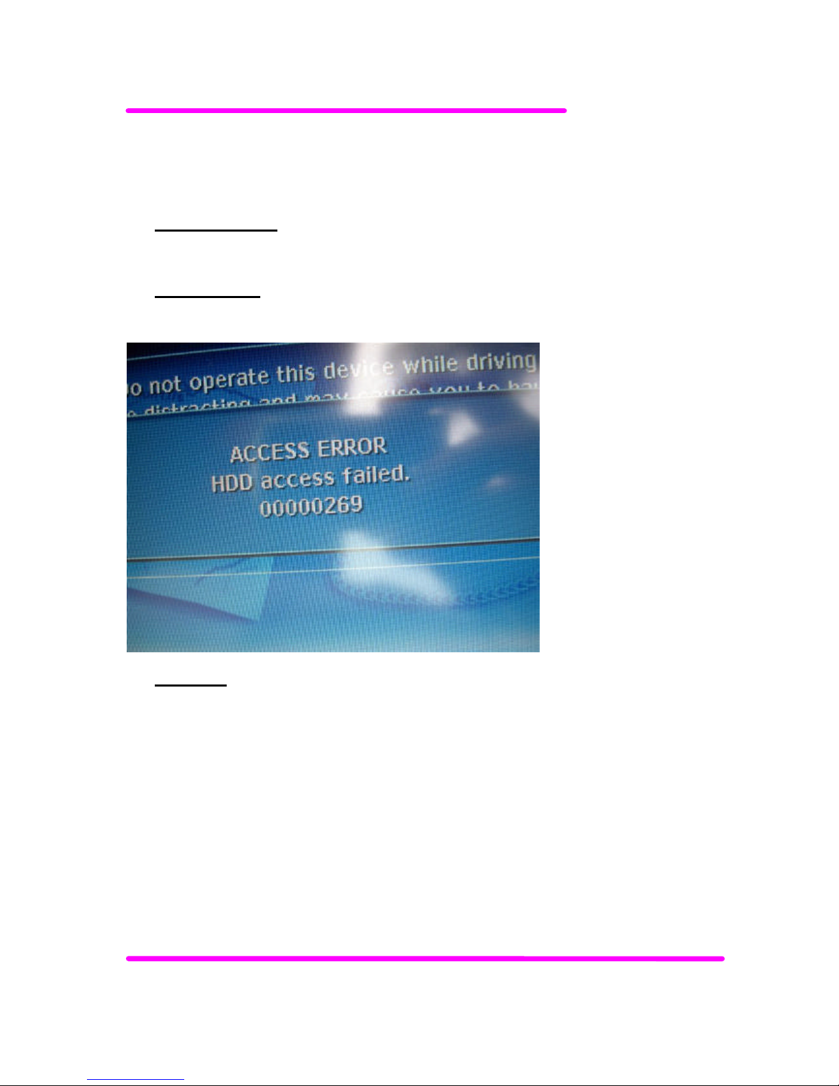
HDD access error message
1) Model outline:
NAX963HD
2) Description:
The navigation shows “ACCESS ERROR” on the display, as shown below.
3) Solution
Reset the NAX963HD navigation unit to the factory setting by following
the below mentioned procedure:
1) Press “Menu” on the main unit.
2) Select “Settings” on the touch screen
3) Press “Next”
4) Select “ Service option”
5) Select “Reset to Factory Settings”
6) Press “OK”, when asked for.
Page 2

Service information
Control no.: 06SI010-R
CLARION Europa GmbH, Hessenring 19-21, 64546 Morfelden-Walldorf, ++49 6105 / 977-0 Fx / 977-100
06SI010-R 10.11.06 Page 2 of 2
Attention:
All user data on the hard drive will be lost and the factory settings will be
installed again.
After the installation of the factory settings, the NAX963HD will start up
automatically.
It may happen that the NAX963HD show this error message again. In this
case, switch off the unit and restart it manually. Now the error message
shall not be shown again.
In case the error message will not disappear, a hardware defect on the
unit is detected and the unit has to be exchanged via CEF.
Page 3
NAX963HD
- 1 -
Service Manual
Published by Service Dept.
Printed in Japan
Clarion Co., Ltd.
50 Kamitoda, Toda-shi, Saitama 335-8511 Japan
Service Dept.: 5-66 Azuma , Kitamoto-shi, Saitama 364-0007 Japan
Tel: +81-48-541-2335 / 2432 FAX: +81-48-541-2703
298-6375-00
AUG.2006
Model
HDD Navigation System
(QY-5000E-A)
SPECIFICATIONS
Navigation System
GPS receiving frequency:
1575.42 MHz, C/A Code
Sensibility: -130 dBm or better
Number of GPS channels:
15 channels
Voice synthesis: ADPCM,
Sampling frequency;11.025 kHz
Power supply voltage: +14V
Ground: Negative
Current consumption: less than 3.0A
Dimensions(mm): 205(W)x29.5(H)x169(D)
GPS aerial
Mode: Microstrip flat aerial
Dimensions(mm): 30.4(W)x11.7(H)x35.5(D)
Impedance: 50 ohm
NOTES
About the hard disk drive
* Data saved to the hard disk drive may get lost in case of
a breakdown, malfunction, or other trouble of this unit.
Importing Data via USB Port
* Data may be broken when using USB memories sticks
in the following situation: When disconnecting the USB
memory stick or turning the power off during writing or
reading data. When affected by static electricity or electric noises.
* Music files (MP3, WMA, etc.) stored in the USB memory
stick cannot be played back.
("Data" : Including the stored locations and their data,
route data, data stored in the Favourite & Frequent List,
setting data set from the Setting menu, and data imported
from the USB memory stick (Wallpapers, Safety Camera locations, etc.)
* The special equipment is necessary to replace IC103.
* We cannot supply PWB with component parts in
principle. When a circuit on PWB has failure, please
repair it by component parts base.
Parts which are not mentioned in service manual are
not supplied.
* Specifications and design are subject to change without
notice for further improvement.
This product is a lead free model.
Lead free solder is used in PWB stamped LF mark.
Please keep the following conditions when you repair.
1. Use lead free solder.
* Koki's lead free solder S3X-55M 0.6mm
(CLARION Parts No.642-0231-01)
* Koki's lead free solder S3X-55M 1.0mm
(CLARION Parts No.642-0231-02)
2. Use a nitrogen solder system.
3. Do not use "General solder" and "Lead free solder"
together.
Page 4
NAX963HD
- 2 -
To engineers in charge of repair or
inspection of our products.
Before repair or inspection, make sure to follow the
instructions so that customers and Engineers in charge
of repair or inspection can avoid suffering any risk or
injury.
1. Use specified parts.
The system uses parts with special safety features against fire
and voltage. Use only parts with equivalent characteristics
when replacing them.
The use of unspecified parts shall be regarded as remodeling
for which we shall not be liable. The onus of product liability
(PL) shall not be our responsibility in cases where an accident
or failure is as a result of unspecified parts being used.
2. Place the parts and wiring back in their original positions after
replacement or re-wiring.
For proper circuit construction, use of insulation tubes, bonding, gaps to PWB, etc, is involved. The wiring connection and
routing to the PWB are specially planned using clamps to keep
away from heated and high voltage parts. Ensure that they are
placed back in their original positions after repair or inspection.
If extended damage is caused due to negligence during repair, the legal responsibility shall be with the repairing company.
3. Check for safety after repair.
Check that the screws, parts and wires are put back securely
in their original position after repair. Ensure for safety reasons
there is no possibility of secondary ploblems around the repaired spots.
If extended damage is caused due to negligence of repair, the
legal responsibility shall be with the repairing company.
4. Caution in removal and making wiring connection to the parts
for the automobile.
Disconnect the battery terminal after turning the ignition key
off. If wrong wiring connections are made with the battery connected, a short circuit and/or fire may occur. If extensive damage is caused due to negligence of repair, the legal responsibility shall be with the repairing company.
5. Cautions in soldering
Please do not spread liquid flux in soldering.
Please do not wash the soldering point after soldering.
6. Cautions in soldering for chip capacitors
Please solder the chip capacitors after pre-heating for replacement because they are very weak to heat.
Please do not heat the chip capacitors with a soldering iron
directly.
7. Cautions in handling for chip parts.
Do not reuse removed chips even when no abnormality is observed in their appearance. Always replace them with new
ones. (The chip parts include resistors, capacitors, diodes, transistors, etc).
Please make an operation test after replacement.
8. Cautions in handling flexible PWB
Before working with a soldering iron, make sure that the iron
tip temperature is around 270 . Take care not to apply the
iron tip repeatedly(more than three times)to the same patterns.
Also take care not to apply the tip with force.
9. Turn the unit OFF during disassembly and parts replacement.
Recheck all work before you apply power to the unit.
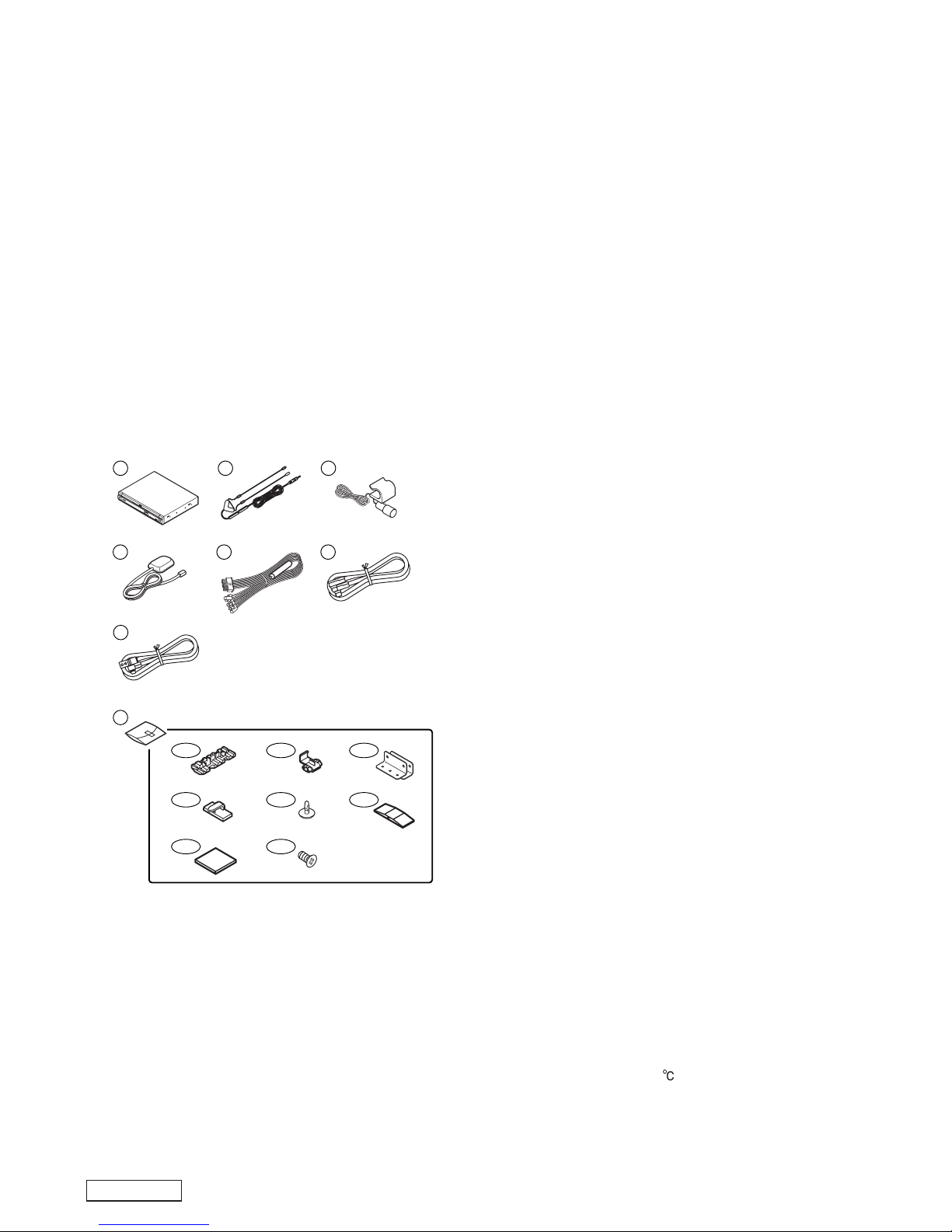
COMPONENTS
QY-5000E-A
1. Main unit ----------- 1
2. RDS-TMC amtenna ZCA-412-310 1
3. Microphone for voice control 081-0034-00 1
4. GPS antenna 096-0147-00 1
5. Power supply lead 854-6451-50 1
(5A Fuse 120-0050-00 1)
6. RGB cable(2.5m) 855-2433-01 1
7. CeNET cable(2.5m) 855-3421-90 1
8. Accessory bag ----------- 1
8-1. Electro-tap(for speed sensor) 060-0018-00 2
8-2. Electro-tap 060-0305-00 1
8-3. Mounting bracket 300-7362-03 2
8-4. Cord holder 321-1026-01 10
8-5. Canoe clip 335-2515-00 4
8-6. Waterproof rubber 345-7473-00 1
8-7. Double-sided tape for fastening the antenna
347-6369-00 1
8-8. Inatallation bolt(M4x6) 714-4006-8B 4
1 2 3
4 5 6
7
8
8-1 8-2 8-3
8-4 8-5 8-6
8-7 8-8
Page 5
NAX963HD
- 3 -
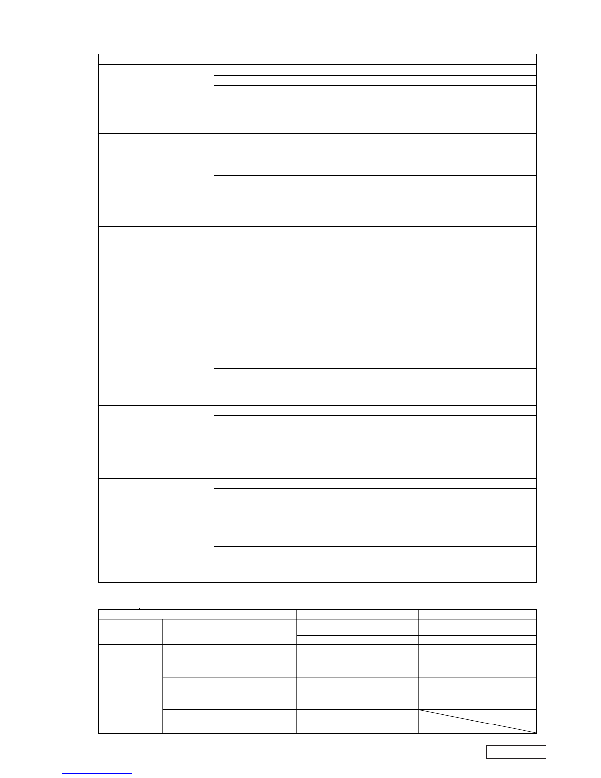
The provider of RDS-TMC is not
automatically selected.
Error Message Cause Remedy
USB memory
device
ACCESS ERROR
The USB memory device cannot be
accessed.
The USB memory is not
connected correctly.
Connect the USB memory again.
The USB memory is not recognised.
Connect another USB memory.
Hard Disk Drive
TEMP ERROR
Cannot operate correctly due to high
temperature. Please wait until
temperature becomes normal again.
The HDD cannot be accessed
because the temperature in the
vehicle is extremely high
Please wait until the temperature
becomes appropriate.
TEMP ERROR
Cannot operate correctly due to low
temperature. Please wait until
temperature becomes normal again.
The HDD cannot be accessed
because the temperature in the
vehicle is extremely low
Please wait until the temperature
becomes appropriate.
ACCESS ERROR
Malfunction occured in the HDD.
Please consult your nearest dealer.
The HDD cannot be accessed.
The sectors or clusters of the
HDD may be damaged.
Problem Check point Remedy
Connection of power cable
Connection of RGB cable
Output of RGB signal
Output level of RGB signal
Dot clock
Connect power cable properly.
Confirm the frequency of the dot clock. (TP534)
Connect RGB cable properly.
Connect microphone properly.
Connect GPS antenna properly.
Connect antenna properly.
Change the installation position.
Separate from the antenna of the vehicle.
(especially, glass antenna)
Connect internal wiring (ANT700,ANT701) properly.
Connect speed pulse cable properly.
Connection of CeNET cable
Connect CeNET cable properly.
Power supply circuit
Confirm the output voltage of the power properly.
TP1000 HDD_5V
TP1001 D_5V
TP1003 D_3.3V
TP1008 DDR_2.5V
TP1004 VCC 1.22V
Confirm the output of RGB signal.
TP1115 R
TP1116 G
TP1114 R
Confirm the output level of RGB signal.
TP1115 R
TP1116 G
TP1114 R
Confirm collector voltage of Q803.
0V : MUTE-ON
3.3V : MUTE-OFF
Confirm IC800.
pin9(SDTO):Data output according to voice input.
pin10(LRCK):11.025KHz
pin11(MCLK):8.46MHz
pin12(SCLK):705KHz
Confirm collector voltage of Q801.
0V : MUTE-ON
3.3V : MUTE-OFF
Confirm audio wave form of TP801(AD_IN).
Confirm an output signal of TP1105(ECC).
Confirm the power supply voltage.
TP2101 R_TU8V
TP2113 TUNER3.2V
Confirm the oscillation of X2102(10MHz)
and output power of TP2209 (BU5V).
Measure pin1(VOUT) of Gyro(IC702) with the
tester. Confirm the voltage.
At geostationary: about 2.5V
When sets are rotatedand: voltage moves.
Confirm IC801.
pin1(LRCK):11.025KHz
pin18(MCLK):8.46MHz
pin19(BCLK):705KHz
pin20(DIN):Data input
Confirm an analog aoudio signal output of pin12 of
IC801.
HDD
Insert HDD, and put protecting.
Adjust the volume properly.
The color of the screen is defective.
Guide voice doesn't sound.
Volume level of guide voice
Clock and data input of DAC(IC801)
Output of DAC(IC801)
MUTE setting
Connection of microphone
Connection of speed pulse
Connection of GPS antenna
Connection of antenna
Setting position of window antenna
Noise source in car (PC,DC/AC converter)
Connection of internal wiring
Wave form of speed pulse
Input signal of ADC(IC800)
Clock and data output of ADC(IC800)
Gyro sensor
Stop the equipment that generates the noise.
Tuner Pack
RDS/TMC microcomputer
Selection of "TMC Provider screen".
Select "Automatic".
Power indicator doesn't light.
(The power supply doesn't enter).
Screen is not displayed.
Map is not displayed.
The car position doesn't move.
GPS reception is defective.
RDS-TMC reception is defective.
Voice recognition is defective.
TROUBLESHOOTING
ERROR MESSAGES
Page 6
NAX963HD
- 4 -
IC403
SRAM
512KB
IC200,IC201,
IC202,IC203
DDR-SDRAM
128MB(256Mbx4)
IC400
DISK ON CHIP
64MB
IC800
ADC
SENSOR
I/F
J1102 J1103 P701
(Connector for production)
IC700
ADC
BL700
GPS
Tuner Pack
J701
IC702
GYRO
SENSOR
J800
MIC
IC803
FILTER
R/G/B
IC401
BUS BUFER
16
64
16
16
IC501
FPGA
CSYNC
IC103
CPU
IC602
BUS
BUFFER
2.5inch 30GB
HARD DISK DRIVE
16
SCIF5
SCIF0
USB Host
ATAPI
RGB
DDR I/FEX-BUS
SSI0
SSI1
CS0
EX_CS0
8
H-UDI
JTAG
IC801
DAC
Control
IR IN
(96MHz)
(32MHz)
IC1102,IC1103
RGB
BUFFER
GUIDE
SIG.
TTS/WAVE (GUIDE VOICE)
VOICE RECOGNITION
16
X101
OSC
48MHz
X100
OSC
14.31818MHz
EXTALDOTCLKIN USBCLKAUDIO_CLK
CLKOUT
(CKIO)
32MHz
- FPGA
- DOC
- DEBUG CN
CLKIN(CKIO)
From SH7770
32MHz
EX_CS2
IC909
MICOM
IC912
IE-BUS
DRIVER
X900
XTAL
10MHz
IC802,IC804
BUFFER
SCIF2
UART
J500(Unmounting)
DEBUG CONNECTOR for Development
X102
OSC
8.46MHz
IC2105
MICOM
RDS-
DEMODURATOR
IC2102
BL2101
RDS/TMC Tuner
C2B
X2102
XTAL
10MHz
X2101
XTAL
4.33MHz
UART
UART
UART
SCIF7
16
EX_CS4
EX_CS7
EX_CS1
From SH7770
32MHz
From SH7770
32MHz
IC908
EEPROM
1Kbit
Note
RDS-TMC PWB Block
Main PWB Block
J1100 J1101
Control signal
Other signal
Video signal
Audio signal
㪧㪸㫉㪸㫃㫃㪼㫃㩷BUS
㪪㪼㫉㫀㪸㫃㩷㪺㫆㫄㫄㫌㫅㫀㪺㪸㫋㫀㫆㫅
CSYNC
TP
IC505
PLL
(9.1101MHz㪄10.085663MHz)
PDOUT4FSCEXCLK
SCIF4
ANT AMP
RDS-TMC
ANT
GPS
ANT
POWER
SUPPLY
BLOCK
Q1100,Q1101,IC1100,IC1101
SENSOR I/F:
PKB,BACK,ECC
B/U
12V
IC502
BUFFER
MIC CON.
CeNET
CONN.
CeNET
CONN.
To RDS
CONNECT.
HDD
CONNECT.
USB
CON.
BU12V, PKB/BACK/ECC
CONNECTOR
RGB
CONNECTOR
SERIAL
CONNECTOR
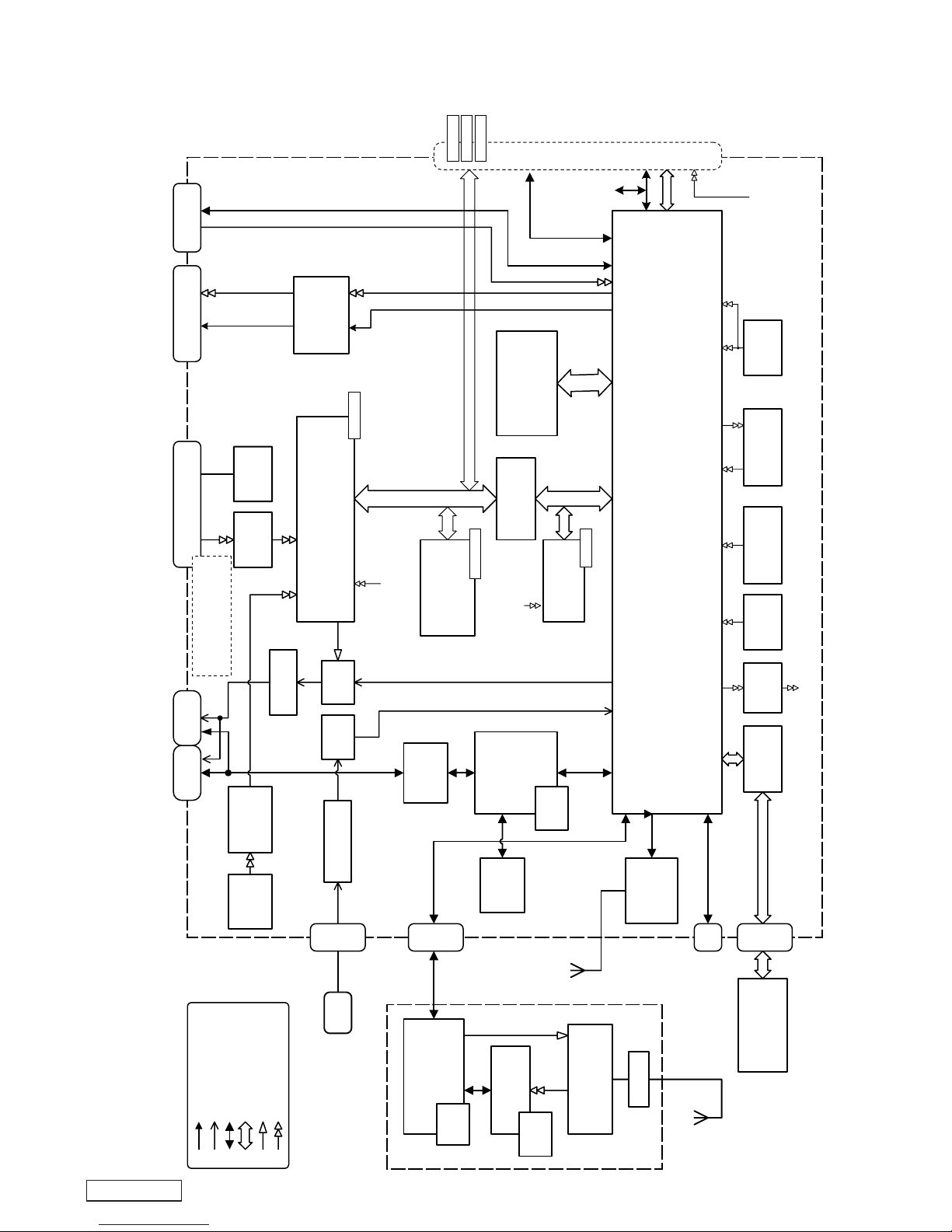
BLOCK DIAGRAM
Video/Audio/Control block
Page 7
NAX963HD
- 5 -
Debug
Connector
Reset Block
IC103
CPU
SH Navi1
/RESET
/RESET_OUT
SRAM
FPGA
HDD
ADC
(AK5357)
IC904
Detector
R3112N211A
IC900
Detector
R3112N211A
IC901
Detector
R3112N211A
HDD_5V DET.
10K
3.9K
3.3K
D_5V
DET VOLT(high):4.81V
DET VOLT(Low):4.58V
0.033uF
100
DDR_2.5V DET.
D_3.3V DET.
DDR
2.5V
0.033uF
100
Disk On Chip
/BUSY
/RSTIN
D_3.3V
D_3.3V
D_3.3V
D_3.3V
D_3.3V
Delay:150ms
1000pF1000pF
/PERI _RESET
47K
D_3.3V
D_5V
1000pF
100
D_3.3V
IC909
SUB
Micon
/RESET
/CPU_RST
100
1000pF
100
10K
/IDE_RST
82
100
/RESET_OUT
/RESET_IN
D_3.3V
100
16K
39K
D_3.3V
0.033uF
100
/NAVI_RESET
100
1000pF
47K
D_3.3V
100
1000pF
SN74ALVC08
(2/4)
SN74ALVC08
(3/4)
SN74ALVC08
(4/4)
SN74ALVC08
47K
10K
10K
/BASE_RESET
/SH_RESET_OUT
/DOC_RST IN
/NAVI_RESET
/DOC_BUSY
1000pF
1000pF
Delay:150ms
Delay:150ms
DET VOLT(high):2.20V
DET VOLT(Low):2.10V
DET VOLT(high):3.11V
DET VOLT(Low):2.96V
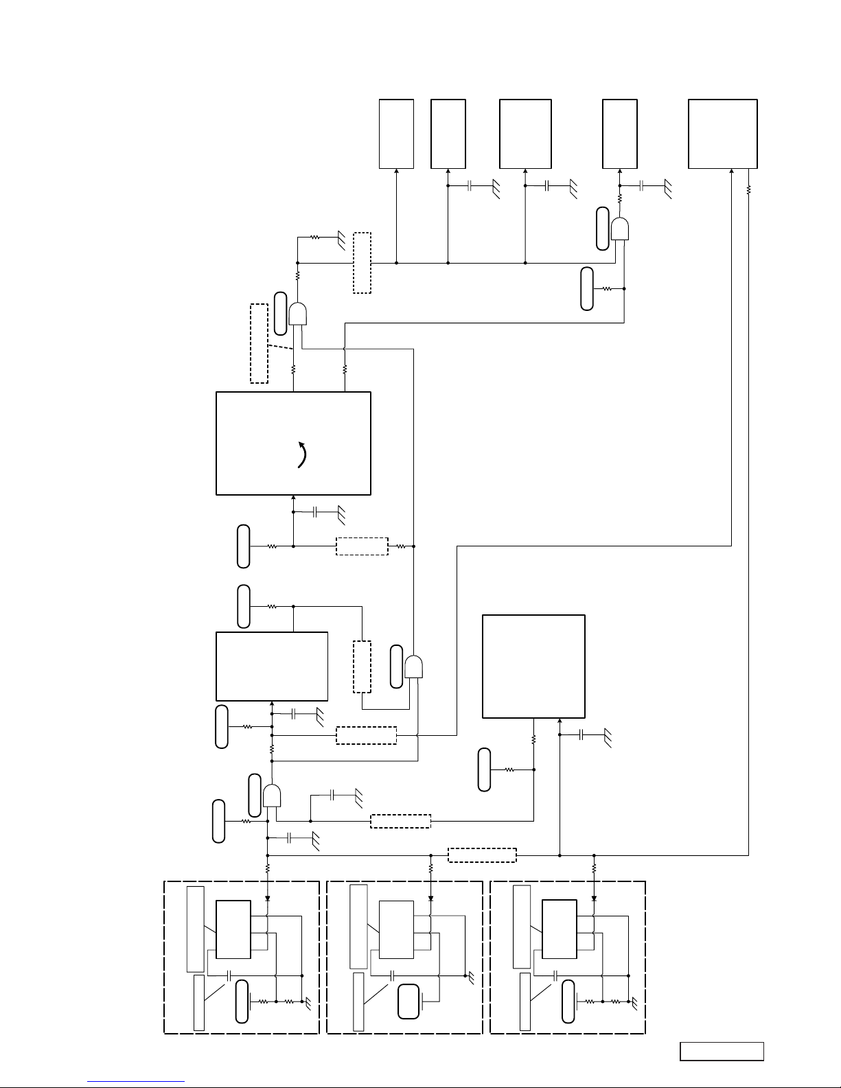
Reset block
Page 8
NAX963HD
- 6 -
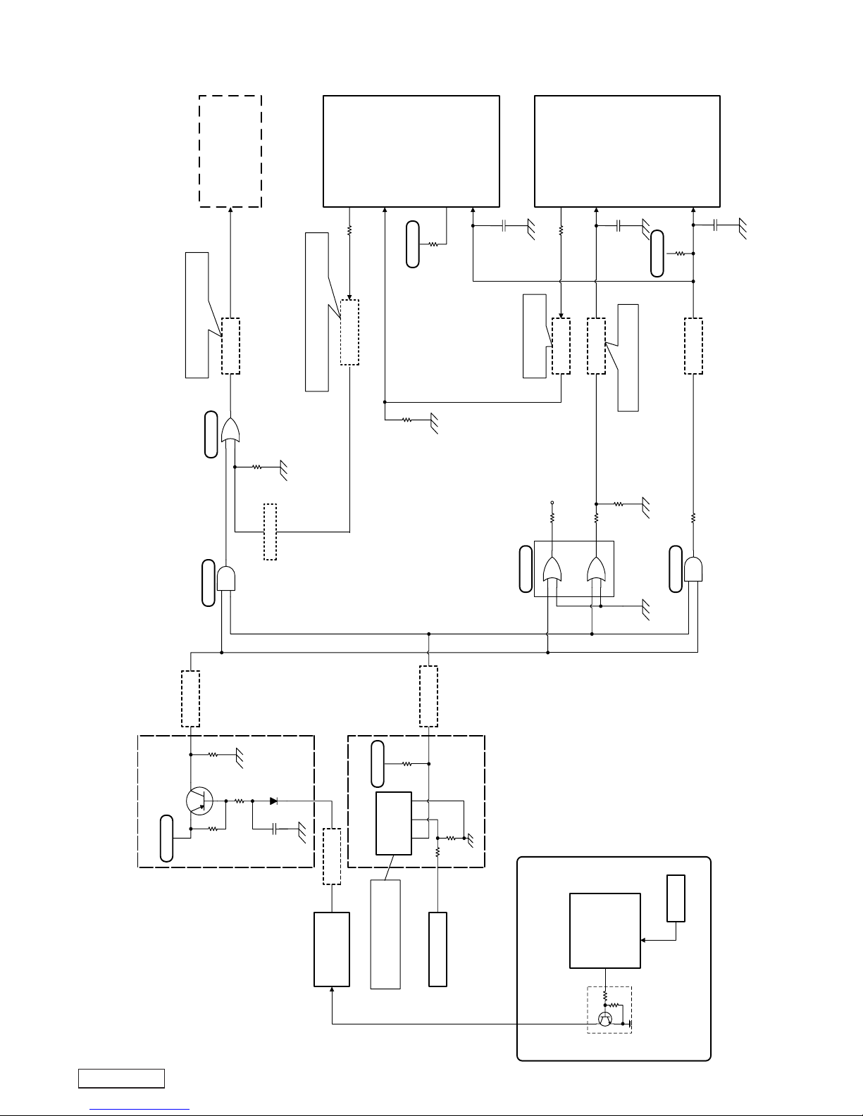
Power Detect Block
Micro
Controller
B/U 12V
IC903
Detector
R3111N271A
ACC_DET
BU_9V_DET
ACC DET.
/SYS-ACC
B/U DET.
/P_OFF
NAVI_PON
/BU-DET
Power supply ON/OFF SW
on Mian PWB
Power-OFF signal
from SH
B/U-VOLT watch signal
to SH
SN74LVC2G32
TC7S32FU
SN74LVC1G08
47K
4.7K
56K
24.7K
47K10K
10K
0.1u
Q900
2SA1586
47K
100
100
B/U_3.3V
B/U_3.3V
B/U_3.3V
B/U_3.3V
D_3.3V
Power supply
(Power circuit block)
B/U
DET. VOLT(high):9.26V
DET. VOLT(Low):8.82V
1SS355
1000pF
100
S-TV
Ce-net
Connector
ACC
IC103
SH-Navi1
NMI
IC909
SUB
Micro
Controller
/SHUTDOWN
100
47K
Shout down signal
by compulsion from microcomputer
1000pF
/P_OFF_B
/NMI_MONI
/SHUTDOWN
/BU_DET
1000pF
NMI
100
D_3.3V
SN74ALVC08(1/4)
GPIO2A20/TX9
GPIO2A22/CSK9
/NAVI_MONI
10K
D_3.3V
10K
D_3.3V
Power detect block
Page 9
NAX963HD
- 7 -
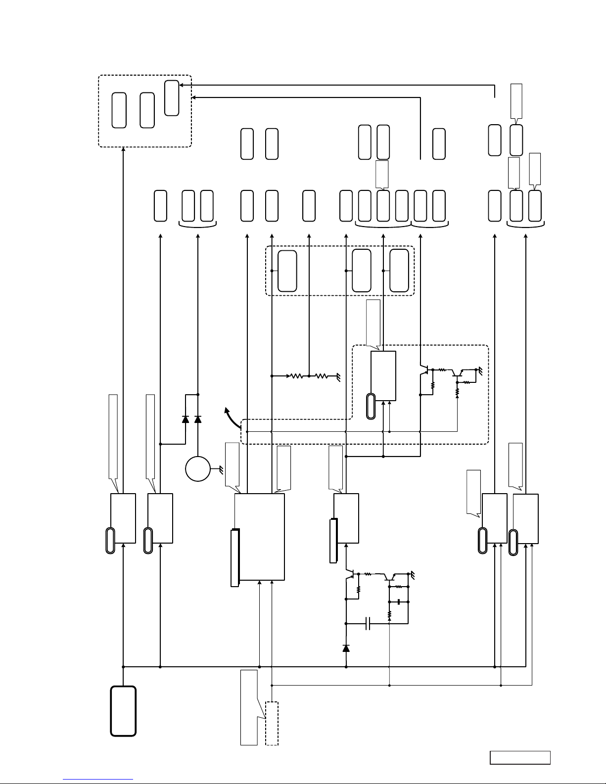
Power circuit block
Power Circuit Block
CAR
BATTERY
IC1002
B/U_5V
TDA3664
Max. permissible current:100mA
Max. permissible current:150mA
Max. permissible
current:3000mA
[D_3.3V] , [D_5V] ON/OFF SW by VCC_1.22V
*
Setting of timing for core power of [Navi core-FPGA] and I/O power.
*
[D_5V] ON/OFF SW for protection of [Navi core] and [FPGA].
IC1000
B/U_3.3V
LM2954
IC1005
VCC_1.22V
DDR_2.5V
TPS5120
IC1003
HDD_5V
LM3485
IC1001 A_9V
BA09CC0WFP
10k
3.9k
10k
2SD1306
2SA2096
4700uF x 2
100(1/4W) x6
RDS PWB
NAVI_P_ON
Detector
2.20V Release
2.10V Det.
Detector
4.81V Release
4.58V Det.
Detector
3.11V Release
2.96V Det.
1.22V
2.5V
IC1006 D_3.3V
BD00KA5WFP
Coin
Battery
DC/DC (200kHz)
DC/DC (100kHz)
Linear
Linear
Linear
IC1004 A_5V
BA05CC0WFP
Vref
Logic
SRAM
GPS
Receiver
SHNavi1 FPGA
SHNavi1 DDR
DDR
HDD
SHNavi1 FPGA
Audio
DAC/ADC
USB
Sub Micon
GPS
Receiver
Gyro
Analog
circuit
Audio
DAC/ADC
Mic
RGB
Encoder
Logic
Max. permissible
current:3000mA
Max. permissible
current:500mA
Max. permissible
current:1000mA
Max. permissible
current:1000mA
Max. permissible
current:3000mA
10k
470
10k
2SC4081
2SB1188
220
Power supply circuit ON/OFF
SW on Navi PWB
RDS/TMC
Tuner
8.5uA typ.
120uA max.
85mA typ.
95mA max.
GPS
Receiver
Tuner
Micon
RDS De-
Modulator
105mA max.
500mA max.
40mA max.
20mA max.
(DataSheet)
13.5mA max.
(DataSheet)
30mA max.
(DataSheet)
30mA max.
(DataSheet)
2.2u
15k
(F)
15k
(F)
Linear
Linear
Page 10

NAX963HD
- 8 -
5A Fuse
(120-0050-00)
Main power supply (Yellow)
Speed sensor (Pink)
Reverse gear signal (Purple/white)
Ground (Black)
NAX963HD
Front view
(inside of Escutcheon)
Rear view
VRX868RVD
GPS antenna
(096-0147-00)
Microphone for voice control
(081-0034-00)
RDS-TMC antenna
(ZCP-412-310)
Power supply lead
(854-6451-50)
RGB cable
(855-2433-01)
CeNET cable
(855-3421-90)
Handbrake (Green)
Connectors
Example of connecting to the VRX868RVD
HDD
1
RDS-TMC antenna recept.
3
1
2
3 4
Mic.jack
6
GPS antenna recept.
8
5
7
8
6
Power supply connector
2468
1357
4
1
2
3
4
5
6
7
8
N.C.
PARKING BRAKE
N.C.
SPEED SENSOR
GROUND
REVERSE SIG.
BATTERY (+)
N.C.
RGB connector
3
7
5
6
8
2
1
4
7
1
2
3
4
5
6
7
8
B
C-SYNC
R
N.C.
N.C.
G
N.C.
N.C.
1234
USB connector
2
1
2
3
4
5V
DD+
GND
CeNET connector
11 12
78910
3456
1132
5
1
2
3
4
5
6
7
8
GND
SYS B/U
L-CH(+)
EXT(+)
EXT(-)
GUS(+)
R-CH(+)
R-CH(-)
9
10
11
12
13
SYS ACC
BUS(-)
L-CH(-)
ILLUMI.
N.C.
WIRE CONNECTION
Page 11

NAX963HD
- 9 -
EXPLANATION OF IC
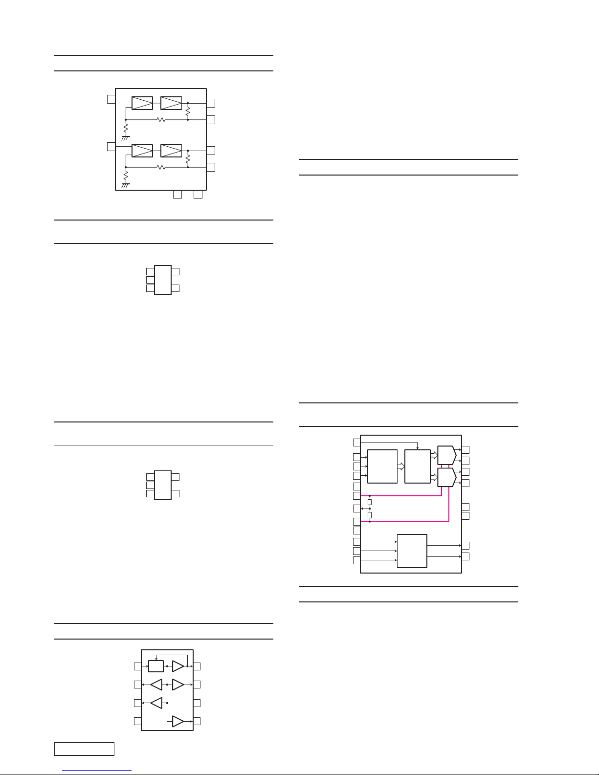
051-3304-90 LP2954IMX Voltage Regulator
Terminal Description
pin 1: Power out : O : DC power voltage output.
pin 2: Sense : IN : The voltage regulator may be pin-strapped
for 5V operation using its internal resistive
divider by tying the Output and Sense pins
together.
pin 3: Shut Down_ : IN : A logic-level signal will shut off the regu-
lator output when aLOW (<1.2V) is
applied to the Shutdown input.
pin 4: Ground : - : Ground.
pin 5: Error_ : O : Error flag output.
pin 6: 5V-TAP : IN : The voltage regulator may be pin-strapped
for 5V operation using its internal resistive
divider by tying the Feedback pin and 5V-
Tap pins together.
pin 7: Feed back : IN : Feed back voltage input.
pin 8: INPUT : IN : Positive power supply input.
051-3356-90 BD00KA5WFP
Positive Voltage Regurator(Adjustable)
051-3377-90 LM3485MM Hysteretic PFET Buck Controller
General Description
The LM3485 is a high efficiency PFET switching regulator controller
that can be used to quickly and easily develop a small, low cost,
switching buck regulator for a wide range of applications.
The hysteretic control architecture provides for simple design without
any control loop stability concerns using a wide variety of external
components.
The PFET architecture also allows for low component count as well
as ultra-low dropout, 100% duty cycle operation.
Another benefit is high efficiency operation at light loads without an
increase in output ripple.
Current limit protection is provided by measuring the voltage across
the PFET's RDS(ON), thus eliminating the need for a sense resistor.
The cycle-by-cycle current limit can be adjusted with a single resistor, ensuring safe operation over a range of output currents.
Terminal Description
pin 1: I SENSE : The current sense input pin. This pin should
be connected to Drain node of the external
PFET.
pin 2: GND : Signal ground.
8
7
6
5
INPUT
FEEDBACK
5V TAP
ERROR_
1
2
3
4
OUTPUT
SENSE
SHUTDOWN_
GROUND
5.
4.
3.
2.
1.
Adjust
Output
N.C.
Vcc
On/Off (H=ON)
FinGround
R1
R2
Vc
Vo
I SENSE
GND
NC
FB
1
2
3
4
V IN
P GATE
PWR GND
ADJ
8
7
6
5
pin 3: NC : No connection.
pin 4: FB : The feedback input. Connect the FB to a
resistor voltage divider between the output
and GND for an adjustable output voltage.
pin 5: ADJ : Current limit threshold adjustment. It con-
nects to an internal 5.5uA current source. A
resistor is connected between this pin and
the input Power Supply. The voltage across
this resistor is compared with the VDS of the
external PFET to determine if an over-current
condition has occurred.
pin 6: PWR GND : Power ground.
pin 7: P GATE : Gate Drive output for the external PFET.
PGATE swings between VIN and VIN-5V.
pin 8: V I N : Power supply input pin.
051-3380-90 TPS5120DBTRG4
Dual output, Two-phase synchronous buck DC/DC controller
Terminal Description
pin 1: INV 1 : IN : Inverting input of CH 1 error amplifier, skip
comparator, and OVP1/UVP1 comparator.
pin 2 : F B 1 : O : Feedback output of CH 1 error amplifier.
pin 3 : SOFT START 1 :I/O: Soft start pin for CH1.
pin 4: PWM/SKIP :IN: PWM/SKIP mode select pin.
pin 5: CT :I/O:External capacitor from CT to GND for
adjusting the triangle oscillator.
pin 6 : 5V STBY : IN : 5V linear regulator output.
pin 7: GND : - : Control ground.
pin 8 : REF : O : 0.85V reference voltage output.
pin 9 : STBY 1 : IN : Standby control for CH1.
pin 10: STBY 2 : IN: Standby control for CH2.
pin 11 : FLT :I/O: Fault latch timer pin.
pin 12 : POWER GOOD : O : Power good open-drain output.
pin 13: SOFT START 2 :I/O: Soft start pin for CH2.
pin 14 : FB 2 : O : Feedback output of CH 2 error amplifier.
pin 15: INV 2 : IN : Inverting input of CH 2 error amplifier, skip
comparator, and OVP2/UVP2 comparator.
pin 16: LH 2 :I/O:Bootstrap capacitor connection for CH2
high-side gate drive.
pin 17: OUT 2u : O : Gate drive output for CH2 high-side
switching FETs.
pin 18: LL 2 :I/O: Bootstrap this pin for CH2 high-side gate
driving return and output current protec-
tion. Connect this pin to the junction of
the high-side FETs for a floating drive
configuration.
pin 19: OUT 2d : O : Gate drive output for CH2 low side gate
drive.
pin 20: OUT GND 2 : - : Ground for CH1 FET drivers.
pin 21: REG 5V IN :IN : External 5V input.
pin 22: Vref 5 : O : 5V internal regulator output.
pin 23: TRIP 2 : IN : External resistor connection for CH2 out-
put current control.
pin 24 : VCC : - : Supply voltage input.
pin 25: TRIP 1 : IN : External resistor connection for CH1 out-
put current control.
pin 26: OUT GND 1 : - : Ground for CH1 FET drivers.
pin 27: OUT 1d : O : Gate drive output for CH1 low side gate
drive.
pin 28: LL 1 :I/O: Bootstrap this pin for CH1 high-side gate
driving return and output current protec-
tion. Connect this pin to the junction of
the high-side FETs for a floating drive
configuration.
pin 29: OUT 1u : O : Gate drive output for CH1 high-side
switching FETs.
pin 30: LH 1 :I/O:Bootstrap capacitor connection for CH1
high-side gate drive.
Page 12
NAX963HD
- 10 -
051-5344-90 NJM2267V-TE2 Dual Video Driver
051-5408-38 R3112N211A-TR-FA
Voltage Drop Detector 2.1V
Terminal description
pin 1: OUTPUT : N channel open drain output.
This terminal will output L, if the voltage of
VDD becomes lower than the setting voltage.
pin 2: VDD : Positive supply voltage.
pin 3: GND : Ground.
pin 4: N.C. : Not in use.
pin 5: C.T. : Delay time capacitor connection.
051-5418-28 R3111N271A-TR-FA
Precision Voltage Down Detector 2.7V
Terminal description
pin 1: OUTPUT : N channel open drain output.
This terminal will output L, if the voltage of
VDD becomes lower than the setting voltage.
pin 2: VDD : Positive supply voltage, negative logic input.
pin 3: GND : Ground.
pin 4: NC : Not in use.
pin 5: NC : Not in use.
051-6650-90 NB2305AT1HDR2G 3.3V Zero Delay Clock Buffer
Terminal Description
pin 1: REF : Input reference frequency, 5 V tolerant input.
pin 2: CLK 2 : Buffered clock output.
pin 3: CLK 1 : Buffered clock output.
pin 4: GND : Ground.
pin 5: CLK 3 : Buffered clock output.
pin 6: VDD : 3.3 V supply.
pin 7: CLK 4 : Buffered clock output.
pin 8: CLK OUT : Buffered clock output, internal feedback on
this pin.
6dB
75ohm Driver
750
ohm
2.0k
ohm
2.2k ohm
1
4
3
6dB
75ohm Driver
750
ohm
2.0k
ohm
2.2k ohm
8
5
6
7 2
GNDVCC
1
2
3
54C.T.
N.C.
OUTPUT
VDD
GND
1
2
3
54N.C.
N.C.
OUTPUT
VDD
GND
CLK OUT
CLK 4
VDD
CLK 3
8
7
6
5
REF
CLK 2
CLK 1
GND
1
2
3
4
PLL
Bit CK IN 19
LR CK IN 1
DATA IN 20
Vref P 5
Vref N 6
V MID 8
Audio
Interface
Digital
Filters
DAC
Vout L P12
Vout L N11
DAC
Vout R P9
Vout R N10
A VDD 4
A GND 7
Serial data IN 14
LATCH IN 13
Serial CK IN 15
Control
Interface
Zero Flag L17
Zero Flag R16
Master Clock 18
D VDD2
D GND3
051-6834-00 XC3S50-4VQG100I-0985 FPGA
Terminal Description
pin 1: A20 : Address input.
pin 2: A19 : Address input.
pin 3: GND : Ground.
pin 4: A18 : Address input.
pin 5: A5 : Address input.
pin 6: VCCO : 3.3V power supply for IC.
pin 7: VCCAUX : 2.5V power supply for AUX.
pin 8: A4 : Address input.
pin 9: A3 : Address input.
pin 10: GND :Ground.
pin 11: A2 : Address input.
pin 12: A1 : Address input.
051-6718-90 AK5357VT-E2 96kHz 24Bit ADC
Terminal Description
pin 1 : A IN R : IN: R channel audio signal input.
pin 2 : A IN L : IN: L channel audio signal input.
pin 3 : CK S 1 : IN: Clock Mode select.
pin 4 : V COMMON : O : Common voltage output = A VDD/2
pin 5: A G ND : - : Analog ground.
pin 6: A VDD : - : Positive voltage supply for analog section.
pin 7 : D VDD : - : Positive voltage supply for digital section.
pin 8: D G ND : - : Digital ground.
pin 9 : SDO : O : Audio Serial data output.
pin 10: LR CK I/O :I/O: Output channel clock. L output in Master
Mode at Power-down mode.
pin 11 : MASTER CLK : IN : Master clock input.
pin 12: S CLK :I/O: Audio Serial data clock input. L output in
Master Mode at Power-down mode.
pin 13: PDN : IN : Power down & reset signal input.
L = Power-down mode.
pin 14 : DIF : IN: Audio interface format.
H = 24bit I2S compatible
L = 24bit MSB justified
pin 15 : CK S 2 : IN: Clock Mode select.
pin 16 : CK S 0 : IN: Clock Mode select.
051-6731-90 WM8718SEDS/R
24 bit Differential Stereo DAC with Volume control
Page 13
NAX963HD
- 11 -
pin 13: D15 : Data input/output.
pin 14: D14 : Data input/output.
pin 15: D13 : Data input/output.
pin 16: D12 : Data input/output.
pin 17: D11 : Data input/output.
pin 18: VCCINT : 1.2V power supply for Core.
pin 19: VCCO :3.3V power supply for IC.
pin 20: GND :Ground.
pin 21: D10 : Data input/output.
pin 22: D9 : Data input/output.
pin 23: D8 : Data input/output.
pin 24: M1 : Configuration mode setting.
pin 25: M0 : Configuration mode setting.
pin 26: M2 : Configuration mode setting.
pin 27: CS_B : For Configuration.
pin 28: RDWR_B : Read/Write signal input.
pin 29: GND :Ground.
pin 30: D7 : Data input/output.
pin 31: VCCO :3.3V power supply for IC.
pin 32: D6 : Data input/output.
pin 33: VCCAUX :2.5V power supply for AUX.
pin 34: D5 : Data input/output.
pin 35: D4 : Data input/output.
pin 36: NC : Not in use.
pin 37: NC : Not in use.
pin 38: N_SH_RDY : Ready signal output for CPU.
pin 39: CKIO : Clock input.
pin 40: NC : Not in use.
pin 41: GND :Ground.
pin 42: INIT_B : For Configuration.
pin 43: D3 : Data input/output.
pin 44: D2 : Data input/output.
pin 45: VCCINT : 1.2V power supply for Core.
pin 46: VCCO :3.3V power supply for IC.
pin 47: D1 : Data input/output.
pin 48: D0 : Data input/output.
pin 49: N_WE1 : Write enable input.
pin 50: N_WE0 : Write enable input.
pin 51: DONE : High output after configuration.
pin 52: CCLK : Configuration clock input.
pin 53: N_RD : Read signal input.
pin 54: N_CS_FPGA : Chip select input.
pin 55: NC : Not in use.
pin 56: GND :Ground.
pin 57: VCCO :3.3V power supply for IC.
pin 58: VCCAUX :2.5V power supply for AUX.
pin 59: NC : Not in use.
pin 60: NC : Not in use.
pin 61: NC : Not in use.
pin 62: N_EIRQ1 : Interrupt signal output for CPU.
pin 63: NC : Not in use.
pin 64: NC : Not in use.
pin 65: VOL_DATA : Data output to Audio-ADC.
pin 66: GND :Ground.
pin 67: VOL_CLK : Clock output to Audio-ADC.
pin 68: VOL_CS :Chip select output to Audio-ADC.
pin 69: VCCINT : 1.2V power supply for Core.
pin 70: VCCO :3.3V power supply for IC.
pin 71: EXTCONT : EXT-AUDIO ON/OFF signal for CeNET.
pin 72: N_MUTE : Audio mute.
pin 73: GND :Ground.
pin 74: N_ILL : Illumination detect.
pin 75: NC : Not in use.
pin 76 : TDO : For JTAG.
pin 77 : TCK : For JTAG.
pin 78 : TMS : For JTAG.
pin 79: GYRO_DATA : Data input from GYRO-ADC.
pin 80: ADC_CLK : Clock output to GYRO-ADC.
pin 81: ADC_CS : Chip select output to GYRO-ADC.
pin 82: GND :Ground.
pin 83: VCCO :3.3V power supply for IC.
pin 84: VCCAUX :2.5V power supply for AUX.
pin 85: PKB : Parking signal input.
pin 86: N_BACK : Back signal input.
pin 87: NC : Not in use.
pin 88: NC : Not in use.
pin 89: NC : Not in use.
pin 90: N_RESETI : Reset input.
pin 91: SPEED_IN : Speed pulse input.
pin 92: NC : Not in use.
pin 93: VCCINT : 1.2V power supply for Core.
pin 94: VCCO :3.3V power supply for IC.
pin 95: GND :Ground.
pin 96: A22 : Address input.
pin 97: A21 : Address input.
pin 98: HSWAP_EN : For Configuration.
pin 99: PROG_B : For Configuration.
pin100: TDI : For JTAG.
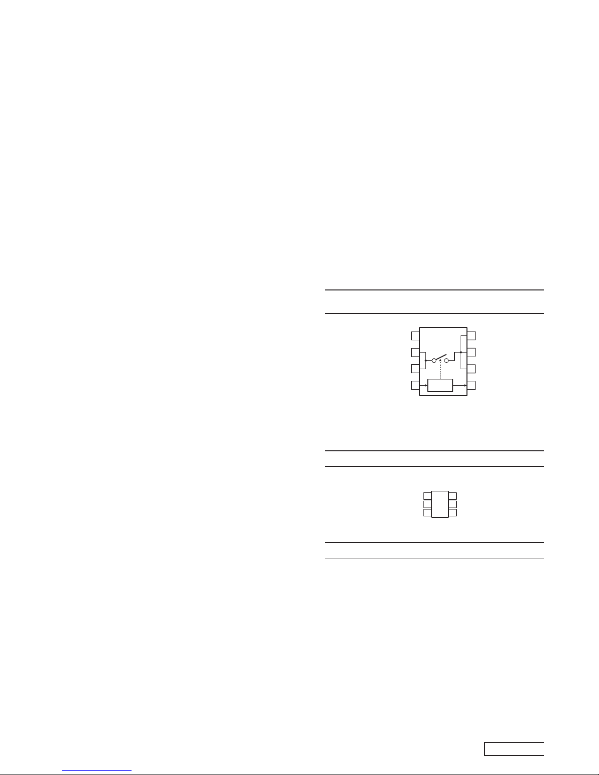
051-6921-90 TPS2041BDGNR
SINGLE, CURRENT-LIMITED, POWER-DISTRIBUTION SWITCH
OC_ ( pin 5 ): Overcurrent and overtemperature false re-
porting, active-low, open-drain output.
051-6923-08 ADCS7476AIMF 1 M SPS 12 bit ADC
051-7289-90 MC74HC4046ADT PLL
Terminal Description
pin 1: PC P OUT : Phase Comparator Pulse Output
pin 2: PC 1 OUT : Phase Comparator 1 Output
pin 3: COMP IN : Comparator Input
pin 4: VCO OUT : VCO Output
pin 5: INH : Inhibit Input
pin 6: C 1 A : Capacitor C1 Connection A
pin 7: C 1 B : Capacitor C1 Connection B
pin 8: GND : Ground (0 V) VSS
pin 9: VCO IN : VCO Input
pin 10 : DEM OUT : Demodulator Output
pin 11: R 1 : Resistor R1 Connection
pin 12: R 2 : Resistor R2 Connection
pin 13 : PC 2 OUT : Phase Comparator 2 Output
pin 14: SIG IN : Signal Input
pin 15 : PC 3 OUT : Phase Comparator 3 Output
pin 16: VCC : Positive Supply Voltage
1
2
3
4
OUT
OUT
OUT
OC_
GND
IN
IN
EN_ ( L = Switch ON )
8
7
6
5
LOGIC
6
5
4
Chip Select input
Serial data output
Clock pulse input
1
2
3
VDD
GND
Analog signal input : Vin
Page 14

NAX963HD
- 12 -
051-7529-90 SN74LVC541APW Octal Bus Buffer
Truth Table
Switch G 1 ( pin 1 ) G 2 ( pin 19 )
OFF H H
OFF H L
OFF L H
ON L L
051-7534-90 SN74LVC1G97DCKR
Configurable Multiple-function Gate
Truth Table
Y IN 2 IN 1 IN 0
L L L L
L L L H
H L H L
H L H H
L H L L
H H L H
L H H L
H H H H
051-7537-90 SN74LVC1G14DCKR
Single Schmitt-Trigger Inverter Gate
051-7539-90 SN74LVC3G34DCTR Triple Buffers
051-7503-78 SN74LVCHR16245AGR 8 x 2 Bus Transceiver
Truth Table
OE_ DIR SW 1 SW 2
L L ON OFF
L H OFF ON
H L OFF OFF
H H OFF OFF
051-7505-08 SN74LV08APWR Quad 2-input AND Gate
051-7505-18 SN74ALVC08PWR Quad 2-input AND Gate
051-7520-08 SN74LVC1G04DCKR Single Inverter
051-7522-08 SN74LVC1G32DCKR Single 2-inputs OR Gate
051-7524-08 SN74LVC1G08DCK Single 2-inputs AND GATE
1 2 3 4 5 6 7 8 9 10 11 12 13 14 15 16 17 18 19 20 21 22 23 24
48
47 46 45 44 43 42 41 40 39 38 37
36 35 34 33 32 31 30 29 28 27 26 25
SW-1SW-2
Logic
SW-1SW-2
Logic
DIR 1
GND
VDD
GND
GND
GND
GND
GND
GND
GND
VDD VDD
VDD
OE 1_
OE 2_DIR 2
14
13
12
11
10
9
8
1
2
3
4
5
6
7
GND
VDD
1
2
3
54VCC
OUT
NC
IN
GND
1
2
3
54VCC
GND
1
2
3
54VCC
GND
20
19
18
17
16
15
14
13
12
11
1
2
3
4
5
6
7
8
9
10
GROUND
G1
VCC
G2
Logic
IN 2
VCC
Y
6
5
4
IN 1
GND
IN 0
1
2
3
IN 0 3
IN 1 1
IN 2 6
Y4
1
2
3
N.C.
GND
54VCC
8
7
6
5
GND
VDD
1
2
3
4
Page 15

NAX963HD
- 13 -
051-7540-90 SN74LVC2G32DCTR Dual 2-input OR Gate
051-9125-60 BS616LV4013EI-70 4 M bit SRAM
Terminal Description
pin 1 : A 4 : IN: Address signal input.
pin 2 : A 3 : IN: Address signal input.
pin 3 : A 2 : IN: Address signal input.
pin 4 : A 1 : IN: Address signal input.
pin 5 : A 0 : IN: Address signal input.
pin 6 : CE_ : IN : Chip enable signal input.
pin 7 : DQ 0 :I/O: The data input / output.
pin 8 : DQ 1 :I/O: The data input / output.
pin 9 : DQ 2 :I/O: The data input / output.
pin 10: DQ 3 :I/O: The data input / output.
pin 11 : VCC : - : Positive supply voltage.
pin 12: GND : - : Ground.
pin 13: DQ 4 :I/O: The data input / output.
pin 14: DQ 5 :I/O: The data input / output.
pin 15: DQ 6 :I/O: The data input / output.
pin 16: DQ 7 :I/O: The data input / output.
pin 17 : WE_ : IN: Write enable signal input.
pin 18 : A 17 : IN : Address signal input.
pin 19 : A 16 : IN : Address signal input.
pin 20 : A 15 : IN : Address signal input.
pin 21 : A 14 : IN : Address signal input.
pin 22 : A 13 : IN : Address signal input.
pin 23 : A 12 : IN : Address signal input.
pin 24 : A 11 : IN : Address signal input.
pin 25 : A 10 : IN : Address signal input.
pin 26 : A 9 : IN: Address signal input.
pin 27 : A 8 : IN: Address signal input.
pin 28: NU : - : Not in use.
pin 29: DQ 8 :I/O: The data input / output.
pin 30: DQ 9 :I/O: The data input / output.
pin 31: DQ 10 :I/O: The data input / output.
pin 32: DQ 11 :I/O: The data input / output.
pin 33 : VCC : - : Positive supply voltage.
pin 34: GND : - : Ground.
pin 35: DQ 12 :I/O: The data input / output.
pin 36: DQ 13 :I/O: The data input / output.
pin 37: DQ 14 :I/O: The data input / output.
pin 38: DQ 15 :I/O: The data input / output.
pin 39 : LB_ : IN : Upper byte control signal input.
pin 40 : UB_ : IN : Lower byte control signal input.
pin 41 : OE_ : IN: Output enable signal input.
pin 42 : A 7 : IN: Address signal input.
pin 43 : A 6 : IN: Address signal input.
pin 44 : A 5 : IN: Address signal input.
Truth Table
CE_ WE_ OE_ LB_ UB_ DQ 0 DQ 8
in in in in in to to
(pin 6) (pin 17) (pin 41) (pin 39) (pin 40) DQ 7 DQ 15
H X X X X high Z high Z
L H H X X high Z high Z
L H L L L output output
L H L H L high Z output
L H L L H output high Z
L L X L L input input
L L X H L X input
L L X L H input X
051-9333-30 MT46V16M16P-6T-IT
256M bit DDR SDRAM (16M words x 16 bits)
Terminal Description
pin 1: VDD : - : Positive voltage supply.
pin 2 : DQ 0 :I/O: Data signal input/output.
pin 3: VDD Q : - : Positive power supply for the data I/O
ports.
pin 4 : DQ 1 :I/O: Data signal input/output.
pin 5 : DQ 2 :I/O: Data signal input/output.
pin 6: VSS Q : - : Ground terminal for the data I/O ports.
pin 7 : DQ 3 :I/O: Data signal input/output.
pin 8 : DQ 4 :I/O: Data signal input/output.
pin 9: VDD Q : - : Positive power supply for the data I/O
ports.
pin 10 : DQ 5 :I/O: Data signal input/output.
pin 11 : DQ 6 :I/O: Data signal input/output.
pin 12: VSS Q : - : Ground terminal for the data I/O ports.
pin 13 : DQ 7 :I/O: Data signal input/output.
pin 14: NU : - : Not in use.
pin 15: VDD Q : - : Positive power supply for the data I/O
ports.
pin 16: Lower DQ S :I/O: Read data strobe output / Write data
strobe input.
pin 17: NU : - : Not in use.
pin 18 : VDD : - : Positive voltage supply.
pin 19: NU : - : Not in use.
pin 20: Lower DM : IN : When this pin is High, the data input are
masked.
pin 21 : WE : IN: Write enable signal input.
pin 22 : CAS :IN : Column address strobe input.
pin 23 : RAS : IN : Row address strobe input.
pin 24 : CS IN :IN : The chip select command input.
pin 25: NU : - : Not in use.
pin 26 : BA 0 : IN : Bank address input.
pin 27 : BA 1 : IN : Bank address input.
pin 28: A10(AP) :IN : Address signal input.
pin 29 : A 0 :IN : Address signal input.
pin 30 : A 1 :IN : Address signal input.
pin 31 : A 2 :IN : Address signal input.
pin 32 : A 3 :IN : Address signal input.
pin 33 : VDD : - : Positive voltage supply.
pin 34 : VSS : - : Negative voltage supply.
pin 35 : A 4 :IN : Address signal input.
pin 36 : A 5 :IN : Address signal input.
pin 37 : A 6 :IN : Address signal input.
pin 38 : A 7 :IN : Address signal input.
pin 39 : A 8 :IN : Address signal input.
pin 40 : A 9 :IN : Address signal input.
pin 41 : A 11 : IN : Address signal input.
pin 42 : A 12 : IN : Address signal input.
pin 43: NU : - : Not in use.
pin 44 : CKE :IN : Clock enable signal input.
pin 45 : CK : IN : Master clock input.
pin 46 : /CK : IN : Master clock input.
pin 47: Upper DM : IN : When this pin is High, the data input are
8
7
6
5
1
2
3
4
GROUND
VDD
Page 16

NAX963HD
- 14 -
masked.
pin 48 : VSS : - : Negative voltage supply.
pin 49 : Vref : - : Reference voltage.
pin 50: NU : - : Not in use.
pin 51: Upper DQ S :I/O: Read data strobe output / Write data
strobe input.
pin 52: VSS Q : - : Ground terminal for the data I/O ports.
pin 53: NU : - : Not in use.
pin 54 : DQ 8 :I/O: Data signal input/output.
pin 55: VDD Q : - : Positive power supply for the data I/O
ports.
pin 56 : DQ 9 :I/O: Data signal input/output.
pin 57 : DQ 10 :I/O: Data signal input/output.
pin 58: VSS Q : - : Ground terminal for the data I/O ports.
pin 59 : DQ 11 :I/O: Data signal input/output.
pin 60 : DQ 12 :I/O: Data signal input/output.
pin 61: VDD Q : - : Positive power supply for the data I/O
ports.
pin 62 : DQ 13 :I/O: Data signal input/output.
pin 63 : DQ 14 :I/O: Data signal input/output.
pin 64: VSS Q : - : Ground terminal for the data I/O ports.
pin 65 : DQ 15 :I/O: Data signal input/output.
pin 66 : VSS : - : Negative voltage supply.
IC103 R8A77700ADA01BGV
RISC Microcomputer for QY5000EA
Terminal Description
pin 1: VSSQ25 : DDR ground
pin 2: VCCQ25 :DDR 2.5V power supply
pin 3: DSA[6] : DDR-SDRAM address output
pin 4: DSA[4] : DDR-SDRAM address output
pin 5: DSA[2] : DDR-SDRAM address output
pin 6: DSA[0] : DDR-SDRAM address output
pin 7: DSRAS# : DDR-SDRAM row address select output
pin 8: DSCAS# : DDR-SDRAM column address select out-
put
pin 9: DSDQ[36] : DDR-SDRAM data input/output
pin 10: DSDM[4] : DDR-SDRAM data select output
pin 11: DSDQ[39] : DDR-SDRAM data input/output
pin 12: DSDQ[45] : DDR-SDRAM data input/output
pin 13: DSDM[5] : DDR-SDRAM data select output
pin 14: DSDQ[46] : DDR-SDRAM data input/output
pin 15: DSDQ[52] : DDR-SDRAM data input/output
pin 16: DSDM[6] : DDR-SDRAM data select output
pin 17: DSDQ[55] : DDR-SDRAM data input/output
pin 18: DSDQ[61] : DDR-SDRAM data input/output
pin 19: DSDM[7] : DDR-SDRAM data select output
pin 20: DSDQ[63] : DDR-SDRAM data input/output
pin 21: TX0/MD[2] : In the reset operation, this port is CPU
setting input. At usually operation, this
port is serial data output to GPS receiv-
er.
pin 22: TX1/MD[3] : In the reset operation, this port is CPU
setting input. At usually operation, this
port is not in use.
pin 23: TX3/IrDA-TX/MD[5] : In t he reset operation, this port is CPU
setting input. At usually operation, this
port is not in use.
pin 24: TX5/HSPI0_CLK : Serial data output to RDS microcomput-
er.
pin 25: NU : Not in use.
pin 26: NU : Not in use.
pin 27: NU : Not in use.
pin 28: NU : Not in use.
pin 29: VSSDLL : DLL ground
pin 30: VDDPLL1 : PLL 1.25V power supply
pin 31: VSSPLL1 : PLL ground
pin 32: VCCQ25 : DDR 2.5V power supply
pin 33: VSSQ25 : DDR ground
pin 34: VCCQ25 :DDR 2.5V power supply
pin 35: DSA[7] : DDR-SDRAM address output
pin 36: DSA[3] : DDR-SDRAM address output
pin 37: DSA[1] : DDR-SDRAM address output
pin 38: DSBA[0] : DDR-SDRAM bank address output
pin 39: /DSWE : DDR-SDRAM write enable.
pin 40: DSDQ[32] : DDR-SDRAM data input/output
pin 41: DSDQS[4] : DDR-SDRAM data input/output
pin 42: DSDQ[35] : DDR-SDRAM data input/output
pin 43: DSDQ[41] : DDR-SDRAM data input/output
pin 44: DSDQS[5] : DDR-SDRAM data strobe input/output
pin 45: DSDQ[42] : DDR-SDRAM data input/output
pin 46: DSDQ[48] : DDR-SDRAM data input/output
pin 47: DSDQS[6] : DDR-SDRAM data strobe input/output
pin 48: DSDQ[51] : DDR-SDRAM data input/output
pin 49: DSDQ[57] : DDR-SDRAM data input/output
pin 50: DSDQS[7] : DDR-SDRAM data strobe input/output
pin 51: DSDQ[59] : DDR-SDRAM data input/output
pin 52 : RX0 : GPS serial data input
pin 53: NU : Not in use.
pin 54: NU : Not in use.
pin 55: RX 5/HSPI0_CS# : Serial data input from RDS microcomput-
er.
pin 56: NU : Not in use.
pin 57: NU : Not in use.
pin 58: NU : Not in use.
pin 59: TX6/MD[10] : In the reset o peration, this por t is CPU
setting input. At usually operation, this
port is not in use.
pin 60: VDDDLL : DLL 1.25V power supply
pin 61: VDDPLL2 : PLL 1.25V power supply
pin 62: VSSPLL2 : PLL ground
pin 63: VCCQ25 :DDR 2.5V power supply
pin 64: VCCQ25 :DDR 2.5V power supply
pin 65: VSSQ25 : DDR ground
pin 66: VCCQ25 :DDR 2.5V power supply
pin 67: DSA[5] : DDR-SDRAM address output
pin 68: DSBA[1] : DDR-SDRAM bank address output
pin 69: VSSQ25 : DDR ground
pin 70: NU : Not in use.
pin 71: DSDQ[37] : DDR-SDRAM data input/output
pin 72: DSDQ[38] : DDR-SDRAM data input/output
pin 73: DSDQ[44] : DDR-SDRAM data input/output
pin 74: VCCQ25 :DDR 2.5V power supply
pin 75: VSSQ25 : DDR ground
pin 76: DSDQ[47] : DDR-SDRAM data input/output
pin 77: DSDQ[53] : DDR-SDRAM data input/output
pin 78: DSDQ[54] : DDR-SDRAM data input/output
pin 79: DSDQ[60] : DDR-SDRAM data input/output
pin 80: VCCQ25 :DDR 2.5V power supply
pin 81: DSDQ[62] : DDR-SDRAM data input/output
pin 82: NU : Not in use.
pin 83: VSSQ25 : DDR ground
pin 84: TX2/MD[4] : In the reset operatio n, this port is CPU
setting input. At usually operation, this
port is serial data output.
pin 85: TX4/HSPI0_TX : Serial data output
pin 86: TX7/HSPI1_TX : Serial data output to sub-microcomputer
Page 17

NAX963HD
- 15 -
pin 87: NU : Not in use.
pin 88: TX9/GPIO_2A20 :Used as GPIO. /P_OFF
pin 89: NU : Not in use.
pin 90: VSSQ : I/O power ground
pin 91: VCCQ :I/O 3.3V power supply
pin 92: VCCQ :I/O 3.3V power supply
pin 93: EXTAL : External clock input (48MHz)
pin 94: DSCK# : DDR-SDRAM clock output (inverted)
pin 95: DSCAP : DDR-SDRAM controller CAP
pin 96: VCCQ25 :DDR 2.5V power supply
pin 97: VSSQ25 : DDR ground
pin 98: VCCQ25 :DDR 2.5V power supply
pin 99: DSA[10] : DDR-SDRAM address output
pin100:VSSQ25 : DDR ground
pin101: DSCS# :DDR-SDRAM area space selection
pin102: DSDQ[33] : DDR-SDRAM data input/output
pin103: DSDQ[34] : DDR-SDRAM data input/output
pin104: DSDQ[40] : DDR-SDRAM data input/output
pin105: VCCQ25 :DDR 2.5V power supply
pin106:VSSQ25 : DDR ground
pin107: DSDQ[43] : DDR-SDRAM data input/output
pin108: DSDQ[49] : DDR-SDRAM data input/output
pin109: DSDQ[50] : DDR-SDRAM data input/output
pin110: DSDQ[56] : DDR-SDRAM data input/output
pin111: VCCQ25 :DDR 2.5V power supply
pin112: DSDQ[58] : DDR-SDRAM data input/output
pin113: NU : Not in use.
pin114:VSSQ25 : DDR ground
pin115: RX2 : Serial data input
pin116: RX4/HSPI0_RX : Serial data input
pin117:RX7/HSPI1_RX : Serial data input from sub-microcomput-
er
pin118: NU : Not in use.
pin119: RX9/GPIO_2A21 : Used as GPIO. /BU_DET
pin120: VSSQ : I/O power ground
pin121: VCCQ : I/O 3.3V power supply
pin122: VSSQ : I/O power ground
pin123: VSSQ : I/O power ground
pin124:XTAL : CPU crystal connection
pin125:DSCK : DDR-SDRAM clock output
pin126: NU : Not in use.
pin127: VCCQ25 :DDR 2.5V power supply
pin128: VCCQ25 :DDR 2.5V power supply
pin129:VSSQ25 : DDR ground
pin130: VCCQ25 :DDR 2.5V power supply
pin131:VSSQ25 : DDR ground
pin132: VCCQ25 :DDR 2.5V power supply
pin133:VSSQ25 : DDR ground
pin134: VDD : Core 1.25V power supply
pin135:VSS : Core power ground
pin136: VCCQ25 :DDR 2.5V power supply
pin137:VSSQ25 : DDR ground
pin138: VCCQ25 :DDR 2.5V power supply
pin139:VSSQ25 : DDR ground
pin140: VDD : Core 1.25V power supply
pin141:VSS : Core power ground
pin142: VCCQ25 :DDR 2.5V power supply
pin143:VSSQ25 : DDR ground
pin144: VDD : Core 1.25V power supply
pin145:VSSQ25 : DDR ground
pin146:VSS : Core power ground
pin147: VSSQ : I/O power ground
pin148: VCCQ : I/O 3.3V power supply
pin149: VCCQ : I/O 3.3V power supply
pin150: VSSQ : I/O power ground
pin151: VCCQ : I/O 3.3V power supply
pin152: VSSQ : I/O power ground
pin153:TRST# :H-UDI reset input
pin154: NU : Not in use.
pin155: NU : Not in use.
pin156:DSA[11] : DDR-SDRAM address output
pin157:DSA[12] : DDR-SDRAM address output
pin158:DSA[8] : DDR-SDRAM address output
pin159:DSA[9] : DDR-SDRAM address output
pin160: VCCQ25 :DDR 2.5V power supply
pin161: VSSQ : I/O power ground
pin162: TMS : H-UDI mode input
pin163: TDI : H-UDI data input
pin164: TDO : H-UDI data output
pin165: TCK : H-UDI clock input
pin166: DSCKE : DDR-SDRAM clock output enable
pin167: NU : Not in use.
pin168:DSA[13] : DDR-SDRAM address output
pin169:VSSQ25 : DDR ground
pin170:VSSQ25 : DDR ground
pin171: VCCQ : I/O 3.3V power supply
pin172: NU : Not in use.
pin173: NU : Not in use.
pin174: NU : Not in use.
pin175: NU : Not in use.
pin176: DSDQ[30] : DDR-SDRAM data input/output
pin177: DSDQ[26] : DDR-SDRAM data input/output
pin178: DSDQ[31] : DDR-SDRAM data input/output
pin179: DSDQ[27] : DDR-SDRAM data input/output
pin180: VDD : Core 1.25V power supply
pin181:VSS : Core power ground
pin182: NU : Not in use.
pin182: NU : Not in use.
pin184: ASEBRK# :Emulator input/output( brake,
acknowledge)
pin185: NU : Not in use.
pin186: DSDQ[29] : DDR-SDRAM data input/output
pin187: DSDQ[25] : DDR-SDRAM data input/output
pin188: DSDM[3] : DDR-SDRAM data select output
pin189: DSDQS[3] : DDR-SDRAM data input/output
pin190:VSS : Core power ground
pin191: VDD : Core 1.25V power supply
pin192: NU : Not in use.
pin193: NU : Not in use.
pin194: NU : Not in use.
pin195: NU : Not in use.
pin196: DSDQ[23] : DDR-SDRAM data input/output
pin197: DSDQ[19] : DDR-SDRAM data input/output
pin198: DSDQ[28] : DDR-SDRAM data input/output
pin199: DSDQ[24] : DDR-SDRAM data input/output
pin200: VCCQ25 :DDR 2.5V power supply
pin201:VSS : Core power ground
pin202: NU : Not in use.
pin203: NU : Not in use.
pin204: NU : Not in use.
pin205: NU : Not in use.
pin206: DSDM[2] : DDR-SDRAM data select output
Page 18

NAX963HD
- 16 -
pin207:DSDQS[2] : DDR-SDRAM data strobe input/output
pin208: DSDQ[22] : DDR-SDRAM data input/output
pin209: DSDQ[18] : DDR-SDRAM data input/output
pin210:VSSQ25 : DDR ground
pin211: VDD : Core 1.25V power supply
pin212: NU : Not in use.
pin213: NU : Not in use.
pin214: NU : Not in use.
pin215: NU : Not in use.
pin216: DSDQ[20] : DDR-SDRAM data input/output
pin217: DSDQ[16] : DDR-SDRAM data input/output
pin218: DSDQ[21] : DDR-SDRAM data input/output
pin219: DSDQ[17] : DDR-SDRAM data input/output
pin220: VDD : Core 1.25V power supply
pin221: VSSQ : I/O power ground
pin222: SPDIF_IN : Extended GPIO data latch output
pin223: SPDIF_OUT : FPGA PROG_B output
pin224: NU : Not in use.
pin225: NU : Not in use.
pin226: DSDQ[14] : DDR-SDRAM data input/output
pin227: DSDQ[10] : DDR-SDRAM data input/output
pin228: DSDQ[15] : DDR-SDRAM data input/output
pin229: DSDQ[11] : DDR-SDRAM data input/output
pin230:VSS : Core power ground
pin231: VCCQ : I/O 3.3V power supply
pin232: SSI_SDATA 1 : Data output to DAC for guide signal
pin233:SSI_SDATA0 : The data input from ADC for microphone
pin234: NU : Not in use.
pin235:AUDIO_CLK :Audio clock input for SSI module
(8.46MHz)
pin236: DSDM[1] : DDR-SDRAM data select output
pin237: DSDQS[1] : DDR-SDRAM data strobe input/output
pin238:VSSQ25 : DDR ground
pin239:VSSQ25 : DDR ground
pin240:VSSQ25 : DDR ground
pin241:VSS : Core power ground
pin242:SSI_WS0 : LR clock input
pin243: SSI_SCK0 :Serial bit clock input
pin244: SSI_WS1/HAC_RES#
: LR clock input
pin245: SSI_SCK1 :Serial bit clock input
pin246: DSDQ[12] : DDR-SDRAM data input/output
pin247: DSDQ[8] : DDR-SDRAM data input/output
pin248: DSDQ[13] : DDR-SDRAM data input/output
pin249: DSDQ[9] : DDR-SDRAM data input/output
pin250:VSSQ25 : DDR ground
pin251:VSS : Core power ground
pin252: NU : Not in use.
pin253: NU : Not in use.
pin254: NU : Not in use.
pin255: NU : Not in use.
pin256: DSDQ[6] : DDR-SDRAM data input/output
pin257: DSDQ[2] : DDR-SDRAM data input/output
pin258: DSDQ[7] : DDR-SDRAM data input/output
pin259: DSDQ[3] : DDR-SDRAM data input/output
pin260: VCCQ25 :DDR 2.5V power supply
pin261: VSSQ : I/O power ground
pin262:IDED[7] : IDE data input/output
pin263:IDED[8] : IDE data input/output
pin264: IDERST# : IDE reset output
pin265: DIRECTION : IDE bus buffer direction control output
pin266: DSDQ[5] : DDR-SDRAM data input/output
pin267: DSDQ[1] : DDR-SDRAM data input/output
pin268: DSDM[0] : DDR-SDRAM data select output
pin269: DSDQS[0] : DDR-SDRAM data strobe input/output
pin270:VSSQ25 : DDR ground
pin271: VCCQ : I/O 3.3V power supply
pin272:IDED[5] : IDE data input/output
pin273: IDED[10] : IDE data input/output
pin274:IDED[6] : IDE data input/output
pin275:IDED[9] : IDE data input/output
pin276: DSDQ[4] : DDR-SDRAM data input/output
pin277: DSDQ[0] : DDR-SDRAM data input/output
pin278: VCCQ25 :DDR 2.5V power supply
pin279: VCCQ25 :DDR 2.5V power supply
pin280: VCCQ25 :DDR 2.5V power supply
pin281: VDD : Core 1.25V power supply
pin282:IDED[3] : IDE data input/output
pin283: IDED[12] : IDE data input/output
pin284:IDED[4] : IDE data input/output
pin285: IDED[11] : IDE data input/output
pin286:DSVREF : DDR-SDRAM reference voltage input
pin287: VSS : Core power ground
pin288: VSS : Core power ground
pin289: VSS : Core power ground
pin290: VSS : Core power ground
pin291: VSS : Core power ground
pin292:IDED[1] : IDE data input/output
pin293: IDED[14] : IDE data input/output
pin294:IDED[2] : IDE data input/output
pin295: IDED[13] : IDE data input/output
pin296: VDD : Core 1.25V power supply
pin297: VDD : Core 1.25V power supply
pin298: VDD : Core 1.25V power supply
pin299: VDD : Core 1.25V power supply
pin300: VDD : Core 1.25V power supply
pin301: VCCQ : I/O 3.3V power supply
pin302: IDEIOWR# :IDE disk write output
pin303: IODREQ : IDE-DMA request input
pin304:IDED[0] : IDE data input/output
pin305: IDED[15] : IDE data input/output
pin306: NU : Not in use.
pin307: NU : Not in use.
pin308: VSS : Core power ground
pin309: VSS : Core power ground
pin310: VSS : Core power ground
pin311: VSSQ : I/O power ground
pin312: IDEINT : IDE interrupt request input
pin313: IODACK# : IDE-DMA acknowledge output
pin314: IDEIORDY : IDE ready input
pin315:IDEIORD# : IDE disk resd output
pin316:NMI# : NMI
pin317:IRQ#[4]/EX_CS#[6] : Interrupt input
pin318: IRQ#[5]/EX_CS#[7] : Chip select output
pin319: IRQ#[1]/EX_WAIT[1]
: Interrupt input
pin320: VDD : Core 1.25V power supply
pin321: VDD : Core 1.25V power supply
pin322: IDECS#[0] :IDE chip select output
pin323:IDEA[2] : IDE address output
pin324:IDEA[0] : IDE address output
pin325:IDEA[1] : IDE address output
Page 19

NAX963HD
- 17 -
pin326: NU : Not in use.
pin327:IRQ#[0] : Interrupt input
pin328: NU : Not in use.
pin329: NU : Not in use.
pin330: VSSQ : I/O power ground
pin331:VSS : Core power ground
pin332: NU : Not in use.
pin333: NU : Not in use.
pin334: NU : Not in use.
pin335: IDECS#[1] :IDE chip select output
pin336: NU : Not in use.
pin337: NU : Not in use.
pin338: NU : Not in use.
pin339: NU : Not in use.
pin340: VCCQ : I/O 3.3V power supply
pin341: VDD : Core 1.25V power supply
pin342: GPIO-3-A27 : LED1 control signal output to sub-micro-
computer
pin343: GPIO-3-A28 : LED2 control signal output to sub-micro-
computer
pin344: IRREC : Remote control input
pin346: NU : Not in use.
pin347: NU : Not in use.
pin348: NU : Not in use.
pin349: NU : Not in use.
pin350: VSSQ : I/O power ground
pin351:VSS : Core power ground
pin352: VSSRTC : RTC ground
pin353: NU : Not in use.
pin354: RESOUT# : Reset output
pin355: RESET# : Reset input
pin355: RESET# : Reset input
pin356: NU : Not in use.
pin357: NU : Not in use.
pin358: NU : Not in use.
pin359: NU : Not in use.
pin360: VCCQ : I/O 3.3V power supply
pin361: VCCQ : I/O 3.3V power supply
pin362: NU : Not in use.
pin363: NU : Not in use.
pin364: NU : Not in use.
pin365: NU : Not in use.
pin366: NU : Not in use.
pin367: NU : Not in use.
pin368: EX_CS#[4]/EXCPU_IRQ#
: Chip select output
pin369: VCCQ : I/O 3.3V power supply
pin370: VSSQ : I/O power ground
pin371: VCCQ : I/O 3.3V power supply
pin372: VSSQ : I/O power ground
pin373: VCCQ : I/O 3.3V power supply
pin374: VSSQ : I/O power ground
pin375: VCCQ : I/O 3.3V power supply
pin376:VSS : Core power ground
pin377: VDD : Core 1.25V power supply
pin378: VSSQ : I/O power ground
pin379: VCCQ : I/O 3.3V power supply
pin380: VSSQ : I/O power ground
pin381: VCCQ : I/O 3.3V power supply
pin382:VSS : Core power ground
pin383: VDD : Core 1.25V power supply
pin384: VSSQ : I/O power ground
pin385: VCCQ : I/O 3.3V power supply
pin386: VSSQ : I/O power ground
pin387: VCCQ : I/O 3.3V power supply
pin388: VSS : Core power ground
pin389: VDD : Core 1.25V power supply
pin390: VSSQ : I/O power ground
pin391: VCCQ : I/O 3.3V power supply
pin392: VSSQ : I/O power ground
pin393: VCCQ : I/O 3.3V power supply
pin394:VCCRTC :RTC power supply 3.3V
pin395: NU : Not in use.
pin396: NU : Not in use.
pin397: WE#[2] : EXBUS write enable output
pin398: WE#[3] : EXBUS write enable output
pin399: VCCQ : I/O 3.3V power supply
pin400: VSSQ : I/O power ground
pin401: VCCQ : I/O 3.3V power supply
pin402:D[4] : EXBUS data input/output
pin403:D[0] : EXBUS data input/output
pin404: WE#[1] : EXBUS write enable output
pin405:EX_CS#[1] : EXBUS extended area chip select output
pin406: RD/WR# : EXBUS read/write
pin407: NU : Not in use.
pin408: NU : Not in use.
pin409: NU : Not in use.
pin410: A[3] : EXBUS Address output.
pin411: A[7] : EXBUS Address output.
pin412: A[8] : EXBUS Address output.
pin413: A[15] : EXBUS Address output.
pin414: A[19] : EXBUS Address output.
pin415: A[23] : EXBUS Address output.
pin416: NU : Not in use.
pin417: VSSQ : I/O power ground
pin418: VCCQ : I/O 3.3V power supply
pin419: NU : Not in use.
pin420: NU : Not in use.
pin421: GPIO-3-A25 : PLL 4fsc/K output
pin422:VSSA : Analog ground
pin423:CBU : DAC capacitor connection
pin424: VSSQ : I/O power ground
pin425: VCCQ : I/O 3.3V power supply
pin426: NU : Not in use.
pin427:VSSA : Analog ground
pin428: RD# : EXBUS read output
pin429: NU : Not in use.
pin430: VSSQ : I/O power ground
pin431:D[11] : EXBUS data input/output
pin432:D[8] : EXBUS data input/output
pin433:D[5] : EXBUS data input/output
pin434:D[1] : EXBUS data input/output
pin435: WE#[0] : EXBUS write enable output
pin436:EX_CS#[0] : EXBUS extended area chip select output
pin437:EX_WAIT[0]/EXCPU_RDY#
: EXBUS extended area external weight
signal input
pin438: NU : Not in use.
pin439: NU : Not in use.
pin440: NU : Not in use.
pin441: A[2] : EXBUS Address output.
pin442: A[6] : EXBUS Address output.
Page 20

NAX963HD
- 18 -
pin443: A[9] : EXBUS Address output.
pin444:A[14] : EXBUS Address output.
pin445:A[18] : EXBUS Address output.
pin446:A[22] : EXBUS Address output.
pin447: NU : Not in use.
pin448: OVC : USB over current detection
pin449: NU : Not in use.
pin450: DISP/CSYNC#/DE : CSYNC signal output
pin451: NU : Not in use.
pin452: GPIO-3-A26 : PLL Dclk/N output
pin453: NU : Not in use.
pin454:REXT : DAC external reference
pin455:VCCA : Analog 3.3V power supply
pin456: VSSQ : I/O power ground
pin457: NU : Not in use.
pin458: NU : Not in use.
pin459: VSSQ : I/O power ground
pin460: VSSQ : I/O power ground
pin461:D[14] : EXBUS data input/output
pin462:D[12] : EXBUS data input/output
pin463:D[9] : EXBUS data input/output
pin464:D[6] : EXBUS data input/output
pin465:D[2] : EXBUS data input/output
pin466: NU : Not in use.
pin467: NU : Not in use.
pin468: NU : Not in use.
pin469: NU : Not in use.
pin470: NU : Not in use.
pin471: NU : Not in use.
pin472:A[1] : EXBUS Address output.
pin473:A[5] : EXBUS Address output.
pin474:A[11] : EXBUS Address output.
pin475:A[13] : EXBUS Address output.
pin476:A[17] : EXBUS Address output.
pin477:A[21] : EXBUS Address output.
pin478:A[25] : EXBUS Address output.
pin479: PENC : USB power enable output
pin480: HP : USB port D+
pin481: NU : Not in use.
pin482: NU : Not in use.
pin483: VSSQ : I/O power ground
pin484: NC3 / 4fscEXCLK : 4fsc clock (14.31818MHz)
pin485: AG : Video signal Green output
pin486:VSSA : Analog ground
pin487: NU : Not in use.
pin488: VSSQ : I/O power ground
pin489:VCCA : Analog 3.3V power supply
pin490: VCCQ : I/O 3.3V power supply
pin491: VCCQ : I/O 3.3V power supply
pin492:D[15] : EXBUS data input/output
pin493:D[13] : EXBUS data input/output
pin494:D[10] : EXBUS data input/output
pin495:D[7] : EXBUS data input/output
pin496:D[3] : EXBUS data input/output
pin497: EX_CS#[2]/EXCPU_CS#[0]
: Chip select output
pin498: CS#[0] : Chip select output
pin499:CLK OUT : CKIO output (32MHz)
pin500: NU : Not in use.
pin501: NU : Not in use.
pin502: NU : Not in use.
pin503: A[0] : Not in use.
pin504: A[4] : EXBUS Address output.
pin505: A[10] : EXBUS Address output.
pin506: A[12] : EXBUS Address output.
pin507: A[16] : EXBUS Address output.
pin508: A[20] : EXBUS Address output.
pin509: A[24] : EXBUS Address output.
pin510: USBCLK :USB clock input (48MHz)
pin511: HM : USB port Dpin512: NU : Not in use.
pin513:DOTCLKIN : Dot clock input
pin514: NU : Not in use.
pin515: NU : Not in use.
pin516: AR : Video signal Red output
pin517: AB : Video signal Blue output
pin518: NU : Not in use.
pin519: VSSQ : I/O power ground
pin520: VCCA : Analog 3.3V power supply
052-1325-00 M30621MCA-FX2GP RDS-TMC
Terminal Description
pin 1: NU : - : Not in use.
pin 2: NU : - : Not in use.
pin 3: NU : - : Not in use.
pin 4: NU : - : Not in use.
pin 5 : RDS CLK : IN : RDS clock pulse input.
pin 6: NU : - : Not in use.
pin 7: NU : - : Not in use.
pin 8: NU : - : Not in use.
pin 9: RESET :IN : Reset signal input.
pin 10 : X ou t : O : Crystal connection.
pin 11 : VSS : - : Negative voltage supply.
pin 12 : X i n : IN: Crystal connection.
pin 13 : VCC : - : Positive voltage supply.
pin 14: NU : - : Not in use.
pin 15 : ACC DET : IN: ACC detection signal input.
pin 16: NU : - : Not in use.
pin 17: B/U DET : IN : Backup voltage ON signal input.
pin 18: NU : - : Not in use.
pin 19: NU : - : Not in use.
pin 20: NU : - : Not in use.
pin 21: NU : - : Not in use.
pin 22: SH RX : IN : Serial data input from SH.
pin 23: SH TX : O : Serial data output to SH.
pin 24: NU : - : Not in use.
pin 25: NU : - : Not in use.
pin 26: NU : - : Not in use.
pin 27: NU : - : Not in use.
pin 28: NU : - : Not in use.
pin 29: NU : - : Not in use.
pin 30: NU : - : Not in use.
pin 31: NU : - : Not in use.
pin 32: SYS ON : O : System ON signal output.
pin 33: NU : - : Not in use.
pin 34: NU : - : Not in use.
pin 35: NU : - : Not in use.
pin 36: NU : - : Not in use.
pin 37: NU : - : Not in use.
pin 38: NU : - : Not in use.
pin 39: NU : - : Not in use.
pin 40: NU : - : Not in use.
pin 41: NU : - : Not in use.
pin 42: NU : - : Not in use.
Page 21

NAX963HD
- 19 -
pin 43 : RDS DATA : IN : RDS serial data input.
pin 44: NU : - : Not in use.
pin 45: NU : - : Not in use.
pin 46: NU : - : Not in use.
pin 47 : SD : IN : Station detection signal input.
pin 48: PLL CE : O : The chip enable signal output to the PLL
IC.
pin 49: PLL DI : IN : Serial data input from the PLL IC.
pin 50: PLL CLK : O : The clock pulse output to the PLL IC.
pin 51: PLL DO : O : Serial data output to the PLL IC.
pin 52: NU : - : Not in use.
pin 53: NU : - : Not in use.
pin 54: NU : - : Not in use.
pin 55: NU : - : Not in use.
pin 56: NU : - : Not in use.
pin 57: NU : - : Not in use.
pin 58: NU : - : Not in use.
pin 59: NU : - : Not in use.
pin 60: NU : - : Not in use.
pin 61: NU : - : Not in use.
pin 62: NU : - : Not in use.
pin 63: NU : - : Not in use.
pin 64: NU : - : Not in use.
pin 65: NU : - : Not in use.
pin 66: NU : - : Not in use.
pin 67: NU : - : Not in use.
pin 68: NOISE :IN: The noise level for RDS.
pin 69 : Noise Clear : O : Noise clear signal output.
pin 70: NU : - : Not in use.
pin 71: NU : - : Not in use.
pin 72: NU : - : Not in use.
pin 73: NU : - : Not in use.
pin 74 : S MET ER :IN : The input terminal of internal A/D convert-
er to monitor the radio field strength.
pin 75: A V SS : - : Negative voltage supply for analog section.
pin 76: NU : - : Not in use.
pin 77 : Vref : - : Reference voltage.
pin 78: A VCC : - : Positive voltage supply for the internal
analog section.
pin 79: NU : - : Not in use.
pin 80: NU : - : Not in use.
052-3580-00 MD4832-d512-V3Q18-X-P
DiskOnChip G3 64MB (512Mb)
Ball Diagrams
Terminal Description
No. : B-No : I/O : Signal : Description
1 : D4 : IN : RSTIN# : Reset.
2 : H1 : IN : CE# : Chip enable.
3 : C5 : IN : WE# : Write enable.
4 : H2 : IN : OE# : Output enable.
5 : D7 : IN : A12 : Address.
6 : C7 : IN : A11 : Address.
7 : F6 : IN : A10 : Address.
8 : E6 : IN : A9 : Address.
9 : C6 : IN : A8 : Address.
10 : C2 : IN : A7 : Address.
11 : D2 : IN : A6 : Address.
12 : J4 : - : VCC : Core power supply.
13 : G2 : - : VSS :Ground.
14 : E2 : IN : A5 : Address.
15 : F2 : IN : A4 : Address.
16 : D1 : IN : A3 : Address.
17 : E1 : IN : A2 : Address.
18 : F1 : IN : A1 : Address.
19 : G1 : IN : A0 : Address.
20 : E3 : - : RSRVD : Reserved.
21 : G7 : IN : DMARQ# : DMA request.
22 : F3 : IN : IF_CFG : Interface configuration. High=16bit.
23 : E7 : IN : LOCK# : Lock set.
24 : F7 : IN : ID0 : Identification number.
25 : H8 : - : RSRVD :Reserved.
26 : G8 : IN : ID1 : Identification number.
27 : E4 : O : BUSY# : Busy.
28 : J2 : I /O : D0 :Data.
29 : G3 : I/O : D1 : Data.
30 : K3 : I/O : D2 : Data.
31 : H4 : I/O : D3 : Data.
32 : H5 : I/O : D4 : Data.
33 : K6 : I/O : D5 : Data.
34 : G6 : I/O : D6 : Data.
35 : J7 : I /O : D7 :Data.
36 : J8 : - : VSS : Ground.
37 : J5 : - : VCCQ : I/O power supply.
38 : K5 : IN : CLK : Clock.
39 : K2 : I/O : D8 : Data.
40 : H3 : I/O : D9 : Data.
41 : J3 : I/O : D10 : Data.
42 : K4 : I/ O : D11 : Data.
43 : J6 : I/O : D12 : Data.
44 : H6 : I/O : D13 : Data.
45 : K7 : I/ O : D14 : Data.
46 : H7 : I/O : D15 : Data.
47 : F8 : O : IRQ# : Interrupt request.
48 : E8 : - : RSRVD : Reserved.
052-7086-00 M30620MCP-D16GP Sub-microcomputer
Terminal Description
pin 1: NU : - : Not in use.
pin 2: NU : - : Not in use.
pin 3: NU : - : Not in use.
pin 4: NU : - : Not in use.
pin 5: NU : - : Not in use.
pin 6: BYTE : IN: The data length selection(8bit/16bit).
pin 7 : CN VSS : IN : L = Normal, H = Flash memory rewrite.
pin 8 : SHUT DOWN : O : Shut down signal output.
pin 9 : NAVI RESET : O : Reset signal output.
pin 10: RESET :IN : Reset signal input.
pin 11 : X ou t : O : Crystal connection.
pin 12 : VSS : - : Negative voltage supply.
pin 13 : X i n : IN: Crystal connection.
pin 14 : VCC : - : Positive voltage supply.
pin 15: NU : - : Not in use.
pin 16: NAVI MONI : IN : L = SH7770 is stop.
12345678
A
B
C
D
E
F
G
H
J
K
L
M
10396
161115
1714202782348
18152272447
191329342126
24403132444625
28411237433536
393042383345
Top View
Page 22

NAX963HD
- 20 -
pin 17: NMI MONI : IN : H = ACC ON.
pin 18 : BU DET : IN: Backup detection signal input.
pin 19 : BUS WATCH : IN : IE-Bus watching signal input.
pin 20: NU : - : Not in use.
pin 21: NU : - : Not in use.
pin 22: NU : - : Not in use.
pin 23: NU : - : Not in use.
pin 24: NU : - : Not in use.
pin 25: NU : - : Not in use.
pin 26: NU : - : Not in use.
pin 27: Ce-NET RX : IN: The serial data input from Ce-NET.
pin 28: Ce-NET TX : O : The serial data output to Ce-NET.
pin 29 : FL TX : O : The serial data output for the flash mem-
ory.
pin 30: FL RX : IN : The serial data input for the flash memo-
ry.
pin 31: FLASH CK : IN: The clock pulse input for the flash mem-
ory.
pin 32: NU : - : Not in use.
pin 33: SH TX : O : Serial data output to SH.
pin 34: SH RX : IN : Serial data input from SH.
pin 35: NU : - : Not in use.
pin 36: NU : - : Not in use.
pin 37: NU : - : Not in use.
pin 38: NU : - : Not in use.
pin 39 : FLASH EPM :IN : For flash memory.
pin 40: NU : - : Not in use.
pin 41: NU : - : Not in use.
pin 42: NU : - : Not in use.
pin 43: NU : - : Not in use.
pin 44 : FLASH CE : IN : The chip enable signal input for the flash
memory.
pin 45: NU : - : Not in use.
pin 46: NU : - : Not in use.
pin 47: NU : - : Not in use.
pin 48: NU : - : Not in use.
pin 49: NU : - : Not in use.
pin 50: NU : - : Not in use.
pin 51: NU : - : Not in use.
pin 52: NU : - : Not in use.
pin 53: LED 2 : IN: LED control input. Refer Table 1.
pin 54: LED 1 : IN: LED control input. Refer Table 1.
pin 55: TEST BOOT 2 : O : TEST BOOT output. Refer Tble 2.
pin 56: TEST BOOT 1 : O : TEST BOOT output. Refer Tble 2.
pin 57: NU : - : Not in use.
pin 58: LED ON : O : LED control output. Refer Table 1.
pin 59: NU : - : Not in use.
pin 60 : VCC : - : Positive voltage supply.
pin 61: NU : - : Not in use.
pin 62 : VSS : - : Negative voltage supply.
pin 63: NU : - : Not in use.
pin 64: NU : - : Not in use.
pin 65: NU : - : Not in use.
pin 66: EEP DI :IN : The serial data input from the EEP-ROM.
pin 67: EEP DO : O : The serial data output to the EEP-ROM.
pin 68: EEP CLK : O : The clock pulse output to the EEP-ROM.
pin 69: EEP CE : O : The chip enable signal output to the EEP-
ROM.
pin 70: NU : - : Not in use.
pin 71: MODE 1 : IN : Mode select input. Refer Table 2.
pin 72: MODE 0 : IN : Mode select input. Refer Table 2.
pin 73: NU : - : Not in use.
pin 74: NU : - : Not in use.
pin 75: NU : - : Not in use.
pin 76: NU : - : Not in use.
pin 77: NU : - : Not in use.
pin 78: NU : - : Not in use.
pin 79: NU : - : Not in use.
pin 80: NU : - : Not in use.
pin 81: NU : - : Not in use.
pin 82: NU : - : Not in use.
pin 83: NU : - : Not in use.
pin 84: NU : - : Not in use.
pin 85: NU : - : Not in use.
pin 86: NU : - : Not in use.
pin 87: NU : - : Not in use.
pin 88: NU : - : Not in use.
pin 89: NU : - : Not in use.
pin 90: NU : - : Not in use.
pin 91: NU : - : Not in use.
pin 92: NU : - : Not in use.
pin 93: NU : - : Not in use.
pin 94: A V SS : - : Negative voltage supply for analog section.
pin 95: NU : - : Not in use.
pin 96 : Vref : - : Reference voltage.
pin 97: A VCC : - : Positive voltage supply for the internal
analog section.
pin 98: NU : - : Not in use.
pin 99: NU : - : Not in use.
pin100: NU : - : Not in use.
Table 1. LED control
LED ON out ( pin 58 ) LED 2 ( pin 53 ) LED 1 ( pin 54 )
H H H
4 Hz H L
1 Hz L H
L L L
Table 2. Boot control
MODE 1 MODE 0 Tst Boot 2 Tst Boot 1
Boot mode ( pin 71 ) ( pin 72 ) ( pin 55 ) ( pin 56 )
Recovery L-in H-in H-out L-out
USB H-in L-in L-out H-out
Page 23

NAX963HD
- 21 -
6
18
23
11
20
19
18
7
18
21
25
17
16
14
18
18
1
9
24
13
13
4
28
4
5
4
10
26
34
31
32
18
30
3
2
18
29
33
35
13
8
13
13
12
15
27
22
36
18
EXPLODED VIEW/PARTS LIST
1 372-3232-00 ALUMI FACE 1
2 370-6928-00 ESCUTCHEON 1
3 335-7799-00 ILLUMI 1
4 ----------- MAIN PWB 1
5 331-4188-00 GPS-PLATE 1
6 311-1922-00 LOWER CASE 1
7 331-4192-00 HDD-HOLDER 1
8 335-7798-00 USB-CVR 1
9 780-2607-00 SCREW(M2.6x7) 2
10 331-4189-00 GPS-HOLDER 1
11 310-1830-00 UPPER CASE 1
12 347-7964-00 INSULATOR 1
13 780-2604-03 SCREW(M2.6x4) 10
14 331-4191-00 HDD-PLATE 1
15 286-6796-00 SETPLATE 1
16 ----------- HARD DISC DRIVE(30GB) 1
17 331-3660-01 HDD BRKT 1
18 716-0878-50 SCREW(M2.6x5) 20
19 335-7016-00 HDD GUIDE-R 1
20 335-7017-00 HDD GUIDE-L 1
21 347-7963-00 HDD PULL SHEET 1
22 345-8524-01 CUSION 1
23 331-4186-00 C-PLATE 1
24 716-3490-50 SCREW(M1.7x3) 3
25 716-3503-50 SCREW(M3x4) 4
26 716-0872-52 PAD SCREW(M1.7x5) 2
27 290-0103-00 COA LABEL 1
28 092-2206-01 ANT-RECEPT 1
29 714-3006-8B MACHINE SCREW(M3x6) 1
30 060-8059-00 GPS-RECEIVER 1
31 331-4190-00 J-PLATE 1
32 ----------- RDS-TMC PWB 1
33 331-4187-00 ANTENA-HOLDER 1
34 331-4317-00 RDS-SHIELD 1
35 714-2605-8B MACHINE SCREW(M2.6x5) 1
36 880-1431D RDS-TMC-TUNER 1
NO. PART NO. DESCRIPTION Q'TYNO. PART NO. DESCRIPTION Q'TY
Page 24

NAX963HD
- 22 -
REF No. PART No. DESCRIPTION REF No. PART No. DESCRIPTION REF No. PART No. DESCRIPTION
ELECTRICAL PARTS LIST
Main PWB(B1) section
ANT700 075-0380-01 JACK
ANT701 075-0380-01 JACK
BAT1000088-0034-11 CR2032-HE4
BL700 060-8059-00 GPS-RECEIVER
C100 042-0423-20 10V 10uF
C101 046-1042-78 0.1uF
C102 046-1042-78 0.1uF
C103 046-1042-78 0.1uF
C104 178-1052-78 1uF
C105 046-1042-78 0.1uF
C106 042-1726-90 6.3V 100uF
C107 178-1052-78 1uF
C108 042-1726-90 6.3V 100uF
C109 042-1726-90 6.3V 100uF
C110 178-1052-78 1uF
C111 178-1052-78 1uF
C112 042-0423-20 10V 10uF
C113 046-1042-78 0.1uF
C114 046-1042-78 0.1uF
C115 046-1042-78 0.1uF
C116 046-1042-78 0.1uF
C117 166-1011-50 100pF CH
C118 046-1042-78 0.1uF
C119 046-1042-78 0.1uF
C120 166-1011-50 100pF CH
C121 046-1042-78 0.1uF
C122 042-1726-90 6.3V 100uF
C123 178-1052-78 1uF
C124 046-1042-78 0.1uF
C125 046-1042-78 0.1uF
C126 046-1042-78 0.1uF
C127 046-1042-78 0.1uF
C128 046-1042-78 0.1uF
C129 046-1042-78 0.1uF
C130 046-1042-78 0.1uF
C131 046-1042-78 0.1uF
C132 046-1042-78 0.1uF
C133 046-1042-78 0.1uF
C134 046-1042-78 0.1uF
C135 166-1011-50 100pF CH
C136 168-1022-55 1000pF K
C137 046-1042-78 0.1uF
C138 046-1042-78 0.1uF
C139 046-1042-78 0.1uF
C140 046-1042-78 0.1uF
C141 046-1042-78 0.1uF
C142 166-1011-50 100pF CH
C143 046-1042-78 0.1uF
C144 046-1042-78 0.1uF
C145 046-1042-78 0.1uF
C146 166-1011-50 100pF CH
C147 166-1011-50 100pF CH
C148 046-1042-78 0.1uF
C149 046-1042-78 0.1uF
C150 046-1042-78 0.1uF
C151 166-2201-50 22pF CH
C152 046-1042-78 0.1uF
C153 046-1042-78 0.1uF
C154 042-0423-20 10V 10uF
C155 046-1042-78 0.1uF
C156 046-1042-78 0.1uF
C157 046-1042-78 0.1uF
C158 046-1042-78 0.1uF
C159 046-1042-78 0.1uF
C160 166-1011-50 100pF CH
C161 046-1042-78 0.1uF
C162 046-1042-78 0.1uF
C163 046-1042-78 0.1uF
C164 046-1042-78 0.1uF
C165 046-1042-78 0.1uF
C166 166-1011-50 100pF CH
C167 046-1042-78 0.1uF
C168 046-1042-78 0.1uF
C169 046-1042-78 0.1uF
C170 046-1042-78 0.1uF
C171 046-1042-78 0.1uF
C172 046-1042-78 0.1uF
C173 046-1042-78 0.1uF
C174 046-1042-78 0.1uF
C175 046-1042-78 0.1uF
C176 046-1042-78 0.1uF
C177 046-1042-78 0.1uF
C178 046-1042-78 0.1uF
C179 046-1042-78 0.1uF
C180 046-1042-78 0.1uF
C181 046-1042-78 0.1uF
C182 046-1042-78 0.1uF
C183 046-1042-78 0.1uF
C184 166-1011-50 100pF CH
C185 166-1011-50 100pF CH
C186 166-1011-50 100pF CH
C187 042-0423-20 10V 10uF
C188 168-1022-55 1000pF K
C189 168-1045-56 0.1uF Z
C200 178-1052-78 1uF
C201 042-0423-20 10V 10uF
C202 042-0423-20 10V 10uF
C203 046-1042-78 0.1uF
C204 166-1011-50 100pF CH
C205 046-1042-78 0.1uF
C206 166-1011-50 100pF CH
C207 046-1042-78 0.1uF
C208 166-1011-50 100pF CH
C209 046-1042-78 0.1uF
C210 166-1011-50 100pF CH
C211 166-1011-50 100pF CH
C212 046-1042-78 0.1uF
C213 166-1011-50 100pF CH
C214 046-1042-78 0.1uF
C215 046-1042-78 0.1uF
C216 166-1011-50 100pF CH
C217 046-1042-78 0.1uF
C218 166-1011-50 100pF CH
C219 166-1011-50 100pF CH
C220 046-1042-78 0.1uF
C221 166-1011-50 100pF CH
C222 046-1042-78 0.1uF
C223 046-1042-78 0.1uF
C224 166-1011-50 100pF CH
C225 046-1042-78 0.1uF
C226 166-1011-50 100pF CH
C227 046-1042-78 0.1uF
C228 046-1042-78 0.1uF
C229 046-1042-78 0.1uF
C230 166-1011-50 100pF CH
C231 046-1042-78 0.1uF
C232 166-1011-50 100pF CH
C233 046-1042-78 0.1uF
C234 046-1042-78 0.1uF
C235 046-1042-78 0.1uF
C236 166-1011-50 100pF CH
C237 046-1042-78 0.1uF
C238 166-1011-50 100pF CH
C239 042-0423-20 10V 10uF
C240 042-0423-20 10V 10uF
C241 046-1042-78 0.1uF
C242 166-1011-50 100pF CH
C243 046-1042-78 0.1uF
C244 166-1011-50 100pF CH
C245 046-1042-78 0.1uF
C246 166-1011-50 100pF CH
C247 046-1042-78 0.1uF
C248 166-1011-50 100pF CH
C249 166-1011-50 100pF CH
C250 046-1042-78 0.1uF
C251 166-1011-50 100pF CH
C252 046-1042-78 0.1uF
C253 046-1042-78 0.1uF
C254 166-1011-50 100pF CH
C255 046-1042-78 0.1uF
C256 166-1011-50 100pF CH
C257 166-1011-50 100pF CH
C258 046-1042-78 0.1uF
C259 166-1011-50 100pF CH
C260 046-1042-78 0.1uF
C261 046-1042-78 0.1uF
C262 166-1011-50 100pF CH
C263 046-1042-78 0.1uF
C264 166-1011-50 100pF CH
C265 046-1042-78 0.1uF
C266 046-1042-78 0.1uF
C267 046-1042-78 0.1uF
C268 166-1011-50 100pF CH
C269 046-1042-78 0.1uF
C270 166-1011-50 100pF CH
C271 046-1042-78 0.1uF
C272 046-1042-78 0.1uF
C273 046-1042-78 0.1uF
C274 166-1011-50 100pF CH
C275 046-1042-78 0.1uF
C276 166-1011-50 100pF CH
C277 042-1726-90 6.3V 100uF
C278 046-1042-78 0.1uF
C400 042-0423-20 10V 10uF
C401 046-1042-78 0.1uF
C402 168-6832-78 0.068uF K
C403 168-6832-78 0.068uF K
C404 042-0423-20 10V 10uF
C405 168-4745-79 0.47uF Z
C406 166-1011-50 100pF CH
C407 046-1042-78 0.1uF
C408 046-1042-78 0.1uF
C409 046-1042-78 0.1uF
C410 046-1042-78 0.1uF
C411 046-1042-78 0.1uF
C412 042-0423-20 10V 10uF
C413 168-4745-79 0.47uF Z
C414 166-1011-50 100pF CH
C415 046-1042-78 0.1uF
C416 046-1042-78 0.1uF
C417 046-1042-78 0.1uF
C419 046-1042-78 0.1uF
C420 166-1011-50 100pF CH
C421 166-1011-50 100pF CH
C422 166-1011-50 100pF CH
C423 166-1011-50 100pF CH
C424 166-1011-50 100pF CH
C425 166-1011-50 100pF CH
C426 168-1022-55 1000pF K
C427 166-1011-50 100pF CH
C428 166-1011-50 100pF CH
C429 168-1022-55 1000pF K
C502 046-1042-78 0.1uF
C503 046-1042-78 0.1uF
Page 25

NAX963HD
- 23 -
REF No. PART No. DESCRIPTION REF No. PART No. DESCRIPTION REF No. PART No. DESCRIPTION
C504 046-1042-78 0.1uF
C505 046-1042-78 0.1uF
C506 046-1042-78 0.1uF
C507 046-1042-78 0.1uF
C508 046-1042-78 0.1uF
C509 046-1042-78 0.1uF
C510 046-1042-78 0.1uF
C511 046-1042-78 0.1uF
C512 046-1042-78 0.1uF
C513 046-1042-78 0.1uF
C514 046-1042-78 0.1uF
C515 046-1042-78 0.1uF
C516 046-1042-78 0.1uF
C517 046-1042-78 0.1uF
C518 046-1042-78 0.1uF
C520 042-0573-50 6.3V 47uF TAN
C521 046-1042-78 0.1uF
C522 042-0416-57 10V 47uF M TAN
C523 046-1042-78 0.1uF
C525 042-0416-57 10V 47uF M TAN
C526 046-1042-78 0.1uF
C527 166-4701-50 47pF CH
C528 046-1042-78 0.1uF
C529 168-1022-55 1000pF K
C531 166-1011-50 100pF CH
C532 166-1011-50 100pF CH
C533 166-1011-50 100pF CH
C534 166-1011-50 100pF CH
C535 166-1011-50 100pF CH
C536 166-1011-50 100pF CH
C537 166-1011-50 100pF CH
C538 166-1011-50 100pF CH
C539 166-1011-50 100pF CH
C540 166-1011-50 100pF CH
C541 166-1011-50 100pF CH
C542 166-1011-50 100pF CH
C543 166-1011-50 100pF CH
C544 166-1011-50 100pF CH
C545 166-1011-50 100pF CH
C546 166-1011-50 100pF CH
C547 166-1011-50 100pF CH
C548 166-1011-50 100pF CH
C549 166-1011-50 100pF CH
C550 166-1011-50 100pF CH
C551 166-1011-50 100pF CH
C552 166-1011-50 100pF CH
C553 166-1011-50 100pF CH
C554 042-0423-97 16V 10uF
C555 168-1045-56 0.1uF Z
C556 166-3901-50 39pF CH
C557 168-1042-78 16V 0.1uF
C558 046-1042-78 0.1uF
C559 046-1042-78 0.1uF
C560 046-1042-78 0.1uF
C561 168-2232-55 0.022uF K
C600 168-1045-56 0.1uF Z
C601 168-1045-56 0.1uF Z
C602 046-1042-78 0.1uF
C603 046-1042-78 0.1uF
C604 042-0423-20 10V 10uF
C605 046-1042-78 0.1uF
C606 046-1042-78 0.1uF
C607 042-0403-55 16V 33uF
C608 168-1045-56 0.1uF Z
C609 168-1045-56 0.1uF Z
C610 042-0403-55 16V 33uF
C611 168-1022-55 1000pF K
C700 168-1045-56 0.1uF Z
C701 168-4745-79 0.47uF Z
C702 042-0423-97 16V 10uF
C703 168-1045-56 0.1uF Z
C704 168-1045-56 0.1uF Z
C705 168-1045-56 0.1uF Z
C706 163-1063-35 16V 10uF
C707 168-1045-56 0.1uF Z
C708 168-1045-56 0.1uF Z
C709 168-1032-55 0.01uF K
C710 168-1032-55 0.01uF K
C711 163-1063-35 16V 10uF
C712 168-1032-55 0.01uF K
C713 168-1032-55 0.01uF K
C715 168-1045-56 0.1uF Z
C716 168-1045-56 0.1uF Z
C717 046-1042-78 0.1uF
C718 042-0638-50 16V 68uF
C719 168-1032-55 0.01uF K
C720 166-2701-50 27pF CH
C721 166-2701-50 27pF CH
C722 166-1011-50 100pF CH
C723 166-1011-50 100pF CH
C724 163-1063-35 16V 10uF
C726 168-1022-55 1000pF K
C727 166-1011-50 100pF CH
C729 042-0638-50 16V 68uF
C800 043-0548-50 2.2uF
C801 046-1042-78 0.1uF
C802 046-1042-78 0.1uF
C803 042-0423-97 16V 10uF
C805 046-1042-78 0.1uF
C806 046-1042-78 0.1uF
C807 046-1042-78 0.1uF
C808 042-0423-20 10V 10uF
C809 042-0423-97 16V 10uF
C810 043-0548-50 2.2uF
C811 042-0423-97 16V 10uF
C812 168-4745-79 0.47uF Z
C813 046-1042-78 0.1uF
C815 163-1063-35 16V 10uF
C816 168-2222-55 2200pF K
C817 168-1045-56 0.1uF Z
C818 168-1032-55 0.01uF K
C819 042-0423-97 16V 10uF
C820 168-2212-55 220pF K
C821 043-0548-50 2.2uF
C823 168-6822-55 6800pF K
C824 046-1042-78 0.1uF
C825 166-1211-50 120pF CH
C826 043-0548-50 2.2uF
C827 168-1042-78 16V 0.1uF
C828 168-1042-78 16V 0.1uF
C829 166-1011-50 100pF CH
C830 168-1042-78 16V 0.1uF
C831 166-1011-50 100pF CH
C832 168-1045-56 0.1uF Z
C833 046-1042-78 0.1uF
C834 163-1063-35 16V 10uF
C835 163-1063-35 16V 10uF
C836 163-1063-35 16V 10uF
C837 168-1032-55 0.01uF K
C838 166-1011-50 100pF CH
C839 163-1063-35 16V 10uF
C840 163-1063-35 16V 10uF
C841 168-2212-55 220pF K
C842 168-2212-55 220pF K
C843 168-2212-55 220pF K
C900 168-1032-55 0.01uF K
C901 046-1042-78 0.1uF
C902 168-3332-78 0.033uF K
C903 168-1032-55 0.01uF K
C904 046-1042-78 0.1uF
C905 046-1042-78 0.1uF
C906 168-3332-78 0.033uF K
C907 168-1032-55 0.01uF K
C908 046-1042-78 0.1uF
C909 168-1032-55 0.01uF K
C910 046-1042-78 0.1uF
C911 046-1042-78 0.1uF
C912 168-3332-78 0.033uF K
C914 046-1042-78 0.1uF
C915 168-1045-56 0.1uF Z
C916 046-1042-78 0.1uF
C917 168-1045-56 0.1uF Z
C918 163-1073-15 6.3V 100uF
C919 168-1045-56 0.1uF Z
C920 168-1045-56 0.1uF Z
C921 046-1042-78 0.1uF
C922 168-1022-55 1000pF K
C924 046-1042-78 0.1uF
C926 168-1032-55 0.01uF K
C927 168-1032-55 0.01uF K
C928 168-1022-55 1000pF K
C929 168-1022-55 1000pF K
C931 168-1022-55 1000pF K
C932 168-1022-55 1000pF K
C1000 163-1063-35 16V 10uF
C1001 168-1045-56 0.1uF Z
C1002 163-1063-35 16V 10uF
C1004 168-1022-55 1000pF K
C1005 042-0423-20 10V 10uF
C1006 168-1045-56 0.1uF Z
C1007 168-1045-56 0.1uF Z
C1008 166-1211-50 120pF CH
C1010 163-1073-35 16V 100uF
C1011 168-1045-56 0.1uF Z
C1012 042-0403-55 16V 33uF
C1013 163-1063-35 16V 10uF
C1015 168-1045-56 0.1uF Z
C1016 163-1063-35 16V 10uF
C1017 168-1032-55 0.01uF K
C1018 168-1045-56 0.1uF Z
C1020 168-1022-55 1000pF K
C1021 166-1211-50 120pF CH
C1023 163-1073-35 16V 100uF
C1024 168-3322-55 3300pF K
C1025 168-3322-55 3300pF K
C1026 168-6812-55 680pF K
C1027 168-1032-55 0.01uF K
C1028 166-6801-50 68pF CH
C1029 168-1045-56 0.1uF Z
C1030 168-1045-56 0.1uF Z
C1031 168-1032-55 0.01uF K
C1032 168-6812-55 680pF K
C1033 168-3922-55 3900pF K
C1034 168-2222-55 2200pF K
C1035 168-1222-55 1200pF K
C1036 042-1726-90 6.3V 100uF
C1037 043-0548-50 2.2uF
C1038 046-1042-78 0.1uF
C1039 168-1045-56 0.1uF Z
C1040 046-1042-78 0.1uF
C1041 168-1045-56 0.1uF Z
C1042 168-1045-56 0.1uF Z
C1043 168-1045-56 0.1uF Z
C1045 166-1211-50 120pF CH
C1048 042-1726-90 6.3V 100uF
C1049 042-1726-90 6.3V 100uF
C1050 043-0548-50 2.2uF
Page 26

NAX963HD
- 24 -
REF No. PART No. DESCRIPTION REF No. PART No. DESCRIPTION REF No. PART No. DESCRIPTION
C1051 043-0548-50 2.2uF
C1056 189-4783-31 16V 4700uF
C1059 189-4783-31 16V 4700uF
C1061 043-0566-90 50V 2.2uF K
C1062 168-1022-55 1000pF K
C1063 043-0566-90 50V 2.2uF K
C1064 043-0566-90 50V 2.2uF K
C1065 178-1052-78 1uF
C1066 168-1045-56 0.1uF Z
C1067 043-0576-90 50V 10uF
C1068 043-0576-90 50V 10uF
C1069 043-0576-90 50V 10uF
C1070 043-0576-90 50V 10uF
C1071 042-1726-90 6.3V 100uF
C1072 178-1052-78 1uF
C1073 043-0548-50 2.2uF
C1074 042-0423-97 16V 10uF
C1075 163-1073-35 16V 100uF
C1100 168-1045-56 0.1uF Z
C1101 189-1083-41 25V 1000uF
C1102 043-0540-00 6.3V 10uF
C1103 043-0540-00 6.3V 10uF
C1104 043-0540-00 6.3V 10uF
C1105 046-1042-78 0.1uF
C1106 046-1042-78 0.1uF
C1107 042-1726-90 6.3V 100uF
C1108 046-1042-78 0.1uF
C1109 046-1042-78 0.1uF
C1110 168-1045-56 0.1uF Z
C1111 042-3373-15 6.3V 330uF
C1112 042-3373-15 6.3V 330uF
C1113 042-3373-15 6.3V 330uF
C1114 046-1042-78 0.1uF
C1115 046-1042-78 0.1uF
C1116 046-1042-78 0.1uF
C1117 163-1073-15 6.3V 100uF
C1118 043-0540-00 6.3V 10uF
C1200 168-2212-55 220pF K
C1202 168-2212-55 220pF K
C1203 168-1045-56 0.1uF Z
C1204 168-1045-56 0.1uF Z
CCT100 050-0140-57 1/32W 10k ohm x4J
CCT101 050-0140-57 1/32W 10k ohm x4J
CCT102 050-0140-57 1/32W 10k ohm x4J
CCT104 050-0140-51 1/32W 22 ohm x4J
CCT105 050-0140-51 1/32W 22 ohm x4J
CCT106 050-0140-51 1/32W 22 ohm x4J
CCT107 050-0140-51 1/32W 22 ohm x4J
CCT108 050-0140-51 1/32W 22 ohm x4J
CCT109 050-0140-51 1/32W 22 ohm x4J
CCT110 050-0140-51 1/32W 22 ohm x4J
CCT111 050-0140-51 1/32W 22 ohm x4J
CCT112 050-0140-51 1/32W 22 ohm x4J
CCT113 050-0140-51 1/32W 22 ohm x4J
CCT114 050-0140-57 1/32W 10k ohm x4J
CCT115 050-0140-57 1/32W 10k ohm x4J
CCT116 050-0140-71 1/32W 82 ohm x4J
CCT117 050-0140-71 1/32W 82 ohm x4J
CCT118 050-0140-57 1/32W 10k ohm x4J
CCT119 050-0140-56 1/32W 4.7k ohm x4J
CCT120 050-0140-56 1/32W 4.7k ohm x4J
CCT121 050-0140-53 1/32W 0 ohm x4J
CCT300 050-0140-66 1/32W 47 ohm x4J
CCT301 050-0140-66 1/32W 47 ohm x4J
CCT302 050-0140-66 1/32W 47 ohm x4J
CCT303 050-0140-66 1/32W 47 ohm x4J
CCT304 050-0140-66 1/32W 47 ohm x4J
CCT305 050-0140-66 1/32W 47 ohm x4J
CCT306 050-0140-66 1/32W 47 ohm x4J
CCT307 050-0140-66 1/32W 47 ohm x4J
CCT308 050-0140-66 1/32W 47 ohm x4J
CCT309 050-0140-66 1/32W 47 ohm x4J
CCT310 050-0140-66 1/32W 47 ohm x4J
CCT311 050-0140-66 1/32W 47 ohm x4J
CCT312 050-0140-66 1/32W 47 ohm x4J
CCT313 050-0140-66 1/32W 47 ohm x4J
CCT314 050-0140-66 1/32W 47 ohm x4J
CCT315 050-0140-66 1/32W 47 ohm x4J
CCT332 050-0140-51 1/32W 22 ohm x4J
CCT333 050-0140-51 1/32W 22 ohm x4J
CCT334 050-0140-51 1/32W 22 ohm x4J
CCT335 050-0140-51 1/32W 22 ohm x4J
CCT336 050-0140-51 1/32W 22 ohm x4J
CCT501 050-0140-71 1/32W 82 ohm x4J
CCT700 050-0140-69 1/32W 56 ohm x4J
CCT701 050-0140-69 1/32W 56 ohm x4J
CCT703 050-0140-57 1/32W 10k ohm x4J
CCT800 050-0140-59 1/32W 33 ohm x4J
CCT801 050-0140-59 1/32W 33 ohm x4J
D600 001-7078-90 NSCW505T
D701 001-0529-32 MA8056-M
D702 001-9207-50 EZJZSV171AA
D703 001-0529-32 MA8056-M
D704 001-0529-32 MA8056-M
D705 001-0529-32 MA8056-M
D706 001-0529-32 MA8056-M
D800 001-0529-27 MA8047H
D801 001-1305-90 DAN217U-T106
D802 001-1305-90 DAN217U-T106
D900 001-0517-90 1SS355
D901 001-0529-46 MA8091-L
D903 001-7038-91 CL-221FG-C
D905 001-2630-90 1SS420-TPL3,F
D906 001-2630-90 1SS420-TPL3,F
D907 001-2630-90 1SS420-TPL3,F
D1000 001-2629-90 D1FM3-5063
D1001 001-2630-90 1SS420-TPL3,F
D1002 001-2630-90 1SS420-TPL3,F
D1003 001-2630-90 1SS420-TPL3,F
D1004 001-2629-90 D1FM3-5063
D1005 001-2630-90 1SS420-TPL3,F
D1006 001-2630-90 1SS420-TPL3,F
D1007 001-2629-90 D1FM3-5063
D1008 001-2629-90 D1FM3-5063
D1100 001-4311-00 ST70-27F-7072
D1101 001-1305-90 DAN217U-T106
D1102 001-1305-90 DAN217U-T106
FIL1103 060-3114-52 LFA20-2A1
FIL1104 060-3114-52 LFA20-2A1
FIL1105 060-3114-52 LFA20-2A1
FIL1106 060-3116-53 CDC510JB1H
221ST
IC100 051-7222-48 SN74AHC1G08
DCKR
IC101 051-7522-08 SN74LVC1G32
DCKR
IC102 051-7522-08 SN74LVC1G32
DCKR
IC103 ----------- R8A77700ADA
01BGV
IC105 051-7522-08 SN74LVC1G32
DCKR
IC106 051-7272-08 TC7SZ125F
IC107 051-7526-08 SN74LVC1G126
DCKR
IC200 051-9333-30 MT46V16M16P-6T
IT
IC201 051-9333-30 MT46V16M16P-6T
IT
IC202 051-9333-30 MT46V16M16P-6T
IT
IC203 051-9333-30 MT46V16M16P-6T
IT
IC400 052-3580-00 MD4832-d512-
V3Q18-X-P
IC401 051-7503-78 SN74LVCHR
16245AGR
IC402 051-7520-08 SN74LVC1G
04DCKR
IC403 051-9125-70 R1LV0416CSB-7LI
IC404 051-7534-90 SN74LVC1G97
DCKR
IC405 051-7505-18 SN74ALVC08PWR
IC501 051-6834-00 XC3S50-4VQG100I-
0985
IC502 051-6650-90 NB2305AI1HDR2G
IC504 051-7522-08 SN74LVC1G32
DCKR
IC505 051-7289-90 MC74HC4046ADT
IC506 051-7524-08 SN74LVC1G08
DCKR
IC507 051-7243-48 SN74AHCT1G08
DCKR
IC508 051-7243-48 SN74AHCT1G08
DCKR
IC600 051-7243-48 SN74AHCT1G08
DCKR
IC601 051-7539-90 SN74LVC3G34
DCTR
IC602 051-7503-78 SN74LVCHR
16245AGR
IC700 051-6923-08 ADCS7476AIMF
IC701 051-7222-48 SN74AHC1G08
DCKR
IC702 948-0683-02 GYRO-SENSOR
IC704 051-6921-90 TPS2041BDGNR
IC705 051-7529-90 SN74LVC541APW
IC707 051-7539-90 SN74LVC3G34
DCTR
IC800 051-6718-90 AK5357VT-E2
IC801 051-6731-90 WM8718SEDS/R
IC802 051-3054-90 HA17558ATEL
IC803 051-3053-90 NJM2058V
IC804 051-3054-90 HA17558ATEL
IC805 051-7255-38 TC7W66FU-TE12L
IC900 051-5408-38 R3112N211A-TR-FA
IC901 051-5408-38 R3112N211A-TR-FA
IC902 051-7222-48 SN74AHC1G08
DCKR
IC903 051-5418-28 R3111N271A-TR-FA
IC904 051-5408-38 R3112N211A-TR-FA
IC905 051-7202-58 SN74AHC1G32
DCKR
IC907 051-7540-90 SN74LVC2G32
DCTR
IC908 051-9400-29 BR93L46F-W
IC909 052-7086-00 M30620MCP-D16GP
IC910 051-7505-08 SN74LV08APWR
IC911 051-7222-48 SN74AHC1G08
DCKR
IC912 051-6600-58 HA12187FP
IC1000 051-3304-90 LP2954IMX
IC1001 051-3337-90 BA09CC0WFP
IC1002 051-3298-90 TDA3664/N1
IC1003 051-3377-90 LM3485MM
IC1004 051-3342-90 BA05CC0WFP-
004EL
Page 27

NAX963HD
- 25 -
REF No. PART No. DESCRIPTION REF No. PART No. DESCRIPTION REF No. PART No. DESCRIPTION
IC1005 051-3380-90 TPS5120DBTRG4
IC1006 051-3356-90 BDOOKA5WFP
IC1100 051-3402-90 NJM2406F
IC1101 051-7537-90 SN74LVC1G14
DCKR
IC1102 051-5344-90 NJM2267V-TE2
IC1103 051-5344-90 NJM2267V-TE2
IC1200 051-7243-48 SN74AHCT1G08
DCKR
IC1201 051-7222-48 SN74AHC1G08
zDCKR
J701 074-1311-00 USB
J702 074-0881-07 7P
J800 075-0339-00 MINI JACK
J1100 074-1194-00 13P CE-NET
J1101 074-1194-00 13P CE-NET
J1102 074-1125-08 8P
J1103 074-1231-08 8P MIN
J1200 076-0713-00 50P
J1201 074-3019-60 10P SOCKET
L100 010-3105-58 120 ohm/100MHz
L101 010-3104-53 220 ohm/100MHz
L102 010-3104-53 220 ohm/100MHz
L103 010-3104-53 220 ohm/100MHz
L104 010-3104-54 600 ohm/100MHz
L105 010-3104-54 600 ohm/100MHz
L106 010-3104-54 600 ohm/100MHz
L107 010-3105-58 120 ohm/100MHz
L108 010-3104-54 600 ohm/100MHz
L200 010-3104-53 220 ohm/100MHz
L400 010-3104-54 600 ohm/100MHz
L401 010-3104-54 600 ohm/100MHz
L402 010-3104-54 600 ohm/100MHz
L502 010-3104-54 600 ohm/100MHz
L509 010-3104-53 220 ohm/100MHz
L510 010-3104-53 220 ohm/100MHz
L511 010-3104-53 220 ohm/100MHz
L512 010-3104-54 600 ohm/100MHz
L600 010-3104-54 600 ohm/100MHz
L601 010-3104-53 220 ohm/100MHz
L602 010-3104-53 220 ohm/100MHz
L700 010-3104-54 600 ohm/100MHz
L701 010-3104-54 600 ohm/100MHz
L702 010-3104-54 600 ohm/100MHz
L703 010-3104-53 220 ohm/100MHz
L704 010-3040-90 PLP3216S55/SLZT1
L705 010-3104-54 600 ohm/100MHz
L706 010-3105-58 120 ohm/100MHz
L707 010-3105-58 120 ohm/100MHz
L708 010-3104-54 600 ohm/100MHz
L709 010-3105-58 120 ohm/100MHz
L710 010-3104-54 600 ohm/100MHz
L801 010-3104-54 600 ohm/100MHz
L802 010-3104-54 600 ohm/100MHz
L804 010-3104-54 600 ohm/100MHz
L805 010-3104-54 600 ohm/100MHz
L807 010-3105-62 1k ohm/100MHz
L808 010-3105-62 1k ohm/100MHz
L900 010-3104-54 600 ohm/100MHz
L901 010-3104-54 600 ohm/100MHz
L1000 010-3104-54 600 ohm/100MHz
L1001 010-3104-50 30 ohm/100MHz
L1002 010-3104-50 30 ohm/100MHz
L1003 010-3500-92 10uH
L1004 010-3104-54 600 ohm/100MHz
L1005 010-3500-92 10uH
L1006 010-3500-92 10uH
L1007 010-3104-54 600 ohm/100MHz
L1008 010-3104-53 220 ohm/100MHz
L1009 010-3104-54 600 ohm/100MHz
L1010 010-3105-58 120 ohm/100MHz
L1011 010-3105-58 120 ohm/100MHz
L1100 010-3105-58 120 ohm/100MHz
L1101 010-3104-54 600 ohm/100MHz
L1102 010-3104-54 600 ohm/100MHz
L1104 010-3105-62 1k ohm/100MHz
L1105 010-3105-62 1k ohm/100MHz
L1106 010-3105-62 1k ohm/100MHz
L1107 010-3105-62 1k ohm/100MHz
L1108 010-3104-54 600 ohm/100MHz
L1109 010-3104-54 600 ohm/100MHz
L1110 010-3104-54 600 ohm/100MHz
L1200 010-3105-58 120 ohm/100MHz
L1201 010-3105-58 120 ohm/100MHz
L1202 010-3104-54 600 ohm/100MHz
L1203 010-3104-54 600 ohm/100MHz
L1204 010-3104-54 600 ohm/100MHz
L1205 010-3105-62 1k ohm/100MHz
L1206 010-3105-62 1k ohm/100MHz
L1207 010-3104-54 600 ohm/100MHz
P600 074-1323-00 9828S-50Y
P701 076-0526-07 7P PLUG
P702 076-0353-07 7P
P1200 074-1322-00 50P
Q700 125-2027-91 DTC114EUA
Q800 125-0021-91 DTA114EUA
Q801 192-4116-00 2SC4116
Q802 193-1306-00 2SD1306
Q803 125-2027-91 DTC114EUA
Q900 190-1586-00 2SA1586 O,Y,G
Q902 125-2027-91 DTC114EUA
Q903 125-2027-91 DTC114EUA
Q904 125-2027-91 DTC114EUA
Q1000 193-1306-00 2SD1306
Q1001 190-2096-00 2SA2096
Q1002 125-7006-90 RSS075P03 TB
Q1003 125-0021-91 DTA114EUA
Q1004 125-8017-90 SP8K4-TB
Q1005 125-8017-90 SP8K4-TB
Q1009 192-4116-00 2SC4116
Q1010 131-1188-50 2SB1188PQR
Q1011 192-4116-00 2SC4116
Q1100 125-0021-97 DTA113ZU
Q1101 192-4116-00 2SC4116
Q1102 192-4116-00 2SC4116
R100 119-1021-15 1/10W 1k ohm
R101 119-1001-15 1/10W 10 ohm
R102 119-1031-15 1/10W 10k ohm
R103 119-3301-15 1/10W 33 ohm
R104 119-1031-15 1/10W 10k ohm
R107 119-1011-15 1/10W 100 ohm
R108 119-3301-15 1/10W 33 ohm
R110 119-1031-15 1/10W 10k ohm
R114 119-1031-15 1/10W 10k ohm
R115 119-1031-15 1/10W 10k ohm
R116 119-1031-15 1/10W 10k ohm
R118 119-1031-15 1/10W 10k ohm
R119 119-1001-15 1/10W 10 ohm
R120 119-3301-15 1/10W 33 ohm
R121 119-2201-15 1/10W 22 ohm
R122 119-1001-15 1/10W 10 ohm
R123 119-3301-15 1/10W 33 ohm
R124 032-0140-83 1/10W 150 ohm F
R125 119-3301-15 1/10W 33 ohm
R126 119-3301-15 1/10W 33 ohm
R127 119-2211-15 1/10W 220 ohm
R128 032-0140-83 1/10W 150 ohm F
R129 032-0140-83 1/10W 150 ohm F
R130 119-1011-15 1/10W 100 ohm
R131 032-0140-57 1/10W 5.6k ohm F
R132 119-1031-15 1/10W 10k ohm
R133 119-1031-15 1/10W 10k ohm
R134 119-1031-15 1/10W 10k ohm
R135 119-1031-15 1/10W 10k ohm
R136 032-0140-68 1/10W 680 ohm F
R137 119-2201-15 1/10W 22 ohm
R139 119-0000-05 1/10W 0 ohm JW
R140 119-4731-15 1/10W 47k ohm
R141 119-4731-15 1/10W 47k ohm
R142 119-2221-15 1/10W 2.2k ohm
R143 119-2221-15 1/10W 2.2k ohm
R144 119-3301-15 1/10W 33 ohm
R146 119-4731-15 1/10W 47k ohm
R147 119-1031-15 1/10W 10k ohm
R148 119-1031-15 1/10W 10k ohm
R150 119-3301-15 1/10W 33 ohm
R151 119-1031-15 1/10W 10k ohm
R152 119-1031-15 1/10W 10k ohm
R153 119-1031-15 1/10W 10k ohm
R154 119-3301-15 1/10W 33 ohm
R156 119-8201-15 1/10W 82 ohm
R157 119-1011-15 1/10W 100 ohm
R158 119-1021-15 1/10W 1k ohm
R160 119-4731-15 1/10W 47k ohm
R161 119-1011-15 1/10W 100 ohm
R162 119-1031-15 1/10W 10k ohm
R163 119-4721-15 1/10W 4.7k ohm
R164 119-4721-15 1/10W 4.7k ohm
R165 119-4721-15 1/10W 4.7k ohm
R166 119-1031-15 1/10W 10k ohm
R167 119-1031-15 1/10W 10k ohm
R168 119-1031-15 1/10W 10k ohm
R169 119-1031-15 1/10W 10k ohm
R170 119-8201-15 1/10W 82 ohm
R171 119-8201-15 1/10W 82 ohm
R172 119-8201-15 1/10W 82 ohm
R173 119-1031-15 1/10W 10k ohm
R174 119-1031-15 1/10W 10k ohm
R175 119-1031-15 1/10W 10k ohm
R176 119-1031-15 1/10W 10k ohm
R177 119-1011-15 1/10W 100 ohm
R178 119-1031-15 1/10W 10k ohm
R179 119-1041-15 1/10W 100k ohm
R181 032-0140-51 1/10W 15k ohm F
R182 032-0140-51 1/10W 15k ohm F
R183 119-1031-15 1/10W 10k ohm
R184 119-1031-15 1/10W 10k ohm
R185 119-1031-15 1/10W 10k ohm
R300 119-0000-05 1/10W 0 ohm JW
R301 119-0000-05 1/10W 0 ohm JW
R302 119-1511-15 1/10W 150 ohm
R303 119-2201-15 1/10W 22 ohm
R305 119-4701-15 1/10W 47 ohm
R306 119-4701-15 1/10W 47 ohm
R307 119-4701-15 1/10W 47 ohm
R308 119-4701-15 1/10W 47 ohm
R309 119-4701-15 1/10W 47 ohm
R310 119-4701-15 1/10W 47 ohm
R311 119-4701-15 1/10W 47 ohm
R312 119-4701-15 1/10W 47 ohm
R313 119-4701-15 1/10W 47 ohm
R314 119-4701-15 1/10W 47 ohm
R315 119-4701-15 1/10W 47 ohm
R316 119-4701-15 1/10W 47 ohm
R317 119-4701-15 1/10W 47 ohm
R318 119-4701-15 1/10W 47 ohm
R319 119-4701-15 1/10W 47 ohm
Page 28

NAX963HD
- 26 -
REF No. PART No. DESCRIPTION REF No. PART No. DESCRIPTION REF No. PART No. DESCRIPTION
R320 119-4701-15 1/10W 47 ohm
R400 119-1031-15 1/10W 10k ohm
R401 119-1031-15 1/10W 10k ohm
R402 119-1031-15 1/10W 10k ohm
R403 119-1031-15 1/10W 10k ohm
R404 119-0000-05 1/10W 0 ohm JW
R405 119-0000-05 1/10W 0 ohm JW
R406 119-8201-15 1/10W 82 ohm
R407 119-0000-05 1/10W 0 ohm JW
R408 119-0000-05 1/10W 0 ohm JW
R409 119-1031-15 1/10W 10k ohm
R410 119-0000-05 1/10W 0 ohm JW
R415 119-3301-15 1/10W 33 ohm
R416 119-3301-15 1/10W 33 ohm
R417 119-3301-15 1/10W 33 ohm
R418 119-3301-15 1/10W 33 ohm
R500 119-3311-15 1/10W 330 ohm
R501 119-3301-15 1/10W 33 ohm
R502 119-1011-15 1/10W 100 ohm
R503 119-4721-15 1/10W 4.7k ohm
R504 119-2211-15 1/10W 220 ohm
R505 119-1211-15 1/10W 120 ohm
R506 119-1801-15 1/10W 18 ohm
R507 119-2211-15 1/10W 220 ohm
R508 119-5601-15 1/10W 56 ohm
R512 119-0000-05 1/10W 0 ohm JW
R514 032-0140-89 1/10W 47k ohm F
R515 032-0140-50 1/10W 10k ohm F
R516 119-1041-15 1/10W 100k ohm
R517 032-0140-22 1/10W 68k ohm F
R518 032-0140-04 1/10W 8.2k ohm F
R519 119-1511-15 1/10W 150 ohm
R520 119-3301-15 1/10W 33 ohm
R521 119-1511-15 1/10W 150 ohm
R522 119-1511-15 1/10W 150 ohm
R524 119-0000-05 1/10W 0 ohm JW
R600 119-2201-15 1/10W 22 ohm
R601 119-4731-15 1/10W 47k ohm
R602 119-2201-15 1/10W 22 ohm
R603 119-2201-15 1/10W 22 ohm
R604 119-1011-15 1/10W 100 ohm
R605 119-0000-05 1/10W 0 ohm JW
R607 119-5621-15 1/10W 5.6k ohm
R608 119-1021-15 1/10W 1k ohm
R609 119-8201-15 1/10W 82 ohm
R610 119-8201-15 1/10W 82 ohm
R611 119-8201-15 1/10W 82 ohm
R612 119-1031-15 1/10W 10k ohm
R613 119-0000-05 1/10W 0 ohm JW
R614 119-1511-15 1/10W 150 ohm
R700 119-1531-15 1/10W 15k ohm
R701 119-1031-15 1/10W 10k ohm
R702 119-1041-15 1/10W 100k ohm
R703 119-1031-15 1/10W 10k ohm
R704 119-2201-15 1/10W 22 ohm
R705 119-2201-15 1/10W 22 ohm
R706 119-1031-15 1/10W 10k ohm
R711 119-0000-05 1/10W 0 ohm JW
R712 119-2701-15 1/10W 27 ohm
R713 119-2701-15 1/10W 27 ohm
R715 119-1021-15 1/10W 1k ohm
R716 119-1021-15 1/10W 1k ohm
R717 119-1531-15 1/10W 15k ohm
R718 119-1531-15 1/10W 15k ohm
R719 119-1031-15 1/10W 10k ohm
R722 119-1031-15 1/10W 10k ohm
R723 119-0000-05 1/10W 0 ohm JW
R724 119-0000-05 1/10W 0 ohm JW
R727 119-1041-15 1/10W 100k ohm
R812 119-3311-15 1/10W 330 ohm
R813 119-4721-15 1/10W 4.7k ohm
R814 119-2221-15 1/10W 2.2k ohm
R815 119-1031-15 1/10W 10k ohm
R816 119-1531-15 1/10W 15k ohm
R817 119-0000-05 1/10W 0 ohm JW
R818 119-1021-15 1/10W 1k ohm
R819 119-3311-15 1/10W 330 ohm
R820 119-4711-15 1/10W 470 ohm
R821 119-1031-15 1/10W 10k ohm
R822 119-1031-15 1/10W 10k ohm
R823 119-1041-15 1/10W 100k ohm
R824 119-4721-15 1/10W 4.7k ohm
R825 119-8221-15 1/10W 8.2k ohm
R826 119-2231-15 1/10W 22k ohm
R827 119-8221-15 1/10W 8.2k ohm
R828 119-2731-15 1/10W 27k ohm
R829 119-4731-15 1/10W 47k ohm
R830 119-1031-15 1/10W 10k ohm
R831 119-1031-15 1/10W 10k ohm
R832 119-5631-15 1/10W 56k ohm
R833 119-3921-15 1/10W 3.9k ohm
R834 119-1031-15 1/10W 10k ohm
R835 119-1031-15 1/10W 10k ohm
R836 119-3311-15 1/10W 330 ohm
R837 119-3311-15 1/10W 330 ohm
R838 119-1041-15 1/10W 100k ohm
R839 119-1041-15 1/10W 100k ohm
R840 119-1011-15 1/10W 100 ohm
R841 119-1821-15 1/10W 1.8k ohm
R842 119-5611-15 1/10W 560 ohm
R843 119-5611-15 1/10W 560 ohm
R844 119-1041-15 1/10W 100k ohm
R845 119-1041-15 1/10W 100k ohm
R849 119-2231-15 1/10W 22k ohm
R850 119-4721-15 1/10W 4.7k ohm
R900 119-1031-15 1/10W 10k ohm
R901 119-1031-15 1/10W 10k ohm
R902 119-4731-15 1/10W 47k ohm
R903 032-0140-99 1/10W 39k ohm F
R904 032-0140-00 1/10W 56k ohm F
R905 032-0140-54 1/10W 22k ohm F
R906 032-0140-79 1/10W 2.7k ohm F
R907 032-0140-69 1/10W 16k ohm F
R908 119-4721-15 1/10W 4.7k ohm
R909 119-1011-15 1/10W 100 ohm
R910 119-1011-15 1/10W 100 ohm
R911 119-1011-15 1/10W 100 ohm
R912 119-1011-15 1/10W 100 ohm
R913 032-0140-67 1/10W 3.3k ohm F
R914 119-4731-15 1/10W 47k ohm
R915 032-0140-81 1/10W 3.9k ohm F
R916 119-1031-15 1/10W 10k ohm
R918 119-4731-15 1/10W 47k ohm
R920 119-1031-15 1/10W 10k ohm
R921 119-1211-15 1/10W 120 ohm
R922 119-1031-15 1/10W 10k ohm
R924 119-1011-15 1/10W 100 ohm
R926 119-4731-15 1/10W 47k ohm
R927 119-1031-15 1/10W 10k ohm
R928 119-4731-15 1/10W 47k ohm
R929 119-1011-15 1/10W 100 ohm
R930 119-1011-15 1/10W 100 ohm
R931 119-3321-15 1/10W 3.3k ohm
R939 119-1011-15 1/10W 100 ohm
R940 119-4731-15 1/10W 47k ohm
R941 119-1011-15 1/10W 100 ohm
R942 119-1011-15 1/10W 100 ohm
R943 119-1011-15 1/10W 100 ohm
R944 119-1011-15 1/10W 100 ohm
R945 119-4731-15 1/10W 47k ohm
R948 119-4731-15 1/10W 47k ohm
R949 119-4731-15 1/10W 47k ohm
R950 119-0000-05 1/10W 0 ohm JW
R951 119-1021-15 1/10W 1k ohm
R952 119-1021-15 1/10W 1k ohm
R953 119-1031-15 1/10W 10k ohm
R955 119-1031-15 1/10W 10k ohm
R1000 119-1031-15 1/10W 10k ohm
R1004 119-1031-15 1/10W 10k ohm
R1005 119-3921-15 1/10W 3.9k ohm
R1006 032-0140-03 1/10W 220k ohm F
R1007 032-0140-88 1/10W 100k ohm F
R1008 032-0140-63 1/10W 27k ohm F
R1009 119-1021-15 1/10W 1k ohm
R1010 119-2241-15 1/10W 220k ohm
R1011 119-2201-15 1/10W 22 ohm
R1012 119-0000-05 1/10W 0 ohm JW
R1013 032-0140-51 1/10W 15k ohm F
R1014 032-0140-05 1/10W 82k ohm F
R1015 032-0140-67 1/10W 3.3k ohm F
R1016 119-0000-05 1/10W 0 ohm JW
R1017 119-1031-15 1/10W 10k ohm
R1018 119-3321-15 1/10W 3.3k ohm
R1019 119-0000-05 1/10W 0 ohm JW
R1020 119-0000-05 1/10W 0 ohm JW
R1021 032-0140-52 1/10W 33k ohm F
R1022 032-0140-52 1/10W 33k ohm F
R1023 032-0140-05 1/10W 82k ohm F
R1024 032-0140-63 1/10W 27k ohm F
R1025 119-0000-05 1/10W 0 ohm JW
R1026 032-0140-62 1/10W 1k ohm F
R1027 032-0140-79 1/10W 2.7k ohm F
R1028 032-0140-79 1/10W 2.7k ohm F
R1029 032-0140-62 1/10W 1k ohm F
R1030 119-0000-05 1/10W 0 ohm JW
R1031 119-0000-05 1/10W 0 ohm JW
R1032 119-0000-05 1/10W 0 ohm JW
R1033 119-0000-05 1/10W 0 ohm JW
R1034 119-9121-15 1/10W 9.1k ohm
R1035 119-7521-15 1/10W 7.5k ohm
R1036 119-1031-15 1/10W 10k ohm
R1040 119-0000-05 1/10W 0 ohm JW
R1044 116-1011-15 1/4W 100 ohm
R1045 116-1011-15 1/4W 100 ohm
R1046 116-1011-15 1/4W 100 ohm
R1047 116-1011-15 1/4W 100 ohm
R1048 116-1011-15 1/4W 100 ohm
R1049 116-1011-15 1/4W 100 ohm
R1050 119-4721-15 1/10W 4.7k ohm
R1051 119-1031-15 1/10W 10k ohm
R1052 119-1031-15 1/10W 10k ohm
R1053 119-2211-15 1/10W 220 ohm
R1054 119-1021-15 1/10W 1k ohm
R1055 119-1031-15 1/10W 10k ohm
R1056 032-0140-94 1/10W 30k ohm F
R1057 032-0140-88 1/10W 100k ohm F
R1058 032-0140-93 1/10W 2k ohm F
R1100 117-2211-15 1/8W 220 ohm
R1101 117-2211-15 1/8W 220 ohm
R1102 119-3331-15 1/10W 33k ohm
R1103 119-1031-15 1/10W 10k ohm
R1104 119-1031-15 1/10W 10k ohm
R1105 119-1021-15 1/10W 1k ohm
R1106 119-5641-15 1/10W 560k ohm
R1108 119-4721-15 1/10W 4.7k ohm
R1109 119-1011-15 1/10W 100 ohm
R1110 116-3321-15 1/4W 3.3k ohm
Page 29

NAX963HD
- 27 -
REF No. PART No. DESCRIPTION REF No. PART No. DESCRIPTION REF No. PART No. DESCRIPTION
R1111 032-0106-79 1/10W 75 ohm D
R1112 032-0106-79 1/10W 75 ohm D
R1113 032-0106-79 1/10W 75 ohm D
R1114 119-1231-15 1/10W 12k ohm
R1115 119-2231-15 1/10W 22k ohm
R1116 117-2231-15 1/8W 22k ohm
R1117 119-3321-15 1/10W 3.3k ohm
R1118 119-4731-15 1/10W 47k ohm
R1119 117-2231-15 1/8W 22k ohm
R1120 119-3321-15 1/10W 3.3k ohm
R1121 119-4731-15 1/10W 47k ohm
R1122 119-1041-15 1/10W 100k ohm
R1123 119-1041-15 1/10W 100k ohm
R1124 119-1041-15 1/10W 100k ohm
R1126 119-1051-15 1/10W 1M ohm
R1127 119-1051-15 1/10W 1M ohm
R1128 119-1051-15 1/10W 1M ohm
R1132 032-0140-62 1/10W 1k ohm F
R1133 032-0140-83 1/10W 150 ohm F
R1134 032-0140-83 1/10W 150 ohm F
R1135 119-1051-15 1/10W 1M ohm
R1136 119-1041-15 1/10W 100k ohm
R1137 032-0106-79 1/10W 75 ohm D
R1138 119-1531-15 1/10W 15k ohm
R1202 119-1031-15 1/10W 10k ohm
S900 013-6102-00 SKHLLF
S901 013-6312-50 SKRP-ABE-010
T1100 009-0621-07 CHOKE 1.4mH
TM1000 073-0766-90 TERMINAL
TM1004 073-0766-90 TERMINAL
TM1013 073-0766-90 TERMINAL
TM1014 073-0766-90 TERMINAL
X100 061-4531-90 14.31818MHz
X101 061-4539-90 48MHz 2725T
X102 061-4538-90 8.46MHz
X900 060-1533-90 CSTCE10M0G52-
RO
PWB 039-2935-00 PWB(WITHOUT
COMPONENTS)
REF No. PART No. DESCRIPTION REF No. PART No. DESCRIPTION REF No. PART No. DESCRIPTION
RDS-TMC PWB(B2) section
ANT2301092-0612-22 ANTENNA RECEPT
BL2101 880-1431D RDS-TMC-TUNER
C2101 168-2232-55 0.022uF K
C2103 168-1042-78 16V 0.1uF
C2104 166-5611-50 560pF CH
C2105 166-1011-50 100pF CH
C2106 166-1011-50 100pF CH
C2107 163-4763-15 6.3V 47uF
C2110 166-1011-50 100pF CH
C2111 168-1042-78 16V 0.1uF
C2112 168-1032-55 0.01uF K
C2113 168-1032-55 0.01uF K
C2114 168-1042-78 16V 0.1uF
C2115 168-1032-55 0.01uF K
C2116 166-8211-50 820pF
C2117 166-4701-50 47pF CH
C2118 166-3311-50 330pF CH
C2119 166-6811-50 680pF
C2120 043-0548-50 2.2uF
C2122 168-1042-78 16V 0.1uF
C2123 166-5601-50 56pF CH
C2124 168-1042-78 16V 0.1uF
C2125 166-1011-50 100pF CH
C2126 168-1022-55 1000pF K
C2127 163-1073-35 16V 100uF
C2128 042-0423-97 16V 10uF
C2129 168-1042-78 16V 0.1uF
C2130 168-1032-55 0.01uF K
C2131 042-0423-97 16V 10uF
C2132 168-1042-78 16V 0.1uF
C2133 163-1063-35 16V 10uF
C2134 163-4763-15 6.3V 47uF
C2135 168-2232-55 0.022uF K
C2136 168-1042-78 16V 0.1uF
C2137 166-1011-50 100pF CH
C2138 168-1032-55 0.01uF K
C2139 168-1042-78 16V 0.1uF
C2141 168-1022-55 1000pF K
C2142 168-1042-78 16V 0.1uF
C2143 166-1011-50 100pF CH
C2144 168-1032-55 0.01uF K
C2145 166-1011-50 100pF CH
C2146 168-1032-55 0.01uF K
C2201 168-1042-78 16V 0.1uF
C2202 168-1042-78 16V 0.1uF
C2301 166-1221-50 1200pF CH
C2302 166-2201-50 22pF CH
C2303 168-3932-78 0.039uF K
C2304 166-1221-50 1200pF CH
C2305 166-8097-50 8pF C CH
C2306 166-2201-50 22pF CH
C2307 166-2201-50 22pF CH
C2308 166-2701-50 27pF CH
C2309 166-4701-50 47pF CH
C2310 168-1022-55 1000pF K
C2313 168-1042-78 16V 0.1uF
C2314 168-4735-56 0.047uF Z
C2315 166-4096-50 4pF CH
C2316 168-4735-56 0.047uF Z
C2317 168-4735-56 0.047uF Z
C2318 168-1042-78 16V 0.1uF
C2319 166-1011-50 100pF CH
C2320 166-2211-50 220pF CH
CCT2101050-0140-54 1/32W 1k ohm x4J
D2101 001-2412-90 RR264M-400
D2102 001-0517-90 1SS355
D2103 001-0517-90 1SS355
D2104 001-0529-16 MA8033-L
D2301 001-0530-90 1SS271
D2302 001-0517-90 1SS355
D2303 001-0594-90 HVM187S
IC2101 051-3054-90 HA17558ATEL
IC2102 051-4607-90 SAA6581T
IC2104 051-5436-38 BD5233G-TR
IC2105 052-1325-00 M30621MCA-FX2GP
L2101 010-3105-62 1k ohm/100MHz
L2102 010-3105-62 1k ohm/100MHz
L2103 010-3105-62 1k ohm/100MHz
L2104 010-3105-62 1k ohm/100MHz
L2105 010-3105-62 1k ohm/100MHz
L2201 010-3105-58 120 ohm/100MHz
L2202 010-3104-54 600 ohm/100MHz
L2203 010-3105-58 120 ohm/100MHz
L2205 010-3105-62 1k ohm/100MHz
L2206 010-3104-54 600 ohm/100MHz
L2207 010-3105-62 1k ohm/100MHz
L2301 010-3105-62 1k ohm/100MHz
L2302 010-2198-84 0.68uH
L2303 010-8037-00 0.315uH
L2304 010-2198-65 0.1uH
L2305 010-2198-65 0.1uH
L2306 010-2198-62 0.27uH
L2307 010-2198-50 0.15uH
L2308 010-3406-29 0.018uH
P2201 076-3019-10 10P PLUG
Q2101 125-2027-91 DTC114EUA
Q2102 125-9015-94 RN4904
Q2201 190-1298-00 2SA1298
Q2202 190-1576-00 2SA1576A
Q2203 125-2027-91 DTC114EUA
Q2204 125-2038-92 RN1902
Q2301 190-1162-00 2SA1162
Q2302 193-1306-00 2SD1306
Q2303 192-2223-13 2SC2223-T1B
Q2304 192-2223-13 2SC2223-T1B
Q2305 193-1306-00 2SD1306
Q2306 126-0222-90 3SK222 V221,22
R2101 119-2201-15 1/10W 22 ohm
R2102 119-4701-15 1/10W 47 ohm
R2103 119-6831-15 1/10W 68k ohm
R2104 119-2721-15 1/10W 2.7k ohm
R2105 119-1041-15 1/10W 100k ohm
R2106 119-3331-15 1/10W 33k ohm
R2108 119-1031-15 1/10W 10k ohm
R2109 119-1021-15 1/10W 1k ohm
R2111 119-1231-15 1/10W 12k ohm
R2112 119-0000-05 1/10W 0 ohm JW
R2114 119-3321-15 1/10W 3.3k ohm
R2115 119-1021-15 1/10W 1k ohm
R2116 119-1021-15 1/10W 1k ohm
R2117 119-4731-15 1/10W 47k ohm
R2122 119-1021-15 1/10W 1k ohm
R2127 119-1021-15 1/10W 1k ohm
R2130 119-2231-15 1/10W 22k ohm
R2131 119-1011-15 1/10W 100 ohm
R2132 119-1011-15 1/10W 100 ohm
R2133 119-1011-15 1/10W 100 ohm
R2134 119-1041-15 1/10W 100k ohm
R2135 119-1031-15 1/10W 10k ohm
R2136 119-1021-15 1/10W 1k ohm
R2138 119-1021-15 1/10W 1k ohm
R2139 119-4731-15 1/10W 47k ohm
R2140 119-4731-15 1/10W 47k ohm
R2141 119-4731-15 1/10W 47k ohm
R2142 119-4731-15 1/10W 47k ohm
R2143 119-0000-05 1/10W 0 ohm JW
R2144 119-1231-15 1/10W 12k ohm
R2145 119-1021-15 1/10W 1k ohm
R2201 119-1031-15 1/10W 10k ohm
R2203 119-1021-15 1/10W 1k ohm
R2204 119-1031-15 1/10W 10k ohm
R2205 119-1021-15 1/10W 1k ohm
R2301 119-4711-15 1/10W 470 ohm
R2302 119-2221-15 1/10W 2.2k ohm
R2303 119-3941-15 1/10W 390k ohm
R2304 119-1021-15 1/10W 1k ohm
R2305 119-2721-15 1/10W 2.7k ohm
Page 30

NAX963HD
- 28 -
REF No. PART No. DESCRIPTION REF No. PART No. DESCRIPTION REF No. PART No. DESCRIPTION
R2306 119-5631-15 1/10W 56k ohm
R2307 119-5631-15 1/10W 56k ohm
R2308 119-4731-15 1/10W 47k ohm
R2309 119-3921-15 1/10W 3.9k ohm
R2310 119-3331-15 1/10W 33k ohm
R2311 119-4721-15 1/10W 4.7k ohm
R2312 119-1811-15 1/10W 180 ohm
R2313 119-0000-05 1/10W 0 ohm JW
R2314 119-3311-15 1/10W 330 ohm
R2315 119-4731-15 1/10W 47k ohm
R2316 119-1511-15 1/10W 150 ohm
R2317 119-3321-15 1/10W 3.3k ohm
SUP2301060-0122-20 DSP-141N-S00B
VR2104 012-4997-59 47k ohm VR
X2101 061-3013-00 4.33MHz
X2102 060-1533-90 CSTCE10M0G52-
RO
PWB 039-2936-00 PWB(WITHOUT
COMPONENTS)
Page 31

3.3V
3.3V
0V
3.3V
0V
0V
3.3V
0V
3.3V
0V
3.3V
0V0V
3.3V
0V
3.3V
0V
3.3V
0V
0V
1.25V
2.5V
1.25V
8.46MHZ
3.3VP-P
3.3VP-P
3.3VP-P
705KHZ
11.015625KHZ
SSI_BCK0
SSI_LRCK0
3.3VP-P
32MHZ
3.3VP-P
3.3VP-P
9.5979MHZ
14.31818MHZ
3.3VP-P
48MHZ
0V
- 29 -
NAX963HD
CIRCUIT DIAGRAM
Main PWB(B1) section 1/12
[ Navi microcomputer ]
2/12
7/12
5/12
11/12
7/12
5/12
4/12 5/12 (1/12)
4/12 5/12 (1/12)
5/12
4/12 5/12
4/12
11/12
10/12
3/12
7/12
9/12
12/12
9/12
1 5 10 15 20 25 30 35 40 45 50 55 60 65 70 75 80 85 90 95 100 105 110 115 120 125 130
131
135
140
145
150
155
160
165
170
175
180
185
190
195
200
205
210
215
220
225
230
235
240
245
250
255
260
261265270275280285290295300305310315320325330335340345350355360365370375380385
390
391
395
400
405
410
415
420
425
430
435
440
445
450
455
460
465
470
475
480
485
490
495
500
505
510
515
520
C
C
1
2
3
4
5
C
C
1
2
3
4
5
GND
OUT
VDD
OE
C
C
123
45
C
GND
OUT
VDD
OE
C
CC
C
C
CCCCCCC
C
C
C
C
CCC
C
C
C
C
C
C
CCC
C
C
C
C
C
C
C
C
C
C
C
C
C
C
C
C
C
C
C
C
C
C
C
C
C
C
C
C
C
C
C
C
CCC
C
C
C
C
C
C
C
1
2
3
4
5
C
123
45
C
123
45
C
C
C
GND
OUT
VDD
ST
TP130
TP100
TP101
TP102
TP103
R100
TP105
TP106
TP107
TP108
TP109
TP110
TP111
TP112
TP113
TP114
C104
C107
R114
R115
C111
C117
R146
C135
C136
R147
C142
C146
C147
R151
C160
C166
R158
CCT118
R160
CCT119
CCT120
CCT120
R163
R164
R165
TP120
TP122
TP126
R148
C185
C186
C188
R153
R175
TP140
R177
R110
CCT102
CCT104
CCT104
CCT105
CCT105
CCT106
CCT106
CCT107
CCT110
CCT110
CCT111
CCT111
CCT112
CCT112
CCT113
CCT113
R108
R178
R173
C112
TP141
TP142
TP143
TP144
TP145
TP146
R154
R103
R176
R174
R167
R166
R162
R161
R157
R156
R152
R150
R144
R143
R142
R140
R137
R136
R135
R134
R133
R132
R130
R129
R128
R126
R125
R124
R123
R122
R121
R120
R119
R107
R104
R102
R101
CCT117
CCT117
CCT116
CCT116
CCT116
CCT115
CCT109
CCT108
CCT101
C187
C184
C151
C189
R183
R184
R116
R181
R182
TP1009
R141
C113
C114
C115
C116
C118
C119
C121
C125
C126
C127
C128
C129
C130
C131
C132
C133
C134
C137
C138
C139
C140
C141
C143
C144
C145
C148
C149
C150
C152
C153
C155
C156
C157
C158
C159
C161
C162
C163
C164
C165
C183
C182
C181
C180
C179
C178
C177
C176
C175
C174
C173
C105
C103
C102
C101
R185
R170
R171
R172
R127
R179
CCT121
IC103
IC101
IC102
IC100
X100
TP127
C110
C109
C108
C106
L101
L102
L103
C100
L100
L104
IC107
IC106
R139
L107
X101
L105
L106
CCT114
TP147
C123
C124
C122
C154
C171
C170
C169
C168
C167
C172
IC105
X102
L108
TP136 TP137
TP133
TP134
TP135
TP132TP131
TP139
TP129
C120
TP115
TP148
TP149
TP138
R131
CCT102
TP128
TP150
TP118
CCT102
R118
R168
R169
10K
10K
4.7K
GPIO_2A23
1
1
100p
100p
4.7K
1K
4.7Kx4
4.7Kx4
4.7Kx4
10Kx4
1K
RX1
TX1
RX3
TX3
RX8
TX8
CTS8
RTS8
47K
10K
4.7K
10K
47K
1
1000p
TX4
RX4
TX6
RX6
CTS7
RTS7
100p
100p
100p
100p
100p
REMO_IN
D0
10K
100p
100p
1000p
10K
10K
HSYNC
100
10K
10Kx4
22x4
22x4
22x4
22x4
22x4
22x4
22x4
22x4
22x4
22x4
22x4
22x4
22x4
22x4
22x4
33
10K
10K
10
10V
TAN
/ASEBRK
TCK
TMS
/TRST
TDI
TDO
33
33
10K
10K
10K
10K
10K
100
100
82
10K
33
33
2.2K
2.2K
47K
22
680(F)
10K
10K
10K
10K
100
150(F)
150(F)
33
33
150(F)
33
10
22
33
10
100
10K
10K
10
82x4
82x4
82x4
82x4
82x4
10Kx4
22x4
22x4
10Kx4
CCT100
10Kx4
10
10V
TAN
100p
22p
0.1
10K
10K
10K
15K(F)
15K(F)
DDR_VREF
47K
0.1
0.1
0.1
0.1
0.1
0.1
0.1
0.1
0.1
0.1
0.1
0.1
0.1
0.1
0.1
0.1
0.1
0.1
0.1
0.1
0.1
0.1
0.1
0.1
0.1
0.1
0.1
0.1
0.1
0.1
0.1
0.1
0.1
0.1
0.1
0.1
0.1
0.1
0.1
0.1
0.1
0.1
0.1
0.1
0.1
0.1
0.1
0.1
0.1
0.1
0.1
0.1
0.1
0.1
0.1
10K
82
82
82
220
100K
0x4
R8A77700ADA01BGV
SN74LVC1G32DCKR
SN74LVC1G32DCKR
SN74AHC1G08DCKR
14.31818MHz
1
100
6.3V
100
6.3V
100
6.3V
mPZ1608S221AT
mPZ1608S221AT
mPZ1608S221AT
10
10V
TAN
mPZ1608S601AT
SN74LVC1G
126DCKR
TC7SZ125F
0
mmZ1608S121CT
48.00M
mPZ1608S601AT
mPZ1608S601AT
10Kx4
1
0.1
100
6.3V
10 10V TAN
MAIN CLOCK/USB CLOCK
0.1
0.1
0.1
0.1
0.1
0.1
SN74LVC1G32D
CKR
2725Y-8.46M
Audio Master Clock
100p
5.6K (F)
10Kx4
10Kx4
10K
10K
10K
/PERI_RESET
DSDQ_63:0
DSA_13:0
IDED_15:0
EXA_25:0
DSCK
/DSCK
IDE_CONT
CKIO
DDR_IF
SH_CONT
SH_USB
/PERI_RESET
SSI
D_GND
SH_CONT
RGB
/FPGA_RDY
GPS-SH
SH-GPS
SH-RDS
MICOM-SH
SH-MICOM
LED1
D3.3V
D1.22V
DDR2.5V
DDR2.5V
EXD_15:0
MCLK_ADC
MCLK_DAC
D3.3V
LAT_WR
/EXT_RDY
/SH_RESET_OUT
/CPU_RESET
/P_OFF
REMOCON
LAT_RD
NMI
RDS-SH
/BU_DET
SEISAN-SH
SH-SEISAN
PDOUT1
PDOUT2
DCLKIN
LED2
DDR_VREF
D3.3V_B
DSA9
DSA8
DSA12
DSA11
DSA10
DSA5
DSA1
DSA3
DSA7
DSA0
DSA2
DSA4
DSA6
DSDQ36
DSDQ39
DSDQ45
DSDQ46
DSDQ52
DSDQ55
DSDQ61
DSDQ63
DSDQ32
DSDQ35
DSDQ41
DSDQ42
DSDQ48
DSDQ51
DSDQ57
DSDQ59
DSDQ37
DSDQ38
DSDQ44
DSDQ47
DSDQ53
DSDQ54
DSDQ60
DSDQ62
DSDQ33
DSDQ34
DSDQ40
DSDQ43
DSDQ49
DSDQ50
DSDQ56
DSDQ58
DSDQ30
DSDQ26
DSDQ31
DSDQ27
DSDQ29
DSDQ25
DSDQ23
DSDQ19
DSDQ28
DSDQ24
DSDQ22
DSDQ18
DSDQ20
DSDQ16
DSDQ21
DSDQ17
DSDQ14
DSDQ10
DSDQ15
DSDQ11
DSDQ12
DSDQ8
DSDQ13
DSDQ9
DSDQ6
DSDQ2
DSDQ7
DSDQ3
DSDQ5
DSDQ1
DSDQ4
DSDQ0
DSDM5
DSDM4
DSDM6
DSDM7
DSDM0
DSDM1
DSDM2
DSDM3
DSDQS4
DSDQS5
DSDQS6
DSDQS7
IDED7
IDED8
IDED5
IDED10
IDED6
IDED9
IDED3
IDED12
IDED4
IDED11
IDED1
IDED14
IDED2
IDED13
IDED0
IDED15
EXD4
EXD0
EXD11
EXD8
EXD5
EXD1
EXD14
EXD12
EXD9
EXD6
EXD2
EXD15
EXD13
EXD10
EXD7
EXD3
EXA7
EXA8
EXA15
EXA19
EXA6
EXA9
EXA14
EXA18
EXA22
EXA1
EXA5
EXA11
EXA13
EXA17
EXA21
EXA10
EXA12
EXA16
EXA20
/DSRAS
/DSCAS
DSBA0
/DSWE
DSBA1
/DSCS0
DSCKE
DSDQS3
DSDQS2
DSDQS1
DSDQS0
AUDCK
/ASEBRK
/AUDSYNC
AUDATA3
AUDATA2
AUDATA1
AUDATA0
/ASEBRK
/AUDSYNC
AUDATA3
AUDATA2
AUDATA1
AUDATA0
TCK
TDO
TDI
TMS
TCK
TDI
TMS
TX1
TX3
TX5
RTS7
RTS8
RX0
RX1
RX3
RX5
CTS7
CTS8
TX2
TX4
TX7
TX8
RX2
RX4
RX7
RX8
SSI_SDATA1
SSI_SDATA0
/EX_CS1
/EX_CS0
/EX_CS2
A_GREEN
A_RED
A_BLUE
OVC
PENC
HP
HM
RX2
RX4
RX7
RX8
CTS8
CTS7
RX5
RX3
TX2
RX1
RX0
/IDE_DACK
IDE_DRE
Q
/IDE_CS0
IDEA2
IDEA0
IDEA1
IDE_IORDY
/IDE_IORD
/IDE_CS1
IDE_INT
/IDE_IOW
R
SSI_LRCK0
SSI_BCK0
TDO
MD10/TX6
RX5
TX5
RX7
TX7
RTS7
CTS7
/WE1
RDWR
/WE0
/CS0
/RDB
RX1
TX1
RX3
TX3
RX8
TX8
RTS8
CTS8
AUDCK
RX0
TX0
/IRQ2
/TRST
DIRECTI
ON
/IDE_RST
/IRQ4
/IRQ1
/IRQ0
/IRQ3
/IRQ2
/IRQ4
/IRQ3
/IRQ1
/IRQ0
RX4
TX4RX6
/EX_CS4
EXA2
EXA3
EXA4
/EX_CS7
/EX_CS7
RX6
MD10/TX6
CSYNC
TX1
MD10/TX6
TX3
RX6
TDO
TDI
/TRST
TMS
TCK
/ASEBRK
TX0/MD2
TX0
RX4
TX4
TX0/MD2
SSI_SDATA2
SSI_BCK23
SSI_LRCK23
SSI_BCK0
SSI_LRCK0
DSA6
DSA4
DSA2
DSA0
DSDQ36
DSDM4
VSSQ25
VCCQ25
/DSRAS
/DSCAS
DSDQ39
DSDQ45
DSDQ46
DSDM5
DSDQ52
DSDM6
DSDQ55
DSDQ61
DSDM7
DSDQ63
DSBA0
/DSWE
DSA1
DSA3
DSA7
DSDQ32
DSDQS4
DSDQ35
DSDQ41
DSDQS5
DSDQ42
DSDQ48
DSDQS6
DSDQ51
DSDQ57
DSDQS7
DSDQ59
1
1
AA
TOP_VIEW
A1=1PIN
A2=2PIN
31
AL AL
31
BGA520
AL30=519PIN
AL31=520PIN
TX0/MD2
TX1/MD3
TX3/IRDA_TX/MD5
TX5/HSPI0_CLK
RTS7/HSPI1_CLK
RTS8
I2C_SCL
VDDPLL1
VSSDLL
VSSPLL1
VCCQ25
VSSQ25
VCCQ25
RX0
RX1
RX3/IRDA_RX
RX5/HSPI0_CS#
CTS7/HSPI1_CS#
CTS8
ISC_SDA/RX6
MD10/TX6
VDDDLL
VSSPLL2
VCCQ25
VSSQ25
VCCQ25
VCCQ25
DSA5
DSBA1
VSSQ25
NC
DSDQ37
DSDQ38
DSDQ44
VCCQ25
VSSQ25
DSDQ47
DSDQ53
DSDQ54
DSDQ60
VCCQ25
DSDQ62
NC
VSSQ25
TX2/MD4
TX4/HSPI0_TX
TX7/HSPI1_TX
TX8
VSSQ
VCCQ
VCCQ
EXTAL
DSCK#
DSCAP
VCCQ25
VSSQ25
VCCQ25
DSA10
VSSQ25
DSDQ33
DSDQ34
DSDQ40
VCCQ25
VSSQ25
DSDQ43
DSDQ49
DSDQ50
DSDQ56
VCCQ25
DSDQ58
NC
VSSQ25
RX2
RX4/HSPI0_RX
RX7/HSPI1_RX
RX8
VSSQ
VCCQ
VSSQ
VSSQ
XTAL
DSCK
NC
VCCQ25
VCCQ25
VSSQ25
VCCQ25
IDEA2
IDEA0
IDEA1
/IDECS0
VDD
VDD
/IDEIORD
IDEIORDY
/IODACK
IDEINT
VSSQ
VSS
VSS
VSS
SDBUP
SDSELF
IDED15
IDED0
IODREQ
/IDEIOWR
VCCQ
VDD
VDD
VDD
VDD
VDD
IDED13
IDED2
IDED14
IDED1
VSS
VSS
VSS
VSS
VSS
DSVREF
IDED11
IDED4
IDED12
IDED3
VDD
VCCQ25
VCCQ25
VCCQ25
DSDQ0
DSDQ4
IDED9
IDED6
IDED10
IDED5
VCCQ
VSS25
DSDQS0
DSDM0
DSDQ1
DSDQ5
DIRECTION
/IDERST
IDED8
IDED7
VSSQ
VDDPLL2
/NMI
/IRQ4//EX_CS6
/IRQ5//EX_CS7
/IRQ0
CAN_RX
CAN_TX
/CAN_ERR
/IDECS1
EXD30
EXD31
VDD
VSS
EXD26
EXD27
EXD28
EXD29
VCCQ
VDD
AD_DO/GPIO_3A27
AD_DI/GPIO_3A28
IRREC
AD_CLK
EXD22
EXD23
EXD24
EXD25
VSSQ
VSS
VSSRTC
AD_NCS/GPIO_3A29
/RESOUT
/RESET
EXD18
EXD19
EXD20
EXD21
VCCQ
VCCQ
/XRTCPRST
/XRTCSTB
RTCXTAL
RTCEXTAL
EXD16
EXD17
/EX_CS4
VCCQ
VSSQ
VCCQ
VCCQ
VCCQ
VSSQ
VSSQ
VSS
VDD
VSSQ
VCCQ
VSSQ
VCCQ
VSS
VDD
VSSQ
VCCQ
VSSQ
VCCQ
VSS
VDD
VSSQ
VCCQ
VSSQ
VCCQ
VCCQ
VSSQ
VCCQ
VSSQ
VCCQ
VSSA
VSSQ
VCCQ
VSSA
VSSQ
VSSQ
VSSQ
VSSQ
VSSQ
VSSA
VSSQ
VCCA
VCCQ
VCCQ
VSSQ
MD2
MD3
MD4
MD5
MD10
Clock Mode
CSO BUS Width
endian
Processor Mode
01
EXTAL XTAL
16bit 32bit
Big Little
Single Multi
3.3V Power supply for I/O VCCQ
VDD
2.5V DDR I/O power VCCQ25
SCIF0
SCIF2
SCIF4
SCIF5
SCIF6
SCIF7
SCIF8
SCIF9
GPS
/IRQ3
/IRQ1
/DSCS0
SCK9/GPIO_2A22
TX9/GPIO_2A20
RX9/GPIO_2A21
SCIF_CLK/GPIO_2A23
SSI0
SSI1
SSI2&3
TTS/WAVE
Voice recognition
N.U
/CS0
/CS1
/EX_CS0
/EX_CS1
/EX_CS2
/EX_CS3
/EX_CS4
DDR_2.5
D_3.3V
/EX_CS5
/EX_CS6
/EX_CS7
(impossible to use)
/IRQ0
/IRQ1
/IRQ2
/IRQ3
/IRQ4
/IRQ5
(impossible to use)
SCIF1
SCIF3
GPIO
AND
5V Tolerant
REMOCON
RESERVE
SRAM
ETHERNET
FPGA
RESERVE(DSP)
RESERVE(PC CARD)
RESCUE DOC
DOC
CF CARD
*/CS0 and /EXCS4:possible to swap.
ETHERNET
FPGA
CF CARD
RESERVE
RESERVE
DEBUG
RDS-TMC microcomputer
Sub microcomputer
RESERVE
RESERVE
RESERVE
RESERVE
1.22V CPU core power
VCC_1.22V
H:WAIT / L:RDY
NC
NC
NC
NC
NC
NC
NC
NC
NC
NC
NC
NC
NC
NC
NC
NC
NC
NC
NC
NC
GND
VCC
NC
VCC
GND
NC
VCC
GND
MD5
MD3
MD2
MD10
NC
NC
NC
NC
NCNC
NC NC
NC
NC
NC
NC
NC
NC
NC
NC
NC
NC
NC
NC
NC
NC
NC
NC
NC
NC
NC
NCNCNC
NC
NC
NC
NC
NC
NC
VCC
GND
VIDEO CLOCK REFERENCE
For production
1
2
3
4
1234
1 2
34
SH NAVI-1
USBCLK
VI_DATA0
VI_DATA1
VI_DATA2
VI_DATA3
VI_DATA4
VI_DATA5
VI_DATA6
VI_DATA7
VI_CLK
AUDATA0
AUDATA1
AUDATA2
AUDATA3
/AUDSYNC
/ASEBRK
AUDCK
DSDQ20
DSDQ16
DSDQ21
DSDQ17
DSDQ14
DSDQ10
DSDQ15
DSDQ11
VDD
VSSQ25
DSDQ18
DSDQ22
DSDQS2
DSDM2
VSS
VCCQ25
DSDQ24
DSDQ28
DSDQ19
DSDQ23
VDD
VSS
DSDQS3
DSDM3
DSDQ25
DSDQ29
VSS
VDD
DSDQ27
DSDQ31
DSDQ26
DSDQ30
VCCQ
VSSQ25
VSSQ25
DSA13
/BKPRSET
DSCKE
TCK
TDO
TDI
TMS
VSSQ
VCCQ25
DSA9
DSA8
DSA12
DSA11
NC
NC
/TRST
VSSQ
VCCQ
VSSQ
VCCQ
VCCQ
VSSQ
VSS
VSSQ25
VDD
VSSQ25
VCCQ25
VSS
VDD
VSSQ25
VCCQ25
VSSQ25
VCCQ25
VSS
VDD
VSSQ25
VCCQ25
VSSQ25
VDD
VSSQ
GPSIN
GPSCLK
VSS
VCCQ
SSI_SDATA1
SSI_SDATA0
WDTEN
AUDIO_CLK
DSDM1
DSDQS1
VSS
SSI_WS0
SSI_SCK0
SSI_WS1
SSI_SCK1
DSDQ12
DSDQ13
DSDQ8
DSDQ9
VSSQ25
VSSQ25
VSSQ25
VSSQ25
VDD
SSI_WS23
SSI_SCK23
SSI_SDATA2
SSI_SDATA3
VCCQ25
DSDQ3
DSDQ7
DSDQ2
DSDQ6
VCCRTC
NC
NC
/WE2
/WE3
EXD4
EXD0
/WE1
/EX_CS1
RDWR
/BS
DACK2
EXA3
EXA7
EXA8
EXA15
EXA19
EXA23
TCLK0/PWM
GPIO_3A25/PDOUT1
CBU
AN3
/RD
EXD11
EXD8
EXD5
EXD1
/WE0
/EX_CS0
EX_WAIT0
DACK4
/DREQ2
EXA2
EXA6
EXA9
EXA14
EXA18
EXA22
SPEED/TCLK1
OVC
EXVSYNC/VSYNC/CSYNC
DISP/CSYNC/DE
GPIO_3A24/MFSC
GPIO_3A26/PDOUT2
NC
REXT
VCCA
AN1
AN2
EXD14
EXD12
EXD9
EXD6
EXD2
/EX_CS3
/CS1
CLKIN
/DREQ4
DACK3
EXA1
EXA5
EXA11
EXA13
EXA17
EXA21
EXA25
PENC
HP
ODDF/CLAMP
NC1
NC3/4FSCEXCLK
AG
NC
EXD15
EXD13
EXD10
EXD7
EXD3
/EX_CS2
/CS0
CLKOUT
/DREQ3
EXA0
EXA4
EXA10
EXA12
EXA16
EXA20
EXA24
HM
DOTCLKIN
NC
NC2/4FSCCLK
AR
AB
AN0
VCCA
SPDIF_OUT/LAT_WR
SPDIF_IN/LAT_RD
DOTCLKOUT/GPIO3A1
AUDATA4/VI_CLKENB
AUDATA5/VI_FIELD
AUDATA6/VI_VSYNC
AUDATA7/VI_HSYNC
/IRQ2
EXHSYNC/CSYNC/HSYNC
DACK0/GPIO_2A7
DACK1/GPIO_2A8
/DREQ1/GPIO_2A6
DRACK0/GPIO_2A10
/DREQ0/GPIO_2A5
GPIO_3A2/CDE
9/12
3/12
10/12
5/12
8/12
10/12
8/12
6/12
7/12
Page 32

3.3V
0V 0V
0V
0V
3.3V
3.3V
3.3V 3.3V
3.3V
0V 0V
0V
0V
0V0V
0V
0V
0V
3.3V
3.28V
3.28V
3.28V
3.28V
3.28V
0V
0V
0V
3.3V
0V
0V
0V
1.25V
2.5V
2.5V
2.5V
2.5V
2.5V
2.5V
2.5V
2.5V
1.25V
0V
0V
0V
0V
0V
0V
0V
0V
2.5V
2.5V
2.5V
2.5V
2.5V
2.5V
1.25V
2.5V
2.5V
0V
0V
0V
0V
0V
0V
0V
0V
2.5V
2.5V
2.5V
2.5V
2.5V
2.5V
2.5V
2.5V
1.25V
0V
0V
0V
0V
0V
0V
0V
0V
2.5V
2.5V
2.5V
2.5V
2.5V
2.5V
2.5V
1.25V
0V
0V
0V
0V
0V
0V
0V
0V
96MHZ
96MHZ
2VP-P
2VP-P
- 30 -
NAX963HD
Main PWB(B1) section 2/12
[ DDR SDRAM ]
Main PWB(B1) section 3/12
[ RS block ]
Main PWB(B1) section 4/12
[ DOC / SRAM block ]
1/12
10/12
11/12
1
2
3
4
5
6
C
C
C
C
1
2
3
4
5
C
1
2
3
4
5
6
7
8
9
10
11
12
13
14
15
16
17
18
19
20
21
22
23
24
25
26
27
28
29
30
31
32
33
34
35
36
37
38
39
40
41
42
43
44
45
46
47
48
C
1
2
3
4
5
6
7
8
9
10
11
12
13
14
15
16
17
18
19
20
21
22
23
24
25
26
27
28
29
30
31
32
33
34
35
36
37
38
39
40
41
42
43
44
45
46
47
48
C
1
2
3
4
5
6
7
8
9
10
11
12
13
14
15
16
17
18
19
20
21
22
23
24
25
26
27
28
29
30
31
32
33
34
35
36
37
38
39
40
41
42
43
44
C
C
C
C
C
C
C
C
C
C
C
C
C
C
C
C
C
C
C
1
2
3
4
5
6
7
8
9
10
11
12
13
14
R415
C428
C427
TP400
R403
C429
R416
R417
R406
C412
C413
C414
R418
TP401
R407
R408
C415
C416
C417
C419
R410
R405
C401
C404
C405
C406
C409
C410
C411
R404
R402
C424
C425
IC403
IC404
IC401
IC402
L400
IC400
L401
C400
C402
R401
C420
R400
C421
C403
L402
C423
C408
C422
C407
C426
IC405
R409
33
100p
100p
10K
1000p
33
33
82
10
10V
TAN
0.47
100p
33
/IRQ
0
0
0.1
0.1
0.1
0.1
0
0
0.1
10
10V
TAN
0.47
100p
0.1
0.1
0.1
0
10K
100p
100p
R1LV 0416CSB-7LI
SN74LVC1G97
DCKR
SN74LVCHR
16245AGR
SN74LVC1G04DCKR
mPZ1608S601AT
MD4832D512V3Q18
-X-P
mPZ1608S601AT
10
10V
TAN
0.068
10K
100p
10K
100p
0.068
mPZ1608S601AT
100p
0.1
100p
0.1
1000p
SN74ALVC08PWR
10K
EXA_25:0
DATA
/PERI_
RESET
SH_CONT
D3.3V
D3.3V
EXD_15:0
BATT_BU3V
CKIO_
DOC
/DOC_
RSTIN
/DOC_
BUSY
/EXT_
DOC_CS
D0
D1
D2
D3
D4
D5
D6
D7
D14
D13
D12
D11
D10
D9
D8
D15
EXA5
EXA4
EXA3
EXA2
EXA1
EXA6
EXA7
EXA8
EXA9
EXA10
EXA11
EXA12
EXA18
EXA16
EXA15
EXA14
EXA13
EXA17
EXD0
EXD1
EXD2
EXD3
EXD4
EXD5
EXD6
EXD7
EXD8
EXD9
EXD10
EXD11
EXD12
EXD13
EXD14
EXD15
D0
D1
D2
D3
D4
D5
D6
D7
D8
D9
D10
D11
D12
D13
D14
D15
/RDB
RDWR
/EX_CS0
/WE0
/WE1
/CS0
/EX_CS4
EXA1
EXA2
EXA3
EXA4
EXA5
EXA6
EXA7
EXA8
EXA9
EXA10
EXA11
EXA12
EXD0
EXD1
EXD2
EXD3
EXD4
EXD5
EXD6
EXD7
EXD8
EXD9
EXD10
EXD11
EXD12
EXD13
EXD14
EXD15
/RDB
/WE1
VDD
GND
CS
VDD
GND
/LB
/UB
/OE
A4
A3
A2
A1
A0
/CE
IO2
IO1
IO3
IO4
IO5
IO6
IO7
IO8
R/W
A15
A14
A13
A12
A16
A5
A6
A7
IO16
IO15
IO14
IO13
IO12
IO11
IO10
IO9
A8
A9
A10
A11
A17
SRAM
DIR
B1
B2
GND
GND
GND
GND
VCCVCC
B3
B4
B5
B6
B7
B8
OE
A1
A2
A3
A4
A5
A6
A7
A8
DIR
B1
B2
GND
GND
GND
GND
VCCVCC
B3
B4
B5
B6
B7
B8
OE
A1
A2
A3
A4
A5
A6
A7
A8
BUFFER
NC
With 26ohm damping resistor
VCC
GND
RSTIN#
CE#
WE#
OE#
A12
A11
A10
A9
A8
A7
A6
VCC
VSS
A5
A4
A3
A2
A1
A0
RSRVD
DMARQ#
IF_CFG
LOCK#
ID0
RSRVD
ID1
BUSY#
D0
D2
D3
D4
D5
D6
D7
VSS
VCCQ
CLK
D8
D9
D10
D11
D12
D13
D14
D15
IRQ#
RSRVD
D1
NC
NC
64MB
BOOT FLASH SW
R301
R300
CCT300
CCT301
CCT302
CCT303
CCT304
CCT305
CCT306
CCT307
CCT308
CCT309
CCT310
CCT311
CCT312
CCT313
CCT314
CCT315
R302
CCT332
CCT334
CCT335
CCT336
R303
R305
R306
R307
R309
R310
R315
R316
R319
R320
R318
R317
R314
R313
R312
R311
R308
CCT333
47x4
47x4
47x4
47x4
47x4
47x4
47x4
47x4
47x4
47x4
47x4
47x4
47x4
47x4
47x4
47x4
150
0
0
22x4
22x4
22x4
22x4
22x4
22
47
47
47
47
47
47
47
47
47
47
47
47
47
47
47
47
DSDQ
_63:0
DSA_
13:0
DDR
_D63:0
DDR
_A13:0
DDR_IF
DDR_
CONT
DSCK
/DSCK
DDR_CK
/DDR_CK
DSDQ58
DSDQ59
DSDQ63
DSDQ62
DSDQ49
DSDQ53
DSDQ52
DSDQ48
DSDQ43
DSDQ47
DSDQ42
DSDQ46
DSDQ38
DSDQ39
DSDQ35
DSDQ34
DSDQ27
DSDQ26
DSDQ30
DSDQ31
DSDQ24
DSDQ28
DSDQ29
DSDQ25
DSDQ11
DSDQ14
DSDQ10
DSDQ15
DSDQ33
DSDQ37
DSDQ32
DSDQ36
DSDQ9
DSDQ13
DSDQ8
DSDQ12
DSDQ55
DSDQ51
DSDQ54
DSDQ50
DSDQ57
DSDQ60
DSDQ56
DSDQ41
DSDQ45
DSDQ40
DSDQ44
DDR_D58
DDR_D59
DDR_D63
DDR_D62
DDR_D49
DDR_D53
DDR_D52
DDR_D48
DDR_D27
DDR_D26
DDR_D30
DDR_D31
DDR_D24
DDR_D28
DDR_D29
DDR_D25
DDR_D11
DDR_D14
DDR_D10
DDR_D15
DDR_D9
DDR_D13
DDR_D8
DDR_D12
DDR_D55
DDR_D51
DDR_D54
DDR_D50
DDR_D57
DDR_D60
DDR_D56
DSA0
DSA1
DSA2
DSA3
DSA4
DSA7
DSA6
DSA12
DSA11
DSA9
DSA8
DSA5
DSA10
DDR_A0
DDR_A1
DDR_A2
DDR_A3
DDR_A4
DDR_A7
DDR_A6
DDR_A12
DDR_A11
DDR_A9
DDR_A8
DDR_A5
DDR_A10
DSBA1
/DSCS0
/DSCAS
/DSRAS
DSBA0
DSDM0
DSDQS0
DSDM1
DSDQS1
DSDM2
DSDQS2
DSDM3
DSDQS3
DSDM4
DSDQS4
DSDM5
DSDQS5
DSDM6
DSDQS6
DSDM7
DSDQS7
DSCKE
DDR_BA1
/DDR_CS
/DDR_CAS
/DDR_WE
/DDR_RAS
DDR_BA0
/DDR_DQM0
DDR_DQS0
/DDR_DQM1
DDR_DQS1
/DDR_DQM2
DDR_DQS2
/DDR_DQM3
DDR_DQS3
/DDR_DQM4
DDR_DQS4
/DDR_DQM5
DDR_DQS5
/DDR_DQM6
DDR_DQS6
/DDR_DQM7
DDR_DQS7
DDR_CKE
/DSWE
DSDQ61
DSDQ5
DSDQ1
DSDQ4
DSDQ0
DSDQ3
DSDQ7
DSDQ2
DSDQ6
DSDQ18
DSDQ19
DSDQ23
DSDQ22
DSDQ20
DSDQ16
DSDQ21
DSDQ17
DDR_D5
DDR_D1
DDR_D4
DDR_D0
DDR_D3
DDR_D7
DDR_D2
DDR_D6
DDR_D18
DDR_D19
DDR_D23
DDR_D22
DDR_D20
DDR_D16
DDR_D21
DDR_D17
DDR_D40
DDR_D44
DDR_D41
DDR_D45
DDR_D36
DDR_D32
DDR_D37
DDR_D33
DDR_D35
DDR_D39
DDR_D34
DDR_D38
DDR_D46
DDR_D42
DDR_D47
DDR_D43
DDR_D61
NCNC
1
2
3
4
5
6
7
8
9
10
11
12
13
14
15
16
17
18
19
20
21
22
23
24
25
26
34
35
36
37
38
39
40
41
42
43
44
45
46
47
48
49
50
51
52
53
54
55
56
57
58
59
60
61
62
63
64
27
28
29
30
31
32
33
65
66
1
2
3
4
5
6
7
8
9
10
11
12
13
14
15
16
17
18
19
20
21
22
23
24
25
26
34
35
36
37
38
39
40
41
42
43
44
45
46
47
48
49
50
51
52
53
54
55
56
57
58
59
60
61
62
63
64
27
28
29
30
31
32
33
65
66
1
2
3
4
5
6
7
8
9
10
11
12
13
14
15
16
17
18
19
20
21
22
23
24
25
26
34
35
36
37
38
39
40
41
42
43
44
45
46
47
48
49
50
51
52
53
54
55
56
57
58
59
60
61
62
63
64
27
28
29
30
31
32
33
65
66
1
2
3
4
5
6
7
8
9
10
11
12
13
14
15
16
17
18
19
20
21
22
23
24
25
26
34
35
36
37
38
39
40
41
42
43
44
45
46
47
48
49
50
51
52
53
54
55
56
57
58
59
60
61
62
63
64
27
28
29
30
31
32
33
65
66
C
C
C
C
C
C
C
C
C
C
C
C
C
C
C
C
C
C
C
C
C
C
C
C
C
C
C
C
C
C
C
C
C
C
C
C
C
C
C
C
C
C
C
C
C
C
C
C
C
C
C
C
C
C
C
C
C
C
C
C
C
C
C
C
C
C
C
C
C
C
C
C
C
C
C240
C239
C227
C233
C265
C271
C272
C266
C234
C228
C278
C200
C201
C202
C212
C211
C220
C219
C203
C204
C207
C208
C215
C216
C223
C224
C229
C230
C235
C236
C250
C249
C258
C257
C241
C242
C245
C246
C253
C254
C262
C261
C267
C268
C252
C251
C260
C259
C243
C244
C247
C248
C255
C256
C263
C264
C269
C270
C213
C214
C222
C221
C237
C238
C231
C232
C225
C226
C217
C218
C209
C210
C205
C206
IC203
L200
C277
C276
C275
IC202
C274
C273
IC201
IC200
10 10V TAN
10 10VTAN
0.1
0.1
0.1
0.1
0.1
0.1
0.1
0.1
0.1
1
10 10V TAN
10 10V TAN
0.1
100p
0.1
100p
0.1
100p
0.1
100p
0.1
100p
0.1
100p
0.1
100p
0.1
100p
0.1
100p
0.1
100p
0.1
100p
0.1
100p
0.1
100p
100p
0.1
0.1
100p
0.1
100p
0.1
100p
0.1
100p
0.1
100p
0.1
100p
0.1
100p
0.1
100p
100p
0.1
0.1
100p
0.1
100p
0.1
100p
0.1
100p
0.1
100p
0.1
100p
0.1
100p
MT46V16M16P-6TIT
mPZ1608S221AT
100
6.3V
100p
0.1
MT46V16M16P-6TIT
100p
0.1
MT46V16M16P-6TIT
MT46V16M16P-6TIT
DDR_CONT
DDR_D63:0
DDR_A13:0
DDR_CK
/DDR_CK
DDR_
VREF
D_GND
DDR
2.5V
DDR_D9
DDR_D13
DDR_D8
DDR_D12
DDR_D11
DDR_D14
DDR_D10
DDR_D15
DDR_D24
DDR_D28
DDR_D29
DDR_D25
DDR_D27
DDR_D26
DDR_D30
DDR_D31
DDR_A13
DDR_A12
DDR_A11
DDR_A10
DDR_A9
DDR_A8
DDR_A7
DDR_A6
DDR_A5
DDR_A4DDR_A3
DDR_A2
DDR_A1
DDR_A0
DDR_CKE
/DDR_DQM1
DDR_DQS1
DDR_DQS3
/DDR_DQM3
/DDR_WE
/DDR_CAS
/DDR_RAS
/DDR_CS
DDR_BA0
DDR_BA1
DDR_D49
DDR_D53
DDR_D52
DDR_D48
DDR_D55
DDR_D51
DDR_D54
DDR_D50
DDR_A12
DDR_A11
DDR_A9
DDR_A8
DDR_A7
DDR_A6
DDR_A4DDR_A3
DDR_A2
DDR_A1
DDR_A0
DDR_A10
DDR_CKE
/DDR_DQM4
DDR_DQS4
DDR_BA1
DDR_BA0
/DDR_CS
/DDR_RAS
/DDR_CAS
/DDR_WE
/DDR_DQM6
DDR_A13
DDR_DQS6
DDR_D18
DDR_D19
DDR_D23
DDR_D22
DDR_D20
DDR_D16
DDR_D21
DDR_D17
DDR_D3
DDR_D7
DDR_D2
DDR_D6
DDR_D5
DDR_D1
DDR_D4
DDR_D0
DDR_A12
DDR_A11
DDR_A9
DDR_A8
DDR_A7
DDR_A6
DDR_A5
DDR_A4DDR_A3
DDR_A2
DDR_A1
DDR_A0
DDR_A10
DDR_A13
DDR_CKE
/DDR_DQM2
DDR_DQS2
DDR_BA1
DDR_BA0
/DDR_CS
/DDR_RAS
/DDR_CAS
/DDR_WE
/DDR_DQM0
DDR_DQS0
DDR_D58
DDR_D59
DDR_D63
DDR_D62
DDR_D61
DDR_D57
DDR_D60
DDR_D56
DDR_A12
DDR_A11
DDR_A9
DDR_A8
DDR_A7
DDR_A6
DDR_A5
DDR_A4DDR_A3
DDR_A2
DDR_A1
DDR_A0
DDR_A10
DDR_A13
DDR_BA1
DDR_BA0
/DDR_CS
/DDR_RAS
/DDR_CAS
/DDR_WE
/DDR_DQM5
DDR_DQS5
DDR_CKE
/DDR_DQM7
DDR_DQS7
DDR_A5
DDR_D40
DDR_D44
DDR_D41
DDR_D45
DDR_D36
DDR_D32
DDR_D37
DDR_D33
DDR_D35
DDR_D39
DDR_D34
DDR_D38
DDR_D46
DDR_D42
DDR_D47
DDR_D43
VSS
A4
A5
A6
A7
A8
A9
A11
A12
NC
CKE
CK
/CK
UDM
VSS
VREF
NC
UDQS
VSSQ
NC
DQ8
VDDQ
DQ9
DQ10
VSSQ
DQ11
DQ12
VDDQ
DQ13
DQ14
VSSQ
DQ15
VSS
VSS
A4
A5
A6
A7
A8
A9
A11
A12
NC
CKE
CK
/CK
UDM
VSS
VREF
NC
UDQS
VSSQ
NC
DQ8
VDDQ
DQ9
DQ10
VSSQ
DQ11
DQ12
VDDQ
DQ13
DQ14
VSSQ
DQ15
VSS
VSS
A4
A5
A6
A7
A8
A9
A11
A12
NC
CKE
CK
/CK
UDM
VSS
VREF
NC
UDQS
VSSQ
NC
DQ8
VDDQ
DQ9
DQ10
VSSQ
DQ11
DQ12
VDDQ
DQ13
DQ14
VSSQ
DQ15
VSS
VSS
A4
A5
A6
A7
A8
A9
A11
A12
NC
CKE
CK
/CK
UDM
VSS
VREF
NC
UDQS
VSSQ
NC
DQ8
VDDQ
DQ9
DQ10
VSSQ
DQ11
DQ12
VDDQ
DQ13
DQ14
VSSQ
DQ15
VSS
NC
VDD
DQ0
VDDQ
DQ1
DQ2
VSSQ
DQ3
DQ4
VDDQ
DQ5
DQ6
VSSQ
DQ7
NC
VDDQ
LDQS
VDD
NC
LDM
NC
BA0
BA1
A0
A1
A2
A3
VDD
/WE
/CAS
/RAS
/CS
A10/AP
VDD
DQ0
VDDQ
DQ1
DQ2
VSSQ
DQ3
DQ4
VDDQ
DQ5
DQ6
VSSQ
DQ7
NC
VDDQ
NC
LDQS
VDD
NC
LDM
NC
BA0
BA1
A0
A1
A2
A3
VDD
/WE
/CAS
/RAS
/CS
A10/AP
NC
VDD
DQ0
VDDQ
DQ1
DQ2
VSSQ
DQ3
DQ4
VDDQ
DQ5
DQ6
VSSQ
DQ7
NC
VDDQ
LDQS
VDD
NC
LDM
NC
BA0
BA1
A0
A1
A2
A3
VDD
/WE
/CAS
/RAS
/CS
A10/AP
NC
VDD
DQ0
VDDQ
DQ1
DQ2
VSSQ
DQ3
DQ4
VDDQ
DQ5
DQ6
VSSQ
DQ7
NC
VDDQ
LDQS
VDD
NC
LDM
NC
BA0
BA1
A0
A1
A2
A3
VDD
/WE
/CAS
/RAS
/CS
A10/AP
NC
NC
NC
NC
NC
NC
NC
NC
NC
NC
NC
NC
NC
NC
NC
NC
NC
NC
NC
NC
NC
NC
NC
NC
3/12
3/12
1/12
10/12
D_GND
11/12
1/12 5/12
1/12
5/12
9/12
1/12
1/12
2/12
2/12
2/12
10/12
5/12
7/12
9/12
10/12
Page 33

0V
3.3V
2.5V
0V
1.22V
0V
3.3V
2.5V
0V
2.5V
0V
3.3V
2.5V
0V
1.22V
3.3V
0V
3.3V
2.5V
0V
1.22V
3.3V
0V
0V
3.3V
2.5V
1.22V
3.3V
0V
2.5V
0V
0V2.5V
48MHZ
2.5VP-P
48MHZ
3.3VP-P
1.22V
2.5V
3.3V
0V
3.3V
0V
48MHZ
3.3VP-P
3.3VP-P
15.734KHZ
3.3VP-P
9.5979MHZ
5V
5V
0V
0V
5V
5V
0.83V
3.19V
0.834V
0V
0.818V
0.883V
0V
2.86V
15.734KHZ
5VP-P
3.3V
0V
3.3V
9.5979MHZ
5VP-P
15.734KHZ
5VP-P
- 31 -
NAX963HD
Main PWB(B1) section 5/12
[ FPGA ]
1/12 4/12
1/12
5/12
1/12 4/12
4/12 7/12
7/12
8/12
11/12
7/12
1/12
9/12
C
C
C
C
C
C
C
C
C
C
C
C
C
C
C
C
C
C
C
C
C
1
2
3
4
5
6
7
8
1
2
3
4
5
6
7
8
10
11
13
14
15
16
9
12
C
C
C
1
2
3
4
5
1
2
3
4
5
123
4
5
C
C
C
C
1
2
3
4
5
6
7
8
9
10
11
12
13
14
15
16
17
18
19
20
21
22
23
24
31
32
33
34
35
36
37
38
39
40
56
57
58
59
60
61
62
63
64
25
41
42
43
44
45
46
47
48
49
50
65
66
67
68
69
70
71
72
73
74
75
81
82
83
84
85
86
87
88
89
90
91
92
93
94
95
96
97
98
99
100
26
27
28
29
30
80
79
78
77
76
51
52
53
54
55
1
2
3
4
5
C
C
C
C
C
C
C
C
C
C
C
C
C
C
C
C
C
C
C
TP500
TP501
TP503
TP505
TP506
TP507
TP508
R506
R501
C538
C539
C540
C541
C542
C544
C549
C550
C551
C552
C553
TP504
TP525
TP526
TP527
TP528
TP529
R508
TP510
TP511
TP512
TP513
TP530
TP531
CCT501
C529
C531
C555
R500
R516
R512
TP534
R520
C528
C526
C517
C516
C515
C514
C513
C512
C511
C510
C507
C506
C505
C504
C503
C502
R521
R522
C558
C559
C560
C556
C557
R504
R507
R505
R502
C554
R524
R514
R515
R517
IC504
IC501
C545
C543
C508
TP509
R503
L502
L512
IC507
IC508
IC505
IC506
C548
C547
C546
C509
L509
L511
L510
IC502
C561
R519
R518
C518
C520
C521
C522
C523
C525
C527
CLOCK BUFFER
P64
P75
P37
P36
18
33
100p
100p
100p
100p
100p
100p
100p
100p
100p
100p
100p
P40
P55
P59
P60
P61
P63
56
TDO
TDI
TCK
TMS
2.5V
GND
82x4
1000p
100p
0.1
330
100K
0
33
0.1
0.1
0.1
0.1
0.1
0.1
0.1
0.1
0.1
0.1
0.1
0.1
0.1
0.1
0.1
0.1
150
150
0.1
0.1
0.1
39p
0.1
220
220
120
100
10
16V
TAN
0
47K(F)
10K(F)
68K(F)
SN74LVC1G32DCKR
XC3S50-4VQG100I-0985
100p
100p
0.1
4.7K
mPZ1608S601AT
mPZ1608S601AT
SN74AHCT1G08DCKR
SN74AHCT1G08DCKG
MC74HC4046ADT
SN74LVC1G08DCKR
100p
100p
100p
0.1
mPZ1608S221AT
mPZ1608S221AT
mPZ1608S221AT
NB2305AI1HDR2G
0.022
150
8.2K
(F)
0.1
47
6.3V
TAN
0.1
47
10V
TAN
0.1
47
10V
TAN
47p
PROG_B
CCLK
48MHZ
D_GND
SH_CONT
EXA_25:0
DATA
SENSOR
/FPGA_RDY
CKIO
CKIO_FPGA
CKIO_DOC
CKIO_CCLK
CKIO_DEBUG
CKIO_FPGA
CKIO_CCLK
LAT_WR
FPGA_DONE
FPGA_INIT
DAC_CNT
EXTCONT
/GUIDE_MUTE
ADC_IF
D3.3V
D1.22V
DDR2.5V
/PERI_RESET
DCLKIN
PDOUT2
PDOUT1
A-MUTE
A-SW
A5V
D3.3V_B
D8
D9
D10
D11
D12
D13
D14
D15
D0
D1
D2
D3
D4D5D6
D7
/BACK
/ILL
/WE0
/WE1
/RDB
/IRQ1
/WE0
/EX_CS2
PKB
ECC
AD_CLK
/AD_CS
GYRO_DATA
EXA1
EXA2
EXA3
EXA4
EXA5
EXA18
EXA19
EXA20
EXA21
EXA22
TDO
TDI
TCK
TMS
TDO
TCK
TMS
TDI
DAC_DATA
DAC_
CLK
DAC_
LATCH
A20
A21
A22
A1
A2
A3
A4
A5
D15
D14
D13
D12
D11
D10
D9
D8
D7
D6
D5
D4
N_CS_FPGA
CKIO
VOL_CLK
N_SH_RDY
D3
D2
D1
D0
N_WE1
N_RD
VOL_CS
VOL_DATA
ALE
N_RD_J1850
N_WR_J1850
N_EIRQ1
N_INT_J1850
N_MUTE
ADC_CS
N_ILL
PKB
N_BACK
N_RESETI
A18
A19
GND
VCCO
VCCAUX
GND
VCCINT
VCCO
GND
GND
VCCO
VCCAUX
GND
VCCINT
VCCO
N_WE0
51
52
CCLK
DONE
GND
VCCO
VCCAUX
(IO_L40P_2/VREF_2)
GND
VCCINT
VCCO
GND
75
(IO_L01N_2/VRP_2)
TDO
TCK
TMS
GND
VCCO
VCCAUX
VCCINT
VCCO
GND
HSWAP_EN
PROG_B
TDI
INIT_B
RDWR_B
CS_B
M2
M0
M1
N_EXT_BEN
GND
CLK3
VDD
CLK4
CLKOUT
REF
CLK2
CLK1
3.3V tolerant
EXTCONT
ADC_CLK
SPEED_IN
(IO_L32P_1/GCLK4)
(IO_L32N_1/GCLK5)
(IO_L32P_0/GCLK6)
(IO_L31N_0)
GYRO_DATA
FPGA
(Tpd=4.4nsec max)
VCC
GND
IO_L31P_4/DOUT/BUSY
INH
C1A
C1B
GND
VCOIN
R1
R2
VCC
DEMOUT
VCOOUT
SIGIN
COMPIN
PC3OUT
PC1OUT
PCPOUT
PC2OUT
DOTCLOCK_PLL
NC
NC
NC
VCC
GND
VCC
VCC
GND
GND
TTL_INPUT
TTL_INPUT
5V tolerant -input
5/12
1/12
1/12
1/12
1/12
5/12
4/12
1/12
11/12
10/12
10/12
Page 34

0V
3.3V
5V
0V
3.3V
0V
0V
0V
3.3V
0V
3.3V
0V
0V
3.3V
0V
0V
0V
0V
0V
0V
0V
0V
0V
0V
0V
0V
0V
0V
5V
5V
- 32 -
NAX963HD
Main PWB(B1) section 6/13
[ ATAPJ ]
1/12
9/12
10/12
11/12
1
2
3
4
5
C
C
C
CC
C C
1
2
3
4
5
6
7
8
C
C
1
2
3
4
5
6
7
8
9
10
11
12
13
14
15
16
17
18
19
20
21
22
23
24
25
26
27
28
29
30
31
32
33
34
35
36
37
38
39
40
41
42
43
44
45
46
47
48
C
C
C
C
C
C
R601
R604
C604
R605
TP600
TP601
TP602
C611
C532
C533
C534
C535
C537
C609
C600
C601
R612
R611
R610
R609
R608
R607
R603
R602
R600
R614
R613
C606
C605
C603
C602
C607
C610
C608
C536
To J1200 of Main PWB(page 37)
P600
D600
L602
L601
IC601
IC600
L600
IC602
0
10
10V
TAN
47K
HDD_/DASP
HDD_/IOIS16
HDD_/PDIOG
1000p
100
100p
100p
100p
100p
100p
0.1
0.1
0.1
10K
82
82
82
1K
5.6K
22
22
22
150
0
0.1
0.1
0.1
0.1
33
16V
TAN
33
16V
TAN
0.1
100p
NSCW505CT
mPZ1608S221AT
mPZ1608S221AT
SN74LVC3G34DCTR
SN74AHCT
1G08DCKR
mPZ1608S601AT
SN74LVCHR16245AG
IDE_CONT
IDED_15:0
/PERI_RESET
D_GND
D3.3V
HDD5V
/IDE_IOWR
/IDE_IORD
IDEA0
IDEA1
IDEA2
/IDE_CS0/IDE_CS1
/IDE_DACK
IDED0
IDED1
IDED2
IDED3
IDED4
IDED5
IDED6
IDED7
IDED8
IDED9
IDED10
IDED11
IDED12
IDED13
IDED14
IDED15
DIRECTION
HD8
HD9
HD10
HD11
HD12
HD13
HD14
HD15
HD7
HD6
HD5
HD4
HD3
HD2
HD1
HD0
HD0
HD1
HD2
HD3
HD4
HD5
HD6
HD7
HD8
HD9
HD10
HD11
HD12
HD13
HD14
HD15
IDE_INT
IDE_IORDY
IDE_DREQ
/IDE_RST
VCC
GND
VCC=5V
/RESET
DD7
DD6
DD8
DD9
DD5DD10
DD4DD11
DD3DD12
DD2DD13
DD1DD14
DD0DD15
GND
DMARQGND
/DIOW
GND
/DIOR
GND
IORDYCSEL
/DMACK
GND
INTRQ
DA1/PDIAG
DA0DA2
/CS0/CS1
/DASP
GND
12
3
5
7
9
11
13
15
17
19
21
23
25
27
29
31
33
35
37
39
41
43
45
47
49
4
6
8
10
12
14
16
18
20
22
24
26
28
30
32
34
36
38
40
42
44
46
48
50
KEY
/IOIS16
GND
GND GND
GND 5VMOT
5VLOG
5VLOG
5VLOG
5VMOT
5VMOT
5VMOT
B1
B2
B3
B4
B5
B6
B7
B8
A1
A2
A3
A4
A5
A6
A7
A8
GND
GND
GND
VCC
VCC
1OE
1DIR
2DIR2OE
B1
B2
B3
B4
B5
B6
B7
B8
A1
A2
A3
A4
A5
A6
A7
A8
GND
GNDGND
GND
VCCVCC
5V tolerant
5V tolerant
VCC
GND
GND
NC
NC
Power ON:9mA
TTL INPUT
WHITE
VF=4Vmax
with 26ohm damping register
POWER
Page 35

0V
3.3V
5V
3.28V
0V
3.3V
5V
3.28V
3.3V
0V
3.28V
5V
2.5V
0V
5V
2.5V
0V
0V
0V
5V
0V3.3V
3.3V
5V
3.3VP-P
0V
5V
5V
5V
5V
5V
5V
3.3V
0V
0V
3.3V
3.3V
3.3V
3.3V
3.3V
3.3V
- 33 -
NAX963HD
Main PWB(B1) section 7/12
[ GPS / GYO/USB ]
1/12
1/12
10/12
11/12
5/12
C
C
C
C
C
C
C
C
C
1
2
3
4
5
6
7
8
9
11
12
13
14
15
16
17
18
19
20
10
C
C
C
C
1
2
3
4
5
6
7
8
C
C
C
C
1
2
3
4
5
6
1
2
3
4
5
C
C
C
CCC
1
102345678
9
1
2
3
4
5
6
7
8
R701
R712
R713
C709
C712
R700
R702
R703
R706
R719
C702
L706
L707
R715
R716
TP712
TP708
TP710
TP709
TP711
TP713
TP707
TP714
TP715
TP716
C701
R722
CCT700
CCT701
C703
C705
C715
C716
C700
C843
C842
C841
R705
R704
C727
C723
C722
C717
C711
C706
CCT703
R711
R723
R724
C708
C704
C707
R727
P702
J702
GPS block
BL700
L710
L701
L702
L700
IC700
IC702
IC701
ANT700
GPS-ANT CONNECT.
ANT701
IC705
D701
D705
D706
D704
D703
L709
L808
L807
L708
P701
PRODUCT. JIG CONNECT.
IC707
L705
J701
L704
D702
IC704
Q700
L703
C719
C729
C718
C710
C713
TP702
TP701
TP700
TP705
TP704
TP703
TP706
C724
C720
C721
R717
R718
10K
27
27
0.01
0.01
15K
100K
10K
10K
10K
10
16V
TAN
mmZ1608S121CT
mmZ1608S121CT
1K
1K
BU3V
TXD0
3.3V
RXD1
5V
GND
RXD0
5V
DD+
0.47
10K
56x4
56x4
0.1
0.1
0.1
0.1
0.1
220p
220p
220p
22
22
100p
100p
100p
0.1
1016V
1016V
10Kx4
0
0
0
0.1
0.1
0.1
100K
CCA482C
mPZ
1608S601AT
mPZ1608S601AT
mPZ1608S601AT
mPZ1608S601AT
ADCS7476AIMF
EWTS86NA11
SN74AHC1G08DCKR
H.FL-R-SMT H.FL-R-SMT
SN74LVC541APW
MA8056M
MA8056M
MA8056M
MA8056M
MA8056M
mmZ1608S121CT
mPZ1608A102AT
mPZ1608A102AT
mPZ1608S601AT
SN74LVC3G34DCTR
mPZ1608S601AT
DLP3216S55
EZJZSV171AA
TPS2041BDGN
DTC114EUA
mPZ1608S221AT
0.01
68
10V
68
10V
0.01
0.01
3.3V
TXD0_B
RXD1B
RXD0_B
5V
BU3V
GND
10
16V
27p
27p
15K
15K
GPS-SH
SH-GPS
SH_USB
ADC_IF
D5V
A5V
D3.3V
D_GND
BATT_BU3V
REMOCON
FPGA_DONE
FPGA_INIT
DEBUG_CARD_DET
LAT_RD
DATA
BOOT
SH-SEISAN
SEISAN-SH
OVC
HM
HP
PENC
AD_CLK
/AD_CS
GYRO_DATA
D0
D1
D2
D3
D4
D5
D6
D7
TB_2
TB_1
VIH=2.4V
TXDO
NC
RXDO
NC
GND
+5V
B/U 3.3V
NC
RXD1
+3.3V
NC
NC
NC
(MAX 500mA)
GND
IN
IN
OC
OUT
OUT
OUT
D+
D-
5V
GND
EN
VCC
VOUT
NC
NC
GND
GND
GND
GND
GND
1
2
3
4
5
6
7
8
9
VDD
CS
SDATA
SCLK
VIN
GND
GND
VCC
5V tolerant
GYRO
12bit ADC
USB-HOST
1
2
3
4
GND
5V
5V
3.3V
GND
5V
3.3V
GND
IR
BU3V BU3V
OE
A1
A2
A3
A4
A5
A6
A7
A8
GNDY8
Y7
Y6
Y5
Y4
Y3
Y2
Y1
OE2
VCC
EXT_GPI
JRC GPS RECEIVER
1
2
3
4
5
6
7
1
2
3
4
5
6
7
RXD1RXD1
TXD0
RXD0
TXD0
RXD0
TEST4
TEST3
NC
NC
SH-SEISAN
SEISAN-SH
VCC
GND
1
2
3
4
5
6
7
3.3V
I/F
12
3 4
1 2
34
9/12
1/12
4/12
5/12
1/12
5/12
1/12
1234
USB connector
2
GPS antenna
recept.
8
b
b
Page 36

3.3V
3.3V
3.3V
3.3V
2.5V
2.5V
3.3V
0V
5V
3.3V
0V
2.5V
3.3V
0V
5V
4.9V
0V
0V
2.5V
2.45V
4.78V
4.78V
4.78V
4.78V
4.78V
4.78V
0V
4.78V
4.78V
4.78V
4.78V
4.78V
4.78V
9V
9V
0V
0V
4.78V
4.78V
4.78V
4.78V
4.78V
4.78V
0V
9V
MUTE ON=5V
MUTE OFF=0V
4.78V
4.78V
4.78V
4.78V
4.78V
4.78V
9V
0V
MUTE ON=0V
MUTE OFF=3.3V
MUTE OFF=0V
MUTE ON=3.3V
MUTE ON=0V
MUTE OFF=3.3V
- 34 -
NAX963HD
Main PWB(B1) section 8/13
[ Guide ]
10/12
9/12
1/12
11/12
1/12
5/12
1
2
3
4
5
6
7
8
10
11
13
14
15
16
9
12
1
2
3
4
5
6
7
8
9
11
12
13
14
15
16
17
18
19
20
10
C
C
1234
5678
C
C
C
1234567
8 9 10 11 12 13 14
C
C
C
C
C
C
C
C
C
C
C
C
C
C
C
C
C
1234
5678
1234
5678
C
C
C
C
C
R812
C815
R817
R818
R821
R822
C836
C837
R840
R841
C834
C835
C839
C840
R836
R837
R844
R845
C827
C830
C828
TP800
TP801
C832
R843
R842
R839
R838
R835
R833
R832
R831
R829
R828
R827
R826
R824
R820
C838
C831
C823
C812
C811
C809
C808
C803
C801
C802
C805
C806
C807
C813
C824
C833
R813
R816
R815
R814
C820
C816
C817
C819
C818
R850
R849
R834
R830
R819
C829
C825
R823
R825
CCT801
CCT800
J800
Q801
Q802
Q800
IC804
IC805
D801
D802
C826
C821
D800
IC802
L804
C810
IC801
L805
IC803
Q803
C800
L801
L802
IC800
330
1K
10
16V
10
16V
0.01
0
1.8K
100
10K
10K
10
16V
10
16V
10
16V
10
16V
330
330
100K
100K
0.1
(B)
0.1
(B)
0.1
(B)
L-
AD_IN
0.1
560
560
100K
100K
10K
3.9K
56K
10K
47K
27K
8.2K
22K
4.7K
470
100p
100p
6800p
0.47
10
16V
TAN
10
16V
TAN
10
10V
TAN
10
16V
TAN
0.1
0.1
0.1
0.1
0.1
0.1
0.1
0.1
4.7K
15K
10K
2.2K
220p
2200p
0.1
10
16V
TAN
0.01
4.7K
22K
10K
10K
330
100p
120p
100K
8.2K
33x4
33x4
2SC4116
2SD1306
DTA114EUA
HA17558ATEL
TC7W66FU-TE12L
DAN217
DAN217
2.2
2.2
MA8047H
HA17558ATEL
mPZ1608S601AT
2.2
WM8718SEDS/R
mPZ
1608S601AT
NJM2058V
DTC114EUA
2.2
mPZ1608S601AT
mPZ1608S601AT
AK5357VT-E2
I2S FORMAT
MASTER MODE
I2S FORMAT
SLAVE MODE
/PERI_RESET
SSI
DAC_CNT
D_GND
CENET_EXT+
CENET_EXT-
A9V
D3.3V
MCLK_ADC
MCLK_DAC
EXTCONT
/GUIDE_MUTE
D5V
1/2VCC
SSI_SDATA0
SSI_LRCK0
SSI_BCK0
DAC_CLK
DAC_DATA
DAC_LATCH
SSI_SDATA1
+V
-V
DIN
BCLK
MCLK
ZEROL
ZEROR
SCLK
SDIN
LATCH
L+
L-
LRCK
DVDD
DGND
AVDD
VREFP
VREFN
AGND
VMID
R+
R-
AINR
AINL
CKS1
VCOM
AGND
VA
VD
DGND
CKS0
CKS2
DIF
PDN
SCLK
MCLK
LRCK
SDTO
VCC
GND
VCC
GND
NC
NC
NC
NC
MIC IN
L:MUTE
H:MUTE
VCC
GND
11/12
5/12
Mic.jack
6
Page 37

0V
0V
3.3V
3.3V
0V
0V
3.3V
3.3V
0V
3.3V
3.3V
3.3V
3.3V
3.3V
3.3V
3.3V
3.1V
3.1V
3.3V
3.3V
3.3V
3.3V
3.1V
0V
3.3V
0V
0V
3.1V
3.3V
3.3V
0V
3.29V
3.1V
3.1V
3.091V
3.1V
3.1V
3.1V
3.1V
0V
3.1V
3.1V
2.48V
0.5V
0V
3.3V
0V
3.3V
0V
0V
5V
5V
- 35 -
NAX963HD
Main PWB(B1) section 9/12
[ Microcomputer / Reset ]
10/12
11/12
7/12
10/12
11/12
1/12
11/12
10/12,12/12
12/12
1/12
1/12
11/12
4/12
1/12
1 2 3 4 5 6 7 8 9 101112131415161718192021222324
31
32
33
34
35
36
37
38
39
40
565758596061626364
25
41
42
43
44
45
46
47
48
49
50
6566676869707172737475
81
82
83
84
85
86
87
88
89
90
91
92
93
94
95
96
97
98
99
100
26
27
28
29
30
80
79
78
77
76
5152535455
C
C
C
C
C
1
2
3
4
5
C
C
C
C
C
C
1234
5678
C
C
C
C
C
1234567
891011121314
C
C
123
45
123
45
123
45
123
45
1234
5678
1
2
3
4
5
6
7
8
C
C
C
C
C
C
123
45
123
45
C
C
C
C
C
R900
R901
D901
C907
R951
R952
TP908
TP911
C918
R921
TP920
TP921
TP922
TP923
TP924
TP925
C917
C915
C919
R953
R950
R944
R943
R941
R939
R931
R928
R927
R926
R924
R922
R920
R918
R916
R915
R914
R913
R912
R911
R910
R909
R907
R906
R905
R904
R903
R902
C932
C931
C929
C928
C927
C926
C922
TP907
C904
C905
C908
C910
C911
C914
C916
C921
C924
R908
C912
C906C902
Q900
TP909
R955
C920
IC900
IC901
IC904
IC908
IC909
IC903
TP915
C901
C900
C903
TP916
TP917
C909
TP919
TP918
L900
L901
R929
R930
IC912
TP904
TP900
TP901
TP902
TP906
X900
IC911
Q902
D903
MONITOR LE
D905
D906
D907
S901
S900
Q903
Q904
IC902
IC905
IC907
IC910
D900
R948
R949
R945
R940
C726
TP910
TP912
TP914
TP913
0.01
MA8091L
10K
10K
1K
1K
/SHDWN
/NAVIRST
100
6.3V
120
BU9_DETIN
/BASE_RST
P4_4
P4_5
P4_6
P4_7
0.1
0.1
0.1
10K
0
100
100
100
100
3.3K
47K
10K
47K
100
10K
10K
47K
10K
3.9K (F)
47K
3.3K
(F)
100
100
100
100
16K
(F)
2.7K
(F)
22K
(F)
56K
(F)
39K
(F)
47K
1000p
1000p
1000p
1000p
0.01
0.01
1000p
ACC_DET
0.1
0.1
0.1
0.1
0.1
0.1
0.1
0.1
0.1
4.7K
0.033 (P)0.033 (P)0.033 (P)
2SA1586
/NMIMONI
10K
0.1
R3112N211A-TR-FA
R3112N211A-TR-FA
R3112N211A-TR-FA
BR93L46F-W
M30620MCP-D16GP
R3111N
271A-TR-FA
VDET2.1
0.1
0.01
0.01
3.3DET
3.3DETIN
0.01
D5_DETIN
D5_DET
mPZ1608S601AT
mPZ1608S601AT
100
100
HA12187FP
10M
SN74AHC1G08DCKR
DTC114EUA
CL-221FG-C-TS
1SS420
1SS420
1SS420
DTC114EUA
DTC114EUA
SN74AHC1G08DCKR
SN74AHC1G
32DCKR
SN74LVC2G
32DCTR
SN74LV08AP
WR
1SS355
47K
47K
47K
47K
1000p
/NAVIMONI
BU_9VDET
/BASE_RESET
/NAVI_RESET
/P_OFF_B
ACC_DET
CENET
SH-MICOM
MICOM-SH
/SYS_ACC
D3.3V
DDR2.5V
D5V
D_GND
BU12V
NAVI_PON
/BU_DET
/P_OFF
BU3.3V
NMI
/DEBUG_RESET_IN
/DOC_BUSY
/CPU_RESET
/SH_RESET_OUT
LED1
LED2
BOOT
HDD5V
BU_9VDET
TESTMODE
1/12,4/12-6/12,8/12
TP905
/PERI_RESET
TP903
/DOC_RSTIN
R942
100
CENET_BUS+
CENET_BUS-
E2P_CE
E2P_CLK
E2P_DO
E2P_DI
E2P_DI
E2P_DO
E2P_CLK
E2P_CE
LED_ON
MODE1
MODE0
LED_ON
MODE0
MODE1
TB_2
TEST_BOOT_2
TB_1
TEST_BOOT_1
TEST_BOOT_1
TEST_BOOT_2
BUS_WATCH
CNVSS
SH-MICOM
MICOM-SH
E2P_DI
E2P_DO
E2P_CLK
E2P_CE
VCC1
VSS
XIN
XOUT
BYTE
VSS
AVSS
VREF
AVCC
VCC2
1K Bit
NMI
UART
NAVI_RESET
NAVI_MONI
BU_DET
SHUTDOWN
OUT
IN2
GND
BUS-
BUS+
VCC
STB
IN1
GND
VCC
VIN=6.5VMAX
EEPROM
NC
NC
SCIF7
NC
VDET=2.1V
VOUT
VDD
GND
N.C
NC
C.T
DDR PWR DET D3.3V DET
D5V DET
HDD VOL DET
NC
VOUT
VDD
GND
N.C
C.T
(DELAY=150mS)
(DELAY=150mS)
VOUT
VDD
GND
N.C
C.T
VCC
GND
VCC
GND
VCC
GND
RESET_IN
VCC
GND
5V Tolerant
LED1
LED2
VDET=2.96V
LED_ON
MODE1
MODE0
Rewriting SW-1
Rewriting SW-2
NC NC
TEST_BOOT_1
TEST_BOOT_2
NC
NC
NC
NC
NC
NC
NC
NC
NC
NC
NC
NC
NC
NC
NC
NC
NC
NC
NC
NC
NC
NC
NC
NC
NC
NC
NC
NC
NC
NC
NC
NC
NC
NC
NC
NC
NC
NC
NC
NC
NC
NC
NCNC
NC
NC
NCNC
NC
NCNC
NC
NC
NCNC
NC
NC
NC
NC
NC
10mA
(FL_CE)
(FL_EPM)
(FL_SCLK)
(FL_RX)
(FL_TX)
CENET_RX
(O.D.)CENET_TX
GREEN
(NC)
(NC)
(NC)
(NC)
(ROM:128K+4K/RAM:10K)
VDET=4.5818V
(DELAY=150mS)
TEST
NMI_MONI
Page 38

13.96V
13.68V
13.62V
13V
0V
0V
0.665V
5V
0V
1.25V
11.9V
0V
12.1V
5V
5V
5V
0V
0V
0.6V
0V
5V
5V
0V
3.3V
0.752V
0V
0V 0.729V
4.29V
5V5V
3.38V
13.96V
0V
1.24V
13.96V
3.115V
3.278V
3.0V
13.96V
0V
9V
13.96V 4.91V
13.96V
0V
5V
13.96V
0.85V
0.544V
5V
0V
0.8V
3.1V
0V
0.85V
3.1V
3.1V
0V
5V
0.5V
0.85V 6.1V
1.64V
1.24V
4.3V
0V
0V
5V
13.85V
13.96V
13.87V
0V
3.9V
2.5V
3.28V
7.3V
2.51V
2.5V
1.22V
14.6VP-P
sec.(approximately 470kHz)
sec.(220kHz)
4.54
14.8VP-P
14.8VP-P
- 36 -
NAX963HD
Main PWB(B1) section 10/13
[ Power supply ]
C
C
C
C
C
C
C
C
C
C
C
C
C
C
C
C
C
C
1234
5678
C
C
C
C
1234
5678
C
C
C
C
C
123
C
C
12345
C
C
C
C
C
C
C
C
C
C
1
2
3
4
5
6
7
8
9
10
11
12
13
14
15
16
21
27
28
29
30
22
23
24
25
26
17
18
19
20
C
12345
12345
C
CCC
C
R1006
R1007
R1008
C1024
C1025
C1026
C1028
C1029
C1030
C1032
R1024
C1039
R1030
R1031
R1032
R1033
R1034
R1035
C1042
C1043
C1002
C1006
C1011
TP1002
TP1004
TP1005
TP1006
TP1007
TP1008
TP1010
R1000
R1014
R1016
C1066
R1055
R1053
R1052
R1051
R1050
R1040
R1036
R1028
R1027
R1022
R1021
R1020
R1019
R1015
R1013
R1012
R1011
R1010
R1009
C1062
C1045
C1041
C1020
C1017
C1015
C1008
C1004
C1016
TP1012
TP1011
R1058 R1057
R1056
R1029
R1026
R1018
R1017
C1072
C1035
C1034
C1031
C1027
R1004
R1054
C1010
C1023
C1012
C1018
C1075
C1065
C1074
C1040
C1038
D1000
Q1001
L1001
C1067
C1068
Q1000
L1002
IC1003
D1004
Q1002
L1003
10uH
C1037
Q1003
L1004
IC1006
Q1009
Q1011
Q1010
L1005
10 H
4.54 sec.
(220kHz)
D1007
Q1004
L1006
10 H
Q1005
D1005
IC1005
C1061
C1070
C1069
L1008 IC1000
D1001
D1002
D1003
IC1001
L1000
C1063
L1007
D1006
BAT1000
R1025
C1033
R1023
C1036
C1071
C1048
C1050
C1073
R1005
C1000
C1001
C1005
C1007
C1021
TM1000
TM1004
TM1013
TM1014
IC1004
C1064
C1049
C1051
D1008
L1009
IC1002
TP1000
TP1001
TP1003
C1013
R1044
R1045
R1046
R1047
R1048
R1049
C1059
C1058
680p
3300p
68p
0.1
0.1
680p
3300p
0.1
0.1
0.1
9.1K
0
27K
(F)
27K
(F)
100K
(F)
220K
(F)
0
0
0
7.5K
10
16V
0.1
0.1
BU_3.3V
VCC_1.22V
A_9V
BATT_BU3.3V
A_5V
DDR_2.5V
B/U5V
10K
82K(F)
0
0.1
10K
220
10K
10K
4.7K
0
10K
2.7K
(F)
2.7K (F)
33K
(F)
33K(F)
0
0
3.3K (F)
15K(F)
0
22
220K
1K
1000p
120p
0.1
1000p
0.01
0.1
120p
1000p
10
16V
2K
(F)
100K
(F)
30K
(F)
1K (F)
1K (F)
3.3K
10K
1
1200p
2200p
0.01
0.01
10K
1K
100
16V
100
16V
33
16V
TAN
0.1
100
16V
1
10
16V
TAN
0.1
0.1
D1FM3-5063
2SA2096
mPZ1608S300AT
10
50V
10
50V
2SD1306
mPZ1608S300AT
LM3485MM
D1FM3-5063
RSS075P03
2.2
10V
DTA114EUA
mPZ1608S601AT
BDOOKA5WFP
2SC4116
2SC4116
2SB1188
D1FM3-5063
SP8K4
SP8K4
1SS420
TPS5120DBTR4
2.2
50V
10
50V
10
50V
mPZ1608S221AT
LP2954IMX
1SS420
1SS420
1SS420
BA09CC0WFP
mPZ1608S601AT
2.2
50V
mPZ1608S601AT
1SS420
CR2032-HE4
0
3900p
82K
(F)
100
6.3V
100
6.3V
100
6.3V
2.2
10V
2.2
10V
3.9K
10
16V
0.1
10
10V
TAN
0.1
120p
BA05CC0WFP-004EL
2.2
50V
100
6.3V
2.2
10V
D1FM3-5063
mPZ1608S601AT
TDA3664/N1
10
16V
100 1/4W
100 1/4W
100 1/4W
100 1/4W
100 1/4W
100 1/4W
4700
16V
4700
16V
A9V A5V
D_GND
NAVI_PON
A9V
A5V
D3.3V
BU3.3V
DDR2.5V
D1.22V
BU5V
BU12V
BATT_BU3V
HDD5V
D5V
D_5V
FB
NC
GND
ADJ
PGND
VIN
PGATE
ISENSE
CTL
VCC
OUT
GND
INV1
FB1
SSTART1
CT
5V_STBY
GND
REF
STBY1
STBY2
SCP
PGOOD
SSTART2
FB2
INV2
PWM/SKIP
LH2
OUT2_U
LL2
OUT2_D
OUTGND2
VREF5
TRIP2
VCC
TRIP1
LL1
OUT1_U
LH1
REG5V_IN
OUTGND1
OUT1_D
GND
ERR
TAP
FB
VIN
220mAh
NC
BATT
D_3.3V
CTL
VCC
OUT
NC
CTL
VCC
NC
OUT
NC
SENSE
SD
VOUT
NC
A9V
A5V
B/U5V
FOR RDS-TMC
NC
NC
NCNC
DDR2.5V/VCC_1.22V
ADJ
1
2
3
4 5
6
7
8
1
2
3
4 5
6
7
8
1
2
3
4
5
6
7
8
BU_3.3V
6/12,9/12
9/12
4/12,7/12
1/12,2/12
5/12,9/12
1/12,5/12
12/12
12/12
5/12,7/12,11/12
7/12-9/12,11/12,12/12
1/12,4/12-9/12,11/12,12/12
11/12
11/12
9/12
Page 39

5V
5V
5V
5V
5V
5V
5V
0V
0V
0V
0V
0V
0V
0V
0V
0V
0V
0V
0V
0V
0V
0V
0V
0V
0V
5V5V
5V
0V
3.3V
0V
3.3V
5V
5V
5V
0V
9V
0V
3.1V
3.1V
14V
0V
5V
5V
5V
0V
2.5V
5V
3.3V
PKB-ON:0V
PKB-OFF:14V
BACK SIG-ON:14V
BACK SIG-OFF:0V
2.5V
2.5V
13.92V
0V
ILL-ON:13.93V
ILL-OFF:0V
ILL-ON:13.93V
ILL-OFF:0V
ILL-ON:0V
ILL-OFF:3.3V
ON:0V
OFF:3.3V
ON:3V
OFF:0V
2.1V
5V
2V
2V
2.1V
0V
2V
2V
2.1V
5V
2V
2V
0V
2.4V
2.68V
0.7VP-P
3.3VP-P
0.7VP-P
- 37 -
NAX963HD
Main PWB(B1) section 11/12
[ CeNET,RGB,Power connect. ]
Main PWB(B1) section 12/12
[ HDD/RDS-TMC connect. ]
C
C
C
C
1
2
3
4
5
1
2
3
4
5
TP1200
TP1201TP1202
TP1203
C1200
TP1206
TP1209
TP1210
TP1211
C1202
R1202
IC1200
IC1201
L1207
J1201
To P2201 of RDS-TMC PWB
(pagr 41)
L1202
L1203
L1204
C1204
L1205
L1206
J1200
P1200
C1203
TP1205
TP1204
TP1208
TP1207
L1201
L1200
J1 J2
J3
J4
220p
RDS_PIN10
9V
BU5V
D5V
220p
10K
SN74AHCT1G08DCKR
SN74AHC1G08DCKR
mPZ1608S601AT
mPZ1608S601AT
mPZ1608S601AT
mPZ1608S601AT
0.1
mPZ1608A102AT
mPZ1608A102AT
0.1
mmZ1608S
121CT
mmZ1608S121CT
SH-RDS
RDS-SH
BU5V
A9V
D5V
D_GND
NAVI_PON
BU_9VDET
D3.3V
RESET
DD07
DD06
DD05
DD04
DD03
DD02
DD01
DD00
GND
GND
DMARQ
DIOR
DIOW
IORDY
DMACK
INTRQ
DA01
DA00
CS0
DASP
5VLOG
GND
RESET
DD07
DD06
DD05
DD04
DD03
DD02
DD01
DD00
GND
DMARQ
DIOW
DIOR
IORDY
DMACK
INTRQ
DA01
DA00
CS0
DASP
5VMOT
GND
GND
DD08
DD08
DD09
DD09
DD10
DD11
DD12
DD13
DD14
DD15
DD10
DD11
DD12
DD13
DD14
DD15
GND
GND
GND
GND
GND
GND
CSEL
CSEL
GND
GND
IOCS16
IOCS16
PDIAG
DA02
CS1
GND
5VMOT
5VLOG
GND
CS1
DA02
PDIAG
GND
RESET GND
DD07 DD08
DD06 DD09
DD05 DD10
DD04 DD11
DD03 DD12
DD02 DD13
DD01 DD14
DD00 DD15
GND KEY
DMARQ GND
GND
DIOR
DIOW
GND
IORDY CSEL
DMACK GND
INTRQ IOCS16
DA01 PDIAG
DA00 DA02
CS0 CS1
DASP GND
GND
12
4
6
8
10
12
14
16
18
20
22
24
26
28
30
32
34
36
38
40
42
44RESERV
3
5
7
9
11
13
15
17
19
21
23
25
27
29
31
33
35
37
39
41435VMOT5VLOG
AB
CD
EF
J1 J2
J3 J4
GND
DD08
DD09
DD10
DD11
DD12
DD13
DD14
DD15
KEY
GND
GND
GND
CSEL
GND
IOCS16
PDIAG
DA02
CS1
GND
1
2
4
6
8
10
12
14
16
18
20
22
24
26
28
30
32
34
36
38
40
42
44
3
5
7
9
11
13
15
17
19
21
23
25
27
29
31
33
35
37
39
41
43
5VLOG
45
46
47
48
49
50
GND
GND
5VLOG
5VLOG
RESET
DD07
DD06
DD05
DD04
DD03
DD02
DD01
DD00
GND
DMARQ
DIOR
DIOW
IORDY
DMACK
INTRQ
DA01
DA00
CS0
DASP
5VMOT
GND
5VMOT
5VMOT
5VMOT
NCNC
NC
NC
NC
BU_DET
9V
D5V
BU5V
GND
12
34
56
78
910
VCC
GND
TTL INPUT
VCC
GND
5V Tolerant
SH-RDS
RDS-SH
ACC_ON
C
C
1
2
3
4
5
C
1
2
3
4
5
C
C
C
C
C
C
C
1234
5678
1234
5678
C
C
C
R1102
R1103
R1104
R1105
R1106
R1108
R1110
R1114
R1115
R1117
R1118
TP1108
TP1114
TP1115
TP1116
TP1117
C1100
C1110
R1128
R1127
R1126
R1124
R1123
R1122
R1121
R1119
R1113
R1111
R1109
R1101
R1100
C1105
C1108
C1109
C1114
C1115
C1116
Q1101
Q1102
R1135
C1106
R1138
R1134
R1133
R1132
R1112
J1103
C1112
C1111
C1113
IC1102
IC1103
J1102
D1100
C1101
T1100
L1101
IC1101
L1110
D1102
Q1100
TP1120
TP1118
TP1119
D1101
IC1100
R1116
R1120
L1010
L1011
J1101
L1104
J1100
TP1104
TP1101
TP1105
TP1103
TP1102
L1105
L1106
C1118
C1104
C1103
C1102
R1137
C1117
C1107
L1102
FIL1103
FIL1104
FIL1105
FIL1106
TP1100
TP1106
L1108
L1100
L1109
TP1110
TP1111
TP1109
L1107
R1136
3.3K
47K
22K
33K
10K
10K
1K
560K
4.7K
12K
3.3K
1/4W
ECC
B
R
G
CSYNC
0.1
0.1
1M
1M
1M
100K
100K
100K
47K
22K
1/8W
75 1/10W(D)
75 1/10W(D)
100
220
1/8W
220
1/8W
0.1
0.1
0.1
0.1
0.1
0.1
2SC4116
2SC4116
1M
0.1
15K
150
(D)
150
(D)
1K
(D)
75 1/10W (D)
RGB
330
6.3V
330
6.3V
330
6.3V
NJM2267V-TE2
NJM2267V-TE2
ST70-27F
1000
25V
mPZ1608S601AT
SN74LVC1G14DCKR
mPZ1608S601AT
DAN217
DTA113ZUA
PKB_IN
ECC_IN
BACK_IN
DAN217
NJM2406F
22K
1/8W
3.3K
mPZ1608A102AT
BUS-
SYS_ACC
BUS+
EXT+
EXT-
10
6.3V
10 6.3V
10 6.3V
10 6.3V
75
1/10W
(D)
100
6.3V
100
6.3V
mPZ1608S601AT
SYS_ILL
mPZ1608S601AT
mmZ1608S121CT
mPZ1608S601AT
BACK
ILL
PKB
mPZ1608A102AT
100K
BUS-
BUS+
SYS_ILL
/SYS_ACC
BUS+
BUS-
L-
R-
R+
L+
D_GND
D5V
D3.3V
/SYS_ACC
CENET
SENSOR
A5V
RGB
BU12V
CENET_EXT+
CENET_EXT-
CENET_BUSCENET_BUS+
ECC
PKB
/BACK
/ILL
A_RED
A_GREEN
A_BLUE
CSYNC
L-
RR+
L+
BACKPKBSPEED ILL
12
3456
789
10
11
12
13
12
3456
78910
11
12
13
NC
12
3
4
5
678
B
C-SYNC
R
G
GND
RGB
NC
NC
VIN1
GND
VCC
VIN2
VSAG1
VSAG2
VOUT2
VOUT1
VIN1
GND
VCC
VIN2
VSAG1
VSAG2
VOUT2
VOUT1
NC
NC
531
2468
7
GND
BACKECC+ PKB
B/U
N.C.
NC NC
10/12
5/12
9/12
9/12
8/12
1/12
1/12
2/12
4/12-10/12
12/12
10/12
11/12
10/12
1/12
9/12
To P600 of Man PWB (page 32)
To HDD
Power
connector
4
10/12
10/12
RGB
connector
7
CeNET
connector
5
Page 40

- 38 -
NAX963HD
PRINTED WIRING BOARD
Main PWB(B1) section 1/2
IC1101
IC1100
IC912
IC911
IC910
IC908
IC907
IC905
IC903
IC904
IC902
IC901
IC900
IC804
IC803
IC801
IC802
IC800
Q800
Q900
Q802
Q903
Q904
Q1003
Q1100
Q1101
Q1009
Q1102
IC1001
IC1102
IC400
IC805
IC404
Q1010
IC1006
IC909
IC1103
Q1011
IC1004
IC403
IC200
IC1005
IC100
IC103
IC101
IC202
IC102
Q1304
Q803
IC405
Q1000
L801
C1073
L802
TP602
TP601
TP600
L805
IC1101
IC1100
IC912
IC911
IC910
IC908
IC907
IC905
IC903
IC904
IC902
IC901
IC900
IC804
IC803
C1106
IC801
IC802
D1102
TP922
L901
IC800
L1000
L1007
R1124
TP1210
L1101
L1102
D1101
D801
L1110
D1005
D901
D900
D802
D800
R1004
Q800
Q900
Q802
Q903
Q904
Q1003
Q1100
Q1101
Q1009
C1020
R1026
R1018
C1027
R1013
C1026
C1032
C1028
R1011
TM1000
R1027
R1028
C920
C1118
R1021
Q1102
C1034
R1029
R1014
R1032
R1033
R1035
C1043
TP923
R1113
C1103
C1004
C1115
R1112
L1100
C1114
C1109
C1105
C1116
C1065
C1063
C1062
C1045
R1017
C1021
IC1001
C1008
IC1102
C929
IC400
C928
C924
IC805
C922
C921
C916
C914
C911
C912
C909
C910
C907
C908
C905
C906
C903
C902
C901
C904
C843
C842
C841
L1108
C838
C833
C830
C831
C828
C827
C829
C826
C1039
C824
C825
C823
C821
C820
IC404
C819
TM1004
C818
C813
C816
D905
C812
C811
C810
C809
C807
1
10
11
20
C806
C805
C808
C802
C801
C803
C800
C726
C277
R1134
R1133
R1132
R812
TP924
R813
R814
R815
Q1010
R816
R819
R820
R823
R824
R825
R826 R827
R828
R829
R830
R831
R832
R833
TP925
R834
R835
R838
R839
R842
R900
R901
R843
R902
R903
R904
R905
R906
R907
R908
R909
R910
R911
R912
R913
R914
R915
R916
R918
R928
R920
R922
R924
R926
R953
R927
R929
R930
R931
R939
R940
R941
R942
R943
R944
R945
R1054
R1005
R1046
R950
R1034
C1040
L1109
R1030
R1036
TP534
C1041
R1040
C1042
R1031
D1006
IC1006
C1035
R1015
C1025
R1022
C1031
C1029
R1020
R1019
C1024
C1030
TP401
R1047
C1102
R1048
R1049
R1050
R1051
R1055
R1100
R1102
R1103
R1104
R1105
R1106
R1108
R1114
C900
IC909
R1115
R1119
R1126
R1127
R1128
R1117
R1118
R1053
TP914
R1052
R1109
R1120
D907
R1122
IC1103
R1123
C1104
C1108
R1121
Q1011
TP916
TP801
TP707
TP708
TP709
TP710
IC1004
TP711
TP712
TP713
TP714
TP715
TP716
TP800
TP900
TP901
TP902
TP903
TP904
TP905
TP906
TP907
TP908
TP909
TP910
TP911
TP912
TP913
TP1000
TP1001
TP1002
TP1003
TP1004
TP1005
X900
TP915
D906
R1111
TP921
L1004
TP920
TP919
TP918
TP917
R1016
TP1211
C200
TP1209
TP1208
TP1207
TP1206
TP1205
TP1204
TP1120
TP1119
TP1118
TP1117
TP1114
TP1115
TP1111
TP1110
TP1109
TP1108
TP1106
TP1105
TP1103
TP1102
R418
TP1010
TP1009
17
14 8
TP1008
TP1007
TP1006
R416
R415
R179
C105
C101
TP138
X100
C102
TP531
TP529
TP528
TP527
TP526
C103
C151
C184
TP525
C201
C239
IC403
C203
C204
C207
C208
C211
C212
C215
C216
C219
C220
TP524
TP523
C223
C224
C227
C229
C230
C233
C235
C236
C241
C242
C245
C246
C249
C250
C253
C254
C257
C258
C261
C262
TP522
TP521
TP520
TP530
TP513
TP512
TP511
TP509
TP508
TP507
TP506
TP505
TP504
TP503
TP501
TP500
TP400
1
TP146
TP145
TP144
TP143
TP142
TP141
TP140
TP139
TP137
TP136
C265
TP135
C267
C268
TP134
TP133
TP132
TP131
C271
C273
C274
TP130
TP129
TP128
C412
C413
C414
C415
C417
C416
C419
TP150
C426
C427
C428
C529
C100
C608
TP149
TP127
TP126
TP147
TP122
TP120
TP118
C1064
TP115
TP114
TP113
TP112
TP111
TP110
TP109
TP108
TP107TP106
TP105
TP103
TP102
TP101
TP100
IC200
R406
IC1005
R318
R317
R314
R313
R312
R311
R308
R417
R176
R302
IC100
R301
R300
IC103
R174
R166
R169
R168
R161
R165
R164
R163
R157
R158
R156
R152
R144
R148
R147
R146
R143
R142
R141
R140
R137
R136
R135
R134
R133
R132
R131
R130
R129
R128
R126
R125
R124
R123
R122
R121
R120
R119
R107
R108
R104
IC101
TP148
R102
R103
R101
R100
L402
CCT100
CCT104
CCT105
CCT106
CCT114
CCT107
IC202
1
33
34
66
1
33
34
66
CCT110
L200
CCT111
CCT112
CCT113
CCT115
CCT116
CCT117
CCT118
CCT119
CCT120
CCT301
CCT501
CCT303
CCT304
CCT305
CCT306
CCT307
CCT308
CCT309
L100
CCT333
R955
1
1
CCT801
C1074
CCT800
CCT121
TM1015
IC102
TM1014
TP510
C278
C1072
CCT101
Q803
TM1013
R405
R410
C1038
TP1116
TP1100
R849
R850
R1056R1057
R1058
IC405
Q1000
R1135
C536
R1138
TP702
TP703
TP705
TP701
TP700
TP706
1
129
10
7
TP704
TP1203
TP1202 TP1201
TP1200
J1200
50
2
49
1
IC Q
CHECK POINT
(cf. page3)
Main PWB (B1)
SOLDER SIDE
Main PWB -GPS- (B1)
SOLDER SIDE
Main PWB -HDD- (B1)
SOLDER SIDE
1
1
1
1
15
16
30
1
8
9
16
1
1
2
520
122
23 44
11
1
1
17
14 8
1
125
75 51
26
50
100
76
1
1
1
1
7
8
14
J800
J1103
1
4
J1102
J701
J1101
J1100
2468
1357
35678
2
1
4
11
12
789
10
3456
1
13
2
11
12
789
10
3456
1
13
2
Caution:
COMPONENT SIDE: Parts on the component side seen
from the component side are indicated.
SOLDER SIDE: Parts on the solder side seen
from the solder side are indicated.
R1116
R1101
R1110
IC801
IC800
TP801
TP1000
TP1001
TP1003
TP1004
TP1008
Q803
TP1105
TP1115
TP1114
TP1116
TP534
Page 41

- 39 -
NAX963HD
Main PWB(B1) section 2/2
IC1200
Q700
Q801
Q902
Q1002
IC701
IC1201
IC201
IC203
IC1002
IC505
IC704
Q1004
IC700
IC1000
Q1005
IC1003
Q1001
IC705
IC702
IC508
IC602
IC507
IC401
IC501
IC402
IC601
IC600
IC707
ICQ
IC506
IC504
IC106
IC105
IC502
IC107
L703
L706
L707
L708
L709
17
C704
J800
L804
C558
C1204
C701
C1070
R727
L807
L808
L900
C1066
L1008
FIL1104
FIL1106
FIL1103
L1104
L1107
L1011
D903
D1003
D706
D705
L1205
D704
D703
D702
D701
L1202
L1203
L1204
L1200
L1206
IC1200
Q700
Q801
Q902
C1036
R1025
C1013
L1002
C1048
R1000
L1106
C1033
R1023
R1024
R1012
L1006
R1010
Q1002
D1100
IC701
R701
R702
R703
C712
R706
L704
R712
R713
R715
R716
C700
C1110
C915
C1202
C1200
IC1201
C1107
C1100
IC201
IC203
C723
C1011
C1117
IC1002
C1006
C729
C1012
C1007
C1002
C1001
C1000
C932
C1050
C931
C927
R524
C601
C918
IC505
IC704
L1105
C919
C702
C1051
R717
R718
R719
C837
C836
C835 C834
J1103
C724
Q1004
L1005
L1010
L1009
D1000
C817
C815
C715
C707
C711
C721
C720
C719
C717
L1207
C1203
C709
C713
ANT700
L701
FIL1105
L702
C706
C705
R704
R1136
L700
IC700
C710
R700
L1001
C722
R1137
R817
R818
T1100
R821
R822
R836
R837
R840
R841
R844
R845
R948
R949
R951
R952
C1101
R722
C1018
C1016
R1006
R1007
R1008
C926
C716
IC1000
R521
D1004
C1015
R1044
ANT701
D1007
R1045
C1017
Q1005
IC1003
C1061
S901
Q1001
C1023
L1003
R1202
L1201
C1111
C1112
C1113
J1201
C840 C839
L705
1
4
R522
C718
C1049
D1001
C607
R1009
C1067
C832
J1102
P701(N.C.)
IC705
1
10
11
20
J701
P702
17
S900
BAT1000
J1101
J1100
IC702
C1059
C1058
D1002
TP1011
CCT701
R182
R181
X101
C113
X102
R303
IC508
CCT108
P600
C104
C107
C106
C110
C108
C109
C111
C112
C114
C115
C116
C118
C117
C119
C121
C120
C124
C123
C122
C125
C126
C127
C128
C129
C130
C131
C132
C133
C134
C137
C135
C136
C138
C139
C140
C141
C143
C142
C144
C145
C148
C146
C147
C149
C150
C152
C153
C154
C155
C156
C157
C158
C159
C161
C160
C162
C163
C164
C165
C167
C166
C168
C169
C170
C171
C172
C173
C174
C175
C176
C177
C178
C179
C180
C181
C187
C182
C183
C185
C186
C205
C188
C202
C209
C206
C214
C210
C213
C217
C222
C218
C221
C225
C228
C226
C231
C234
C232
C237
C243
C238
C405
C240
C247
C244
C252
C248
C251
C255
C260
C256
C259
C263
C266
C264
C1005
C269
C272
C270
C275
C276
C400
C401
C402
C403
C406
C407C408
C409C410
C411
C422C423
C420
C421
C424
C425
R404
C429
C502
C503C504
C505
C506
C507
C508
C509
C510
C511
C512
C513
C514
C515C516C517
C518
C521
C520
C523
C522
C526
C525
C527
C528
C531
C532
C533
C534C535
C537
C538
C539
C540
C541
C542
C543
C544
C545
C546
C547
C548
C549
C550
C551
C552
C553
C605
C600
C606
C602
C604
R184
C603
C609
C703
R613
C611
IC602
124
48 25
R612
R614
R611
TP1012
R610
R609
R608
R607
R603
R605
R604
R602
R600
R601
R307
R512
R508
R507
R506
R505
R504
R503
R502
R501
R500
IC507
R409
R408
R407
IC401
R403
R402
R401
R400
R320
R319
R316
R315
R310
R309
IC501
R306
R305
R167
R178
L401
R177
R175
R173
R172
R171
R170
R162
R160
R150R154
R153
R151
C1010
CCT102
R139
R127
R118
R116
R115
R114
R110
L602
L601
L600
L511
L510
L509
L502
L107
CCT109
CCT300
IC402
CCT302
CCT332
L400
L108
L106
CCT310
L105
L104
L103
L102
L101
CCT311
CCT312
CCT313
CCT314
CCT315
CCT336
CCT334
R921
CCT335
CCT700
IC601
1
2
49
50
IC600
IC707
IC506
C561
C560
C559
IC504
C610
C1075
IC106
IC105
D600
C917
CCT703
L512
C556
C557
IC502
C1071
C1037
D1008
C404
R711
C189
R519
C555
R183
IC107
R514
R515
R516
R517
R518
R705
C554
R520
R723
R724
L710
C708
C727
P1200
J702
1
1
2
2
9
10
BL700
1
Power supply
connector
CeNET
connector
RGB
connector
2468
1
1234
357
2468
1357
3
3
7
5
5
6
6878
2
2
1
1
4
4
11
12
11
12
789
10
789
10
3456
3456
1
13
2
1
13
2
11
12
789
10
3456
1
13
2
HDD
USB connector
2
4
5
Mic.jack
6
7
GPS antenna
recept.
8
a
1
2
3
4
5
6
7
8
N.C.
PARKING BRAKE
N.C.
SPEED SENSOR
GND
REVERSE SIG.
B/U
N.C.
1
2
3
4
5
6
7
8
B
C-SYNC
R
N.C.
N.C.
G
N.C.
N.C.
1
2
3
4
5V
DD+
GND
1
2
3
4
5
6
7
8
GND
SYS B/U
L-CH(+)
EXT(+)
EXT(-)
GUS(+)
R-CH(+)
R-CH(-)
9
10
11
12
13
SYS ACC
BUS(-)
L-CH(-)
ILLUMI.
N.C.
a
b
b
Main PWB (B1)
COMPONENT SIDE
Main PWB -GPS- (B1)
COMPONENT SIDE
Main PWB -HDD- (B1)
COMPONENT SIDE
To P2201 of RDS-TMC PWB
(page 42)
1
133
34 66
1
66
33
34
124
25 48
18
916
1
125
26
50
100
76
75 51
1
1
129
10
BA
44 43
J1200
CHECK POINT
(cf. page3)
Q801
IC702
ANT701
ANT700
Page 42

0
0
1.2
0
0
4.0
3.4
0
3.1
5V
0
8.2V
9.0V
3.1V
FM SD
5V
1.2V
5V
5V
5V
5.0V
5.0V
(ACC-OFF:5.0V)
0V
5.0
5.0
0
3.4
3.4
3.4
0
9
4.8
4.8
4.8
5.0V
5V
2.5
5V
- 40 -
NAX963HD
3/3
CIRCUIT DIAGRAM
RDS-TMC PWB(B2) section 1/3
[ RDS-TMC tuner ]
12345 78 111214151716131096
C
C
1
2
3
4
5
6
7
8
10
11
13
14
15
16
9
12
C
C
C
C
C
C
C
C
C
C
C
C
C
C
123
45
C
C
C
C
C
C
C
C
C
C
C
C
C
C
1 2 3 4 5 6 7 8 9 1011121314151617181920
31
32
33
34
35
36
37
38
39
40
5657585960
26
27
28
29
30
21
22
23
24
25
414243444546474849505152535455
61
62
63
61
62
63
64
65
66
67
68
69
70
71
72
73
74
75
76
77
78
79
80
C
C
C
C
1
2
3
4
5
6
7
8
C
R2115
R2116
R2122
R2134
TP2102
TP2103
TP2104
C2112
C2136
C2137
C2145
C2127
C2133
TP2109
TP2111
TP2112
TP2107
TP2113
TP2101
TP2110
CCT2101
TP2108
C2107
C2134
R2144
R2143
R2142
R2141
R2140
R2139
R2138
R2136
R2131
R2130
R2127
R2114
R2109
R2108
R2106
R2105
R2104
R2102
R2101
D2103
D2102
C2146
C2144
C2143
C2142
C2141
C2139
C2138
C2135
C2132
C2130
C2129
C2128
C2124
C2123
C2122
C2117
C2115
C2114
C2113
C2111
C2110
C2106
C2105
C2103
C2101
R2145
C2125
TP2114
TP2115
TP2116
TP2117
TP2118
R2135
R2133
R2132
R2117
R2103
R2111
C2104
C2116
C2119
C2118
R2124
R2125
R2126
BL2101
L2103
D2101
IC2101
L2104
D2104
VR2104
L2102
Q2101
L2101
C2120
L2105
IC2104
Q2102
X2102
IC2105
R2112
C2126
C2131
IC2102
X2101
TP2105
TP2106
1K
1K
1K
S-METER
SD
DET-OUT
100K
0.01
0.1
100p
100p
100
16V
10
16V
RESET
BU_DET_IN
SYS_ON
NOISE
TUNER3.2V
R_TU8V
/R_ACC
1Kx4
1K
1K
1K
TEST
47
6.3V
47
6.3V
12K
0
47K
47K
47K
47K
1K
1K
100
22K
1K
3.3K
1K
10K
33K
100K
2.7K
47
22
1SS355
1SS355
0.01
0.01
100p
0.1
1000p
0.1
0.01
0.022
0.1
0.01
0.1
10
16V
TAN
0.1
56p
0.1
47p
0.01
0.1
0.01
0.1
100p
100p
100p
0.1
0.022
1K
100p
CNVSS
FX-TX
FX-RX
GND
B/U
10K
100
100
47K
68K
12K
560p
820p
680p
330p
47K
1K
1K
TUNER-PACK
mmZ1608S102AT
RR264M-400
HAI7558ATEL
mmZ1608S102AT
MA8033L
47K
DTC114EUA
mmZ1608S102AT
2.2
mmZ1608S102AT
BD5233G-
TR
RN4904
10M
M30621MCA-FX2GP
0
1000p
10
16V
TAN
SAA6581T
4.33M
RDS-CLK
RDS-DATA
R_SYSON
R_VDD5V
R_BU5V
R_RDS-CPU
R_CPU-RDS
/R_BUDET
/R_ACC
R_GND
R_TU9V
ANT
S-METER
RDS-CLK
RDS-DATA
SD
PLL-DO
PLL-CLK
PLL-DI
PLL-CE
N-OFF
NOISE
N-OFF
NOISE
PLL-DI
PLL-CLK
PLL-DO
PLL-CE
SD
RDS-DATA
S-METER
RDS-CLK
ANT
S-METER
VREF
VDD
DO
CL
DI
CE
ANT-GND
RF-VCC
RF-GND
IF-GND
DET-OUT
SD-ADJ
IF-VCC
VSSD-GND
QUAL
-IND
RDS
-DATA
VREF
MPX
-SIG
A-VDD
A-VSS
XTAL
-MODE
TEST
D-VSS
D-VDD
XIN
XOUT
T-57K
RDS
-CLK
SC
-OUT
SC
-IN
N.C
N.C
N.C
N.C
CNVSS
N.C
N.C
XOUT
VSS
XIN
VCC
N.C
N.C
N.C
N.C
FLS-TX
FLS-RX
N.C
N.C
SYS-ON
RDS-DATA
PLL-CE
PLL-DO
PLL-CLK
PLL-DI
S-METER
AVSS
VREF
AVCC
N.C
N.C
N.C
N.C
N.C
N.C
N.C
N.C
N.C
N.C
N.C
N.C
N.C
N.C
N.C
N.C
N.C
N.C
N.C
N.C
N.C
N.C
N.C
SD
NMI
RDS-CLK
ACC-IN
N.C
NOISE
N-OFF
+V
-V
N.C
N.C
N.C
RDS-CPU
CPU-RDS
/RESET
/B/U-DET
VDET=3.3V
VDET=0.165V
(DELAY=130ms)
N.C(J1850-CS)
N.C(J1850-RST)
N.C(ALE)
N.C(RD)
N.C(WR)
N.C(AD7)
N.C(AD6)
N.C(AD5)
N.C(AD4)
N.C(AD3)
N.C(AD2)
N.C(AD1)
N.C(AD0)
GND(J1850-INT)
SD
3/3
2/3
Page 43

2.9V
3.1V
5V
0V
0V
9.0V
5.0V
5.0V
9.0V
8.7V
8.9V
3.5V
8.9V
- 41 -
NAX963HD
RDS-TMC PWB(B2) section 2/3
[ NAVI connect. ]
RDS-TMC PWB(B2) section 3/3
[ ANT-Amp ]
2/3
1/3
C
C
C2201
C2202
TP2201
TP2202
TP2203
TP2204
TP2205
TP2207
TP2208
TP2209
Q2201
Q2202
R2201
R2203
R2204
R2205
TP2210
TP2211
TP2206
L2206
L2202
Q2204
L2201
L2203
L2205
L2207
P2201
To J1201 of Main PWB
(page 37)
Q2203
0.1
0.1
2SA1298
2SA1576A
10K
1K
10K
1K
R_TU9V
R_VDD5V
mPZ1608S601AT
mPZ1608S601AT
RN1902
mmZ1608S121CT
mmZ1608S121CT
mmZ1608S102AT
mmZ1608S102AT
DTC114EUA
R_CPU-RDS
R_RDS-CPU
R_BU5V
R_VDD5V
R_TU9V
/R_BUDET
/R_ACC
R_SYSON
R_GND
1
3
5
7
9
2
4
6
8
10
SH-RDS
RDS-SH
GND
ACC_ON
BU_DET
BU5V
D5V
GND
A9V
N.C.
C C
C
C
C
CCC
C
C C
C
C
G1G2D
S
C
C
C
C
C
R2301
R2302
R2303
R2304
R2305
R2306
R2307
R2308
R2315
C2302
C2305
C2310
C2313
C2317
C2303
R2316
R2313
D2302
C2307 C2308
C2309
R2312
R2309
C2301
C2304
C2306
C2314
Q2301
Q2305
Q2302
L2302
0.68uH
Q2304
D2301
Q2303
L2304
0.1uH
L2303
0.315uH
Q2306
L2306
0.27uH
D2303
L2307
0.15uH
SUP2301
L2305
0.1uH
ANT2301
L2301
C2318
C2320
C2319
R2311
R2310
C2316
C2315
L2308
0.018uH
R2317
R2314
1000p
47K
0.047
47K
0.1
8p
56K
56K
22p
470
2.2K
1K
2.7K
390K
0.039
150
0
1SS355
22p 27p
47p
180
3.9K
1200p
1200p
22p
0.047
2SA1162
2SD1306
2SD1306
2SC2223L
1SS271
2SC2223L
3SK222
HVM187S
mmZ1608S102AT
0.1
220p
100p
4.7K
33K
0.047
4p
3.3K
330
ANT
R_TU9V
R_GND
2/3
1/3
1/3
1/3
3/3
1/3
3/3
RDS-TMC antenna recept.
3
Page 44

- 42 -
NAX963HD
PRINTED WIRING BOARD
RDS-TMC PWB(B2) section
IC2101 IC2104
Q2101 Q2102Q2203
C2101
C2103
C2105
C2106
C2110
C2111
C2113
C2114
C2115
C2116
C2117
C2118
C2119
C2122
C2123
C2124
C2125
C2128
D2101
C2129
C2130
C2131
C2132
C2135
TP2118
C2138
C2139
C2141
C2142
C2143
C2144
C2146
L2103
D2102
D2103
IC2101
IC2104
L2205
C2306
L2207
L2104
R2101
Q2101
Q2102
Q2203
R2102
R2103
R2104
R2105
R2106
R2108
R2109
R2111
R2114
R2117
R2132
C2126
R2127
R2130
R2131
R2133
R2135
D2302
R2136
R2138
R2139
R2140
R2141
R2142
R2143
R2144
TP2101
TP2102
TP2103
TP2104
TP2105TP2106
TP2107
TP2108
TP2109
TP2110
TP2201
TP2202
TP2203
TP2204
TP2205TP2206
TP2207 TP2208
TP2209
TP2111
TP2112
TP2113
TP2210
TP2211
TP2114
D2104
TP2115
TP2116
L2304
R2313
R2145
R2316
TP2117
IC2102
Q2201Q2202
Q2204
IC2105
Q2301 Q2302 Q2303
Q2304 Q2305
Q2306
BL2101
C2104
C2107
C2112
C2120
C2127
C2133
VR2104
R2112
C2134
C2136
IC
Q
C2137
C2145
C2201
C2202
P2201
C2301
C2302
C2320
L2101
IC2102
L2105
L2102
L2202
L2206
L2201
L2203
Q2201
Q2202
Q2204
R2115
R2116
C2303
C2304
C2305
C2307
R2122
R2134
C2308
R2201
R2203
R2204
SUP2301
R2205
C2309
ANT2301
IC2105
120
21
40
41
CCT2101
60
61
80
X2101
X2102
C2310
C2313
L2308
C2315
C2316
C2317
R2317
C2318
C2319
L2301
D2301
D2303
L2302
L2303
L2305
L2306
L2307
R2315
Q2301
Q2302
Q2303
Q2304
Q2305
Q2306
R2301
R2302
R2303
R2304
R2305
R2306
R2307
R2308
R2309
R2310
R2311
R2312
R2314
To J1201 of Man PWB
(page 39)
1
2
9
10
1
17
18
16 9
RDS-TMC PWB (B2)
COMPONENT SIDE
RDS-TMC PWB (B2)
SOLDER SIDE
RDS-TMC antenna recept.
3
TP2209
TP2101
TP2113
X2102
CHECK POINT
(cf. page3)
 Loading...