

Page 1
Clarion Co., Ltd.
7-2, Shintoshin, Chuo-ku, Saitama-shi, Saitama 330-0081 Japan
Quality & Service Promotion Dept.: 7-2, Shintoshin, Chuo-ku, Saitama-shi 330-0081 Japan
Tel: +81-48-601-3705 FAX: +81-48-601-3804
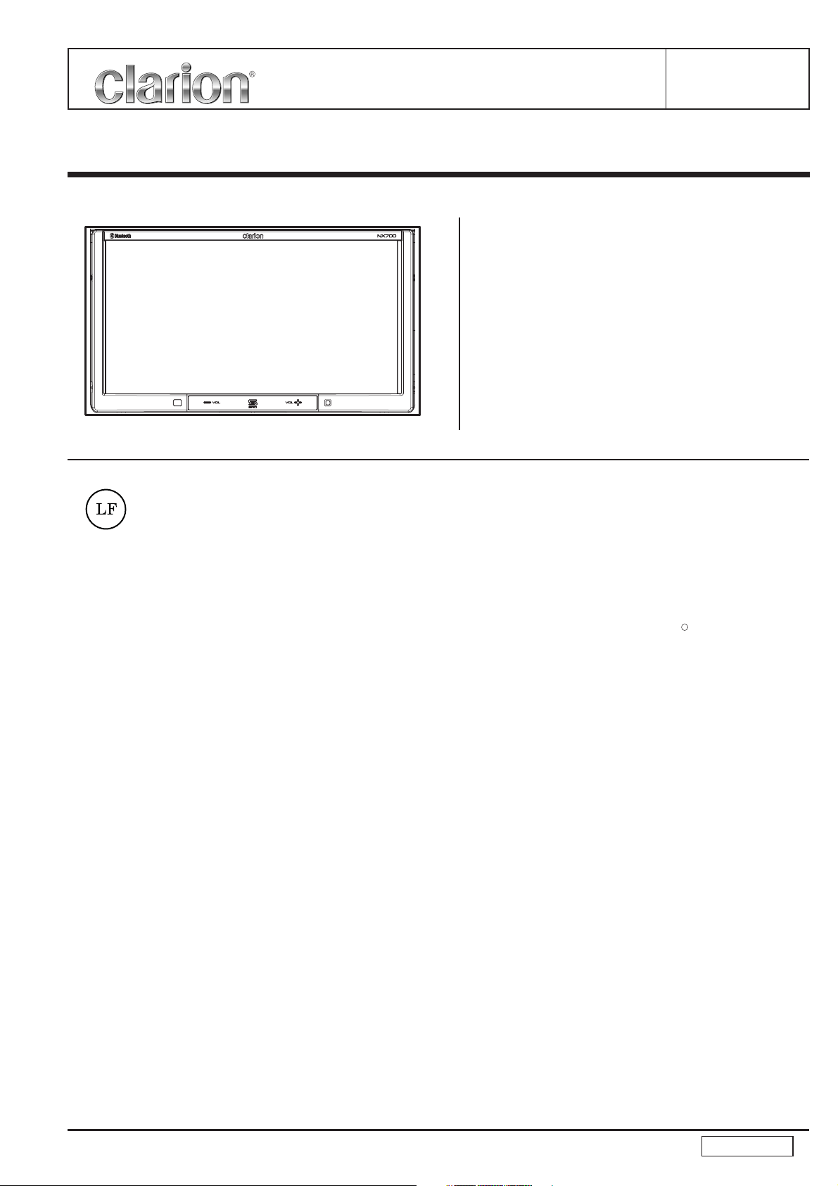
Service Manual
2-DIN Memory Navigation & DVD
Multimedia Station With 7-inch
Touch Panel Control
Published by Service Dept.
298-6753-00
Printed in Japan
Jan.2010
( NX700)
This product is a lead free model.
Lead free solder is used in PWB stamped LF mark.
Please keep the following conditions when you repair.
1. Use lead free solder.
* Koki's lead free solder S3X-55M 0.6mm
(CLARION Parts No.642-0231-01)
* Koki's lead free solder S3X-55M 1.0mm
(CLARION Parts No.642-0231-02)
2. Use a nitrogen solder system.
3. Do not use "General solder" and "Lead free solder"
together.
NOTES
* The internal parts of NAVI PWB ASSY cannot be repaired.
* When EEP-ROM IC(IC507:Main PWB) or TUNER
IC(IC101:Main PWB) is exchanged, it is necessary to
record the PRN file of A-Tomic tuner. Please refer to "ADJUSTMENTS".
* When LCD controller IC(IC103:Panel PWB) or Flash ROM
IC(IC104:Panel PWB) is exchanged, it is necessary to
setup the display. Please refer to "ADJUSTMENTS".
* It is necessary to record the program to microcomputer
(IC503:Main PWB) of a spare parts.
* When you exchange the parts in DVD mechanism(929-
2170-80), it is necessary to do inspection and adjustment
by special equipment.
Do not exchange the parts in DVD mechanism if there is
no special device.
* Specifications and design are subject to change without
notice for further improvement.
About the Registered Marks, etc.
* This product incorporates copyright protection technology
that is protected by U.S. patents and other intellectual prop-
Model
NX700
(QY-5014B-A)
(For North America : Region-1)
Model
NX700E
(QY-5015E-A)
(For Europe : Region-2)
erty rights. Use of this copyright protection technology must
be authorized by Macrovision, and is intended for home
and other limited viewing uses only unless otherwise authorized by Macrovision. Reverse engineering or disassembly is prohibited.
* Manufactured under license from Dolby Laboratories.
"Dolby" and the double-D symbol are trademarks of Dolby
Laboratories.
* Windows Media , and the Windows logo are trademarks,
or registered trademarks of Microsoft Corporation in the
United States and/or other countries.
* This product includes technology owned by Microsoft Cor-
poration and cannot be used or distributed without a license from MSLGP.
* "DivX", "DivX Certified", and associated logos are trade-
marks of DivX, Inc., and are used under license.
* "Made for iPod" means that an electronic accessory has
been designed to connect specifically to iPod and has been
certified by the developer to meet Apple performance standards.
"Works with iPhone" means that an electronic accessory
has been designed to connect specifically to iPhone and
has been certified by the developer to meet Apple performance standards.
Apple is not responsible for the operation of this device or
its compliance with safety and regulatory standards. iPod
is a trademark of Apple Inc., registered in the U.S. and
other countries.iPhone is a trademark of Apple Inc.
* BBE MP (Minimized Polynomial Non-Linear Saturation)
Process improves digitally compressed sound, such as
MP3, by restoring and enhancing the harmonics lost
through compression. BBE MP works by regenerating harmonics from the source material, effectively recovering
warmth, details and nuance.
* Manufactured under license from BBE Sound, Inc.
* Licensed by BBE Sound, Inc. under one or more of the
following US patents: 5510752, 5736897. BBE and BBE
symbol are registered trademarks of BBE Sound, Inc.
TM
R
- 1 -
NX700/NX700E
Page 2
SPECIFICATIONS
Tuner section : NX700(QY-5014B-A)
Frequency range: AM 530kHz to 1710kHz
FM 87.9MHz to 107.9MHz
Quieting sensitivity: AM Less than 37dBuV(S/N=20dB)
FM Less than 15dBuV(S/N=30dB)
Stereo separation: FM More than 25dB(ANT 65dBuV)
Auto stop sensitivity: AM DX 30+/-8dBuV
FM DX 25+/-8dBuV
S/N: AM More than 45dB
(ANT 74dBuV,0dB=1.41V)
FM More than 50dB
(ANT 55dBuV,0dB=1.41V)
Tuner section : NX700E(QY-5015E-A)
Frequency range: LW 153kHz to 279kHz
MW 531kHz to 1602kHz
FM 87.5MHz to 108.0MHz
Quieting sensitivity: LW Less than 45dBuV(S/N=20dB)
MW Less than 37dBuV(S/N=20dB)
FM Less than 15dBuV(S/N=30dB)
Stereo separation: FM More than 25dB(ANT 65dBuV)
Auto stop sensitivity: LW DX 30+/-8dBuV
LO 50+/-8dBuV
MW DX 30+/-8dBuV
LO 50+/-8dBuV
FM DX 22+/-8dBuV
LO 45+/-8dBuV
S/N: LW More than 45dB
(ANT 74dBuV,0dB=1.41V)
MW More than 45dB
(ANT 74dBuV,0dB=1.41V)
FM More than 50dB
(ANT 55dBuV,0dB=1.41V)
USB/AUX/2-ZONE section
Distortion: Less than 0.07%(1kHz,20kHz LPF)
S/N: More than 70dB
(1kHz,20kHz LPF JIS-A)
Stereo separation: More than 55dB(1kHz,20kHz LPF)
2-Zone line out: More than 200mV(1kHz)
* USB;MP3/128kbps
* AUX;Sens. HIGH,Input 0.65V
* 2-Zone;Disc TCD-782
LCD monitor section
Screen size: 7-inch wide type
152(W)x85(H)mm
Display method: Transmission type TN liquid
crystal display
Drive method: TFT(thin-film transistor)
active matrix driving
Pixels: 336,960(1440 RGB x 234)
General
Maximum power output:More than 27W x 4(CD,1kHz,Vol
Max,14.4V) [50W x 4 type]
Speaker impedance: 4 ohm(4 to 8 ohm)
Power source voltage: 14.4V DC
(10.8 to 15.6V allowable)
Ground: Negative
Current consumption: 3.5A(1W)
Auto antenna rated current:
500mA less
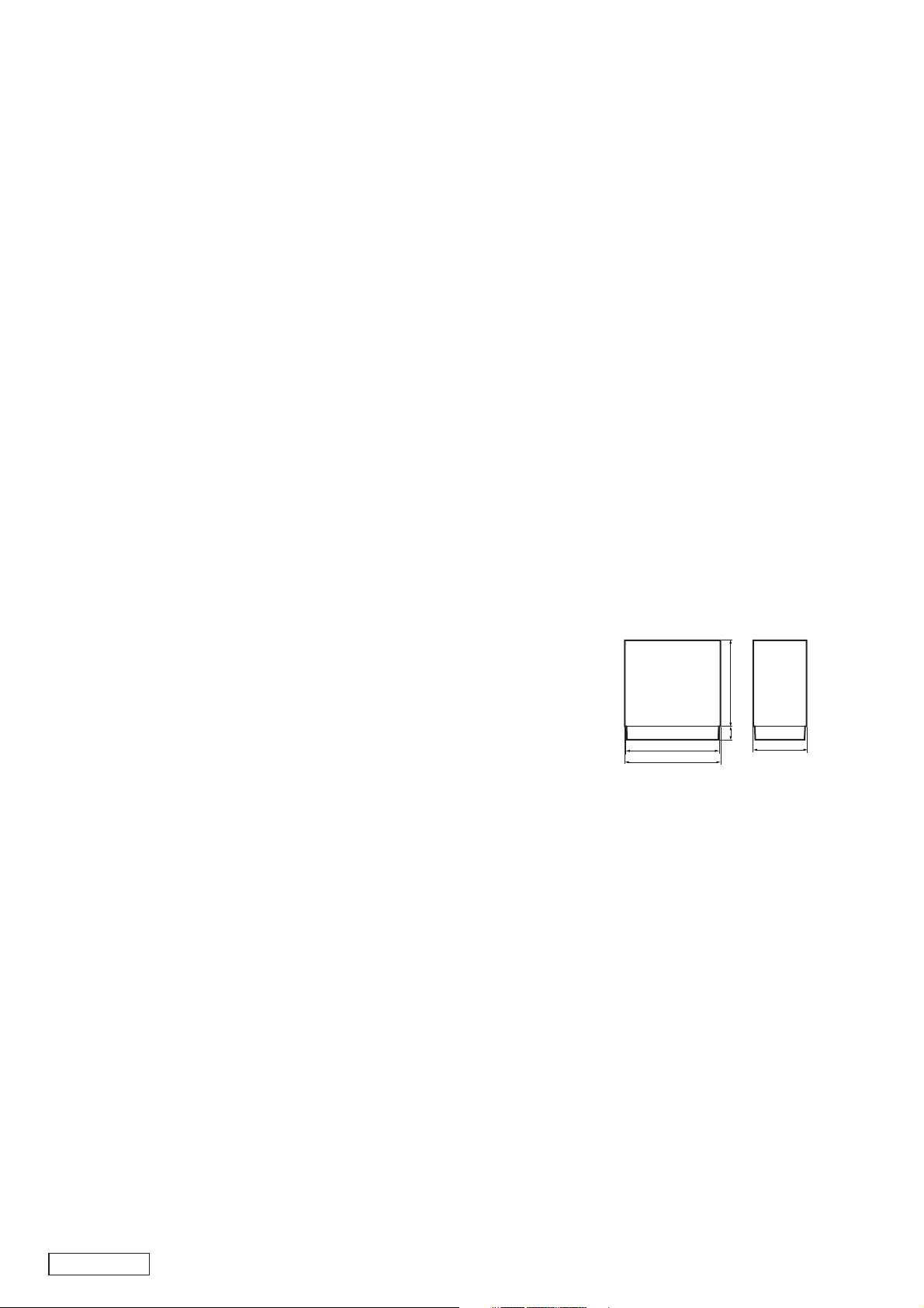
Dimensions(mm): Main unit
160mm
CD player section
Distortion: Less than 0.05%(1kHz,20kHz LPF)
S/N: More than 80dB
(1kHz,20kHz LPF JIS-A)
Stereo separation: More than 70dB(1kHz,20kHz LPF)
DVD player section
[DVD-VDEO LPCM48k L/R (DISC TDV-540)]
Line out: More than 1250mV
(1kHz 0dB,Vol Max)
Distortion: Less than 0.05%
(1kHz 0dB,20kHz LPF)
S/N: More than 80dB
(1kHz 0dB,20kHz LPF,JIS-A)
Separation: More than 70dB(20kHz LPF)
[Video output(NTSC) DISC TDV-540] : QY-5014B-A
Video output level: 1.0+/-0.2Vp-p
(75% SMPTE color bar NTSC)
White 100% level: 714+/-150mV
(75% SMPTE color bar NTSC)
Video S/N: More than 45dB(White 50% NTSC)
[Video output(PAL) DISC TDV-540] : QY-5015E-A
Video output level: 1.0+/-0.2Vp-p
(75% SMPTE color bar NTSC)
White 100% level: 700+/-150mV
(75% SMPTE color bar NTSC)
Video S/N: More than 45dB(White 50% NTSC)
171 mm
178 mm
Remote control unit
43.4(W)x12.5(H)x112.7(D)
Weight: Main unit Approx. 2.6kg
Remote control unit 60g
(including battery)
21.8mm
100 mm
NX700/NX700E
- 2 -
Page 3
To engineers in charge of repair or inspection of our products.
Before repair or inspection, make sure to follow the
instructions so that customers and Engineers in charge
of repair or inspection can avoid suffering any risk or injury.
1. Use specified parts.
The system uses parts with special safety features against fire
and voltage. Use only parts with equivalent characteristics when
replacing them.
The use of unspecified parts shall be regarded as remodeling for
which we shall not be liable. The onus of product liability (PL)
shall not be our responsibility in cases where an accident or failure is as a result of unspecified parts being used.
2. Place the parts and wiring back in their original positions after
replacement or re-wiring.
For proper circuit construction, use of insulation tubes, bonding,
gaps to PWB, etc, is involved. The wiring connection and routing
to the PWB are specially planned using clamps to keep away
from heated and high voltage parts. Ensure that they are placed
back in their original positions after repair or inspection.
If extended damage is caused due to negligence during repair,
the legal responsibility shall be with the repairing company.
3. Check for safety after repair.
Check that the screws, parts and wires are put back securely in
their original position after repair. Ensure for safety reasons there
is no possibility of secondary ploblems around the repaired spots.
If extended damage is caused due to negligence of repair, the
legal responsibility shall be with the repairing company.
4. Caution in removal and making wiring connection to the parts for
the automobile.
Disconnect the battery terminal after turning the ignition key off.
If wrong wiring connections are made with the battery connected,
a short circuit and/or fire may occur. If extensive damage is caused
due to negligence of repair, the legal responsibility shall be with
the repairing company.
5. Cautions in soldering
Please do not spread liquid flux in soldering.
Please do not wash the soldering point after soldering.
6. Cautions in soldering for chip capacitors
Please solder the chip capacitors after pre-heating for replacement because they are very weak to heat.
Please do not heat the chip capacitors with a soldering iron directly.
7. Cautions in handling for chip parts.
Do not reuse removed chips even when no abnormality is observed in their appearance. Always replace them with new ones.
(The chip parts include resistors, capacitors, diodes, transistors,
etc).
Please make an operation test after replacement.
8. Cautions in handling flexible PWB
Before working with a soldering iron, make sure that the iron tip
temperature is around 270
repeatedly(more than three times)to the same patterns. Also take
care not to apply the tip with force.
9. Turn the unit OFF during disassembly and parts replacement.
Recheck all work before you apply power to the unit.
10. Cautions in checking that the optical pickup lights up.
The laser is focused on the disc reflection surface through the
lens of the optical pickup. When checking that the laser optical
. Take care not to apply the iron tip
diode lights up, keep your eyes more than 30cms away from the
lens. Prolonged viewing of the laser within 30cms may damage
your eyesight.
11. Cautions in handling the optical pickup
The laser diode of the optical pickup can be damaged by electrostatic charge caused by your clothes and body. Make sure to
avoid electrostatic charges on your clothes or body, or discharge
static electricity before handling the optical pickup.
11-1. Laser diode
The laser diode terminals are shorted for transportation in order
to prevent electrostatic damage. After replacement, open the
shorted circuit. When removing the pickup from the mechanism,
short the terminals by soldering them to prevent this damage.
11-2. Actuator
The actuator has a powerful magnetic circuit. If a magnetic material is put close to it. Its characteristics will change. Ensure that
no foreign substances enter through the ventilation slots in the
cover.
11-3. Cleaning the lens
Dust on the optical lens affects performance.
To clean the lens, apply a small amount of isopropyl alcohol to
lens paper and wipe the lens gently.
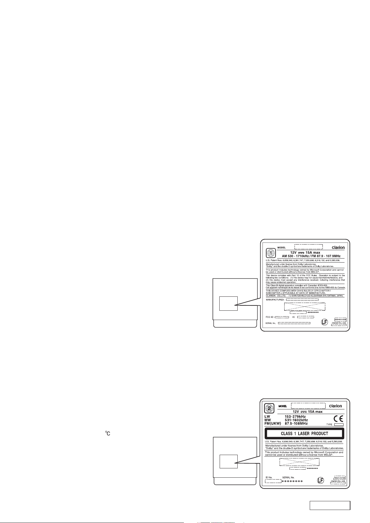
CAUTION
NX700(QY-5014B-A) : for North America
Change or modifications to this product not approved by the
manufacture will void the warranty and will violate FCC approval.
Top view of QY-5014B-A
NX700E(QY-5015E-A) : for Europe
This appilance contains a laser system and is classified as a
"CLASS 1 LASER PRODUCT" . In case of any trouble with
this player, please contact your nearest "authorized service
station" . To prevent direct exposure to the laser beam, do not
try to open the enclosure.
Top view of QY-5015E-A
Setplate
Setplate
- 3 -
NX700/NX700E
Page 4
COMPONENTS
QY-5014B-A
1. Main unit ----------- 1
2. Remote control unit RCB-198-600 1
(Battery CR2025 ----------- 1)
3. Microphone 081-0039-01 1
4. GPS antenna 096-0151-00 1
5. Finisher 383-0752-00 1
6. Power supply cord 854-6488-50 1
(15A FUSE 120-0150-00 1)
(3A FUSE 120-0030-00 1)
7. RCA pin cord 855-5576-50 1
8. Bag for accessories ----------- 1
8-1. Lead holder 321-1026-01 3
8-2. Rubber cap(for RCA pin cord) 345-3799-20 14
8-3. Double-sided tape(for fastening GPS antenna)
347-6369-20 1
8-4. Flat head screw(M5x8) 714-5008-4B 8
8-5. Hexagonal screw(M5x8) 716-0496-51 8
1
Main unit
4
GPS antenna
7
RCA pin cord
QY-5015E-A
1. Main unit ----------- 1
2. Microphone 081-0039-01 1
3. GPS antenna 096-0151-00 1
4. Power supply cord 854-6495-50 1
(15A FUSE 120-0150-00 1)
5. RCA pin cord 855-5576-50 1
6. Bag for accessories ----------- 1
6-1. Electro tap 060-0018-00 1
6-2. Lead holder 321-1026-01 3
6-3. Rubber cap(for RCA pin cord) 345-3799-20 14
6-4. Double-sided tape(for fastening GPS antenna)
347-6369-20 1
6-5. Flat head screrw(M5x8) 714-5008-4B 8
6-6. Hexagonal screw(M5x8) 716-0496-51 8
1 4
Main unit
Microphone RCA pin cord
2 5
Power supply cord
15A FUSE
6
Bag for accessories
6-1 6-2
6-3 6-4
Remote control unit
2 5
(Battery)
3
Microphone
Finisher
6
Power supply cord
15A / 3A FUSE
Bag for accessories
8
8-1
8-3
8-5
8-2
8-4
3
GPS antenna
6-5
6-6
NX700/NX700E
- 4 -
Page 5
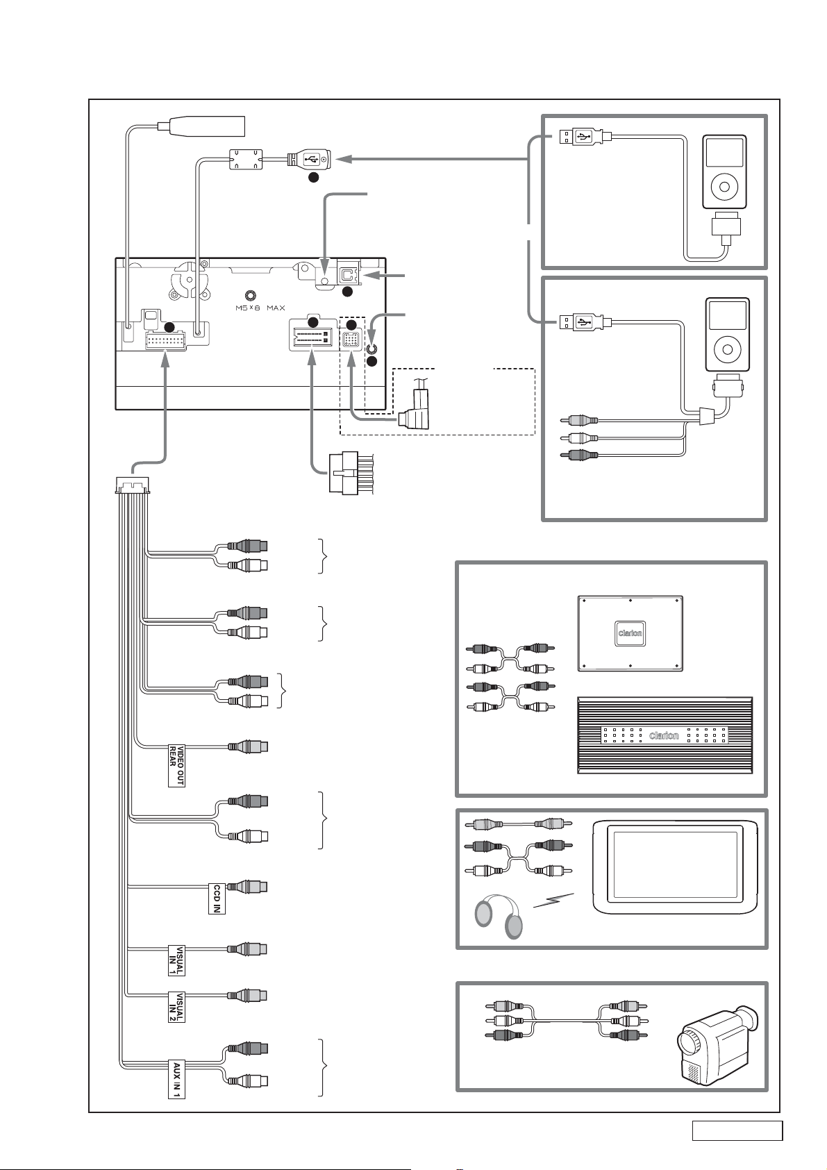
CONNECTIONS
Wire connections
2
RCA pin cord
(855-5576-50)
Red
Gray
White
Red
Black
White
Red
Purple
White
Gray
Yellow
Radio antenna jack
USB terminal
Right
Left
Right
Left
Subwoofer output
terminal (MONO 2ch)
Video output terminal
6
5
1
3
Front audio
output terminal
Rear audio
output terminal
Microphone terminal of
Bluetooth phone
(Connects the supplied
microphone.)
GPS antenna jack
Steering wheel
remote control
terminal
4
< NX700 >
CeNET terminal
Power supply cord
(NX700 : 854-6488-50)
(NX700E : 854-6495-50)
iPod/iPhone
Connector cable
or
iPod with video/iPhone
Connector cable
(CCA-723/CCA-748)
Connect to the AUX audio
input terminal and the iPod video
input terminal.
4-Channel Amplifier
(NX700)
Green
Black
Black
Black
Red
Red
White
Yellow
Yellow
Yellow
Red
White
Right
Left
(2-Zone audio
output terminal)
Rear Vision Camera
terminal
AUX video input terminal
iPod video input terminal
Right
AUX audio
Left
input terminal
- 5 -
(NX700E)
Rear Monitor
Wireless Head phone
VTR etc.
Connect to the AUX audio/
video input terminal.
NX700/NX700E
Page 6
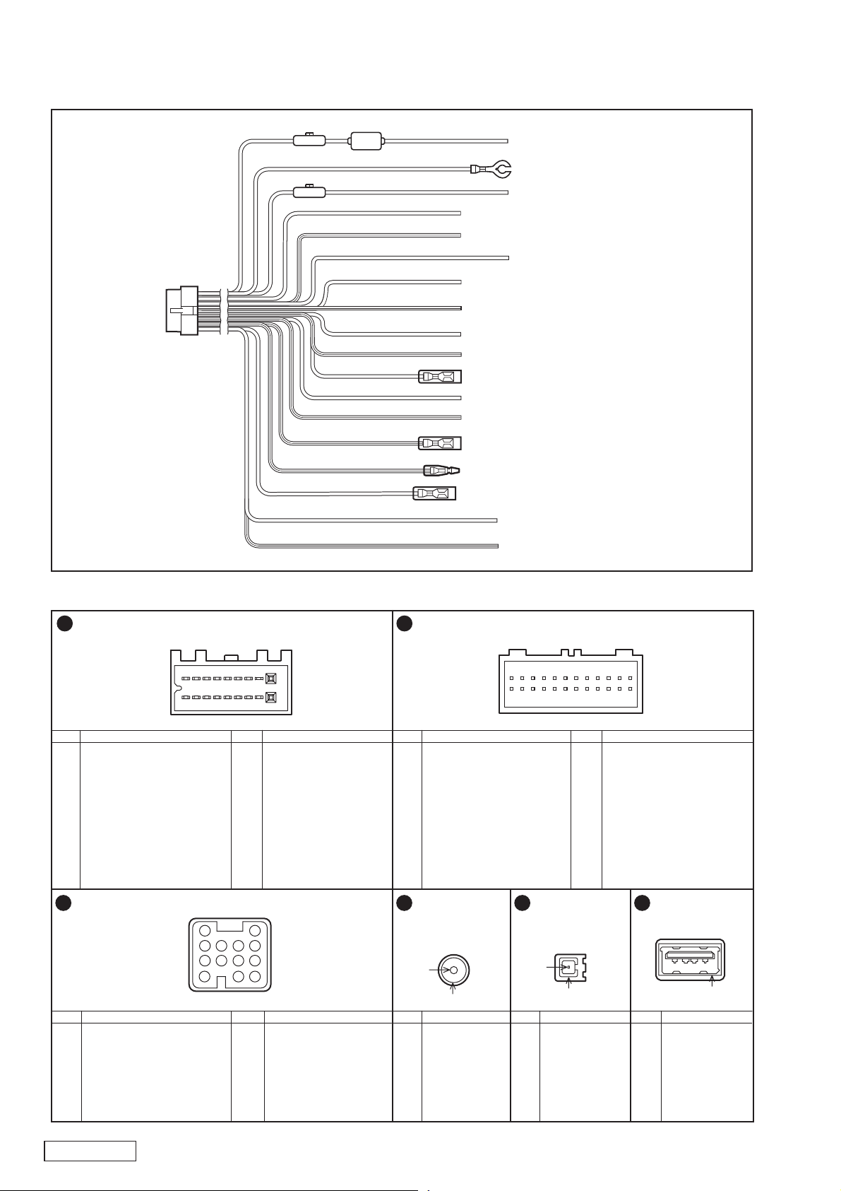
< NX700 (QY-5014B-A) >
Power supply cord (854-6488-50)
15A
3A
Yellow
Black
Yellow
Purple
Purple/Black
Red
Gray
Gray/Black
White
White/Black
Brown
Green
Green/Black
Blue/White
Orange/White
Blue
Grass-green
Purple/white
+12V main power(BACK UP)
Ground(GND)
CeNET bus backup
Rear right (+)
Rear right (-)
+12V accessory(ACC)
Front right (+)
Front right (-)
Front left (+)
Front left (-)
No connection
Rear left (+)
Rear left (-)
Amplifier turn-on cord(AMP REMOTE)
Illumination
Auto antenna
Parking brake cord
Reverse gear cord
Connectors
1
Power supply connector
Main PWB J601
Pin name
No.
REAR L-CH (-)
1
REVERSE GEAR
2
REAR L-CH (+)
3
PARKING BRAKE
4
FRONT L-CH (-)
5
N.C.
6
FRONT L-CH (+)
7
ACC
8
FRONT R-CH (+)
9
AUTO ANTENNA
10
FRONT R-CH (-)
11
AMP REMOTE
12
3
CeNET terminal
Main PWB J602
Pin name
No.
GND
1
B/U +14V
2
BUS AUDIO L-CH (+)
3
N.C.
4
N.C.
5
BUS (+)
6
BUS AUDIO R-CH (+)
7
BUS AUDIO R-CH (-)
8
123456789101113
for Sirius/XM
1
12
13
17
141516
18
Pin name
No.
REAR R-CH (+)
13
ILLUMINATION
14
REAR R-CH (-)
15
BUS BACK UP
16
BACK UP
17
GND
18
1211
10987
6543
2
Pin name
No.
SYSTEM ACC
9
BUS (-)
10
BUS AUDIO L-CH (-)
11
N.C.
12
N.C.
13
2
RCA connector
Main PWB P203
Pin name
No.
LINE OUT REAR L-CH
1
LINE OUT REAR R-CH
2
LINE OUT FRONT L-CH
3
LINE OUT FRONT R-CH
4
S-GND
5
S-GND
6
SUB-WOOFER L-CH
7
SUB-WOOFER R-CH
8
S-GND
9
S-GND
10
2-ZONE L-CH
11
2-ZONE R-CH
12
4
Steering wheel
remote control
terminal
Main PWB J506
1
2
Pin name
No.
REMOTE CONT
1
SHIELD GND
2
1234567891011 13
12 14151617181920
5
GPS antenna
jack
Navi PWB assy
1
2
Pin name
No.
RF IN
1
GPS GND
2
212223
24
Pin name
No.
REAR VIDEO OUTPUT GND
13
VIDEO INPUT-1 GND
14
REAR VIDEO OUTPUT
15
VIDEO INPUT-1
16
AUX INPUT-1 L-CH GND
17
AUX INPUT-1 R-CH GND
18
AUX INPUT-1 L-CH
19
AUX INPUT-1 R-CH
20
VIDEO INPUT-2 GND
21
CCD CAMERA GND
22
VIDEO INPUT-2
23
CCD CAMERA INPUT
24
6
USB terminal
Main PWB
Pin name
No.
VBUS
1
USB D (-)
2
USB D (+)
3
GND
4
SHIELD GND
5
3
2
1
4
5
NX700/NX700E
- 6 -
Page 7
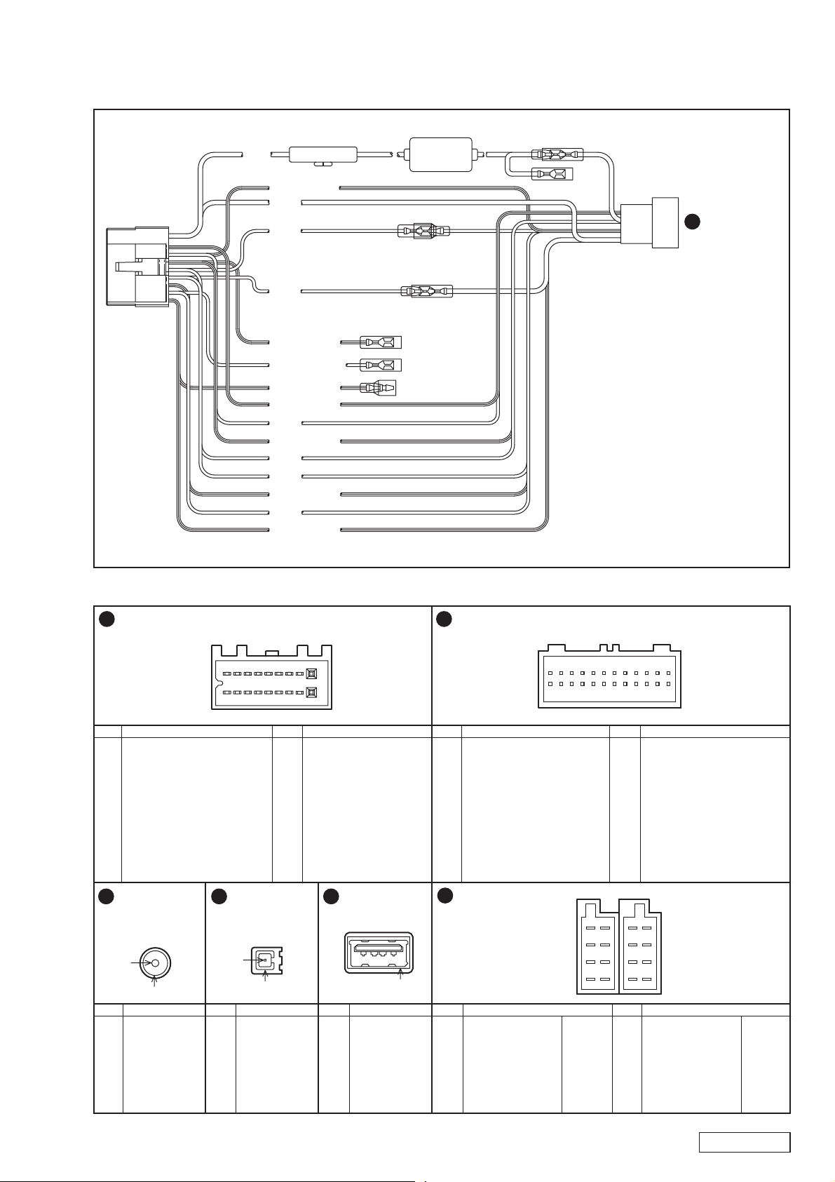
< NX700E (QY-5015E-A) >
Power supply cord (854-6495-50)
YEL
FUSE(15A)
ORG / WHT
BLK
BLU
RED
BLU / WHT
GRASS GRN
PUR / WHT
PUR / BLK
PUR
GRY / BLK
GRY
WHT
WHT / BLK
GRN
GRN / BLK
BACK UP
1
*
(Spare)
7
ACC
1
*
Note:
1 In certain vehicles -
*
2
*
AMP REMOTE
PARKING BRAKE
REVERSE GEAR
Volkswagen/Opel/Vauxhall - it is
necessary to exchange the accessory
<<Red>> and the main power
<<Yellow>> connection, to avoid
overload and loss of memory.
2 When the unit is installed in a 1998 or
*
later Volkswagen model, make sure to
interrupt the <<Remote>> output.
Disconnect the <<blue/white>> wire
and insulate the front ends of this cord.
A breakdown may occur if the cord is
not disconnected, or front ends are not
insulated.
Connectors
1
Power supply connector
Main PWB J601
Pin name
No.
REAR L-CH (-)
1
REVERSE GEAR
2
REAR L-CH (+)
3
PARKING BRAKE
4
FRONT L-CH (-)
5
N.C.
6
FRONT L-CH (+)
7
ACC
8
FRONT R-CH (+)
9
AUTO ANTENNA
10
FRONT R-CH (-)
11
AMP REMOTE
12
4
Steering wheel
remote control
terminal
Main PWB J506
1
2
Pin name
No.
REMOTE CONT
1
SHIELD GND
2
123456789101113
5
GPS antenna
jack
Navi PWB assy
1
2
Pin name
No.
RF IN
1
GPS GND
2
12
17
141516
18
Pin name
No.
REAR R-CH (+)
13
ILLUMINATION
14
REAR R-CH (-)
15
N.C.(BUS BACK UP)
16
BACK UP
17
GND
18
6
USB terminal
Main PWB
1
Pin name
No.
VBUS
1
USB D (-)
2
USB D (+)
3
GND
4
SHIELD GND
5
2
RCA connector
Main PWB P203
1234567891011 13
12 14151617181920
Pin name
No.
LINE OUT REAR L-CH
1
LINE OUT REAR R-CH
2
LINE OUT FRONT L-CH
3
LINE OUT FRONT R-CH
4
S-GND
5
S-GND
6
SUB-WOOFER L-CH
7
SUB-WOOFER R-CH
8
S-GND
9
S-GND
10
2-ZONE L-CH
11
2-ZONE R-CH
12
7
ISO connector
Power supply cord
3
2
4
5
Pin name
No.
N.C.
A-1
N.C.
A-2
N.C.
A-3
BACK UP
A-4
A-5
AUTO ANTENNA
A-6
ILLUMINATION
A-7
ACC
A-8
GND
(BATTERY)
(ACCESSORY
(GROUND)
A
2
1
3
4
5
6
7
8
-
-
-
YEL
BLU
ORG/WHT
)
RED
BLK
212223
24
Pin name
No.
REAR VIDEO OUTPUT GND
13
VIDEO INPUT-1 GND
14
REAR VIDEO OUTPUT
15
VIDEO INPUT-1
16
AUX INPUT-1 L-CH GND
17
AUX INPUT-1 R-CH GND
18
AUX INPUT-1 L-CH
19
AUX INPUT-1 R-CH
20
VIDEO INPUT-2 GND
21
CCD CAMERA GND
22
VIDEO INPUT-2
23
CCD CAMERA INPUT
24
B
2
1
3
4
5
6
7
8
Pin name
No.
REAR R-CH (+)
B-1
REAR R-CH (-)
B-2
FRONT R-CH (+)
B-3
FRONT R-CH (-)
B-4
FRONT L-CH (+)
B-5
FRONT L-CH (-)
B-6
REAR L-CH (+)
B-7
REAR L-CH (-)
B-8
PUR
PUR/BLK
GRY
GRY/BLK
WHT
WHT/BLK
GRN
GRN/BLK
- 7 -
NX700/NX700E
Page 8
TROUBLE SHOOTING
General
NO POWER AUDIO OUTPUT TROUBLE (RADIO MODE)
CHECK ITEM CHECK POINT CHECK ITEM CHECK POINT
1 POWER SUPPLY WIRE CONNECTIONS
FUSE
CONNECTORS 2 AROUND IC101(TUNER IC)
BATTERY
2 4V POWER SUPPLY 4V STB
Q634,IC602
3 OSCILLATION OF X501 X501 1 I2S CONNECTION OF DVD MECHANISM
4 RESET IC IC506 FPC, J401
5 B/U-6V-DET IC504,R580,R587
6 B/U-9V-DET2 IC505,Q501
7 ACC-DET IC505,Q502,Q503
8 SYSTEM CONTROLLER(IC503)
KEY OPERATION TROUBLE
CHECK ITEM CHECK POINT 2 INPUT OF IC209(E-VOL) AROUND IC205(AUX1 GAIN)
1 KEY CONDITION KEYS
2 SWITCH CONDITION SWITCHES
3 INPUT OF IC503 J901(PANEL-B),FPC,J105(PANEL-A)
4 SYSTEM CONTROLLER(IC503)
RADIO TROUBLE
CHECK ITEM CHECK POINT
1 ANTENNA CONNECTION OF ANTENNA
2 SEEK AROUND IC101(TUNER IC)
3 AV8.5V POWER SUPPLY Q620,Q621
4 OUTPUT OF SIGNAL PINS 8 AND 9 OF IC101
(AUDIO SIGNAL)
5 AUDIO LINE
Audio
AUDIO OUTPUT TROUBLE (SPEAKER AND LINE OUT)
CHECK ITEM CHECK POINT
1 OFFSET DET CONNECTION OF SPEAKERS
INPUT DC OF IC601(POWER IC)
2 AV8.5V POWER SUPPLY Q620,Q621
3 E-VOL IC209(E-VOL), IC503
4 AUDIO-GND AUDIO-GND LINE
5 OUTPUT OF E-VOL PINS 12,13,14,19,20 AND 21 OF
IC209(AUDIO LINE)
6 MUTE Q203,Q204,Q205,Q206,Q207,
Q208,Q209,Q210
7 SYSTEM CONTROLLER(IC503)
1 AUDIO OF TUNER IC PINS 8 AND 9 OF IC101(TUNER IC)
AUDIO OUTPUT TROUBLE (CD/DVD MODE)
CHECK ITEM CHECK POINT
2 AROUND IC200(DAC)
AUDIO OUTPUT TROUBLE (AUX1)
CHECK ITEM CHECK POINT
1 RCA CONNECTION OF RCA
3 AROUND IC209(E-VOL)
AUDIO OUTPUT TROUBLE (NAVI GUIDE)
CHECK ITEM CHECK POINT
1 CONNECTION CONNECTIONS
2 INPUT OF IC209(E-VOL) AROUND IC207(NAVI+/-)
3 AROUND IC209(E-VOL)
C220,C221
CONNECTORS
CONNECTORS
FRONT SPEAKER
Radio
RADIO DOES NOT WORK
CHECK ITEM CHECK POINT
1 AUDIO8.5V L108,L109(VCC LINE)
2 LINE OF TUNER R106,R107,
3 TUNER IC(IC101)
RECEIVE/SEEK TROUBLE
CHECK ITEM CHECK POINT
1 ANTENNA
2 GUARD OF ANT AMP-REM,A-ANT LINE
3 AUDIO8.5V L108,L109(VCC LINE)
READING OF PARAMETER
4
5 PARAMETER READJUST
6 TUNER IC(IC101)
L222,L223
CONNECTION OF ANTENNA
CURRENT CONSUMPTION
IC503(SYSTEM),IC507(E2PROM)
AUDIO OUTPUT TROUBLE (SPEAKER)
CHECK ITEM CHECK POINT
1 SPEAKER CONNECTION OF SPEAKERS
2 AMP-STB,AMP-MUTE IC601(POWER IC)
3 INPUT SIGNAL IC601(POWER IC)
4 AUDIO LINE(C324,C325,C326,C327)
AUDIO OUTPUT TROUBLE (LINE OUT)
CHECK ITEM CHECK POINT
1 AMP-REM CONNECTION OF AMP-REM
2 GUARD OF REM AMP-REM,A-ANT LINE
CURRENT CONSUMPTION
3 RCA CONNECTION OF RCA
4 AUDIO-GND GND OF EXTERNAL AMP
5 EXTERNAL AMP
NX700/NX700E
- 8 -
Page 9
Slide Mechanism
SLIDE-MECH TROUBLE
CHECK ITEM CHECK POINT
1 POSITION OF SD CARD SETTING OF SD CARD
2 VOLTAGE OF TP353
AND TP355
3 MOTOR 8V IC751, IC503
4 MOTOR DRIVER IC508, J502, J5001, P5603
5 SLIDE MECHANISM
J382, NAVI PWB
Navigation
NAVIGATION TROUBLE
CHECK ITEM CHECK POINT
1 POWER SUPPLY OF
NAVI PWB
2 SYS-ACC(TP366)=LO Q383, IC503, J382
3 RESET(TP368)=LO Q384, IC503, J382
4 N-MONI(TP367)=LO Q385, IC503, J382
5 TX, RX LINE IC503, J382
6 NAVI PWB ASSY
J382
CONNECTION OF NAVI PWB
Panel
DISPLAY TROUBLE(BLACK DISPLAY)
CHECK ITEM CHECK POINT
1 INPUT OF INVERTER CONNECTION OF J452:MAIN PWB
J103, P701,F701(FUSE)
2 INPUT OF IC103 VIDEO:C128
NAVI:C137,C129,C130,C131
3 LEAK SHIELD CASE(INVERTER)
ARAMID
POWER SUPPLY VOLTAGE
4
OUTPUT OF INVERTER(IC702)
5
T701
DISPLAY TROUBLE(WHITE DISPLAY)
CHECK ITEM CHECK POINT
1 INPUT SIGNAL OF PANEL
POWER SUPPLY VOLTAGE
2
3 OSCILLATION OF IC103 X101
4 DET ,RESET OF IC103 PIN 71 OF IC103(RESET)
5 TOUCH PANEL AROUND IC103(TP CONTROL)
6 FLASH ROM AROUND IC104(FLASH)
7 DC/DC OF IC103 Q103(1.8V),Q107(3.3V),Q100(18.5V)
8 OUTPUT LCD CONTROLLER(IC103)
DISPLAY TROUBLE(SYNCHRONIZATION)
CHECK ITEM CHECK POINT
1 INPUT SIGNAL OF PANEL
POWER SUPPLY VOLTAGE
2
3 TOUCH PANEL (REFER TO T/P SECTION)
4 INPUT OF IC103 VIDEO:PIN 29 OF J103
5 AROUND LCD CONTROLLER(IC103)
IC702(INVERTER), D701
J452:MAIN PWB
J103
IC103(CONTROLLER),IC104(FLASH)
J452:MAIN PWB
J103
IC103(LCD CONTROLLER)
NAVI:C137,C129,C130,C131
DISPLAY TROUBLE(NOT LIGHT THE BACKLIGHT)
CHECK ITEM CHECK POINT
1 POSITION OF
BACKLIGHT LEAD
2 CONNECTION OF
CONNECTOR
3 FL+B(TP712) F701, FL+B LINE(MAIN PWB)
4 ENA(TP770)
DIMMER(TP708)
5 SHORT OF MOSES
(32, 38PIN OF IC103)
AND GND
CIRCUIT LINE OF INVERTER
6
DISPLAY TROUBLE(LIGHT THE BACKLIGHT)
CHECK ITEM CHECK POINT
1 CONTACT OF CONTACT OF
PANEL PWB AND
SHEET METAL OF
FULL AUTO MECH
CONNECTION OF
2 PANEL: J103
CONNECTOR
3
POWER SUPPLY
TO DISPLAY
4
RGB OUTPUT OF
DISPLAY
OPERATION OF PORT
5
6
POWER SUPPLY(3.3V) OF
F-ROM(IC104)
7
COMMUNICATION OF
PORT
8
AROUND CIRCUIT LINE OF MOSES(IC103)
PORT OF F-ROM(IC104) AND MICOM(IC503)
DISPLAY TROUBLE(WHITE DISPLAY,HORIZONTAL LINE,SCREEN BEAT)
CHECK ITEM CHECK POINT
1 RESET
WRITING OF F-ROM(IC104)
2
CONTACT OF
3
ELECTRICAL PARTS OF
PANEL PWB
AND BRACKET
POWER SUPPLY
4
TO DISPLAY
5 RGB OUTPUT OF
DISPLAY
6 TCON OUTPUT OF
DISPLAY
7 AROUND CIRCUIT LINE OF MOSES(IC103)
PORT OF F-ROM(IC104) AND MICOM(IC503)
CONTACT OF LEAD AND
SHEET METAL
CONNECTIONS
PANEL: J103,P701
MAIN: J452
ENA/DIMMER LINE
MOSES LINE
SPIKE NOISE IN MOSES PORT
PANEL PWB TP AND
SHEET METAL
MAIN: J452
3.3V(TP162), VGL(TP177),
VGH(TP173), 5V(TP171)
RESISTOR OF RGB LINE
5V SUPPLY TO
MOSES(130PIN OF IC103)
MOSES(126, 127PIN OF IC103)
MOS_BUF_DET(TP111): H
MOS_RST_DET(TP112): H
MOS_RESET(TP115): L
POWER SUPPLY(3.3V) FILTER OF
F-ROM(IC104)
* MOSES(IC103)
68PIN: CS; H
69PIN: SCL, 70PIN: SDA
74PIN: SPI_SDO; OPERATION
* F-ROM(IC104)
16PIN: SPI_SCK, 15PIN(SPI_SDI)
7PIN: CS; OPERATION
9PIN: W; L
SOFTWARE
NORMAL WRITING OF F-ROM(IC104)
SHORT OF
ELECTRICAL PARTS OF
PANEL PWB
AND BRACKET
3.3V(TP162), VGL(TP177),
VGH(TP173), 5V(TP171)
RESISTOR OF RGB LINE
5V SUPPLY TO
MOSES(130PIN OF IC103)
MOSES(126, 127PIN OF IC103)
RESISTOR OF TCON LINE
PORT OF MOSES(IC103)
- 9 -
NX700/NX700E
Page 10
DISPLAY TROUBLE(OSD)
CHECK ITEM
1 RESET
WRITING OF F-ROM(IC104)
2
SOFTWARE
NORMAL WRITING OF F-ROM(IC104)
CHECK POINT
3 CIRCUIT LINE OF F-ROM(IC104)
DISPLAY TROUBLE(DVD)
CHECK ITEM CHECK POINT
1 PKB TO GND CIRCUIT LINE OF PKB
2 CONNECTION OF
DVD MECH CONNECTOR
MAIN: CONNECTOR OF DVD MECH
AND FLEX PWB
3 OPERATION OF DVD DVD MECH
MAIN POWER SUPPLY LINE
4 CVBS SIGNAL LINE ELECTRICAL PARTS OF
(800mVp-p) OF CVBS SIGNAL LINE
MOSES(21PIN OF IC103)
INPUT OF
5
POWER SUPPLY TO
ELECTRICAL PARTS OF
ADC 3.3V LINE
MOSES
(5, 23PIN OF IC103)
6 RGB OUTPUT OF
DISPLAY
RESISTOR OF RGB LINE
5V SUPPLY TO
MOSES(130PIN OF IC103)
MOSES(126, 127PIN OF IC103)
7 AROUND CIRCUIT LINE OF MOSES(IC103)
PORT OF F-ROM(IC104) AND MICOM(IC503)
DISPLAY TROUBLE(NAVI)
CHECK ITEM CHECK POINT
1 CONNECTION TO
COMBINATION OF NAVI
NAVI PWB ASSY
RGB SIGNAL LINE
2
(650mVp-p) OF
MOSES(7,9,10PIN OF IC103)
SYNC SIGNAL LINE
3
(200mVp-p) OF
ELECTRICAL PARTS OF
RGB SIGNAL LINE
ELECTRICAL PARTS OF
SYNC SIGNAL LINE
MOSES(8PIN OF IC103)
4
INPUT OF
POWER SUPPLY TO
ELECTRICAL PARTS OF
ADC 3.3V LINE
MOSES
(5, 23PIN OF IC103)
5
RGB OUTPUT OF
DISPLAY
RESISTOR OF RGB LINE
5V SUPPLY TO
MOSES(130PIN OF IC103)
MOSES(126, 127PIN OF IC103)
6
AROUND CIRCUIT LINE OF MOSES(IC103)
PORT OF F-ROM(IC104) AND MICOM(IC503)
TOUCH PANEL TROUBLE (DISPLAY)
CHECK ITEM
1 INPUT SIGNAL OF PANEL
J452:MAIN PWB
CHECK POINT
J103
2 DISPLAY (REFER TO PANEL SECTION)
3 CONDITION OF T/P SWITCH, TOCH PANEL
4 CONTROL LINE LINE OF IC103 AND T/P
5 AROUND LCD CONTROLLER(IC103)
TOUCH PANEL TROUBLE (CONNECTION)
CHECK ITEM
1 CONNECTION OF
PANEL: J102
CHECK POINT
CONNECTOR
2 FORM OF TOUCH PANEL
(PUSH DOUBLE)
INSTALLATION OF TOUCH PANEL
AT MOUNT
3 OUTPUT WAVEFORM OF CONNECTION
TOUCH PANEL
Q106, Q107
AT PUSHING
4 ELECTRICAL PARTS OF
OUTPUT WAVEFORM OF
TOUCH PANEL
TOUCH PANEL LINE
AT PUSHING
5 STATIC ELECTRICITY OF A/D PORT
SHORT OF MOSES
(58,59,60,61PIN OF IC103)
(IC103)
AND GND
6
INPUT OF MICOM TO
MOSES
ELECTRICAL PARTS OF
MOSES LINE(79, 80PIN OF IC103)
(79, 80PIN OF IC103)
7 AROUND CIRCUIT LINE OF MOSES(IC103),
PORT OF F-ROM(IC104) AND MICOM(IC503)
VERSION UP TROUBLE FOR F-ROM
CHECK ITEM CHECK POINT
1 F-ROM(IC104)
WRITING SOFTWARE
2
3
9PIN OF F-ROM(IC104)
SETTING OF F-ROM
ORDER TO WRITING SOFTWARE
H: WRITING SOFTWARE
ELECTRICAL PARTS OF
9PIN WRITE PROTECT LINE OF
F-ROM(IC104)
4
COMMUNICATION OF
PORT
* MOSES(IC103)
68PIN: CS; H
69PIN: SCL, 70PIN: SDA
74PIN: SPI_SDO; OPERATION
* F-ROM(IC104)
16PIN: SPI_SCK, 15PIN(SPI_SDI)
7PIN: CS; OPERATION
9PIN: W; L
5 AROUND CIRCUIT LINE OF MOSES(IC103)
PORT OF F-ROM(IC104) AND MICOM(IC503)
USER ADJ TROUBLE(BRIGHT, COLOR, HUE, CONTRAST)
CHECK ITEM
1 RESET
2
VERSION OF MICOM, F-ROM
SOFTWARE
NORMAL WRITING OF SOFTWARE
CHECK POINT
3 SOFTWARE
USER ADJ TROUBLE(DIMMER)
CHECK ITEM CHECK POINT
1 RESET
VERSION OF MICOM, F-ROM
2
3
DIMMER(TP708)
4
SHORT OF MOSES
SOFTWARE
NORMAL WRITING OF SOFTWARE
DIMMER LINE, CIRCUIT LINE OF MOSES
SPIKE NOISE IN MOSES PORT
(32, 38PIN OF IC103)
AND GND
5 CIRCUIT LINE OF INVERTER
ONLY USER ADJ: SOFTWARE
NX700/NX700E
DISPLAY COLOR TROUBLE(RGB-GAIN BALANCE)
CHECK ITEM CHECK POINT
1 COLOR OF OSD DISPLAY
ELECTRICAL PARTS OF RGB LINE
(R178, R179, R180, C181, C182, C183)
PORT OF MOSES(IC103)
DISPLAY
COLOR OF NAVI DISPLAY NAVI AUTO SETTING ADJUSTMENT
2
CONTRAST, WHITE BALANCE(R, B)
NAVI PWB ASSY
ELECTRICAL PARTS OF
RGB INPUT LINE
TO 7PIN - 10PIN OF MOSES(IC103)
COLOR OF AUX DISPLAY
3
SETTING OF AUX INPUT
CIRCUIT LINE OF AUX(MAIN SIDE)
DVD MECH, AROUND CIRCUIT, MOSES(IC103)
4
- 10 -
Page 11
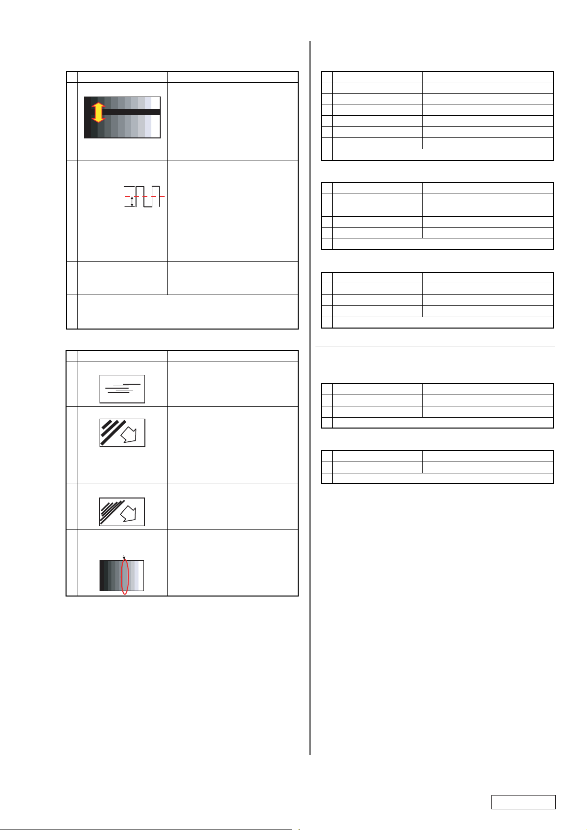
SCREEN FLICKER
CHECK ITEM
1 HORIZONTAL LINE
NECK AND THE LOUPE ARE
SHAKEN UP AND DOWN,
HORIZONTAL LINE IS FLICKER.
2 DC VOLTAGE OF TP172:
VCOM_DC ADJUSTMENT
VCOM_DC ADJUSTMENT, DISPLAY
APPROX. 1.0V TO 2.0V
THE CENTER VALUE
OF VOLTAGE
MEASURE THE CENTER VALUE
OF VOLTAGE OR
MEASURE THE DC VOLTAGE
WITH THE TESTER
ABOUT THE DC VOLTAGE
OF TP172.
3
VOLTAGE OF
OP9V(TP151), VGL(TP177)
CIRCUIT LINE OF VCOM, OP9V, VGL
AND VGH
PORT OF MOSES(IC103)
4
5V POWER VOLTAGE(MAIN_DD CON)
CONNECTION OF FLEX PWB
ELECTRICAL PARTS OF MOSES(IC103)
CHECK POINT
DVD/CD
LOADING/EJECT TROUBLE
CHECK ITEM CHECK POINT
1 DVD8V L412,Q403,FPC,J401,MECH
2 DVD3.3, 1.8V IC491, L409,L411,FPC,J401,MECH
3 COMMUNICATION L401,L402,L403,FPC,J401,MECH
4 DISC DETECT DETECT LINE
5 STACK MECH,ES,DISC
6 TIME OUT LOADING LINE
7 MECHANISM
PLAY TROUBLE
CHECK ITEM CHECK POINT
1 DISC ERROR DISPLAY
REGION,PARENTAL LEVEL
2 DVD5V L408,Q401,FPC,J401,MECH
3 FIRMWARE MECH VER.
4 MECHANISM
PLAY TROUBLE(STOP)
CHECK ITEM CHECK POINT
1 DISC DISC CONDITION
2 PICK UP CLEANING
3 TEMPERATURE INSTALLATION POSITION
4 MECHANISM
SCREEN NOISE
CHECK ITEM
HORINZONTAL LINE
1
CIRCUIT LINE OF MOSES(IC103)
CHECK POINT
L112, L113, C211, C212
2
DIAGONAL HEAVY LINE
SOLDER THE SHIELD CASE OF
THE INVERTER CIRCUIT WITH GND
FOR THE UNSOLDER.
STOP THE DISPLAY
WITH THE SCREW
WHEN IT IS NOT A SCREW STOP
(ONE PLACE) TO THE LCD BRACKET.
3
DIAGONAL DETAILED LINE
NOISE FOR DC DC CONVERTER
TO MAIN SIDE
(CAPACITOR AT OUTPUT OF
DD_CON 5V, MAINLY)
4 MOSES(IC103) INTERNAL RESISTOR
ONLY STEP
ON TEN STEP SCREEN
THAT IS FLICKERS.
Others
REMOTE CONTROL TROUBLE
CHECK ITEM CHECK POINT
1 REM5V REM5V LINE
2 OUTPUT OF IR RECEIVER IR901:PANEL-B
3 SYSTEM CONTROLLER(IC503)
ILLUMINATION TROUBLE
CHECK ITEM CHECK POINT
1 B/U POWER SUPPLY J901:PANEL-B,FPC,J501:MAIN
LED
2
- 11 -
NX700/NX700E
Page 12
ERROR DISPLAY
If an error occurs, one of the following displays is displayed.
DVD player section
Display
Error 2 A disc is caught inside the DVD player This is a failure of DVD player’s mechanism.
Error 3
Error 6
Parental Violation
Wrong Region
DRM
Not Support
and is not ejected.
A disc cannot be played
due to scratches, etc.
A disc is loaded upside-down inside
the DVD player and does not play.
No MP3/WMA/AAC/DivX file
is recorded on the disc.
Parental level error
Region code error Eject the disc, and replace correct region code disc.
WMA files protected by
DRM are played.
Files not supported by
this unit are played.
USB devices section
Display
Error 2
Error 3
(USB memory)
Error 3
(iPod)
Error 5
(iPod)
Bus Error
Device Error
DRM WMA files protected by
Not Support
The connected USB device
is not supported.
An error occurred when
controlling the USB device.
The selected category has
no track data.
The iPod is frozen. Disconnect the iPod, reset it, and reconnect it again.
The connected iPod is not recognized.
Over-current or data error is detected.
The device is connected
via the USB Hub.
DRM are played.
Files not supported by this
unit are played.
Cause
Cause
Replace with a non-scratched, non-warped disc.
Eject the disc then reload it properly.
Write these files properly onto a disc.
Set the correct Parental level.
Perform the operation such as skipping a file.
(Repeat and random playback mode may be canceled.)
If the USB device is frozen, disconnect it, reset it,
and reconnect it again.
Connect a proper USB device.
Disconnect the USB device, and reconnect it
Touch the [ (Track) key] . If the error is not cleared,
disconnect the iPod, and reconnect it again.
Disconnect the iPod, and reconnect it again.
If the iPod is still not recognized, try replacing with a different iPod.
If the iPod is frozen, disconnect it, reset it, and reconnect it again.
Turn off the ignition switch, disconnect the device, restart the engine
and reconnect it again. If the device is still not recognized,
try replacing with a different device.
Disconnect the device, and reconnect directly to the USB connector
of this unit without using the USB Hub.
Perform the operation such as skipping a file.
(Repeat and random playback mode may be canceled.)
Measure
Measure
again.
If an error display other than the ones described above appears, press the reset button.
* The frequencies of radio stations, setting,etc. stored in memory are not cleared even when the reset button is pressed.
Rest Button
PLAYABLE DISCS
* This DVD player can play the following discs.(DVD video
discs, CD text, Audio CDs.)
* This player can play CD-R/RW discs previously recorded
in Audio CD format or format with MP3/WMA/AAC/DivX
files.
* This player can play DVD-R/RW and DVD+R/RW discs
previously recorded in DVD video format or format with
MP3/WMA/AAC/DivX files.
NX700/NX700E
* This player cannot play DVD Audio, DVD-RAM, Video CDs,
Photo CDs, etc.
- 12 -
Page 13
ADJUSTMENTS
A-Tomic TUNER section
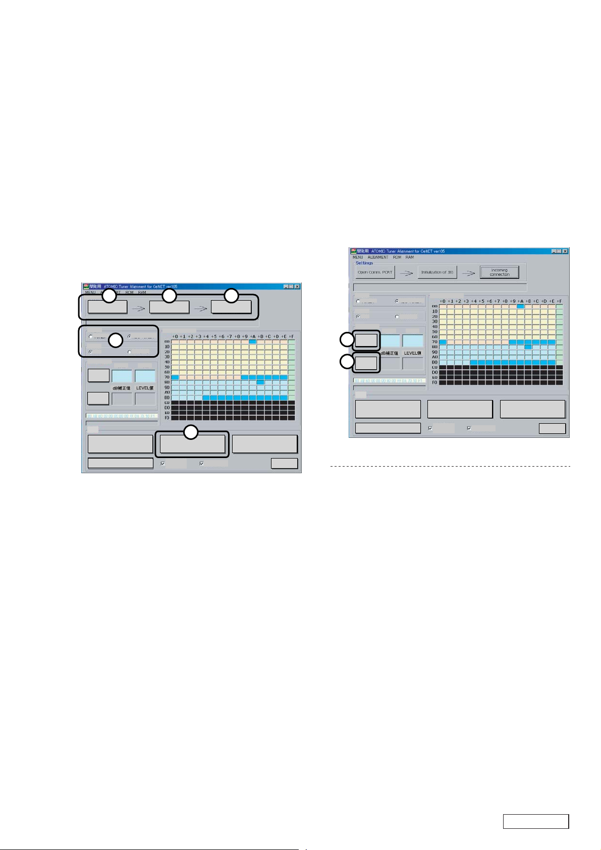
When this tool is executed, the VB6.0 run time is necessary.
Please download from web site and install it.
(http://www.vector.co.jp/soft/dl/win95/util/se188840.html)
< Measuring instrument>
* Adjustment software: AtomicAlign_Ver105 for development
* Ce-NET analyzer
* SG
<Setting of the prn file>
1. Install the adjustment software in the personal computer.
2. Connect the unit to the personal computer with the
CeNET analyzer.
3. Open the adjustment software in the computer, and turn
on the unit.
4. It is displayed on the screen " for development ", please
click " OK ". The tool starts.
<FM S-Meter adjustment>
1. Input 98.1MHz/20dBuV(30%MOD,400Hz) signal.
2. Click " Alignment " button, " SG Level 20dBuV " is
displayed.
3. Click " OK " after confirming SG is 20dB.
4. Input 40dBuV signal. Click " Alignment " button, " SG
Level 40dBuV " is displayed.
5. Click " OK " after confirming SG is 40dB.
6. When the adjustment is completed, " COMPLETED " is
displayed. Then click " OK " button.
7. Check the level whether the adjustment is normal. Set SG
to the arbitrary value between 20dB and 40dB, and click "
LV Check " button. If the dB correction value at that time
is +2dB/-2dB of a set value of SG, it is normally adjusted.
Settings
5 6 7
Open Comm. POR T
AREA
TUNER
8
BAND
FM
FM S-Meter
20dB
Alignment
LV Check
ROM
Data Read ALL Data Write(0x00-0xBF) Data Write(0x80-0xBF)
OK
RDS TUNER
MW(AM)
40dB
Initialization of JIG
ROM DATA MAP
Alignment
Protect
- Display (1) -
9
CheckSUM
Incoming
connection
All 0xFF
5. Click the " Open Comm.PORT " button of the display. The
communication of the personal computer and the
analyzer starts.
6. Click the " Initialization of JIG " button of the display. The
personal computer sends the command for operation of
the analyzer.
7. Click the " Incoming connection " button of the display.
The unit recognizes the external jig. The preparation
completes.
8. " AREA " and " BAND " are automatically set with the unit
if communicated. It is not necessary to set it.
9. Click the " Data Write(0x00-0xBF) " button, select the prn
file of " V8N9_PRN_eur_ver09 " (for Europe) " ,
V8N9_PRN_usa_ver06 " (for North America). The PRNdata is written in EEP-ROM of the unit.
When writing EEP-ROM in the unit is the initial setting, "
CS ERROR " is displayed, please continue it.
Confirm the unit or the setting when " CS ERROR " is
displayed excluding initialization.
AREA
2
7
TUNER
BAND
FM
FM S-Meter
Alignment
LV Check
ROM
RDS TUNER
MW(AM)
20dB
Data Read ALL Data Write(0x00-0xBF) Data Write(0x80-0xBF)
OK
40dB
ROM DATA MAP
Alignment
Protect
- Display (2) -
CheckSUM
<AM S-Meter adjustment>
1. Input 999kHz/30dBuV(30%MOD,400Hz) signal.
2. Click " Alignment " button, " SG Level 30dBuV " is
displayed.
3. Click " OK " after confirming SG is 30dB.
4. Input 50dBuV signal. Click " Alignment " button, " SG
Level 50dBuV " is displayed.
5. Click " OK " after confirming SG is 50dB.
6. When the adjustment is completed, " COMPLETED " is
displayed. Then click " OK " button.
7. Check the level whether the adjustment is normal as well
as FM adjustment. Set SG to the arbitrary value between
30dB and 50dB, and click " LV Check " button. If the dB
correction value at that time is +2dB/-2dB of a set value
of SG, it is normally adjusted.
8. After all the adjustments, select " END" of " MENU". And
press the reset button of the unit to set the data.
All 0xFF
- 13 -
NX700/NX700E
Page 14
Display section
< Panel PWB assembly adjustment (by CeNET command) >
* Setting of a signal generator output
VIDEO SIGNAL : 714mV / SYNCHRONIZED SIGNAL : 286mV
ITEM CHECK / ADJUST CONDITIONS
1. Power supply voltage
2. NAVI-RGB adjustment
1) RGB-GAIN(White-Black)
2) PHASE(Flicker)
3) H.V-POSITION
(Display position)
Confirm the power supply voltage
TP171 (LCD5V) : 5.0V +/-0.25V
TP162 (LCD3.3V) : 3.3V +/-0.15V
TP177 (VGL) : -12V +/-1.0V
TP173 (VGH) : +18.5V +/-1.0V
TP155 (LCD1.8V) : 1.8V +/-0.09V
TP151(OP-9V) : 9.0V +/-0.5V
Adjustment by automated command
(The adjustment of NAVI-RGB is a self adjustment in
the firmware of moses by CeNET command. )
* Input signal : NTSC
COMP : 10-steps wave
* Display : Composite screen
* BRT/COL/HUE : Initial setting
* DIMMER : 100%
* Tool : Digital volt meter
* Input signal : NTSC
NAVI test pattern :
Self adjustment pattern
3. NAVI-RGB check
Confirmation of self adjustment(2. NAVI-RGB
adjustment)
1) PHASE check
1dot monochrome line doesn't blot.
2) H.V-POSITION check
White frame line displays.
3) RGB-GAIN check
White-Black level of TP170(R),TP169(G) and
TP168(B)
White Black
* Input signal : NTSC
NAVI test pattern :
Self adjustment pattern
* Input signal : NTSC
NAVI test pattern :
Self adjustment pattern
* NAVI test pattern :
10-steps wave
* Same as the condition of item 1
* Tool : Oscilloscope
4. RGB-AMP voltage
(black-black level)
NX700/NX700E
2.8V +/-0.2V
WhiteBlack
Confirm the black-black level of TP170(R),TP169(G)
and TP168(B) will become 3.8V +/-0.2V.
White Black
3.8V +/-0.2V
WhiteBlack
- 14 -
* Input signal : NTSC
COMP : 10-steps wave
* Same as the condition of item 1
* Tool : Oscilloscope
Page 15
Adjust the black-white level of TP169(G) will become
2.8V +/-0.1V.
* Input signal : NTSC
COMP : 10-steps wave
* Same as the condition of item 1
* Tool : Oscilloscope
5. Contrast
(black-white level)
Color matrix:
BK2F_10_26h㫕2Eh
(2F4Ch㫕2F5Dh)
Initial setting:80
Adjustment range:0~FF
Display the waveform of TP169(G) on CH1 of an
oscilloscope.
Display the waveform of TP170(R) on CH2 of an
oscilloscope.
Adjust the waveform of TP170(R) to the same as the
waveform of TP169(G).
* Input signal : NTSC
COMP : 10-steps wave
* Same as the condition of item 1
* Tool : Oscilloscope(DC range)
8. White balance
(Red)
Color matrix:
Initial setting:80
Display the waveform of TP169(G) on CH1 of an
oscilloscope.
Display the waveform of TP168(B) on CH2 of an
oscilloscope.
Adjust the waveform of TP168(B) to the same as the
waveform of TP169(G).
* Input signal : NTSC
COMP : 10-steps wave
* Same as the condition of item 1
* Tool : Oscilloscope(DC range)
9. White balance
(Blue)
Color matrix:
Initial setting:80
Adjustment range:0~FF
Adjust the amplitude of waveform of TP172 to 5.5V
+/-0.1V.
* Input signal : NTSC
COMP : 10-steps wave
* Same as the condition of item 1
* Tool : Oscilloscope
10. VcomAC
Color matrix:
BK32_05Lh(320Ah)
Initial setting:B8
Adjustment range:0~FF
Confirm the waveform of TP169(G) that ten
gradation has come out. And confirm that it is the
3rd gradation is 1.6V +/-0.2V.
* Input signal : NTSC
COMP : 10-steps wave
* Same as the condition of item 1
* Tool : Oscilloscope
6. Gamma voltage
Set the range of CH1 and CH2 of an oscilloscope to
1V.
Display CH1 and CH2 in GND. And match it to GND.
* Input signal : NTSC
COMP : 10-steps wave
* Same as the condition of item 1
* Tool : Oscilloscope(DC range)
7. White balance setting
ITEM CHECK / ADJUST CONDITIONS
CH1
CH2
White Black
WhiteBlack
2.8V +/-0.1V
VCOM-AC LEVEL
Adjust the display flicker to the minimum by using a
flicker meter.
* Input signal : OSD test
pattern(Described in the left)
* Same as the condition of item 1
11. VcomDC
Color matrix:
BK32_04Lh(3208h)
Initial setting:50
Adjustment range:0~FF
- 15 -
NX700/NX700E
Page 16

<Touch panel calibration>
Make the unit to the calibration test display by the touch
panel calibration command or the touch panel operation.
Touch panel operation for calibration test display
1. Push the touch key of "T-PNL" in the display of
version/various.
It changes to the touch panel calibration display.
How to operate touch panel calibration
1. Touch the center of yellow frame under the left with a thin
rod. The color changes into pink.
2. Touch the center of yellow frame upper the right with a
thin rod. The color changes into pink.
3. Touch the center of pink frame under the left with a thin
rod. The color changes into light blue.
4. Touch the center of pink frame upper the right with a thin
rod. The color changes into light blue.
5. Push [VOL-] button. The data is recorded in E2PROM.
6. Turn off ACC. The test mode ends.
NX700/NX700E
- 16 -
Page 17
EXPLANATION OF IC
051-3579-90 S-1112B15MC-L6ATFG
051-6934-90 Apple MFI341S2313 iPod Authentication
MODE1/SPI_nSS
Terminal Description
pin 1: MODE1 / SPI_nSS : IN : Reset:selects communication mode. /
pin 2: NU : - : Not in use.
pin 3: nRESET :IN : CP reset. (active low)
pin 4 : VCC : - : Positive voltage supply.
pin 5 : VSS : - : Negative voltage supply.
pin 6 : I2C_SCL /SPI_SIMO : I/O : I2C mode: I2C clock. / SPI mode:
pin 7 : I2C_SDA / SPI_SOMI : I/O : I2C mode: I2C DATA. / SPI mode:
pin 8: MODE0 / SPI_CLK : IN : Reset:selects communication mode. /
IC503(Main PWB) NEC uPD70F3356GJ Audio CPU
[NOTE] When these IC are exchanged, it is necessary to write the pro-
gram because the program is not written in this IC.
Please note that the ROM data vary for each model program.
Terminal Description for QY-5014B-A,QY-5015E-A
pin 1: A Vref 0 : IN: Analog reference voltage.
pin 2 : A VSS : - : Analog ground.
pin 3: E2P_SDA :I/O: EEP serial data input / output.
pin 4: E2P_SCL : O : EEP serial clock output.
pin 5: A Vref 1 : IN: Analog reference voltage.
pin 6: RDS_CK :IN : Clock pulse input from RDS decoder.
pin 7: AV_ON :O : Power supply control signal output.
pin 8: FLM : IN : Flash Mode. H = Flash write.
pin 9 : VDD +3.3V : - : Positive voltage supply.
pin 10: REG C : - : Capacitor connection.
pin 11: VSS : - : Negative voltage supply.
pin 12: X IN : IN : The crystal connection.
pin 13: X OUT : O : The crystal connection.
pin 14: RESET :IN : Reset signal input.
pin 15: NU : - : Not in use.
pin 16: NU : - : Not in use.
pin 17: NU : - : Not in use.
pin 18: B/U 9V DET : IN : B/U 9V detection signal intput.
pin 19: B/U 6V DET : IN : B/U 6V detection signal intput.
pin 20: NU : - : Not in use.
pin 21: CATS_DET :IN: CATS detection signal input. L = ON
pin 22 : Tuner DA :I/O: Tuner serial data.
Low-saturation Voltage Regulator 1.5V
1
V_IN
GND
ON/OFF
NU
nRESET
VCC
54V_OUT
2
3
1
2
3
4
(top view)
NU
8
MODE0/SPI_CLK
7
I2C_SDA/SPI_SIMI
6
I2C_SCL/SPI_SIMO
5
Vss
SPI mode: SPI clock.
master-to-slave data.
slave-to-master data.
SPI mode:SPI clock
Coprocessor
pin 23 : Tuner CK : O : Tuner clock output.
pin 24: NU : - : Not in use.
pin 25: MA-NAVI : O : AUDIO-NAVI TX serial data output.
pin 26: NAVI-MA : IN: NAVI-AUDIO RX serial data input.
pin 27: NU : - : Not in use.
pin 28: NU : - : Not in use.
pin 29: M_PLS :IN : Motor Pulse input.
pin 30: NU : - : Not in use.
pin 31: BUS+ : O : BUS data output.
pin 32: BUS- :IN : BUS data input.
pin 33: VSS : - : ground.
pin 34: VDD +3.3V : - : Positive voltage supply.
pin 35: USB_SDA :I/O: USB serial data.
pin 36: USB_CK : O : USB clock output.
pin 37: MTR_1F : O : Motor control output.
pin 38: MTR_1R : O : Motor control output.
pin 39: NU : - : Not in use.
pin 40: NU : - : Not in use.
pin 41: NU : - : Not in use.
pin 42: NU : - : Not in use.
pin 43: NAVI_SYS_ACC : O : NAVI unit, the output signal to the ACC.
pin 44: USB_RESET : O : USB reset signal output.
pin 45: USB_ACC : O : Start control pin USB microcontrollers.
pin 46: USB_REQ : IN : Request control pin USB microcontrollers.
pin 47: AMP_STB : O : Standby signal output to the amplifier.
pin 48: AMP_MUTE : O : The amplifier mute signal output.
pin 49: 2ZONE-SENS1 : O : 2ZONE SENS1 input AUX terminal for
switching output. (Lo=L / Mid=L / Hi=H)
pin 50: 2ZONE-SENS2 : O : 2ZONE SENS2 input AUX terminal for
switching output. (Lo=L / Mid=L / Hi=H)
pin 51: VOL_UP :IN : Volume up signal input.
pin 52: VOL_DOWN : IN : Volume down signal input.
pin 53 : IR : IN : IR signal input.
pin 54: VOL_SDA :I/O: I2C serial data input/output to the volume.
pin 55: VOL_SCL : O : I2C serial clock output to the volume.
pin 56: NU : - : Not in use.
pin 57: NAVI_MONI :IN: NAVI connection detection (H=NAVI con-
nection / L=NAVI disconnected)
pin 58: NAVI_RESET : O : NAVI forced to RESET (L=Reset Output /
H=Normal operation)
pin 59: DVD_MA :IN: Asynchronous data received from the dvd
mech.
pin 60: MA_DVD : O : Asynchronous data transmission to the
dvd mech.
pin 61: MOS_SDA :I/O: I2C serial data input/output to the Moses.
pin 62: MOS_SCL : O : I2C serial clock output to the Moses.
pin 63: W_REMCOM :IN:
Handle for the remote control input
pin 64: NU : - : Not in use.
pin 65: SOURCE :IN : Source key input.
pin 66: NU : - : Not in use.
pin 67: BEEP : O : Beep output.
pin 68: TP_MA : IN: Serial data input from the touch panel
Moses.
pin 69: NU : - : Not in use.
pin 70: TP_SCK :I/O:Serial clock output from the touch panel
Moses.
pin 71: MOS_RESET : O : Moses reset signal output.
pin 72: W P : O : Write protect output. (usually = L ,F-ROM
writing = H)
pin 73: RDS_DATA :IN: RDS data input.
pin 74: NU : - : Not in use.
pin 75: MOS_BUF_DET :IN : Moses in the memory buffer was full at
the time, to inform the master.
pin 76: MOS_RST_DET :IN : Moses reset detection input.
- 17 -
NX700/NX700E
Page 18

pin 77: 2ZONE_A : O : 2ZONE_A source switching terminal (AUX
= H ,DVD = L, USB = H, 2ZONE OFF =
L)
pin 78: 2ZONE_B : O : 2ZONE_B source switching terminal (AUX
= H ,DVD = H, USB = L, 2ZONE OFF =
L)
pin 79: NU : - : Not in use.
pin 80: NU : - : Not in use.
pin 81: PANEL_ON : O : LCD panel power on signal output.
pin 82: FAN_ON :O : Fan power on signal output.
pin 83 F_SEL : O : When DD-CON and RADIO, oscillation fre-
quency select.
pin 84: NU : - : Not in use.
pin 85: NU : - : Not in use.
pin 86: NU : - : Not in use.
pin 87: RDS_TEST1 : O : RDS output for the driving test.
pin 88: RDS_TEST2 : O : RDS output for the driving test.
pin 89: RDS_TEST3 : O : RDS output for the driving test.
pin 90: NU : - : Not in use.
pin 91: NU : - : Not in use.
pin 92: NU : - : Not in use.
pin 93: NU : - : Not in use.
pin 94: NU : - : Not in use.
pin 95: NU : - : Not in use.
pin 96: NU : - : Not in use.
pin 97: NU : - : Not in use.
pin 98: NU : - : Not in use.
pin 99: USA/3rd : IN : H = North America, L = 3rd area
pin100: NTSC/PAL : IN: L = NTSC, H = PAL
pin101: NOISE_TEST : IN : Radio terminal to verify the performance
test. (Usually set state = L)
pin102: BRAZ/OTHER : IN : H = Brazil, L = Other
pin103: BVSS : IN: ground.
pin104 BVDD : IN: Positive voltage supply. (+3.3V)
pin105: ILL DET : IN: Illumination detect signal input.
pin106: AV/ILL_ON : O : Select signal output to the AV_ON and
ILL_ON signal input selector.
pin107: ILL_ON : O : Illumination ON signal output.
pin108: BLK_LED : O : LED Blinking signal output.
pin109: NU : - : Not in use.
pin110: NU : - : Not in use.
pin111: NU : - : Not in use.
pin112: NU : - : Not in use.
pin113: NU : - : Not in use.
pin114: NU : - : Not in use.
pin115: SOFT_TEST1 : O : Soft test port.
pin116: SYS_ACC : O : ACC detection signal output.
pin117: NU : - : Not in use.
pin118: NU : - : Not in use.
pin119: NU : - : Not in use.
pin120: NU : - : Not in use.
pin121: DAC_RST_DVD : O : External DVD RESET output for the DAC-
IC.
pin122: TEST_MODE : O : For the test. Production output port.
pin123: OP/CL : IN: Open/close detection signal input.
pin124: TEL_IN :IN : Telephone interrupt signal input.
pin125: SD_DET2 :IN : SD Card detection. Fully inserted SD = L,
SD insert or incomplete without = H
pin126: SD_DET1 :IN : Insert SD detected, L = no SD, H = SD
in (including mid-position)
pin127: SYS_MUTE : O : System muting signal output.
pin128: SUB_MUTE :O : Sub-zone audio mute signal output.
pin129: NU : - : Not in use.
pin130: FAN_TEMP : IN: Input of the internal ADC to detect the
temperature.
NX700/NX700E
pin131: NU : - : Not in use.
pin132: DVD_ON2 : O : Mechanical power 5V (Analog) ON signal
terminal.
pin133: DVD_ON3 : O : M e chanical power 8V (Servo) ON signal
terminal.
pin134: DVD_RST : O : Reset signal output for DVD mechanism.
pin135: CSN : O : Video selector to communication line out-
put.
pin136: CCLK : O : Video selector to communication line out-
put.
pin137: CDTI : O : Video selector to communication line out-
put.
pin138: VIDEO_RST : O : RESET line to the Video selector.
pin139: BACK GEAR :IN : The back gear signal input. L = back.
pin140 PKB :IN : Parking brake signal input. Auto antenna
control signal output.
pin141: AMP_REM DET : IN : Remote output short circuit detection.
pin142 AMP_REM : O : External amp control signal output.
Shorts = L
pin143: A_ANT :O : Auto antenna control signal output.
Shorts = L, Radio on = H
pin144 ACC_IN :IN: ACC detection signal intput.
052-3409-30 Toshiba TMP92FD28AFG Controller
Terminal Description
pin 1: RESET :IN : Reset signal input.
pin 2 : BU DET : IN: Backup detection signal input.
pin 3: ACC DET : IN : ACC detection signal input.
pin 4: NU : - : Not in use.
pin 5 : ST REQ : IN : Request signal input.
pin 6 : D VDD : - : Positive voltage supply for the digital sec-
tion.
pin 7 : XT 1 : IN : 3.14MHz crystal connection. (sub-clock)
pin 8 : XT 2 : O : 3.14MHz crystal connection. (sub-clock)
pin 9 : PW E : O : External power supply control output.
pin 10: D VSS : - : Digital ground.
pin 11: D VDD : - : Positive voltage supply for the digital sec-
tion.
pin 12: Reg V out 1 : O : regulator 1.5V output.
pin 13: VDD : - : Positive voltage supply.
pin 14: VDD : - : Positive voltage supply.
pin 15: Reg V out 2 : O : regulator 1.5V output.
pin 16: D VDD : - : Positive voltage supply for the digital sec-
tion.
pin 17: D VSS : - : Digital ground.
pin 18 : P ON 3 : O : Power ON signal output.
pin 19 : P ON 4 : O : Power ON signal output.
pin 20: NU : - : Not in use.
pin 21: NU : - : Not in use.
pin 22: NU : - : Not in use.
pin 23: NU : - : Not in use.
pin 24: NU : - : Not in use.
pin 25: NU : - : Not in use.
pin 26: D VSS : - : Digital ground.
pin 27: D VDD : - : Positive voltage supply for the digital sec-
tion.
pin 28: REQ O : O : Request signal output.
pin 29: NU : - : Not in use.
pin 30: NU : - : Not in use.
pin 31: NU : - : Not in use.
pin 32: NU : - : Not in use.
pin 33 : P ON 2 : O : Power ON signal output.
pin 34: NU : - : Not in use.
- 18 -
Page 19

pin 35: NU : - : Not in use.
pin 36 : IC Ready In :IN : Authentication system ready input.
pin 37 : IC Reset Out : O : Authentication system reset output.
pin 38: NU : - : Not in use.
pin 39: NU : - : Not in use.
pin 40: NU : - : Not in use.
pin 41: NU : - : Not in use.
pin 42: NU : - : Not in use.
pin 43: NU : - : Not in use.
pin 44: D VSS : - : Digital ground.
pin 45: D VDD : - : Positive voltage supply for the digital sec-
tion.
pin 46: NU : - : Not in use.
pin 47: NU : - : Not in use.
pin 48: NU : - : Not in use.
pin 49: NU : - : Not in use.
pin 50: NU : - : Not in use.
pin 51: NU : - : Not in use.
pin 52: NU : - : Not in use.
pin 53: NU : - : Not in use.
pin 54: NU : - : Not in use.
pin 55: NU : - : Not in use.
pin 56: NU : - : Not in use.
pin 57: NU : - : Not in use.
pin 58 : DSP ACK : IN : DSP acknowledge.
pin 59 : DSP LP : O : DSP latch pulse output.
pin 60 : DSP CS : O : Chip select signal output to the DSP.
pin 61 : DSP RESET : O : DSP reset pulse output.
pin 62: D VSS : - : Digital ground.
pin 63: D VDD : - : Positive voltage supply for the digital sec-
tion.
pin 64: NU : - : Not in use.
pin 65: NU : - : Not in use.
pin 66 : HSSW :IN : Mode set.
pin 67: HSSW 2 : IN : Mode set.
pin 68: SRAM STNDO : O : SRAM standby output.
pin 69: BOOT : IN: Flash Memory Write mode selection.
pin 70: NU : - : Not in use.
pin 71 : LR CK : O : LR clock output.
pin 72: A M 1 : IN : Function Mode.
pin 73 : X 2 : - : Main clock.
pin 74: D VSS : - : Digital ground.
pin 75 : X 1 : - : Main clock.
pin 76: D VDD : - : Positive voltage supply for the digital sec-
tion.
pin 77 : USB OC :IN : USB over current.
pin 78: USB P ON : O : USB opwer on.
pin 79: USB D+ : - : USB positive line.
pin 80: USB D- : - : USB negative line.
pin 81: A M 0 : IN : Function Mode.
pin 82 : DSP REQ : IN: DSP request input.
pin 83: D VSS : - : Digital ground.
pin 84: IC Data Out : O : Authentication system data output.
pin 85: IC Data In : IN: Authentication system data input.
pin 86: IC CK : O : Authentication system clock output.
pin 87 : MI SO : O : Serial data output to the DSP.
pin 88 : MI SI : IN : DSP serial data input.
pin 89: MI CK : O : Serial clock output to the digital signal
processor.
pin 90 : I2C SDA :I/O: I2C serial data input/output.
pin 91 : I2C CK : IN : I2C serial clock input.
pin 92 : AUDIO CK : O : Audio data bit clock output.
pin 93 : AUDIO DO : O : Audio data output.
pin 94 : GATE : O : Gate signal output.
pin 95: D VDD : - : Positive voltage supply for the digital sec-
tion.
pin 96: NU : - : Not in use.
pin 97: NU : - : Not in use.
pin 98: NU : - : Not in use.
pin 99: NU : - : Not in use.
pin100: D VS S : - : Digital ground.
052-7094-10 MX25L1605DM1-12G 16M bit Serial FLASH ROM
Terminal Description
Please note that the ROM data vary for each model program.
pin 1 : HOLD : IN : Hold,to pause the device without deselect-
ing the device.
pin 2 : VCC : - : Positive supply voltage.
pin 3: NU : - : Not in use.
pin 4: NU : - : Not in use.
pin 5: NU : - : Not in use.
pin 6: NU : - : Not in use.
pin 7 : CS : IN : Chip Select.
pin 8: SO : - : The serial data output
pin 9 : WP : - : Write protection.connect to GND.
pin 10: GND :Ground.
pin 11: NU : - : Not in use.
pin 12: NU : - : Not in use.
pin 13: NU : - : Not in use.
pin 14: NU : - : Not in use.
pin 15 : SI :The serial data input.
pin 16: S C LK : - : Clock input.
- 19 -
NX700/NX700E
Page 20
Y
Y
(B)(1)
(B)(2)
(C)(4)
ASSEMBLY
Y
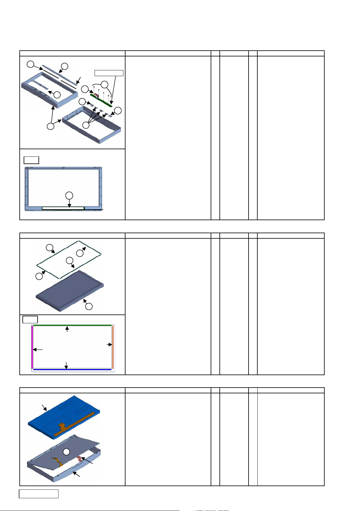
1. Processing of Panel ASSY
1-1. Installation of Panel PWB-B (1)
WORKING DIAGRAM WORKING PROCESS WORKING POINT
No. PARTS CODE
Q'T
A
×2
stick it on Escutcheon B 370-6443-00 1
(Fig.1)
C
gate side
J
B
I
G
E
F
Panel PWB-B
H
basic line
1. Peel off the Double face from a sheet, A 347-8742-00 2
and peel off the separator.
2. Fit the gate side of the badge C 378-0559-03 1 * No floating,
to the hole of Escutcheon. (NX700) bending and warping.
D
3. Attach the Reset button on Escutcheon. D 382-9177-00 1
4. Attach the IR filter on Escutcheon. E 335-8654-00 1
5. Attach the three buttons(G) F 382-9176-00 3
on Escutcheon.
6. Unlock Flex-socket of Panel PWB-B, G 039-3225-00 1
insert FPC, and lock by hand.
7. Attach Panel PWB-B
on the processed Escutcheon,
fix the pad screw. H 778-2004-01 4
8. Attach the film on Panel PWB-B. (Fig.1) I 347-8743-00 1 * Put it based on the wall
9. Peel off the sheet key from a sheet, J 382-9175-00 1
confirm the top and bottom,
and stick it on Escutcheon.
C 378-0559-04 1
(NX700E)
1-2. Installation of LCD (1)
WORKING DIAGRAM WORKING PROCESS WORKING POINT
No. PARTS CODE
Q'T
of Escutcheon.
bring LCD close to a ionaizer.
(Fig.1)
C
B
C
B
A
(C)(3)
1. Clip the grounded tip of FPC of LCD, A 379-0478-00 1
And peel off the protection sheet
slowly in the wind.
2. Peel off the spacer(B)(1) from the sheet B 347-8741-00 1 * The sticking portion(B)(1)
and stick it on LCD. (Fig.1)
3. Peel off the spacer(B)(2) from the sheet B 347-8741-00 1 * The sticking portion(B)(2)
and stick it on LCD. (Fig.1)
4. Peel off the spacer(C)(3) from the sheet C 347-8740-00 1 * The sticking portion(C)(3)
and stick it on LCD. (Fig.1)
5. Peel off the spacer(C)(4) from the sheet C 347-8740-00 1 * The sticking portion(C)(4)
and stick it on LCD. (Fig.1) * Stick it on the center of
1-3. Installation of LCD (2)
WORKING DIAGRAM WORKING PROCESS WORKING POINT
processed
LCD
processed Escutcheon below.
A
FPC of
Panel PWB-B
processed
Escutcheon
1. Turn the front side of
2. Attach touch panel A 013-9723-00 1 * Put the touch panel
on processed Escutcheon. along the wall in Escutcheon.
* Bend Flex PWB naturally.
3. Draw out Flex-PWB of the touch panel * Do not pinch Flex-PWB
and FPC of Panel PWB-B. of the touch panel
Attach processed LCD and FPC of Panel PWB-B.
on processed Escutcheon.
No. PARTS CODE
LCD metallic frame.
Q'T
* Attach from the upper part
of the touch panel.
* Do not pinch Flex-PWB of
Panel PWB-B.
NX700/NX700E
- 20 -
Page 21
1-4. Installation of LCD (3)
No. PARTS CODE
Q'T
Y
1. Peel off the separator from Earth plate(A) A 331-3038-00 1
and stick it on LCD holder(B). (Fig.1) B 331-4803-00 1
2. Attach processed LCD to * Fit at 8 tab.
processed Escutcheon
after the blow of air. (Fig.2)
3. Insert Lead(2P) on the LCD side
in the socket of LCD PWB. (Fig.3)
4. Attach LCD PWB on LCD holder * Twist tabs according to
while holding Flex-PWB on the LCD side, the silk print.
and twist the 2 tabs.
(Fig.4)
WORKING DIAGRAM WORKING PROCESS WORKING POINT
B
A
LCD-PWB
processed
Escutcheon
(Fig.1)
(Fig.2)
(Fig.3) (Fig.4)
(A)
(B)
LCD PWB
2P lead
twist the tab
tab
tab tab tab
tab
tab
tab
tab
twist the tab
Y
1-5. Installation of LCD (4)
Y
WORKING DIAGRAM WORKING PROCESS WORKING POINT
No. PARTS CODE
Q'T
of LCD PWB.
Flex-socket
(J102)
Flex-socket
(J104)
Flex-socket
(J105)
1. Unlock Flex-socket (J102,J104,J105)
2. Insert FPC of Panel PWB-B * Insert it while holding Flex-PWB.
into Flex-socket(J105) of LCD PWB, * Do not never touch it
and lock it. after locking.
3. Insert Flex-PWB of LCD * Insert it while holding Flex-PWB.
into Flex-socket(J104) of LCD PWB, * Do not never touch it
and lock it. after locking.
Flex-PWB of
touch panel
1-6. Installation of Rear cover (1)
apply grease on the shaft.
Flex-PWB of
LCD
WORKING DIAGRAM WORKING PROCESS WORKING POINT
C
B
apply grease
FPC of
Panel PWB-B
E
D
apply grease
4. Insert Flex-PWB of touch panel * Insert it while holding Flex-PWB.
into Flex-socket(J102) of LCD PWB, * Do not never touch it
and lock it. after locking.
5. Arrange FPC of Panel PWB-B
under LCD PWB.
1. Turn the left of rear cover to up, A 331-4804-10 1
2. Insert the spring and the roller B 750-6746-10 1
in shaft(left side) of rear cover. C 335-7074-00 1
3. Turn the right of rear cover to up,
apply grease on the shaft.
4. Insert the spring and the roller D 750-6746-10 1
in shaft(right side) of rear cover. E 335-7074-00 1
No. PARTS CODE
Q'T
A
- 21 -
NX700/NX700E
Page 22

1-7. Installation of Rear cover (2)
Y
(
)
(
)
Y
Y
WORKING DIAGRAM WORKING PROCESS WORKING POINT
3 times. without caught.
B
B
1. Push the roller of processed rear cover * Confirm that operates smoothly
No. PARTS CODE
(Right and left two portions for each)
processed
rear cover
A
2. Confirm FPC(J102, J104, J105)
and 2P lead.
3. Stick heat rubber on the upper side A 345-6395-00 1
of IC103 of processed Escutcheon.
Q'T
4. Attach processed rear cover on
processed Escutcheon,
fix it with screw(B). B 780-2604-50 4
FPC
(J102)
(A)
processed
Escutcheon
2P lead
FPC
J105
FPC
J104
1-8. Installation of Escutcheon (1)
WORKING DIAGRAM WORKING PROCESS WORKING POINT
A B
1. Fix the upper side of
No. PARTS CODE
processed Escutcheon with screw(A). A 780-2003-03 3
2. Fix the lower side of
processed Escutcheon with screw(B). B 780-2003-03 2
processed
Escutcheon
Q'T
2. Processing of Main unit
2-1. Processing of DVD mechanism
WORKING DIAGRAM WORKING PROCESS WORKING POINT
(3)
F
on the Main PWB holder. B 312-0505-01 1
(2)
dowel
dowel
E
(4)
(1)
F
(5)
G
dowel
H
1. Put lower chassis A 331-4807-00 1
2. Put the insulator on lower chassis. (Fig.1) C 347-8504-00 1
3. Attach DVD mechanism D 929-2170-80 1
on processed lower chassis.
I
No. PARTS CODE
4. Attach upper chassis E 312-0506-00 1 * Fit at 4 dowels.
on processed DVD mechanism,
D
B
A
C
K
J
Unlock
Flex-socket of
DVD mechanism
dowel
(7)
(8)
(6)
dowel
and fix it with machine screw(F). F 714-2604-8B 5 * Follow screw sequence. (1 to 5)
5. Put the spacer on upper side G 347-8760-00 1
of upper chassis.
K
6. Turned the front side of
processed DVD mechanism below,
and fix it with machine screw(H). H 714-2604-8B 2
7. Turned the upper side of
processed DVD mechanism below,
and fix it with machine screw(I). I 714-2604-8B 2
8. Unlock Flex-socket of DVD mechanism.
9. Turned the rear side of
(Fig.1)
basic line
basic line
processed DVD mechanism below.
10. Attach front plate, J 309-1911-00 1 * Fit at 2 dowels.
and fix it with machine screw(K). K 714-2604-8B 3 * Follow screw sequence. (6 to 8)
Q'T
11. Unlock Flex-socket of DVD mechanism.
NX700/NX700E
- 22 -
Page 23

2-2. Installation of MAIN PWB
Y
g
t
).
s
y
>
(1)
(2)
(3)
(4)
WORKING DIAGRAM WORKING PROCESS WORKING POINT
No. PARTS CODE
Q'T
A
on processed DVD mechanism.
tab
tab
tab
A
processed
Main PWB
processed
DVD mechanism
tab
1. Attach processed Main PWB * Fit at 4 tabs.
2. Fix it with IT screw(A). A 780-2604-50 4 * Follow screw sequence. (1 to 4)
< Only NX700E(QY-5015E-A) >
3. Put ANT-lead of Main PWB
on the upper chassis.
The point is temporarily stopped
with the masking tape. (Fig.1)
4. Confirm that the direction of dashin
C
B
of ANT-lead from Main PWB
and the silk print of PWB
are the same direction.
dowel
Attach it from the
front plate side
5. Insert FPC on the Main PWB side
in the socket of the DVD mechanism.
6. Check an insertion and a lock state
of FFC of socket(J401) of Main PWB.
(Fig.1)
< Only NX700E(QY-5015E-A) >
㫄㪸㫊㫂㫀㫅㪾㩷㫋㪸㫇㪼
ANT-lead
Insert FPC
on the socket of
ANT-lead
DVD mechanism.
ou
ANT-lead
7. Attach side chassis R B 312-0504-00 1 * Attach it from the front plate side
on the right side of Main unit, diagonally.
and fix it with machine screw(C
C 714-2604-8B 2 * Fit at 2 dowel
on front plate side,
on upper chassis.
NX700E(QY-5015E-A)
< Onl
* Attach the side chassis R,
confirm ANT-lead doesn't crowd.
- 23 -
NX700/NX700E
Page 24

Y
A
t
A
(4)
(3)
(2)
(1)
2-3. Installation of Slide mechanism
Y
g
s
dowe
dowe
dowe
WORKING DIAGRAM WORKING PROCESS WORKING POINT
B
and fix it with machine screw(B). B 714-2604-8B 2 diagonally.
A
1. Attach side chassis L on Main unit, A 312-0503-00 1 * Attach it from the front plate side
No. PARTS CODE
2. Attach earth plate on side chassis R C 331-4870-00 1 * Fit at 1 tab.
of Main unit, and fix it
processed
Slide mechanism
l
with machine screw(D). D 714-2604-8B 1
3. Attach processed Slide mechanism * Fit at 4 dowels.
on Main unit.
4. Turn the unit to the left,
D
C
and check the fittin
on Slide mechanism.
Fix it with machine screw(E). E 780-2604-51 2
at 2 dowel
5. Turn the unit to the right,
TM101
TM102
and check the fitting at 2 dowels
on Slide mechanism.
Fix it with machine screw(F). F 780-2604-51 2
Q'T
* Fit at 2 dowels
on front plate side,
on upper chassis.
E
E
F
w
l
2-4. Installation of Navi PWB
WORKING DIAGRAM WORKING PROCESS WORKING POINT
< Only NX700E(QY-5015E-A) >
B
㫋㪸㪹
B
㫋㪸㪹
l
Insert
NT-lead
l
No. PARTS CODE
Q'T
< Only NX700E(QY-5015E-A) >
1. Peel off the masking tape
temporarily stopped
with ANT-lead of Main PWB.
B
2. Attach NAVI-PWB-ASSY on Main unit. A ----------- 1 * Fit at 2 tabs.
3. Fix it with IT screw(B). B 780-2604-50 4 * Follow screw sequence. (1 to 4)
A
< Only NX700E(QY-5015E-A) >
4. Insert ANT-lead of Main PWB
in the socket of NAVI-PWB-ASSY.
5. After inserting it, rotate the terminal
of ANT-lead lightly as follows.
NX700/NX700E
Main uni
NT-lead
- 24 -
Page 25

2-5. Installation of Rear cover
Y
Y
(8P)
y
(8P)
e
)
WORKING DIAGRAM WORKING PROCESS WORKING POINT
No. PARTS CODE
Q'T
C
1. Fit the metal fittings part
of the USB lead of Main PWB
and the Main PWB holder
with the machine screw(A). A 714-2604-8B 1
2. Attach rear cover on Main unit, B 307-0738-01 1 * Fit at 2 dowels.
and fix it with machine screw(C). C 714-2604-8B 10 * Follow screw sequence. (1 to 10)
dowel
B
(Fig.1)
(C)(2)
Main unit
A
dowel
(C)(3)
dowel
(C)(4)
(C)(5)
2-6. Installation of Front plate
WORKING DIAGRAM WORKING PROCESS WORKING POINT
Socket(flip lock)
: NAVI-PWB-ASSY
and fix it with machine screw(B)(C). B 780-2604-50 2
Socket (J502)
1. Attach ANT-PWB on the front plate, A ----------- 1
2. Insert BT-ANT lead in ANT receptacle D 092-2239-01 1
of ANT-PWB-ASSY.
3. Unlock the following socket.
* J5001 : SLIDE-PWB
* J382 : MAIN-PWB
* J452 : MAIN-PWB
* J502 : MAIN-PWB
* Socket(flip lock) : NAVI-PWB-ASSY
4. Insert FPC(24P) in the socket(J382) E 816-3041-55 1
of MAIN-PWB.
Insert the other side of FPC(24P)
㪻㫆㫎㪼㫃
㪻㫆㫎㪼㫃
㪻㫆㫎㪼㫃
Socket (J452)
㪻㫆㫎㪼㫃
㪻㫆㫎㪼㫃
㪻㫆㫎㪼㫃
in the socket of NAVI-PWB-ASSY,
and lock by the hands.
E
F
5. Insert FPC(8P) in the socket(J5001) F 816-3040-55 1
of Slide PWB, and lock.
No. PARTS CODE
C 714-2604-8B 4
Q'T
(C)(10)
(C)(9)
(C)(1)
dowel
(C)(8)
(C)(7)
(C)(6)
A
D
B
C
Socket (J382)
(Fig.1)
Socket (J5001)
6. Insert the other side of FPC
in the socket(J502) of Main PWB,
and lock b
the hands.
7. Process the part of the rest of FFC
as follows.
8P-FFC
8. Insert BT-ANT lead in ANT receptacl
of NAVI-PWB-ASSY. (Fig.1
- 25 -
NX700/NX700E
Page 26

Y
(2)
2-7. Installation of Inner Escutcheon
Y
Y
y
e
g
WORKING DIAGRAM WORKING PROCESS WORKING POINT
B
of the front side on Main unit,
A
㪻㫆㫎㪼㫃
1. Insert FPC(A) in Flex-socket A 039-3448-00 1 * Fit at 2 dowels.
and lock by the hands.
2. Fix it with IT screw(B). B 780-2604-50 1
processed
Inner Escutcheon
C
3. Attach it putting the tab of lower side of * Fit at 4 tabs of lower side.
processed Inner Escutcheon
on Main unit.
4. Fix it with screw(C). C 780-2604-52 4
㪤㪸㫀㫅㩷㫌㫅㫀㫋
No. PARTS CODE
Q'T
2-8. Installation of Upper case
WORKING DIAGRAM WORKING PROCESS WORKING POINT
(4) (1)
B
and fix it with machine screw(B). B 714-2604-8B 4 Inner Escutcheon
B
(3)
1. Attach upper case on Main unit, A 310-1831-02 1 * Fit at convex part of
No. PARTS CODE
Q'T
and hole of upper case.
* Follow screw sequence. (1 to 4)
hole
Convex part
2-9. Installation of Panel ASSY
WORKING DIAGRAM WORKING PROCESS WORKING POINT
C
in the ditch on the Inner Escutcheon
㪤㪸㫀㫅㩷㫌㫅㫀㫋
B
㪝㫃㪼㫏㪄㪧㪮㪙
A
㪝㫃㪼㫏㪄㫊㫆㪺㫂㪼㫋
㪝㫃㪼㫏㪄㪧㪮㪙
1. Set the Slide roller of PANEL-ASSY A ----------- 1
one by one side, put on Panel.
2. Unlock Flex-socket of
rear side of Panel.
Insert Flex-PWB of Main unit in it,
and lock.
3. Attach Panel cover on Panel, B 039-3502-00 1
and fix it with special screw(C). C 716-1851-00 2
4. Turn it so that the right side of Main unit
ma
become upper sid
while holding PANEL.
No. PARTS CODE
Q'T
5. Align the slide rail with the screw hole
E
D
G
F
of PANEL, attach the bush(D) D 335-7903-00 1
and fix with special screw(E). E 716-3577-00 1
6. Turn it so that the left side of Main unit
may become upper side.
n the slide rail
7. Ali
with the screw hole of PANEL,
attach the bush(F) F 335-7903-00 1
and fix with special screw(G). G 716-3577-00 1
NX700/NX700E
- 26 -
Page 27

EXPLODED VIEW/PARTS LIST
Panel assy section
20
19
3
4
3
9
8
6
Panel PWB-A
(From Main PWB)
21
32
33
30
21
20
30
18
5
7
3
31
17
1
25
23
10
2
11
24
1
14
15
12
25
Panel PWB-B
13
Note) Some parts depend on each model. The model name is specified in the description.
1 ----------- PANEL PWB 1
2 074-2236-65 OUTLET SOCKET(15P) 1
3 073-0762-90 TERMINAL 4
4 076-0529-02 PLUG(LCD 2P) 1
5 074-2219-54 OUTLET SOCKET(T/P 4P) 1
6 074-2225-66 OUTLET SOCKET(SW FPC 16P) 1
7 074-2226-80 OUTLET SOCKET(30P) 1
8 074-2233-50 OUTLET SOCKET(50P) 1
9 331-4805-00 SHIELD CASE 1
10 370-6443-00 ESCUTCHEON 1
11 335-8654-00 IR-FILTER 1
12 378-0559-03 BADGE : NX700 1
13 382-9175-00 SHEET KEY 1
14 382-9176-00 BUTTON(VOL/SRC) 3
15 382-9177-00 BUTTON(RESET) 1
16 013-9723-00 SWITCH(T/P) 1
17 379-0478-00 INDICATOR(LCD) 1
378-0559-04 BADGE : NX700E 1
16
29
29
26
28
27
NO. PART NO. DESCRIPTION Q'TYNO. PART NO. DESCRIPTION Q'TY
18 331-4803-00 LCD HOLDER 1
19 331-4804-10 REAR-CVR 1
20 335-7074-00 ROLLER 2
21 750-6746-10 ROLLER SPRING 2
22 331-3038-00 EARTH PLATE 1
23 039-3225-00 FPC(SW-LCD) 1
24 347-8742-00 DOUBLE FACE(BADGE) 2
25 780-2003-03 SPECIAL SCREW(M2x3 LOCK) 5
26 778-2004-01 PAD SCREW(M1.7x5) 4
27 347-8743-00 FILM 1
28 347-8740-00 SPACER(U/D) 2
29 347-8741-00 SPACER(L/R) 2
30 780-2604-50 IT SCREW(M2.6x4) 4
31 345-6395-00 HEAT RUBBER 1
32 039-3502-00 PWB(COVER) 1
33 716-1851-00 SPECIAL SCREW(M2x3 LOCK) 2
22
- 27 -
NX700/NX700E
Page 28
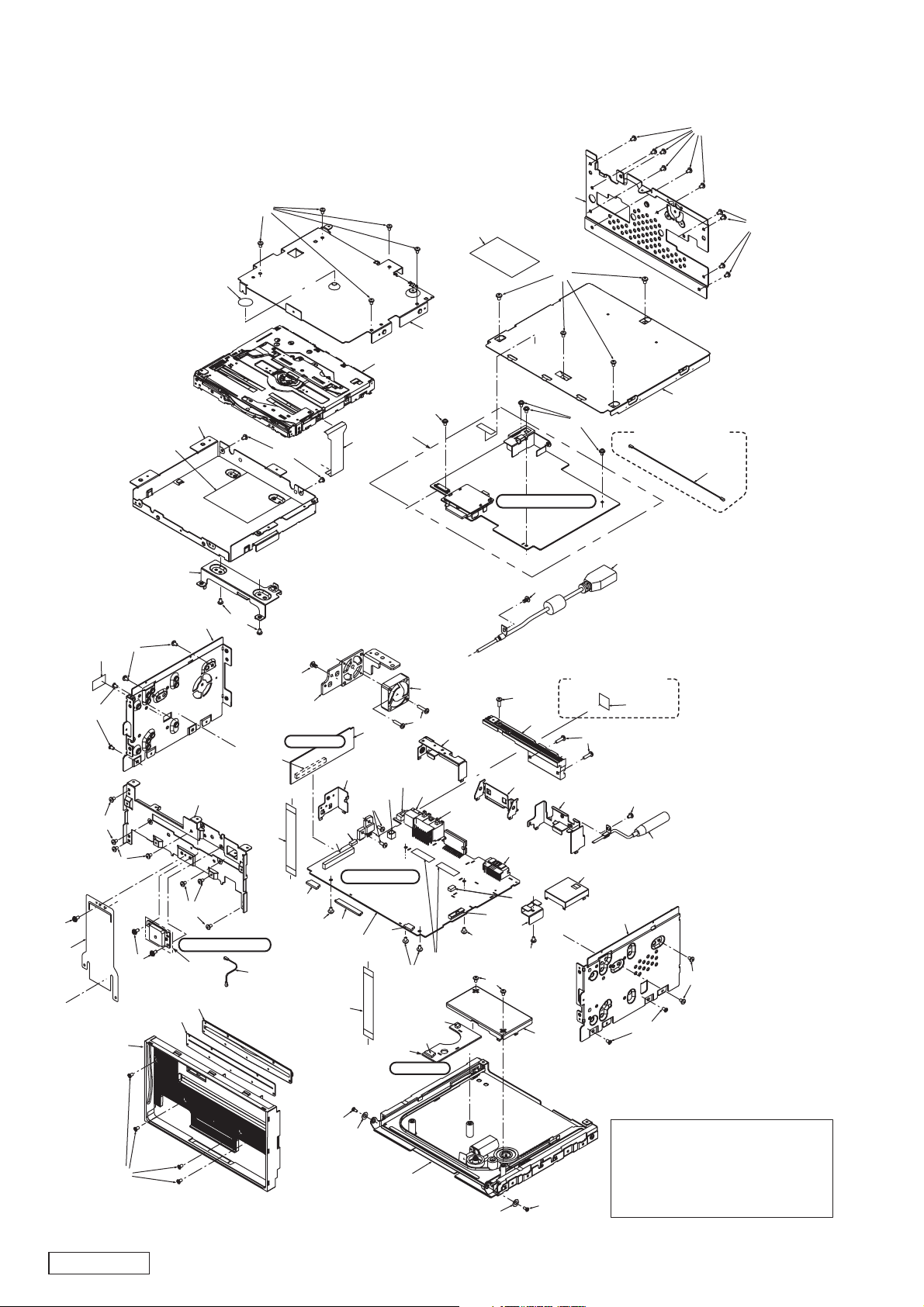
Main section
61
46
35
61
61
62
31
(To Panel PWB)
52
61
MAIN
62
39
47
44
37
36
61
ANT PWB ASSY
29
54
53
56
61
8
61
48
61
22
9
MAIN
MAIN
45
D/D PWB
NV
5
62
15
20
7
3
33
28
34
MAIN
10
14
22
Main PWB
2
1
MAIN
SLIDE
40
62
32
49
57
24
11
13
62
26
25
Slide PWB
27
MAIN
18
12
51
4
62
61
42
61
62
NAVI PWB ASSY
61
< Only NX700E >
60
59
17
19
16
6
55
61
43
61
41
< Only NX700E >
66
30
65
60
22
21
23
38
61
35
64
NX700/NX700E
63
58
50
- 28 -
58
63
No.28 --- When you exchange the parts in
DVD mechanism(929-2170-80),
it is necessary to do inspection and
adjustment by special equipment.
Do not exchange the parts in
DVD mechanism if there is no
special device.
Page 29

Note) Some parts depend on each model. The model name is specified in the description.
1 ----------- MAIN PWB 1
2 074-2233-08 OUTLET SOCKET(MA-SENS 8P) 1
3 074-2233-50 OUTLET SOCKET(MA-PAN 50P) 1
4 074-2238-36 OUTLET SOCKET(MEC-MA 36P) 1
5 074-2233-24 OUTLET SOCKET(MA-NV 24P) 1
6 076-0478-55 PLUG(USB 5P) 1
7 076-0478-57 PLUG(7P) 1
8 092-2239-01 ANT-RECEPT 1
9 074-0881-20 OUTLET SOCKET(20P) 1
10 ----------- D/D PWB 1
11 074-1194-00 OUTLET SOCKET(13P) 1
12 074-4030-00 OUTLET SOCKET(POWER 18P) 1
13 347-7739-20 DOUBLE FACE 2
14 076-0349-02 PLUG(FAN 2P) 1
15 076-0353-20 PLUG(D/D PWB 20P) 1
16 076-0714-24 PLUG(RCA 24P) 1
17 331-4179-00 IC HOLDER(POWER) 1
18 331-4792-00 CONNECT HOLD(L) 1
19 331-4864-00 CONNECT HOLD(R) 1
20 331-4791-00 IC HOLDER(TR) 1
21 092-2216-50 ANT-RECEPT 1
22 714-2606-8B MACHINE SCREW(M2.6x6) 4
23 331-4794-00 TUNER BRKT 1
24 075-0339-00 JACK 1
25 ----------- SLIDE PWB 1
26 074-2225-58 OUTLET SOCKET(8P) 1
27 076-0478-52 PLUG(2P) 1
28 929-2170-80 DVD-MECH-MODULE 1
29 ----------- ANT PWB ASSY 1
30 855-0707-50 USB CABLE 1
31 039-3448-00 FPC(MAIN-PANEL) 1
32 ----------- NAVI PWB ASSY 1
33 816-3040-55 FLAT WIRE(MAIN-SLIDE) 1
34 039-3447-00 FPC(MAIN-MECH) 1
NO. PART NO. DESCRIPTION Q'TYNO. PART NO. DESCRIPTION Q'TY
35 780-2604-51 SCREW(M2.6x4) 4
36 309-1911-00 FRONT PLATE 1
37 312-0503-00 SIDE CHASSIS(L) 1
38 312-0504-00 SIDE CHASSIS(R) 1
39 312-0505-01 CHASSIS 1
40 312-0506-00 UPPER CHASSIS 1
41 310-1831-02 UPPER CASE 1
42 307-0738-01 REAR PLATE 1
43 331-4806-00 PWB HOLDER(SLIDE-PWB) 1
44 331-4807-00 M-PWB HOLDER(MAIN-PWB) 1
45 313-2075-00 HEAT SINK(FAN) 1
46 347-8527-00 SHADE 1
47 347-8504-00 INSULATOR(MECH FPC) 1
48 816-3041-55 FLAT WIRE(MAIN-NAVI) 1
49 020-3053-00 DC-MOTOR(FAN) 1
50 932-0121-80 SLIDE MECH 1
51 276-0720-00 SETPLATE : NX700 1
52 370-6444-02 ESCUTCHEON : NX700 1
53 346-0221-00 LEAHER SHEET 1
54 335-8199-00 DISC GUIDE 1
55 331-4870-00 EARTH PLATE 1
56 347-8760-00 SPACER 1
57 780-2612-50 SCREW(M2.6x12 LOCK) 2
58 335-7903-00 BUSH 2
59 313-2076-00 HEAT SINK(IC) 1
60 714-2608-8H MACHINE SCREW(M2.6x8) 3
61 714-2604-8B MACHINE SCREW(M2.6x4) 38
62 780-2604-50 IT SCREW(M2.6x4) 11
63 716-3577-00 DECORATIVE SCREW 2
64 780-2604-52 SCREW(M2.6x4) 4
65 347-8719-00 SPACER : ONLY NX700E 1
66 092-2204-03 ANT-RECEPT : ONLY NX700E 1
276-0721-00 SETPLATE : NX700E 1
370-6444-03 ESCUTCHEON : NX700E 1
- 29 -
NX700/NX700E
Page 30

ELECTRICAL PARTS LIST
Panel PWB(B1) section
REF No. PART No. DESCRIPTION REF No. PART No. DESCRIPTION REF No. PART No. DESCRIPTION
C104 168-1052-78 16V 1uF K
C108 168-1042-78 16V 0.1uF K
C109 043-0552-90 6.3V 47uF M
C111 168-1042-78 16V 0.1uF K
C112 166-2001-50 20pF CH
C115 166-2001-50 20pF CH
C116 168-1042-78 16V 0.1uF K
C117 166-2001-50 20pF CH
C118 043-0540-00 6.3V 10uF
C119 168-1042-38 50V 0.1uF K
C120 166-4711-50 470pF CH
C121 166-1011-50 100pF CH
C122 043-0566-90 50V 2.2uF K
C124 168-2242-58 0.22uF K
C125 168-1042-78 16V 0.1uF K
C126 166-1011-50 100pF CH
C127 043-0540-00 6.3V 10uF
C128 168-1042-78 16V 0.1uF K
C129 168-1042-78 16V 0.1uF K
C130 168-1042-78 16V 0.1uF K
C131 168-1042-78 16V 0.1uF K
C132 043-0540-00 6.3V 10uF
C134 043-0568-90 25V 2.2uF
C135 043-0568-90 25V 2.2uF
C136 043-0540-00 6.3V 10uF
C137 168-1042-78 16V 0.1uF K
C138 168-1042-78 16V 0.1uF K
C139 166-1021-50 1000pF CH
C140 168-1042-78 16V 0.1uF K
C141 168-1042-78 16V 0.1uF K
C142 043-0540-00 6.3V 10uF
C143 168-1042-78 16V 0.1uF K
C144 168-1042-78 16V 0.1uF K
C145 168-1042-78 16V 0.1uF K
C147 168-1042-78 16V 0.1uF K
C148 166-1801-50 18pF CH
C149 166-1801-50 18pF CH
C150 168-1042-78 16V 0.1uF K
C151 168-1042-78 16V 0.1uF K
C152 168-1042-78 16V 0.1uF K
C153 168-1042-78 16V 0.1uF K
C156 168-1032-55 0.01uF K
C157 168-1042-78 16V 0.1uF K
C158 043-0540-00 6.3V 10uF
C159 168-1042-78 16V 0.1uF K
C160 168-1042-78 16V 0.1uF K
C161 168-1042-78 16V 0.1uF K
C162 168-1042-78 16V 0.1uF K
C164 168-1042-78 16V 0.1uF K
C165 168-1042-78 16V 0.1uF K
C166 168-1042-78 16V 0.1uF K
C167 168-1042-78 16V 0.1uF K
C168 043-6401-90 16V 10uF
C169 168-1042-78 16V 0.1uF K
C170 168-1042-78 16V 0.1uF K
C171 168-1042-78 16V 0.1uF K
C172 168-1042-78 16V 0.1uF K
C173 168-1042-78 16V 0.1uF K
C174 043-0540-00 6.3V 10uF
C175 168-1042-78 16V 0.1uF K
C176 043-6401-90 16V 10uF
C177 168-1042-78 16V 0.1uF K
C178 168-1042-78 16V 0.1uF K
C179 166-2701-50 27pF CH
C180 043-6401-90 16V 10uF
C181 166-4711-50 470pF CH
C182 166-4711-50 470pF CH
C183 166-4711-50 470pF CH
C186 168-1042-78 16V 0.1uF K
C187 168-1032-55 0.01uF K
C188 043-0540-00 6.3V 10uF
Note) Some parts depend on each model. The model name is specified in the description.
C189 043-6401-90 16V 10uF
C190 043-0540-00 6.3V 10uF
C191 166-1521-50 1500pF CH
C192 043-6401-90 16V 10uF
C193 168-1042-78 16V 0.1uF K
C194 168-1032-55 0.01uF K
C195 166-1521-50 1500pF CH
C196 166-1521-50 1500pF CH
C197 043-6401-90 16V 10uF
C198 166-1521-50 1500pF CH
C199 043-0540-00 6.3V 10uF
C200 168-1042-78 16V 0.1uF K
C201 043-0540-00 6.3V 10uF
C202 043-0540-00 6.3V 10uF
C203 043-0566-90 50V 2.2uF K
C204 043-0568-90 25V 2.2uF
C205 168-1042-78 16V 0.1uF K
C206 166-2211-50 220pF CH
C207 043-6401-90 16V 10uF
C208 168-1042-78 16V 0.1uF K
C209 168-1042-78 16V 0.1uF K
C210 168-1042-78 16V 0.1uF K
C211 043-6401-90 16V 10uF
C212 043-6401-90 16V 10uF
C213 166-1021-50 1000pF CH
C214 166-1021-50 1000pF CH
C215 168-1032-55 0.01uF K
C216 168-1032-55 0.01uF K
C217 168-1032-55 0.01uF K
C218 168-1032-55 0.01uF K
C219 168-1032-55 0.01uF K
C257 043-6401-90 16V 10uF
C262 043-0559-90 6.3V 22uF
C701 178-2255-79 2.2uF
C702 043-0549-50 3KV 10PF
C703 043-6401-90 16V 10uF
C704 168-1045-56 25V 0.1uF Z
C705 168-1032-55 0.01uF K
C706 166-3911-50 390pF CH
C707 168-1022-55 1000pF K
C708 168-1032-55 0.01uF K
C709 166-1811-50 180pF CH
C710 168-4722-55 4700pF K
C711 168-6832-78 0.068uF K
C712 178-2255-79 2.2uF
C713 168-2232-55 0.022uF K
C714 043-0567-90 25V 22uF
C715 043-0567-90 25V 22uF
C716 168-1032-55 0.01uF K
C717 043-0567-90 25V 22uF
C720 042-1763-90 25V 47uF M
C721 168-1042-78 16V 0.1uF K
C724 166-1021-50 1000pF CH
C725 043-0554-90 25V 10uF
C726 043-0554-90 25V 10uF
C727 043-0554-90 25V 10uF
C848 043-6401-90 16V 10uF
C901 168-1042-78 16V 0.1uF K
CCT102 050-0140-59 1/32W 33 ohm x4J
CCT104 050-0140-59 1/32W 33 ohm x4J
CCT105 050-0140-59 1/32W 33 ohm x4J
CCT106 050-0140-59 1/32W 33 ohm x4J
CCT107 050-0140-59 1/32W 33 ohm x4J
D100 001-0367-91 1SS226
D101 001-4305-28 UDZSTE-17 12B
D102 001-2643-90 CUS02
D103 001-0367-91 1SS226
D104 001-0367-91 1SS226
D105 001-0367-91 1SS226
D106 001-0367-91 1SS226
D107 001-4305-25 UDZSTE-17 9.1B
D108 001-2643-90 CUS02
D109 001-2643-90 CUS02
D112 001-4305-20 UDZSTE-17 5.6B
D113 001-4305-20 UDZSTE-17 5.6B
D114 001-4305-20 UDZSTE-17 5.6B
D115 001-4305-20 UDZSTE-17 5.6B
D116 001-1306-90 HSU83 TRF-E
D701 001-0529-29 MA8051-M
D703 001-0367-91 1SS226
D704 001-0367-91 1SS226
D901 001-0516-90 MA111
D902 001-7103-90 CL-191HR-CD-T
D903 001-7131-90 SML312WBCW1
WHT
D904 001-7131-90 SML312WBCW1
WHT
D905 001-7131-90 SML312WBCW1
WHT
D909 001-4305-20 UDZSTE-17 5.6B
D910 001-4305-20 UDZSTE-17 5.6B
D911 001-4305-20 UDZSTE-17 5.6B
D912 001-4305-20 UDZSTE-17 5.6B
F701 060-8100-50 1A 1.6X0.8
IC103 051-6467-00 MST7701-I-LF
IC104 052-7094-10 MX25L1605DMI-12G
IC105 051-1292-90 NJM4565M-D
IC701 125-9023-90 TPCF8402TE85L,F
IC702 051-3925-90 OZ9910ISN-T2
IC703 125-9023-90 TPCF8402TE85L,F
IR901 060-4023-90 RS-471
J102 074-2219-54 4P
J103 074-2233-50 50P
J104 074-2226-80 30P
J105 074-2225-66 16P
J901 074-2236-65 15P
L102 010-3104-50 30 ohm/100MHz
L103 010-3105-70 240ohm/100MHz
L104 010-3105-70 240ohm/100MHz
L105 010-3105-70 240ohm/100MHz
L106 010-3105-70 240ohm/100MHz
L107 010-3105-62 1k ohm/100MHz
L108 010-3414-91 3.3uH
L109 010-3514-90 15uH M
L110 010-3514-90 15uH M
L111 010-3104-50 30 ohm/100MHz
L112 010-3506-90 47uH
L113 010-3506-90 47uH
L114 010-3104-50 30 ohm/100MHz
L115 010-3103-70 MMZ1608Y121BTA00
L116 010-3104-50 30 ohm/100MHz
L117 010-3104-50 30 ohm/100MHz
L118 010-3104-50 30 ohm/100MHz
L119 010-3104-50 30 ohm/100MHz
L120 010-3104-50 30 ohm/100MHz
L121 010-3407-68 33uH J
L122 010-3104-50 30 ohm/100MHz
L123 010-3104-50 30 ohm/100MHz
L124 010-3104-50 30 ohm/100MHz
L125 010-3104-50 30 ohm/100MHz
L126 010-3407-62 10uH J
L127 010-3506-90 47uH
L128 010-3505-90 22uH
L129 010-3104-50 30 ohm/100MHz
L130 010-3104-50 30 ohm/100MHz
L131 010-3105-62 1k ohm/100MHz
L132 010-3105-62 1k ohm/100MHz
L133 010-3105-62 1k ohm/100MHz
L134 010-3105-62 1k ohm/100MHz
L135 010-3105-62 1k ohm/100MHz
L136 010-3105-62 1k ohm/100MHz
L137 010-3105-62 1k ohm/100MHz
NX700/NX700E
- 30 -
Page 31

REF No. PART No. DESCRIPTION REF No. PART No. DESCRIPTION REF No. PART No. DESCRIPTION
L138 010-3105-62 1k ohm/100MHz
L139 010-3105-62 1k ohm/100MHz
L140 010-3105-62 1k ohm/100MHz
L141 010-3105-69 80 ohm/100MHz
L142 010-3105-69 80 ohm/100MHz
L143 010-3105-69 80 ohm/100MHz
L701 010-3059-90 200 ohm FILTER
L702 010-3108-54 600 ohm/100MHz
L703 010-3108-54 600 ohm/100MHz
P701 076-0529-02 2P
Q100 125-7011-90 RSR025P03TL
Q102 125-7011-90 RSR025P03TL
Q103 125-7011-90 RSR025P03TL
Q104 125-3014-90 ISA1602AM1 E,F
Q105 125-3014-90 ISA1602AM1 E,F
Q106 125-8028-90 RSR025N03 TL
Q107 125-7011-90 RSR025P03TL
Q108 125-0034-93 RT1P241M
Q109 125-2041-93 RT1N241M
Q110 125-2041-93 RT1N241M
Q112 125-2041-93 RT1N241M
Q113 125-0034-93 RT1P241M
Q701 125-0025-92 RN2302
Q702 125-2032-92 RN1302
Q705 192-4155-49 2SC4155A R,S
Q901 192-4081-00 2SC4081
Q902 192-4081-00 2SC4081
R101 119-1301-15 1/10W 13 ohm
R102 032-0217-56 1/3W 0.047 ohm
R103 119-1031-15 1/10W 10k ohm
R105 032-0140-12 1/10W 75 ohm F
R106 119-1301-15 1/10W 13 ohm
R108 119-6201-15 1/10W 62 ohm
R109 119-1301-15 1/10W 13 ohm
R110 032-0217-56 1/3W 0.047 ohm
R111 032-0140-12 1/10W 75 ohm F
R114 119-6201-15 1/10W 62 ohm
R115 119-1301-15 1/10W 13 ohm
R116 032-0140-12 1/10W 75 ohm F
R117 119-6201-15 1/10W 62 ohm
R118 119-6201-15 1/10W 62 ohm
R119 032-0219-50 1/8W 0.22 ohm
R120 119-6201-15 1/10W 62 ohm
R121 032-0140-12 1/10W 75 ohm F
R123 119-6201-15 1/10W 62 ohm
R124 032-0140-04 1/10W 8.2k ohm F
R125 032-0140-50 1/10W 10k ohm F
R126 032-0140-99 1/10W 39k ohm F
R127 032-0140-55 1/10W 4.7k ohm F
R128 119-0000-05 1/10W 0 ohm JW
R131 119-3311-15 1/10W 330 ohm
R132 119-1021-15 1/10W 1k ohm
R133 119-4791-15 1/10W 4.7 ohm
R136 119-4721-15 1/10W 4.7k ohm
R137 119-3301-15 1/10W 33 ohm
R139 119-1041-15 1/10W 100k ohm
R140 119-1051-15 1/10W 1M ohm
R141 119-1001-15 1/10W 10 ohm
R144 119-0000-05 1/10W 0 ohm JW
R145 119-1031-15 1/10W 10k ohm
R146 119-2221-15 1/10W 2.2k ohm
R147 119-2221-15 1/10W 2.2k ohm
R149 119-3331-15 1/10W 33k ohm
R150 119-3331-15 1/10W 33k ohm
R151 119-1031-15 1/10W 10k ohm
R152 119-1031-15 1/10W 10k ohm
R153 119-3331-15 1/10W 33k ohm
R154 119-3321-15 1/10W 3.3k ohm
R155 119-3331-15 1/10W 33k ohm
R157 032-0140-04 1/10W 8.2k ohm F
R158 119-1031-15 1/10W 10k ohm
R159 119-2231-15 1/10W 22k ohm
R160 032-0140-52 1/10W 33k ohm F
R161 119-1031-15 1/10W 10k ohm
R163 032-0217-56 1/3W 0.047 ohm
R165 119-0000-05 1/10W 0 ohm JW
R166 119-0000-05 1/10W 0 ohm JW
R168 032-0219-50 1/8W 0.22 ohm
R169 032-0140-94 1/10W 30k ohm F
R170 119-0000-05 1/10W 0 ohm JW
R171 119-0000-05 1/10W 0 ohm JW
R172 119-0000-05 1/10W 0 ohm JW
R173 032-0140-08 1/10W 13k ohm F
R177 032-0140-50 1/10W 10k ohm F
R178 119-3301-15 1/10W 33 ohm
R179 119-3301-15 1/10W 33 ohm
R180 119-3301-15 1/10W 33 ohm
R181 119-1211-15 1/10W 120 ohm
R182 119-0000-05 1/10W 0 ohm JW
R183 119-0000-05 1/10W 0 ohm JW
R185 119-0000-05 1/10W 0 ohm JW
R188 119-0000-05 1/10W 0 ohm JW
R194 116-5611-15 1/4W 560 ohm
R197 119-4731-15 1/10W 47k ohm
R198 119-4731-15 1/10W 47k ohm
R199 119-0000-05 1/10W 0 ohm JW
R200 119-0000-05 1/10W 0 ohm JW
R201 119-4731-15 1/10W 47k ohm
R202 119-0000-05 1/10W 0 ohm JW
R203 119-6891-15 1/10W 6.8 ohm
R204 119-6891-15 1/10W 6.8 ohm
R205 119-6891-15 1/10W 6.8 ohm
R206 119-6891-15 1/10W 6.8 ohm
R208 119-0000-05 1/10W 0 ohm JW
R213 119-0000-05 1/10W 0 ohm JW
R215 119-4721-15 1/10W 4.7k ohm
R216 119-4731-15 1/10W 47k ohm
R217 119-4721-15 1/10W 4.7k ohm
R218 119-4731-15 1/10W 47k ohm
R221 119-0000-05 1/10W 0 ohm JW
R250 119-4731-15 1/10W 47k ohm
R252 119-2211-15 1/10W 220 ohm
R253 119-1511-15 1/10W 150 ohm
R254 119-1511-15 1/10W 150 ohm
R255 119-1511-15 1/10W 150 ohm
R260 119-1041-15 1/10W 100k ohm
R261 119-1041-15 1/10W 100k ohm
R262 119-4731-15 1/10W 47k ohm
R263 119-4731-15 1/10W 47k ohm
R264 119-4731-15 1/10W 47k ohm
R701 116-6811-15 1/4W 680 ohm
R702 119-1041-15 1/10W 100k ohm
R703 119-3931-15 1/10W 39k ohm
R705 032-0140-05 1/10W 82k ohm F
R706 119-3351-15 1/10W 3.3M ohm
R707 119-1021-15 1/10W 1k ohm
R708 119-1021-15 1/10W 1k ohm
R709 119-1031-15 1/10W 10k ohm
R711 119-6841-15 1/10W 680k ohm
R712 119-1051-15 1/10W 1M ohm
R713 032-0140-79 1/10W 2.7k ohm F
R714 032-0140-90 1/10W 560 ohm F
R715 119-1021-15 1/10W 1k ohm
R716 119-1021-15 1/10W 1k ohm
R720 119-1021-15 1/10W 1k ohm
R721 119-1021-15 1/10W 1k ohm
R901 119-1021-15 1/10W 1k ohm
R902 119-1011-15 1/10W 100 ohm
R903 119-3311-15 1/10W 330 ohm
R904 119-3311-15 1/10W 330 ohm
R905 119-3311-15 1/10W 330 ohm
R906 119-2211-15 1/10W 220 ohm
R907 119-5611-15 1/10W 560 ohm
S901 013-6312-50 SKRP-ABE-010
S902 013-6318-51 SKRKAEE010
S903 013-6318-51 SKRKAEE010
S904 013-6318-51 SKRKAEE010
T701 007-1178-00 OUTPUT-TRANS
BLC4126
TM100 073-0762-90 TERMINAL
TM101 073-0762-90 TERMINAL
TM102 073-0762-90 TERMINAL
TM103 073-0762-90 TERMINAL
TM104 073-0785-90 TERMINAL
TM105 073-0785-90 TERMINAL
X101 061-3569-90 NX3225GA
PWB 039-3500-00 PWB(WITHOUT
COMPONENTS)
- 31 -
NX700/NX700E
Page 32

Main PWB(B2) section
REF No. PART No. DESCRIPTION REF No. PART No. DESCRIPTION REF No. PART No. DESCRIPTION
ANT201 092-2216-50 ANTENNA RECEPT
ANT202 092-2203-00 ANT-RECEPT
(NX700E)
C101 168-1022-55 1000pF K
C102 166-2096-50 2pF +/-0.25pF CK
C104 166-1501-50 15pF CH
C105 168-1022-55 1000pF K
C106 166-3901-50 39pF CH
C107 168-2242-58 0.22uF K
C108 166-1201-50 12pF CH
C109 168-2242-58 0.22uF K
C110 168-1052-78 16V 1uF K
C111 168-2242-58 0.22uF K
C112 166-1201-50 12pF CH
C113 168-1052-78 16V 1uF K
C114 168-1032-55 0.01uF K
C115 168-1032-55 0.01uF K
C116 168-1032-55 0.01uF K
C117 168-1042-78 16V 0.1uF K
C118 168-1042-78 16V 0.1uF K
C119 168-1032-55 0.01uF K
C120 168-2232-55 0.022uF K
C121 177-1062-78 10pF
C122 168-1042-78 16V 0.1uF K
C123 168-1042-78 16V 0.1uF K
C124 043-6401-90 16V 10uF
(NX700E)
C200 166-2201-50 22pF CH
C202 168-1042-78 16V 0.1uF K
C203 043-0540-00 6.3V 10uF
C204 043-0540-00 6.3V 10uF
C205 166-2211-50 220pF CH
C206 166-2211-50 220pF CH
C207 043-0540-00 6.3V 10uF
C208 043-0540-00 6.3V 10uF
C209 043-0540-00 6.3V 10uF
C210 043-0540-00 6.3V 10uF
C211 168-1042-78 16V 0.1uF K
C213 168-1052-78 16V 1uF K
(NX700)
C214 168-1052-78 16V 1uF K
(NX700)
C215 168-1052-78 16V 1uF K
(NX700)
C216 168-1052-78 16V 1uF K
(NX700)
C217 168-1052-78 16V 1uF K
C218 043-0540-00 6.3V 10uF
C219 168-1052-78 16V 1uF K
C220 168-1052-78 16V 1uF K
C221 168-1052-78 16V 1uF K
C227 166-1211-50 120pF CH
C228 166-1211-50 120pF CH
C229 166-5611-50 560pF CH
C230 166-5611-50 560pF CH
C231 166-5611-50 560pF CH
C232 166-5611-50 560pF CH
C233 166-5611-50 560pF CH
C234 166-2201-50 22pF CH
C235 166-5611-50 560pF CH
C236 166-2201-50 22pF CH
C237 166-5611-50 560pF CH
C238 166-5611-50 560pF CH
C243 168-1042-78 16V 0.1uF K
C245 042-1764-90 16V 100uF M
C246 168-1042-78 16V 0.1uF K
C247 166-2096-50 2pF +/-0.25pF CK
(NX700)
C248 166-3901-50 39pF CH
(NX700E)
C249 166-2096-50 2pF+/-0.25pF CK
(NX700E)
C250 166-3901-50 39pF CH
(NX700E)
C251 168-1052-78 16V 1uF K
C252 168-1052-78 16V 1uF K
C253 165-4763-35 16V 47uF
(NX700E)
C256 168-1042-78 16V 0.1uF K
C257 168-1042-78 16V 0.1uF K
C258 165-4763-35 16V 47uF
C259 168-1042-78 16V 0.1uF K
(NX700E)
C260 168-1042-78 16V 0.1uF K
C261 166-5611-50 560pF CH
(NX700E)
C262 168-1042-78 16V 0.1uF K
C263 165-4763-35 16V 47uF
C264 166-3311-50 330pF CH
(NX700E)
C265 166-2201-50 22pF CH
(NX700E)
C268 165-1063-35 16V 10uF
(NX700E)
C269 166-3301-50 33pF CH
(NX700E)
C271 166-2201-50 22pF CH
(NX700E)
C272 168-1022-55 1000pF K
C273 168-1022-55 1000pF K
C274 168-1022-55 1000pF K
C275 168-1042-78 16V 0.1uF K
C279 166-2201-50 22pF CH
C280 166-2201-50 22pF CH
C282 168-1042-78 16V 0.1uF K
C283 168-1042-78 16V 0.1uF K
C284 168-1042-78 16V 0.1uF K
C285 168-1042-78 16V 0.1uF K
C287 168-1052-78 16V 1uF K
C288 165-1063-35 16V 10uF
C292 168-1042-78 16V 0.1uF K
(NX700E)
C293 168-1042-78 16V 0.1uF K
C294 165-1063-35 16V 10uF
C295 165-1063-35 16V 10uF
C296 165-1063-35 16V 10uF
C297 165-1063-35 16V 10uF
C298 165-1063-35 16V 10uF
C299 165-1063-35 16V 10uF
C300 165-1063-35 16V 10uF
C301 165-1063-35 16V 10uF
C302 166-3911-50 390pF CH
C303 166-3911-50 390pF CH
C304 043-0540-00 6.3V 10uF
C305 043-0540-00 6.3V 10uF
C322 168-1022-55 1000pF K
C323 168-1022-55 1000pF K
C324 168-2242-58 0.22uF K
C325 168-2242-58 0.22uF K
C326 168-2242-58 0.22uF K
C327 168-2242-58 0.22uF K
C385 166-1011-50 100pF CH
C386 166-1011-50 100pF CH
C387 168-1042-78 16V 0.1uF K
C388 168-1032-55 0.01uF K
C401 043-0540-00 6.3V 10uF
C404 043-0540-00 6.3V 10uF
C405 043-0540-00 6.3V 10uF
C406 168-1042-78 16V 0.1uF K
C407 043-6401-90 16V 10uF
C408 166-1007-50 10pF CH
C410 168-1022-55 1000pF K
C423 168-1042-78 16V 0.1uF K
C424 168-1042-78 16V 0.1uF K
C425 168-1042-78 16V 0.1uF K
C426 168-1042-78 16V 0.1uF K
C427 042-1764-90 16V 100uF M
C428 168-1042-78 16V 0.1uF K
C429 168-1052-78 16V 1uF K
C430 168-1052-78 16V 1uF K
C431 168-1042-78 16V 0.1uF K
C432 168-1052-78 16V 1uF K
C433 168-1052-78 16V 1uF K
C435 168-1052-78 16V 1uF K
C436 168-1022-55 1000pF K
C455 042-1764-90 16V 100uF M
C456 043-6401-90 16V 10uF
(NX700E)
C457 043-6401-90 16V 10uF
(NX700E)
C460 168-1032-55 0.01uF K
C491 043-0551-90 6.3V 4.7uF M
C492 043-0551-90 6.3V 4.7uF M
C501 043-0540-00 6.3V 10uF
C504 168-1042-78 16V 0.1uF K
C505 168-1042-78 16V 0.1uF K
C506 043-0540-00 6.3V 10uF
C507 168-1042-78 16V 0.1uF K
C508 043-0551-90 6.3V 4.7uF M
C509 166-2201-50 22pF CH
C510 168-1032-55 0.01uF K
C511 168-1022-55 1000pF K
C512 168-1052-78 16V 1uF K
C513 168-1042-78 16V 0.1uF K
C514 168-4732-78 0.047uF K
C515 165-1063-35 16V 10uF
C516 042-4022-90 6.3V 1000uF
C517 168-1052-78 16V 1uF K
C518 165-4763-15 6.3V 47uF
C520 168-1042-78 16V 0.1uF K
C521 166-1201-50 12pF CH
C522 166-1201-50 12pF CH
C523 166-1011-50 100pF CH
C527 168-1022-55 1000pF K
C528 042-1764-90 16V 100uF M
C530 168-1042-78 16V 0.1uF K
C531 165-2263-35 16V 22uF
C532 168-1042-78 16V 0.1uF K
C534 043-6401-90 16V 10uF
C535 043-6401-90 16V 10uF
C601 168-2222-55 2200pF K
C602 168-2222-55 2200pF K
C603 168-2222-55 2200pF K
C604 168-2222-55 2200pF K
C605 168-2222-55 2200pF K
C606 168-2222-55 2200pF K
C607 168-2222-55 2200pF K
C608 168-2222-55 2200pF K
C610 165-4763-35 16V 47uF
C611 168-1052-78 16V 1uF K
C612 165-1053-65 50V 1uF
C613 042-1545-00 16V 2200uF
C616 172-2241-11 0.22uF
C617 042-1545-00 16V 2200uF
C619 042-1764-90 16V 100uF M
C620 168-1042-78 16V 0.1uF K
C622 168-1042-78 16V 0.1uF K
C623 168-1032-55 0.01uF K
C625 165-4763-35 16V 47uF
C626 168-1042-78 16V 0.1uF K
C630 165-3363-45 25V 33uF
C633 042-1764-90 16V 100uF M
C634 043-6401-90 16V 10uF
C635 043-6401-90 16V 10uF
C636 168-4732-78 0.047uF K
C637 043-6401-90 16V 10uF
C638 043-0540-00 6.3V 10uF
C639 043-0540-00 6.3V 10uF
NX700/NX700E
- 32 -
Page 33

REF No. PART No. DESCRIPTION REF No. PART No. DESCRIPTION REF No. PART No. DESCRIPTION
C640 168-1052-78 16V 1uF K
C641 166-1011-50 100pF CH
C642 043-6401-90 16V 10uF
C643 043-6401-90 16V 10uF
C671 168-3342-58 0.33uF K
C701 043-0540-00 6.3V 10uF
C702 043-0540-00 6.3V 10uF
C703 042-4022-90 6.3V 1000uF
C704 046-1042-78 0.1uF K B
C705 043-0559-90 6.3V 22uF
C706 168-1042-78 16V 0.1uF K
C707 168-1042-78 16V 0.1uF K
C708 043-0540-00 6.3V 10uF
C709 168-1042-78 16V 0.1uF K
C710 043-0540-00 6.3V 10uF
C711 046-1042-78 0.1uF K B
C712 046-1042-78 0.1uF K B
C713 045-1007-50 10 +/-0.5pF CH
C714 045-1007-50 10 +/-0.5pF CH
C715 168-1042-78 16V 0.1uF K
C716 046-1042-78 0.1uF K B
C717 046-2222-58 2200pF K B
C718 046-1042-78 0.1uF K B
C719 168-1042-78 16V 0.1uF K
C720 046-1032-78 0.01uF K B
C721 046-1042-78 0.1uF K B
C722 046-1042-78 0.1uF K B
C723 043-0552-90 6.3V 47uF M
C725 046-1042-78 0.1uF K B
C726 046-1042-78 0.1uF K B
C727 046-1042-78 0.1uF K B
C728 046-1042-78 0.1uF K B
C730 045-1801-50 18pFJ CH
C731 045-1801-50 18pFJ CH
C732 046-1042-78 0.1uF K B
C733 046-1032-78 0.01uF K B
C734 045-1007-50 10 +/-0.5pF CH
C735 045-1007-50 10 +/-0.5pF CH
C736 168-1042-78 16V 0.1uF K
C737 046-1042-78 0.1uF K B
C738 046-1032-78 0.01uF K B
C739 168-1042-78 16V 0.1uF K
C740 168-1042-78 16V 0.1uF K
C741 043-0540-00 6.3V 10uF
C742 043-0540-00 6.3V 10uF
C743 166-2211-50 220pF CH
C744 166-2211-50 220pF CH
C745 168-1042-78 16V 0.1uF K
C746 043-0552-90 6.3V 47uF M
C747 043-0552-90 6.3V 47uF M
C749 043-0540-00 6.3V 10uF
C750 168-1042-78 16V 0.1uF K
C751 168-1042-78 16V 0.1uF K
C752 043-0552-90 6.3V 47uF M
C755 168-1022-55 1000pF K
C756 168-1022-55 1000pF K
C757 168-1032-55 0.01uF K
C758 168-1022-55 1000pF K
C759 168-1042-78 16V 0.1uF K
C760 043-6401-90 16V 10uF
(NX700E)
C761 043-6401-90 16V 10uF
(NX700E)
CCT708 050-0140-63 1/32W 47k ohm x4J
D351 001-0529-14 MA8030-L
D352 001-0529-14 MA8030-L
D353 001-0529-14 MA8030-L
D354 001-0529-14 MA8030-L
D355 001-0529-14 MA8030-L
D356 001-0529-14 MA8030-L
D361 001-0516-90 MA111
D362 001-0516-90 MA111
D363 001-0529-44 MA8082-M
D389 001-0516-90 MA111
D390 001-0516-90 MA111
D391 001-0516-90 MA111
D421 001-0529-14 MA8030-L
D422 001-0529-14 MA8030-L
D504 001-0529-53 MA8110M
D515 001-0516-90 MA111
D516 001-4313-50 HZU6A2L
D602 001-0516-90 MA111
D603 001-0516-90 MA111
D604 001-4912-90 SM5S22A-HE3/2D
D606 001-0516-90 MA111
D607 001-0529-14 MA8030-L
D608 001-0516-90 MA111
D609 001-0516-90 MA111
D610 001-0516-90 MA111
D611 001-2403-90 M1F60
D613 001-2403-90 M1F60
D614 001-0516-90 MA111
D615 001-0529-26 MA8047-M
D616 001-2403-90 M1F60
D617 001-2403-90 M1F60
D618 001-0516-90 MA111
D619 001-2403-90 M1F60
D620 001-0504-47 HZS9 B3L
D623 001-2403-90 M1F60
(NX700)
D624 001-0529-32 MA8056-M
D625 001-0529-69 MA8180-M
D626 001-0529-69 MA8180-M
D703 060-8101-50 TEW2XCP020V
IC101 051-4700-90 TEF6606/V4
IC200 051-6739-90 AK4388ET-E2
IC205 051-3034-90 NJM4558V
IC207 051-3034-90 NJM4558V
IC208 051-7106-90 CD4052B-PWR
IC209 051-5048-90 NJW1222-TE2
IC210 051-4620-90 LC72725KM
(NX700E)
IC212 051-3034-90 NJM4558V
IC381 051-7262-48 TC7WH14FU-
TE12L,F
IC421 051-5352-90 AK4254
IC491 051-3568-90 S-1172B19-E6T1G
IC503 ----------- uPD70F3354GJ-
GAE-A(FLASH
033100-052)
IC504 051-5440-08 S-80931CNMC-G81
IC505 051-3406-90 NJM2078M
IC506 051-5410-38 BU4820G-TR
IC507 051-9432-90 S-24CS04AFT-V-G
IC508 051-6100-90 BD6221F-E2
IC601 051-2070-00 TB2926HQ
IC602 051-3335-90 AN77L04M
IC605 051-6600-90 LA2335M(NX700)
IC701 051-3579-90 S1112B15MCL6ATFG
IC702 051-3579-90 S1112B15MCL6ATFG
IC703 051-6711-40 TC94A34FG-010
IC704 051-6739-90 AK4388ET-E2
IC705 052-3409-30 TMP92FD28AFG
IC706 051-6926-90 BD2051AFJ-TR
IC707 051-5418-08 S-80827CNMC-B8K
IC708 051-7226-08 TC7SH00FU
IC709 051-6934-90 MFI341S2313
J382 074-2233-24 24P
J401 074-2238-36 36P
J452 074-2233-50 50P
J502 074-2233-08 8P
J506 075-0339-00 MINI JACK
J601 074-4030-00 OUTLET SOCKET
J602 074-1194-00 13P Ce-NET(NX700)
L101 010-3406-50 1uH J
L102 010-3406-53 1.8uH J
L103 010-3062-54 290nH
L104 010-3406-43 0.27uH J
L105 010-3072-90 560uH
L106 010-3072-90 560uH
L107 010-4054-00 35.7pF/100MHz
L108 010-3105-62 1k ohm/100MHz
L109 010-3105-62 1k ohm/100MHz
L200 010-2198-87 0.082uH
(NX700E)
L201 010-8037-00 0.545uH M
(NX700E)
L202 010-8037-01 0.85uH M
(NX700E)
L203 010-2198-87 0.082uH
(NX700)
117-0000-05 1/8W 0 ohm JW
(NX700E)
L204 010-2003-04 30uH
L205 010-3407-58 4.7uH J
L206 010-3105-62 1k ohm/100MHz
L207 010-3103-64 1.5k ohm/100MHz
L208 010-3103-64 1.5k ohm/100MHz
L209 010-3407-78 220uH J
(NX700E)
L210 010-3103-64 1.5k ohm/100MHz
L211 010-3103-64 1.5k ohm/100MHz
L212 010-3103-64 1.5k ohm/100MHz
L213 010-3103-64 1.5k ohm/100MHz
L214 010-3103-64 1.5k ohm/100MHz
L215 010-3103-64 1.5k ohm/100MHz
L216 010-3103-64 1.5k ohm/100MHz
L217 010-3103-64 1.5k ohm/100MHz
L218 010-3103-64 1.5k ohm/100MHz
L219 010-3103-64 1.5k ohm/100MHz
L220 010-3104-53 220 ohm/100MHz
L221 010-3105-62 1k ohm/100MHz
(NX700E)
L222 010-3103-64 1.5k ohm/100MHz
L223 010-3103-64 1.5k ohm/100MHz
L401 010-3103-50 1500 ohm/100MHz
L402 010-3103-50 1500 ohm/100MHz
L403 010-3103-50 1500 ohm/100MHz
L404 010-3103-55 120 ohm/100MHz
L405 010-3103-64 1.5k ohm/100MHz
L406 010-3103-64 1.5k ohm/100MHz
L407 010-3103-64 1.5k ohm/100MHz
L408 010-3104-50 30 ohm/100MHz
L409 010-3104-50 30 ohm/100MHz
L411 010-3104-50 30 ohm/100MHz
L412 010-3041-90 10uH
L413 010-3103-64 1.5k ohm/100MHz
L421 010-3406-66 22uH J
L491 010-3104-50 30 ohm/100MHz
L501 010-2279-50 4.7uH
L502 010-2279-50 4.7uH
L503 010-3407-78 220uH J
L551 010-3108-54 600 ohm/100MHz
L552 010-3108-54 600 ohm/100MHz
L601 010-3407-66 22uH J
L602 010-3104-50 30 ohm/100MHz
L603 010-3104-50 30 ohm/100MHz
L701 010-3103-64 1.5k ohm/100MHz
L702 010-3103-64 1.5k ohm/100MHz
L703 010-3103-64 1.5k ohm/100MHz
L704 010-3103-55 120 ohm/100MHz
L705 010-3103-64 1.5k ohm/100MHz
L706 010-3103-64 1.5k ohm/100MHz
L707 010-3105-62 1k ohm/100MHz
L708 010-3104-53 220 ohm/100MHz
P203 076-0714-24 PLUG
P504 076-0478-57 7P
P601 076-0349-02 2P
P602 076-0353-20 20P
- 33 -
NX700/NX700E
Page 34
REF No. PART No. DESCRIPTION REF No. PART No. DESCRIPTION REF No. PART No. DESCRIPTION
P702 076-0478-55 6P
Q201 125-2041-93 RT1N241M
Q202 125-2041-93 RT1N241M
Q203 192-6053-00 2SC6053
Q204 192-6053-00 2SC6053
Q205 192-6053-00 2SC6053
Q206 192-6053-00 2SC6053
Q207 192-6053-00 2SC6053
Q208 192-6053-00 2SC6053
Q209 192-6053-00 2SC6053
Q210 192-6053-00 2SC6053
Q211 192-4155-49 2SC4155A R,S
Q212 192-4155-49 2SC4155A R,S
Q213 192-4155-49 2SC4155A R,S
Q214 192-4155-49 2SC4155A R,S
Q215 125-0034-96 RT1P436M
Q216 125-0034-96 RT1P436M
Q217 125-0034-96 RT1P436M
Q218 125-0034-96 RT1P436M
Q219 125-2041-96 RT1N436M
Q220 192-4155-49 2SC4155A R,S
Q221 125-2041-96 RT1N436M
Q222 192-4155-49 2SC4155A R,S
Q381 192-4155-49 2SC4155A R,S
Q382 192-4155-49 2SC4155A R,S
Q383 125-2041-93 RT1N241M
Q384 125-3014-90 ISA1602AM1 E,F
Q385 125-3014-90 ISA1602AM1 E,F
Q401 190-1365-50 2SA1365 AF,AG
Q402 125-2041-96 RT1N436M
Q403 190-2071-00 2SA2071
Q404 125-2041-96 RT1N436M
Q451 190-2071-00 2SA2071
Q452 192-4155-49 2SC4155A R,S
Q501 192-4155-49 2SC4155A R,S
Q502 192-4155-49 2SC4155A R,S
Q503 192-4155-49 2SC4155A R,S
Q504 125-0034-93 RT1P241M
Q505 125-3014-90 ISA1602AM1 E,F
Q506 192-4155-49 2SC4155A R,S
Q507 125-2041-92 RT1N141M
Q511 125-2041-96 RT1N436M
Q601 125-4021-90 3CG1260 Q
Q604 125-3014-90 ISA1602AM1 E,F
Q605 192-4155-49 2SC4155A R,S
Q607 192-4155-49 2SC4155A R,S
Q610 125-4021-90 3CG1260 Q
Q612 125-4021-90 3CG1260 Q
Q614 125-3014-90 ISA1602AM1 E,F
Q616 125-2041-96 RT1N436M
Q617 125-2041-96 RT1N436M
Q618 192-4155-49 2SC4155A R,S
Q619 192-4155-49 2SC4155A R,S
Q620 102-3420-50 2SC3420 GR,BL
Q621 125-3014-90 ISA1602AM1 E,F
Q623 125-2041-96 RT1N436M
Q627 125-2041-96 RT1N436M
Q628 192-5824-00 2SC5824
Q634 101-1375-00 2SB1375
Q701 190-1365-50 2SA1365 AF,AG
Q703 125-2041-93 RT1N241M
Q706 125-0034-96 RT1P436M
Q707 125-2041-93 RT1N241M
R101 119-4741-15 1/10W 470k ohm
R102 119-4741-15 1/10W 470k ohm
R103 119-1011-15 1/10W 100 ohm
R104 119-4721-15 1/10W 4.7k ohm
R105 116-2201-15 1/4W 22 ohm
R106 119-1011-15 1/10W 100 ohm
R107 119-1011-15 1/10W 100 ohm
R108 119-0000-05 1/10W 0 ohm JW
R115 119-0000-05 1/10W 0 ohm JW
(NX700E)
R116 119-0000-05 1/10W 0 ohm JW
(NX700)
R200 119-1021-15 1/10W 1k ohm
R203 119-4731-15 1/10W 47k ohm
R204 119-4731-15 1/10W 47k ohm
R207 119-1011-15 1/10W 100 ohm
R216 119-0000-05 1/10W 0 ohm JW
(NX700E)
R220 119-0000-05 1/10W 0 ohm JW
(NX700)
R221 119-2731-15 1/10W 27k ohm
R222 119-2731-15 1/10W 27k ohm
R223 119-5621-15 1/10W 5.6k ohm
R224 119-5621-15 1/10W 5.6k ohm
R225 119-1511-15 1/10W 150 ohm
(NX700E)
R226 119-0000-05 1/10W 0 ohm JW
(NX700)
R227 119-0000-05 1/10W 0 ohm JW
(NX700)
R229 119-0000-05 1/10W 0 ohm JW
(NX700)
R230 119-0000-05 1/10W 0 ohm JW
(NX700)
R231 032-0140-89 1/10W 47k ohm F
R232 032-0140-63 1/10W 27k ohm F
R233 032-0140-89 1/10W 47k ohm F
R234 119-1831-15 1/10W 18k ohm
(NX700)
R235 119-5631-15 1/10W 56k ohm
(NX700)
R236 119-5631-15 1/10W 56k ohm
(NX700)
R237 032-0140-89 1/10W 47k ohm F
R238 032-0140-63 1/10W 27k ohm F
R239 032-0140-89 1/10W 47k ohm F
R240 119-1831-15 1/10W 18k ohm
(NX700)
R241 119-1831-15 1/10W 18k ohm
(NX700)
R242 119-5631-15 1/10W 56k ohm
(NX700)
R243 119-5631-15 1/10W 56k ohm
(NX700)
R244 032-0140-63 1/10W 27k ohm F
R245 119-0000-05 1/10W 0 ohm JW
R246 032-0140-63 1/10W 27k ohm F
R247 119-1831-15 1/10W 18k ohm
(NX700)
R255 119-1031-15 1/10W 10k ohm
R260 032-0140-89 1/10W 47k ohm F
R261 032-0140-89 1/10W 47k ohm F
R263 032-0140-55 1/10W 4.7k ohm F
R264 032-0140-55 1/10W 4.7k ohm F
R267 119-1021-15 1/10W 1k ohm
(NX700E)
R268 119-1021-15 1/10W 1k ohm
(NX700E)
R275 119-4731-15 1/10W 47k ohm
R278 119-4731-15 1/10W 47k ohm
R279 119-1011-15 1/10W 100 ohm
R280 119-1011-15 1/10W 100 ohm
R281 119-6831-15 1/10W 68k ohm
R282 119-6831-15 1/10W 68k ohm
R283 119-4731-15 1/10W 47k ohm
R284 119-4731-15 1/10W 47k ohm
R285 119-2231-15 1/10W 22k ohm
R286 119-2231-15 1/10W 22k ohm
R287 119-2231-15 1/10W 22k ohm
R288 119-2231-15 1/10W 22k ohm
R289 119-2231-15 1/10W 22k ohm
R290 119-2231-15 1/10W 22k ohm
R291 119-2231-15 1/10W 22k ohm
R292 119-2231-15 1/10W 22k ohm
R293 119-1031-15 1/10W 10k ohm
R294 119-1031-15 1/10W 10k ohm
R295 119-3311-15 1/10W 330 ohm
R296 119-1021-15 1/10W 1k ohm
R297 119-1021-15 1/10W 1k ohm
R298 119-3311-15 1/10W 330 ohm
R299 119-3311-15 1/10W 330 ohm
R300 119-1021-15 1/10W 1k ohm
R301 119-1021-15 1/10W 1k ohm
R302 119-3311-15 1/10W 330 ohm
R303 119-3311-15 1/10W 330 ohm
R304 119-1021-15 1/10W 1k ohm
R305 119-1021-15 1/10W 1k ohm
R306 119-3311-15 1/10W 330 ohm
R307 119-3311-15 1/10W 330 ohm
R308 119-1021-15 1/10W 1k ohm
R309 119-1021-15 1/10W 1k ohm
R310 119-3311-15 1/10W 330 ohm
R311 119-2721-15 1/10W 2.7k ohm
R312 119-2721-15 1/10W 2.7k ohm
R319 119-3921-15 1/10W 3.9k ohm
R320 119-3921-15 1/10W 3.9k ohm
R321 119-1021-15 1/10W 1k ohm
R322 119-1021-15 1/10W 1k ohm
R323 119-1031-15 1/10W 10k ohm
R324 119-1031-15 1/10W 10k ohm
R325 119-1021-15 1/10W 1k ohm
R326 119-1021-15 1/10W 1k ohm
R327 119-8231-15 1/10W 82k ohm
R328 119-8231-15 1/10W 82k ohm
R329 119-2231-15 1/10W 22k ohm
R330 119-2231-15 1/10W 22k ohm
R331 119-1021-15 1/10W 1k ohm
R332 119-2231-15 1/10W 22k ohm
R333 119-1021-15 1/10W 1k ohm
R334 119-8221-15 1/10W 8.2k ohm
R335 119-1021-15 1/10W 1k ohm
R336 119-1021-15 1/10W 1k ohm
R338 119-2211-15 1/10W 220 ohm
R339 119-2211-15 1/10W 220 ohm
R350 119-2721-15 1/10W 2.7k ohm
R352 119-2721-15 1/10W 2.7k ohm
R353 119-4731-15 1/10W 47k ohm
R354 119-4731-15 1/10W 47k ohm
R355 119-2721-15 1/10W 2.7k ohm
R356 119-2721-15 1/10W 2.7k ohm
R357 119-4731-15 1/10W 47k ohm
R358 119-4731-15 1/10W 47k ohm
R359 119-2721-15 1/10W 2.7k ohm
R360 119-2721-15 1/10W 2.7k ohm
R361 119-0000-05 1/10W 0 ohm JW
R366 119-0000-05 1/10W 0 ohm JW
R367 119-0000-05 1/10W 0 ohm JW
R368 119-0000-05 1/10W 0 ohm JW
R369 119-0000-05 1/10W 0 ohm JW
R370 119-0000-05 1/10W 0 ohm JW
R371 119-0000-05 1/10W 0 ohm JW
R372 119-0000-05 1/10W 0 ohm JW
R373 119-0000-05 1/10W 0 ohm JW
R374 119-0000-05 1/10W 0 ohm JW
R375 119-0000-05 1/10W 0 ohm JW
R376 119-0000-05 1/10W 0 ohm JW
R377 119-0000-05 1/10W 0 ohm JW
R379 119-0000-05 1/10W 0 ohm JW
R380 119-0000-05 1/10W 0 ohm JW
R381 119-1011-15 1/10W 100 ohm
R382 119-3911-15 1/10W 390 ohm
R383 119-0000-05 1/10W 0 ohm JW
R384 119-1021-15 1/10W 1k ohm
R385 119-4711-15 1/10W 470 ohm
R386 119-2231-15 1/10W 22k ohm
R387 119-2231-15 1/10W 22k ohm
R388 119-1031-15 1/10W 10k ohm
R389 119-1031-15 1/10W 10k ohm
NX700/NX700E
- 34 -
Page 35

REF No. PART No. DESCRIPTION REF No. PART No. DESCRIPTION REF No. PART No. DESCRIPTION
R390 119-2231-15 1/10W 22k ohm
R391 119-2231-15 1/10W 22k ohm
R394 119-4731-15 1/10W 47k ohm
R395 119-4721-15 1/10W 4.7k ohm
R396 119-1031-15 1/10W 10k ohm
R397 119-4731-15 1/10W 47k ohm
R398 119-4721-15 1/10W 4.7k ohm
R399 119-4721-15 1/10W 4.7k ohm
R401 119-0000-05 1/10W 0 ohm JW
R402 119-1031-15 1/10W 10k ohm
R403 119-5611-15 1/10W 560 ohm
R406 119-1031-15 1/10W 10k ohm
R407 116-3311-15 1/4W 330 ohm
R409 119-5601-15 1/10W 56 ohm
R410 119-8211-15 1/10W 820 ohm
R411 119-8211-15 1/10W 820 ohm
R412 119-8211-15 1/10W 820 ohm
R421 119-4731-15 1/10W 47k ohm
R422 119-7501-15 1/10W 75 ohm
R423 119-7501-15 1/10W 75 ohm
R424 119-7501-15 1/10W 75 ohm
R425 119-7501-15 1/10W 75 ohm
R429 119-7501-15 1/10W 75 ohm
R431 119-4731-15 1/10W 47k ohm
R451 119-1031-15 1/10W 10k ohm
R452 116-3311-15 1/4W 330 ohm
R453 116-3311-15 1/4W 330 ohm
R468 119-0000-05 1/10W 0 ohm JW
R469 119-0000-05 1/10W 0 ohm JW
R471 119-0000-05 1/10W 0 ohm JW
R472 119-4721-15 1/10W 4.7k ohm
R473 119-4731-15 1/10W 47k ohm
R500 119-2211-15 1/10W 220 ohm
R501 119-2211-15 1/10W 220 ohm
R502 119-1041-15 1/10W 100k ohm
R503 119-1021-15 1/10W 1k ohm
R504 119-1031-15 1/10W 10k ohm
R505 119-0000-05 1/10W 0 ohm JW
R506 119-1031-15 1/10W 10k ohm
(NX700)
R507 119-1011-15 1/10W 100 ohm
R508 119-4721-15 1/10W 4.7k ohm
R509 119-1031-15 1/10W 10k ohm
R510 119-4721-15 1/10W 4.7k ohm
R511 119-1011-15 1/10W 100 ohm
R512 119-1031-15 1/10W 10k ohm
R513 119-4721-15 1/10W 4.7k ohm
R514 119-1031-15 1/10W 10k ohm
(NX700)
R515 119-1031-15 1/10W 10k ohm
R516 119-1011-15 1/10W 100 ohm
R517 119-1011-15 1/10W 100 ohm
R520 119-1021-15 1/10W 1k ohm
R521 119-1031-15 1/10W 10k ohm
R522 119-2231-15 1/10W 22k ohm
R523 119-1031-15 1/10W 10k ohm
R524 119-1031-15 1/10W 10k ohm
R525 119-1031-15 1/10W 10k ohm
R526 119-1041-15 1/10W 100k ohm
R527 119-1031-15 1/10W 10k ohm
R529 119-4721-15 1/10W 4.7k ohm
R530 119-1031-15 1/10W 10k ohm
R531 119-1031-15 1/10W 10k ohm
R537 119-0000-05 1/10W 0 ohm JW
R538 119-4721-15 1/10W 4.7k ohm
R539 119-4721-15 1/10W 4.7k ohm
R540 119-1031-15 1/10W 10k ohm
R541 119-1031-15 1/10W 10k ohm
R542 119-0000-05 1/10W 0 ohm JW
R543 119-2231-15 1/10W 22k ohm
R544 119-0000-05 1/10W 0 ohm JW
R545 119-1031-15 1/10W 10k ohm
(NX700E)
R546 119-1031-15 1/10W 10k ohm
(NX700)
R547 119-1041-15 1/10W 100k ohm
R548 119-1031-15 1/10W 10k ohm
(NX700)
R549 119-1031-15 1/10W 10k ohm
(NX700E)
R550 119-1031-15 1/10W 10k ohm
R551 119-1031-15 1/10W 10k ohm
R554 119-1011-15 1/10W 100 ohm
R555 119-1011-15 1/10W 100 ohm
R556 119-1011-15 1/10W 100 ohm
R557 119-1011-15 1/10W 100 ohm
R558 119-1011-15 1/10W 100 ohm
R559 119-1011-15 1/10W 100 ohm
R560 119-1031-15 1/10W 10k ohm
R561 119-1031-15 1/10W 10k ohm
R562 119-1031-15 1/10W 10k ohm
R563 119-4731-15 1/10W 47k ohm
R564 119-2231-15 1/10W 22k ohm
R566 119-1031-15 1/10W 10k ohm
R567 119-1031-15 1/10W 10k ohm
R568 119-2241-15 1/10W 220k ohm
R569 119-4741-15 1/10W 470k ohm
R570 119-1041-15 1/10W 100k ohm
R571 119-1041-15 1/10W 100k ohm
R572 119-1041-15 1/10W 100k ohm
R573 032-0140-66 1/10W 220 ohm F
R574 119-1041-15 1/10W 100k ohm
R575 119-4731-15 1/10W 47k ohm
R576 119-1031-15 1/10W 10k ohm
R577 119-1031-15 1/10W 10k ohm
R578 119-5621-15 1/10W 5.6k ohm
R579 119-3331-15 1/10W 33k ohm
R580 032-0140-03 1/10W 220k ohm F
R581 119-1041-15 1/10W 100k ohm
R582 032-0140-67 1/10W 3.3k ohm F
R583 119-4721-15 1/10W 4.7k ohm
R584 119-4721-15 1/10W 4.7k ohm
R586 119-1051-15 1/10W 1M ohm
R587 032-0140-16 1/10W 180k ohm F
R589 032-0140-03 1/10W 220k ohm F
R590 032-0140-52 1/10W 33k ohm F
R591 032-0140-56 1/10W 12k ohm F
R592 119-1031-15 1/10W 10k ohm
R593 119-1031-15 1/10W 10k ohm
R594 119-1031-15 1/10W 10k ohm
R595 119-1031-15 1/10W 10k ohm
R597 119-1031-15 1/10W 10k ohm
R599 119-1031-15 1/10W 10k ohm
R601 119-4731-15 1/10W 47k ohm
R603 119-1221-15 1/10W 1.2k ohm
R604 119-1231-15 1/10W 12k ohm
R605 119-3331-15 1/10W 33k ohm
R607 119-4731-15 1/10W 47k ohm
R609 032-0140-50 1/10W 10k ohm F
R610 119-4731-15 1/10W 47k ohm
R611 119-1031-15 1/10W 10k ohm
R612 119-2231-15 1/10W 22k ohm
R613 119-4711-15 1/10W 470 ohm
R614 119-6821-15 1/10W 6.8k ohm
R615 116-1591-15 1/4W 1.5 ohm
R616 116-1591-15 1/4W 1.5 ohm
R618 119-1031-15 1/10W 10k ohm
R619 116-1591-15 1/4W 1.5 ohm
R620 116-1591-15 1/4W 1.5 ohm
R624 119-1031-15 1/10W 10k ohm
R625 119-4711-15 1/10W 470 ohm
R626 116-1221-15 1/4W 1.2k ohm
R628 119-5621-15 1/10W 5.6k ohm
R630 116-1221-15 1/4W 1.2k ohm
R631 119-3321-15 1/10W 3.3k ohm
R632 119-1031-15 1/10W 10k ohm
R634 119-4721-15 1/10W 4.7k ohm
R636 119-6811-15 1/10W 680 ohm
R637 116-1521-15 1/4W 1.5k ohm
R638 119-3321-15 1/10W 3.3k ohm
R639 119-2231-15 1/10W 22k ohm
R640 119-4731-15 1/10W 47k ohm
R641 119-1031-15 1/10W 10k ohm
R642 119-0000-05 1/10W 0 ohm JW
R643 119-4721-15 1/10W 4.7k ohm
R644 119-3321-15 1/10W 3.3k ohm
R645 119-0000-05 1/10W 0 ohm JW
R647 116-6801-15 1/4W 68 ohm
R648 119-0000-05 1/10W 0 ohm JW
R687 119-2201-15 1/10W 22 ohm
R688 119-0000-05 1/10W 0 ohm JW
R689 119-1211-15 1/10W 120 ohm
R690 119-1211-15 1/10W 120 ohm
R691 119-4721-15 1/10W 4.7k ohm
R692 119-4731-15 1/10W 47k ohm
R693 116-3301-15 1/4W 33 ohm
R694 116-3301-15 1/4W 33 ohm
R695 116-3301-15 1/4W 33 ohm
R696 116-5601-15 1/4W 56 ohm
R697 116-5601-15 1/4W 56 ohm
R698 116-5601-15 1/4W 56 ohm
R699 116-3301-15 1/4W 33 ohm
R701 033-2211-15 1/16W 220 ohm J
R702 033-2211-15 1/16W 220 ohm J
R703 033-2211-15 1/16W 220 ohm J
R704 033-4721-15 1/16W 4.7k ohm J
R705 033-4721-15 1/16W 4.7k ohm J
R706 033-2211-15 1/16W 220 ohm J
R707 033-1031-15 1/16W 10k ohm J
R708 033-1221-15 1/16W 1.2k ohm J
R709 033-0000-05 1/16W 0 ohm
R712 033-2211-15 1/16W 220 ohm J
R713 033-2211-15 1/16W 220 ohm J
R714 033-2221-15 1/16W 2.2k ohm J
R715 033-1051-15 1/16W 1M ohm J
R716 033-2211-15 1/16W 220 ohm J
R717 119-1031-15 1/10W 10k ohm
R718 119-2211-15 1/10W 220 ohm
R719 119-2211-15 1/10W 220 ohm
R720 119-2211-15 1/10W 220 ohm
R721 119-1041-15 1/10W 100k ohm
R722 033-1041-15 1/16W 100k ohm J
R724 119-1811-15 1/10W 180 ohm
R725 119-1031-15 1/10W 10k ohm
R726 033-2211-15 1/16W 220 ohm J
R727 033-2211-15 1/16W 220 ohm J
R728 033-2211-15 1/16W 220 ohm J
R729 033-1021-15 1/16W 1k ohm J
R730 119-4731-15 1/10W 47k ohm
R731 119-4731-15 1/10W 47k ohm
R732 119-4731-15 1/10W 47k ohm
R734 119-4731-15 1/10W 47k ohm
R735 119-1031-15 1/10W 10k ohm
R736 033-0000-05 1/16W 0 ohm
R737 119-1021-15 1/10W 1k ohm
R739 119-0000-05 1/10W 0 ohm JW
R740 033-4731-15 1/16W 47k ohm J
R741 033-1041-15 1/16W 100k ohm J
R742 033-1031-15 1/16W 10k ohm J
R743 033-0000-05 1/16W 0 ohm
R744 033-2211-15 1/16W 220 ohm J
R747 033-0000-05 1/16W 0 ohm
R748 119-1011-15 1/10W 100 ohm
R749 119-1011-15 1/10W 100 ohm
R750 119-1011-15 1/10W 100 ohm
R751 119-2211-15 1/10W 220 ohm
R752 119-2211-15 1/10W 220 ohm
R753 033-1041-15 1/16W 100k ohm J
R754 033-1041-15 1/16W 100k ohm J
R755 033-1031-15 1/16W 10k ohm J
R756 032-0163-96 1/2W 27 ohm J
- 35 -
NX700/NX700E
Page 36

REF No. PART No. DESCRIPTION REF No. PART No. DESCRIPTION REF No. PART No. DESCRIPTION
R757 032-0163-96 1/2W 27 ohm J
R758 119-4731-15 1/10W 47k ohm
R759 033-1031-15 1/16W 10k ohm J
R760 033-5621-15 1/16W 5.6k ohm J
R761 119-1031-15 1/10W 10k ohm
R762 119-1531-15 1/10W 15k ohm
R763 119-1531-15 1/10W 15k ohm
R766 119-8211-15 1/10W 820 ohm
R767 119-8211-15 1/10W 820 ohm
R768 119-8211-15 1/10W 820 ohm
R769 119-4731-15 1/10W 47k ohm
R772 033-0000-05 1/16W 0 ohm
R779 119-1041-15 1/10W 100k ohm
R780 119-1041-15 1/10W 100k ohm
R781 119-1041-15 1/10W 100k ohm
R782 119-1041-15 1/10W 100k ohm
R783 119-4731-15 1/10W 47k ohm
R997 119-0000-05 1/10W 0 ohm JW
R998 119-0000-05 1/10W 0 ohm JW
(NX700E)
SUP201 060-8057-90 CSA20-141N-T
TH501 002-0315-00 TN10-3U153JT
TM101 073-0785-90 TERMINAL
TM102 073-0785-90 TERMINAL
X101 061-3031-00 4.00MHz
X131 061-3013-00 4.33MHz
(NX700E)
X501 061-3560-90 3.145728MHz AT-
41CD2
X503 060-0100-71 HAS-RP2-14-41-11
X701 061-3534-90 16.92MHz
X702 061-3568-90 32.768kHz
X703 061-3559-90 9.000MHz
PWB 039-3646-00 PWB(WITHOUT
COMPONENTS)
D/D PWB(B3) section
REF No. PART No. DESCRIPTION REF No. PART No. DESCRIPTION REF No. PART No. DESCRIPTION
C750 168-2232-55 0.022uF K
C751 168-2232-55 0.022uF K
C752 166-4701-50 47pF CH
C753 168-3322-55 3300pF K
C754 166-3301-50 33pF CH
C755 168-2222-55 2200pF K
C756 168-1522-55 1500pF K
C757 043-0574-90 25V 1.0uF
C758 168-1522-55 1500pF K
C759 043-6400-90 16V 4.7uF K
C760 043-6400-90 16V 4.7uF K
C763 043-6401-90 16V 10uF
C764 043-6401-90 16V 10uF
C765 043-6401-90 16V 10uF
C766 168-3332-78 0.033uF K
C767 168-1022-55 1000pF K
C768 168-1022-55 1000pF K
C769 168-3332-78 0.033uF K
C770 043-6401-90 16V 10uF
C771 043-6401-90 16V 10uF
C772 043-6401-90 16V 10uF
C773 043-0554-90 25V 10uF
C774 043-0554-90 25V 10uF
C775 168-2232-55 0.022uF K
C776 168-2232-55 0.022uF K
C777 166-3301-50 33pF CH
C778 168-2222-55 2200pF K
C779 166-3301-50 33pF CH
C780 168-2222-55 2200pF K
C781 168-1022-55 1000pF K
C782 043-0574-90 25V 1.0uF
C783 166-8211-50 820pF CH
C784 043-6400-90 16V 4.7uF K
C785 043-6400-90 16V 4.7uF K
C788 043-6401-90 16V 10uF
C789 043-6401-90 16V 10uF
C790 043-6401-90 16V 10uF
C791 168-3332-78 0.033uF K
C792 168-1022-55 1000pF K
C793 168-1022-55 1000pF K
C794 168-3332-78 0.033uF K
C795 043-6401-90 16V 10uF
C796 043-6401-90 16V 10uF
C797 043-6401-90 16V 10uF
C798 043-0554-90 25V 10uF
C799 043-0554-90 25V 10uF
IC750 051-3569-90 BD9017KV-E2
IC751 051-3569-90 BD9017KV-E2
J750 074-0881-20 20P
L750 010-3500-92 10uH
L751 010-3408-61 22uH M
L752 010-3408-61 22uH M
L753 010-3500-92 10uH
L754 010-3108-53 330 ohm/100MHz
L755 010-3108-53 330 ohm/100MHz
L756 010-3108-54 600 ohm/100MHz
L757 010-3108-53 330 ohm/100MHz
L758 010-3108-53 330 ohm/100MHz
L759 010-3108-53 330 ohm/100MHz
Q750 125-2041-93 RT1N241M
Q751 125-8029-90 SP8K23 TB
Q752 125-8029-90 SP8K23 TB
Q753 125-2041-93 RT1N241M
Q754 125-8029-90 SP8K23 TB
Q755 125-8029-90 SP8K23 TB
R750 032-0140-76 1/10W 9.1k ohm F
R751 032-0140-00 1/10W 56k ohm F
R752 119-4741-15 1/10W 470k ohm
R753 119-3021-15 1/10W 3k ohm
R754 032-0140-08 1/10W 13k ohm F
R755 119-6221-15 1/10W 6.2k ohm
R756 032-0140-89 1/10W 47k ohm F
R757 032-0140-56 1/10W 12k ohm F
R758 119-2711-15 1/10W 270 ohm
R759 032-0140-22 1/10W 68k ohm F
R760 119-3011-15 1/10W 300 ohm
R761 119-1001-15 1/10W 10 ohm
R762 119-1001-15 1/10W 10 ohm
R765 119-1011-15 1/10W 100 ohm
R766 119-1011-15 1/10W 100 ohm
R769 032-0217-52 1/3W 0.082 ohm
R771 032-0217-51 1/3W 0.039 ohm
R772 032-0140-76 1/10W 9.1k ohm F
R773 032-0140-00 1/10W 56k ohm F
R774 119-4741-15 1/10W 470k ohm
R775 119-6221-15 1/10W 6.2k ohm
R776 032-0140-56 1/10W 12k ohm F
R777 119-4721-15 1/10W 4.7k ohm
R778 032-0140-22 1/10W 68k ohm F
R779 032-0140-50 1/10W 10k ohm F
R780 119-3311-15 1/10W 330 ohm
R781 032-0140-05 1/10W 82k ohm F
R782 119-5611-15 1/10W 560 ohm
R783 119-1001-15 1/10W 10 ohm
R784 119-1001-15 1/10W 10 ohm
R787 119-1011-15 1/10W 100 ohm
R788 119-1011-15 1/10W 100 ohm
R791 032-0217-51 1/3W 0.039 ohm
R793 032-0217-51 1/3W 0.039 ohm
R794 032-0140-90 1/10W 560 ohm F
R795 032-0140-76 1/10W 9.1k ohm F
R796 032-0140-67 1/10W 3.3k ohm F
R797 032-0140-67 1/10W 3.3k ohm F
R802 032-0140-75 1/10W 1.5k ohm F
R803 032-0140-72 1/10W 470 ohm F
PWB 039-3462-00 PWB(WITHOUT
COMPONENTS)
Slide PWB(B4) section
REF No. PART No. DESCRIPTION REF No. PART No. DESCRIPTION REF No. PART No. DESCRIPTION
C5603 168-1042-78 16V 0.1uF K
IC5604 051-5806-01 GP1S93
IC5606 051-5806-01 GP1S93
J5001 074-2225-58 8P
NX700/NX700E
P5603 076-0478-52 2P
R5603 119-3311-15 1/10W 330 ohm
R5621 116-5611-15 1/4W 560 ohm
R5625 116-5611-15 1/4W 560 ohm
- 36 -
PWB 039-3501-00 PWB(WITHOUT
COMPONENTS)
Page 37

-
BLOCK DIAGRAM
J602
<ONLY NX700>
CeNET connector
CeNET +B
IC605
< Main PWB >
P203
RCA
2zone
LA2335
BUS Drv.
<ONLY NX700>
SUB mute
Q209,Q210
Mute
IC212
RX,TX,Sys-Acc,(BUS-ILL)
Op-AMP
IC208
Analog
Level1,2
Adj
NJM4558V
AUX IN LEVEL
2ZONE OUT
Audio 8.5V
2zone-A-Sel-A,B,INH
CD4052B
2Zone Sel
Analog
Analog
IC209
S-W
RCA
RCA
Rear
Mute
JRC
E-VOL
NJW1222
Analog balance
Analog single
Analog single
RCA
Front
IC601
MAIN mute
Audio 8.5V
LPF/HPF
bass/tre/LD
6single input
non-fad-gain
Analog single
Analog single
POWER IC
TB2926HQ
Q203,Q204
Q205,Q206
Q207,Q208
I2C
MIX IN
Analog mono
STB,mute
Master/Bolero/
for Ver.up connect
CeNET +B
CeNET +B
Q628
moses
SW &
Q620
5VAudio 5V
TUNER 8.5V
EEPROM-IC
IC507
Q610
A-ANT
SW & Protect
AV 8.5V
AV-ON
1/2 Vcc
Audio 8.5V
RX,TX,FLMD0
Beep
I2C
4K䌢
S-24CS04A
Q612
AMP-REM
B/U3.3V
IC602
VDD3.3V
MEMO3.3V
USB-B/U3.3V
EU/US/3rd
NTSC/PAL
Initialization
REM-ON
ANT-ON
REM det
IC504
IC506
B/U det
RESET det
IC503
CPU
㫌PD70F3356
䋨V850䋩
B/U
FUSE
&
CHOKE
OUTLET 20pin
Connector
Q601
SW & 9V
IC505-2/2
IC505-1/2
Q504
Acc-det
B/U 9Vdet
CATS det
FAN 9V
Temp
thermistor
F-IN
R-IN
OP/CL det
PULSE
I2C,SI,SCK,Reset,Reset-det,WP,BUF-det
FAN-ON
KEY- ILL 8V
IC508
< D/D PWB >
SLIDE
SW & 8V
BD9017KV-1/2
DVD & MTR-DRV
Q403
MTR 8V
BD6221F
MTR 8V
MOTOR DRV
J601
IC751-1/2
AV/ILL-ON
SW
(DVD 8V)
DVD-ON3
DVD 8V
IC750-2/2
SW &
ACC 5V
REM 5V
ACC 5V
AV-ON
BD9017KV-1/2
SW
(DVD 5V)
Q401
DVD-ON2
DVD 5V
LCD 5V
IC750-1/2
SW &
ACC-3.3V
IC491
REM 3.3V
DVD 3.3V
LCD 5V
SW &
BD9017KV-1/2
AV-ON
USB
DVD 1.8V
AV-ON
IC706
DVD 1.8V
IC751-2/2
USB 5V
AV-ON
BD9017KV-1/2
protect
USB 5V
(USB-DC to Cidre)
Blink
ILL-ON
KEY- ILL 8V
SW
Q901
Q902
F-sel
B/U14V
SW
Q451
(SW)
FL +B
FL-ON
FL +B
Reset
Souce,IR,
Blink,ILL-ON,
Vol-Up/Down,
Q604
Q619
ILL-det
PKB-det
FROM MOSES
Q607
RVS-det
JACK
W-REM
Q505
W-Remo
J506
RDS_CLK,DATA
IC210
LC72725
RDS decorder
<ONLY NX700E>
I2C
TUNER
4MHz X-tal
Atomic(32pin SOP)
ANT201
ANT
DAC-Reset
4.33MHz X-tal
Rem 5V
DAC
AK4388
I2S
8.5V
TUNER
IC101
IC703, IC705
P702
USB
connector
IC704
USB
Audio 5V
Cidre
USB 5V
I2C,Reset,REQ,Acc
MFI341S2313
iPod-AUTH IC
2.0B WTR class-4
IC709
USB-B/U3.3V
REM3.3V
REM5V
IC200
DAC
I2S
DAC-Reset
AK4388
Audio 5V
SIDV3200
DVD MECHA
NJM4558V
Isoration & Gain-adj
IC205
CVBS
RX,TX,Reset,(MD-SEL)
1.8V
DVD 8V 5V 3.3V
AUDIO
AUX
RCA
CSN,CCLK,
NJM4558V
Navi Defferential to
single-end
IC207-1/2
CVBS
AUX
RCA
P203
CDTI,Reset
Video SW
AK4254VF
CVBS
CVBS
iPod
RCA
RCA
CCD
IC421
CVBS
RCA
CVBS
RGB
UART,Navi-Acc,Navi-moni,Navi-reset
I/F
(Serge-Prot.)
IC381
RGB+UART
Connector
To NAVI PWB Assy
<Panel PWB>
16Mb FLASH-ROM
MX25L1605DMI-12G
IC104
(moses)
MST7701
SignalProcessor
and VideoDecorder
IC103
TFT-LCD
6.95 inch(TMD)
LCD 3.3V
SSM5H01TU
SSM5H01TU
PWM,FB,SENSE
LCD 3.3VLCD LCD1.8V
LCD 18.5V, -12V, 5V, 3.3V
Q100, Q106
LCD -12V
LCD 18.5V
ENA,Adj
PWM(DIMMER)
FL +B
OZ99101SN
IC702
Q107
LCD 5.0V
Touch Panel
3.3V
LCD 3.3V
Q103
1.8V
LCD 1.8V
KEY ILL
Remocon
Reset KEY
Blinking LED
Souce, Up/Down KEY
- 37
NX700/NX700E
Page 38

A
- 38
BC
D
E
F
G
H
I
J
CIRCUIT DIAGRAM
Panel PWB(B1) section 1/3
7
[ LCD Control block ]
Main PWB I/F
a
To J452 of Main PWB
J103
13.6V
1
FL+B
2
FL+B
3
FL+B
4
FL-GND
5
6
5
4
3
2
1
FL-GND
6
FL-GND
7
DIMMER
8
ENAB
9
FL ADJ
10
LCD-GND
11
LCD-GND
12
LCD-GND
13
LCD5V
14
LCD5V
15
LCD5V
16
LCD5V
17
D-GND
18
MOS-BUF-DET
19
M-RST-DET
20
TP-MAIN
21
TP-SCK
22
MOS-RST
23
I2C-SDA
24
I2C-SCL
25
F-WP
26
BU-9V-DET
27
D-GND
28
V-GND
29
VIDEO
30
NAVI-GND
31
C-SYN.C
32
B
33
G
34
R
35
NAVI-GND
36
REM5V
37
GND
38
ILL8V
39
ILL8V
40
ILL-GND
41
ILL-GND
42
ILL-ON
43
BLK-LED
44
B/U14V
45
RESET
46
IR
47
SOURCE
48
VOL-UP
49
VOL-DOWN
50
N.C
Panel PWB-B I/F
b
To J901 of
Panel PWB 3/3
J105
1
N.C
2
F-GND
3
GND
4
VOL-UP
5
BLK-LED
6
RESET
7
SOURCE
8
KEY-ILL
9
ILL 8V
10
B/U14V
11
N.C
12
IR
13
GND
14
REM5V
15
VOL-DOWN
16
F-GND
TP105
TP106
TP107
TP108
TP109
TP110
TP111
TP112
TP113
TP114
TP115
TP116
TP117
TP118
TP119
TP153
TP121
TP122
TP123
TP124
TP125
TP126
TP127
VOL-DOWN
TM100
TERMINAL
REM5V
ILL8V
ILL-GND
ILL-ON
BLK-LED
B/U14V
RESET
SOURCE
VOL-UP
VOL-UP
RESET
SOURCE
ILL8V
B/U14V
REM5V
VOL-DOWN
TP142
TP143
TP144
A
GND
GND
GND
R202
R185
C
C215
0.01
IR
IR
NO USE
R210
0
0
R211
0
R212
0
0
TM105
CONTACT
TP128
TP129
TP130
TP131
TP133
TP135 TP134
TP136
TP137
TP138
TP139
TP140
TP141
R215
4.7K
ILL-ON
ILL-GND
BLK-LED
ILL-GND
0
R213
MOS-BUF-DET
M-RST-DET
MAIN-SDA
MAIN-SCL
R214 0
NO USE
L110
15u
47K
R216
R217
4.7K
MOS-DIM
MOS-ENA
MOS-ADJ
FL-ON
TP-MAIN
TP-SCK
MOS-RST
F-WP
BU_DET
16V
C257
10
TP132
Q901
2SC4081
47K
R218
MOS-DIM
MOS-ENA
MOS-ADJ
MOS-BUF-DET
C
Q902
2SC4081
2
FL+B
2
FL-GND
2
C
16V
C207
10
POWER GND
16V
C
C212
10
L103
L104
L105
L106
C
L102
R102
0.047
1/3W
R163
0.047
1/3W
C211
C109
6.3V
47
R108
R105
ANALOG GND
DIGIDAL GND
0.1
16V
C
10
C111
C
0.1
C108
C104
C
TERMINAL
R115
13
75
(F)
SENSE1
SENSE2
RSR025P03
C
1.0
R103
TM101
DIMMER
ENABLE
ADJ
62
C
20p
C112
Q107
RSR025P03
S
13
R101
PWMOUT1
Q103
RSR025P03
S
13
R106
PWMOUT2
Q100
S
G
10K
CSBST
BOOSTON
G
G
D109
D102
D
2
2
R114
R111
D
CUS02
D
CUS02
R110
D116
HSU83
62
75
(F)
C115
C216
L128
22u
C186
R168
L109
15u
C116
R119
L108
L33u
Q106
RSR025N03
S
1/3W
0.047
DRVBST
TERMINAL
R117
20p
0.01
0.1
0.22
0.1
0.22
G
R109
TM103
62
C
C
C
C
C
C
D
13
RT1P241M
R118
R116
+3.3V
C199
R173
+1.8V
C118
R125
D108
CUS02
C119
Q108
C124
0.22
C
R120
75
6.3V
10
(F)
13K
6.3V
10
(F)
10K
62
0.1
62
(F)
C117
C217
R169
R124
C
50V
VGL:-12V
C120
C
20p
0.01
(F)
C
30K
PWMFB1
(F)
C
8.2K
PWMFB2
C
22k
Q109
D100
1SS226
470p
C
C
L129
0.1
C200
C201
L111
0.1
C125
C127
VGH:+18.5V
50V
C122
2.2
22k
RT1N241M
R123
R121
5.0V
10
10
C137
62
75
(F)
C
6.3V
TP155
C
6.3V
R126
R127
TP156
NO USE
22k
22k
C134
R132
0.1
1K
1.9V
(F)
39K
(F)
4.7K
C260
25V
2.2
C
C
C
C202
TP120
C132
C
FBBST
15.2V
50V
2.2
C
6.3V
10
6.3V
10
C
C128
C218
C
C
C126
R141
R131
C
0.1
C121
330
100p
0.01
R183
0
50V
100p
10
R260
LCD-VGH-ON
D101
UDZS12B
TP154
100K
CONTACT
TM104
C
0.01
C219
L112
47u
AVDD_ADC
0.1
C129
CCC
0.1
C130
0.1
C131
C136
C
10
6.3V
NO USE
R134
0
C147
0.1
C
C141
0.1
C
L113
PWMFB1
SENSE1
VDD50_PWM
PWMOUT1
PWMOUT2
PWMFB2
SENSE2
DRVBST
CSBST
BOOSTON
FBBST
VDDP50_TP
AVDD_DPWM
VDDC
47u
L114
C140
R133
NO USE
C138
4.7
C139
1000p
0.1
L116
L117
L118
0
R184
C
0.1
C
4.9V
VDDC_ADC
AVDD50_PWM
L119
10.5V
TP157
VGH
L130
R154
RT1P241M
LCD-VGL-ON
3.3K
22k
25V
C
C135
2.2
C
C
C
Q113
R208
C
C142
0
C145
C144
C143
C208
C209
C210
0.1
C
0.1
C
0.1
C
C
R139
R170
22k
R138 0
NO USE
10 6.3V
0
R136
4.7K
14.318M
NX3225GA
C
0.1
0.1
0.1
3.3V
100K
33
R137
C
NO USE
Q110
RT1N241M
22k
X101
C148
NO USE
BC
-
NX700/NX700E
C
18p
1
N.C
2
VCLAMP
3
REFP
4
REFM
5
AVDD_33
6
AGND
7
BINP
8
SOGIN
9
GINP
RINP
10
N.C
11
N.C
12
N.C
13
YINM
14
N.C
15
PRINM
16
N.C
17
C1INM
18
N.C
19
YS1INM
20
CVBS1P
21
N.C
22
AVDD_33
23
AGND
24
AVDD_18
25
PWM_REXT
26
AVDD_PWM
27
GND
28
PGOOD
29
PWM_FB1
30
SENSE1
31
VDDP_PWM
32
PWMOUT1
33
GND
34
PWMOUT2
35
PWM_FB2
36
SENSE2
37
VDDP50_PWM
38
DRVBST
39
GND
40
CSBST
41
BOOSTON
42
FBBST
43
QOR
44
0
10V
C146
2.2
R171
22k
25V
C
C261
2.2
NO USE
IC105
22K
3.4V
C
L107
VDDP_33
R161
C
10K
C
C174
L123
C175
NJM4565M-D
1
A_O
2
A-
3
A+
4
V-
R177
16V
C176
10
R178
33
R179
R180
33
0.1
C178
C
6.3V
10
0.1
L125
R181
120
CCT106
33x4
CCT105
33x4
B_O
10K (F)
33
470p
C181
CCC
V+
B-
B+
470p
C182
C
8
7
6
5
470p
C183
C179
L124
CLK1
STH1
OEV1
OEV2
OEV3
STV1
27p
CPV
C180
CX
16V
C
10
R182
0
TP151
0
NO USE
R143
3.3V
R159
R156
10K
NO USE
16V
C
C168
10K
R158
10
R157
3.4V
134
133
DACR
GND
DACG
AVDD_DAC
DACB
GND
GND
GND
N.C
N.C
N.C
VDDC
GND
N.C
N.C
N.C
N.C
N.C
N.C
N.C
N.C
N.C
N.C
VDDP_33
GND
VDDP_50
CLK1
N.C
N.C
STH1
N.C
N.C
MOD
N.C
OEV1
OEV2
OEV3
N.C
CPV
STV1
VDDP_33
87
88
C
R197
0
47K
3.4V
F-WP
L122
N.C
C167
8.2K
R160
33K (F)
C
C169
0.1
132
131
130
129
C170
128
0.1
C
127
C
126
C171
125
0.1
124
R165
0
123
R166
0
122
121
TP179
120
119
0.1
C172
118
C
117
C
116
115
0.1
C177
114
113
112
111
110
109
108
107
106
0.1
C173
105
C
104
3.4V
103
102
101
100
99
98
97
96
95
94
93
92
91
90
89
0.1
VDDC
1.9V
R201
47K
L138
R198
0.1
47K
LCD-33-ON
LCD-VGL-ON
LCD-VGH-ON
LCD-5V-ON
R140
C149
3.3V
5.0V
1M
C
0.1
C151
C
C150
0.1
0.1
C153
C
L120
R151
10K
ISA1602AM1
R152
10K
Q104
L139
L140
Q105
ISA1602AM1
Y1
X1
0.1
C
C
C166
C164
18p
TP152
176
175
174
173
172
171
170
169
168
167
166
165
164
163
162
161
160
159
158
157
156
155
154
153
152
151
150
149
148
147
146
145
144
143
142
141
140
139
138
137
136
LCD-VGL-ON
LCD-VGH-ON
MOS-BUF-DET
135
N.C
LCD-5V-ON
REFM_DAC
REFP_DAC
VCOM_DC
VCOM_AC
XIN
N.C
GND
XOUT
GND
VDDP_33
AVDD_MPLL
VDDC
VD_VSYN.CO
N.C
N.C
VD_HSYN.CO
N.C
N.C
N.C
N.C
N.C
N.C
N.C
N.C
N.C
N.C
N.C
N.C
N.C
N.C
N.C
N.C
N.C
N.C
N.C
N.C
N.C
VDDC
GND
VDDP_33
N.C
133:AVDD_MI
AVDD_LPLL
IC103
MST7701-I-LF
LCD CONTROLLER
N.C
N.C
N.C
AVDD_DPWM
N.C
GND
N.C
N.C
N.C
TP_X1
TP_X2
TP_Y1
Q2
Q1
GND
45
46
47
48
49
50
51
52
N.C
53
54
55
56
57
0
C
0.1
C152
R172
VDDC_18
VDDP_33
D112
UDZS5.6B
D113
UDZS5.6B
D114
UDZS5.6B
D115
UDZS5.6B
X1
VGL
C
0.01
C156
R261
100K
58
L121
33u
VDDP50_TP
TP_Y2
INT
WAKEUP
GND
VDDC
CS
VDDP_33
SDA
SCL
59
60
61
62
63
64
65
66
C162
0
0
R144
R209
NO USE
C
0.1
C
0.1
C157
C
C160
NO USE
33K
47K
R250
R251
NO USE
X2
Y1
Y2
C
6.3V
C158
10
+18.5V
-12.0V
D110
UDZS5.6B
D111
UDZS5.6B
BU_DET
R149
R150
R155
C
0.1
C159
C163
NO USE
67
22p
0.1
R146
2.2K
R147
2.2K
C
68
69
MAIN-SCL
33K
33K
33K
CCT107
0
R199
MAIN-SDA
HWRESET
70
71
33x4
0
R200
L137
MOS-RST
IC104
MX25L1605DMI-12G
L115
220
R252
12345678
C165
SPI_SCK
SPI_SDI
72
73
L141
150
R253
SI
SCK
HOLD
VCC
C
0.1
SPI_SDO
74
150
R254
L142
N.C
N.C
SPI_SCZ
75
L143
150
R255
N.C
N.C
R153
33K
N.C
76
C
10K
R145
1000p
C213
C
N.C
N.C
N.C
77
C161
R264
C
1000p
C214
C
N.C
N.C
0.1
47K
0.1
C205
101113141516 912
B/U-DET
TP-SCK
78
79
L131
TP-SCK
W
GND
SO
CS
TP-MAIN
MOS-RST-DET
80
81
CCT102
L133
L132
TP-MAIN
M-RST-DET
MOS-FL-ON
MOS-DIM
82
83
33x4
L134
L135
FL-ON
MOS-DIM
MOS-ENA
MOS-ADJ
84
85
CCT104
L136
MOS-ENA
MOS-ADJ
33x4
R221
GND
86
FLASH MEMORY 16M
E
F
G
H
C
16V
VR102
0
22k
R203
R204
R205
R206
4.7KB
0
6.3V
22k
22
C262
TP168
TP169
TP170
TP172
TP173
TP177
Q102
RSR025P03
S
47K
R263
22k
6.8
6.8
6.8
6.8
1SS226
D103
C
0.01
C187
G
Q112
1500p
C191
C
R190
6.8K
R191 0
L126
10u
C
2.2
C203
2.2
C204
D
L127
47u
C
C197
RT1N241M
1500p
C195
C
1SS226
D104
50V
25V
16V
10
4.1V
4.1V
0.1
C193
C
C
1SS226
D105
TP162
6.3V
6.3V
10
10
C188
C190
C
C
C
TM102
TERMINAL
TP171
16V
16V
10
10
C192
C189
C
C
TP147
TP148
TP149
TP150
1500p
C196
C
1SS226
D106
TP163
4.9V
0.01
C194
C
T/P I/F
To Touch panel
d
4
0V
3
2
0V
1
1500p
C198
C
J102
Y+
X-
Y-
X+
c
10
11
12
13
14
15
16
17
18
19
20
21
22
23
24
25
26
27
28
29
30
LCD I/F
To LCD
J104
1
VSS
2
STH 1
3
CX
4
L / R
5
MODE
VSS
6
7
CPH 3
8
CPH 2
9
CPH 1
VSS
VB( B )
VG( G )
VR( R )
VDD 2
STH 2
V COM
N.C
VGH
N.C
VDD 1
STV 2
OE 3
OE 2
OE 1
CPV
U / D
STV 1
VGL
N.C
VSS
C184
10
D107
UDZS9.1B
R189 15K
C185
16V
10
C
560
R194
1/4W
R188
R128
Q111
RT1P241M
22k
NO USE
VR
STH1
5.0V
CX
VR
VG
CLK1
VB
VB
VG
VR
18.5V
VGH
OEV3
OEV2
OEV1
CPV
STV1
-12.0V
VGL
47K
R262
LCD-5V-ON
Y1
X2
Y2
+18.5V
-12.0V
X1
TOP
LEFT
BOTTOM
RIGHT
7
6
5
4
3
2
C
220p
C206
1
a
: To page 42
b
: To page 39
2
: To page 39
I
J
Page 39

J
- 39
٨
٨٨
٨
٨
٨
٨
٨
٨
٨ ٨
٨ ٨
٨
٨
٨
٨
٨
٨
٨
٨٨
٨
٨
٨
٨
٨
٨
٨
٨
٨٨
٨٨٨
٨
٨٨ ٨
٨
٨
٨
٨
٨
٨
٨٨
٨
٨
٨
٨٨
٨
٨
٨
٨
٨
٨
٨٨
٨
٨
٨٨
٨
٨
٨
٨
٨
٨
٨
٨٨
٨
٨ ٨
٨٨ ٨
٨٨
٨
٨
٨
٨ ٨
٨
٨ ٨ ٨ ٨ ٨
٨ ٨
٨
٨
٨
٨
٨
٨٨
٨٨
٨ ٨
٨
٨
٨
٨ ٨
٨ ٨
٨
٨
٨
٨
٨
٨
٨
٨
٨ ٨ ٨
٨ ٨
٨
٨
٨
٨
٨
٨
٨
٨
٨
٨
٨ ٨ ٨
I
H
G
F
E
D
BC
A
7
Panel PWB(B1) section 2/3
[INVERTER]
DIMMER
6
5
4
1
1
1
1
1
FL+B
FL-GND
ADJ
ENABLE
F701
F0603E1R00FSTRM
C891
NO USE
TP708
DIMMER
TP711 TP712
FUSE FUSE
13.7V
C
16V
C
10
C725
1000p
DIMMER-OFF:5.2V
L702
mPZ2012S601A
ZJYS51R5-2P
C
C
25V
25V
25V
C727
C726
10
10
10
C724
C
R720
1K
Q705
2SC4155A
MONITOR_ON 5.2V
L703
mPZ2012S601A
L701
TP810
1K
R721
0VMONITOR_OFF
TP807
R707
R715
1K
1K
1K
R708
1K
R716
13.7V
Q701
RN2302-TE85L
10k
10k
10p
C722
C
C
NO USE
SIGNAL-GND
0.1
C721
POWER-GND
47
25V
C720
680
1/4W
R701
Q702
RN1302
10k
10k
D701
MA8051M
DIMMER-OFF:1.42V
NO USE
5.4V
16V
16V
0.1
C704
C703
C848
10
C
Q703
10
C
C
NO USE
39K
R703
10K
TP770
ENA
R709
C
1000p
C707
15K
R710
10k
RN1302
10k
TP771
ADJ
TP704
FL+B
47K
R704
0.01
C708
180p
C709
(F)
82K
R705
C710
CCC
NO USE
4700p
R717
R719
٨
150K
100K
2.9V
2.9V
1.3V
1SS226
IC702
OZ9910ISN-T2
PDRV1
1
NDRV4
PDRV3
2
PGND
HSB
3
NDRV2
VIN
4
GNDA
VREF
5
CT
ISEN
6
LCT
CMP
7
ADJ
SST
ENA VSEN
8
R706
3.3M
R711
680K
1M
R718
D706
MA111
C
16
15
14
13
12
11
10
9
D705
C723
2.2
C701
11.3V
11.3V
8.8V
5.5V
1.9V
1.1V
1.3V
B
1.0
C
2.2
0.068
C712
C711
Q704
2SA1586
R702
CCC
0.022
C713
100K
C714
TP702
NDRV4
C
25V
22
TP701
NDRV2
TP705
PDRV1
PDRV3
TP707
C
25V
C715
22
C
0.01
C716
1M
R712
TPCF8402TE85L,F
1
4
TPCF8402TE85L,F
1
4
C
25V
C717
22
IC701
IC703
BLC4126
8
5
8
TP710
VSEN
5
TP808 TP809
T701
7
i
390p
TP706
LOW
CH
To LCD back light
P701
BHS
1
HIGH
2
LOW
D704
1SS226
(1%)
R714
560
1
: To page 38
6
5
4
TP703
HIGH
C
10p
3KV
C702
D703
1SS226
C
0.01
C705
C706
C
TP713
ISEN
(1%)
R713
2.7K
Panel PWB(B1) section 3/3
[SWITCH]
b
To J105 of Panel PWB 1/3
3
2
1
J901
F-GND
GND
VOL UP
BLK-LED
RESET
SOURCE
KEY-ILL
ILL8V
B/U14V
NC
IR
GND
REM5V
VOL DOWN
F-GND
1
2
3
4
5
6
S901
S902
S903
S904
RESET
SOURCE
VOL UP
VOL DOWN
3
7
8
9
10
11
12
13
14
15
IR901
R901
1K
R902
100
RS-471
D901
MA111
D906
UDZS12B
VOG
BLK-LED
NO USE
0.1
C
C901
D910
D909
UDZS5.6B
D912
D911
UDZS5.6B
UDZS5.6B
UDZS5.6B
330
R903
330
R904
220
R906
560
R907
2
D903
330
R905
D902
NO USE
D907
UDZS12B
KEY-ILL
D904
SML312WBCW1
SML312WBCW1
D905
SML312WBCW1
D908
UDZS12B
NO USE
1
b
: To page 38
J
I
H
-
NX700/NX700E
E
DG
BC
A
Page 40

A
- 40
BC
D
E
F
G
H
I
J
7
Main PWB(B2) section 1/6
[TUNER]
6
5
4
TM101
TM102
TM103
NO USE
R102
470K
R101
470K
R103
C102
100
2p
7
6
0.01
4.7K
C113
0.01
C
C
C114
IC101
0
C105
1000p
R108
L102
W
1u
C
L101
L104
C
C101
1000p
AMRFD
ANRF
AMSELOUT2
AMSELOUT1
TEF6606/V4
12345678 910111213141516
C
C107
0.22
L107
#866ANS-0904QH
0.27u
L103
C
12p
C108
560u
0.01
560u
L105
C115
L106
AMSEL2
AMSEL1
AMIFAGC1
GND
FMIN1
FMIN2
C
0.22
C109
C
C
C106
C
C104
LQH31HNR29J03L
TEST
VCC2
39p
15p
R104
0.01
C116
CCC
PLLREF
LOUT
AMAGC
1
C110
C
C119
C118
PLL
0.1
C
C117
1
C
0.1
VCODEC
ROUT
GND
C
C
C
10
C121
C122
0.022
C120
R105
21272829303132 2223242526
GND
VCC1
VREGSUP
AMIFAGC
MPXIN
MPXOUT
0.22
C
C111
C123
C
0.1
mmZ1608S102CT
0.1
1/4W
22
VREF
C112
L108
SDA
RSSI
mmZ1608S102CT
100
100
R106
R107
17181920
SCL
GND
XTAL1
XTAL2
12p
C
TP07
S-METER
X101
L109
4M
0
R116
NO USE
R112
NX700
0
0
R115
C124
NX700E
16V
10
C
NX700E
TEST
SDA
SCL
D-GND
AF-OUT
8.5V
R-OUT
L-OUT
A-GND
FM-ANT
AM-ANT
2
2
2
2
2
5
2
2
2
2
2
2
4
3
2
1
: To page 41
2
A
BC
-
NX700/NX700E
E
F
G
H
I
3
2
1
J
Page 41

J
I
H
G
F
E
D
BC
A
7
Main PWB(B2) section 2/6
[AUDIO]
ANT202
ANT201
C
C248
39p
SUP201
NO USE
ANT200
6
5
4
3
2
1
SUP200
NX700
L203
0.082uH
NX700
0.082uH
L203
6
TUN-SCL
5
TUN-SDA
5
6
4
6
6
6
6
4
4
6
3
3
3
3
DAC-RST-DVD
5
AUDIO-GND
6
6
6
6
GND
AV8.5V
A-GND
BUS-L-
BUS-L+
BUS-R+
BUS-R-
USB-L
USB-R
DAC5V
DVD-MCLK
DVD-BCK
DVD-DATA
DVD-LRCK
AV8.5V
M-GND
USB-GND
NX700
NX700E
C
C
JW
L200
82NH
2p
C249
2p
C247
C207
10 6.3V
C208
10 6.3V
C
C
TO NAVI PWB
L201
39p
C250
L204
R356
2.7K
R359
2.7K
2Z-USB_R
2Z-USB_L
AK4388ET-E2
R337
NO USE
C
L202
4.7uH
R200
0
C200
L205
CH
22p
IC200
NX700E
150
R225
C
R350
2.7K
C
C229
560p
C
C230
560p
R360
2.7K
1K
5.2V
33p
C
C269
NX700
R230
0
R202
100K
LZ
16V
100
C245
C
C233
560p
C
C235
L206
mmZ1608S102CT
DZF
1
MCLK
DEM
2
BICK
VDD
3
SDTI
VSS
4
LRCK
VCOM
5
RST
LOUT
6
SMUT
ROUT
7
ACKS
DIF1
8
DIF0
11111
A-GND
AM-ANT
FM-ANT
R245
0
NO USE
C
0.1
C246
TP222
R223
560p
R358
16
15
14
13
12
2.6V
11
10
9
NO USE
AUX-2
TP219
TP220
TP221
R-OUT
L-OUT
C
1
C220
R221 R222
5.6K
27K 27K
47K
C203
10 6.3V
C
C202
C
L207
mmZ1608Y152BT
L208
mmZ1608Y152BT
10 6.3V
C204
C
C
C274
11111
AF-OUT
8.5V
L222
mmZ1608Y152BT
C
1
C221
5.6K
R224
47K
R357
mPZ1608S221AT
0.1
R338
220
R339
220
C
1000p
AUX1_L
AUX1_G
AUX1_R
C290
470p
C291
470p
C272
C
C
D-GND
L220
1000p
Pin name
No.
LINE OUT REAR L-CH
1
LINE OUT REAR R-CH
2
LINE OUT FRONT L-CH
3
LINE OUT FRONT R-CH
4
S-GND
TUNER_R
IN6G
IN5G
AUX1_R
B
VSS
5
S-GND
6
SUB-WOOFER L-CH
7
SUB-WOOFER R-CH
8
R-L
F-L
R-R
F-R
1
C284C282
0.10.1
C287
C
CC
17181920
21272829303132 2223242526
V+
IN6R
MIXIN
HPF22
HPF3R
HPF1R
IN5R
HPF1L
HPF3L
HPF2L
CC
C285C283
0.10.1
16V
C288
10
Q201
FROUT
RROUT
FLOUT
VREF
R275
RT1N241M
47K
RLOUT
SWROUT
SWLOUT
SDA
GND
SCL
R278
Q202
RT1N241M
100
R279
47K
R280
F-R
2Z-L
R-R
100
2Z-R
R-L
F-L
R281
68K
C
47K
120p
C227
R283
C
47K
R284
C228
120p
R282
68K
1
TEST
SDA
SCL
52BT
L223
mmZ1608Y1
C275
C
NX700
C205
220p
C209
C
6.3V
C
C
C
C210
6.3V
C206
220p
C
C273
1000p
47K
R203
47K
R204
100
R207
47K
R205
47K
R206
100
R208
0.1
C
C213
C214
C
C
C215
C216
C
10
10
1
1
1
1
DVD_R
R353
C231 C232
560p 560p
TP223
TP224
C217
C218
10 6.3V
C219
C
C211
10 6.3V
10 6.3V
10 6.3V
C
R234
18K
R240
18K
R241
18K
R247
18K
47K
C C
R311
2.7K
C237 C238
560p 560p
C C
R352
2.7K
C
1
C
C
1
0.1
C
C222
C
C223
C
C224
0.1
C212
RDS
RDS DECORDER
NX700
0
R216
DVD_L
R354
47K
R312
2.7K
R355
2.7K
R232
27K (F)
R251
18K
R252
18K
R235
R236
R242
R243
56K
56K
56K
56K
R233
IC210
LC72725KM
16V
C253
47
R237
R238
R239
C279
C280
R231
47K (F)
R253
R254
C261
C
560p
CIN
FLOUT
MODE
TEST
10 11 13 14 15 16912
C
0.1
C259
47K (F)
27K (F)
47K (F)
C
22p
V-
IC205
NJM4558V
5678
22p
C
47K (F)
47K
47K
AVSS
R220
R226
R227
R229
C234
DVSS
C236
C264
AVDD
C265
4.6V
C
R276
R277
330p
DVDD
22p
C
4.6V
C
MPXIN
XIN
C
0
0
0
0
22p
4.6V
1234
V+
22p
C292
VREF
0
0
0.1
C
C268
RDDA
XOUT
R246
27K (F)
C
R244
27K (F)
RST
C
NX700E
L209
220uH
L221
mmZ1608S102CT
10
16V
R267
1K
12345678
RDS-ID
/READY
RDCL
R268
1K
X131
4.33M
22p
C271
0.1
C243
BUS_L-
BUS_L+
BUS_R+
BUS_R-
TUNER_R
TUNER_L
USB_L
USB_R
AUX1_L
AUX1_R
R211
0
10K
R215
100K
R212
NAVI+
3
NAVI-
3
2Z-DVD_L
2Z-DVD_R
2Z-AUX1_L
2Z-AUX1_R
NO USE
C266
2200p
C
NO USE
1/2VCC
AV8.5V
1/2VCC
REM5V
RDS-DATA
RDS-CLK
GND
10K
R255
1K
R256
1.2K
R257
NO USE
2Z-AUX1_L
2Z-DVD_L
2Z-USB_L
2Z-AUX1_R
2Z-USB_R
2Z-DVD_R
C251
C252
D261
MA111
6
5
5
5
47K (F)
47K (F)
IC207
NJM4558V
D262
MA111
6.3V
C254
10
16V
10
G
5678
C
C
C
16V
47
C258
C256
R263
4.7K (F)
R264
4.7K (F)
0.1
C257
0.1
1234
V
C
0.1
C
C260
IC208
CD4052B-PWR
16V
0.1
C262
C263
47
NX700
BUS_R+
BUS_R-
BUS_L-
BUS_L+
TUNER_L
IN6L
IN4L
IN3L
IN4R
IN3R
IC209
IN1L
IN1R
IN2L
IN2R
IN5L
1 2 3 4 5 6 7 8 9101112 13141516
NJW1222-TE2
DVD_R
DVD_L
USB_R
USB_L
AUX1_L
X2X1XOUTX0X3
101113141516 912
YOUT
A
INH
VEE
Y3
Y1
VCC
12345678
Y0
Y2
1
C
R260
R261
C
1
R258
100K
R259
120K
CC
1/2V
C255
NO USE
IC208 2ZONE-SEL
SELA SELB
DVD
H
AUX1
USB
L
L
L
L
H
-
H
H
Pin name
No.
S-GND
9
S-GND
10
2-ZONE L-CH
11
2-ZONE R-CH
12
REAR VIDEO OUTPUT GND
13
VIDEO INPUT-1 GND
14
REAR VIDEO OUTPUT
15
VIDEO INPUT-1
16
22K
R286
22K
R287
22K
R288
22K
R289
C303
390p
C
R294
10K
V-
5678
C
C302
390p
22K
R285
22K
R290
22K
R291
22K
R292
R295
330
Q203
2SC6053
R296
1K
Q204
2SC6053
R297
1K
R298
330
R299
330
Q205
2SC6053
R300
1K
Q206
2SC6053
R301
1K
R302
330
R303
330
Q207
2SC6053
R304
1K
Q208
2SC6053
R305
1K
R306
330
R307
330
Q209
2SC6053
R308
1K
Q210
2SC6053
R309
1K
R310
330
2Z-L
1234
V+
2Z-R
C
C293
10 16V
10 16V
10 16V
10 16V
10 16V
10 16V
10 16V
10 16V
0.1
IC212
C294
C295
C296
C297
C298
C299
C300
C301
NJM4558V
R293
10K
C304
6.3V
C305
6.3V
C
10
10
C
L210
mmZ1608Y152BT
NO USENO USENO USENO USENO USENO USENO USENO USE
L211
mmZ1608Y152BT
L212
mmZ1608Y152BT
L213
mmZ1608Y152BT
L214
mmZ1608Y152BT
L215
mmZ1608Y152BT
L216
mmZ1608Y152BT
L217
mmZ1608Y152BT
R319
3.9K
R320
3.9K
27p
C
C314
27p
C
C315
27p
C
C316
27p
C
C317
27p
C
C318
27p
C
C319
27p
C
C320
27p
C
C321
Q211
2SC4155A
Q212
2SC4155A
Pin name
No.
AUX INPUT-1 L-CH GND
17
AUX INPUT-1 R-CH GND
18
AUX INPUT-1 L-CH
19
AUX INPUT-1 R-CH
20
VIDEO INPUT-2 GND
21
CCD CAMERA GND
22
VIDEO INPUT-2
23
CCD CAMERA INPUT
24
R-L
F-L
R-R
F-R
SW-L
SW-R
2Z-L
2Z-R
R323
10K
Q213
2SC4155A
Q215
RT1P436M
Q214
2SC4155A
R325
R326
1K
1K
R321
R322
1K
1K
R324
10K
R327
R328
2
RCA connectorP203
7
1234567891011 13
12 1415161718192021222324
AMP-RL
AMP-FL
S-GND
AMP-RR
AMP-FR
V-OUT-G
V-OUT
D351
MA8030L
C
C323
1000p
TP212
17
AUX-GND
18
D353
D354
R336
R329
R335
1K
R330
TP213
19
AUX-L
AUX-GND
AUX-R
20
TP214
MA8030L
MA8030L
1K
22K
1K
22K
1K
8.2K
22K
TP216
21
CCD-GND
CCD-GND
22
TP217
TP215
23
VIN-2
CCD-IN
24
D352
MA8030L
L219
D355
MA8030L
D356
MA8030L
L218
AUX1_L
mmZ1608Y152BT
AUX1_G
AUX1_R
mmZ1608Y152BT
D361
MA111
D362
MA111
D363
MA8082M
VTR2-GND
VTR2
CAMERA-IN
CAMERA-GND
VTR
AV8.5V
B/U4V
SUB-MUT
SYS-MUT
REM+B
GND
VOL-SDA
VOL-SCL
2ZONE-SENS1
2ZONE-SENS2
AUDIO-GND
2ZONE-B
2ZONE-A
F-L
R-L
SW-L
2Z-L
TP209
TP210
TP207
TP205
TP203
TP201
9
7
5
3
1
L/O-RL
P203
L/O-RR
2
TP200
TP202
R-R
C
C322
1000p
Q217
RT1P436M
Q218
RT1P436M
82K
82K
Q216
RT1P436M
L/O-FL
L/O-FR
4
TP204
F-R
S-GND
S-GND
6
SW-L
SW-R
8
TP206
SW-R
Q219
RT1N436M
Q220
2SC4155A
Q221
RT1N436M
Q222
2SC4155A
S-GND
S-GND
10
11
SUB-L
SUB-R
12
TP208
2Z-R
15
13
V-OUT
VOUT-GND
VIN-1
VIN-GND
16
14
TP211
R331
R332
R333
R334
6
6
6
6
6
6
3
3
3
3
5
3
3
3
4
6
6
5
3
5
6
6
5
5
2
5
5
6
5
5
1
: To page 40
1
: To page 42
3
: To page 43
4
: To page 44
5
: To page 45
6
J
I
H
-
NX700/NX700E
E
DG
BC
A
Page 42

A
BC
D
E
F
G
H
I
J
7
Main PWB(B2) section 3/6
[DVD,Navi PWB,Panel PWB I/F block]
6
TO DVD MECH
GND
1
RESERVE
2
S-TX
3
S-RX
4
S-REQ
5
MDSEL
6
/EJECT
7
8
/DVD-RST
GND
9
CROUT/
10
CVBS
GND
11
CBOUT/
12
COUT
5
4
3
2
1
YOUT/
YOUT
CVBS
/V-MUTE
/A-MUTE
MCLK
ASUDIO-
D3
ASUDIOD2
ASUDIOD1
ASUDIOD0
SPDIF-0
A+3.3V
A+3.3V
D+1.2V
(D+1.8V)
D+1.2V
(D+1.8V)
D+1.2V
(D+1.8V)
POW+8V
POW+8V
POW+8V
POW-GND
POW-GND
POW-GND
SIDV3200
MECH
SOFT
GND
GND
GND
GND
GND
LRCK
GND
BCK
GND
GND
GND
A+5V
A+5V
GND
GND
GND
GND
929-2170-80
470-2515-01
13
14
15
16
17
18
19
20
21
22
23
24
25
26
27
28
29
30
31
32
33
34
35
36
37
38
39
40
41
42
43
44
45
46
47
48
49
50
5
5
5
DVD-MCLK
2
2
DVD-DATA
2
DVD-LRCK
2
To DVD mech
e
J401
GND
S-TX
S-RX
MDSEL
/DVD-RST
GND
V-GND
CVBS
V-GND
GND
MCLK
GND
LRCK
GND
BCK
GND
ASUDIO
-D3
GND
GND
A+5V
A+5V
A+3.3V
A+3.3V
D+1.2V
(D+1.8V)
D+1.2V
(D+1.8V)
D+1.2V
(D+1.8V)
GND
GND
GND
GND
POW+8V
POW+8V
POW+8V
POW-GND
POW-GND
POW-GND
5
5
5
6
6
MOTOR8V
6
6
6
6
To Navi PWB Assy
f
J382
BATT
BATT
BATT
F-GND
F-GND
F-GND
RESET
N-MONI
SYS-ACC
RX
TX
SYNC
B
G
R
V-GND
NAVI+
NAVI-
F-GND
SD-DET2
LED+
SD-DET1
GND
FAN5V 1
DVD-MA
MA-DVD
DVD-RST
DVD-BCK
1
2
3
4
5
6
7
8
9
10
11
12
13
14
15
16
17
18
19
20
21
22
23
24
25
26
27
28
29
30
31
32
33
34
35
36
AV-ON
DVD-ON3
DVD-ON2
USB-GND
REM5V
REM3.3V
M-GND
F-GND
24
23
22
21
20
19
18
17
16
15
14
13
12
11
10
9
8
7
6
5
4
3
2
7
6
5
4
3
2
1
TP389
TP390
TP386
TP387
TP384
TP385
TP388
TP383
TP382
TP381
D381
MA8030L
D382
MA8030L
2
2
2
2
2
2
2
5
5
5
5
NAVI / IF
R365
D383
MA8030L
D384
MA8030L
V-OUT
V-OUT-G
CAMERA-IN
CAMERA-GND
VTR2
VTR2-GND
CCLK
CDTI
V-RST
0 (033)
D385
MA8030L
D386
MA8030L
VTR
CSN
R362
R363
0 (033)
0 (033)
R364
(033)
R421
0
D387
D388
47K
NAVI+
NAVI-
SYNC
N-MONI
RESET
MA8030L
NO USE
MA8030L
GND
Q384
1K
R384
8
1
7
2
6
3
5
4
IC381
47K
R394
R395
4.7K
0
R361
C387
0.1
C
Q385
ISA1602AM1
D389
MA111
C
C388
0.01
R398
47K
R397
4.7K
0
R470
NO USE
0
10K
Q382
NO USE
R392
Q381
10K
10K
R388
R389
R391
TC7WH14FU-TE12L,F
22K
22K
R390
R399
ISA1602AM1
4.7K
22K
470
R
R
GND
R385
100p
C385
2SC4155A
R386
22K
C
22K
R387
2SC4155A
C
100p
C386
SYNC
B
B
RX
TX
G
G
ACC
R396
NO USE
0
Q383
RT1N241M
R349
R471
D390
MA111
VIDEO SEL
L421
R422
22uH
LZ
LZ
0.1
16V
C
C422
C421
100
NO USE
75
D421
MA8030L
D422
MA8030L
0.1
16V
C
C427
C428
100
R423
75
C
C423
0.1
R424
75
C424
0.1
C
C
C425
0.1
R425
75
C426
0.1
C
1
C
C429
1
C
C430
C
C436
1000p
0.1
C
C431
CVDD1
1
2
CP1
3
CN1
4
CVSS1
CVEE1
5
6
VOUT1
7
AVDD
8
AVSS
9
OSCE
P/S
10
VIN1
11
VIN2
12
VIN3
13
VIN4
14
VIN5
15
IC421
AK4254
CVDD2
CP2
CN2
CVSS2
CVEE2
VOUT2
PDN
CDTI
CCLK
CSN
CAD1
CAD0
VIN7
VIN6
3.3V
30
29
C
1
C432
28
27
C
1
C433
26
25
24
I2C
23
22
21
20
19
18
17
16
NO USE
C
0.1
C434
1
C435
R429
C
5
MA-NAVI
5
NAVI-MA
6
VDD3.3V
6
REM3.3V
2
NAVI+
2
NAVI-
1
RESET
2
N-MONI
3
SYS-ACC
4
RX
5
TX
6
5
NAVI-SYS-ACC
5
5
5
NAVI-MON
Q401
2SA1365
560
R403
Q402
RT1N436M
PQ070XH02ZPH
DVD 1.8V
VIN
VC
VO
12345
(F)
C
0.33
3K
C403
R404
ACC_ON
ACC_OFF 0V
6.3V
C
C492
4.7
SYNC
B
G
R
V-GND
NAVI+
CON-DET
NAVI-
SHIELD
GND
NAVI-RST
10K
R402
C409
100p
NO USE
ADJ
GND
L410
mPZ1608S300A
(F)
6.8K
R405
3.3V
DVD 1.8V
1
VOUT
2
GND
VSS
3
ON/
OFF
IC491
S-1172B19-E6T1G
Output:1.9V
7
8
9
10
11
12
13
14
C
C
3.3V
6
VIN
5
4
NC
DVD-MA
MA-DVD
DVD-RST
MCLK
BCK
DATA
LRCK
10p
L401
mmZ1608A152E
L402
mmZ1608A152E
L403
mmZ1608A152E
L413
mmZ1608Y152BT
L408
mPZ1608S300A
L409
mPZ1608S300A
L411
mPZ1608S300A
L412
10uH
ACC_ON ACC_OFF 0V3.3V
DVD-MA
MA-DVD
DVD-RST
6.3V
C
C405
10
16V
C407
10
C
2SA2071
C
Q404
ACC_ON
ACC_OFF 0V
NO USE
1.8V
0.1
C406
Q403
R407
RT1N436M
3.3V
DVD POWER
6.3V
C
C401
10
IC401
6.3V
47
C402
7.9V
10K
R406
330
1/4W
TP401
TP402
TP403
TP404
TP405
TP407
TP408
TP411
TP413
TP415
TP417
TP420
5.1V
5.1V
TP422
3.3V
3.3V
TP424
1.8V
1.8V
1.8V
TP431
7.8V
7.8V
7.8V
NO USE
L404
L405
L406
L407
R408
R401
0
R409
R410
R411
R412
0
C
C408
56
MCLK
820
LRCK
820
BCK
820
DATA
TP436
TP393
TP392
5.1V
C410
ACC_ON
ACC_OFF
13
1000p
DVD 3.3V
L491
C
5
2
3.3V
C
C491
TP391
10
12
11
6789
3
4
J381
1
0V
6.3V
C404
10
mPZ1608S300A
6.3V
4.7
TP374
TP371
0
R366
R367
R368
R369
R370
R371
R372
R373
R374
R375
R376
R377
R379
R380
R381
RESET
0
N-MONI
0
ACC
0
RX
0
TX
0
SYNC
0
B
0
G
0
R
0
GND
0
NAVI+
0
NAVI-
D391
MA111
0
0
390
R382
100
0
R383
NO USE
R345
SD-DET2
5
5
SD-DET1
6
FAN5V
0
TP368
TP367
TP366
TP365
TP364
TP363
TP362
TP361
TP360
TP359
TP358
TP357
TP355
TP354
TP353
TP352
TP351
10K
R451
Q452
2SC4155A
R472
4.7K
ACC_ON 3.3V
ACC_OFF 0V
75
2SA2071
330
R452
330
R453
R473
NO USE
FL SW
Q451
NO USE
1/4W
1/4W
47K
47K
R431
C451
ACC_ON
3.3V
ACC_OFF0V
DIM
ENAB
FL-ADJ
WP
TP-SCK
BUF-DET
TP-SI
MOS-RST
MOS-SCL
MOS-SDA
9V-DET
13.9V
LZ
LZ
16V
16V
C455
100
100
RST-DET
TP451
TP454
NO USE
R454
0
C452
NO USE
DIM
R455
ENAB
C
0.01
R456
FL-ADJ
TP457
0
TP458
0
TP459
TP460
TP463
R457
R458
R459
R460
TP465
TP467
TP468
TP469
0
TP470
0
TP471
TP472
0
TP473
0
TP474
TP475
TP476
TP478
TP479
TP480
TP481
TP482
TP483
TP484
C
C458
47p
GND
SYNC
B
G
R
C460
C459
47p
C
BUF-DET
NO USE
RST-DET
C
C453
0.01
NO USE
C
0.01
0
R468
R469
0
TP-SI
TP-SCK
MOS-RST
MOS-SDA
MOS-SCL
WP
9V-DET
NO USE
TP486
TP488
TP490
P42
P43
P44
P45
P46
P47
P48
P49
P50
TP492
TP493
TP494
TP495
TP496
TP497
TP498
TP499
TP500
FL-ON
B/U14V
DIMMER
ENAB
FL-ADJ
WP
TP-SCK
BUF-DET
TP-SI
MOS-RST
MOS-SCL
MOS-SDA
B/U9V-DET
MOS-RST-DET
LCD5V
LCD3.3V
F-GND
N
J451
1
FL+B
2
FL+B
3
FL+B
4
FL-GND
5
FL-GND
6
FL-GND
7
DIMMER
8
ENAB
9
FL ADJ
10
LCD-GND
11
LCD-GND
12
LCD-GND
13
LCD3.3V
14
LCD3.3V
15
LCD5V
16
LCD5V
17
D-GND
M-BUF-
18
DET
M-RST-
19
DET
20
TP-MAIN
21
TP-SCK
22
MOS-RST
23
I2C-SDA
24
I2C-SCL
25
F-WP
B/U9V-
26
DET
27
D-GND
V-GND
28
29
VIDEO
30
NAVI-GND
31
C-SYNC
32
B
33
G
34
R
NAVI-GND
35
36
REM5V
37
GND
38
MTR8V
39
MTR8V
MTR-GND
40
MTR-GND
41
42
MTR-PWR
43
MTR1-R
44
MTR1-F
45
MTR2-R
46
MTR2-F
47
REM3.3V
48
M-PLS
49
O/C-PLS
50
TILT-VR
C454
NO USE
Reserve
Reserve
Reserve
TP-SI
TP-SCK
MOS-SDA
MOS-SCL
P9
P8
P7
P6
P5
P4
P3
P2
5
6
Reserve
5
Reserve
5
Reserve
5
5
5
5
5
5
5
5
5
5
6
6
6
NX700E
16V
16V
C456
C457
a
To J103 of Panel PWB
10
10
TP513
TP512
TP511
TP510
TP509
TP508
TP507
TP506
TP505
TP504
TP503
TP502
J452
C
C
50 FL+B
49
FL+B
48
FL+B
47
FL-GND
46
FL-GND
45
FL-GND
Reserve
44
DIMMER
43
ENAB
Reserve
42
FL ADJ
Reserve
41
LCD-GND
40
LCD-GND
39
LCD-GND
38
LCD3.3V
37
LCD3.3V
36
LCD5V
35
LCD5V
34
D-GND
M-BUF-
33
DET
M-RST-
32
DET
31
TP-MAIN
30
TP-SCK
29
MOS-RST
28
I2C-SDA
27
I2C-SCL
26
F-WP
B/U9V-
25
DET
24
D-GND
23
V-GND
22
VIDEO
NAVI-
21
GND
20
C-SYNC
19
B
18
G
17
R
NAVI-
16
GND
15
REM5V
14
GND
13
ILL8V
12
ILL8V
11
ILL-GND
10
ILL-GND
9
ILL-ON
8
BLK-LED
7
B/U14V
6
RESET
5
IR
4
SOURCE
3
VOL UP
VOL
2
DOWN
1
NC
C
0.01
NO USE
P42
P43
P44
P45
P46
P47
P48
P49
P50
NO USE
P9
NO USE
P8
NO USE
P7
NO USE
P6
NO USE
P5
P4
NO USE
P3
NO USE
P2
NO USE
MTR-PWR
ILL-ON
MTR1R
BLINK
MTR1F
MTR2R
RESET
MTR2F
IR
SOURCE
M-PLS
VOL UP
OP-PLS
VOL DOWN
TILT-VR
REM3.3V
GND
V-GND
5
5
5
5
5
5
5
5
5
5
5
5
5
5
6
6
6
a
: To page 38
: To page 41
2
: To page 44
5
: To page 45
6
A
BC
-
NX700/NX700E
E
F
G
H
I
J
Page 43

J
- 43
I
H
G
F
E
D
BC
A
7
Main PWB(B2) section 4/6
[USB_AUDIO]
6
C711
C
0.1
5
4
3
2
1
(046)
C712
(046)
C713
10p
(045)
C714
10p
(045)
C
0.1
R714
C
X701
C
C716
0.1 (046)
220 (033)
C
C
C717
2200p
(046)
NO USE
R738
C
SREQ
DREQ
2.2K (033)
(033)
R715
1M
16.92MHz
R716
0
IC704
AK4388ET-E2
6.3V
10
L705
C741
R712
220
(033)
R713
220
(033)
L704
180
R724
5.2V
DIF0
ACKS
SMUTE
DIF1
LOUT
ROUT
10 11 13 14 15 16912
2.6V
220
R751
R752
L706
mmZ1608Y152BT
mmZ1608Y152BT
USB-L
USB-R
C
C
C744
C743
220p
C756
1000p
C
C
(046)
C704
0.1
Po5
Po6
Po7
AD9
49
50
51
52
53
54
55
56
57
58
59
60
61
62
63
64
C718
C720
AD8
ST_REQ
Po3
Po2
Po1
DSP-REQ
VSS
VDD
CKo
VDDX
Xo
Xi
VSSX
TEST
MiMD
VSSP
VCOi
RST
STBY
MiCS
VDDP
1234567891011121314 15 16
C
0.1
(046)
C
0.01
(046)
MiLP
MIDIO
MILP
RST
MICS
AD10
VDDM
VDDT
SRMSTB
DSP
IC703
TC94A34FG-010
VDDT
MiDiO
MiACK
MiCK
0.1
C
C719
R725
MICK
MIACK
Po8
Po9
VSS
SDO0
10K
L703
L702
820
820
R767
R768
1K
R737
RSTN
VCOM
220
C
C
6.3V
10
VSS
LRCK
VDD
C740
SDTI
DEM
0.1
BICK
Q705
RT1N436M
12345678
10K
R776
MCLK
NO USE
DZF
C742
L708
L707
mmZ1608S102CT
mPZ1608S221AT
220p
Po10
BCKO
100K
R782
L701
820
R766
OE
Po11
LRCKiB
BCKiB
SDiO
LRCKO
SDi1
33343536373839404142434445464748
Po12
GATE
BCKiA
0.1
C759
CS
WE
Pio7
Pio6
Pio5
Pio4
Pio2
Pio1
Pio0
VSS
IRQ
VDD
TXo
LRCKiA
C
32
31
30
29
28
27
26
25
24
23
22
21
20
SPDIF
19
18
17
1
nSS CLK
2
NC SOMI
3
nRESET
4
Vcc Vss
IC709
MFI341S2313
Q706
RT1P436M
RT1N241M
SIMO
Q707
C
8
7
6
5
100K
R779
USB-B/U3.3V
R717
C715
R718
R719
R720
100K
R780
C701
0.1
6.3V
10
10K
7
REM3.3V
F
DSP3.3V
6.3V
22
0.1
C706
C705
C
C
123
47K
R758
TP706
45
VOUT
IC701
GND
VIN
123
S1112B15MCL6ATFG
1
C
C762
NO USE
NO USE
R723
(033)
use at writing in BOLERO
with slide SW
45
IC708
TC7SH00FU
NC
ON/OFF
0
LRCK
DSP1.5V
6.3V
C
C
C702
10
GATE
220
220
220
100K
R781
LRCK
BCKO
DATA
R748
R749
R750
TP702
nRESET
100
100
100
CLK
DI
DO
TP705
MIACK
MILP
MICS
RST
0.1
C707
C
RT1N241M
TP713
MIDIO
Q703
X703
Q701
2SA1365
R726
R727
R728
R729
9MHz
NX5032GA
(045)
C
C734
10p
R707
1.2K
(033)
R708
SRAM1.5V
6.3V
0.1
10
C709
C708
C
C
IC702
220 (033)
220 (033)
220 (033)
1K (033)
R731
R732
(045)
C
C735
10p
10K
(033)
R759
(033)
10K
TP709
45
NC
VOUT
VIN
ON/OFF
GND
123
S1112B15MCL6ATFG
1
C
C763
NO USE
TP704
C736
R730
47K
47K
R769
47K
EX
NO USE
R733
47K
BOOT
47K
R734
R735
10K
R736
0 (033)
PON4
IC707
S-80827CNMC-B8K
45
123
R760
5.6K
(033)
10
C
6.3V
C749
(033)
R772
R704
0
TP701
CCT708 47k4
32.768KHz
0
R740
R741
15K
R762
4.7K (033)
R705
4.7K (033)
C703
1000 6.3V LZ
C723
47 6.3V
C
M
C
C
C
C
C
M
C
X702
C
C732
0.1 (046)
47K (033)
(033)
100K
15K
D703
R763
C
M
R773
0 (033)
NO USE
F
R709
0 (033)
NO USE
M
Q702
2SA1365
(033)
R710
C
C755
1000p
10K
(033)
6.3V
C
R711
C710
10
TP710
C
0.1
47K
X1
C737
C738
R754
NC
51
NC
52
NC
53
NC
54
NC
55
NC
56
NC
57
DSP-ACK
58
DSP-LP
59
DSP-CS
60
DSP-RST
61
DVSS3
62
DVCC3A3
63
NC
64
NC
65
HSSW
66
HSSW2
67
SRAMST
68
BOOT
69
NC
70
LRCK
71
AM1
72
X2
73
DVSS4
74
75
0.1
(046)
0.01
(046)
(033)
100K
50
NC
DVCC
76
C
C
R755
1.2K
RT1N241M
10K (033)
49
NC
3A4
USB_OC
77
(033)
10K
Q704
R774
47
48
NC
NC
USB_PON
USB_D+
79
78
(046)
0.1
C721
C
46
NC
USB_D-
80
R742
44
45
DVSS2
DVCC3A2
DSP-REQ
AM0
82
81
(033)
10K
DREQ
40
41
42
43
NC
NC
NC
NC
TMP92FD28AFG
SOFTWARE CODE
BOLERO
FLASH:TMP92FD28AFG
DVSS5
IC_DATA OUT
IC_CLK
IC_DATA IN
84
83
86
85
(033)
R743
0
(033)
R745
0
NO USE
MIDIO
B
DO
CLK
DI
R753
100K (033)
USB-PON
38
39
NC
NC
MICOM
IC705
470-2731-XX
MIDIO SI(RX)
MIDIO SO(TX)
88
87
B
BB
TX
RX
0
(033)
R747
TP707
SYS-P2
TP708
47K
R783
37
36
IC_RESET/A1
IC_READY/A0
MICK
SDA
89
90
220
R744
(033)
R746
0
SDA
MICK
IC706
BD2051AFJ-TR
33
34
35
NC
NC
PON2
BCKo
SCL
DATA
93
92
91
(033)
SCL
BCKO
DATA
IN
EN
OC
OUT
5678
0.1
C
C
C750
R722
100K
(033)
32
NC
GATE
94
C739
GATE
IN
OUT
0.1
C751
31
NC
DVCC3A5
95
0.1
C
1234
GND
OUT
10K
R761
30
NC
NC
96
C
C752
R721
100K
C
28
29
27
NC
REQ
DVCC3A1
PON3(SRWR)
DVSS1A
DVCC1A
Reg_Vout2
Reg_Vin
Reg_Vin
Reg_Vout1
DVCC1B
DVSS1B
DVCC3B
ST_REQ
ACC-DET
B/U-DET
NC
NC
NC
99
98
97
0.1
C745
C
6.3V
47
C722
PON4
PWE
RESET
6.3V
C746
47
C
(046)
0.1
26
NC
VDVSS1
NC
NC
NC
NC
NC
XT2
XT1
NC
100
DVSS0
C747
25
24
23
22
21
20
19
18
17
C724
16
10 6.3V
15
14
13
12
C729
11
10 6.3V
10
9
8
R739
7
6
SREQ
5
4
3
2
1
C
(046)
C733
0.01
6.3V
47
C
R756
27
1/2W
R757
27
1/2W
C
PON3
REQ
PON3
NO USE
C725
0.1 (046)
C726
0.1 (046)
C727
0.1 (046)
C728
0.1 (046)
NO USE
C730
18p (045)
C731
18p (045)
ADET
VDET
M-RST
TP718
TP719
TP720
TP711
M-RST
VDET
ADET
SCL
SDA
REQ
1
2
3
4
5
PON4
P702
VBUS
D-
D+
GND
F-GND
RX
TX
BOOT
R701
R702
R703
R706
220 (033)
220 (033)
220 (033)
220 (033)
C757
0.01
NX700E
10
10
C
C
16V
16V
C760
C761
C
USB-L
C758
1000p
C
USB-R
TP714
TP715
TP716
TP717
R777
R778
0 (033)
0 (033)
B
B
NO USE
No.
Pin name
1
VBUS
2
USB D (-)
3
USB D (+)
4
GND
5
SHIELD GND
6
USB terminal
3
2
1
4
5
USB cable
NORMAL
R743
R747
R745
R746
R777
R778
WRITE IN
٤
٤
٤
٤
٤
٤
REM3.3V
USB-RST
B/U-DET
USB-ACC
USB-SCL
USB-SDA
USB-REQ
USB-B/U3.3V
F-GND
USB-GND
USB5V
A-GND
USB-L
AUDIO-GND
USB-R
DAC5V
B-RX
B-TX
BOOT
B-RESET
2
5
6
6
5
5
5
5
5
5
6
6
6
6
2
2
6
2
6
5
5
5
5
: To page 41
: To page 44
: To page 45
6
5
4
3
2
1
J
I
H
-
NX700/NX700E
E
DG
BC
A
Page 44
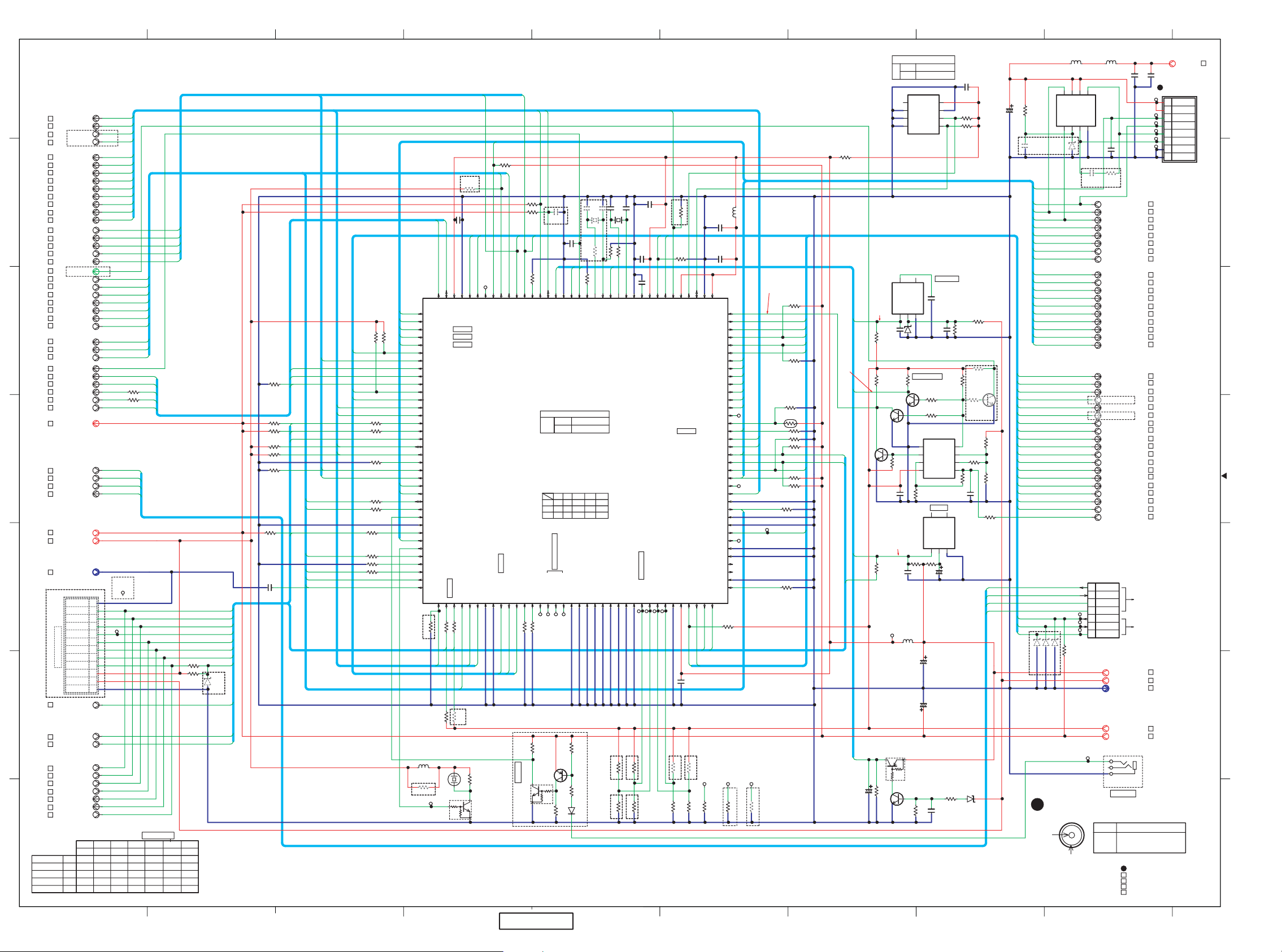
A
7
Main PWB(B2) section 5/6
[MICOM]
TUN-SCL
2
2
TUN-SDA
RDS-CLK
2
RDS-DATA
2
NX700E
2
VOL-SDA
VOL-SCL
2
2
DAC-RST-DVD
SYS-MUT
2
2
SUB-MUT
2ZONE-SENS1
Reserve
Reserve
Reserve
2
2ZONE-SENS2
2
2
2
3
3
3
3
3
NAVI-SYS-ACC
3
3
3
3
3
3
3
3
MOS-RST-DET
3
3
3
4
4
4
4
4
4
4
2ZONE-A
2ZONE-B
NAVI-MA
MA-NAVI
NAVI-RST
NAVI-MON
B/U9V-DET
TP-SCK
TP-SI
MOS-RST
MOS-SCL
MOS-SDA
DIMMER
ENAB
FL-ADJ
B/U-DET
USB-RST
USB-ACC
USB-SCL
USB-SDA
USB-REQ
REM3.3V
WP
6
5
4
B-RESET
4
4
BOOT
B-TX
4
B-RX
4
REM3.3V
6
REM5V
6
F-GND
6
NO USE
3
VOL DOWN
TO SW PWB
3
J501
F-GND
RESET
VOL UP
OPN/CLS
SOURCE
ILL-ON
BLK-LED
REM5V
B/U14V
BUF-DET
IR
2
SD-DET1
3
3
SD-DET2
RESET
3
3
VOL UP
3
VOL DOWN
SOURCE
3
3
ILL-ON
BLINK
3
3
1
QY-5014Y-A
QY-5015Y-A
U/K
TP556 TP557 TP558 TP559 TP997 TP998 TP999
H
USA
L
CAP
L
CA
BRA
H
L
EUR
M121
M127
M128
NO USE
TP539
1
2
3
4
5
TP540
6
7
8
9
10
11
12GND
IR
NTSC/
N_TEST
PAL
L
L
H
L
H
L
L
LH
HL
L
M23
M22
M73
M54
M55
M49
M50
M77
M78
R500
R501
M6
BOOT
B-RX
RST
B-TX
BRZ
M72
M70
M68
M71
M62
M61
M76
M28
M27
M119
M44
M45
M36
220
M35
220
M46
N9 OR N9PLUS
K:Exclude BRZ
E/U BRZ
L
L
-
L
-
L
-
L
NX700
E2P-SCL
E2P-SDA
AMP-REM
BACK-GEAR
VIDEO-RST
DVD-RST
DVD-ON3
DVD-ON2
FAN-TEMP
TILT-VR
SUB-MUTE
SYS-MUTE
SD-DET1
SD-DET2
TEL-IN
TEST-MODE
FL-ADJ
SYS-ACC
SOFT-TEST1
MS-P-SEL-B
MS-P-SEL-A
FLMD1
ILL-DET
AV/ILL-ON
M107
M105
M106
1
C517
NO USE
10K
R598
10K
R599
AVREF0
ACC-IN
AVSS
A-ANT
PKB
CDTI
CCLK
CSN
N.C.
OP/CL
N.C.
N.C.
N.C.
N.C.
N.C.
N.C.
BLK-LED
ILL-ON
TP997
C506
10
6.3V
C
C507
0.1
123456789101112131415161718192021222324252627282930313233343536
144
143
142
141
140
139
138
137
136
135
134
133
132
131
130
129
128
127
126
125
124
123
122
121
120
119
118
117
116
115
114
113
112
111
110
109
M108
(MEM3.3V)
0
R997
F
C
R550
10K
M138
M137
M136
M135
M134
M133
M132
M129
M126
M123
M119
TP998
0
R998
4.7uH
L501
TP531
NX700E
TP538
M128
M127
M121
TP536
TP999
0
R999
NO USE
ACC_ON: 3.5V
ACC_OFF: 0V
R561
TH501
R542
R540
R562
R564
R543
R566
TP537
R567
10K
R551
10K
R560
10K
10K
M143
M142
M141
M140
M139
10K
M124
M116
G
E2P-ROM-DATA
U/3RD
P
485-0107-06
R
N
EUR
485-0108-09
8
1
VCCA0
7
2
A1
WP
6
3
A2
SCL
5
4
GND SDA
IC507
S24CS04AFT-V-G
0
R537
(REM3.3V)
(MEM3.3V)
IC504
S-80931CNMC-G81
123
BATT Voltage Less than 5.9V: 0V
Normal: 3.4V
M19
C
0.01
C510
470K
R569
BATT Voltage Less than 8.8V: 0V
Normal: 5.3V
R572
100K
R570
M18
Q502
2SC4155A
0
10K
10K
22K
22K
M126
M125
RESET-SW_ON 0V
M14
M14
M21
16V
22
C531
Q503
2SC4155A
C512
100
R507
TP549
(VDD3.3V)
(REM3.3V)
Q504
RT1P241M
220K
R568
R571
1
C
C514
D504
MA8110M
100K
2SC4155A
100K
3.3VRESET-SW_OFF
R574
100K
C
0.047
L502
4.7uF
Q506
2SC4155A
R575
45
B/U9V DET
Q501
R576
R577
R573
R578
LZ
6.3V
C516
1000
6.3V
C518
47
47K
C532
C
5678
(F)
220
RESET
NC
OUT
123
5.6K
0.1
B/U DET
C509
C511
10K
10K
IC505
VDD
C
22p
1000p
NJM2078M
C
45
C515
R579
33K
NC
VSS
(B/U 9V-DET)
100K
R581
1234
IC506
16V
10
HZU6A2L
C
C520
0.1
R583
4.7K
R584
4.7K
R587
180K (F)
(F)
220K
R580
NO USE
R588
100K
R585
10K
Q512
2SC4155A
R586
1M
(F)
R582
3.3K
0.1
C
C513
BU4820G-TR
D516
H
R591
12K (F)
B-RX
B-TX
BOOT
RST
R589
R590
(F)
220K
(F)
33K
LZ
16V
100
C528
0
R544
C
NO USE
M7
M83
M47
M42
M48
M81
M140
M139
M143
M142
M141
M105
M82
M116
M31
M32
M106
M124
M26
M25
M8
NO USE
FIN
IC508
RIN
5678
BD6221F-E2
0.1
C529
D521
MA8075
M123
M29
M37
M38
M39
M40
M41
M129
M126
M60
M59
M132
M133
M134
M66
M135
M136
M137
M138
NO USE
NO USE
TP545
TP546
TP547
R593
D502
D503
D501
MA8056M
MA8056M
MA8056M
4
Steering wheel remote control terminal
(J506)
1
I
L551L552
mPZ2012S601AmPZ2012S601A
1234
VCC
VCC
OUT1
VREF
OUT2
GND
C
C533 R552
0.1 330
NO USE
M-PLS
MTR1F
MTR1R
MTR2F
MTR2R
MTR-PWR
TILT-VR
OP-PLS
MA-DVD
DVD-MA
DVD-ON2
DVD-ON3
DVD-RST
FL-ON
CSN
CCLK
CDTI
V-RST
AV-ON
F-SEL
AMP-STB
OFFSET-DET
AMP-MUTE
LCD-ON
PKB
BACK
ANT-ON
REM-ON
REM-DET
ILL-DET
FAN-ON
SYS-ACC
CENET-TX
CENET-RX
AV/ILL-ON
PHONE
ACC
(for Ver.Up connector)
P504
1
B-RX
2
B-TX
3
BOOT
4
RST
5
M-TX
6
M-RX
7 FLM
10K
3.3V
TP541
No.
1
2
16V
C
C
C534
10
TP550
TP551
TP552
TP553
TP554
C
TP555
0.1
C530
3
3
3
3
3
3
3
3
3
3
3
3
3
3
3
3
3
3
6
6
6
6
6
6
6
6
6
6
6
6
6
6
6
6
6
6
6
BOLERO
MASTER
J506
6
6
6
6
6
MEM3.3V
B/U14V
GND
VDD3.3V
REM3.3V
W-REM
Pin name
REMOTE CONT
SHIELD GND
MOTOR8V
16V
C535
10
g
To J5001 of Slide PWB
J502
1
MTR8V
MTR8V
2
OP/CL
3
PULSE
4
OUT1
5
OUT2
6
GND
7
GND8
J
6
7
6
5
4
3
2
1
2
g
: To page 46
: To page 41
2
: To page 42
3
: To page 43
4
: To page 45
6
BC
M26
M25
M58
M57
M43
(REM5V)
(REM3.3V)
USB-SCL
M37
37
MTR1F
M38
38
MTR1R
M39
39
10K
4.7K
R512
R511
R558
R592
R559
R554
R555
R541
R556
R557
R513
100
100
10K
100
100
100
100
10K
100
M42
M43
M44
M45
M46
R563
47K
10K
R594
M51
M52
10K
R595
M53
4.7K
R508
4.7K
R510
10K
R521
M61
M62
M65
R504
10K
C523
100p
C
M14
M51
M52
M74
M65
M107
M108
1K
R503
E/K
-
L
L
-
L
R502
100K
-
-
-
L
-
NO USE
D519
M53
MA8082L
M75
M126
M125
M68
M70
M71
M72
M47
M48
M49
M50
M54
M55
M57
M58
(REM3.3V)
MTR2F
M40
40
MTR2R
M41
41
MTR-PWR
42
OFFSET-DET
43
NAVI-SYS-ACC
44
USB-RESET
45
USB-ACC
46
USB-REQ
47
AMP-STB
48
AMP-MUTE
49
2ZONE-SENS1
50
2ZONE-SENS2
51
VOL-UP
52
VOL-DOWN
53
IR
54
VOL-SDA
55
VOL-SCL
56
N.C.
57
NAVI-MONI
58
NAVI-RESET
M59
59
DVD-MA
M60
60
MA-DVD
61
MOS-SDA
62
MOS-SCL
63
W-REMCOM
64
N.C.
65
SOURCE
M66
66
FL-ON
67
BEEP
68
TP-MA
69
N.C.
TP-SCK
70
MOS-RESET
71
72
WP
10K
R514
NX700
L503
220uH
R565
0
NO USE
D
M26
NO USE
R519
10K
C
0.1
C504
M36
M35
M32
M31
TP542
BUS-
BUS+
EVSS
EVDD
NO USE
NO USE
NO USE
2ZONE-A
MOSES-RST-DET
MOSES-BUF-DET
100
R517
M75
M77
M76
10K
R518
NO USE
(VDD3.3V)
2ZONE-B
M78
1K
R520
Q511
RT1N436M
NV-ON
N.C.
USB-SDA
NO USE
OPN/CLS
73 74 75 76 77 78 79 80 81 82 83 84 85 86 87 88 89 90 91 92 93 94 95 96 97 98 99 100 101 102 103 104 105 106 107 108
RDS-DATA
100
R516
M74
M73
10K
R515
X503
TP548
M29
R522
M28
M-PLS
N.C.
M81
22K
M27
M26
ENAB
DIMMER
NO USE
FAN-ON
PANEL-ON
M82
M83
M25
R538
4.7K
NAVI-MA
MA-NAVI
F-SEL
N.C.
10K
R523
W-REM
Q507
R539
4.7K
M23
M22
C519
M25
10K
R524
N.C.
T-SCL
T-SDA
MAIN
UPD70F3354GJ(A)-GAE-
99
100
102
N.C.(CLKOUT)
N.C.
RDS-TEST1
10K
TP532
TP533
R525
R526
100K
Q505
RT1N141M
C
22p
M21
CATS-DET
SOFTWARE CODE
U/3RD
EUR
(VIRGIN MICOM)
USA EU SEA AUS BRZ
HL L L
LHH H
RUNNING TEST
RDS-TEST2
TP534
ISA1602AM1
NO USE
C
C527
1000p
M19
N.C.
B/U6V-DET
470-2730-XX
470-2729-XX
IC503
V850ES/SJ3
N.C.
RDS-TEST3
TP535
R529
4.7K
R530
10K
R527
(MEM3.3V)
(REM3.3V)
X502
32.768KHz
C
NO USE
22p
C502
R536
M18
N.C.
B/U9V-DET
N.C.
N.C.
10K
D515
MA111
E
18p
C503
470
10K
R531
(Xtout)XT2
N.C.
3.145728MHz
C
C
M14
RESET
(Xtin)XT1
H
L
HLLLL
N.C.
N.C.
PAL
NX700E
NX700
X501
C521
0
R505
10K
R545
NTSC
10K
R546
C
12p
R509
(Xout)X2
N.C.
12p
C522
10K
(Xin)X1
N.C.
10K
R548
10K
R549
C501
6.3V
C505
0.1
C
C
VSS
REGC
EU: NO USE
US/3RD
N.C.
TP556
NX700
NX700E
C
10
C508
VDD
NTSC/PAL
TP557
M7
M8
6.3V
4.7
FLM
AV-ON
BRAZ/OTHER
NOISE-TEST
TP559
TP558
M6
10K
R506
R547
100K
RDS-CLK
NO USE
BVSS
C
10K
R596
10K
R597
AVREF1
AMP-REM DET
DAC-RST-DVD
BVDD
NO USE
A
BC
-
NX700/NX700E
E
F
G
H
I
J
Page 45
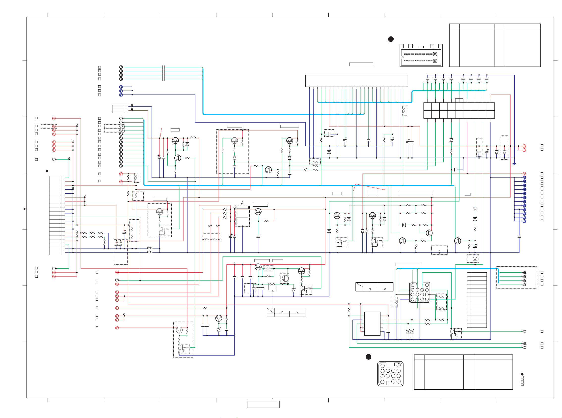
J
- 45
I
H
G
F
E
D
BC
A
Pin name
No.
REAR L-CH (-)
2200p
7.0V
N.C.
1
REVERSE GEAR
2
REAR L-CH (+)
3
PARKING BRAKE
4
FRONT L-CH (-)
5
N.C.
6
FRONT L-CH (+)
7
ACC
8
FRONT R-CH (+)
9
C
C
C
C
C
C
C608
C607
C606
C605
C604
2200p
FL+
7.0V
D602
MA111
(F)
R609
10K
C622
0.1
ACC
0
0
7.0V
AUTO
ANT
C
ILL-DET
0V
ILL+_HI
2SC4155A
2200p
FR+
7.0V
AMP
REMO
13.9V
0V
POWER_ON
POWER_OFF
ILL
3.5V
ILL+_LO
Q619
NX700
1
2
3
4
5
6
7
8
9
10
11
12
13 N.C.
F
Q627
RT1N436M
2200p
13.9V
POWER_ON
2200p
RR+
FR-
7.0V
ILL+PKBREV ACC
0V
NO USE
POWER_OFF
47K
R640
D623
MIF60
GND
B/U14V
L+
N.C.
N.C.
BUS+
R+
R-
SYS-ACC
BUS-
L-
N.C.
SHIELD-GND
7.0V
RR-RR+FR-FR+FL+FL-RL+RL-
BUS
+B
0.22
C618
P
D610
MA111
D615
MA8047M
R634
4.7K
25V
C630
33
2200p
RR-
C617
14.0V
BATT
GND
16V
2200
7
Main PWB(B2) section 6/6
1
Power supply connectorJ601
[Main connector,Power IC,Power supply block]
123456789101113
12
FL+
GND
FL+
16V
C610
47
POWER_ON
POWER_OFF
10K
R618
R626
1.2K
POWER AMP IC
TB2926HQ
RIPPLE
RL-IN
FL-IN
RL
FL
ANT-ON
MA111
D609
1/4W
3.3K
R644
IC601
S-GND
RR
3.3V
0V
001240390
D617
MIF60
J602
RR-IN
FR-IN
FR
C611
FR-
FR+
Q612
1/4W
1.5K
R637
FR+
RT1N436MRT1N436M
VCC
BUS+
BUS-
GND
R630
Q617Q616
NC
GND
1.2K
10K
R624
10
9
8
7
6
FR-
R605
1/4W
33K
VCC
AMP-MUT
AC-GND
1
C
3CG1260-Q
NX700 NX700E
IC605
LA2335
1
TXD1
2
TXD2
3
RXD
4
VDD
5
STBN
GND
RR-
MUTE
RR+
RR-
RR+
0V
3.5V
POWER_ON
POWER_OFF
50V
C612
1
REM/ANT+B CURRENT DET
REM-ON
REM-DET
MA111
D614
D618
MA111
ANT+B_REM+B short: 0V
Normal: 3.3V
CE-NET CONNECTOR
B-L+
B-R+
0
R652
NO USE
1
C
C640
DET
OFFSET
Normal: 5.1V
0
R621
16V
C613
2200
OFFSET
R615
1.5 1/4W
R620
1.5 1/4W
Q618
2SC4155A
D625
MA8180M
NO USE
P
0.22
C616
1.5 1/4W
1.5 1/4W
R631
3.3K
ISA1602AM1
22K
R639
B-L-
B-R-
71189
456
3
3.3V
D626
MA8180M
R616
R619
Q614
R638
3.3K
J602
C325
0.22
L602
L603
FAN-ON_HI
FAN-ON_LO
LZ
16V
C619
100
LCD5V(SW)
Q608
2SA1365
5.0V
560
R622
Q613
RT1N436M
8.5V
C
C
C
C
0.1
C620
C
C324
C327
C326
3.3V
0V
3CG1260-Q
0.22
0.22
0.22
FAN+B
Q601
R603
10K
R617
1.2K
NO USE
3.3V
ACC_ON
Q630
2SA1365
R651
47K
R601
Q605
2SC4155A
470
R613
LCD-ON
0V
ACC_OFF
1K
Q631
RT1N436M
AMP-FL
2
2
AMP-RL
2
AMP-FR
2
AMP-RR
2
6
4
USB5V
NX700
REM5V
2
REM5V
3
5
REM5V
REM3.3V
3
5
4
4
5
5
REM3.3V
REM3.3V
F-SEL
To J750 of D/D PWB
h
AV/ILL-ON
P602
REM3.3V
REM3.3V
GND
GND
GND
GND
AV-ON
GND
REM5V
GND
USB5V
DVD8V
DVD8V
P-GND
P-GND
+B
+B
+B
TP609
TP603
TP608
20F-SEL
19
18
17
16
15
14
13
12
11
10
9
8
7
TP606
6
TP607
5
4
3
2
1
3.4V
TP604
TP605
R696 R697 R698
56
1/4W561/4W561/4W
R699
33
1/4W
R693 R694
33
1/4W331/4W
3
5
AV/ILL-ON
3
MOTOR8V
MOTOR8V
5
2
4
5
2
5
5
3
2
2
4
3
2
AUDIO-GND
AUDIO-GND
4
5
5
5
OFFSET-DET
5
5
5
5
5
5
5
5
5
5
3
3
USB-B/U3.3V
MEM3.3V
VDD3.3V
VDD3.3V
S-GND
AMP-STB
AMP-MUTE
LCD-ON
PKB
BACK
ANT-ON
REM-ON
REM-DET
ILL-DET
ACC
PHONE
FAN-ON
LCD3.3V
LCD5V
1/4W
R695
33
NO USE
AV-ON
B/U4V
AV8.5V
DAC5V
DAC5V
FAN5V
P601
FAN-12
FAN+
LZ
16V
C633
100
16V
C632
C631
470
NO USE
NO USE
0
R648
16V
470
TP614
TP601
TP602
AMP-STB
AMP-MUT
LCD-ON
OFFSET
ANT-ON
REM-ON
REM-DET
ILL-DET
PHONE
0
R645
R685
R686
3.3V
4.1V
3.4V
3.5V
PKB
BACK
ACC
0
R649
NO USE
180
1/4W
R684
1/4W
NO USE
56
1/4W
56
mPZ1608S300A
mPZ1608S300A
NO USE
R610
47K
L601
22uH
D608
R650
MA111
10K
FL
RL
FR
RR
C639
NO USE
R688
0
6.3V
C
10
FL-
RL+
VCC
STBY
RL-
TAB
GND
1234567891011121314151617181920 21 22 23 24 25
FL-
RL+
RL-
0V
4.5V
PHONE DET REV/PKB DET
NO USE
D613
MIF60
TP610
R623R629
00
Q628
2SC5824
6.3V
C
C638
10
TP611
5.1V
5.6K
R627
PHONE
D611
MIF60
D616
MIF60
D624
MA8056M
Q602
ISA1602AM1
R606
4.7K
D601
MA111
0.01
C614
16V
C625
47
TP613
16V
C643
10
470
R625
16V
C
C637
10
C
SERVICE PART
TP612
B/U3.3V
IC602
AN77L04M
123
C
0.1
C626
16V
C
C
C642
10
47K
R602
Q620
2SC3420
16V
C634
10
C644
NO USE
C
16V
10
R607
47K
HEAT SINK
C
0.33
C671
HEAT SINK
16V
C635
10
C
C
0V
J601_REV_HI
BACK
Q634
2SB1375
R687
22
R635
NO USE
R636
C
C636
3.4V
J601_REV_LO
2SC4155A
0
680
R642
0
0.047
R642
0V
3.4V
5.6K
R628
J601_PKB_HI
J601_PKB_LO
Q607
R614
6.8K
PKB
AV8.5V
NO USE
G
100ǡ 0
Q604
ISA1602AM1
4.7K
R691
D603
MA111
C
C623
0.01
D
Q622
S
D620
HZS9B3L
Q622
47K
R692
NO USE
D606
MA111
Q621
ISA1602AM1
2SK0662MRL
Q623
RT1N436M
R643
R608
R611
R612
4.7K
R604
10K
10K
22K
10K
R641
C609
POWER_ON
POWER_OFF
NO USE
12K
D607
AMP-STB
3.3V
0V
ACC_OFF
ACC_ON
1
C
MA8030L
ANT+B REM+B
Q610
3CG1260-Q
D619
MIF60
C601
RL-
R632
10K
141516
2200p
7.0V
12
10
2131
R689
120
R690
120
C
C602
RL+
NO USE
C
2200p
7.0V
17
18
C603
FL-
TM601
NO USE
R653
R654
R647
68 1/4W
Pin name
No.
AUTO ANTENNA
10
FRONT R-CH (-)
11
AMP REMOTE
12
REAR R-CH (+)
13
ILLUMINATION
14
REAR R-CH (-)
15
BUS BACK UP
16
BACK UP
17
GND
18
J601
NO USE
D604
D605
1N5404
SM5S22A
NX700
B-L+
B-L-
B-R+
B-R-
ACC_ON
ACC_OFF 0V
C641
3.3V
100p
7
6
5
3
B/U14V
5
B/U14V
REM+B
GND
GND
GND
M-GND
M-GND
F-GND
F-GND
F-GND
V-GND
USB-GND
USB-GND
USB-GND
C
2
2
3
5
2
3
3
4
4
5
3
2
3
4
3
BUS-L+
2
2
BUS-L-
BUS-R+
2
BUS-R-
2
2
SYS-ACC
5
CENET-RX
CENET-TX
5
5
3
NO USE
1
J
I
H
-
NX700/NX700E
E
DG
CeNET terminalJ602
11
7
3
1
12
1098
654
213
No.
Pin name
1
GND
2
B/U +14V
3
BUS AUDIO L-CH (+)
4
N.C.
5
N.C.
6
BUS (+)
7
BUS AUDIO R-CH (+)
No.
Pin name
8
BUS AUDIO R-CH (-)
9
SYSTEM ACC
10
BUS (-)
11
BUS AUDIO L-CH (-)
12
N.C.
13
N.C.
BC
h
: To page 46
: To page 41
2
: To page 42
3
: To page 43
4
: To page 44
5
A
1
Page 46

F
- 46
G
H
Main PWB CONNECT
g
To J502 of Main PWB
J5001
8.0V
1
2
3
4
5
6
7
8
NORMAL:0V
OPEN:7.7V
NORMAL:0V
CLOSE:7.7V
3.4V
14.0V
Main PWB CONNECT
h
To P602 of Main PWB 6/6
TP750
TP751
TP752
TP753
J750
20 F-SEL
19 REM3.3V
18 REM3.3V
17 GND
16
GND
15 +B
14 +B
13 +B
MTR8V
MTR8V
OP/CL
PULSE
OUT1
OUT2
GND
GND
12 GND
GND11
10 AV-ON
9
GND
8
REM5V
7
GND
USB5V6
5 DVD8V
DVD8V4
3 AV/ILL-ON
P-GND
2
1 P-GND
5.1V
5.1V
8.1V
TP754
TP755
TP756
TP757
TP758
TP759
TP760
C758
1500p
C
L750
10u
D751
RB060L-40
13K
(F)
E
16V
10
C770
16V
10
C771
CCC
R802R754
1.5K
(F)
16V
10
C772
3.4V
14.0V
Q750
RT1N241M
L754
L755
R762
10
D
C
C751
C760
4.7 16V
CC
R804 1k
NO USE
0.022
3300p
C753
C
ACC ON:3.2V
ACC OFF:0V
C752
47p
C
R753
3K
R758
47K (F)
270
Q752
R756
NO USE
SP8K23
A
D/D PWB(B3) section Slide PWB(B4) section
7
C754
33p
C
R755
6.2K
(F)
(F)
C
R759
68K (F)
R794R757
560
R760
300
6
12K
C756
1500p
4.7 16V
5
L751
22u
16V
16V
16V
10
10
C763
10
C764
CCC
C765
NO USE
D750
RB060L-40
BC
(F)
9.1K
R750
(F)
56K
R751
(F)
3.3K
R796
RT
N.C
N.C
N.C
SYN.C
D/D
IC750
BD9017KV-E2
CL2
BOOT2
C767 C768
1000p 1000p
0.082
N.C
N.C
VCCCL2
C C
25V
25V
10
10
100
R765
C774
C773
(F)
C
GND
VCC
C
N.C
N.C
VCCCL1
N.C
100
R766
R771R769
0.039
(F)
EN2
COMP1
VREG5A
DGND1
CL1
252627282930313233343536
N.C
EN1
N.C
SS1
FB1
N.C
N.C
N.C
N.C
OUTL1
BOOT1
OUTH1
24
23
22
21
20
19
18
17
16
15
14
13
SW1
C769
0.033
R806 10k
NO USE
C755
2200p
C
C
C757
1 25V
C759
Q751
SP8K23
C750
0.022
C
R752
470K
SS2
37
PGOOD
38
COMP2
39
FB2
40
N.C
41
EXTVCC
42
N.C
43
N.C
44
VREG5
45
N.C
46
OUTL2
47
DGND2
48
SW2
R761
10
C C
C766
0.033
R805 10k
NO USE
OUTH2
123456789101112
4
5.1V
L756
(F)
9.1K
N.C
SYN.C
CL2
BOOT2
R772
(F)
56K
R773
(F)
3.3K
R797
RT
N.C
N.C
D/D
IC751
BD9017KV-E2
N.C
VCCCL2
N.C
GND
VCC
N.C
N.C
VCCCL1
N.C
EN2
COMP1
VREG5A
DGND1
CL1
252627282930313233343536
N.C
EN1
N.C
SS1
FB1
N.C
N.C
N.C
N.C
OUTL1
BOOT1
OUTH1
SW1
ACC ON:3.2V
ACC OFF:0V
C
C776
24
23
22
21
20
19
18
17
16
15
14
13
R784
10
C785
4.7 16V
CC
R807 1k
NO USE
0.022
2200p
C780
C
C779
33p
C
R782
560
R777
4.7K
C783
820p
C
L753
10u
9.1K (F)82K (F)
R779
10K
(F)
R795R781
Q753
8.1V
RT1N241M
L757
C
C775
0.022
R774
470K
C777
33p
R775
6.2K
C
C778
2200p
C
C
C782
1 25V
C784
4.7 16V
R783
10
SS2
37
PGOOD
38
COMP2
39
FB2
40
N.C
41
EXTVCC
42
N.C
43
N.C
44
VREG5
45
N.C
46
OUTL2
47
DGND2
48
SW2
OUTH2
123456789101112
3
R803R776
68K (F)
C
C781
1000p
R778
470
(F)
R780
330
12K
(F)
2
L752
22u
14.0V
L758
25V
10
C798
C
25V
10
C799
C
C793
1000p
R788
R793R791
0.039
(F)
100
C794
0.033
R809 10k
NO USE
Q755
SP8K23
NO USE
D753
16V
16V
10
10
C796
C795
RB060L-40
16V
10
C797
CCC
C792
16V
16V
16V
10
10
10
C790
C788
C789
CCC
1
D752
RB060L-40
NO USE
Q754
SP8K23
C C
C791
0.033
R808 10k
NO USE
1000p
C C
100
R787
0.039
(F)
TP5001
TP5002
TP5003
TP5004
C
330
R5603
0.1
C5603
560
R5621
PULSE
21 2
IC5604
GP1S93
PHOTO INTERRUPTER
0.1
NO USE
C5637
P5603
1
OUT1
2 OUT2
P
SLIDE MOTOR CONNECT
I
NORMAL:3.3V
OP/CL:0V
560
1/4W
1/4W
R5625
1
IC5606
GP1S93
3443
WHT
ORG
OP/CL
To Slide Mech
J
7
6
5
4
3
2
1
5.1V
L759
g
: To page 45
h
A
BC
-
NX700/NX700E
E
F
G
H
I
: To page 44
J
Page 47

J
I
PRINTED WIRING BOARD
Panel PWB(B1) section
7
Panel PWB has four layers.
*
IC
Q
Q113
Q110
IC104
Q100
Q109
6
5
4
3
2
1
Q108
Q107
Q102
Q902
Q901
Q701
IC105
IC701
IC703
IC702
TM103
R119
TM100
C116
C127
C118
D109
C211
L128
C121
R123
D102
R102
C201
Q107
C210
C209
C208
R121
L129
C115
C130
R111
R114
H
C134
R261
L109
R183
C202
L113
R139
C131
R108
C217
C218
Q110
L130
R131
D100
R170
C112
R105
Q113
C124
C119
Q109
L119
L118
L117
R171
C140
R133
L116
C139
R137
C141
L112
L120
C150
C153
C717
IC701
T701
C702
1(HIGH)
PNK
Q108
D112
C142
C216
C136
IC703
P701
R208
R141
D113
C157
2(LOW)
L102
C104
L108
C122
D114
R144
C213
C214
C714
C715
C701
D704
WHT
Q100
R253
D115
C162
C160
16
C708
C704
Q701
C706
L141
C205
R145
C161
L138
IC702
1
9
10
16
C206
C196
C195
R136
R250
C709
C707
D701
C848
C703
IC104
C198
C191
R264
L137
9
8
R721
C705
R714
G
8
5
1
L132
L131
C171
C170
R200
R199
R702
C713
C711
C716
R712
R701
D703
R713
D105
R221
L134
L133
C178
R217
R215
R201
L135
C177
L124
R715
R716
D103
L136
C174
L122
D106
D104
CCT105
CCT106
C203
C175
C204
C172
C193
C190
C188
C189
C192
C181
C182
L125
R218
R216
C215
L103
C720
C721
R177
C176
C183
L106
L105
L104
C727
C726
C725
L701
R707
R708
TM102
R157
R160
4
R158
5
L123
Q902
Q901
C168
IC105
R188
C194
L127
R213
L702
L703
D116
R161
1
8
R194
L126
L110
TM101
R159
C180
R182
C187
C262
C197
C207
C257
F
D107
S901S902S904
R262
R263
Q102
S903
D903D905 D904 D902
VOL DOWN RESETSOURCE VOL UP
IR901
Panel PWB-B(B1) Panel PWB-B(B1)
E
D909
R905
R904
R903
D911
D910
R906
15 1
R907
D912
C901
R902
R901
J901
14 2
D901
c
b
To LCD
TP163
TP171
TP141
TP127
TP126
TP125
TP124
TM105
J105
d
To Touch panel
TP170
R128
Q112
TP139
TP153
TP128
1
TP138
16
TP129
D
1
J104
30 1020
TP137
(BU14V)
R185
TP108
TP130
TP132
TP133
TP134
TP140
(REM5V)
TP136
(ILL8V)
TP172
L107
C173
TP168
R179
R178
TP169
5010 20 30 40
1
F701
TP712
J102
TP151
C179
TP162
R166
R165
R180
J103
TP711
R202
14
89
R181
TP179
132
C169
TP144
TP131
TP107
TP810
TP808
TP710
TP770
TP708
R153
C156
L142
C159
R149
C165
R254
C158
R150
R205
TP150
TP149
TP148
R146
R255
L143
CCT102
R252
L115
CCT107
R197
TP147
CCT104
C167
88
90
100
110
IC103
120
130
140 150 160 170
133
TP143
TP142
R198
TP152
C166
Q105
L140
TP135
TP110(LCD5V)
TP109(LCD5V)
TP106
TP105
TP111
TP771
C712
R705
R706
R703
R711
C710
R709
Q702
TP704
Q705
C724
R720
TP713
TP154
L121
D108
R155
R206
R204
C164
L139
TP116
TP114
TP809
(3.3V)
C212
Q106
R126
R147
C126
R103
R203
R152
TP117
TP115
C109
C152
R151
Q104
TP118
TP113
TP701
TP706
(LOW)
R154
R110
R109
TP156
50607080
C151
R140
C149
X101
TP119
TP112
TP707
TP157
C135
D101
TP173
R172
45
40
30
20
10
176
TP807
TP702
TP703
(HIGH)
TP177
R127
R260
Q103
C125
R124
L111
R106
C199
44
R101
C138
C128
C147
R132
C137
C145
1
TP705
C186
C200
C144
C143
C148
C108
TP155
R169
R173
R168
R163
L114
R120
C120
C117
TP122
TP123
TM104
TP120
R125
C132
(1.8V)
R115
TP121
R118
R116
C219
C111
R117
C129
BC
IC
Q
A
7
TEST POINT
TP177(VGL-12V)
TP172(VCOM)
Q106
TP173(VGH+18.5V)
Q103
6
TP151(OP9V)
TP155(LCD1.8V)
TP162(LCD3.3V)
IC103
5
TP168(B)
TP169(G)
TP170(R)
Q112
Q104
TP171(LCD5V)
Q105
4
3
Q702
2
Q705
1
i
J
I
H
COMPONENT SIDE
-
NX700/NX700E
E
a
To J452 of Main PWB
DG
To LCD back light
Panel PWB-A(B1)
Panel PWB-A(B1)
SOLDER SIDE
: To page 49
a
BC
A
Page 48
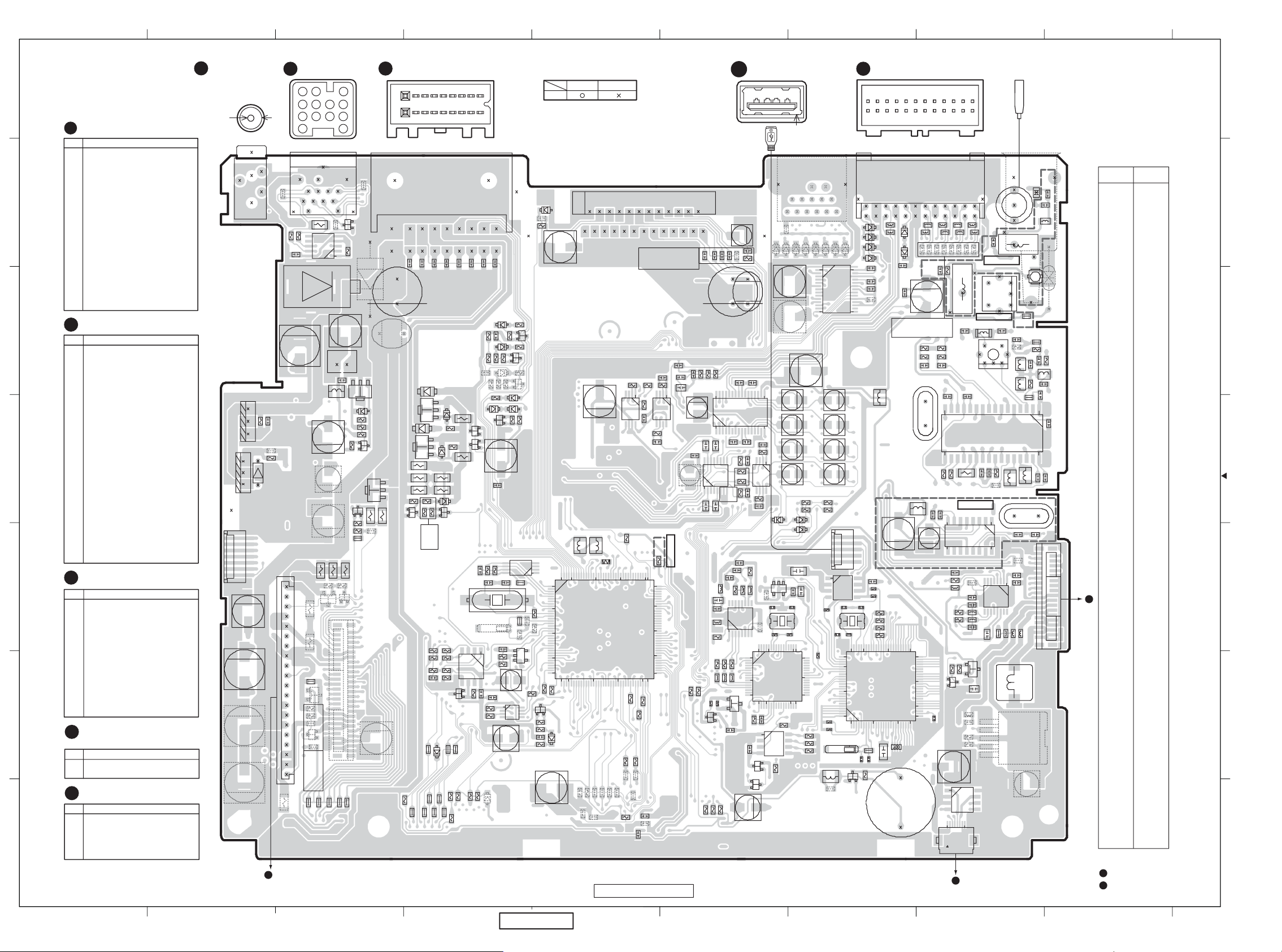
A
- 48
7
Main PWB(B2) section 1/2
* Dotted line parts are not used
in this model.
1
Power supply connector(J601)
No.
Pin name
1
REAR L-CH (-)
2
REVERSE GEAR
3
REAR L-CH (+)
4
PARKING BRAKE
5
FRONT L-CH (-)
6
6
5
4
3
2
N.C.
7
FRONT L-CH (+)
8
ACC
9
FRONT R-CH (+)
10
AUTO ANTENNA
11
FRONT R-CH (-)
12
AMP REMOTE
13
REAR R-CH (+)
14
ILLUMINATION
15
REAR R-CH (-)
16
BUS BACK UP
17
BACK UP
18
GND
2
RCA connector(P203)
No.
Pin name
1
LINE OUT REAR L-CH
2
LINE OUT REAR R-CH
3
LINE OUT FRONT L-CH
4
LINE OUT FRONT R-CH
5
S-GND
6
S-GND
7
SUB-WOOFER L-CH
8
SUB-WOOFER R-CH
9
S-GND
10
S-GND
11
2-ZONE L-CH
12
2-ZONE R-CH
13
REAR VIDEO OUTPUT GND
14
VIDEO INPUT-1 GND
15
REAR VIDEO OUTPUT
16
VIDEO INPUT-1
17
AUX INPUT-1 L-CH GND
18
AUX INPUT-1 R-CH GND
19
AUX INPUT-1 L-CH
20
AUX INPUT-1 R-CH
21
VIDEO INPUT-2 GND
22
CCD CAMERA GND
23
VIDEO INPUT-2
24
CCD CAMERA INPUT
3
CeNET terminal(J602)
No.
Pin name
1
GND
2
B/U +14V
3
BUS AUDIO L-CH (+)
4
N.C.
5
N.C.
6
BUS (+)
7
BUS AUDIO R-CH (+)
8
BUS AUDIO R-CH (-)
9
SYSTEM ACC
10
BUS (-)
11
BUS AUDIO L-CH (-)
12
N.C.
13
N.C.
4
Steering wheel
remote control terminal(J506)
No.
Pin name
1
REMOTE CONT
2
SHIELD GND
6
USB terminal(P702)
No.
Pin name
1
VBUS
2
USB D (-)
3
1
USB D (+)
4
GND
5
SHIELD GND
9
C606
R618
R624
R639
Q503
D391
R367
R368
C605
D609
R626
Q617
D614
R630
R615
R620
D618
Q618
X501
R376
R502
R366
R382
D
C604
C614
IC505
R377
R503
3456789101113
C603
R628
R691
R627
R609
D610
Q619
C522
R571
R389
R388
R516
2
1
C602
C623
R560
D603
R692
R606
R602
Q616
C520
X502
1
R515
210
1
C601
D606
D601
R583
R584
C521
C514
R578
C512
C387
D519
C630
C622
1
R574
1
C531
R614
Q604
D602
D615
IC507
R505
C502
C515
R384
R612
Q607
R611
R608
Q602
R640
R537
C503
IC506
Q385
IC381
C388
R396
R634
1
R509
R536
36
C455
BC
4
Steering wheel
3
CeNET terminal
1
Power supply connector
remote control
12
14
18
17
D605
C618
Q601
C451
18
17
C617
Q610
D617
Q612
R637
R616
R619
R632
R453
R452
R589
R590
R591
C513
16
15
Q614
R586
R581
R582
R573
R381
C608
D619
R631
R379
J601
C607
R638
R383
R369
R370
terminal
1
Q620
2
1
2
3
J506
R687
C671
Q634
R635
R636
D620
1
P504
7
(for Ver.Up connecter)
C633
C516
P602
C631
C632
h
To J705 of D/D PWB
2 13
6 5 4 3
10
12 11
R653
R647
R689
R690
C640
D604
C703
R650
1
R686
5
R685
R648
Q608
10
15
R617
R622
R649
20
Q613
R345
R684
R371
9 8 7
J602
132
3
456
7
8910
1112
IC605
P601
C620
L601
C625
R696
R697
Q630
R373
R372
1
R654
1
C619
J451
R374
1
R698
R651
R375
Q627
R473
R472
R471
R652
R644
(for FAN)
D608
R603
R601
R613
R610
Q605
Q451
Q452
Q631
R470
E
NX700 NX700E
J602
D607
C609
R604
R397
R398
113
C610
L502
L501
144
1
10
20
30
R501
130140
IC503
(CPU)
40 50 60 70
37
R500
D389
R454
R518
C454
C452
C453
COMPONENT SIDE
IC601(POWER)
C327
C236
R246
R264
R255
1
C263
TH501
R455
R456
R517
IC207
R458
R550
R511
R457
109
110120
100
90
80
72
R558
R556
R459
C523
R263
IC205
C243
R559
R557
R460
C460
C458
Main PWB(B2)
C324
C325
R244
C234
R506
108
73
1
C611
R605
R621
C326
C219
C217
C256
C255
NX700
C218
C288
R510
R508
Q703
F
24212
25
R203
R204
C211
R207
32 17
1
C207
IC208
R281
1
R282
C210
C208
C756
C743
C744
L707
C741
C740
L708
R737
R766
L703
L702
L701
R708
R707
R504
R594
C613
C282
IC209
C283
C209
R283
R752
IC704
1
R768
Q701
C707
R595
6
C612
C285
R294
C227
R284
R767
16
R717
Q706
Q707
C518
USB terminal
4
1
2
3
R349
D388
D387
C427
C616
C422
C284
16
C303
1
IC212
R331
R293
C302
R751
L705
64
10
20
17
1
C763
C714
R738
R715
60
IC703
(DSP)
D363
IC702
R782
IC709
R332
50
30
R779
R780
R781
R783
C228
L706
1
C715
C759
5
D382
C258
C747
1
C713
X701
R714
49
40
32
J381
D381
C299
C295
C298
C301
D361
D362
48
33
R741
R740
L503
R565
D384
1
14
C708
C709
R753
R742
D383
1
C734
X703
C738
X702
D386
R333
R334
76
100
G
D351
D352
D385
D356
D355
IC421
C296
C297
C294
C300
1
P702
5
IC706
75
80
90
1
2
RCA connector
24
212223
24
23
L219
L218
C432
16
C433
C435
C434
15
C750
R754
R755
C735
R734
R732
R731
R736
R730
6070
IC705
(USB-CNT)
10 20
R739
C731
C730
R520
Q511
C323
C320
R222
R224
C221
L205
L209
C253
CCT708
C723
X503
13
P203
L217
D353
D354
C246
C321
C318
51
40
30
25
H
Radio ANT Jack
121214151617181920
11
L216
C319
50
26
10
C269
C245
C317
X101
C268
C273
R200
L206
2
3456789
1
2
L213
L214
L215
R225
C315
R339
R338
C722
1
L210
L212
L211
L202
NX700
L103
C106
C314
C316
R221
R223
L107
C220
C123
C112
IC101
17 18
R105
C117
R106
R107
NX700E
C261
C264
8
IC210
9
C202
C206
Q402
L410
C403
R404
R405
C528
1
18
J502
10
R337
L208
L207
C205
Q401
R402
R403
C401
IC508
g
To J5001 of Slide PWB
ANT201
C250
NX700E
ANT202
L204
C104
R104
C119
R112
1
C265
IC200
R401
C204
1
1
5
L201
R230
C200
R202
L101
L102
R103
R108
L105
R408
C408
C272
L408
L409
IC401
ANT200
C102
L106
X131
L411
L412
C402
SUP201
C249
C248
L200
R245
R101
C101
L104
C108
C105
116
C114
C271
J401
SUP200
R102
C107
C115
I
IC
IC601
Q627
IC605
IC421
Q607
Q604
Q602
Q601
IC207
Q610
IC205
Q619
IC209
Q634
IC101
Q616
Q617
Q605
Q612
IC212
Q620
IC208
Q451
Q452
Q614
Q618
IC210
IC507
IC706
To DVD mech
e
IC702
IC200
Q630
Q631
IC704
IC503
IC506
IC505
Q401
IC703
Q402
IC705
Q503
IC381
Q608
Q701
Q385
Q703
IC401
Q613
IC709
Q706
Q511
Q707
IC508
g
: To page 50
: To page 50
h
J
7
Q
6
5
4
3
2
1
A
BC
-
NX700/NX700E
E
F
G
H
I
J
Page 49

J
- 49
I
H
G
F
E
D
BC
A
7
Main PWB(B2) section 2/2
7
* Dot-line parts are not used in this model.
* Dash-line parts are the parts on a component side.
TP385
TP389
Q203
R330
TP711
TP720
C746
R763
R756
TP707
TP716
R743
C733
R760
C749
TP548
TP997
TP998
TP999
TP382
TP384
C431
Q205
Q206
Q209
Q222
Q221
TP709
R777
C737
IC707
1
J381
TP381
TP392
L421
C222
C223
C224
Q208
Q204
Q207
Q210
Q220
Q219
C745
R713
R712
R744
TP388
C429
C430
C436
C421
Q704
R757
TP702
R748
R749
TP383
TP390
TP387
R306
R290
R305
R298
R286
R297
R303
R289
R304
R292
R310
R309
R774
R711
R710
C711
C704
C701
R750
TP386
C428
R205
R206
R329
Q217
C710
R709
C755
C742
L704
C712
C719
R718
R719
R720
TP705
C290
R208
TP219
C291
C212
C293
R336
R776
R724
C702
R252
R280
C260
R279
C304
C305
R319
R323
R327
R328
R324
R320
TP701
Q702
R716
C717
C720
R725
C762
TP497
TP490
TP220
R254
R251
R276
R277
R325
R326
C716
TP713
IC701
TP488
R253
R227
Q213
Q214
NX700E
NX700
Q705
C718
R723
R773
1
R772
TP717
TP503
TP502
C279
TP221
R243
R229
TP557
TP534
R238
R237
TP223
R239
R231
R235
R233
R242
R226
R220
NX700
Q211
R321
R322
Q212
C757
NX700
TP706
TP505
TP504
TP486
1
R236
C287
Q215
Q216
R596
R598
R545
R548
TP533
TP532
C705
C706
R704
R705
R702
R701
R778
R703
R706
TP507
TP508
TP506
TP393
R232
Q201
R275
R278
Q202
R566
R567
R597
R599
R546
TP559
TP556
TP558
TP535
R525
R523
R592
R514
TP494
TP498
TP479
TP478
TP484
TP509
TP483
TP482
TP480
10 20 30 40 50
Main PWB(B2)
C251
C252
C257
C280
C232
R354
R353
C231
C517
R549
R530
R529
R527
R555
R554
TP481
TP475
TP476
J452
TP391
R261
C262
C238
R312
R311
C237
TP537
TP536
NX700
NX700E
R526
Q505
Q507
TP511
TP510
NX700
R260
D262
D261
R355
R352
TP531
R543
R562
D515
R519
TP512
TP460
TP472
R540
TP538
R542
R561
C501
C508
R531
C527
C519
R541
R522
TP469
TP513
TP468
R607
R551
C505
R524
C504
R563
R513
R512
TP457
TP459
TP458
R234
R247
C213
C216
R240
C214
R241
C215
R256
R257
C254
R259
R258
C233
C229
R350
R357
R356
C235
R360
R359
C230
R358
TP224
C507
R547
C506
TP549
R507
D504
IC504
R593
C509
R568
R394
R395
Q384
R575
Q504
Q383
R392
R468
TP467
1
C532
R399
C456
Q506
R391
C457
TP542
TP493
D390
R521
R361
TP454
TP451
TP463
TP465
a
To J103 of Panel PWBa
210
1
C641
C511
R580
R587
R569
C510
R579
Q502
Q501
Q512
D516
Q381
Q382
C386
R390
TP540
NX700E
TP539
112
P203
IC
Q
TP209
TP212
TP217
TP204
TP202
TP206
TP208
TP205
TM103
L222
R538
R539
C292
L221
C259
R215
Q404
R407
NX700E
C760
C761
TP551
TP552
TP222
TP07
R115
C758
C409
C410
TP710
L552
R564
C530
12
11
R421
TP207
R423
C275
D421
D422
NX700E
TP614
TP708
C535
C534
L551
NX700E
6
L203
C247
NX700
2
1
ANT201
TP201
C322
TP200
TP203
5
TM102
C113
R216
L401
TP404
TP413
TP417
TP422
TP401
TP436
C109
C110
NX700E
L402
TP405
L413
L404
L405
L406
L407
TM101
L403
TP407
C406
C405
Q403
L108
C111
C116
C266
R267
R212
R268
R409
R410
R411
R412
C407
D521
C529
C120
C118
C203
C404
L491
C491
C492
R544
R211
L220
C274
R406
IC491
TP550
TP553
TP554
C533
L109
C121
C122
L223
NX700E
R552
TP555
Q208
Q205
Q204
Q206
IC602
Q203
Q207
Q622
Q213
Q211
Q215
Q216
Q201
Q202
TP402
TP403
TP408
TP411
TP415
TP420
TP424
TP431
4
Q209
Q210
Q623
Q621
Q222
Q220
Q212
Q214
Q628
Q219
Q217
Q221
Q218
3
Q704
Q702
Q705
Q502
IC504
IC708
IC701
2
IC707
Q505
Q507
Q501
Q404
Q506
Q403
Q384
Q383
Q512
Q504
Q381
Q382
IC491
1
TP211
C721
C724
TP210
R424
R425
R116
C124
TP718
C752
R729
R728
R727
R726
TP704
R722
C725
R422
C423
R761
C751
C736
C726
C727
R997
R998
R999
TP214
23
TP213
TP215
C425
NX700E
R769
IC708
1
R758
TP715
R746
TP714
C739
C728
R721
C732
24
TP216
C424
C426
R429
NX700
R300
R287
R299
R301
R288
R302
R296
R285
R295
R308
R291
R307
R335
D703
TP719
R762
R733
R745
R747
C729
R431
Q218
R735
R759
SOLDER SIDE
J501
R570
R577
R572
R576
R588
R585
R387
TP609
J601
9
R386
C385
R385
18
17
TM601
R451
R469
R380
R365
R362
TP471
TP358
TP352
TP353
1
11 12
TP602
TP601
R629
D611
D613
D616
R623
TP611
TP492
R364
TP496
TP499
R363
TP473
C459
TP357
TP361
TP355
TP351
1 12 24
TP354
J602
13 2
3
45 6
7
8910
D625
D626
TP612
Q622
C626
TP610
C644
C635
R643
R688
D624
C637
C638
L602
L603
TP606
TP500
TP495
TP474
TP470
R645
TP364
TP362
TP365
TP360
TP363
TP366
TP359
J382
f
To Navi PWB Assy
D623
NX700
1
2
3
TP541
R641
R625
C639
TP367
IC602
R642
Q623
Q621 C636
TP613
Q628
TP545
TP546
TP603
TP608
J506
1
3
C634
C642
C643
TP547
D503
D501
D502
TP604
TP607
TP368
TP371
TP374
2
TP605
R695
R694
R693
R699
: To page 47
a
6
5
4
3
2
1
J
I
H
-
NX700/NX700E
E
DG
BC
A
Page 50
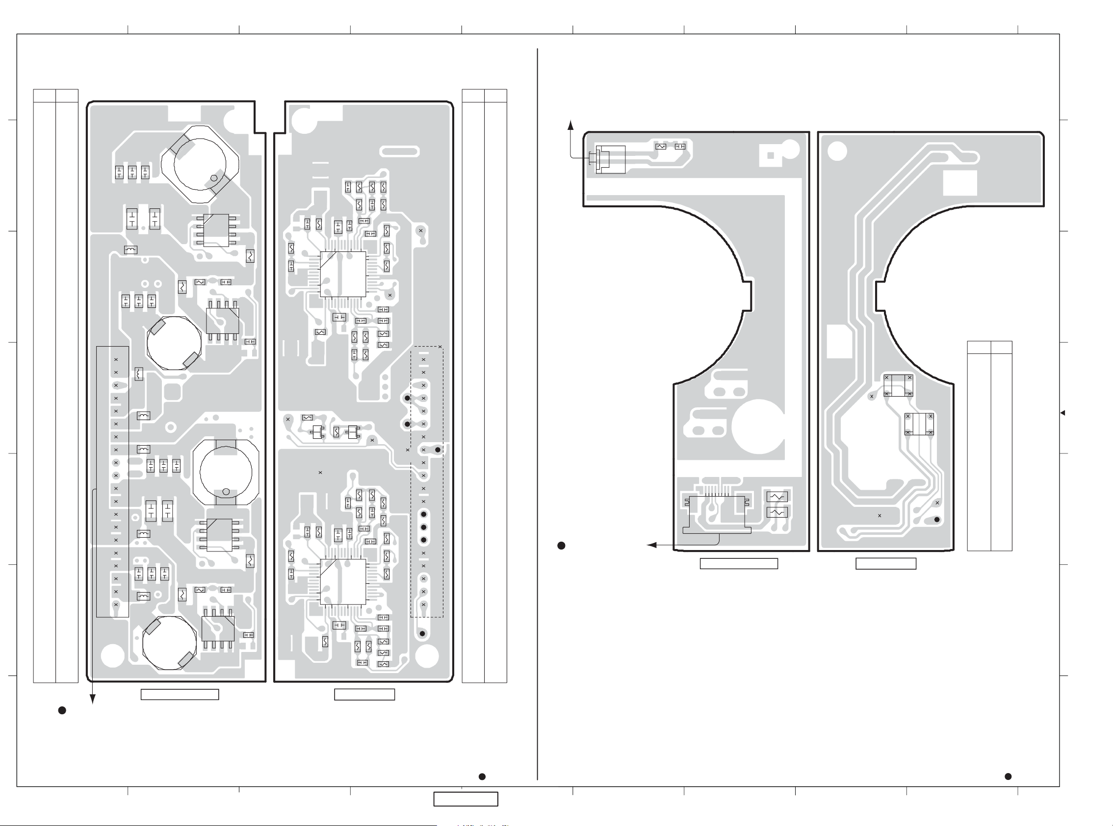
A
- 50
D/D PWB(B3) section Slide PWB(B4) section
7
D/D PWB has four layers.
*
BC
D
E
ICQ IC Q
To Slide Mech
WHT
C790
C789
C788
6
L752
C781
R778
R775
R803
ORG
F
C5603
R5603
1
2
P5603
G
H
I
J
7
6
C778
36
25
R781
R795
R776
R774
R773
R797
TP759
C776
C780
R777
R779
TP753
TP760
151015
IC751
IC5606
(OP/CL)
5
IC Q
C784
IC751
20
40
R780
C777
C775
C782
37
30
24
R783
C791
C798
Q754
5
C799
L758
C795
C796
C797
R793
R788
Q754
C793
R791
R787
C792
12
48
1
10
13
C779
Q755
L753
15101520
Q755
C794
R784
C785
R782
C783
L757
4
L759
L756
R750
TP750
Q750
Q753 Q753
R772
TP758
(DVD8V)
TP757
(USB5V)
TP756(REM5V)
Q750
TP5002
IC5606
IC5604 IC5604
(PLUSE)
4
TP755
L751
C765
C764
L755
C771
C763
C772
C774
R766
Q751
C768
R769
R765
C767
J750
3
C773
Q751
C770
L754
R771
2
Q752
Q752
C769
L750
C766
1
12
C760
TP752
R761
48
10
13
R762
C759
IC750
20
C756
R760
C757
40
C752
R758
C758
R759
C754
C750
37
30
24
R755
C755
36
25
R756
R794
R757
R752
R751
R796
C751
C753
R753
R754
R802
J750
(+B)(+B)(+B)
20
TP751
(REM3.3V)
IC750
g
To J502 of Main PWB
R5625
8
1
J5001
COMPONENT SIDE
R5621
Slide PWB(B4)
TP5004
SOLDER SIDE
TP5003
TP5001
(MTR8V)
3
2
COMPONENT SIDE
h
To P602 of Main PWB
1
A
BC
D/D PWB(B3)
-
SOLDER SIDE
h
NX700/NX700E
: To page 48
E
1
g
: To page 48
F
G
H
I
J
 Loading...