

Page 1

Xiamen Clarion Electrical Enterprise Co., Ltd
8/F., Xiamen Mail Processing Centre, No.275 Lujiang Road , Xiamen,China
Tel:+86-592-2389080 Fax:+86-592-2389089
Clarion Co., Ltd.
7-2, Shintoshin, Chuo-Ku, Saitama-Shi, Saitama 330-0081, Japan
Service Manual
Published by Service Dept.
298-6878-00
Printed in P.R.C.
JAN.2011 P
(PE-3402B-A)
This product is a lead free model.
Lead free solder is used in PWB stamped LF mark.
Please keep the following conditions when you repair.
1. Use lead free solder.
* Koki's lead free solder S3X-55M 0.6mm
(CLARION Parts No.642-0231-01)
* Koki's lead free solder S3X-55M 1.0mm
(CLARION Parts No.642-0231-02)
2. Use a nitrogen solder system.
3. Do not use "General solder" and "Lead free solder"
together.
SPECIFICATIONS
FM tuner section
Frequency range: 87.9MHz to 107.9MHz
(PE-3402B-A/B)
87.5MHz to 108.0MHz
(PE-3402K-A/B)
Usable sensitivity: 11dBuV
50dB quieting sensitivity: 17dBuV
Alternate channel selectivity: 60dB
Stereo separation: 30dB(1kHz)
Frequency Response: 30Hz to 15kHz(+3/-3dB)
AM tuner section
Frequency range: 530kHz to 1710kHz
(PE-3402B-A/B)
531kHz to 1629kHz
(PE-3402K-A/B)
Usable sensitivity: 28dBuV
CD player section
System: Compact disc digital audio
system
Usable discs: Compact disc
Frequency response: 20Hz to 20kHz(+1/-1dB)
Dynamic range: 80dB(1kHz)
2-DIN
Bluetooth CD/USB/MP3/
®
WMA RECEIVER
Model
Model
Model
Harmonic distortion: 0.03%
MP3/WMA mode
MP3 Sampling rate: 8kHz to 48kHz
MP3 Bit rate: 5kbps to 320kbps / VBR
WMA Bit rate: 5kbps to 320kbps
Logical format: ISO9660 level1, 2
JOLIET or Romeo
Bluetooth
Specification: Bluetooth Ver. 2.0+EDR
Profile: HSP(Headset Profile)
PBAP(Phone Book Access Profile)
HFP (Hands-Free Profile)
OPP (Object Push Profile) Phone
Book
A2DP (Advanced Audio Distribution
Profile)
AVRCP (Audio/Video Remote
Control Profile)
Send/Receive Sensitivity: Class 2
Audio section
Maximum power output: 50Wx4
Bass control action: +14/-14dB(100Hz)
Treble control action: +14/-14dB(10kHz)
Line output level: 4V(CD 1kHz) (PE-3402B-A)
2V(CD 1kHz)
(PE-3402B-B/PE3402K-A/B)
General
Power supply voltage: 14.4V DC(10.8 to 15.6V allowable),
negative ground
Current consumption: Less than 15A
Speaker impedance: 4ohm(4ohm to 8ohm allowable)
Auto Antenna Rated Current: 500 mA or less
Weight: Source unit 1.52kg
Remote control unit 40g
(PE-3402B-A)
Dimensions(mm): Source unit
178(W)x100(H)x155(D)
Remote control unit
44(W)x113(H)x11(D) (PE-3402B-A)
CX501
(PE-3402B-A for USA )
CX501B
(PE-3402B-B for BRAZIL )
CX501A
(PE-3402K-A for Australia)
(PE-3402K-B for Asia)
-1-
CX501/CX501B/CX501A
Page 2

MECHANISM SERVICE MANUAL
Please refer to the following service manual for the
CD-mechanism.
Mechanism No. Manual NO.
929-5110-80 298-6885-00
NOTES
We cannot supply PWB with component parts in principle. When
*
a circuit on PWB has failure, please repair it by component parts
base. Parts which are not mentioned in service manual are not
supplied.
Specifications and design are subject to change without notice for
*
further improvement.
Use only compact discs bearing the or mark.
*
Some CDs recorded in CD-R/CD-RW mode may not be usable.
* “Made for iPod,” and “Made for iPhone” mean that an electronic
accessory has been designed to connect specifically to iPod, or
iPhone, respectively, and has been certified by the developer to
meet Apple performance standards.
* Apple is not responsible for the operation of this deviceor its
compliance with safety and regulatory standards.
* Please note that the use of this accessory with iPod or iPhone
may affect wireless performance.
* iPhone, iPod and iTunes are trademarks of Apple Inc.,
registered in the U.S. and other countries.
* HD Radio™, HD Radio Ready™ and the HD Radio Ready logo
are proprietary trademarks of iBiquity Digital Corporation.
This HD Radio Ready receiver is ready to receive HD Radio
broadcasts when connected to the THD300 or THD301, sold
separately.
* SIRIUS, the
of SIRIUS XM Radio, Inc.
* The Bluetooth word mark and logos are owned by the Bluetooth
SIG,Inc. and any use of such marks by Clarion Co.,Ltd. is under
license. Other trademarks and trade names are those of their
respective owners.
* WMA is the abbreviation of Windows Media Audio, an audio file
format developed by Microsoft Corporation.
* This product includes technology owned by Microsoft Corporation
and cannot be used or distributed without a license from MSLGP.
* This unit is compatible with USB 1.1/2.0 with maximum data tran sfer rates of 12 Mbps. USB memory devices that can be played by
connecting to the unit's USB cable are limited to those recognized
as "USB mass storage class devices"; operation is not guaranteed
ranteed with all USB memory devices.
* To prevent the accidental loss of data, always back up important
data on your computer.
* This unit does not support connections to a computer.In addition,
connections made through a USB hub device are also not supported..
* Insert and remove a USB memory device only when the
device is not being accessed. Connecting or disconnecting the
device at the following times may result in the loss of data:
- If the USB memory device is removed or power is
disconnected during writing to the device.
- When the device is subjected to static electricity or electric noise.
SIRIUS Dog logo and related marks are trademarks
To engineers in charge of repair or inspection of our products.
Before repair or inspection, make sure to follow the instructions so that customers and Engineers in charge
of repair or inspection can avoid suffering any risk or
injury.
1. Use specified parts.
The system uses parts with special safety features against fire
and voltage. Use only parts with equivalent characteristics when
replacing them.
The use of unspecified parts shall be regarded as remodeling for
which we shall not be liable. The onus of product liability (PL) sh-
all not be our responsibility in cases where an accident or failure
is as a result of unspecified parts being used.
2. Place the parts and wiring back in their original positions after re placement or re-wiring.
For proper circuit construction, use of insulation tubes, bonding,
gaps to PWB, etc, is involved. The wiring connection and routing
to the PWB are specially planned using clamps to keep away
from heated and high voltage parts. Ensure that they are placed
back in their original positions after repair or inspection.
If extended damage is caused due to negligence during repair,
the legal responsibility shall be with the repairing company.
3. Check for safety after repair.
Check that the screws, parts and wires are put back securely in
their original position after repair. Ensure for safety reasons there
is no possibility of secondary ploblems around the repaired spots.
If extended damage is caused due to negligence of repair, the
legal responsibility shall be with the repairing company.
4. Caution in removal and making wiring connection to the parts for
the automobile.
Disconnect the battery terminal after turning the ignition key off.
If wrong wiring connections are made with the battery connected,
a short circuit and/or fire may occur.
If extensive damage is caused due to negligence of repair, the
legal responsibility shall be with the repairing company.
5. Cautions in soldering.
Please do not spread liquid flux in soldering.
Please do not wash the soldering point after soldering.
6. Cautions in soldering for chip capacitors
Please solder the chip capacitors after pre-heating for replacem ent because they are very weak to heat.
Please do not heat the chip capacitors with a soldering iron dire ctly.
7. Cautions in handling for chip parts.
Do not reuse removed chips even when no abnormality is obser ved in their appearance. Always replace them with new ones.
(The chip parts include resistors, capacitors, diodes, transistors,
etc).
Please make an operation test after replacement.
8. Cautions in handling flexible PWB
Before working with a soldering iron, make sure that the iron tip
temperature is around 270 C. Take care not to apply the iron tip
repeatedly(more than three times) to the same patterns. Also ta ke care not to apply the tip with force.
9. Turn the unit OFF during disassembly and parts replacement.
Recheck all work before you apply power to the unit.
10. Cautions in checking that the optical pickup lights up.
The laser is focused on the disc reflection surface through the
lens of the optical pickup. When checking that the laser optical
diode lights up, keep your eyes more than 30cms away from the
lens. Prolonged viewing of the laser within 30cms may damage
your eyesight.
11. Cautions in handling the optical pickup
The laser diode of the optical pickup can be damaged by elect-
rostatic charge caused by your clothes and body. Make sure to
avoid electrostatic charges on your clothes or body, or discharge
static electricity before handling the optical pickup.
11-1. Laser diode
The laser diode terminals are shorted for transportation in order
to prevent electrostatic damage. After replacement, open the
shorted circuit.
When removing the pickup from the mechanism, short the ter-
minals by soldering them to prevent this damage.
CX501/CX501B/CX501A
-2-
Page 3

11-2. Actuator
The actuator has a powerful magnetic circuit. If a magnetic
material is put close to it. Its characteristics will change.
Ensure that not foreign substances enter through the ventila-
tion slots in the cover.
11-3. Cleaning the lens
Dust on the optical lens affects performance.
To clean the lens, apply a small amount of isopropyl alcohol
to lens paper and wipe the lens gently.
COMPONENTS
PE-3402B-A/B/PE-3402K-A/B
1. Source unit
2. Extension lead
3.Parts bag
3-1. Screw(M5x8)
3-2. Machine Screw(M5x8)
3-3. Finisher(PE-3402B-A/
854-6487-50
716-0496-51
714-5008-4B
383-0591-00
1
1
1
8
8
1
CAUTION
Use of controls, adjustments, or performance of procedures other
than those specified herein, may result in hazardous radiation exposure. The compact disc player should not be adjusted or repaired
by anyone except properly qualified service personnel.
CX501
PE-3402K-A/B)
3-4. Spacer
3-5. Double face
4. Remote control unit(PE-3402B-A)
(including battery CR2025)
340-1581-00
347-3913-20
RCB-176-600
8
2
1
FCC ID: WY2PE3402BA
Bluetooth QD ID:
XXXXXXX
PE-3402B
B017472
IC: 419E-CX501
276-0793-00
MADE IN CHINA
Bottom view of PE-3402B-A
ERROR DISPLAYS
If an error occurs, one of the following displays is displayed. Take the measures described below to eliminate the problem.
Error Display Cause Measure
CD/MP3/
WMA
ERROR 2
A CD is caught inside the CD deck and is not
ejected.
ERROR 3 A CD cannot be played due to scratches, etc. Replace with a non-scratched, non-warped disc.
ERROR 6
A CD is loaded upside-down inside the CD deck
and does not play.
This is a failure of CD deck's mechanism.
Eject the disc then reload it properly.
USB/iPod
ERROR 7
(iPod mode)
ERROR 7 Overcurrent detection.
The connected iPod is not recognized.
Disconnect and reconnect the iPod.
Disconnect the devices and reconnect. If the devices
are still not recognized, try replacing with a different
devices.
ERROR 7 Do not support the HUB devices. Do not use the HUB devices.
* If an error display other than the ones described above appears, press the reset button.
iPhone can also be connected to this system and "iPod" appearing in this manual should be referred to as "iPod/iPhone".
*
-3-
CX501/CX501B/CX501A
Page 4

TROUBLESHOOTING
Problem
Power does not turn on.
(No sound is produced)
No sound output
when operating
the unit with
amplifiers or
power antenna
attached.
Nothing happens when
buttons are pressed.
GeneralUSB/iPod CD/MP3/WMA
Display is not accurate.
No sound heard
No sound heard
Sound skips or is noisy. Compact disc is dirty.
Sound is cut or skipped.
Noise is generated or
noise is mixed with sound.
Sound is bad directly after
power is turned on.
Wrong filename File system is not correct. Use ISO9660 level 1, 2 or JOLIET or Romeo or APPLE ISO file system.
No sound heard
Sound is interrupted or has
noise.
The device isn't
recognized.
Fuse is blown.
Incorrect wiring.
Power antenna lead is
shorted to ground or
excessive current is required
for remote-on the amplifiers
or power antenna.
The microprocessor has
malfunctioned due to noise,
etc.
Main unit connectors are dirty.
The speaker protection circuit
is operating.
MP3/WMA files are
absent in a disc.
Files are not recognized as
an MP3/WMA file.
File system is not correct. Use ISO9660 level 1, 2 or JOLIET or Romeo or APPLE ISO file system.
Compact disc is heavily
scratched or warped.
MP3/WMA files are not
encoded properly.
Water droplets may form on
the internal lens when the car
is parked in a humid place.
The device contains no MP3/
WMA files.
The files are not proper MP3/
WMA format.
Connectors are loose.
Some USB portable music
players may consume current
that exceeds the USB rating.
In this case, this unit's
overcurrent protection circuit
operates to stop the music
playback.
The MP3/WMA files are
improperly encoded.
The device is damaged.
Connectors are loose.
According to the state of
operation on the device, the
communication fault is
caused.
Cause
Replace with a fuse of the same amperage as the old fuse.
Read the attached "Installation/Wire connection Guide" once again
and wire properly.
1. Turn the unit off.
2. Remove all wires attached to the power antenna lead. Check
each wire for a possible short to ground using an ohm meter.
3. Turn the unit back on.
4. Reconnect each amplifier remote wire to the power antenna lead
one by one. If the amplifiers turn off before all wires are attached,
use an external relay to provide remote-on voltage
(excessive current required).
Press the reset button for about 2 seconds
with a thin rod. If the RESET button is
pressed when a disc is loaded, please eject
the disc andload it once again before
attempting to play it.
Wipe the dirt off with a soft cloth moistened with cleaning alcohol.
1. Turn down sound volume. Function can also be restored by turning
power off and on again. (Speaker volume is reduced automatically
when the speaker protection circuit operates).
Write MP3/WMA files onto the disc properly.
Use MP3/WMA files encoded properly.
Clean the compact disc with a soft cloth.
Replace with a compact disc with no scratches.
Use MP3/WMA files encoded properly.
Let dry for about 1 hour with the power on.
Record MP3/WMA files properly to the device.
Use only properly encoded MP3/WMA files.
Disconnect the device and reconnect securely.
Check operation of portable music player.
Use only properly encoded MP3/WMA/AAC files.
Disconnect the device and reconnect. If the device is
still not recognized, try replacing with a different device.
Disconnect the device and reconnect.
Measure
Reset
button
(PE-3402B-A)
Can't insert the
device.
CX501/CX501B/CX501A
The device has been inserted
improperly.
The connector is broken. Replace with a new device.
Try reversing the connection direction of the device
(usually the brand name surface should be facing left).
-4-
Page 5

BLOCK DIAGRAM
Main section
1
2
PE-3402B-A
PE-3402B-B/K-A/K-B
2
2
1
1
IC402
Q401
2
Q403
Q404
Q405
Q406
Q413
Q412
Q411
Q408
Q407
IC107
Q115 Q112
IC102
ILL DET
1
VDD 5V
SW
IC401
IC104
IC106
IC103
IC108
KEY ILL
LCD ILL
CIRCUIT
CIRCUIT
IC201
ANT201
IC301
IC204
Q201 Q202 Q203
IC206
IC205
Q204 Q205 Q206
1
IC600
IC303
Built-in MIC
IC101
LC88F40HOPAU-QIP
MASTER MICON
IC601
IC503
IC105
IC501
BD8226EFV
CD MECH
CD/MP3/WMA
IC901
DISPLAY DRIVER
-5-
WIRE REMOTE
CX501/CX501B/CX501A
Page 6

g
p
g
p
g
g
p
p
p
p
p
p
p
p
p
p
p
p
p
p
p
p
EXPLANATION OF IC
p
p
p
p
p
p
IC101 LC88F40HOPAU-QIP Main System c ontro l ler
1.Terminal Description
in 1 : TR-A :IN: Photo sensor signal input from the CD
pin 2 : TR-B :
pin 3 : INT1 :
pin 4 : INT2 :
pin 5 : INT3 :
pin 6 : TEST MODE :
pin 7 : TEST : -
in 8 : RES# :IN: Reset signal input.
pin 9 : HD-ON : O : HD power supply control signal.
pin 10 : VREG :
pin 11 : VSS : -
in 12 : XXIN :IN:Crystal connection.
pin 13 : XOUT : O : Crystal connection.
pin 14 : VDD : pin 15 : SW1 :
in 16 : SW2 :IN:Through mode setting.
pin 17 : KEY-A/D :IN: Input terminal of A/D converter for Key
pin 18 : CD-TEST : O
in 19 : OFFSET DET :IN: The emergencysignal input from thepower IC.
pin 20 : N.C :IN: Ground.
pin 21 : DISP+B-REM : O
in 22 : N.C :IN: Ground.
pin 23 : DRV-MUTE : O : Drive mute signal output to the CD IC.
pin 24 : RDS-DATA(E) :
pin 25 : JOG-CCW :IN: JOG-CCW rotation signal capture terminal.
pin 26 : JOG-CW :
pin 27 : ILLM-DET :
pin 28 : TUNER SCL : O
pin 29 : TUNER SDA :I/O
pin 30 : N.C :
in 31 : IPOD-RX :IN:iPodsignal input.
pin 32 : IPOD-TX : O : iPod serial output.
pin 33 : MIC-SELECT : O
in 34 : DSC-CT12 : O : 12MHz crystal oscillation switch of CD IC
pin 35 : DSC-CT13 : O
in 36 : Z-MUTE-CUT : O : 0 data mute cuttingoutputport.
pin 37 : RDS-CLK :
pin 38 : USB IN :IN: USB input terminal.
in 39 : EVOL-CLK : O : Clockpulse output to the volume IC.
pin 40 : EVOL-DATA : I/O : The serial data output to the volume IC.
pin 41 : N.C :
pin 42 : CMD-ERR :
in 43 : CD-MUTE :IN:
pin 44 : N.C :IN: Ground.
pin 45 : VDD : pin 46 : VSS : pin 47 : N.C :
pin 48 : AMP REM : O
pin 49 : DSP-SCK : O : CD IC DSP_SCK communication line.
pin 50 : DSP-SI :
in 51 : DSP-SO : O : CD IC DSP_SO communication line.
pin 52 : DSP-CE : O : CD IC DSP_CE communication line.
pin 53 : N.C :
pin 54 : KEY-INT :
in 55 : USB-EN : O : USB-IN input termminal.
pin 56 : LDCONT : O : Loading signal output.
pin 57 : AMP-MUTE : O
in 58 : BLINK-LED : O : BLINK LED drive output.
pin 59 : DSP-RESET : O : CD IC DSP-RESET output terminal.
pin 60 : N.C :
pin 61 : DSP-BUSY :
in 62 : INT-AMPREM : O : INT_AMPREM signal output.
pin 63 : LCD-CE : O : Chip select signal output to the LCD driver.
pin 64 : LCD SI/SO : I/O
pin 65 : LCD-CLK : O
in 66 : USB-OC :IN:
pin 67 : T BASE : O :
pin 68 : N.C :IN: Ground.
pin 69 : HD-RX :
pin 70 : HD-TX : O
pin 71 : ACC-DET :
pin 72 : B/U DET :IN:
mechanism.
IN
: Photo sensor signal input from the CD
mechanism.
IN
: The initial setting input.
IN
: The initial setting input.
IN
: The initial setting input.
IN
: For the test.
: For the test.
IN
: Regulator output.
: Ground.
: Positive v oltage supply.
IN
: Through mode setting.
judgment.
:Fortest.
: The power supply control signal output
for the LCD driver.
IN
:
Not in use.
IN
: JOG-CW signal capture terminal.
IN
: Illumination ON signal input.
: TUNER SCL communication terminal.
: TUNER SDA communication terminal.
IN
: Ground.
: The MIC position(LOW)/extraposition(HI)
select.
control .
: 12MHz crystal oscillation switch of CD IC
control .
(CD:HI(don't cut) excluding CD:LOW(cut))
IN
:
Not in use.
IN
: Ground.
IN
: CD ERROR signal input.
CD muting signal output.
: Positive v oltage supply.
: Ground.
IN
: Ground.
: The control signal output to internal audio
power amplifier.
IN
:CDICDSP_SIcommunicationline.
IN
: Ground.
IN
: Key interrupting signal input.
: Muting signal output to the Audio Power
Amplifier.
IN
: Ground.
IN
: CD IC DSP-BUSY output terminal.
: The serial data input/output to the LCD driver.
: The clock pulse output to the LCD driver.
USB over current.
Time base confirmationpin.
IN
: HD signal input.
: HD serial output.
IN
:
ACC detection signal input.
Backup detection signal input.
pin 73 : REMOCON :IN:
pin 74 : CATS-DET :IN:
pin 75 : SIRI-RX :IN: SIRIUS signal input.
in 76 :SIRI-TX : O :SIRIUS serial output.
pin 77 : TEST OUT : O :
pin 78 : ILL-REM : O :
Remote controller signal input terminal.
CATS detection signal input.
HD / SSP / IPOD diagnostic resultspin.
The power supply ON signal output for the
illumination.
in 79 : VDD : - :
pin 80 : VSS : - : Ground.
pin 81 : E2P SCL : O :
pin 82 : E2P SDA : I/O :
in 83 : AUTO ANT : O :
pin 84 : S-RESET : O :
pin 85 : CTRL : O :
pin 86 : HD-DET :IN:
pin 87 : BT-RX :IN: Bluetooth signal input.
pin 88 : BT-TX : O : Bluetooth serial output.
pin 89 : REM ON : O : Remote controller signal input terminal.
pin 90 : SYSTEM-MUT
pin 91 : N.C :IN: Ground.
in 92 : N.C :IN: Ground.
pin 93 : PHONE INT :IN: The telephone interrupt signal input.
pin 94 : N.C :IN: Ground.
pin 95 : NC(CHUCK) :IN: CD MECHA CHUCK.
in 96 : VDD : - : Positive voltagesupply.
pin 97 : VSS : - : Ground.
pin 98 : LPFO : - : PLLVCO connection terminal for LPF.
pin 99 : LIMIT :IN: Inside limit switch signal input for the pickup.
in 100 : LDMUTE : O : Mutingsignal output to the CD mechanism.
Positive voltagesupply.
24LC256M E3P ROM communication signal.
24LC256M E2P ROMcommunication signal.
Auto antena singal ouput.
Reset signal input.
Power supply ON signal output.
HD detection signal input.
System muting signal output.
:O:
051-6754-00 LC786960 CD System controller
1.Terminal Description
pin 1 : EFMIN :IN: RF signal input.
pin 2 : RFOUT : O : RF signal output.
pin 3 : LPF : - : RF signal DC level detection low-pass
filter capacitor connection.
pin 4 : PHLPF : - : Defect detection low-pass filter capacitor
connection.
pin 5 : AIN :IN: A signal input.
pin 6 : CIN :IN: C signal input.
pin 7 : BIN :IN:Bsi
nal input.
pin 8 : DIN :IN: D signal input.
pin 9 : SLCISET : O : SLCO output current setting resistor
connection.
pin 10 : RFMON : - : IC internal analog signal monitor 1.
pin 11 : VREF : O : VREF voltage output.
pin 12 : JITTC : - : Jitter detection capacitor connection.
pin 13 : EIN :IN: E signal input.
pin 14 : FIN :IN: F signal input.
in 15 : TEOUT : O : TE signal output.
pin 16 : TEIN :IN: TE signal input used for TES signal
generation.
pin 17 : LDD : O : Laser power control signal output.
pin 18 : LDS :IN: Laser power detection signal input.
pin 19 : AVSS : - : Analog system ground. This pin must be
connected to the 0V level.
pin 20 : AVDD : - : Analog system power supply.
pin 21 : FDO : O : Focus control si
nal output.
pin 22 : TDO : O : Tracking control signal output.
pin 23 : SLDO : O : Sled control signal output.
pin 24 : SPDO : O : Spindle control signal output.
pin 25 : VVDD1 : - : EFMPLL power supply.
pin 26 : PDOUT1 : O : EFMPLL charge pump output 1
pin 27 : PDOUT0 : O : EFMPLL charge pump output 0.
pin 28 : PCNCNT :IN: EFMPLL charge pump control voltage input.
pin 29 : PCKIST :IN: EFMPLL charge pump current setting
resistor connection
in.
pin 30 : VVSS1 : - : EFMPLL ground.
This pin must be connected to the 0V level.
pin 31 : GP10 :I/O : General purpose I/O port with pull down resistor
pin 32 : GP11 :I/O : General purpose I/O port with pull down resistor
pin 33 : GP12 :I/O : General purpose I/O port with pull down resistor
pin 34 : GP13 :I/O : General purpose I/O port with pull down resistor
pin 35 : DVDD : - : Digital system power supply.
pin 36 : DVSS : - : Di
ital systemground. This pin must be
connected to the 0V level.
pin 37 : GP43 : I/O: General purpose I/O port with pull down resistor
pin 38 : GP44 : I/O: General purpose I/O port with pull down resistor
pin 39 : GP45 : I/O: General purpose I/O port with pull down resistor
pin 40 : DVDD : - : Digital system power supply.
pin 41 : DVSS : - : Digital system ground. This pin must be
connected to the 0V level.
pin 42 : DVDD15 :IN: Capacitor connection pin for internal re
ulator.
CX501/CX501B/CX501A
-6-
Page 7

pin 43 : GP50 : I/O : General purpose I/O port with pull down resistor.
p
p
p
p
p
p
p
p
p
p
p
p
p
p
p
p
pin 44 : GP51 : I/O : General purpose I/O port with pull down resistor.
pin 45 : GP52 : I/O : General purpose I/O port with pull down resistor.
pin 46 : GP53 : I/O : General purpose I/O port with pull down resistor.
pin 47 : GP30 : I/O : General purpose I/O port with pull down resistor.
pin 48 : GP31
pin 49 : GP32 : I/O : General purpose I/O port with pull down resistor.
pin 50 : GP33 : I/O : General purpose I/O port with pull down resistor.
pin 51 : GP34
pin 52 : GP35
pin 53 : GP36
pin 54 : GP37 : I/O : General purpose I/O port with pull down resistor.
pin 55 : MODE0 :IN: LSI mode set pin 0 This pin must be .
pin 56 : MODE1 :IN: LSI mode set pin 1 This pin must be connected
pin 57 : DVDD
pin 58 : DVSS
pin 59 : RESB :
pin 60 : SIFCK :IN: Host-I/F.
pin 61 : SIFDI :
pin 62 : SIFDO
pin 63 : SIFCE :
pin 64 : BUSYB
pin 65 : GP03
pin 66 : GP04 : I/O : General purpose I/O port with pull down resistor.
pin 67 : GP05
pin 68 : GP06
pin 69 : GP07
pin 70 : XVDD1
in 71 : XIN :IN: 12MHz oscillator connection.
pin 72 : XOUT : O : 12MHz oscillator connection.
pin 73 : XVSS1
in 74 : UDM : I/O : USB data input/output Dˉ signal connection.
in 75 : UDP : I/O : USB data input/output Dˇ signal connection.
pin 76 : UVDD : - : USB power supply.
pin 77 : VVDD2
in 78 : VVSS2 : - : System PLLground.
pin 79 : AFILT : - : Audio PLL charge pump output.
pin 80 : VVDD3
in 81 : MODE2 :IN: LSI mode setpin2.
in 82 : JTRSTB :IN:JTAGreset input .
in 83 : JTCK :IN: JTAG clock input .
pin 84 : JTDI :
pin 85 : JTMS
pin 86 : JTDO
in 87 : JTRTCK : O : JTAG return clock output .
pin 88 : DVDD : - : Digital system power supply.
pin 89 : DVSS
in 90 : DVDD15 :IN:Capacitor connectionpin for internal regulator.
pin 91 : XVSS2 : - : Oscillator ground.
pin 92 : X16OUT
in 93 : X16IN :IN: 16.9344MHz oscillator connection.
in 94 : XVDD2 : - : Oscillatorpower supply.
pin 95 : LRVDD : - : Audio LPF power supply.
pin 96 : LCHO
in 97 : LRREF :IN: Reference voltage for audio LPF.
in 98 : RCHO : O : Audio Rch data output.
pin 99 : LRVSS : - : Audio LPF ground.
in 100 : SLCO : O : Slice Level Control output.
060-8123-90 GTBM501 Bluetooth System controller
1.Terminal Description
pin 1:SPK_A_N
pin 2:SPK_A_P
pin 3:SPK_B_N
pin 4:SPK_B_P
pin 5:GND
pin 6:MIC_A_P
pin 7 : MIC_A_N :
pin 8:MIC_B_P
pin 9 : MIC_B_N :
pin 10:NC
pin 11:PCM_IN
pin 12 : PCM_SYNC :
pin 13 : PCM_CLK :
: I/O : General purpose I/O port with pull down resistor.
: I/O : General purpose I/O port with pull down resistor.
: I/O : General purpose I/O port with pull down resistor.
: I/O : General purpose I/O port with pull down resistor.
connected to the 0V level.
to the 0V level.
: - : Digital system power supply.
: - : Digital system ground. This pin must be
connected to the 0V level.
IN
: IC reset input ("L"-active).
IN
: Host-I/F.
:IN: Host-I/F.
IN
: Host -I/F.
IN
:
: Host -I/F.
: I/O : General purpose I/O port with pull down resistor.
: I/O : General purpose I/O port with pull down resistor.
: I/O : General purpose I/O port with pull down resistor.
: I/O : General purpose I/O port with pull down resistor.
: - : Oscillator power supply.
: - : Oscillator ground.
This pin must be connected to the 0V level.
: - : System PLL power supply.
in must be connected to the 0V level.
This
: - : Audio PLL power supply.
This
in must be connected to the 0V level.
IN
: JTAG data input .
:IN: JTAG mode input.
: O : JTAG data output.
: - : Digital system ground.
This pin must be connected to the 0V level.
This pin must be connected to the 0V level.
: O : 16.9344MHz oscillator connection.
: O : Audio Lch data output.
This pin must be connected to the 0V level.
:O
:
Speaker output negative (left side).
:O
:
Speaker output positive (left side).
:O
:
Speaker output negative (right side).
:O
:
Speaker output positive (right side).
:-
:
Ground.
:IN
:
Microphone input positive (left side).
IN
: Microphone input negative (left side).
:IN
:
Microphone input positive (right side).
IN
: Microphone input negative (right side).
:IN
:
Not in use.
:IN
:
Synchronous data input.
-
: Synchronous data sync.
-
: Synchronous data clock.
pin 14 : PCM_OUT :O: Synchronous data output.
pin 15 AIO0 I/O Analogue programmable input/output line.
:
pin 16
AIO1
:
pin 17
PIO12
pin 18
: GND : - : Ground.
pin 19
:POWER :O: +3.3V Supply
pin 20
: USB_DP : I/O: USB data plus with selectable internal
pin 21
: USB_DN : : USB data minus.
:
pin 22
UART_RTS
:
pin 23
UART_CTS
:
pin 24
UART_TX
pin 25
:UARTR_RX :IN: UART data input.
pin 26
: RESET : O : Reset If Low.
pin 27
: GND : - : Ground.
pin 28
: PIO4 : I/O : Programmable input/output line.
:
pin 29
PIO5
pin 30
: PIO6 : I/O : Programmable input/output line.
pin 31
: PIO7 : I/O : Programmable input/output line.
:
pin 32
SPI_MOSI
pin 33
: SPI_CSB : O : Chip select for SPI, active low.
pin 34
: SPI_CLK : O : SPI clock.
pin 35
: SPI_MISO : O : SPI data output.
pin 36
: PIO10 : I/O : Programmable input/output line.
pin 37
: PIO11 : I/O : Programmable input/output line.
:
pin 38
PIO3
pin 39
: PIO2 : I/O : Programmable input/output line.
pin 40
: PIO1 : I/O : Programmable input/output line.
pin 41
: PIO0 : I/O : Programmable input/output line(external RXEN).
:
pin 42
PIO8
pin 43
: PIO9 : I/O : Programmable input/output line.
pin 44
: GND : - : Ground.
pin 45
: AUX_DAC : O : 8-bit voltage output DAC.
:
pin 46
GND
pin 47
:ANT :IN: RF Interface.
pin 48
: GND : - : Ground.
:
pin 49
GND
pin 50
: VBUS :IN: Lithium ion/polymer battery charger input.
pin 51
: VBATT : O : Lithium ion/polymer battery positive
pin 52
: GND : - : Ground.
pin 53
: MIC_BIAS : O : 2.7V/Programmable Mic Bias Output.
051-3730-00 LV5680P
Pin No. Terminal Function
1
ILM
ILM_F
2
CD3
AUDIO_F
4
AUDIO
5
CTRL2
6
VCC
7
CTRL1
8
GND
9
ACC
10
ACC5V
11
VDD5V
12
SW5V
13
ANT
14
EXT
15
-7-
:
I/O:Analogue programmable input/output line.
:
I/O:Programmable input/output line.
1.5kಳ pull-up resistor
:O:
UART request to send active low.
:O:
UART clear to send active low.
:O:
UART data output.
:
I/O:Programmable input/output line.
:IN:
SPI data input.
:
I/O:Programmable input/output line.
:
I/O:Programmable input/output line.
:-:
Ground.
:-:
Ground.
terminal. Battery charger output and
input to switch-mode regulator.
ILM OUT At CTRL1=M1,M2,H,
OUT=ON 12.0V/300mA
ILM Feed back
CD OUT At CTRL2=M,H,
OUT=ON 12.0V/300mA
AUIDO Feed back
AUDIO OUT At CTRL2=M,H,ǂǂOUT=ON
CTRL2(Input) 3 Values input
Power
CTRL1(Input) 4 Values input
GND
Accessory detector(input)
Accessory OUT
At ACC˚3V, OUT=ON
VDD5V OUT 5.0V/500mA
SW5V OUT
At CTRL2=M,H, OUT=ON
ANT OUT At CTRL1=H, OUT=ON
VCC-0.5V/300mA
EXT OUT At CTRL1=M2,H,
OUT=ON VCC-0.5V/350mA
CX501/CX501B/CX501A
Power IC
Page 8
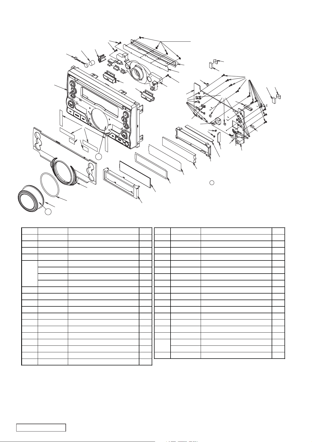
EXPLODED VIEW / PARTS LIST
Escutcheon section
13
7
12
6
5
4
3
A
2
17
1
A
14
15
18
Weld by heating
9
8
13
16
34
31X8
28
21
20
19
Note)1. Some parts depend on each model.
The model name is specified in the description.
11
10
32
26
33
27
26
25
30
34
29
24
23
22
A
: SANKOL application
Note) SANKOL uses CFD-409Z
13X11
35
31X8
10
11
NO. PART NO. DESCRIPTION Q'TY NO. PART NO. DESCRIPTION Q'TY
1 947-0785-00 KNOB ASSY 1 18 331-5080-00 LCD COVER
2 947-0784-00 DIAL ASSY 1 19 379-1457-51 INDICATOR(LCD)
3 347-8918-00 DOUBLE FACE 2 20 347-8922-00 BLACK FILM
4 347-8298-00 DOUBLE FACE 4 21 347-8921-00 WHITE FILM
5 940-8602-00 ES ASSY(PE-3402B-A) 1 22 335-9037-00 LCD ILLUMI
940-8602-08 ES ASSY(PE-3402B-B) 1 23 335-9038-00 LCD HOLDER
940-8602-02 ES ASSY(PE-3402K-A) 1 24 345-6526-00 RUBBER PART
940-8602-07 ES ASSY(PE-3402K-B) 1 25 074-4036-50 USB JACK(PE-3402B-A/K-B)
6 081-0040-00 MICRIPHONE 1 26 001-7088-92 DIODE
7 382-9582-00 BUTTON(RESET) 1 27 016-9900-94 VR W/SHAFT
8 346-0209-00 LEATHER SHEET 1 28 060-4021-00 IR-RECEIVER
9 371-3827-03 TRIM PLATE 1 29 075-9021-50 AUX JACK
10 345-5312-00 CUSHION 2 30 001-7062-90 DIODE
11 347-7321-00 E-SHEET 2 31 013-6312-50 TACT SWITCH
12 345-6422-00 SPONGE 1 32 076-0478-52 PLUG(2P)
13 716-0872-51 SPECIAL SCREW(M1.7x5) 14 33 074-3014-72 OUTLET SOCKET(22P)
14 382-9580-00 BUTTON(FW) 1 ------------ SWITCH PWB1
15 382-9579-00 BUTTON(FF) 1 ------------ SWITCH PWB2
16 335-9044-00 ILLUMI(MID) 1 35 076-0502-55 PLUG(5P)(PE-3402B-A/K-B)
17 347-8968-00 FILM 1
34
1
1
1
1
1
1
1
1
6
1
1
1
1
16
1
1
1
1
1
CX501/CX501B/CX501A
-8-
Page 9

Main section
33
34
34
33
35
32
1
34
28X6
1
34
28X4
8
13
7
1
3
12
11
10
44
24
39
30
2
31
40
20
34
4
23
4
22
29
27
4
32
3
1
26
19
18
1
16
1
2
17
35
14
45
15
33
42
31
36
30
43
2
5
37
1
1
4
21
1
2
3
NO. PART NO. DESCRIPTION Q'TY NO. PART NO. DESCRIPTION Q'TY
1 331-2869-00 SHIELD CASE 1 26 929-5110-80 CD-MECH-MODULE 1
2 074-2226-90 OUTLET SOCKET(40P) 2 27 310-1973-00 UPPER CASE 1
3 321-0969-00 CLAMP 1 28 345-3799-20 RUBBER PART 6
4 331-4794-00 TUNER BRKT 1 345-3799-20 RUBBER PART 4
5 076-0648-22 PLUG(22P) 2 29 313-2006-14 HEAT SINK 1
6 092-4000-51 ANT-RECEPT 1 30 716-1670-01 SCREW(M2X4) 3
7 075-0393-50 JACK 1 31 714-2603-8B MACHINE SCREW(M2.6x3) 4
8 331-45
9 331-3459-00 IC HOLDER 1 33 714-3006-8B MACHINE SCREW(M3x6) 5
10 051-2074-00 IC 1 34 731-3008-89 TAPTIGHT(M3X8) 9
11 009-9006-60 CHOKE 1 35 714-2610-8B MACHINE SCREW(M2.6x10) 4
12 331-4749-01 CONNECTOR HOLDER 1 36 731-2604-8H TAPTIGHT(M2.6X4) 2
13 074-1214-50 OUTLET SOCKET(16P) 1 37 276-0793-00 SETPLATE(PE-3402B-A) 1
14 331-5081-00 IC HOLDER 1 276-0861-00 SETPLATE(PE-3402B-B) 1
15 313-2039-03 HEAT SI
16 855-5562-51 RCA PIN CORD(6CH) 1 276-0860-00 SETPLATE(PE-3402K-B) 1
17 855-5585-50 RCA PIN CORD(4CH) 1 38 060-8105-50 ANT RECEPT 1
18 855-2508-50 SSP MINI DIN CORD 1 39 074-2215-65 OUTLET SOCKET(15P) 1
19 855-2507-50 HD MINI DIN CORD 1 40 074-2215-60 OUTLET SOCKET(10P) 1
20 335-0833-01 LEAD HOLDER 1 41 074-3014-72 OUTLET SOCKET(22P) 1
21 311-1859-08 LOWER CASE 1 42 ------------ MAIN PWB 1
22 854-4620-50 USB L
23 855-0642-50 USB CABLE 1 44 ------------ MECH PWB 1
24 816-3063-55 FLAT WIRE 1 45 051-3730-00 IC
25 331-4537-02 ES PLATE 1
PE-3402B-A
PE-3402B-B/K-A/K-B
PE-3402B-A/K-B
33-00 JACK HOLDER 1 32 714-2606-8B MACHINE SCREW(M2.6x6) 4
41
38
4
1
NK 1 276-0832-00 SETPLATE(PE-3402K-A) 1
EAD 1 43 ------------ BT PWB 1
25
PE-3402B-B/K-A
1
1
2
1
2
1
1
4
3
4
1
-9-
CX501/CX501B/CX501A
2
9
6
Page 10

ELECTRICAL PARTS LIST
p
p
p
p
p
p
p
p
p
p
(
)
p
p
p
p
p
p
p
p
p
p
Main PWB(B1) section
Note)1. Some parts depend on each model.
The model name is specified in the description.
REF No. PART No. DESCRIPTION REF No. PART No. DESCRIPTION REF No. PART No. DESCRIPTION
ANT201 092-4000-51
ANTENNA RECEPT
C101 187-1073-35 16V 100uF C215 168-1032-55 0.01uF K C421 043-1735-90 100
C214 168-1052-78 16V 1uF C420 187-2263-35 16V 22uF
FCH
C102 187-1073-35 16V 100uF C216 168-1032-55 0.01uF K C422 043-1735-90 100pF CH
C103 043-1735-90 100
F CH C217 168-1042-78 16V 0.1uF C423 043-1735-90 100pFCH
C104 043-1835-90 3900pF C218 168-2242-58 0.22uF B C424 043-1735-90 100pF CH
C105 043-1619-90 0.068uF C219 168-2232-55 0.022uF K C425 178-4742-78 0.47uF
C106 168-1022-55 1000pF K C220 177-1062-78 10pF C426 187-1053-65 50V 1uF
C107 043-1735-90 100
F CH C221 168-1042-78 16V 0.1uF C427 172-1041-11 0.1uF
C108 189-1083-32 16V 1000uF C222 168-1042-78 16V 0.1uF C428 042-1447-00 16V 2200uF
C109 043-1719-90 22
C110 043-1802-90 0.01uF C247 166-1201-50 12
F CH C223 166-1201-50 12pF CH D100 001-4301-41 HZU 7.5B2
F CH D101 001-1323-90 L1SS355T1G
C111 043-1719-90 22pF CH C249 168-1042-78 16V 0.1uF D106 001-1310-00 KDS160-RTK
C112 042-1577-00 6.3V 100uF C301 043-1838-90 4700
F D107 001-4301-26 HZU4.7B2
C113 168-1042-78 16V 0.1uF C302 043-1841-90 0.047uF D109 001-0466-61 1A4
C114 168-3332-78 0.033uF K C303 043-1838-90 4700
F D110 001-4301-26 HZU4.7B2
C115 168-1042-78 16V 0.1uF C304 187-1063-35 16V 10uF D111 001-0466-61 1A4
C116 187-1073-35 16V 100uF C305 187-1063-35 16V 10uF D112 001-1310-00 KDS160-RTK
C117 043-1802-90 0.01uF C308 187-1053-65 50V 1uF D113 001-1310-00 KDS160-RTK
C118 043-1802-90 0.01uF C309 187-1053-65 50V 1uF D121 001-0466-61 1A4
C119 043-1800-90 1000
F C310 187-1053-65 50V 1uF D160 001-1310-00 KDS160-RTK
C120 168-1032-55 0.01uF K C311 187-1053-65 50V 1uF D203 001-2630-90 1SS420-TPL3,F
C121 187-2253-65 50V 2.2uF C314 187-1063-35 16V 10uF D303 001-4316-17 LM3Z4V3T1G
C123 043-1804-90 0.1uF C315 187-1063-35 16V 10uF D401 001-4316-24 LM3Z8V2T1G
C124 187-2273-15 6.3V 220uF C316 187-1063-35 16V 10uF D403 001-1310-00 KDS160-RTK
C125 043-1735-90 100
F CH C317 187-1063-35 16V 10uF D404 001-1310-00 KDS160-RTK
C126 187-1063-35 16V 10uF C318 187-1063-35 16V 10uF D405 001-1310-00 KDS160-RTK
C127 187-2253-65 50V 2.2uF C319 187-1063-35 16V 10uF D406 001-0592-61 1N5404
C128 187-1063-35 16V 10uF C320 043-1804-90 0.1uF D601 001-0529-20 MA8039-L
C129 187-1053-65 50V 1uF C321 043-1804-90 0.1uF IC101 ----------------C130 043-1735-90 100pF CH C322 187-4763-15 6.3V 47uF
C131 043-1841-90 0.047uF C324 043-1723-90 33
F CH wrritten on
LC88F40HOPAU-QIP
(Software should be
C132 043-1804-90 0.1uF C325 043-1804-90 0.1uF production)
C133 187-1073-35 16V 100uF C326 043-1804-90 0.1uF
034900-052
C134 187-1073-35 16V 100uF C327 043-1804-90 0.1uF IC102 051-3218-90 TA76431F
C135 187-3363-45 25V 33uF C328 043-1804-90 0.1uF IC103 ----------------C136 187-1063-35 16V 10uF C329 187-1063-35 16V 10uF
C138 187-1063-35 16V 10uF C330 043-1804-90 0.1uF
C139 187-1063-35 16V 10uF C331 043-1800-90 1000pF
24LC256I-SN
(E2PROM Data
should be wrritten on
production)
C140 168-2242-58 0.22uF B C333 187-1063-35 16V 10uF (942990-051)
C141 043-1804-90 0.1uF C334 187-1063-35 16V 10uF IC104 051-5438-08 S-80830CN
C145 043-1802-90 0.01uF C335 187-1063-35 16V 10uF IC105 051-5437-58 R3111N211A
C147 187-1053-65 50V 1uF C336 043-1804-90 0.1uF IC106 051-3535-90 MM3144ANRE
C148 043-1804-90 0.1uF C337 043-1804-90 0.1uF IC107 051-3730-00 LV5680P
C149 043-1804-90 0.1uF C338 187-4763-35 16V 47uF IC108 051-3577-90
S-1206B33-U3TIG
C150 043-1804-90 0.1uF C339 043-1735-90 100pF CH IC201 051-4028-90 TEF6606
C151 165-1063-35 16V 10uF C340 043-1735-90 100pF CH IC301 051-3060-90 AZ4558M
C152 043-1804-90 0.1uF C341 187-1053-65 50V 1uF IC302 051-5048-90 NJW1222
C153 168-2242-58 0.22uF B C342 187-1053-65 50V 1uF IC303 051-3060-90 AZ4558M
C154 187-1063-35 16V 10uF C343 043-1735-90 100
C156 168-2242-58 0.22uF B C344 043-1735-90 100
C157 187-1063-35 16V 10uF C345 043-1735-90 100
C158 168-2242-58 0.22uF B C346 043-1735-90 100
F CH IC307 051-3059-90 NJM2120M
F CH IC402 051-2074-00 LV47017P
F CH J100 075-0393-50 3P
F CH J102 076-0648-22 22P
C159 168-2242-58 0.22uF B C360 043-1819-90 2200pF J105 074-2226-90 40P
C160 187-1063-35 16V 10uF C361 043-1819-90 2200
F J301 076-0648-22 22P
C161 168-2242-58 0.22uF B C364 043-1806-90 1pF J401 074-1214-50 16P
C162 165-1063-35 16V 10uF C365 043-1806-90 1
F L102 010-3100-66 2.2uH
C201 166-2096-50 2pF CK C366 043-1715-90 15pF CH L103 010-3100-66 2.2uH
C202 166-2201-50 22
C203 168-1022-55 1000
C204 168-1022-55 1000
F CH C367 043-1806-90 1pF L104 010-3100-66 2.2uH
F K C370 187-4763-15 6.3V 47uF L105 010-3407-59 5.6uH J
F K C371 187-1073-35 16V 100uF L106 010-3105-67
1.5k ohm/100kHz
C205 166-1201-50 12pF CH C372 187-2273-15 6.3V 220uF L201 010-2003-04 30uH
C206 168-1032-55 0.01uF K C409 178-4742-78 0.47uF L202 010-3406-50 1uH J
C207 168-1032-55 0.01uF K C410 178-4742-78 0.47uF L203 010-3406-53 1.8uH J
C208 168-1052-78 16V 1uF C411 178-4742-78 0.47uF L204 010-3406-43 0.27uH J
C209 168-2242-58 0.22uF B C412 178-4742-78 0.47uF L205 010-3062-54 LQH31HNR2
C210 166-1501-50 15
F CH C415 187-1063-35 16V 10uF L206 010-4054-00
#886ANS-0904QH
C211 166-3901-50 39pF CH C417 187-1063-35 16V 10uF L207 010-3072-90 560uH
C212 168-2242-58 0.22uF B C418 187-1063-35 16V 10uF L208 010-3072-90 560uH
C213 168-1042-78 16V 0.1uF C419 187-1063-35 16V 10uF L209 010-3105-62 1k ohm/100MHz
CX501/CX501B/CX501A
-10-
Page 11

REF No. PART No. DESCRIPTION REF No. PART No. DESCRIPTION REF No. PART No. DESCRIPTION
)
L210 010-3105-62
1k ohm/100MHz
R131 119-1031-15 1/10W 10k ohm R311 032-0140-89
L213 010-3407-58 4.7uH J R132 119-3321-15 1/10W 3.3k ohm R312 032-0140-89
L214 010-2198-87 82NH R133 032-0140-56
L302 010-3105-62
L303 010-3104-54
1k ohm/100MHz
600 ohm/100MHz
R134 119-2241-15
R135 032-0215-59
1/10W 12k ohm F
1/10W 220k ohm
1/10W 3.9k ohm(F)
R313 119-1021-15 1/10W 1k ohm
R314 119-1021-15 1/10W 1k ohm
R315 119-0000-05
Q101 125-9017-92 UMD3N-TR R136 119-1031-15 1/10W 10k ohm R316 032-0140-89
Q102 103-2394-00 2SD2394 R137 119-1041-15 1/10W 100k ohm R317 032-0140-89
1/10W 47k ohm F
1/10W 47k ohm F
1/10W 0 ohm JW
1/10W 47k ohm F
1/10W 47k ohm F
Q104 190-1576-00 2SA1576A R138 119-2241-15 1/10W 220k ohm R318 119-1031-15 1/10W 10k ohm
Q105 125-2027-92 DTC124EUA R139 119-5621-15 1/10W 5.6k ohm R319 119-1031-15 1/10W 10k ohm
Q106 125-3015-90 3CG1298 R14 119-1541-15 1/10W 150k ohm R320 119-1031-15 1/10W 10k ohm
Q109 125-2027-91 DTC114EUA R140 119-2231-15 1/10W 22k ohm R321 119-1031-15 1/10W 10k ohm
Q110 125-0021-92 DTA124EUA R141 032-0140-52
Q111 125-4024-90 3DG3875 R142 032-0215-58
Q112 125-2041-93 RT1N241M R143 032-0140-80
1/10W 33k ohm F
1/10W 24k ohm(F)
1/10W 18k ohm F
R322 032-0140-89
R323 119-5631-15 1/10W 56k ohm
R324 119-5631-15 1/10W 56k ohm
Q113 125-4024-90 3DG3875 R144 119-4731-15 1/10W 47k ohm R325 032-0140-89
1/10W 47k ohm F
1/10W 47k ohm F
Q114 190-1576-00 2SA1576A R145 116-1521-15 1/4W 1.5k ohm R326 119-3311-15 1/10W 330 ohm
Q115 131-1260-00 2SB1260 R146 119-4731-15 1/10W 47k ohm R327 119-5631-15 1/10W 56k ohm
Q116 125-2027-92 DTC124EUA R147 119-4731-15 1/10W 47k ohm R328 119-5631-15 1/10W 56k ohm
Q117 125-0021-95
DTA143ZUA-T106
R148 116-1521-15 1/4W 1.5k ohm R329 119-1011-15 1/10W 100 ohm
Q118 125-2027-92 DTC124EUA R149 116-4721-15 1/4W 4.7k ohm R330 119-1011-15 1/10W 100 ohm
Q119 125-0021-95
DTA143ZUA-T106
R150 119-1031-15 1/10W 10k ohm R331 119-1011-15 1/10W 100 ohm
Q120 190-1576-00 2SA1576A R151 119-6831-15 1/10W 68k ohm R332 119-1011-15 1/10W 100 ohm
Q122 125-2027-92 DTC124EUA R152 119-4721-15 1/10W 4.7k ohm R333 119-1011-15 1/10W 100 ohm
Q123 131-1260-00 2SB1260 R153 119-1031-15 1/10W 10k ohm R334 119-1011-15 1/10W 100 ohm
Q124 125-2041-93 RT1N241M R171 119-6831-15 1/10W 68k ohm R337 119-0000-05
Q401 198-3018-00 2SK3018 R172 119-4731-15 1/10W 47k ohm R338 119-0000-05
1/10W 0 ohm JW
1/10W 0 ohm JW
Q403 192-4081-00 2SC4081 R174 119-1021-15 1/10W 1k ohm R358 119-3311-15 1/10W 330 ohm
Q404 125-2027-95 DTC143ZU R181 119-0000-05
Q405 125-0021-95
DTA143ZUA-T106
R184 119-0000-05
1/10W 0 ohm JW
1/10W 0 ohm JW
R359 119-3311-15 1/10W 330 ohm
R363 119-1011-15 1/10W 100 ohm
Q406 125-2198-90 KRC110S R187 116-1521-15 1/4W 1.5k ohm R364 119-1021-15 1/10W 1k ohm
Q409 125-4012-90 KTD1304 R188 119-1031-15 1/10W 10k ohm R365 119-1021-15 1/10W 1k ohm
Q410 125-4012-90 KTD1304 R193 119-4721-15 1/10W 4.7k ohm R369 119-1031-15 1/10W 10k ohm
Q411 125-4012-90 KTD1304 R194 119-0000-05
Q412 125-4012-90 KTD1304 R195 119-0000-05
1/10W 0 ohm JW
1/10W 0 ohm JW
R370 119-1031-15 1/10W 10k ohm
R371 119-4731-15 1/10W 47k ohm
Q413 125-2027-95 DTC143ZU R196 119-4721-15 1/10W 4.7k ohm R375 119-2221-15 1/10W 2.2k ohm
Q417 192-4081-00 2SC4081 R197 119-1041-15 1/10W 100k ohm R378 119-1031-15 1/10W 10k ohm
R101 116-6811-15 1/4W 680 ohm R199 119-1031-15 1/10W 10k ohm R379 119-1031-15 1/10W 10k ohm
R102 116-6811-15 1/4W 680 ohm R200 119-1041-15 1/10W 100k ohm R404 119-4721-15 1/10W 4.7k ohm
R103 119-0000-05
1/10W 0 ohm JW
R201 119-4741-15 1/10W 470k ohm R406 119-1021-15 1/10W 1k ohm
R104 119-1031-15 1/10W 10k ohm R202 119-4741-15 1/10W 470k ohm R407 119-8221-15 1/10W 8.2k ohm
R105 119-1041-15
1/10W 100k ohm
R106 119-1031-15 1/10W 10k ohm R204 119-0000-05
R107 119-1811-15 1/10W 180 ohm R206 119-0000-05
R108 119-4721-15
1/10W 4.7k ohm
R203 119-1011-15 1/10W 100 ohm R408 119-1021-15 1/10W 1k ohm
R207 119-0000-05
1/10W 0 ohm JW
1/10W 0 ohm JW
1/10W 0 ohm JW
R409 119-2231-15 1/10W 22k ohm
R411 119-4711-15 1/10W 470 ohm
R412 119-1031-15 1/10W 10k ohm
R109 119-1811-15 1/10W 180 ohm R208 119-4721-15 1/10W 4.7k ohm R415 119-2231-15 1/10W 22k ohm
R110 119-1031-15 1/10W 10k ohm R209 116-2201-15 1/4W 22 ohm R416 119-2231-15 1/10W 22k ohm
R111 119-1031-15 1/10W 10k ohm R210 119-1011-15 1/10W 100 ohm R417 119-2231-15 1/10W 22k ohm
R112 119-2221-15
R113 032-0140-54
1/10W 2.2k ohm
1/10W 22k ohm F
R114 119-1031-15 1/10W 10k ohm R235 119-0000-05
R115 032-0140-54
R116 119-5641-15
R118 119-4721-15
1/10W 22k ohm F
1/10W 560k ohm
1/10W 4.7k ohm
R12 033-0000-05 1/10W 0 ohm R276 119-0000-05
R120 119-4731-15 1/10W 47k ohm R277 119-0000-05
R121 119-1031-15 1/10W 10k ohm R3 032-0140-70
R211 119-1011-15 1/10W 100 ohm R418 119-2231-15 1/10W 22k ohm
R229 119-0000-05
R272 119-0000-05
R274 119-0000-05
R275 119-0000-05
1/10W 0 ohm JW
1/10W 0 ohm JW
1/10W 0 ohm JW
1/10W 0 ohm JW
1/10W 0 ohm JW
1/10W 0 ohm JW
1/10W 0 ohm JW
1/10W 1.8k ohm F
R420 119-3311-15 1/10W 330 ohm
R421 119-3311-15 1/10W 330 ohm
R422 119-3311-15 1/10W 330 ohm
R424 119-3311-15 1/10W 330 ohm
R426 119-1021-15 1/10W 1k ohm
R427 119-1021-15 1/10W 1k ohm
R428 119-1031-15 1/10W 10k ohm
R429 116-4721-15 1/4W 4.7k ohm
R122 119-1031-15 1/10W 10k ohm R301 119-1041-15 1/10W 100k ohm R430 119-6831-15 1/10W 68k ohm
R123 119-1811-15 1/10W 180 ohm R302 119-1041-15 1/10W 100k ohm R431 119-1041-15 1/10W 100k ohm
R124 119-1031-15 1/10W 10k ohm R303 119-4721-15 1/10W 4.7k ohm R445 119-4731-15 1/10W 47k ohm
R126 119-2221-15
1/10W 2.2k ohm
R304 119-4721-15 1/10W 4.7k ohm SUP202 060-0122-20
DSP-141N-S00B
R127 119-1031-15 1/10W 10k ohm R305 119-1021-15 1/10W 1k ohm T401 009-9006-60 CHOKE 0.23mH
R128 119-2231-15 1/10W 22k ohm R306 119-1021-15 1/10W 1k ohm X101 061-1056-00 32.768kHz
R129 119-1031-15 1/10W 10k ohm R307 119-1021-15 1/10W 1k ohm X202 061-3031-00 4.00MHz
R13 119-5631-15 1/10W 56k ohm R308 032-0140-89
R130 119-1031-15 1/10W 10k ohm R309 032-0140-89
1/10W 47k ohm F
1/10W 47k ohm F
PWB 039-3740-00 PWB(WITHOUT
COMPONENT
The parts for PE-3402B-B/PE-3402K-A/B
REF No. PART No. DESCRIPTION REF No. PART No. DESCRIPTION REF No. PART No. DESCRIPTION
C248 187-1073-35 16V 100uF R176 119-0000-05 1/10W 0 ohm JW R185 119-1031-15 1/10W 10k ohm
R173 119-1031-15 1/10W 10k ohm R177 119-0000-05 1/10W 0 ohm JW R186 119-1031-15 1/10W 10k ohm
R175 119-0000-05
1/10W 0 ohm JW
R178 119-0000-05 1/10W 0 ohm JW R279 119-0000-05
-11-
1/10W 0 ohm JW
CX501/CX501B/CX501A
Page 12

The parts for PE-3402B-A
p
(
(
)
(
,
p
p
p
p
p
REF No. PART No. DESCRIPTION REF No. PART No. DESCRIPTION REF No. PART No. DESCRIPTION
C233 043-1608-90 0.1uF IC204 051-7538-90
SN74LVC3G17DCTR
R252 032-0140-63
C234 043-1841-90 0.047uF IC205 051-3060-90 AZ4558M R253 032-0140-63
C235 043-1841-90 0.047uF IC206 051-3060-90 AZ4558M R254 032-0140-89
C236 187-1063-35 16V 10uF IC304 051-3060-90 AZ4558M R255 032-0140-89
C237 187-1063-35 16V 10uF IC305 051-3060-90 AZ4558M R256 032-0140-63
C238 187-1063-35 16V 10uF IC306 051-3060-90 AZ4558M R257 032-0140-63
1/10W 27k ohm F
1/10W 27k ohm F
1/10W 47k ohm F
1/10W 47k ohm F
1/10W 27k ohm F
1/10W 27k ohm F
C239 187-1063-35 16V 10uF IC401 051-3605-90 NJM2360AM R258 119-1011-15 1/10W 100 ohm
C240 187-1063-35 16V 10uF L401 010-2285-56
C241 187-1063-35 16V 10uF L402 010-2285-56
2.25k ohm/100MHz
2.25k ohm/100MHz
R259 119-1011-15 1/10W 100 ohm
R261 119-4731-15 1/10W 47k ohm
C242 187-1063-35 16V 10uF L403 010-6003-03 270uH R262 119-1031-15 1/10W 10k ohm
C243 187-1063-35 16V 10uF L404 010-3406-66 22uH J R263 119-0000-05
1/10W 0 ohm JW
C244 189-1083-32 16V 1000uF Q201 125-2027-95 DTC143ZU R264 119-1031-15 1/10W 10k ohm
C245 165-1073-35 16V 100uF Q202 191-1197-50 2SB1197K Q
R R265 119-1031-15 1/10W 10k ohm
C306 187-1053-65 50V 1uF Q203 125-4024-90 3DG3875 R266 119-4721-15 1/10W 4.7k ohm
C307 187-1053-65 50V 1uF Q204 125-4024-90 3DG3875 R267 119-1531-15 1/10W 15k ohm
C312 187-1053-65 50V 1uF Q205 125-2027-92 DTC124EUA R268 119-1021-15 1/10W 1k ohm
C313 187-1053-65 50V 1uF Q206 125-3005-90 KTA1273 R270 116-1521-15 1/4W 1.5k ohm
C348 043-0540-00 6.3V 10uF Q407 125-4012-90 KTD1304 R271 116-1521-15 1/4W 1.5k ohm
C349 043-0540-00 6.3V 10uF Q408 125-4012-90 KTD1304 R281 119-1031-15 1/10W 10k ohm
C350 043-0540-00 6.3V 10uF R218 119-3321-15 1/10W 3.3k ohm R340 033-1041-15 1/10W 100k ohm
C351 043-0540-00 6.3V 10uF R219 119-1031-15 1/10W 10k ohm R341 033-1041-15 1/10W 100k ohm
C352 043-0540-00 6.3V 10uF R220 119-1821-15 1/10W 1.8k ohm R342 033-1041-15 1/10W 100k ohm
C353 043-0540-00 6.3V 10uF R221 119-4731-15 1/10W 47k ohm R343 033-1041-15 1/10W 100k ohm
C354 045-1011-50 100
C355 045-1011-50 100
C356 045-1011-50 100
C357 045-1011-50 100
F CH R224 119-1011-15 1/10W 100 ohm R344 033-1041-15 1/10W 100k ohm
F CH R225 119-1021-15 1/10W 1k ohm R345 033-1041-15 1/10W 100k ohm
F CH R226 119-1021-15 1/10W 1k ohm R346 033-1031-15 1/10W 10k ohm
F CH R227 119-1031-15 1/10W 10k ohm R347 033-1031-15 1/10W 10k ohm
C358 045-1011-50 100pF CH R228 119-1031-15 1/10W 10k ohm R348 033-1031-15 1/10W 10k ohm
C359 045-1011-50 100
F CH R230 119-0000-05
C401 042-1631-50 10V 100uF R231 119-0000-05
1/10W 0 ohm JW
1/10W 0 ohm JW
R349 033-1031-15 1/10W 10k ohm
R350 033-1031-15 1/10W 10k ohm
C402 168-1042-78 16V 0.1uF R234 119-6831-15 1/10W 68k ohm R351 033-1031-15 1/10W 10k ohm
C403 166-2211-50 220pF CH R236 119-1041-15
C404 168-2232-55 0.022uF K R237 119-1041-15
1/10W 100k ohm
1/10W 100k ohm
R352 033-1031-15 1/10W 10k ohm
R353 033-1031-15 1/10W 10k ohm
C405 187-1063-35 16V 10uF R238 119-1021-15 1/10W 1k ohm R354 033-1031-15 1/10W 10k ohm
C406 042-1452-81 10V 220uF R239 119-1041-15
1/10W 100k ohm
R355 033-1031-15 1/10W 10k ohm
C407 168-1042-78 16V 0.1uF R240 119-1021-15 1/10W 1k ohm R356 033-1031-15 1/10W 10k ohm
C408 042-1631-50 10V 100uF R241 119-1041-15
1/10W 100k ohm
R357 033-1031-15 1/10W 10k ohm
C414 187-1063-35 16V 10uF R242 032-0140-89 1/10W 47k ohm F R401 119-2291-15 1/10W 2.2 ohm
C416 187-1063-35 16V 10uF R243 032-0140-89 1/10W 47k ohm F R402 119-2291-15 1/10W 2.2 ohm
D200 001-4301-29 HZU 5.1B2 R244 032-0140-89 1/10W 47k ohm F R403 119-1531-15 1/10W 15k ohm
D201 001-4301-29 HZU 5.1B2 R245 032-0140-89 1/10W 47k ohm F R405 119-2721-15 1/10W 2.7k ohm
D202 001-1310-00 KDS160-RTK R246 032-0140-89 1/10W 47k ohm F R410 116-3911-15 1/4W 390 ohm
D301 001-4301-29 HZU 5.1B2 R247 032-0140-89 1/10W 47k ohm F R413 119-2231-15 1/10W 22k ohm
D304 001-4301-29 HZU 5.1B2 R248 032-0140-89 1/10W 47k ohm F R414 119-2231-15 1/10W 22k ohm
D402 001-2606-90 M1FS4 R249 032-0140-89 1/10W 47k ohm F R419 119-3311-15 1/10W 330 ohm
F301 060-0108-90
F302 060-8056-93
1/6ZP 0 ohm JW
CCP2E20HTTE
R250 032-0140-89 1/10W 47k ohm F R423 119-3311-15 1/10W 330 ohm
R251 032-0140-89 1/10W 47k ohm F R425 119-1021-15 1/10W 1k ohm
Switch PWB(B2) section
REF No. PART No. DESCRIPTION REF No. PART No. DESCRIPTION REF No. PART No. DESCRIPTION
C901 043-1802-90 0.01uF D914 001-7088-92 HSMF-A355- Q904 125-2027-95 DTC143ZU
C902 043-1804-90 0.1uF G33J1 Q905 193-1781-50 2SC3440
C903 043-1804-90 0.1uF D915 001-7088-92 HSMF-A355- Q906 193-1781-50 2SC3440
C904 043-1804-90 0.1uF G33J1 R903 119-4711-15 1/10W 470 ohm
C905 043-1804-90 0.1uF D916 001-7088-92 HSMF-A355- R904 119-2211-15 1/10W 220 ohm
C906 043-1804-90 0.1uF D918 001-2601-90 MA728 R905 119-1241-15 1/10W 120k ohm
C907 043-1804-90 0.1uF D919 001-1323-90 L1SS355T1G R906 119-4721-15 1/10W 4.7k ohm
C908 043-0603-90 16V 10uF D931 001-0584-21 MA8062 R907 119-1021-15 1/10W 1k ohm
C909 043-0603-90 16V 10uF D934 001-7062-90
C910 043-0603-90 16V 10uF IC901 051-6089-00 NJU6539 R910 119-1021-15 1/10W 1k ohm
C911 043-1808-90 1200pF IR901 060-4021-00 GPIUX51 R911 119-1041-15 1/10W 100k ohm
C912 043-1808-90 1200
F J702 075-9021-50 YW1310E431 R912 119-1031-15 1/10W 10k ohm
C914 043-1804-90 0.1uF J901 074-3014-72 22P R913 119-1031-15 1/10W 10k ohm
D909 001-4301-43 HZU8.2B1 J904 074-4036-50 4P
D910 001-4301-29 HZU5.1B2 /PE-3402K-B) R915 119-1011-15 1/10W 100 ohm
D911 001-7088-92 HSMF-A355- LCD901 379-1457-51
G33J1 LCD
D912 001-7088-92 HSMF-A355- P903 076-0478-52 2P R926 119-3311-15 1/10W 330 ohm
G33J1 P904 076-0502-55 5P
D913 001-7088-92 HSMF-A355- /PE-3402K-B) R928 119-3311-15 1/10W 330 ohm
G33J1 Q903 193-1781-50 2SC3440 R929 119-1031-15 1/10W 10k ohm
CX501/CX501B/CX501A
RBR1111C
R908 119-2711-15 1/10W 270 ohm
PE-3402B-A R914 119-3921-15 1/10W 3.9k ohm
INDICATOR R924 119-3311-15 1/10W 330 ohm
R925 119-1031-15 1/10W 10k ohm
PE-3402B-A R927 119-1031-15 1/10W 10k ohm
-12-
Page 13

REF No.PART No. DESCRIPTION REF No. PART No. DESCRIPTION REF No.PART No. DESCRIPTION
(
)
p
p
p
p
p
p
p
p
p
p
p
)
)
R936 119-1221-15 1/10W 1.2k ohm R954 119-1221-15 1/10W 1.2k ohm S902 013-6312-50 SWTICH
R937 119-1521-15 1/10W 1.5k ohm R955 119-1521-15 1/10W 1.5k ohm S903 013-6312-50 SWTICH
R938 119-1221-15 1/10W 1.2k ohm R956 119-1221-15 1/10W 1.2k ohm S920 013-6312-50 SWTICH
R939 119-1021-15 1/10W 1k ohm R957 119-1521-15 1/10W 1.5k ohm S922 013-6312-50 SWTICH
R940 119-1821-15 1/10W 1.8k ohm R958 119-1221-15 1/10W 1.2k ohm S923 013-6312-50 SWTICH
R941 119-1521-15 1/10W 1.5k ohm R959 119-1021-15 1/10W 1k ohm S924 013-6312-50 SWTICH
R942 119-1221-15 1/10W 1.2k ohm R960 119-1821-15 1/10W 1.8k ohm S926 013-6312-50 SWTICH
R943 119-1521-15 1/10W 1.5k ohm R961 119-1521-15 1/10W 1.5k ohm S927 013-6312-50 SWTICH
R944 119-1221-15 1/10W 1.2k ohm R962 119-1221-15 1/10W 1.2k ohm S928 013-6312-50 SWTICH
R945 119-1021-15 1/10W 1k ohm R963 119-1021-15 1/10W 1k ohm S930 013-6312-50 SWTICH
R946 119-1821-15 1/10W 1.8k ohm R964 119-1821-15 1/10W 1.8k ohm S931 013-6312-50 SWTICH
R947 119-1521-15 1/10W 1.5k ohm R965 119-1521-15 1/10W 1.5k ohm S932 013-6312-50 SWTICH
R948 119-1221-15 1/10W 1.2k ohm R966 119-1221-15 1/10W 1.2k ohm S936 013-6312-50 SWTICH
R949 119-1521-15 1/10W 1.5k ohm R967 119-1521-15 1/10W 1.5k ohm S938 013-6312-50 SWTICH
R950 119-1221-15 1/10W 1.2k ohm R968 119-1221-15 1/10W 1.2k ohm S939 013-6312-50 SWTICH
R951 119-1021-15 1/10W 1k ohm R969 119-1021-15 1/10W 1k ohm VR901 016-9900-94 VR W/SHAFT
R952 119-1821-15 1/10W 1.8k ohm R976 119-1821-15 1/10W 1.8k ohm PWB 039-3739-00 PWB
WITHOUT
R953 119-1521-15 1/10W 1.5k ohm R977 119-1521-15 1/10W 1.5k ohm COMPONENT
S901 013-6312-50 SWTICH
BT PWB (B3) section
REF No. PART No. DESCRIPTION REF No. PART No. DESCRIPTION REF No. PART No. DESCRIPTION
ANT601 060-8105-50 ANT-RECEPT C623 178-1052-78 1uF L606 010-3104-54 MPZ1608S601AT
C605 043-1735-90 100
C616 043-1804-90 0.1uF IC600 051-3577-90 S1206B33U- R619 119-1011-15 1/10W 100 ohm
C619 043-1715-90 15pF 3T1G PWB 039-3738-00 PWB(WITHOUT
C620 043-1715-90 15
C621 178-1052-78 1uF J600 074-3014-72 22P
C622 043-1804-90 0.1uF L604 010-3104-54
F C625 043-0603-90 10uF R618 119-1011-15 1/10W 100 ohm
F IC601 060-8123-90 GTBM501 COMPONENT
MPZ1608S601AT
REF No. PART No. DESCRIPTION REF No. PART No. DESCRIPTION REF No. PART No. DESCRIPTION
R547 033-4731-15
1/10W 47k ohm
R554 033-6801-15 1/16W 68 ohm R562 033-1531-15 1/10W 15k ohm
R548 033-0000-05 1/10W 0 ohm R555 033-6801-15 1/16W 68 ohm R563 033-1531-15 1/10W 15k ohm
R549 033-0000-05 1/10W 0 ohm R556 033-1041-15
R550 033-0000-05 1/10W 0 ohm R557 033-1041-15
R551 033-1031-15
R552 033-1031-15
1/10W 10k ohm
1/10W 10k ohm
R559 033-1031-15 1/10W 10k ohm X502 061-3580-90 12MHz
R560 033-1041-15
R553 033-4791-15 1/16W 4.7 ohm R561 033-1041-15
1/10W 100k ohm
1/10W 100k ohm
1/10W 100k ohm
1/10W 100k ohm
R564 033-0000-05 1/10W 0 ohm
X501 060-1535-90 16.934MHz
PWB 039-3737-00 PWB(WITHOUT
COMPONENT
PRINTED WIRING BOARD 1/5
CD PWB(B4) section
31
VCC
D-
D+
GND
F-GND
1
To Swith PWB(B2)(page 16)
Connect with Jump Wire
(PE-3402B-A/K-B)
COMPONENT SIDE
5
51
1
5
1
81
855-0642-50
(PE-3402B-B/K-A)
USB CABLE
CD PWB (B4) section
REF No. PART No. DESCRIPTION REF No. PART No. DESCRIPTION REF No. PART No. DESCRIPTION
C501 043-1608-90 0.1uF C540 043-1608-90 0.1uF R506 033-8231-15 1/10W 82k ohm
C502 165-1073-35 16V 100uF C541 043-1606-90 1000
C503 043-1608-90 0.1uF C542 043-1606-90 1000pF R508 033-1031-15 1/10W 10k ohm
C504 043-1608-90 0.1uF C543 043-0552-90 6.3V 47uF M R510 033-1031-15 1/10W 10k ohm
C505 042-0560-85 6.3V 100uF C544 043-1608-90 0.1uF R511 033-1031-15 1/10W 10k ohm
C506 043-1608-90 0.1uF C545 042-0560-85 6.3V 100uF R512 033-1031-15 1/10W 10k ohm
C507 043-1608-90 0.1uF C546 042-0560-85 6.3V 100uF R513 033-4711-15 1/10W 470 ohm
C508 043-1625-90 0.022uF C547 043-1706-90 5
C509 043-1824-90 0.22uF C548 043-1706-90 5
C510 043-1608-90 0.1uF C549 043-1608-90 0.1uF R516 033-6811-15 1/10W 680 ohm
C511 043-1806-90 1
F C550 043-1608-90 0.1uF R517 033-4731-15 1/10W 47k ohm
C512 043-1605-90 68pF C551 043-1608-90 0.1uF R518 033-6811-15 1/10W 680 ohm
C513 042-2273-25 10V 220uF M C552 043-1606-90 1000
C514 043-1606-90 1000pF C553 043-1608-90 0.1uF R520 033-4731-15 1/10W 47k ohm
C515 043-1608-90 0.1uF C554 165-4763-15 6.3V 47uF R521 033-1021-15 1/10W 1k ohm
C516 043-1608-90 0.1uF C555 043-1608-90 0.1uF R522 033-0000-05 1/10W 0 ohm
C517 042-0560-85 6.3V 100uF C556 043-1608-90 0.1uF R523 033-0000-05 1/10W 0 ohm
C518 043-1605-90 68
F C557 043-1608-90 0.1uF R524 033-1011-15 1/10W 100 ohm
C519 043-1607-90 0.01uF C558 042-0560-85 6.3V 100uF R525 033-2211-15 1/10W 220 ohm
C520 043-1608-90 0.1uF C560 043-1615-90 0.047uF R526 033-1011-15 1/10W 100 ohm
C521 042-0560-85 6.3V 100uF C561 043-1615-90 0.047uF R527 033-1041-15 1/10W 100k ohm
C522 043-1608-90 0.1uF C562 043-1614-90 470
C523 043-1607-90 0.01uF C563 043-1614-90 470pF R531 033-1031-15 1/10W 10k ohm
C525 043-1608-90 0.1uF D501 001-4326-50 RSB27F2T106 R532 033-6831-15 1/10W 68k ohm
C526 043-1615-90 0.047uF IC501 051-6101-90 BD8226EFV R533 033-1811-15 1/10W 180 ohm
C527 043-1607-90 0.01uF IC502 051-6934-90 MFI341S2313 R534 033-1011-15 1/10W 100 ohm
C528 043-1620-90 4700
F IC503 051-6754-00
C529 043-1608-90 0.1uF IC505 051-6926-90
C530 043-1615-90 0.047uF J501 074-2215-60 10P R537 033-0000-05 1/10W 0 ohm
C531 043-1625-90 0.022uF J502 074-2215-65 15P R538 033-0000-05 1/10W 0 ohm
C532 042-0560-85 6.3V 100uF J503 074-2226-90 40P R539 033-1231-15 1/10W 12k ohm
C533 043-0603-90 16V 10uF L501 010-3112-90 1k ohm/100MHz R540 033-0000-05 1/10W 0 ohm
C534 042-0560-85 6.3V 100uF L502 010-3112-90 1k ohm/100MHz R541 033-3321-15 1/10W 3.3k ohm
C535 043-0603-90 16V 10uF Q501 190-2060-00 2SA2060 R542 033-0000-05 1/10W 0 ohm
C536 043-1607-90 0.01uF R501 117-1821-15 1/8W 1.8k ohm R543 033-3311-15 1/10W 330 ohm
C537 043-1713-90 12
F R503 033-2731-15 1/10W 27k ohm R544 116-1501-15 1/4W 15 ohm
C538 043-1713-90 12pF R504 033-8231-15 1/10W 82k ohm R545 116-1501-15 1/4W 15 ohm
C539 043-1608-90 0.1uF R505 033-1241-15 1/10W 120k ohm R546 033-4701-15 1/10W 47 ohm
F R507 033-0000-05 1/10W 0 ohm
F R514 033-6831-15 1/10W 68k ohm
F R515 033-2231-15 1/10W 22k ohm
F R519 116-3391-15 1/4W 3.3 ohm
F R530 033-1031-15 1/10W 10k ohm
LC786960E-6AXX-L
BD2051AFJ-TR
R535 033-1811-15 1/10W 180 ohm
R536 033-0000-05 1/10W 0 ohm
Caution:
COMPONENT SIDE: Parts on the component
side seen from the component side are indicated.
SOLDER SIDE: Parts on the solder side seen
from the solder side are indicated.
1
13
To CD Mechanism
SOLDER SIDE
1
10
To PICK UP ASSY
15
140
USB
CONNECTOR
1
To J105 of Main PWB(B1) (page 14)
Connect with FLAT WIRE 816-3063-55
-13-
CX501/CX501B/CX501A
Page 14

PRINTED WIRING BOARD 2/5
Main PWB(B1) section 1/2
1
2
PE-3402B-A
PE-3402B-B/K-A/K-B
J
K
I
L
M
PON
OEM STEERING WHEEL
REMOTE CONTROL
INPUT JACK
16P Outlet Socket
P
H
1
855-5585-50
RCA PIN CODE
(4 CH)
OUT
LINE
2
RED
Gray
Purple
WHITE
RED
WHITE
FRONT/RIGHT
FRONT/LEFT
REAR/SUB WOOFER
RIGHT
REAR/SUB WOOFER
LEFT
LINE OUT
1
855-5562-51
RCA PIN CODE
(6 CH)
IJKLMNO
ABCDEFG
Gray
Black
Purple
RED
FRONT/RIGHT
FRONT/LEFT
WHITE
RED
REAR/RIGH
REAR/LEFT
WHITE
RED
SUB WOOFER/RIGH
SUB WOOFER/LEFT
WHITE
HD MINI DIN CORD
To HD tuner
855-2507-50
SSP MINI DIN CORD
To SIRIUS tuner
855-2508-50
Q IC
854-6487-50
EXTENAION LEAD
BROWN
GREEN/BLACK
GREEN
WHITE/BLACK
ABCDE FGH
BLUE
WHITE
GRAY
BLUE/WHITE
ORANGE/WHITE
GRAY/BLACK
PURPLE
RED
FUSE(15A) 120-0150-00
PURPLE/BLACK
YELLOW
BLACK
GND
IN
2
1
P
O
N
ML K J I
G
H
15
14
2
1
ABCDEF
SIRI-L
S-GND
HD-L
S-GND
HD-R
S-GND
SWR
FL
FR
S-GND
S-GND
RR/SWR
RL/SWL
SWL
2
TX
D-GND
POWER
RX
HE-DET
P-GND
1
SIRI-R
GND
17
RESET
TX
RX
B/U 14V
24
25
P-GND
1
17
EXTENSION-LEAD CONNECTOR
J401
Description
Port No.
A
SP R/L
SP F/L
B
SP F/L
C
SP F/R
D
E
SP F/R
F
SP R/R
SP R/R
G
B/U
H
I
SP R/L
PHONE INT
J
ACC
K
AUTO ANT BLUE
L
M
REMOTE
N
ILLUMI
NC
O
GND
P
LINE COLOR
GREEN
WHITE/BLACK
WHITE
GRAY
GRAY/BLACK
PURPLE
PURPLE/BLACK
YELLOW
GREEN/BLACK
BROWN
RED
BLUE/WHITE
ORANGE/WHITE
-------------
BLACK
COMPONENT SIDE
Caution:
COMPONENT SIDE: Parts on the component
side seen from the component side are indicated.
-14-
140
To J503 of CD PWB(B4) (page 13)
Connect with FLAT WIRE 816-3063-55
51
81
5
1
To J901 of Switch PWB(B2) (page 16)
CX501/CX501B/CX501A
1
1
31
1
1
1
1
5
5
2
5
1
1
2
1
2
1
22
21
22
21
To J600 of BT PWB(B3) (page 15)
Page 15

PRINTED WIRING BOARD 3/5
Main PWB(B1) section 2/2
1
2
The parts of a dotted line express the parts on a component side.
PE-3402B-A
PE-3402B-B/K-A/K-B
PRINTED WIRING BOARD 4/5
BT PWB(B3) section
SOLDER SIDE
Caution:
SOLDER SIDE: Parts on the solder side seen
from the solder side are indicated.
24
25
2
1
SOLDER SIDE
P
O
N
M
LKJI
A
BCDEF
1
G
H
1
21
15
14
2
1
22
To J301 of Main PWB(B1) (page 14)
1
2
2
2
COMPONENT SIDE
1
Caution:
22
21
2
1
22
21
2
1
COMPONENT SIDE: Parts on the component side seen from
the component side are indicated.
SOLDER SIDE: Parts on the solder side seen from the solder
side are indicated.
-15-
CX501/CX501B/CX501A
Page 16

PRINTED WIRING BOARD 5/5
Switch PWB(B2) section
The parts of a dotted line express the parts on a solder side.
Caution:
COMPONENT SIDE: Parts on the component side seen from the component side are indicated.
SOLDER SIDE: Parts on the solder side seen from the solder side are indicated.
CIRCUIT DIAGRAM 1/7
BT PWB(B3) section
[ ]
COMPONENT SIDE
SOLDER SIDE
Q IC
To J301 of Main PWB(B1)(page 19)
PE-3402B-A/K-B only
[4]
[5]
[6]
[RESET]
[ ]
PE-3402B-A/K-B only
[BAND]
VCC
D-
D+
GND
USB Connector
[ISR]
AUX INPUT JACK
To CD PWB(B4)(page 13)
Connect with Jump Wire
VCC
D-
D+
GND
VCC
DD+
GND
F-GND
26
22
21
51
[ROTARY]
1
76
2
1
To J102 of Main PWB(B1) (page 14)
[DISP]
[ ]
[SOUND]
[2]
[1]
[3]
[SOURCE]
-16-
[ ]
CX501/CX501B/CX501A
Page 17

CIRCUIT DIAGRAM 2/7
Main PWB(B1) section 1/4
1
1
2
PE-3402B-A
PE-3402B-B/K-A/K-B
To J503 of CD PWB(B4) (page 21)
Connect with FLAT WIRE 816-3063-55
1
1
2
2
1
To J901 of Switch PWB(B2) (page 22)
-17-
1
2
CX501/CX501B/CX501A
2
: To 2/4 (page 18)
3
: To 3/4 (page 19)
4
: To 4/4 (page 20)
Page 18

CIRCUIT DIAGRAM 3/7
Main PWB(B1) section 2/4
1
2
PE-3402B-A
PE-3402B-B/K-A/K-B
2
1
HD MINI DIN CORD
855-2507-50
To HD tuner
1
855-2508-50
SSP MINI DIN CORD
To SIRIUS tuner
-18-
CX501/CX501B/CX501A
: To 1/4 (page 17)
1
: To 3/4 (page 19)
3
4
: To 4/4 (page 20)
Page 19

CIRCUIT DIAGRAM 4/7
Main PWB(B1) section 3/4
1
2
PE-3402B-A
PE-3402B-B/K-A/K-B
1
PE-3402B-A only
2
1
PE-3402B-A only
To J600 of BT PWB(B3) (page 16)
-19-
CX501/CX501B/CX501A
1
: To 1/4 (page 17)
2
: To 2/4 (page 18)
4
: To 4/4 (page 20)
Page 20

CIRCUIT DIAGRAM 5/7
Main PWB(B1) section 4/4
1
2
PE-3402B-A
PE-3402B-B/K-A/K-B
1
1
OUT
LINE
855-5585-50
RCA PIN CODE
(4 CH)
2
OUT
LINE
855-5562-51
RCA PIN CODE
(6 CH)
1
-20-
CX501/CX501B/CX501A
IA
BACK
UP
P
H
1
: To 1/4 (page 17)
2
: To 2/4 (page 18)
3
: To 3/4 (page 19)
Page 21

CIRCUIT DIAGRAM 6/7
CD PWB(B4) section
To PICK UP-ASSY
To J105 of MAIN PWB(B1) (page 17)
Connect with FLAT WIRE 816-3063-55
To CD Mechanism
-21-
CX501/CX501B/CX501A
USB
CONNECTOR
USB CABLE
855-0642-50
(PE-3402B-B/K-A)
(PE-3402B-A/K-B)
To Switch PWB(B2)(page 22)
Connect with Jump Wire
Page 22

CIRCUIT DIAGRAM 7/7
Switch PWB(B2) section
[4]
[5]
[6]
[BAND] [ROTARY]
[DISP]
[ ]
[ISR]
AUX INPUT JACK
[1]
[ ]
[2]
[3]
[SOURCE]
To J102 of Main PWB(B1) (page 17)
ONLY FOR
PE-3402B-A/PE-3402K-B
[ ]
[ ]
[SOUND]
-22-
To CD PWB(B4)(page 21)
Connect with Jump Wire
CX501/CX501B/CX501A
Page 23

SERVICE MATERIAL
for PE-3402B-A / B-B / K-A / K-B
Page 24

Page 25

Page 26

Page 27

Page 28

Page 29

Page 30

Page 31

 Loading...