

EP7212
FEATURES
n ARM720T processor
— ARM7TDMI CPU
— 8 K-bytes of four-way set-associative cache
— MMU with 64-entry TLB (transition look-aside buffer)
—Write Buffer
—Windows
— Thumb code support enabled
Dynamically programmable clock speeds of
n
18, 36, 49, and 7 4 MHz at 2 .5 V
n Performance matching 100-MHz Intel
Pentium-based PC
n Ultra low power
— Designed for applications that require long battery life
while using standard AA/AAA batteries or rechargeable
cells
— Typical Power Numbers
● 90 mW at 74 MHz in the Operating State
● 30 mW at 18MHz in the Operating St a te
● 10 mW in the Idle State (clock to the CPU stopped,
everything else running)
● <1 mW in the S t andb y State (realtime clock ‘on’,
everything else stopped)
CE enabled
EP7212
High-Performance, Low-Power
System-on-Chip with LCD
Controller and Digital Audio
Interface (DAI)
OVERVIEW
The EP7212 is design ed f or ul t ra- lo w-p ower appl ica tions such as organizers / PDAs, two-way pagers,
smart cellular ph ones or any v ertical P DA device that
features t he ad d ed capability o f d ig ital audio decom pression. The co re-logic functionality of the device is
built around a n ARM720T processor with 8 K-bytes of
four-way set-associative unified cache and a write
buffer. Incorporated into the ARM720T is an
enhanced memory management unit (MMU) which
allows for suppor t of sophisti cated operat ing systems
like Microsoft Wi ndo ws CE.
(cont.) (cont.)
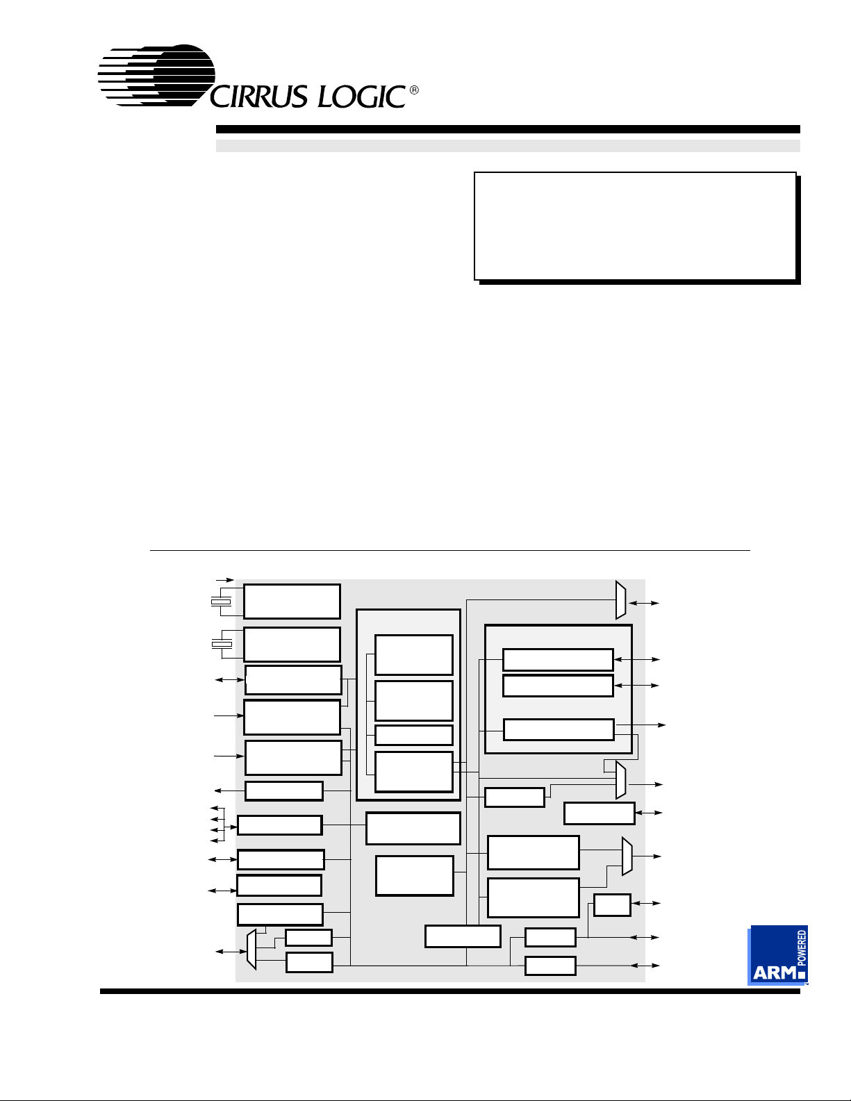
Functional Block Diagram
13-MHZ INPUT
3.6864 MHZ
32.768 KHZ
NPOR, RUN,
RESET, WAKEUP
BATOK, EXTPWR
PWRFL, BATCHG
EINT[1-3], FIQ,
MEDCHG
FLASHING LED DRIVE
PORTS A, B, D (8-BIT)
PORT E (3-BIT)
KEYBD DRIVERS (0-7)
BUZZER DRIVE
DC TO DC
ADCCLK, ADCIN,
ADCOUT, SMPCLK,
SSICLK, SSITXFR,
SSITXDA, SSIRXDA,
ADCCS
SSIRSFR
32.768-KHZ
OSCILLATOR
STATE CONTROL
POWER
MANAGEMENT
INTERRUPT
CONTROLLER
RTC
GPIO
PWM
SSI1 (ADC)
DAI
PLL
SSI2
CODEC
ARM720T
ARM7TDMI
CORE
CPU
8-KBYTE
CACHE
MMU
WRITE
BUFFER
TIMER
COUNTERS(2)
ON-CHIP
BOOT ROM
EPB BRIDGE
EPB BUS
INTERNAL DATA BUS
MEMORY CONTROLLER
CL-PS6700 INTF
EXPANSION CNTRL
DRAM CNTRL
INTERNAL ADDRESS BUS
LCD DMA
ICE-JTAG
LCD
CONTROLLER
ON-CHIP SRAM
38,400 BYTES
UART1
UART2
IrDA
D[0-31]
PB[0-1], NCS[4-5]
EXPCLK, WORD, NCS[0-3],
EXPRDY, WRITE
MOE, MWE,
RAS[0-1], CAS[0-3]
A[0-27],
DRA[0-12]
TEST AND
DEVELOPMENT
LCD DRIVE
LED AND
PHOTODIODE
ASYNC
INTERFACE 1
ASYNC
INTERFACE 2
Cirrus Logic, Inc. Copyright © Cirrus Logic, Inc. 20 00
P.O. Box 17847, Austin, Texas 78760 (All Rights Reserved)
(512) 445 7222 F AX: (512) 445 7851
http://www.cirrus.com
DS474PP1
FEB 00
1

Low-Power System-on-Chip with LCD Controller and Digital Audio Interface
FEATURES (cont.)
n Advanced audio decoder / decompression
capability
— Allows for support of multiple audio decompression
algorithms
— Supports MPEG 1, 2, & 2.5 layer 3 audio decoding,
including ISO compliant MPEG 1 & 2 layer 3 support for
all standard sample rates and bit rates
— Supports bit streams with adaptive bit rates
— DAI (Digital Audio Interface) providing glueless interface
to low-power DACs, ADCs, and Codecs
LCD controller
n
— Interfaces directly to a single-scan panel monochrome
LCD
— Panel width size is programmable from 32 to 1024 pixels
in 16-pixel increments
— Video frame buffer size programmable up to
128 kbytes
— Bits per pixel of 1, 2, or 4 bits
DRAM controller
n
— Supports both 16- and 32-bit-wide DRAMs
— EDO support (Fast Page Mode support for 13MHz and
18 MHz operation only)
Memory controller
n
— Decodes up to 6 separate memory segment s of up to
256 Mbytes each
— Each segment can be configured as 8, 16, or 32 bits
wide and supports page-mode access
— Programmable access time for conventional ROM /
SRAM / FLASH memory
— Supports Removable FLASH card interface
— Enables connection to removable FLASH card for
addition of expansion FLASH memory modules
n
38,400 bytes ( 0 x9 600) of on -ch i p S RAM for f as t
program execution and / or as a frame buffer
EP7212
n Synchronous serial interface
— ADC (SSI) Interface: Master mode only; SPI and
Microwire1
On-chip ROM; for manufacturing support
n
n 27-bits of general-purpose I/O
— Three 8-bit and one 3-bit GPIO port
— Supports scanning keyboard matrix
n
Two UARTs (16550 type)
— Supports bit rates up to 115 .2 kbps
— Contains two 16-byte FIFOs for TX and RX
— UART1 supports modem control signals
n
SIR (up to 115.2 kbps) infrared encoder / decoder
— IrDA (Infrared Data Association) SIR protocol encoder /
decoder
n DC-to-DC converter interface (PWM)
— Provides two 96-kHz clock outputs with programmable
duty ratio (from 1-in-16 to 15-in-16) that can be used to
drive a DC to DC converter
Two timer counters
n
n 208-pin LQFP or new 256-ball PBGA packages
n Evaluation kit available with BOM, schematics,
sample code, and design database
n Support for up to two ultra-low-power CL-PS6700
PC Card controllers
n Dedicated LED flasher pin from RTC
n Full JTAG boundary scan and Embedded ICE
support
n Commercial operating temperature range
-compatible (128 kbps operation)
OVERVIEW (cont.)
The EP7212 also includes a 32-bit Y2K-compliant
realtime clock and comp ar at or.
Power Management
The EP7212 is designed for ultra-low-power operation. Its core operates at only 2.5 V, while its I/O has
an operation range of 2.5 V–3.3 V. The device has
three basic power states:
Operating — This state is the full performance
state. All the clocks and peripheral logic are
enabled.
Idle — This state is the same as the Operating
St ate, exce pt th e CPU cl ock is halt ed wh ile w aiting for an event such as a key press.
2 DS474PP1
St andby — This state is equivalent to the computer
being switched off (no display), and the main
oscillator shut down. An event such as a key
press can wake-up the processor.
Memory Interfaces
There are two main ex te r nal memo r y in te rfa ces .
The first one i s the R OM / SRA M / FLASH- style int er-
face that has programm able wait-state timings and
includes burst-mode capability, with eight chip selects
decoding six 256-Mbyte sections of addressable
space. For maximu m flexibility, each bank can be
specified to be 8, 16, or 32 bits wide. This allows the
use of 8-bit-w ide boot ROM options t o minimize ov er-

EP7212
Low-Power System-on-Chip with LCD Controller and Digital Audio Interface
OVERVIEW (cont.)
all system cost. The on-chip boot ROM can be used
in product manuf acturing to se rially downlo ad system
code into system FLASH memory. To further minimize system memory requirements and cost, the
ARM Thumb
instruction se t is suppo rted, provi ding
for the use of high-speed 32-bit operations in 16-bit
op-codes and yiel ding industr y-leading co de density.
The second is the programmable 16- or 32-bit-wide
DRAM interface that allows direct conn ection of up to
two banks of DRAM, eac h ba nk co ntaining up to 256
Mbytes. To assure the lowest possible power consumption, the EP721 2 sup ports self-refresh DRAMs,
which are placed in a low-power state by the device
when it enters the low-power Standby State. EDO
and Fast Page DRAM are s upp or ted.
A DMA address generator is also provided that
fetches video disp lay dat a for the LCD controller f rom
main DRAM memory. The display frame buffer start
address is programmable. In addition, the built-in
LCD controller can utilize external or internal SRAM
for memory, thus eliminating th e nee d for DR AMs.
Digital Audio Capability
The EP7212 uses its powerful 3 2-bit RISC p rocessing engine to implement audio decompression algorithms in software. The nature of the on-board RISC
processor and the av ailabi lit y of e ff icien t C -compil ers
and other softwar e development t ools, ensures th at a
wide range of audio decompression algorithms can
easily be ported to and run on the EP7212.
Serial Interfaces
The EP7212 include s two 16550-type UARTs for RS232 serial communications, both of which have two
16-byte FIFOs for receiving and transmitting data.
The UARTs support bit rates up to 115.2 kbps. An
IrDA SIR protocol encoder / decoder can be optionally switched in to the RX / TX si gnals to / from one of
the UARTs to e nable these signals t o drive an infrared
communication interface directly.
Digital Audio Interface (DAI)
The EP7212 integrates an interface to enable a direct
connection to many low cost, low power, high quality
audio converters. In particular, the DAI can directly
interface with the Crystal
power audio DACs and the Cry stal
power ADC. Some of these devices feature digital
bass and treble boost, digital volume control and
compressor-limi ter fu ncti ons .
Packaging
The EP7212 is availabl e in a 208-pi n LQFP p ac kag e
and a 256-ball PBGA p a ckage.
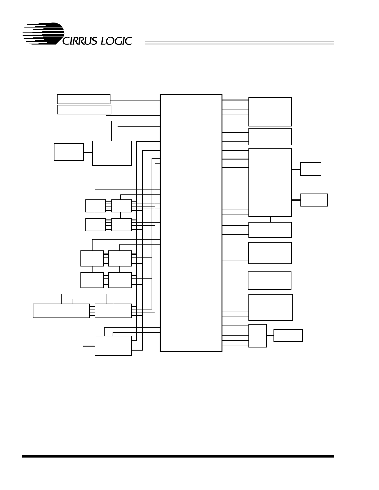
System Design
As shown in system block diagram, simply adding
desired memory and periphera ls to the highly
integrated EP7212 completes a low-power system
solution. All necessary interface logic is integrated
on-chip.
CS43L41 / 42 / 43 low-
CS53L32 low-
3DS474PP1
EP7212
Low-Power System-on-Chip with LCD Controller and Digital Audio Interface
CRYSTAL
CRYSTAL
PC CARD
SOCKET
EXTERNAL MEMORYMAPPED EXPANSION
ADDITIONAL I/O
CL-PS6700
PC CARD
CONTROLLER
× 16
DRAM
× 16
DRAM
× 16
FLASH
× 16
FLASH
BUFFERS
BUFFERS
LATCHES
DRAM
DRAM
× 16
FLASH
× 16
FLASH
AND
× 16
× 16
MOSCIN
RTCIN
CS[4]
PB0
EXPCLK
D[31:0]
A[27:0]
MOE
WRITE
RAS[1]
RAS[0]
CAS[0]
CAS[1]
CAS[2]
CAS[3]
NCS[0]
NCS[1]
CS[n]
WORD
CS[2]
CS[3]
DD[3:0]
COL[7:0]
PA[7:0]
PB[7:0]
PD[7:0]
PE[2:0]
PWRFL
BATOK
EXTPWR
BATCHG
EP7212
WAKEUP
DRIVE[1:0]
FB[1:0]
SSICLK
SSITXFR
SSITXDA
SSIRXDA
LEDDRV
PHDIN
RxD1/2
TxD1/2
ADCCLK
ADCCS
ADCOUT
ADCIN
SMPCLK
CL1
CL2
FM
POR
RUN
DSR
CTS
DCD
M
A EP7212–Based System
LCD MODULE
KEYBOARD
POWER
SUPPLY UNIT
AND
COMPARATORS
DC-TO-DC
CONVERTERS
CODEC/SSI2/
DAI
IR LED AND
PHOTODIODE
2× RS-232
TRANSCEIVERS
ADC
DIGITIZER
DC
INPUT
BATTERY
4 DS474PP1

EP7212
TABLE OF CONTENTS
1. CONVENTIONS ...................................................................................................................... 11
1.1 Acronyms and Abbreviations ............................................................................................ 11
1.2 Units of Measurement ......................................................................................................12
1.3 General Conventions ........................................................................................................12
1.4 Pin Description Conventions ............................................................................................. 12
2. PIN INFORMATION ..... ....... ...... ....... ...... ....... ...... ....... ...... ...... ................................................. 13
2.1 208-Pin LQFP Pin Diagram .............................................................................................. 13
2.2 Pin Descriptions ................................................................................................................ 14
2.2.1 External Signal Functions ................................................................................... 14
2.2.2 SSI/Codec/DAI Pin Multiplexing ............................................................................. 18
2.2.3 Output Bi-Directional Pins .................................................................................... 18
3. FUNCTIONAL DESCRIPTION ............................................................................................... 19
3.1 CPU Core .......................................................................................................................... 20
3.2 State Control ..................................................................................................................... 21
3.2.1 Standby State .......................................................................................................... 21
3.2.1.1 UART in Standby State ............................................................................... 22
3.2.2 Idle State ................................................................................................................. 23
3.2.3 Keyboard Interrupt ................................................................................................... 23
3.3 Power-Up Sequence ......................................................................................................... 23
3.4 Resets ............................................................................................................................... 24
3.5 Clocks ............................................................................................................................... 25
3.5.1 On-Chip PLL ............................................................................................................ 25
3.5.1.1 Characteristics of the PLL Interface ............................................................ 25
3.5.2 External Clock Input (13 MHz) ................................................................................ 26
3.5.3 Dynamic Clock Switching When in the PLL Clocking Mode .................................... 26
3.6 Interrupt Controller ............................................................................................................ 27
3.6.1 Interrupt Latencies in Different States ..................................................................... 27
3.6.1.1 Operating State ........................................................................................... 27
3.6.1.2 Idle State ..................................................................................................... 29
3.6.1.3 Standby State .............................................................................................. 29
3.7 EP7212 Boot ROM .......................................................................................................... 29
3.8 Memory and I/O Expansion Interface ............................................................................... 30
3.9 DRAM Controller with EDO Support ................................................................................. 31
3.10 CL-PS6700 PC Card Controller Interface ....................................................................... 33
3.11 Endianness ..................................................................................................................... 36
3.12 Internal UARTs (Two) and SIR Encoder ......................................................................... 36
3.13 Serial Interfaces .............................................................................................................. 38
EP7212
Contacting Cirrus Logic Support
For a complete listing of Direct Sales, Distributor, and Sales Representative contacts, visit the Cirrus Logic web site at:
http://www.cirrus.com/corporate/contacts/
Preliminary product in formati on descri bes pro ducts whic h are in pr oductio n, but for whi ch fu ll chara cteri zatio n data i s not yet avail able. Advance product information
describes products which are in devel opme nt and subject to development changes. Cirru s Logi c, I nc. has ma de best efforts to ensure that the infor mati on contained
in this document is accurate and rel i abl e. However, the information is sub j ect t o chan ge wi t hout notice and is provided “AS IS” with out warranty of any kind (express
or implied). No resp on s ibility is assumed by Cirrus Logic, Inc. fo r th e u s e of this information, nor for infringem ent s of patents or other rights of third parties. This doc
ument is the property of Cirrus Lo gic, I nc. and i mplies no li cense under paten ts, copyr ights, tradem arks, or t rade secrets. No part of t his pu blic ation m ay be copie d
reproduced, stored in a retrieval system, or transmitted, in any form or by any means (electronic, mechanical, photographic, or otherwise) without the prior written con
sent of Cirrus Logic, Inc. Items from any Cirrus Logic websit e or disk may be printed for use by the user . However, no part of the printout or electronic files may be
copied, reproduced, stored in a ret rieval system, or transmitted, i n any form or by any means (electronic, mech anical, photographi c, or otherwi se) without the prio
written consent of Cirrus Logic, Inc.Furthermore, no part of this publication may be used as a basis for manufacture or sale of any items without the prior written consen
of Cirrus Logic, Inc. T he names of produ cts of Cirrus L ogic, In c. or other ve ndor s and supp liers ap pear ing in this do cument may be t rademarks or service marks o
their respective owners which may be registered in some jurisdictions. A list of Cirrus Logic, Inc. trademarks and service marks can be found at http://www.cirrus.com
DS474PP1 5
DS474PP1

EP7212
3.13.1 Codec Sound Interface ..........................................................................................39
3.13.2 Digital Audio Interface ............................................................................................ 40
3.13.2.1 DAI Operation ............................................................................................41
3.13.2.2 DAI Frame Format ..................................................................................... 41
3.13.2.3 DAI Signals ................................................................................................42
3.13.3 ADC Interface — Master Mode Only SSI1 (Synchronous Serial Interface) ........... 42
3.13.4 Master / Slave SSI2 (Synchronous Serial Interface 2) ..........................................43
3.13.4.1 Read Back of Residual Data .....................................................................44
3.13.4.2 Support for Asymmetric Traffic .................................................................. 45
3.13.4.3 Continuous Data Transfer .........................................................................45
3.13.4.4 Discontinuous Clock .................................................................................. 45
3.13.4.5 Error Conditions ......................................................................................... 46
3.13.4.6 Clock Polarity ............................................................................................. 46
3.14 LCD Controller with Support for On-Chip Frame Buffer .................................................. 46
3.15 Timer Counters ...............................................................................................................47
3.15.1 Free Running Mode ...............................................................................................48
3.15.2 Prescale Mode ............................. ...... ....... ...... ...... ....................................... ....... ... 48
3.16 Real Time Clock .............................................................................................................. 49
3.16.1 Characteristics of the Real Time Clock Interface ...................................................49
3.17 Dedicated LED Flasher ................................................................................................... 49
3.18 Two PWM Interfaces .......................................................................................................49
3.19 Boundary Scan ................................................................................................................50
3.20 In-Circuit Emulation ......................................................................................................... 50
3.20.1 Introduction ..................................................... ...... ....... ...... ....... ...... .......................50
3.20.2 Functionality .................................................... ...... ....... ...... ....... ...... ....... ...... ....... ...51
3.21 Maximum EP7212-Based System ..................................................................................51
4. MEMORY MAP ...................................... ....... .......................................................................... 53
5. REGISTER DESCRIPTIONS .................................................................................................. 54
5.1 Internal Registers ..............................................................................................................54
5.1.1 PADR Port A Data Register .....................................................................................57
5.1.2 PBDR Port B Data Register .....................................................................................57
5.1.3 PDDR Port D Data Register ....................................................................................57
5.1.4 PADDR Port A Data Direction Register ...................................................................58
5.1.5 PBDDR Port B Data Direction Register ...................................................................58
5.1.6 PDDDR Port D Data Direction Register ...................................................................58
5.1.7 PEDR Port E Data Register .....................................................................................58
5.1.8 PEDDR Port E Data Direction Register ...................................................................58
5.2 SYSTEM Control Registers ...............................................................................................58
5.2.1 SYSCON1 The System Control Register 1 ............................................................. 58
5.2.2 SYSCON2 System Control Register 2 .....................................................................61
5.2.3 SYSCON3 System Control Register 3 .....................................................................63
5.2.4 SYSFLG1 — The System Status Flags Register .................................................... 64
5.2.5 SYSFLG2 System Status Register 2 .......................................................................66
5.3 Interrupt Registers .............................................................................................................67
5.3.1 INTSR1 Interrupt Status Register 1 .........................................................................67
5.3.2 INTMR1 Interrupt Mask Register 1 ..........................................................................68
5.3.3 INTSR2 Interrupt Status Register 2 .........................................................................69
5.3.4 INTMR2 Interrupt Mask Register 2 ..........................................................................69
5.3.5 INTSR3 Interrupt Status Register 3 .........................................................................70
5.3.6 INTMR3 Interrupt Mask Register 3 ..........................................................................70
5.4 Memory Configuration Registers .......................................................................................71
5.4.1 MEMCFG1 Memory Configuration Register 1 .........................................................71
5.4.2 MEMCFG2 Memory Configuration Register 2 .........................................................71
6 DS474PP1

EP7212
5.5 Timer / Counter Registers ................................................................................................. 74
5.5.1 TC1D Timer Counter 1 Data Register ..................................................................... 74
5.5.2 TC2D Timer Counter 2 Data Register ..................................................................... 74
5.5.3 RTCDR Real Time Clock Data Register ................................................................. 74
5.5.4 RTCMR Real Time Clock Match Register ............................................................... 74
5.6 LEDFLSH Register ...........................................................................................................75
5.7 PMPCON Pump Control Register ..................................................................................... 76
5.8 CODR — The CODEC Interface Data Register ................................................................ 77
5.9 UART Registers ................................................................................................................ 77
5.9.1 UARTDR1–2, UART1–2 Data Registers ................................................................. 77
5.9.2 UBRLCR1–2 UART1–2 Bit Rate and Line Control Registers ................................. 78
5.10 LCD Registers ................................................................................................................. 79
5.10.1 LCDCON — The LCD Control Register ................................................................ 79
5.10.2 PALLSW Least Signi fic an t Word — LCD Palette Register ................................... 80
5.10.3 PALMSW Most Significant Word — LCD Palette Register ................................... 81
5.10.4 FBADDR LCD Frame Buffer Start Address ........................................................... 81
5.11 SSI Register .................................................................................................................... 82
5.11.1 SYNCIO Synchronous Serial ADC Interface Data Register .................................. 82
5.12 STFCLR Clear all ‘Start Up Reason’ flags location ........ ....... ....................................... ... 83
5.13 End Of Interrupt Locations .............................................................................................. 83
5.13.1 BLEOI Battery Low End of Interrupt ...................................................................... 83
5.13.2 MCEOI Media Changed End of Interrupt .............................................................. 83
5.13.3 TEOI Tick End of Interrupt Location ...................................................................... 83
5.13.4 TC1EOI TC1 End of Interrupt Location ................................................................. 83
5.13.5 TC2EOI TC2 End of Interrupt Location ................................................................. 84
5.13.6 RTCEOI RTC Match End of Interrupt ....... ...... ...... ....................................... ....... ... 84
5.13.7 UMSEOI UART1 Modem Status Changed End of Interrupt .................................. 84
5.13.8 COEOI Codec End of Interrupt Location ............................................................... 84
5.13.9 KBDEOI Keyboard End of Interrupt Location ........................................................ 84
5.13.10 SRXEOF End of Interrupt Location ..................................................................... 84
5.14 State Control Registers ...................................................................................................84
5.14.1 STDBY Enter the Standby State Location ............................................................. 84
5.14.2 HALT Enter the Idle State Location ....................................................................... 84
5.15 SS2 Registers ................................................................................................................. 85
5.15.1 SS2DR Synchronous Serial Interface 2 Data Register ......................................... 85
5.15.2 SS2POP Synchronous Serial Interface 2 Pop Residual Byte ............................... 85
5.16 DAI Register Definitions ..................................................................................................85
5.16.1 DAIR DAI Control Register ... ....... ...... ....... ...... ....................................... ...... ....... ... 86
5.16.1.1 DAI Enable (DAIEN) .................................................................................. 87
5.16.1.2 DAI Interrupt Generation ........................................................................... 87
5.16.1.3 Left Channel Transmit FIFO Interrupt Mask (LCTM) ................................. 87
5.16.1.4 Left Channel Receive FIFO Interrupt Mask (LARM) ................................. 87
5.16.1.5 Right Channel Transmit FIFO Interrupt Mask (RCTM) .............................. 87
5.16.1.6 Right Channel Receive FIFO Interrupt Mask (RCRM) .............................. 88
5.16.1.7 Loopback Mode (LBM) .............................................................................. 88
5.16.2 DAI Data Registers .. ....... ...... ....... ...... ....... ...... ....................................... ...... ....... ... 89
5.16.2.1 DAIDR0 DAI Data Register 0 .......................... ...... ....... ............................. 89
5.16.2.2 DAIDR1 DAI Data Register 1 .......................... ...... ....... ............................. 90
5.16.2.3 DAIDR2 DAI Data Register 2 .......................... ...... ....... ............................. 91
5.16.3 DAISR DAI Status Register ................................................................................... 92
5.16.3.1 Right Channel Transmit FIFO Service Request Flag (RCTS) ................... 94
5.16.3.2 Right Channel Receive FIFO Service Request Flag (RCRS) ................... 94
5.16.3.3 Left Channel Transmit FIFO Service Request Flag (LCTS) ...................... 94
DS474PP1 7

EP7212
5.16.3.4 Left Channel Receive FIFO Service Request Flag (LCRS) ....................... 94
5.16.3.5 Right Channel Transmit FIFO Underrun Status (RCTU) ........................... 94
5.16.3.6 Right Channel Receive FIFO Overrun Status (RCRO) .............................94
5.16.3.7 Left Channel Transmit FIFO Underrun Status (LCTU) ..............................95
5.16.3.8 Left Channel Receive FIFO Overrun Status (LCRO) ................................95
5.16.3.9 Right Channel Transmit FIFO Not Full Flag (RCNF) .................................95
5.16.3.10 Right Channel Receive FIFO Not Empty Flag (RCNE) ........................... 95
5.16.3.11 Left Channel Transmit FIFO Not Full Flag (LCNF) ..................................95
5.16.3.12 Left Channel Receive FIFO Not Empty Flag (LCNE) ..............................95
5.16.3.13 FIFO Operation Completed Flag (FIFO) ..................................................95
6. ELECTRICAL SPECIFICATIONS .......................................................................................... 96
6.1 Absolute Maximum Ratings ..............................................................................................96
6.2 Recommended Operating Conditions ..............................................................................96
6.3 DC Characteristics ............................................................................................................ 96
6.4 AC Characteristics ............................................................................................................98
6.5 I/O Buffer Characteristics ................................................................................................ 110
6.6 JTAG Boundary Scan Signal Ordering ........................................................................... 111
7. TEST MODES ........ ...... ....................................... ....... ...... ...... ....... ...... ....... ...... ....... ...... ........114
7.1 Oscillator and PLL Bypass Mode .................................................................................... 114
7.2 Oscillator and PLL Test Mode ......................................................................................... 114
7.3 Debug / ICE Test Mode .................................................................................................. 115
7.4 Hi-Z (System) Test Mode ...............................................................................................115
7.5 Software Selectable Test Functionality ..........................................................................115
8. PIN INFORMATION ..... ....... ...... ....... ...... ....... ...... ....... ...... ............................................. ........116
8.1 208-Pin LQFP Pin Diagram .............................................................................................116
8.2 208-Pin LQFP Numeric Pin Listing ................................................................................. 117
8.3 256-Pin PBGA Pin Diagram ............................................................................................120
8.4 256-Ball PBGA Ball Listing ..............................................................................................121
9. PACKAGE SPECIFICATIONS .............................................................................................125
9.1 208-Pin LQFP Package Outline Drawing .......................................................................125
9.2 EP7212 256-Ball PBGA (17
10. ORDERING INFORMATION ............................................................................................... 127
11. APPENDIX A: BOOT CODE ..............................................................................................128
12. INDEX ................................................................................................................................. 133
× 17 × 1.53-mm Body) Dimensions ...................................126
8 DS474PP1

LIST OF FIGURES
Figure 1. 208-Pin LQFP (Low Profile Quad Flat Pack) Pin Diagram ............................................ 13
Figure 2. EP7212 Block Diagram..................................................................................................20
Figure 3. State Diagram................................................................................................................ 21
Figure 4. CLKEN Timing Entering the Standby State ................................................................... 26
Figure 5. CLKEN Timing Entering the Standby State ................................................................... 26
Figure 6. Codec Interrupt Timing .................................................................................................. 40
Figure 7. DAI Interface........................................................... ...... ....... .......................................... 41
Figure 8. EP7212 Rev C - Digital Audio Interface Timing – MSB / Left Justified format............... 42
Figure 9. SSI2 Port Directions in Slave and Master Mode............................................................ 44
Figure 10. Residual Byte Reading ................................................................................................45
Figure 11. Video Buffer Mapping .................................................................................................. 48
Figure 12. A Maximum EP7212 Based System............................................................................ 52
Figure 13. Consecutive Memory Read Cycles with Minimum Wait States ................................. 100
Figure 14. Sequential Page Mode Read Cycles with Minimum Wait States............................... 101
Figure 15. Consecutive Memory Write Cycles with Minimum Wait States.................................. 102
Figure 16. DRAM Read Cycles at 13 MHz and 18.432 MHz...................................................... 103
Figure 17. DRAM Read Cycles at 36 MHz.................................................................................. 104
Figure 18. DRAM Write Cycles at 13 MHz and 18 MHz ............................................................. 105
Figure 19. DRAM Write Cycles at 36 MHz.................................................................................. 106
Figure 20. Video Quad Word Read from DRAM at 13 MHz and 18 MHz ................................... 107
Figure 21. Quad Word Read from DRAM at 36 MHz.................................................................. 107
Figure 22. DRAM CAS Before RAS Refresh Cycle at 13 MHz and 18 MHz............................... 108
Figure 23. DRAM CAS Before RAS Refresh Cycle at 36 MHz................................................... 109
Figure 24. LCD Controller Timings.............................................................................................. 109
Figure 25. SSI Interface for AD7811/2........................................................................................ 110
Figure 26. SSI2 Interface Timings...............................................................................................110
Figure 27. 208-Pin LQFP (Low Profile Quad Flat Pack) Pin Diagram ........................................ 116
Figure 28. 256-Ball Plastic Ball Grid Array Diagram................................................................... 120
EP7212
LIST OF TABLES
Table 1. Acronyms and Abbreviations .......................................................................................... 11
Table 2. Unit of Measurement....................................................................................................... 12
Table 3. Pin Description Conventions........................................................................................... 12
Table 4. External Signal Functions ............................................................................................... 14
Table 5. SSI/Codec/DAI Pin Multiplexing...................................................................................... 18
Table 6. Output Bi-Directional Pins............................................................................................... 18
Table 7. Peripheral Status in Different Power Management States.............................................. 22
Table 8. Exception Priority Handling............................................................................................. 27
Table 9. Interrupt Allocation in the First Interrupt Register............................................................ 28
Table 10. Interrupt Allocation in the Second Interrupt Register .................................................... 28
Table 11. Interrupt Allocation in the Third Interrupt Register ........................................................ 28
Table 12. External Interrupt Source Latencies.............................................................................. 30
Table 13. Chip Select Address Ranges After Boot From On-Chip Boot ROM.............................. 30
Table 14. Boot Options ................................................................................................................. 31
Table 15. Physical to DRAM Address Mapping............................................................................ 32
Table 16. DRAM Address Mapping When Connected to an External 32-Bit DRAM
Memory System ............................................................................................................... 33
Table 17. CL-PS6700 Memory Map.............................................................................................. 34
Table 18. Space Field Decoding................................................................................................... 34
DS474PP1 9

EP7212
Table 19. Effect of Endianness on Read Operations .................................................................... 37
Table 20. Effect of Endianness on Write Operations ....................................................................37
Table 21. Serial Interface Options.................................................................................................39
Table 22. Serial-Pin Assignments................................................................................................. 39
Table 23. ADC Interface Operation Frequencies ..........................................................................43
Table 24. Instructions Supported in JTAG Mode ..........................................................................50
Table 25. Device ID Register ........................................................................................................51
Table 26. EP7212 Memory Map in External Boot Mode............................................................... 53
Table 27. EP7212 Internal Registers (Little Endian Mode)........................................................... 55
Table 28. EP7212 Internal Registers (Big Endian Mode)..............................................................57
Table 29. SYSCON1 ..................................................................................................................... 59
Table 30. SYSCON2 ..................................................................................................................... 61
Table 31. SYSCON3 ..................................................................................................................... 63
Table 32. SYSFLG ........................................................................................................................ 64
Table 33. SYSFLG2 ...................................................................................................................... 66
Table 34. INTSR1.......................................................................................................................... 67
Table 35. INSTR2..........................................................................................................................69
Table 36. INTSR3.......................................................................................................................... 70
Table 37. Values of the Bus Width Field ....................................................................................... 72
Table 38. Values of the Wait State Field at 13 MHz and 18 MHz .................................................72
Table 39. Values of the Wait State Field at 36 MHz......................................................................72
Table 40. MEMCFG ......................................................................................................................73
Table 41. LED Flash Rates ...........................................................................................................75
Table 42. LED Duty Ratio..............................................................................................................75
Table 43. PMPCON.......................................................................................................................76
Table 44. Sense of PWM control lines .......................................................................................... 76
Table 45. UARTDR1-2 UART1-2 ..................................................................................................77
Table 46. UBRLCR1-2 UART1-2 ..................................................................................................78
Table 47. LCDCON ....................................................................................................................... 79
Table 48. Grayscale Value to Color Mapping................................................................................81
Table 49. SYNCIO.........................................................................................................................82
Table 50. DAI Control Register .....................................................................................................86
Table 51. DAI Data Register 0 ......................................................................................................89
Table 52. DAI Data Register 1 ......................................................................................................90
Table 53. DAI Data Register 2 ......................................................................................................91
Table 54. DAI Control, Data and Status Register Locations .........................................................92
Table 55. absolute Maximum Ratings...........................................................................................96
Table 56. Recommended Operating Conditions ...........................................................................96
Table 57. DC Characteristics ........................................................................................................96
Table 58. AC Timing Characteristics.............................................................................................98
Table 59. Timing Characteristics................................................................................................... 99
Table 60. I/O Buffer Output Characteristics ................................................................................111
Table 61. 208-Pin LQFP Numeric Pin Listing.............................................................................. 111
Table 62. EP7212 Hardware Test Modes...................................................................................114
Table 63. Oscillator and PLL Test Mode Signals ........................................................................ 115
Table 64. Software Selectable Test Functionality ....................................................................... 115
Table 65. 208-Pin LQFP Numeric Pin Listing.............................................................................. 117
Table 66. 256-Ball PBGA Ball Listing..........................................................................................121
10 DS474PP1
EP7212
1. CONVENTIONS
This section presents acronyms, abbreviations,
units of measurement, and conventions used in this
data sheet.
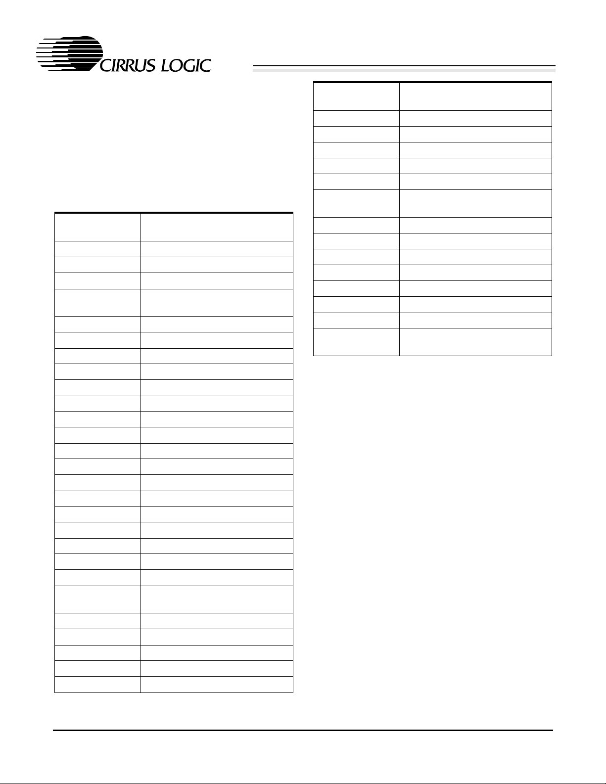
1.1 Acronyms and Abbreviations
Table 1 lists abbreviations and acronyms used in
this data sheet.
Acronym/
Abbreviation
AC alternating current.
A/D analog-to-digital.
ADC analog-to-digital co nve r ter.
CMOS
CODEC coder / decoder.
CPU central processing unit.
D/A digital-to-analog.
DC direct current.
DMA direct-memory access.
EPB embedded peripheral bus.
FCS frame check sequence.
FIFO first in / first out.
GPIO general purpose I/O.
ICT in circuit test.
IR infrared.
IrDA Infrared Data Association.
JTAG Joint Test Action Group.
LCD liquid crystal displa y.
LED light-emitting diode.
LQFP low profile quad flat pack.
LSB least significant bit.
MIPS
MMU memory management unit.
MSB most significant bit.
PBGA plastic ball grid array.
PCB printed circuit board.
PDA personal digital assistant.
complementary metal oxide
semiconductor.
millions of instructions per second.
Definition
Acronym/
Abbreviation
PIA peripheral inter face a dapt er.
PLL phase locked loop.
PSU power supply unit.
p/u pull-up resistor.
RAM random access memory.
RISC
ROM read-only memory.
RTC Real Time Clock.
SIR slow (9600–115.2 kb ps) infrared .
SRAM static random access memory.
SSI synchronous serial interface.
TAP te st ac ces s port.
TLB tran slati on loo ka side buffer.
UART
Table 1. Acronyms and Abbreviations (cont.)
reduced instruction set computer.
universal asynchro n ous
receiver.
Definition
Table 1. Acronyms and Abbreviations
DS474PP1 11
EP7212
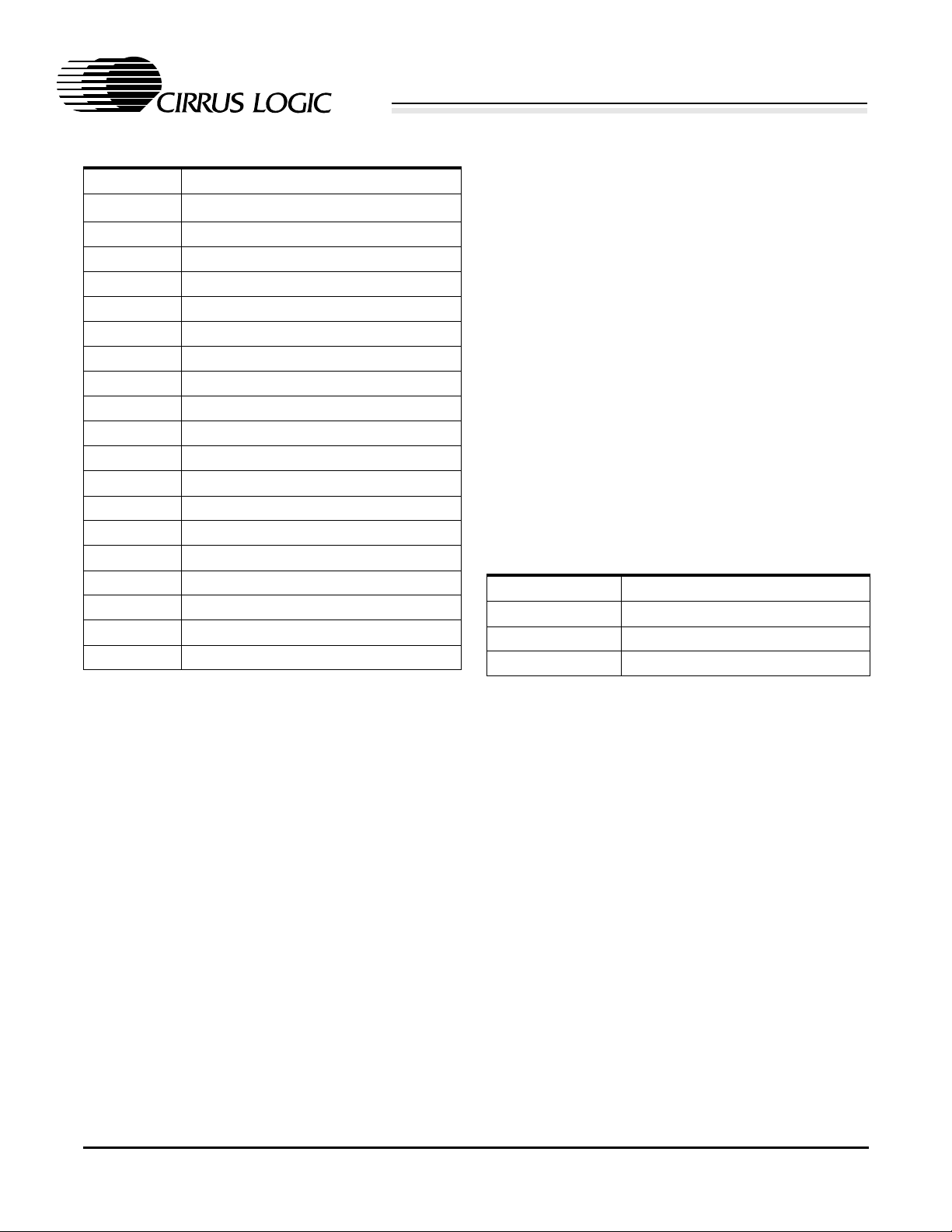
1.2 Units of Measurement
Symbol Unit of Measure
°C
Hz hertz (cycle per second)
kbits/s kilobits per second
kbyte kilobyte (1,024 bytes)
kHz kilohertz
Ω kilohm
k
Mbps megabits (1,048,576 bits) per second
Mbyte megabyte (1,048,576 bytes)
MHz megahertz (1,000 kilohertz)
µAmicroampere
µFmicrofarad
µWmicrowatt
µs microsecond (1,000 nanoseconds)
mA milliampere
mW milliwatt
ms millisecond (1,000 microseconds)
ns nanosecond
Vvolt
Wwatt
degree Celsius
a 0x at the beginning. For example, 0x14 and
03CAh are hexadecimal numbers. Binary numbers
are enclosed in single quotation marks when in text
(for example, ‘11’ designates a binary number).
Numbers not indicated by an ‘h’, 0x or quotation
marks are decimal.
Registers are referred to by acronym, as listed in
the tables on the previous page, with bits listed in
brackets MSB-to-LSB separated by a colon (:) (for
example, CODR[7:0]), or LSB-to-MSB separated
by a hyphen (for example, CODR[0–2]).
The use of ‘tbd’ indicates values that are ‘to be determined’, ‘n/a’ designates ‘not available’, and
‘n/c’ indicates a pin that is a ‘no connect’.
1.4 Pin Description Conventions
Abbreviations used for signal directions are listed
in Table 3.
Abbreviation Direction
I Input
OOutput
I/O Input or Output
Table 2. Unit of Measurement
1.3 General Conventions
Hexadecimal numbers are presented with all letters
in uppercase and a lowercase ‘h’ appended or with
Table 3. Pin Description Conventions
12 DS474PP1
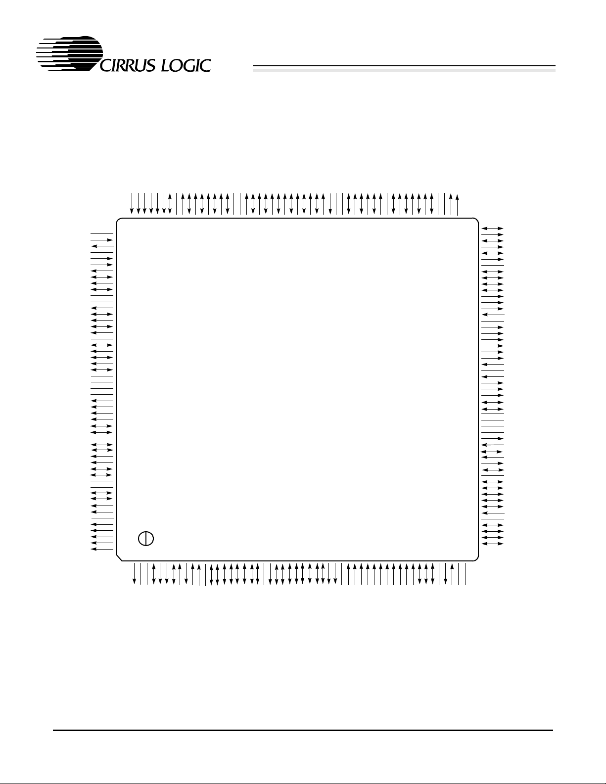
2. PIN INFORMATION
2.1 208-Pin LQFP Pin Diagram
EP7212
VDDOSC
MOSCIN
MOSCOUT
VSSOSC
WAKEUP
NPWRFL
A[6]
D[6]
A[5]
D[5]
VDDIO
VSSIO
A[4]
D[4]
A[3]
D[3]
A[2]
VSSIO
D[2]
A[1]
D[1]
A[0]
D[0]
VSSCORE
VDDCORE
VSSIO
VDDIO
CL[2]
CL[1]
FRM
DD[3]
DD[2]
VSSIO
DD[1]
DD[0]
NRAS[1]
NRAS[0]
NCAS[3]
NCAS[2]
VDDIO
VSSIO
NCAS[1]
NCAS[0]
NMWE
NMOE
VSSIO
NCS[0]
NCS[1]
NCS[2]
NCS[3]
NCS[4]
/DRA[10]
/DRA[12]
/DRA[11]
NEXTPWR
BATOK
NPOR
NURESET
NMEDCHG/NBROM
156
155
157
158
159
160
161
162
163
164
165
166
167
168
169
170
171
172
173
174
175
176
177
178
179
180
181
182
183
184
185
186
M
187
188
189
190
191
192
193
194
195
196
197
198
199
200
201
202
203
204
205
206
207
208
1
D[7]
A[7]
D[8]
A[8]
D[9]
D[10]
A[10]
VSSIO
VDDIO
A[11]
D[12]
A[12]
D[13]
A[13]
D[14]
NBATCHG
VSSIO
154
153
152
151
150
149
148
147
146
D[11]
A[9]
145
144
143
140
139
138
137
141
142
A[14]
132
134
136
135
133
D[17]
D[15]
131
A[15]
130
A[17]
NTRST
A[16]
128
VSSIO
124
125
126
127
D[16]
129
EP7212
208-Pin LQFP
(Top View)
2345678910111213141516171819202122232425262728293031323334353637383940414243444546474849515052
VDDIO
D[18]
122
123
/DRA[8]
/DRA[9]
A[18
D[19]
A[19]
119
120
121
/DRA[6]
/DRA[4]
A[23]
110
/DRA[3]
D[24]
VSSIO
VDDIO
A[24]
HALFWORD
106
107
108
109
105
104
103
102
101
100
99
98
97
96
95
94
93
92
91
90
89
88
87
86
85
84
83
82
81
80
79
78
77
76
75
74
73
72
71
70
69
68
67
66
65
64
63
62
61
60
59
58
57
56
55
54
53
D[25]
A[25]/DRA[2 ]
D[26]
A[26]/DRA[1 ]
D[27]
A[27]/DRA[0 ]
VSSIO
D[28]
D[29]
D[30]
D[31]
BUZ
COL[0]
COL[1]
TCLK
VDDIO
COL[2]
COL[3]
COL[4]
COL[5]
COL[6]
COL[7]
FB[0]
VSSIO
FB[1]
SMPCLK
ADCOUT
ADCCLK
DRIVE[0]
DRIVE[1]
VDDIO
VSSIO
VDDCORE
VSSCORE
NADCCS
ADCIN
SSIRXFR
SSIRXDA
SSITXDA
SSITXFR
VSSIO
SSICLK
PD[0]/LEDFL SH
PD[1]
PD[2]
PD[3]
TMS
VDDIO
PD[4]
PD[5]
PD[6]
PD[7]
/DRA[7]
D[20]
A[20]
117
118
/DRA[5]
VSSIO
A[21]
D[22]
D[23]
A[22]
D[21]
111
112
113
114
115
116
TDI
PB[7]
PB[6]
PB[5]
PB[4]
VSSIO
VDDIO
NCS[5]
EXPCLK
TXD[2]
WORD
WRITE
VSSIO
RXD[2]
EXPRDY
PB[3]
RUN/CLKEN
TDO
PB[2]
PB[1]/PRDY[2]
PB[0]/PRDY[1]
VDDIO
PA[6]
PA[5]
PA[4]
PA[3]
PA[2]
PA[1]
PA[7]
PA[0]
TXD[1]
LEDDRV
CTS
DSR
DCD
VSSIO
PHDIN
RXD[1]
EINT[3]
NEINT[2]
NEINT[1]
NTEST[1]
NEXTFIQ
NTEST[0]
PE[2]/CLKSEL
PE[1]BOOTSEL[1]
PE[0]BOOTSEL[0]
N/C
RTCIN
VDDRTC
VSSRTC
RTCOUT
Notes: 1) For package specifications, please see 208--Pin LQFP Package Outline Drawing on page 125
2) N/C should not be grounded but left as no connects
Figure 1. 208-Pin LQFP (Low Profile Quad Flat Pack) Pin Diagram
DS474PP1 13
EP7212
2.2 Pin Descriptions
Table 4 describes the function of all the external signals to the EP7212. Note that all output signals and all
I/O pins (when acting as outputs) are three stateable. This is to enable the Hi-Z test modes to be supported.
2.2.1 External Signal Functions
Function Signal
Signal Description
Name
Data bus D[0-31] I/O 32-bit system data bus for memory, DRAM, and I/O interface
A[0-14] O 15 bits of system byte address during memory and expansion cycles
Address bus
Memory
Interface
A[15-27]
DRA[0-12]
nRAS[0-1] O Row Address Select outputs to DRAM banks 0 to 1.
nCAS[0-3] I/O Column Address Select outputs allowing for bytes 0 to 3 within a 32-bit word.
nMOE O Memory output enable
nMWE O Memory write enable
nCS[0-3] O Chip select; active low, SRAM-like chip selects for expansion
nCS[4-5] O Chip select; active low, CS for expansion or for CL-PS6700 select
EXPRDY I Expansion port ready; external expansion devices drive this low to extend the
WRITE O Write strobe, low during reads, high during writes from the EP7212
WORD/
HALFWORD
DRA[0-12] is multiplexed with A[15-27], offering additional power savings
since the lightest loading is exp ect ed on the hig h or der ROM addres s lines .
Whenever the EP7212 is in the Standby State, the external address and data
buses are driven low. The RUN signal is used internally to force these buses to
be driven low. This is done to p reve nt perip herals that are powe red-d own from
draining current. Also, the internal peripheral’s signals get set to their Reset
State.
bus cycle. This is used to insert wait states for an external bus cycle.
O To do write accesses of dif ferent s izes W ord and Half -W ord must be externall y
decoded. The encoding of these signals is as follows:
Access Size Word Half-Word
Word 1 0
Half-Word * 1
Byte 0 0
The core will generate an address. When doing a read, the ARM core will
select the appropriate byte channels. When doing a write, the correct bytes
will have to be enabled depending on the above signals and the least significant bits of the address bus.
The ARM architecture does no t sup port un ali gne d ac ces s es. For a read using
x 32 memory, it is assumed tha t y ou w ill i gno re b it s 1 an d 0 of the address bus
and perform a word rea d (or i n po wer c ritical systems decode the relevant bits
depending on the size of the access). If an unaligned read takes place, the
core will rotate the resulting data in the register. For more information on this
behavior see the LDR instruction in the ARM7TDMI data sheet.
EXPCLK I/O Expansion clock rate is the same as the CP U cl ock fo r 13MHz and 18 MHz. It
runs at 36.864 MHz for 36,49 and 74 MHz modes; in 13 MHz mode this pin is
used as the clock input.
Table 4. External Signal Functions
14 DS474PP1

EP7212
Function Signal
Name
nMEDCHG/
nBROM
Interrupts
Power
Management
State Control
nEXTFIQ I External active low fast interrupt request input
EINT[3] I External active high interrupt request input
nEINT[1:2] I Two general purpose, active low interrupt inputs
nPWRFL
BATOK
nEXTPWR I External power sense; must be driven low if the system is powered by an
nBATCHG
nPOR I Power-on reset input. This signal is not deglitched. When active it completely
RUN/CLKEN I/O This pin is programmed to either output the RUN signal or the CLKEN signal.
WAKEUP
nURESET
Signal Description
I Media changed input; active low, deglitched. Used as a general purpose FIQ
interrupt during normal ope r ati on. It is also us ed on pow er up to co nfi gure the
processor to either boot from the internal Boot ROM, or from external memory.
When low, the chip will boot from the internal Boot ROM.
1
1
1
1
I Power fail input; active low, deglitched input to force system into the Standby
State
I Main battery OK in put; fallin g edge generat es a FIQ , a low level i n the Standby
State inhibits system start up; deglitched input
external source
I New battery sense; driven low if battery voltage falls below the "no-battery"
threshold; it is a deglitched input
resets the entire system, including all the RTC registers. Upon power-up, the
signal must be held active low for a minimum of 100 µsec after V
tled. During normal operation, nPOR needs to be held low for at least one
clock cycle of the selected clock speed (i.e., when running at 13 MHz, the
pulse width of nPOR needs to be > 77 nsec).
Note that nURESET, RUN/CLKEN, TEST(0), TEST(1), PE(0), PE(1), PE(2),
DRIVE(0), DRIVE(1), DD(0), DD(1), DD(2), and DD(3) are all latched on the
rising edge of nPOR.
The CLKENSL bit is used to configure this pin. When RUN is selected, the pin
will be high when the system is active or idle, low while in the Standby State.
When CLKEN is selected, the pin will only be driven low when in the Standby
State (For RUN, see Table 6).
I
Wake up is a deglitched input signal. It must also be held high for at
least 125
µsec to guarantee its detection. Once detected it forces the
system into the Operating State from the Standby State. It is only
active when the system is in the Standby State. This pin is ignored
when the system is in the Idle or Operating State. It is used to wakeup
the system after first power-up, or after software has forced the system
into the Standby State. WAKEUP will be ignored for up to two seconds
after nPOR goes HIGH. Therefore, the external WAKEUP logic must
be designed to allow it to rise and stay HIGH for at least 125 usec, two
seconds after nPOR goes HIGH.
1
I User reset input; active low deglitched input from user reset button.
This pin is also latched upon the rising edge of nPOR and read along with the
input pins nTEST[0-1] to force the device into special test modes. nURESET
does not reset the RTC.
has set-
DD
Table 4. External Signal Functions (cont.)
DS474PP1 15

EP7212
Function Signal
DAI, Codec or
SSI2
Interface
(See Table 5 for
pin assignment
and direction following multiplex-
ing)
ADC
Interface
(SSI1)
IrDA and
RS232
Interfaces
LCD
Keyboard &
Buzzer drive
LED Flasher
SSITXFR I/O DAI/Codec/SSI2 serial data output frame/synchronization pulse output
SSITXDA O DAI/Codec/SSI2 serial data output
SSIRXDA I DAI/Codec/SSI 2 serial data input
SSIRXFR I/O SSI2 serial data i nput frame/synchronization pulse
ADCOUT O Seria l data output
SMPCLK O Sample clock output
RXD[1-2] I RS232 UART1 and 2 RX inputs
LEDFLSH
Signal Description
Name
SSICLK I/O DAI/Codec/SSI2 clock signal
DAI external clock input
ADCCLK O Serial clock output
nADCCS O Chip select for ADC interface
ADCIN I Serial data input
LEDDRV O Infrared LED drive output (UART1)
PHDIN I Photo diode input (UART1)
TXD[1-2] O RS232 UART1 and 2 TX outputs
DSR I RS232 DSR input
DCD I RS232 DCD input
CTS I RS232 CTS input
DD[0-3] I/O LCD serial display data; pins can be used on power up to read the ID of some
LCD modules (See Table 6).
CL[1] O LCD line clock
CL[2] O LCD pixel clock
FRM O LCD frame synchronization pulse output
M O LCD AC bias drive
COL[0-7] O Keyboard column drives (SYSCON1)
BUZ O Buzzer drive output (SYSCON1)
PD[0]/
O LED flasher driver — multiplexed with Port D bit 0. This pin can provide up to
4 mA of drive current.
Table 4. External Signal Functions (cont.)
16 DS474PP1

EP7212
Function Signal
Signal Description
Name
PA[0:7] I/O Port A I/O (bit 6 for boot clock option, bit 7 for CL-PS6700 PRDY input); also
used as keyboard row inputs
General
Purpose I/O
PWM
Drives
Boundary
Scan
Test nTEST[0:1] I Test mode select inputs . Thes e pins are u sed in conju nct ion with t he pow er-on
Oscillators
No Connects N/C No connects should be left as no connects; do not connect to ground
PB[0]/PRDY1
PB[1]/PRDY2
PB[2:7]
PD[0:7] I/O Port D I/O
PE[0]/
BOOTSEL[0]
PE[1]/
BOOTSEL[1]
PE[2]/
CLKSEL
DRIVE[0:1] I/O PWM drive outputs. These pins are inputs on power up to determine w hat
FB[0:1] I PWM feedback inputs
TDI I JTAG data in
TDO O JTAG data out
TMS I JTAG mode select
TCLK I JTAG clock
nTRST I JTAG async reset
MOSCIN
MOSCOUT
RTCIN
RTCOUT
I/O Port B I/O. All eight Port B bits can be used as GPIOs.
When the PC CARD1 or 2 control bits in the SYSCON2 register are deasserted, PB[0] and PB[1] are available for GPIO. When asserted, these port
bits are used as the PRDY signals for connected CL-PS6700 PC Card Host
Adapter devices.
I/O Port E I/O (3 bits only). Can be used as general purpose I/O during normal
operation.
I/O During power-on reset, PE[0] and PE[1] are inputs and are latched by the ris-
ing edge of nPOR to s el ect the me mo ry wi d th tha t th e EP7212 will use to read
from the boot code storage device (i.e., external 8-bit-wide FLASH bank).
I/O During power-on reset, PE[2] is latched by the rising edge of nPOR to select
the clock mode of operation (i.e., either the PLL or external 13 MHz clock
mode).
polarity the output of the PWM should be when active. Otherwise, these pins
are always an output (See Table 6).
latched state of nURESET to select between the various device test models.
I
Main 3.6864 MHz oscillator for 18.432 MHz–73.728 MHz PLL
O
I
Real Time Clock 32.768 kHz oscillator
O
Table 4. External Signal Functions (cont.)
1. All deglitched inputs are via the 16.384 kHz clock. Each deglitched signal must be held active for at least two clock periods. Therefore, the
input signal must be active for at least ~125
µs to be detected cleanly.
The RTC crystal must be populated for the device to function properly.
DS474PP1 17
EP7212
2.2.2 SSI/Codec/DAI Pin Multiplexing
SSI2 Codec DAI Direction Strength
SSICLK PCMCLK SCLK I/O 1
SSITXFR PCMSYNC LRCK I/O 1
SSITXDA PCMOUT SDOUT Output 1
SSIRXDA PCMIN SDIN Input
SSIRXFR p/u* MCLK I/O 1
* p/u = use an ~10 k pull-up
The selection between SSI2 and the codec is controlled by the state of the SERSEL bit in SYSCON2 (See
SYSCON2 System Control Register 2). The choice between the SSI2, codec, and the DAI is controlled by
the DAISEL bit in SYSCON3 (See SYSCON3 System Control Register 3).
Table 5. SSI/Codec/DAI Pin Mu lt iplexing
2.2.3 Output Bi-Directional Pins
RUN The RUN pin is looped back in to skew the address and data bus from each other.
nCAS[3:0] The nCAS pins are looped back into the EP7212 to be used as the actual clock source for the data to be
latched internally.
Drive [0-1] Drive 0 and 1 are looped back in on power up to determine what polarity the output of the PWM should be
when active.
DD[3:0] DD[3:0] are looped back in on power up to enable the reading of the ID of some LCD modules.
NOTE: The above output p ins are implemen ted as b i-direction al pins to enable the output side of the pad to
be monitored and hence provide more accurate control of timing or duration.
Table 6. Output Bi-Directional Pin s
18 DS474PP1

EP7212
3. FUNCTIONAL DESCRIPTION
The EP7212 device is a single-chip embedded controller designed to be used in low-cost and ultralow-power applications. Operating at 74 MHz, the
EP7212 delivers approximately 66 Dhrystone
2.1 MIPS of sustained performance (74 MIPS
peak). This is approximately the same as a
100 MHz Pentium-based PC.
The EP7212 contains the following functional
blocks:
• ARM720T processor which consists of the following functional sub-blocks:
- ARM7TDMI CPU core (which supports
the logic for the Thumb instruction set, core
debug, enhanced multiplier, JTAG, and the
Embedded ICE) running at a dynamically
programmable clock speed of 18 MHz,
36 MHz, 49 MHz, or 74 MHz.
- Memory Management Unit (MMU) com-
patible with the ARM710 core (providing
address translation and a 64-entry translation lookaside buffer) with added support
for Windows CE.
- 8 kbytes of unified instruction and data
cache with a four-way set associative cache
controller.
- Write buffer
• 38,400 bytes (0x9600) of on-chip SRAM that
can be shared between the LCD controller and
general application use.
• Memory interfaces for up to 6 independent
256 Mbyte expansion segments with progra mming wait states.
• 27 bits of general purpose I /O - multiplexed to
provide additional functionality where necessary.
• Digital Audio Interface (DAI) for connection to
CD-quality DACs and codecs.
• Interrupt controller
• Advanced system state control and power management.
• Two full-duplex 16550A compatible UARTs
with 16-byte transmit and receive FIFOs.
• IrDA SIR protocol controller capable of speeds
up to 115.2 kbps.
• Programmable 1-, 2-, or 4-bit-per-pixel LCD
controller with 16-level grayscaler.
• Programmable frame buffer start address, allowing a system to be built using only internal
SRAM for memory.
• On-chip boot ROM programmed with serial
load boot sequence.
• Two 16-bit general purpose timer counters.
• A 32-bit Real Time Clock (RTC) and comparator.
• Dedicated LED flasher pin driven from the
RTC with programmable duty ratio (multiplexed with a GPIO pin).
• Two synchronous serial interfaces for Microwire or SPI peripherals such as ADCs, one supporting both the master and slave mode and the
other supporting only the master mode.
• Full JTAG boundary scan and Embedded ICE
support.
• Two programmable pulse-width modulation
interfaces.
• An interface to one or two Cirrus Logic CLPS6700 PC Card controller devices to support
two PC Card slots.
• EDO DRAM support (Fast Page DRAM is only
supported at 13 MHz and 18 MHz. It can interface up to two banks of DRAM. Each bank can
be up to 256 Mbytes in size. The DRAM interface is programmable to be 16-bit or 32-bit
wide.
DS474PP1 19
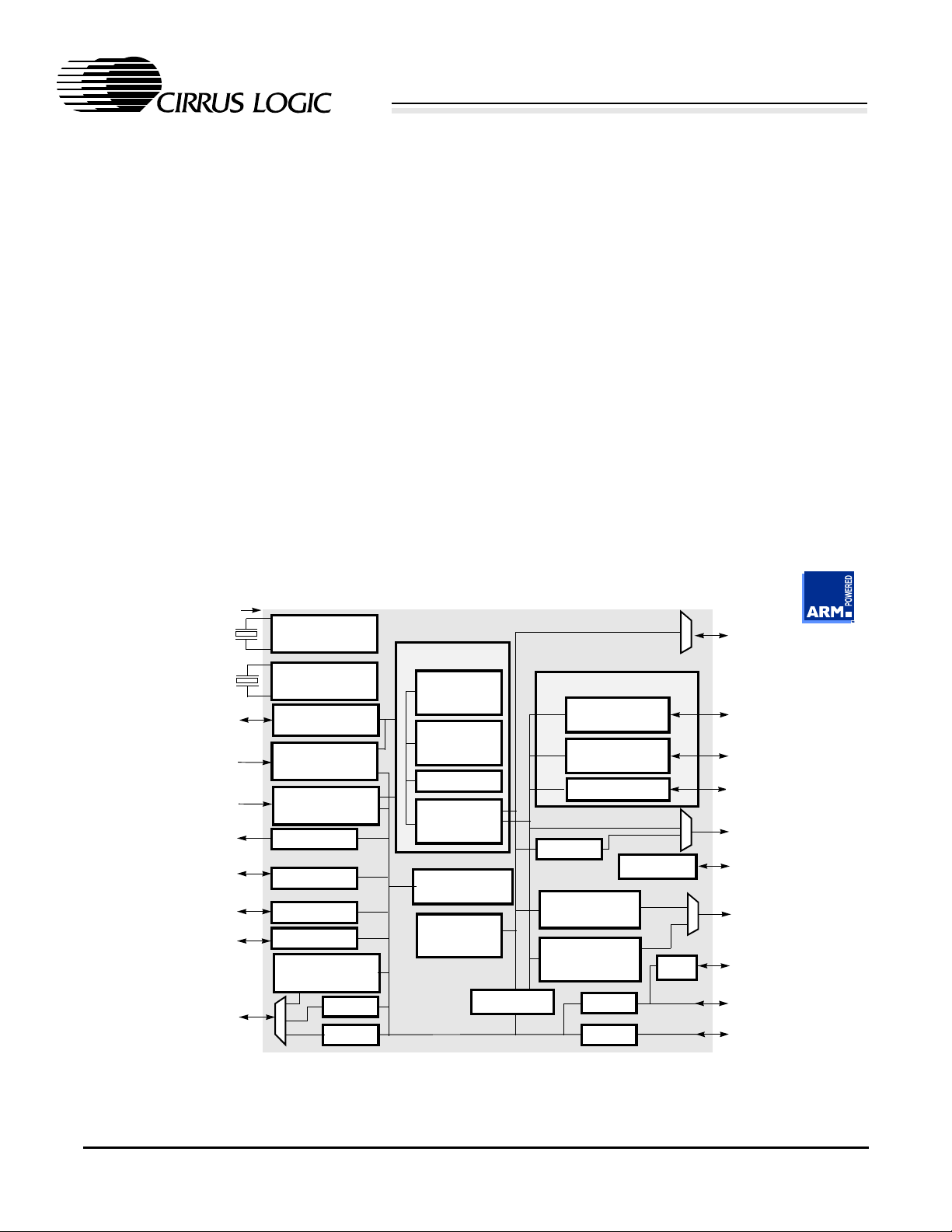
EP7212
• Oscillator and phase-locked loop (PLL) to generate the core clock speeds of 18.432 MHz,
36.864 MHz, 49.152 MHz, and 73.728 MHz
from an external 3.6864 MHz cr ystal, with an
alternative external clock input (used in
13 MHz mode).
• A low power 32.768 kHz oscillator.
The EP7212 design is optimized for low power dissipation and is fabricated on a fully static
0.25 micron CMOS process. It is available in a
256-ball PBGA or a 208-pin LQFP package.
Figure 2 shows a simplified block diagram of the
EP7212. All external memory and peripheral devices are connected to the 32-bit data bus using the
external 28-bit address bus and control signals.
3.1 CPU Core
The ARM720T consists of an ARM7TDMI 32-bit
RISC processor, a unified cache, and a memory
management unit (MMU). The cache is four-way
set associative with 8-kbytes organized as 512 lines
of 4 words. The cache is directly connected to the
ARM7TDMI, and therefore caches the virtual address from the CPU. When the cache misses, the
MMU translates the virtual address into a physical
address. A 64-entry translation lookaside buffer
(TLB) is utilized to speed the address translation
process and reduce bus traffic necessary to read the
page table. The MMU saves power by only translating the cache misses.
See the ARM720T Data sheet for a complete description of the various logic blocks that make up
the processor, as well as all internal registe r information.
13-MHZ INPUT
3.6864 MHZ
32.768 KHZ
NPOR, RUN,
RESET, WAKEUP
BATOK, EXTPWR
PWRFL, BATCHG
EINT[1-3], FIQ,
MEDCHG
FLASHING LED DRIVE
PORTS A, B, D (8-B IT)
PORT E (3-BIT)
KEYBD DRIVERS (0–7)
BUZZER DRIVE
DC-TO-DC
ADCCLK, ADCIN,
ADCOUT, SMPCLK,
ADCCS
SSICLK, SSIT XFR,
SSITXDA, SSIRXDA,
SSIRSFR
PLL
32.768-KHZ
OSCILLATOR
STATE CONTROL
POWER
MANAGEMENT
INTERRUPT
CONTROLLER
RTC
GPIO
PWM
SSI1 (ADC)
DAI
SSI2
CODEC
ARM720T
ARM7TDMI
CPU CORE
8-KBYTE
CACHE
MMU
WRITE
BUFFER
TIMER
COUNTERS (2)
ON-CHIP
BOOT ROM
EPB BRIDGE
EPB BUS
INTERNAL DATA BUS
MEMORY CONTROLLER
CL-PS6700
INTFC.
EXPANSION
CONTROL
DRAM CNTRL
INTERNAL ADDRESS BUS
LCD DMA
ICE-JTAG
LCD
CONTROLLER
ON-CHIP SRAM
38,400 BYTES
UART1
UART2
IrDA
D[0-31]
PB[0:1], NCS[4:5]
EXPCLK, WORD,
NCS[0:3],
EXPRDY, WRITE
MOE, MWE, NRAS[0-1],
NCAS[0-3]
A[0-27],
DRA[0-12]
TEST AND
DEVELOPMENT
LCD DRIVE
LED AND
PHOTODIODE
ASYNC
INTERFACE 1
ASYNC
INTERFACE 2
Figure 2. EP7212 Block Diagram
20 DS474PP1

EP7212
Figure 3. State Diagram
Standby
Operating
Idle
Interrupt or rising wakeup
Write to standby location,
power fail, or user reset
I
n
t
e
r
r
u
p
t
Write to halt location
nPOR, power fail,
or user reset
3.2 State Control
The EP7212 supports the following Power Management States: Operating, Idle, and Standby (see
Figure 3). The normal program execution state is
the Operating State; this is a full performance state
where all of the clocks and peripheral logic are enabled. The Idle State is the same as the Operating
State with the exception of the CPU clock being
halted, and an interrupt or wakeup will return it
back to the Operating State. The Standby State has
the lowest power consumption of the three states.
By selecting this mode the main oscillator shuts
down, leaving only the Real Time Clock and its associated logic powered. It is important when the
EP7212 is in Standby that all power and ground
pins remain connected to power and ground in order to have a proper system wake-up. The only
state that Standby can transition to is the Operating
State.
3.2.1 Standby State
The Standby State equates to the system being
switched "off" (i.e., no display, and the main oscillator is shut down). When the 18.432–73.72 MHz
mode is selected, the PLL will be shut down. In the
13 MHz mode, if the CLKENSL bit is set low, then
the CLKEN signal will be forced low and can, if required, be used to disable an external oscillator.
In the Standby State, all the system memory and
state is maintained and the system time is kept upto-date. The PLL/on-chip oscillator or external oscillator is disabled and the system is static, except
for the low power watch crystal (32 kHz) oscillator
and divider chain to the RTC and LED flasher. The
RUN signal is driven low, therefore this signal can
be used externally in the system to power down
other system modules.
Whenever the EP7212 is in the Standby State, the
external address and data buses are forced low internally by the RUN signal. Thi s i s do ne to preve nt
peripherals that are powered down from draining
current. Also, the internal peripheral’s signals get
set to their Reset State.
In the description below, the RUN/CLKEN pin can
be used either for the RUN functionality, or the
CLKEN functionality to allow an external oscillator to be disabled in the 13 MHz mode. Either RUN
or CLKEN functionality can be selected according
to the state of the CLKENSL bit in the SYSCON2
register. Table 7 on the following page shows peripheral status in various power management
states.
When first powered, or reset by the nPOR (Power
On Reset, active low) signal, the EP7212 is forced
into the Standby State. This is known as a cold reset, and when leaving the Standby State after a cold
reset, external wake up is the only way to wake up
the device. When leaving the Standby State after
non-cold reset conditions (i.e., the software has
forced the device into the Standby State), the transition to the Operating State can be caused by a rising edge on the WAKEUP input signal or by an
enabled interrupt. Normally, when entering the
Standby State from the Operating State, the software will leave some interrupt sources enabled.
NOTE: The CPU cannot be awakened by the TINT,
WEINT, and BLINT interrupts when in the
Standby State.
Typically, software writes to the Standby internal
memory location to cause the transition from the
DS474PP1 21
EP7212
Address (W/B) Operating Idle Standby nPOR
RESET
DRAM Control On On SELFREF Off SELFREF
UARTs On On Off Reset Reset
LCD FIFO On On Reset Reset Reset
LCD On On Off Reset Reset
ADC Interface On On Off Reset Reset
SSI2 Interface On On Off Reset Reset
DAI Interface On On Off Reset Reset
Codec On On Off Reset Reset
Timers On On Off Reset Reset
RTC On On On On On
LED Flasher On On On Reset Reset
DC-to-DC On On Off Reset Reset
CPU On Off Off Reset Reset
Interrupt Control On On On Reset Reset
PLL/CLKEN Signal On On Off Off Off
Table 7. Peripheral Status in Different Power Management States
nURESET
RESET
Operating State to the Standby State. Before entering the Standby State, if external I/O devices (such
as the CL-PS6700s connected to nCS[4] or nCS[5])
are in use, the software must c heck to ensure that
they are idle before issuing the write to the Standby
State location.
Before entering the Standby State, the software
must properly disable the DAI. Failing to do so will
result in higher than expected power consumption
in the Standby State, as well as unpredictable operation of the DAI. The DAI ca n be r e-enabled afte r
transitioning back to the Operating State.
The system can also be forced into the Standby
State by hardware if the nPWRFL or nURESET inputs are forced low. The only exit from the Standby
State is to the Operating State.
The system will only transition to the Operating
State from the Standby State under the following
conditions: when the nPWRFL input pin is high
when the nEXTPWR input pin is low or when the
BATOK input pin is high. This prevents the system
from starting when the power supply is inadequate
(i.e., the main batteries are low), corresponding to
a low level on nPWRFL or BATOK.
From the Standby State, if the WAKEUP signal is
applied with no clock except the 32 kHz clock running, the EP7212 will be initialized into a state
where it is ready to start and is waiting for the CPU
to start receiving its clock. The CPU will still be
held in reset at this point. After the first clock is applied, there will be a delay of about eight clock cycles before the CPU is enabled. This delay is to
allow the clock to the CPU time to settle.
3.2.1.1 UART in Standby State
During the Standby State, the UARTs are disabled
and cannot detect any activity (i.e., start bit) on the
receiver. If this functionality is required then this
can be accomplished in software by the following
method:
1) Permanently connect the RX pin to one of the
active low external interrupt pins.
22 DS474PP1

EP7212
2) Ensure that on entry to the Standby State, the
chosen interrupt source is not masked, and the
UART is enabled.
3) Send a preamble that consists of one start bit,
8 bits of zero, and one stop bit. This will cause
the EP7212 to wake and execute the enabled interrupt vector.
The UART will automatically be re-enabled when
the processor re-enters the Operating State, and the
preamble will be received. Since the UART was
not awake at the start of the pream ble, the timing of
the sample point will be off-center during the preamble byte. However, the next byte transmitted
will be correctly aligned. Thus, the actual first real
byte to be received by the UART will get captured
correctly.
3.2.2 Idle State
If in the Operating State, the I dle State can be en tered by writing to a special internal memory location (HALT) in the EP7212. If an interrupt occurs,
the EP7212 will return immediately back to the Operating State and execute the next instruction. The
WAKEUP signal can not be used to exit the Idle
State. It is only used to exit the Standby State.
In the Idle State, the device functions just like it
does when in the Operating State. However, the
CPU clock is halted while it waits for an event such
as a key press to generate an interrupt. The PLL (in
18.432–73.728 MHz mode) or the external
13 MHz clock source always remains active in the
Idle State.
3.2.3 Keyboard Interrupt
For the case of the keyboard interrupt, the following options are available and are selectable according to bits 1 and 3 of the SYSCON2 register (refer
to the SYSCON2 Register Description for details).
• If the KBWEN bit (SYSCON2 bit 3) is set low,
then a keypress will cause a transition from a
power saving state only if the keyboard interrupt is non-masked (i.e., the interrupt mask register 2 (INTMR2 bit 0) is high).
• When KBWEN is high, a keypress will cause
the device to wake up regardless of the state of
the interrupt mask register. This is called the
“Keyboard Direct Wakeup’ mode. In this
mode, the interrupt request may not get serviced. If the interrupt is masked (i.e., the interrupt mask register 2 (INTMR2 bit 0) is low),
the processor simply starts re-executing code
from where it left off before it entered the power saving state. If the interrupt is non-masked,
then the processor will service the interrupt.
• When the KBD6 bit (SYSCON2 bit 1) is low,
all 8 of Port A inputs are OR’ed together to produce the internal wakeup signal and keyboard
interrupt request. This is the default reset state.
• When the KBD6 bit (SYSCON2 bit 1) is high,
only the lowest 6 bits of Port A are OR’ed together to produce the internal wakeup signal
and keyboard interrupt request. The two most
significant bits of Port A are available as GPIO
when this bit is set high.
In the case where KBWEN is low and the INTMR2
bit 0 is low, it will only be possible to wakeup the
device by using the external WAKEUP pin or another enabled interrupt source. The keyboard interrupt capability allows an OS to use either a polled
or interrupt-driven keyboard routine, or a combination of both.
NOTE: The keyboard interrup t is NOT deglit ch ed.
3.3 Power-Up Sequence
The EP7212 has a power-up sequence that should
be followed for proper start up. If any of the below
recommended timing sequences are violated, then
it is possible that the part may not start-up properly.
This could cause the device to get lost and not recover without a hard reset.
DS474PP1 23

EP7212
1). Upon power, the signal nPOR must be held active (LOW) for a minimum of 100us, after VDD has
become settled.
2). After nPOR goes HIGH, the EP7212 will enter
the Standby State (and only this state). In this state,
the PLL is not enabled, and thus the CPU is not enabled either. The only method that can be used to
allow the EP7212 to exit the Standby State into the
Operating State is by the WAKEUP signal going
active (HIGH).
NOTE: It is not a requirement to use the nURE SET
signal. If not us ed, the nURESET signal
must be HIGH, and it must have gone HIGH
prior to nPOR going HIGH. This is due to the
fact that nURESET is latched into the device
by the rising edge of nPOR. When nURESET is LOW on the rising ed ge of nPOR, it
can force the device into one of its Test
Mode states.
3). After nPOR goes HIGH, the WAKEUP signal
cannot be detected as going HIGH, until after at
least two seconds. After two seconds, the WAKEUP signal can become active, and it must be HIGH
for at least 125us.
4). After the WAKEUP signal is detected internally, it first goes through a deglitching circuit. This is
why is must be active for at least 125us. Then the
PLL gets enabled. WAKEUP is ignored immediately after waking up the system. It also ignores it
while in the Idle or Operating State. It can constantly toggle with no affect on the device. It will only
be read again if nPOR goes low and then high
again, or if software has forced the device back into
the Standby State.
5). A maximum of 250 msec will pass before the
CPU becomes enabled and starts to fetch the first
instruction.
3.4 Resets
There are three asynchronous resets to the EP7212:
nPOR, nPWRFL and nURESET. If any of these are
active, a system reset is generated internally. This
will reset all internal registers in the EP7212 except
the RTC data and match registers. These registers
are only cleared by nPOR allowing the system time
to be preserved through a user reset or power fail
condition.
Any reset will also reset the CPU and cause it to
start execution at the reset vector when the EP7212
returns to the Operating State.
Internal to the EP7212, three different signals are
used to reset storage elements. These are nPOR,
nSYSRES and nSTBY. nPOR is an external signal.
nSTBY is equivalent to the external RUN signal.
nPOR (Power On Reset, active low) is the highest
priority reset signal. When active (low), it will reset
all storage elements in the EP7212. nPOR active
forces nSYSRES and nSTBY active. nPOR will
only be active after the EP7212 is first powered up
and not during any other resets. nPOR active will
clear all flags in the status register except for the
cold reset flag (CLDFLG) bit (SYSFLG, bit 15),
which is set.
nSYSRES (System Reset, active low) is generated
internally to the EP7212 if nPOR, nPWRFL, or
nURESET are active. It is the second highest priority reset signal, used to asynchronously reset most
internal registers in the EP7212. nSYSRES active
forces nSTBY and RUN low. nSYSRES is used to
reset the EP7212 and force it into the Standby State
with no co-operation from software. The CPU is
also reset.
The nSTBY and RUN signals are high when the
EP7212 is in the Operating or Idle States and low
when in the Standby State. The main system clock
is valid when nSTBY is high. The nSTBY signal
will disable any peripheral block that is clocked
from the master clock source (i.e., everything except for the RTC). In general, a system reset will
clear all registers and nSTBY will disable all peripherals that require a main clock. The following
peripherals are always disabled by a low level on
nSTBY: two UARTs and IrDA SIR encoder, timer
counters, telephony codec, and the two SSI inter-
24 DS474PP1

EP7212
faces. In addition, when in the Standby State, the
LCD controller and PWM drive are also disabled.
When operating from an external 13 MHz oscillator which has become disabled in the Standby State
by using the CLKEN (SYSCON, bit 13) signal
(i.e., with CLKENSL = 0), the oscillator must be
stable within 0.125 sec from the rising edge of the
CLKEN signal.
3.5 Clocks
There are two clocking modes for the EP7212. Either an external clock input can be used or the onchip PLL. The clock source is selected by a strapping option on Port E, pin 2 (PE[2]). If PE[2] is
high at the rising edge of nPOR (i.e., upon powerup), the external clock mode is selected. If PE[2] is
low, then the on-chip PLL mode is selected. After
power-up, PE[2] can be used as a GPIO.
The EP7212 device contains several separate sections of logic, each clocked according to its own
clock frequency requirements. When the EP7212 is
in external clock mode, the actual frequencies at
the peripherals will be different than when in PLL
mode. See each peripheral device section for more
details. The section below describes the clocking
for both the ARM720T and address/data bus.
3.5.1 On-Chip PLL
The ARM720T clock can be programmed to
18.432 MHz, 36.864 MHz, 49.152 MHz, or
73.728 MHz with the PLL running at twice the
highest possible CPU clock frequency
(147.456 MHz). The PLL uses an external
3.6864 MHz crystal. By chip default, the on-chip
PLL is used and configured such that the
ARM720T and address/data buses run at
18.432 MHz.
When the clock frequency is selected to be
36 MHz, both the ARM720T and the address/data
buses are clocked at 36 MHz. When the clock frequency is selected higher than 36 MHz, only the
ARM720T gets clocked at this higher speed. The
address/data will be fixed at 36 MHz. The clock
frequency used is selected by programming the
CLKCTL[1:0] bits in the SYSCON3 register. The
clock frequency selection does not effect the EPB
(external peripheral bus). Therefore, all the peripheral clocks are fixed, regardless of the clock speed
selected for the ARM720T.
NOTE: After modifying the CLKCTL[1:0] bits, the
next instruction should always be a ‘NOP’.
3.5.1.1 Characteristics of the PLL Interface
When connecting a crystal to the on-chip PLL interface pins (i.e. MOSCIN and MOSCOUT), the
crystal and circuit should conform to the following
requirements:
• The 3.6864 MHz frequency should be created
by the crystals fundamental tone (i.e., it should
be a fundamental mode crystal).
• A start-up resistor is not necessary, since one is
provided internally.
• Start-up loading capacitors may be placed on
each side of the external crystal and ground.
Their value should be in the range of 10 pF.
However, their values should be selected based
upon the crystal specifications. The total sum of
the capacitance of the traces between the
EP7212’s clock pins, the capacitors, and the
crystal leads should be subtracted from the
crystal’s specifications when determining the
values for the loading capacitors.
• The crystal should have a maximum 100 ppm
frequency drift over the chip’s operating temperature range.
Alternatively, a digital clock source can be used to
drive the MOSCIN pin of the EP7212. With this
approach, the voltage levels of the clock source
should match that of the VDD supply for the
EP7212’s pads (i.e. the supply voltage level used to
drive all of the non-VDD core pins on the EP7212).
DS474PP1 25

EP7212
The output clock pin (i.e., MOSCOUT) should be
left floating.
3.5.2 External Clock Input (13 MHz)
An external 13 MHz crystal oscillator can be used
to drive all of the EP7212. When selected the
ARM720T and the address/data buses both get
clocked at 13 MHz. The fixed clock sources to the
various peripherals will have different frequencies
than in the PLL mode. In this configuration, the
PLL will not be used at all.
NOTE: When operating at 13 MHz, the
CLKCTL[1:0] bits should not be changed
from their default value of ‘00’.
3.5.3 Dynamic Clock Switching When in the PLL Clocking Mode
The clock frequency used for the CPU and the buses is controlled by programming the CLKCTL[1:0]
bits in the SYSCON3 register. When this occurs,
the state controller switches from the current to the
new clock frequency as soon as possible without
causing a glitch on the clock signals. The glitchfree clock switching logic waits until the clock that
is currently in use and the newly programmed clock
source are both low, and then switches from the
previous clock to the new clock without a glitch on
the clocks.
EXPCLK
(internal)
RUN
CLKEN
Interrupt /
WAKEUP
13 MHz
CLKEN
Figure 4. CLKEN Timing Entering the Standby State
Figure 5. CLKEN Timing Entering the Standby State
26 DS474PP1

EP7212
3.6 Interrupt Controller
When unexpected events arise during the execution
of a program (i.e., interrupt or memory fault) an exception is usually generated. When these exceptions occur at the same time, a fixed priority system
determines the order in which they are handled.
Table 8 shows the priority order of all the excep-
tions.
Priority Exception
Highest Reset
. Data Abort
.FIQ
.IRQ
.Prefetch Abort
Lowest Undefined Instruction,
Software Interrupt
Table 8. Exception Priority Handling
The EP7212 interrupt controller has two interrupt
types: interrupt request (IRQ) and fast interrupt request (FIQ). The interrupt controller has the ability
to control interrupts from 22 different FIQ and IRQ
sources. Of these, seventeen are mapped to the IRQ
input and five sources are mapped to the FIQ input.
FIQs have a higher priority than IRQs. If two interrupts are received from within the same group (IRQ
or FIQ), the order in which they are serviced must
be resolved in software. The priorities are listed in
Table 9. All interrupts are level sensitive; that is,
they must conform to the following sequence.
1) The interrupting device (either external or internal) asserts the appropriate interrupt.
2) If the appropriate bit is set in the interrupt mask
register, then either a FIQ or an IRQ will be asserted by the interrupt controller. (A description for each bit in this register can be found in
INTSR1 Interrupt Status Register 1).
3) If interrupts are enabled the processor will
jump to the appropriate address.
4) Interrupt dispatch software reads the interrupt
status register to establish the source(s) of the
interrupt and calls the appropriate interrupt service routine(s).
5) Software in the interrupt service routine will
clear the interrupt source by some action specific to the device requesting the interrupt (i.e.,
reading the UART RX register).
The interrupt service routine may then re-enable interrupts, and any other pending interrupts will be
serviced in a similar way. Alternately, it may re turn
to the interrupt dispatch code, which can check for
any more pending interrupts and dispatch them accordingly. The “End of Interrupt” type interrupts
are latched. All other interrupt sources (i.e., external interrupt source) must be held active until its respective service routine starts executing. See “End
Of Interrupt Locations” on page 83 for more de-
tails.
Table 9, Table 10, and Table 11 show the names
and allocation of interrupts in the EP7212.
3.6.1 Interrupt Latencies in Different
States
3.6.1.1 Operating State
The ARM720T processor checks for a low level on
its FIQ and IRQ inputs at the end of each instruction. The interrupt latency is therefore directly related to the amount of time it takes to complete
execution of the current instruction when the interrupt condition is detected. First, there is a one to
two clock cycle synchronization penalty. For the
case where the EP7212 is operating at 13 MHz
with a 16-bit external memory system, and instruction sequence stored in one wait state FLASH
memory, the worst-case interrupt latency is
251 clock cycles. This includes a dela y for cache
line fills for instruction prefetches, and a data abort
occurring at the end of the LDM instruction, and
the LDM being non-quad word aligned. In addition, the worst-case interrupt latency assumes that
LCD DMA cycles to support a panel size of 320 x
DS474PP1 27
EP7212
Interrupt Bit in INTMR1 and
INTSR1
FIQ 0 EXTFIQ External fast interrupt input (nEXTFIQ pin)
FIQ 1 BLINT Battery low interrupt
FIQ 2 WEINT Tick Watchdog expired interrupt
FIQ 3 MCINT Media changed interrupt
IRQ 4 CSINT Codec sound interrupt
IRQ 5 EINT1 External interrupt input 1 (nEINT[1] pin)
IRQ 6 EINT2 External interrupt input 2 (nEINT[2] pin)
IRQ 7 EINT3 External interrupt input 3 (EINT[3] pin)
IRQ 8 TC1OI TC1 underflow interrupt
IRQ 9 TC2OI TC2 underflow interrupt
IRQ 10 RTCMI RTC compare match interrupt
IRQ 11 TINT 64 Hz tick interrupt
IRQ 12 UTXINT1 Internal UART1 transmit FIFO empty interrupt
IRQ 13 URXINT1 Internal UART1 receive FIFO full interrupt
IRQ 14 UMSINT Internal UART1 modem status changed interrupt
IRQ 15 SSEOTI Synchronous serial interface 1 end of transfer interrupt
Table 9. Interrupt Allocation in the First Interrupt Register
Name Comment
Interrupt Bit in INTMR2 and
INTSR2
IRQ 0 KBDINT Key press interrupt
IRQ 1 SS2RX Master / slave SSI 16 bytes received
IRQ 2 SS2TX Master / slave SSI 16 bytes transmitted
IRQ 12 UTXINT2 UART2 transmit FIFO empty interrupt
IRQ 13 URXINT2 UART2 receive FIFO full interrupt
Table 10. Interrupt Allocation in the Second Interrupt Register
Interrupt Bit in INTMR3 and
INTSR3
FIQ 0 DAIINT DAI interface interrupt
Table 11. Interrupt Allocation in the Third Interrupt Register
Name Comment
Name Comment
28 DS474PP1

EP7212
240 at 4 bits-per-pixel, 60 Hz refresh rate, is in
progress.
This would give a worst-case interrupt latency of
about 19.3 µs for the ARM720T processor operating at 13 MHz in this system. For those interrupt
inputs which have de-glitching, this figure is increased by the maximum time required to pass
through the deglitcher, which is approximately 125
µs (2 cycle of the 16.384 kHz clock derived from
the RTC oscillator). This would create an absolute
worst-case latency of approximately 141 µs. If the
ARM720T is run at 36 MHz or greater and/or
32 bit wide external memory, the 19.3 µs value will
be reduced.
All the serial data transfer peripherals included in
the EP7212 (except for the master-only SSI1) have
local buffering to ensure a reasonable interrupt latency response requirement for the OS of 1 ms or
less. This assumes that the design data rates do not
exceed the data rates described in this specification.
If the OS cannot meet this requirement, there will
be a risk of data over/underflow occurring.
3.6.1.2 Idle State
When leaving the Idle State as a result of an interrupt, the CPU clock is restarted after approximately
two clock cycles. However, there is still potentially
up to 20 µsec latency as desc ribed in the first section above, unless the code is written to include at
least two single cycle instructions immediately after the write to the IDLE register (in which case the
latency drops to a few microseconds). This is important, as the Idle State can only be left because of
a pending interrupt, which has to be synchronized
by the processor before it can be serviced.
3.6.1.3 Standby State
In the Standby State, the latency will depend on
whether the system clock is shut down and if the
FASTWAKE bit in the SYSCON3 register is s et. If
the system is configured to run from the internal
PLL clock, then the PLL will always be shut down
when in the Standby State. In this case, if the
FASTWAKE bit is cleared, then there will be a latency of between 0.125 sec to 0.25 sec. If the
FASTWAKE bit is set, then there will be a latency
of between 250 µsec to 500 µsec. If the system is
running from the external clock (at 13 MHz), with
the CLKENSL bit in SYSCON2 set to 0, then the
latency will also be between 0.125 sec and 0.25 sec
to allow an external oscillator to stabilize. In the
case of a 13 MHz system where the clock is not disabled during the Standby State (CLKENSL = 1),
then the latency will be the same as descri bed in the
Idle State section above.
Whenever the EP7212 is in the Standby State, the
external address and data buses are driven low. The
RUN signal is used internally to force these buses
to be driven low. This is done to prevent peripherals that are power-down from draining current. Also, the internal peripheral’s signals get set to their
Reset State.
Table 12 summarizes the five external interrupt
sources and the effect they have on the processor
interrupts.
3.7 EP7212 Boot ROM
The 128 bytes of on-chip Boot ROM contain an instruction sequence that initializes the device and
then configures UART1 to receive 2048 bytes of
serial data that will then be placed in the on-chip
SRAM. Once the download is complete, execution
jumps to the start of the on-chip SRAM. This
would allow, for example, code to be downloaded
to program system FLASH during a product’s
manufacturing process. See Appendix A: Boot
Code for details of the ROM Boot Code with com-
ments to describe the stages of execution.
Selection of the Boot ROM option is determined by
the state of the nMEDCHG pin during a power on
reset. If nMEDCHG is high while nPOR is active,
then the EP7212 will boot from an external memory device connected to CS[0] (normal boot mode).
DS474PP1 29
EP7212
Interrupt
Pin
nEXTFIQ Not deglitched; must be
nEINT1–2 Not deglitched Worst-case latency
EINT3 Not deglitched Worst-case latency
nMEDCHG Deglitched by 16 kHz
Input State Operating State
Worst-case latency
active for 20 µs to be
detected
clock; must be active
for at least 125 µs to be
detected
of 20 µsec
of 20 µsec
of 20 µsec
Worst-case latency
of 141 µsec
Table 12. External Interrupt Source Latencies
Latency
If nMEDCHG is low, then the boot will be from the
on-chip ROM. Note that in both cases, following
the de-assertion of power on reset, the EP7212 will
be in the Standby State and requires a low-to-high
transition on the external WAKEUP pin in order to
actually start the boot sequence.
The effect of booting from the on-chip Boot ROM
is to reverse the decoding for all chip selects internally. Table 13 shows this decoding. The control
signal for the boot option is latched by nPOR,
which means that the remapping of addresses and
bus widths will continue to apply until nPOR is asserted again. After booting from the Boot ROM,
the contents of the Boot ROM can be read back
from address 0x00000000 onwards, and in normal
state of operation the Boot ROM contents can be
read back from address range 0x70000000.
3.8 Memory and I/O Expansion Interface
Six separate linear memory or expansion segments
are decoded by the EP7212, two of which can be reserved for two PC Card cards, each interfacing to a
separate single CL-PS6700 device. Each segment
is 256 Mbytes in size. Two additional segments
(i.e., in addition to these six) are dedicated to the
on-chip SRAM and the on-chip ROM. The on-chip
ROM space is fully decoded, and the SRAM space
Idle State
Latency
Worst-case
20 µsec: if only
single cycle
instructio ns, less
than 1 µsec
As above As above
As above As above
Worst-case
80 µsec: if only
single cycle
instructions,
125 µsec
0000.0000–0FFF.FFFF CS[7]
1000.0000–1FFF.FFFF CS[6]
2000.0000–2FFF.FFFF nCS[5]
3000.0000–3FFF.FFFF nCS[4]
4000.0000–4FFF.FFFF nCS[3]
5000.0000–5FFF.FFFF nCS[2]
6000.0000–6FFF.FFFF nCS[1]
7000.0000–7FFF.FFFF nCS[0]
Table 13. Chip Select Address Ranges After Boot From
Including PLL / osc. settling time,
approx. 0.25 sec when FASTWAKE = 0,
or approx. 500 µsec when FASTWAKE
= 1, or = Idle State if in 13 MHz mode
with CLKENSL set
As above (note difference if in 13 MHz
mode with CLKENSL set)
Address Range Chip Select
Standby State Latency
(Internal only)
(Internal only)
On-Chip Boot ROM
is fully decoded up to the maximum size of the video frame buffer programmed in the LCDCON register (128 kbytes). Beyond this address range the
SRAM space is not fully decoded (i.e., any accesses beyond 128 kbyte range get wrapped around to
within 128 kbyte range). Any of the six segments
are configured to interface to a conventional
SRAM-like interface, and can be individually programmed to be 8-, 16-, or 32-bits wide, to support
page mode access, and to execute from 1 to 8 wait
states for non-sequential accesses and 0 to 3 for
burst mode accesses. The zero wait state sequential
access feature is designed to support burst mode
30 DS474PP1

EP7212
ROMs. For writable memory devices which use the
nMWE pin, zero wait state sequential accesses are
not permitted and one wait state is the minimum
which should be programmed in the sequential
field of the appropriate MEMCFG register. Bus cycles can also be extended using the EXPRDY input
signal.
Page mode access is accomplished by setting
SQAEN = 1, which enables accesse s of the form
one random address followed by three sequential
addresses, etc., while keeping nCS asserted. These
sequential bursts can be up to four words long before nCS is released to allow DMA and refreshes to
take place. This can significantly improve bus
bandwidth to devices such as ROMs which support
page mode. When SQAEN = 0, all accesses to
memory are by random access without nCS being
de-asserted between accesses. Again nCS is de-asserted after four consecutive accesses to allow
DMAS.
Bits 5 and 6 of the SYSCON2 register independently enable the interfaces to the CL-PS6700 (PC Card
slot drivers). When either of these interfaces are enabled, the corresponding chip select (nCS4 and/or
nCS5) becomes dedicated to that CL-PS6700 interface. The state of SYSCON2 bit 5 determines the
function of chip select nCS4 (i.e., CL-PS6700 interface or standard chip select functionality); bit 6
controls nCS5 in a similar way. There is no i nteraction between these bits.
For applications that require a display buffer smaller than 38,400 bytes, the on-chip SRAM can be
used as the frame buffer.
The width of the boot device can be chosen by selecting values of PE[1] and PE[0] during power on
reset. The inputs in Table 14 are latched by the ris-
ing edge of nPOR to select the boot option.
3.9 DRAM Controller with EDO Support
The DRAM controller in the EP7212 provides all
the connections to directly interface to up to two
PE[1] PE[0] Boot Block
(nCS0)
0 0 32-bit
0 1 8-bit
1 0 16-bit
1 1 Undefined
Table 14. Boot Options
banks of (EDO) DRAM, and the width of the memory interface is programmable to 16-bits or 32-bits.
Both banks have to be of the same width. The
16/32-bit DRAM width selection is made based on
bit 2 of the SYSCON2 register. Each of the two
banks supported can be up to 256 Mbytes in size.
Two RAS lines and four CAS lines are provided,
with one CAS line per byte lane. The DRAM controller does not support device size programmability. Therefore, if two banks are implemented and
DRAM devices are used, a bank smaller than 256
Mbytes would be created leading to a segmented
memory map. Each segmented bank will be separated by 256 Mbytes. Segments that are smaller
than the bank size will repeat within the bank. Ta ble 15. Physical to DRAM Address Mapping
shows the mapping of the physical address to
DRAM row and column addresses. This mapping
has been organized to support any DRAM device
size from 4 Mbits to 1 Gbits with a square row and
column configuration (i.e., the number of column
addresses is equal to the number of row addresses).
If a non-square DRAM is used, further fragmentation of the memory map will occur, however the
smallest contiguous segment will always be 1
Mbyte. With proper mapping of pages/sections by
the MMU, one can create contiguous memory
blocks.
On boot-up, the DRAM controller is configured for
operation with an 18.432 MHz internal bus speed,
and therefore, can support either fast page mode or
EDO DRAM. In this case, the read data from the
DRAM is latched within the EP7212 on the rising
edge of the nCAS output strobes. The DRAM must
DS474PP1 31

EP7212
not have an access time greater than 70 ns in order
to meet the 18 MHz timing requirements. When t he
internal bus is operating at 36.864 MHz (i.e., for
CPU clock frequencies of 36.864, 49.152, or
73.728 MHz), the DRAM controller will only operate with EDO DRAM. When operating at 36
MHz, the EDO DRAM must not have an access
time greater than 50 ns. The DRAM cycle timings
are adjusted to take advantage of the additional performance available from fast EDO DRAM. In EDO
mode, the EP7212 design relies on the DRAM data
being driven to be available on the external data
bus during the entire high phase of the nCAS signal
so that it can be latched towards the end of the cycle. In Fast Page mode, the data should be latched
at the rising edge of nCAS. It is not possible to use
DRAM
Address
Pins
DRAM
Column x16
Mode
DRAM
Column x32
Mode
the EP7212 with fast page mode DRAM at operating frequencies of 36 MHz or higher.
The DRAM controller breaks all sequential access,
so that the minimum page sizes defined can be supported. All of the possible page sizes are multiples
of the minimum page size, so by breaking up accesses on minimum page sizes by default, all accesses crossing larger page boundaries a re broken
up.
Table 16 DRAM Address Mapping f or a 32-Bit
DRAM Memory System shows the address map-
ping for various DRAM’s with square and nonsquare row and address inputs. This assumes two
x16 devices are connected to each RAS line with
32-bit wide DRAM operation selected. This mapping is then repeated every 256 Mbytes for each
DRAM
Row x16
Mode
DRAM
Row x32
Mode
7212 Pin Name
0
1 A2 A3 A10 A11 A[26]/DRA[1]
2 A3 A4 A11 A12 A[25]/DRA[2]
3 A4 A5 A12 A13 A[24]/DRA[3]
4 A5 A6 A13 A14 A[23]/DRA[4]
5 A6 A7 A14 A15 A[22]/DRA[5]
6 A7 A8 A15 A16 A[21]/DRA[6]
7 A8 A9 A16 A17 A[20]/DRA[7]
8 A18 A19 A17 A18 A[19]/DRA[8]
9 A20 A21 A19 A20 A[18]/DRA[9]
10 A22 A23 A21 A22 A[17]/DRA[10]
11 A24 A25 A23 A24 A[16]/DRA[11]
12 A26 A27 A25 A26 A[15]/DRA[12]
1.This bit will be generated by the DRAM controller.
A1
1
Table 15. Physical to DRAM Address Mapping
A2 A9 A10 A[27]/DRA[0]
An example of the DRAM connections for a typical system can be found in Figure 12. A Maximum EP7212
Based System on page 52.
32 DS474PP1

EP7212
DRAM bank. The placeholder ‘n’ below is equal to
0xC + bank number (i.e., 0xC for bank 0, 0xD for
bank 1).
The DRAM controller contains a programmable refresh counter. The refresh rate is controlled using
the DRAM refresh period register (DRFPR).
The 16/32-bit DRAM selection is made based on
bit 2 of the SYSCON2 register. Both banks must
have the same width.
SYSCON2 0x8000 1100
Bit 2 (DRAMSZ) 0 = 32-bit DRAM
1 = 16-bit DRAM
The default is 32-bit width, since the SYSCON2
register is reset to all zeros on power-up.
3.10 CL-PS6700 PC Card Controller Interface
Two of the expansion memory areas are dedicated
to supporting up to two CL-PS6700 PC Card controller devices. These are selected by nCS4 and
nCS5 (must first be enabled by bits 5 and 6 of
SYSCON2). For efficient, low power operation,
both address and data are carried on the lower 16
bits of the EP7212 data bus. Accesses are initiated
by a write or read from the area of memory allocated for nCS4 or nCS5. The memory map within
each of these areas is segmented to allow different
types of PC Card accesses to take place, for attribute, I/O, and common memory space. The CLPS6700 internal registers are memory mapped
within the address space as shown in Table 17.
NOTE: Due to the operating speed of the CL-
PS6700, this interf ace is supported on ly for
processor speeds of 13 and 18 MHz.
EP7212 Size
4 Mbit 9 Row x 9 Column 0.5 Mbyte n000.0000–n007.FFFF 0.5 MByte
16 Mbit 10 Row x 10 Column 2 Mbytes n000.0000–n01F.FFFF 2 Mbytes
16 Mbit 12 Row x 8 Column 2 Mbytes n000.0000–n003.FFFF
64 Mbit 11 Row x 11 Column 8 Mbytes n000.0000–n07F.FFFF 8 Mbytes
64 Mbit 13 Row x 9 Column 8 Mbytes n000.0000–n00F.FFFF
256 Mbit 12 Row x 12 Column 32 Mbytes n000.0000–n1FF.FFFF 32 Mbytes
Address
Configuration
Total Size
of Bank
Address Range of
Segment(s)
n008.0000–n00B.FFFF
n020.0000–n023.FFFF
n028.0000–n02B.FFFF
n080.0000–n083.FFFF
n088.0000–n08B.FFFF
n0A0.0000–n0A3.FFFF
n0A8.0000–n0AB.FFFF
n020.0000–n02F.FFFF
n080.0000–n08F.FFFF
n0A0.0000–n0AF.FFFF
n200.0000–n20F.FFFF
n220.0000–n22F.FFFF
n280.0000–n28F.FFFF
n2A0.0000–n2AF.FFFF
Size of Segment(s)
256 KBytes
256 KBytes
256 KBytes
256 KBytes
256 KBytes
256 KBytes
256 KBytes
256 KBytes
1 MByte
1 MByte
1 MByte
1 MByte
1 MByte
1 MByte
1 MByte
1 MByte
1 Gbit 13 Row x 13 Column 128 Mbytes n000.0000–n7FF.FFFF 128 Mbytes
Table 16. DRAM Address Mapping When Connected to an External 32-Bit DRAM Memory S ystem
DS474PP1 33

EP7212
A complete description of the protocol a nd AC timing characteristics can be found in the CL-PS6700
data sheet. A transaction is initiated by an ac cess to
the nCS4 or nCS5 area. The chip select is asserted,
and on the first clock, the upper 10 bits of the PC
Card address, along with 6 bits of size , space, and
slot information are put out onto the lower 16 bits
of the EP7212’s data bus. Only word (i.e., 4-byte)
and single-byte accesses are supported, and the slot
field is hardcoded to 11, since the slot field is defined as a ‘Reserved field’ by the CL-PS6700. The
chip selects are used to select the device to be accessed. The space field is made directly from the
A26 and A27 CPU address bits, according to the
decode shown in Table 18. T he siz e field is force d
to 11 if a word access is required, or to 00 if a byte
access is required. This avoids the need to configure the interface after a reset. On the second clock
cycle, the remaining 16 bits of the PC Card address
are multiplexed out onto the lower 16 bits of the
data bus. If the transaction selected is a CL-PS6700
register transaction, or a write to the PC Car d (as-
suming there is space available in the CL-PS6700’s
internal write buffer) then the access will continue
on the following two clock cycles. During these
following two clock cycles the upper and lower
halves of the word to be read or written will be put
onto the lower 16 bits of the main data bus.
The ‘ptype’ signal on the CL-PS6700s should be
connected to the EP7212’s WRITE output pin.
During PC Card accesses, the polarity of this pin
changes, and it becomes low to signify a write and
high to signify a read. It is valid with the first half
word of the address. During the second half word
of the address, it is always forced high to indicate
to the CL-PS6700 that the EP7212 has initiated either the write or read.
The PRDY signals from each of the two CLPS6700 devices are connected to Port B bits 0 and
1, respectively. When the PC CARD1 or PC
CARD2 control bits in the SYSCON2 register are
de-asserted, these port bits are available for GPIO.
When asserted, these port bits are used as the
Access Type Addresses for CL-PS6700 Interface 1 Addresses for CL-PS6700 Interface 2
Attribute 0x40000000–0x43FFFFFF 0x50000000– 0x53FFFFFF
I/O 0x44000000–0x47FFFFFF 0x54000000–0x57FFFFFF
Common memory 0x48000000–0x4BFFFFFF 0x58000000–0x5BFFFFFF
CL-PS6700 registers 0x4C000000–0x4FFFFFFF 0x5C000000–0x5FFFFFFF
Table 17. CL-PS6700 Memory Map
Space Field Value PC CARD Memory Space
00 Attribute
01 I/O
10 Common memory
11 CL-PS6700 registers
Table 18. Space Field Decoding
34 DS474PP1

EP7212
PRDY signals. When the PRDY signal is de-asserted (i.e., low), it indicates that the CL-PS6700 is
busy accessing its card. If a PC CARD access is attempted while the device is busy, the PRDY signal
will cause the EP7212’s CPU to be stalled. The
EP7212’s CPU will have to wait for the card to become available. DMA transfers to the LCD can still
continue in the background during this period of
time (as described below). The EP7212 can access
the registers in the CL-PS6700, regardless of the
state of the PRDY signal. If the EP7212 needs to
access the PC CARD via the CL-PS6700, it waits
until the PRDY signal is high before initiating a
transfer request. Once a request is sent, the PRDY
signal indicates if data is available.
In the case of a PC Card write, writes can be posted
to the CL-PS6700 device, with the same timing as
CL-PS6700 internal register writes. Writes will
normally be completed by the CL-PS6700 device
independent of the EP7212 processor activity. If a
posted write times out, or fails to complete for any
other reason, then the CL-PS6700 will issue an interrupt (i.e., a WR_FAIL interrupt). In the case
where the CL-PS6700 write buffer is already full,
the PRDY signal will be de-asserted (i.e., driven
low) and the transaction will be stalled pending an
available slot in the buffer. In this case, the
EP7212’s CPU will be stalled until the write can be
posted successfully. While the PRDY signal is deasserted, the chip select to the CL-PS6700 will be
de-asserted and the main bus will be released so
that DMA transfers to the LCD controller can continue in the background.
In the case of a PC Card read, the PRDY signal
from the CL-PS6700 will be de-asserted until the
read data is ready. At this point, it will be reasserted
and the access will be completed in the same way
as for a register access. In the case of a b yte access,
only one 16-bit data transfer will be required to
complete the access. While the PRDY signal is deasserted, the chip select to the CL-PS6700 will be
de-asserted, and the main bus will be released so
that DMA transfers to the LCD controller can continue in the background.
The EP7212 will re-arbitrate for control of the bus
when the PRDY signal is reasserted to indicate tha t
the read or write transaction can be completed. The
CPU will always be stalled until the PC Card access is completed.
A card read operation may be split into a request
cycle and a data cycle, or it may be combined into
a single request/data transfer cycle. This depends
on whether the data requested from the card is
available in the prefetch buffer (internal to the CLPS6700).
The request portion of the cycle, for a card read, is
similar to the request phase for a card write (described above). If the requested data is available in
the prefetch buffer, the CL-PS6700 asserts the
PRDY signal before the rising edge of the third
clock and the EP7212 continues the cycle to read
the data. Otherwise, the PRDY signal is de-asserted, and the request cycle is stalled. The EP7212
may then allow the DMA address generator to gain
control of the bus, to allow LCD refreshes to continue. When the CL-PS6700 is ready with the data,
it asserts the PRDY signal. The EP7212 then arbitrates for the bus and, once the request is gra nted,
the suspended read cycle is resumed. The EP7212
resumes the cycle by asserting the appropriate chip
select, and data is transferred on the next two
clocks if a word read (one clock if a byte read).
There is no support within the EP7212 for detecting
time-outs. The CL-PS6700 device must be programmed to force the cycle to be completed (with
invalid data for a read) and then generate an interrupt if a read or write access has timed out (i.e.,
RD_FAIL or WR_FAIL interrupt). The system
software can then determine which access was not
successfully completed by reading the status registers within the CL-PS6700.
The CL-PS6700 has support for DMA data transfers. However, DMA is supported only by software
DS474PP1 35

EP7212
emulation because the DMA address generator
built into the EP7212 is dedicated to the LCD controller interface. If DMA is enabled within the CLPS6700, it will assert its PDREQ signal to make a
DMA request. This can be connected to one of the
EP7212’s external interrupts and be used to interrupt the CPU so that the software can service the
DMA request under program control.
Each of the CL-PS6700 devices can generate an interrupt PIRQ. Since the PIRQ signal is an open
drain on the CL-PS6700 devices, two CL-PS6700
devices may be wired OR’ed to the same interrupt.
The circuit can then be connected to one of the
EP7212’s active low external interrupt sources. On
the receipt of an interrupt, the CPU can re ad the interrupt status registers on the CL-PS6700 devices
to determine the cause of the interrupt.
All transactions are synchronized to the EXPCLK
output from the EP7212 in 18.432 MHz mode or
the external 13 MHz clock. The EXPCLK should
be permanently enabled, by setting the EXCKEN
bit in the SYSCON1 register, when the CL-PS6700
is used. The reason for this is that the PC Card interface and CL-PS6700 internal write buffers need
to be clocked after the EP7212 has completed its
bus cycles.
ARM720T control register sets whether the
EP7212 treats words in memory as being stored in
big endian or little endian format. Memory is
viewed as a linear collection of bytes numbered upwards from zero. Bytes 0 to 3 hold the first stored
word, bytes 4 to 7 the second, and so on. In the little
endian scheme, the lowest numbered byte in a word
is considered to be the least significant byte of the
word and the highest numbered byte is the most
significant. Byte 0 of the memory system should be
connected to data lines 7 through 0 (D[7:0]) in this
scheme. In the big endian scheme the most significant byte of a word is stored at the lowest numbered
byte, and the least significant byte is stored at the
highest numbered byte. Therefore, byte 0 of the
memory system should be connected to data lines
31 through 24 (D[31:24]). Load and store are the
only instructions affected by the Endianness.
Tables 19 and 20 demonstrate the behavior of the
EP7212 in big and little endian mode, including the
effect of performing non-aligned word accesses.
The register definition section of this specification
defines the behavior of the internal EP7212 registers in the big endian mode in more detail. For further information, refer to ARM Application Note
61, Big and Little Endian Byte Addressing.
A GPIO signal from the EP7212 can be connected
to the PSLEEP pin of the CL-PS6700 devices to allow them to be put into a power saving state before
the EP7212 enters the Standby State. It is essential
that the software monitor the appropriate status
registers within the CL-PS6700s to ensure that
there are no pending posted bus transactions before
the Standby State is entered. Failure to do this will
result in incomplete PC Card accesses.
3.11 Endianness
The EP7212 uses a little endian configuration for
internal registers. However, it is possible to connect the device to a big endian external memory
system. The big-endian / little-endian bit in the
36 DS474PP1
3.12 Internal UARTs (Two) and SIR Encoder
The EP7212 contains two built-in UARTs that offers similar functionality to National Semiconductor’s 16C550A device. Both UARTs can support
bit rates of up to 115.2 kbits/s and include two 16byte FIFOs: one for receive and one for transmit.
One of the UARTs (UART1) supports the three
modem control input signals CTS, DSR, and DCD.
The additional RI input, and RTS and DTR output
modem control lines are not explicitly supported
but can be implemented using GPIO ports in the
EP7212. UART2 has only the RX and TX pins.

EP7212
Address
(W/B)
Word + 0 (W) 11223344 44 33 22 11 44 33 22 11 11223344 11223344
Word + 1 (W) 11223344 44 33 22 11 44 33 22 11 44112233 44112233
Word + 2 (W) 11223344 44 33 22 11 44 33 22 11 33441122 33441122
Word + 3 (W) 11223344 44 33 22 11 44 33 22 11 22334411 22334411
Word + 0 (H) 11223344 44 33 22 11 44 33 22 11 00001122 00003344
Word + 1 (H) 11223344 44 33 22 11 44 33 22 11 22000011 44000033
Word + 2 (H) 11223344 44 33 22 11 44 33 22 11 00003344 00001122
Word + 3 (H) 11223344 44 33 22 11 44 33 22 11 44000033 22000011
Word + 0 (B) 11223344 dc dc dc 11 44 dc dc dc 00000011 00000044
Word + 1 (B) 11223344 dc dc 22 dc dc 33 dc dc 00000022 00000033
Word + 2 (B) 11223344 dc 33 dc dc dc dc 22 dc 00000033 00000022
Word + 3 (B) 11223344 44 dc dc dc dc dc dc 11 00000044 00000011
NOTE: dc = don’t care
Data in
Memory
(as seen
by the
EP7212)
7:0 15:8 23:16 31:24 7:0 15:8 23: 16 31: 24 Big
Byte Lanes to Memory / Ports / Registers R0 Contents
Big Endian Memory Little Endian Memory
Endian
Table 19. Effect of Endianness on Read Operations
Little
Endian
Address
(W/B)
Word + 0 (W) 11223344 44 33 22 11 44 33 22 11
Word + 1 (W) 11223344 44 33 22 11 44 33 22 11
Word + 2 (W) 11223344 44 33 22 11 44 33 22 11
Word + 3 (W) 11223344 44 33 22 11 44 33 22 11
Word + 0 (H) 11223344 44 33 44 33 44 33 44 33
Word + 1 (H) 11223344 44 33 44 33 44 33 44 33
Word + 2 (H) 11223344 44 33 44 33 44 33 44 33
Word + 3 (H) 11223344 44 33 44 33 44 33 44 33
Word + 0 (B) 11223344 44 44 44 44 44 44 44 44
Word + 1 (B) 11223344 44 44 44 44 44 44 44 44
Word + 2 (B) 11223344 44 44 44 44 44 44 44 44
Word + 3 (B) 11223344 44 44 44 44 44 44 44 44
NOTE: Bold indicates active byte lane.
Register
Contents
Byte Lanes to Memory / Ports / Registers
Big Endian Memory Little Endian Memory
7:0 15:8 23:16 31:24 7:0 15:8 23:16 31:24
Table 20. Effect of Endianness on Write Operations
DS474PP1 37

EP7212
UART operation and line speeds are controlled by
the UBLCR1 (UART bit rate and line control).
Three interrupts can be generated by UART1: RX,
TX, and modem status interrupts. Only two can be
generated by UART2: RX and TX. The RX interrupt is asserted when the RX FIFO becomes half
full or if the FIFO is non-empty for longer than
three character length times with no more characters being received. The TX interrupt is asserted if
the TX FIFO buffer reaches half empty. The modem status interrupt for UART1 is generated if any
of the modem status bits change state. Framing and
parity errors are detected as ea ch byte is received
and pushed onto the RX FIFO. An overrun error
generates an RX interrupt immediately. All error
bits can be read from the 11-bit wide da ta re gister.
The FIFOs can also be programmed to be one byte
depth only (i.e., like a conventional 16450 UART
with double buffering).
The EP7212 also contains an IrDA (Infrared Data
Association) SIR protocol encoder as a post-processing stage on the output of UART1. This encoder can be optionally switched into the TX and RX
signals of UART1, so that these can be used to
drive an infrared interface directly. If the SIR protocol encoder is enabled, the UART TXD1 line is
held in the passive state and transitions of the
RXD1 line will have no effect. The IrDA output pin
is LEDDRV, and the input from the photodiode is
PHDIN. Modem status lines will cause an interrupt
(which can be masked) irrespective of whether the
SIR interface is being used.
Both the UARTs operate in a similar manner to th e
industry standard 16C550A. When CTS is deasserted on the UART, the UART does not stop shifting the data. It relies on software to take
appropriate action in response to the interrupt generated.
Baud rates supported for both the UARTs are dependent on frequency of operation. When operating from the internal PLL, the interface supports
various baud rates from 115.2 kbits/s downwards.
The master clock frequency is chosen so that most
of the required data rates are obtainable exactly.
When operating with a 13.0 MHz external clock
source, the baud rates generated will have a slight
error, which is less than or equal to 0.75%. The
rates (all measured in kbits/s) obtainable from the
13 MHz clock include: 9.6, 19.2, 38, 58, and 115.2.
See UBRLCR1-2 UART1-2 Bit Rate and Line Con-
trol Registers for full details of the available bit
rates in the 13 MHz mode.
3.13 Serial Interfaces
In addition to the two UARTs, the EP7212 offers
the following serial interfaces shown in Table 21.
The inputs / outputs of three of the serial interfaces
(DAI, codec, and SSI2) are multiplexed onto a single set of external interface pins. If the DAISEL bit
of SYSCON3 is low, then either SSI2 or the codec
interface will be selected to connect to the external
pins. When bit 0 of SYSCON2 (SERSEL) is high,
then the codec is connected to the external pins,
when low the master / slave SSI2 is connected to
these pins. When the DAISEL bit is set high, the
DAI interface is connected to the external pins. On
power up, both the DAISEL and SERSEL bits are
reset low, thus the master / slave SSI2 will be connected to these pins (and configured for slave mode
operation to avoid external drive clashes).
Table 22 contains pin definition information for the
three multiplexed interfaces.
The internal names given to each of the t hree inter-
faces are unique to help differentiate them from
each other. The sections below that describe each
of the three interfaces will use their respective
unique internal pin names for clarity.
38 DS474PP1

EP7212
3.13.1 Codec Sound Interface
Transmit and receive modes are enabled by asserting high both the CDENRX and CDENTX codec
The codec interface allows direct connection of a
enable bits in the SYSCON1 register.
telephony type codec to the EP7212. It provides all
the necessary clocks and timing pulses. It also performs a parallel to serial conversion or vice versa
on the data stream to or from the external codec device. The interface is full duplex and contains two
separate data FIFOs (16 deep by 8-bits wide, one
for the receive data, another for the transmit data).
Data is transferred to or from the codec at
64 kbits/s. The data is either written to or read from
the appropriate 16-byte FIFO. If enabled, a codec
interrupt (CSINT) will be generated after every
8 bytes are transferred (FIFO half full/empty). This
means the interrupt rate will be every 1 msec, with
a latency of 1 msec.
NOTE: Both the CDENRX and CDENTX enable bits
should be asserted in tandem for data to be
transmitted or received. The reason for this
is that the interrupt generation will occur
1 msec aft er one of the FIFOs i s enabled.
For example: If the receive FIFO gets
enabled first and the transmit FIFO at a later
time, the interrupt will occur 1 msec after the
receive FIFO is enabled. After the first interrupt occurs, the receive FIFO will be half full.
However, it will not be possible to know how
full the transmit FIF O will be since it was
enabled at a later time. Thus, it is possible to
unintentionally overwrite data already in the
transmit FIFO (See Figure 6).
After the CDENRX and CDENTX enable bits get
asserted, the corresponding FIFOs become enabled. When both FIFOs are disabled, the FIFO sta-
T y pe Comments Referred To As Max. Transfer Speed
SPI / Microwire 1 Master mode only ADC Interface 128 kbits/s
SPI / Microwire 2 Master / slave mode SSI2 Interface 512 kbits/s
DAI Interface CD quality DACs and ADCs DAI Interface 1.536 Mbits/s
Codec Interface Only for use in the PLL clock mode Codec Interface 64 kbits/s
Table 21. Serial Interface Options
Pin
No.
LQFP
63 SSICLK SSICLK = serial bit
65 SSITXFR SSKTXFR = TX
66 SSITXDA SSITXDA = TX
67 SSIRXDA SSIRXDA = RX
68 SSIRXFR SSIRXFR = RX
DS474PP1 39
External
Pin Name
SSI2
Slave Mode
(Internal Name)
clock; Input
frame sync; Input
data; Output
data; Input
frame sync; Input
SSI2
Master Mode
Output PCMCLK =
Output PCMSYNC = Output LRCK = Output 1
Output PCMOUT = Output SDOUT = Output 1
Input PCMIN = Input SDIN = Input
Output p/u
Table 22. Serial-Pin Assignments
Codec
Internal Name
Output
(use a 10k pull-up)
DAI
Internal Name
SCLK =
Output
MCLK 1
Strength
1

EP7212
tus flag CRXFE is set a nd CTXFF is cleared so that
the FIFOs appear empty. Additionally, if the
CDENTX bit is low, the PCMOUT output is disabled. Asserting either of the two enable bits causes
the sync and interrupt generation logic to become
active; otherwise they are disabled to conserve
power.
Data is loaded into the transmit FIFO by writing to
the CODR register. At the beginning of a transmit
cycle, this data is loaded into a shift/load register.
Just prior to the byte being transferred out, PCMSYNC goes high for one PCMCLK cycle. Then the
data is shifted out serially to PCMOUT, MSB first,
(with the MSB valid at the same time PCMSYNC
is asserted). Data is shifted on the rising edge of the
PCMCLK output.
Receiving of data is performed by taking data in serially through PCMIN, again MSB first, shifting it
through the shift/load register and loading the complete byte into the receive FIFO. If there is no data
available in the transmit FIFO, then a zero will be
loaded into the shift/load register. Input data is
sampled on the falling edge of PCMCLK. Data is
read from the CODR register.
3.13.2 Digital Audio Interface
The DAI interface provides a high quality digital
audio connection to DAI compatible audio devices.
The DAI is a subset of I2S audio format that is supported by a number of manufacturers.
The DAI interface produces one 128-bit frame at
the audio sample frequency using a bit clock and
frame sync signal. Digital audio data is transferred,
full duplex, via separate transmit and receive data
lines. The bit clock frequency is either fixed at
9.216 MHz or set via an externally supplied MCLK
signal.
The DAI interface contains separat e transm it and
receive FIFO’s. The transmit FIFO’s are 8 audio
CDENRX
CDENTX
CSINT
1 ms
Interrupt occurs
Figure 6. Codec Interrupt Timing
40 DS474PP1
1 ms
Interrupt occurs
1 ms
Interrupt occurs

EP7212
samples deep and the receive FIFO’s are 12 audio
samples deep.
3.13.2.1 DAI Operation
Following reset, the DAI logic is disabled. To enable the DAI, the applications program should first
clear the emergency underflow and overflow status
bits, which are set following the reset, by writing a
1 to these register bits (in the DAISR register).
Next, the DAI control register should be programmed with the desired mode of operation using
a word write. The transmit FIFOs can either be
“primed” by writing up to eight 16-bit values each,
or can be filled by the normal interrupt service routine which handles the DAI FIFOs. Finally, the
FIFOs for each channel must be enabled via writes
to DAIDR2. At this point, transmission/reception
of data begins on the transmit (SDOUT) and receive (SDIN) pins. This is synchronously controlled by the 9.216 MHz (6.5 MHz in 13 MHz
mode) internal clock or the externally supplied bit
clock (SCLK), and the serial frame clock (LRCK).
3.13.2.2 DAI Frame Format
Each DAI frame is 128 bits long and it comprises
one audio sample. Of this 128-bit frame, only
32 bits are actually used for digital audio data. The
remaining bits are output as zeros. The LRCK signal is used as a frame synchronization signal. Each
transition of LRCK delineates the left and right
halves of an audio sample. When LRCK transitions
from high to low the next 16-bits make up the left
7209
SDIN
SCLK
LRCK
SDOUT
MCLK
DAI ADC
SCLK
LRCK
SDATA
MCLK
DAI DAC
SCLK
LRCK
SDATA
MCLK
CLOCK
GEN
Figure 7. DAI Interface
DS474PP1 41

EP7212
side of an audio sample. When LRCK transitions
from low to high the next 16-bits make up the right
side of an audio sample.
3.13.2.3 DAI Signals
MCLK oversampled clock. Used as an in-
put to the EP7212 for generating the
DAI timing. This signal is also usually used as an input to a DAC/ADC
as an oversampled clock. This signal is fixed at 256 times the audio
sample frequency.
SCLK bit clock. Used as the bit clock input
into the DAC/ADC. This signal is
fixed at 128 times the audio sample
frequency.
LRCK Frame sync. Used as a frame syn-
chronization input to the
DAC/ADC. This signal is fixed at
the audio sample frequency. This
signal is clocked out on the negative
going edge of SCLK.
SDOUT Digital audio data out. Used for
sending playback data to a DAC.
This signal is clocked out on the
negative going edge of the SCLK
output.
SDIN Digital audio input. Used for receiv-
ing record data from an ADC. This
signal is latched by the EP7212 on
the positive going edge of SCLK.
3.13.3 ADC Interface — Master Mode Only SSI1 (Synchronous Serial Interface)
The first synchronous serial interface allows interfacing to the following peripheral devices:
• In the default mode, the device is compatible
with the MAXIM MAX148/9 in external clock
mode. Similar SPI- or Microwire-compatible
devices can be connected directly to the
EP7212.
• In the extended mode and with negative-edge
triggering selected (the ADCCON and ADCCKNSEN bits are set, respectively, in the
SYSCON3 register), this device can be interfaced to Analog Devices’ AD7811/12 chip using nADCCS as a common RFS/TFS line.
• Other features of the devices, including power
management, can be utilized by software and
the use of the GPIO pins.
The clock output frequency is programmable and
only active during data transmissions to save power. There are four output frequencies selectable,
which will be slightly different depending whether
128 SCLKs
LRCK
SCLK
O
SDATA +3 +2 +1+5 +4-1 -2 -3 -4 -5 +3 +2 +1+5 +4-1 -2 -3 -4SDATA +3 +2 +1+5 +4-1 -2 -3 -4 -5 +3 +2 +1+5 +4-1 -2 -3 -4
SDATAI +3 +2 +1+5 +4
42 DS474PP1
MSB
MSB
-1 -2 -3 -4 -5
Figure 8. EP7212 Rev C - Digital Audio Interface Timing – MSB / Left Justified format
Left Channel
LSB
LSB
MSB
MSB
-1 -2 -3 -4
RightChannel
+3 +2 +1+5 +4
LSB
LSB

EP7212
the device is operating in a 13 MHz mode or a
18.432 MHz–73.728 MHz mode (see Table 23).
The required frequency is selected by programming the corresponding bits 16 and 17 in the
SYSCON1 register. The sample clock (SMPCLK)
always runs at twice the frequency of the shift
clock (ADCCLK). The output channel is fed by an
8-bit shift register when the ADCCON bit of
SYSCON3 is clear. When ADCCON is set, up to
16 bits of configuration command can be se nt, as
specified in the SYNCIO register. The input channel is captured by a 16-bit shift register. The clock
and synchronization pulses are activated by a write
to the output shift register. During transfers the
SSIBUSY (synchronous serial interface busy) bit
in the system status flags register is set. When the
transfer is complete and valid data is in the 16-bit
read shift register, the SSEOTI interrupt is assert ed
and the SSIBUSY bit is cleared.
An additional sample clock (SMPCLK) can be enabled independently and is set at twice the transfer
clock frequency.
This interface has no local buffering capability and
is only intended to be used with low bandwidth interfaces, such as for a touch-screen ADC interface.
3.13.4 Master / Slave SSI2 (Synchronous Serial Interface 2)
A second SPI / Microwire interface with full master
/ slave capability is provided by the EP7212. Data
rates in slave mode are theoretically up to
512 kbits/s, full duplex, although continuous operation at this data rate will give an interrupt rate of
2 kHz, which is too fast for many operating systems. This would require a worst-case interrupt response time of less than 0.5 msec and would cause
loss of data through TX underruns and RX overruns.
The interface is fully capable of being clocked at
512 kHz when in slave mode. However, it is anticipated that external hardware will be used to frame
the data into packets. Therefore, although the data
would be transmitted at a rate of 512 kbits/s, the
sustained data rate would in fact only be
85.3 kbits/s (i.e., 1 byte every 750 µsec). At this
data rate, the required interrupt rate will be greater
than 1 msec, which is acceptable.
There are separate half-word-wide RX and TX
FIFOs (16 half-words each) and corresponding interrupts which are generated when the FIFO’s ar e
half-full or half-empty as appropriate. The inter-
SYSCON1
bit 17
00 4.2 4
01 16.9 16
10 67.7 64
1 1 135.4 128
DS474PP1 43
SYSCON1
bit 16
Table 23. ADC Interface Operation Frequencies
13.0 MHz Operation ADCCLK
Frequency (kHz)
18.432–73.728 MHz Operation
ADCCLK Frequency (kHz)

EP7212
rupts are called SS2RX and SS2TX, respectively.
Register SS2DR is used to access the FIFOs.
There are five pins to support this SSI port: SSIRXDA, SSITXFR, SSICLK, SSITXDA, and SSIRX FR. The SSICLK, SSIRXDA, SSIRXFR, and
SSITXFR signals are inputs and the SSITXDA signal is an output in slave mode. In the master mode,
SSICLK, SSITXDA, SSITXFR, and SSIRXFR are
outputs, and SSIRXDA is an input. Master mode is
enabled by writing a one to the SS2MAEN bit
(SYSCON2[9]). When the master / slave SSI is not
required, it can be disabled to save power by writing a zero to the SS2TXEN and the SS2RXEN bits
(SYSCON2[4] [7]). When set, these two bits independently enable the transmit and receive sides of
the interface.
The master / slave SSI is synchronous, full duplex,
and capable of supporting serial data transfers between two nodes. Although the interface is byteoriented, data is loaded in blocks of two bytes at a
time. Each data byte to be transferred is marked by
a frame sync pulse, lasting one clock period, and
located one clock prior to the first bit being transferred. Direction of the SSI2 ports, in slave and
master mode, is shown in Figure 9.
Data on the link is sent MSB first and coincides
with an appropriate frame sync pulse, of one clock
in duration, located one clock prior to the first data
bit sent (i.e., MSB). It is not possible to send data
LSB first.
When operating in master mode, the clock frequency is selected to be the same as the ADC interface’s
(master mode only SSI1) — that is, the frequencies
are selected by the same bits 16 and 17 of the
SYSCON1 register (i.e., the ADCKSEL bits).
Thus, the maximum frequency in master mode is
128 kbits/s. The interface will support continuous
transmission at this rate assuming that the OS can
respond to the interrupts within 1 msec to prevent
over/underruns.
NOTE: To allow synchronization to the incoming
slave clock, the interface enable bits will not
take effect until one SSICLK cycle after they
are written a nd the value read b ack from
SYSCON2. The enable bits reflect the real
status of the enables internally. Hence, there
will be a delay before the new value programmed to the enable bits can be read
back.
The timing diagram for this interface can be found
in the AC Characteristics section of this document.
3.13.4.1 Read Back of Residual Data
All writes to the transmit FIFO must be in halfwords (i.e., in units of two bytes at a time). On the
receive side, it is possible that an odd number of
bytes will be received. Bytes are always loaded into
the receive FIFO in pairs. Consequently, in the case
of a single residual byte remaining at the end of a
transmission, it will be necessary for the software
Slave 7212
SSIRXFR
SSITXFR
SSICLK
SSIRXDA
SSITXDA
Figure 9. SSI2 Port Directions in Slave and Master Mode
44 DS474PP1
Master 7212
SSIRXFR
SSITXFR
SSICLK
SSITXDA
SSIRXDA

EP7212
to read the byte separately. This is done by reading
the status of two bits in the SYSFLG2 register to
determine the validity of the residual data. These
two bits (RESVAL, RESFRM) are both set high
when a residual is valid. RESVAL is cleared on either a new transmission or on reading of the r esidual bit by software. RESFRM is cleared only on a
new transmission. By popping the residual byte
into the RX FIFO and then reading the status of
these bits it is possible to determine if a residual bit
has been correctly read.
Figure 10 illustrates this procedure. The sequence
is as follows: read the RESVAL bit, if this is a 0, no
action needs to be taken. If this is a 1, then pop the
residual byte into the FIFO by writing to the
SS2POP location. Then read back the two status
bits RESVAL and RESFRM. If these bits read back
01, then the residual byte popped into the FIFO is
valid and can be read back from the SS2DR register. If the bits are not 01, then there has been another transmission received since the residual read
procedure has been started. The data item that has
been popped to the top of the FIFO will be invalid
and should be ignored. In this case, the correct byte
will have been stored in the most significant byte of
the next half-word to be clocked into the FIFO.
NOTE: All the writes / reads to the FIFO are done
word at a time (data on the lower 16 bits is
valid and upper 16 bits are ignored).
Software manually pops the residual byte into the
RX FIFO by writing to the SS2POP location (the
value written is ignored). This write will strobe the
RX FIFO write signal, causing the residual byte to
be written into the FIFO.
Figure 10. Residual Byte Reading
3.13.4.2 Support for Asymmetric Traffic
The interface supports asymmetric traffic (i.e., unbalanced data flow). This is accomplished through
separate transmit and receive frame sync control
lines. In operation, the receiving node receives a
byte of data on the eight clocks following the asser-
Residual bit valid
00
New RX byte
received
New RX byte received
01
11
Pop FIFO
tion of the receive frame sync c ontrol line. In a similar fashion, the sending node can transmit a byte of
data on the eight clocks following the assertion of
the transmit frame sync pulse. There is no correlation in the frequency of assertions of the RX and
TX frame sync control lines (SSITXFR and
SSIRXFR). Hence, the RX path may bear a greater
data throughput than the TX path, or vice versa.
Both directions, however, have an absolute maximum data throughput rate determined by the maximum possible clock frequency, assuming that the
interrupt response of the target OS is sufficiently
quick.
3.13.4.3 Continuous Data Transfer
Data bytes may be sent / received in a contiguous
manner without interleaving clocks between bytes.
The frame sync control line(s) are eight clocks
apart and aligned with the clock representing bit D0
of the preceding byte (i.e., one bit in advance of the
MSB).
3.13.4.4 Discontinuous Clock
In order to save power during the idle times, the
clock line is put into a static low state. The master
is responsible for putting the link into the Idle State.
The Idle State will begin one clock, or more, after
the last byte transferred and will resume at least one
clock prior to the first frame sync assertion. To disable the clock, the TX section is turned off.
In Master mode, the EP7212 does not support the
discontinuous clock.
DS474PP1 45

EP7212
3.13.4.5 Error Conditions
RX FIFO overflows are detected and conveyed via
a status bit in the SYSFLG2 register. This register
should be accessed at periodic intervals by the application software. The status register should be
read each time the RX FIFO interrupts are generated. At this time the error condition (i.e., overrun
flag) will indicate that an error has occurred but
cannot convey which byte contains the error. Writing to the SRXEOF register location clears the
overrun flag. TX FIFO underflow condition is detected and conveyed via a bit in the SYSFLG2 register, which is accessed by the application software.
A TX underflow error is cleared by writing data to
be transmitted to the TX FIFO.
3.13.4.6 Clock Polarity
Clock polarity is fixed. TX data is presented on the
bus on the rising edge of the clock. Data is latched
into the receiving device on the falling edge of the
clock. The TX pin is held in a tristate condition
when not transmitting.
3.14 LCD Controller with Support for OnChip Frame Buffer
The LCD controller provides all the necessary control signals to interface directly to a single panel
multiplexed LCD. The panel size is programmable
and can be any width (line length) from 32 to
1024 pixels in 16-pixel increments. The total video
frame buffer size is programmable up to 128
kbytes. This equates to a theoretical maximum panel size of 1024 x 256 pixels in 4 bits-per-pixel
mode. The video frame buffer can be located in any
portion of memory controlled by the chip selects.
Its start address will be fixed at address 0x0000000
within each chip select. The start address of the
LCD video frame buffer is defined in the FBADDR[3:0] register. These bits become the most significant nibble of the external address bus. The
default start address is 0xC000 0000 (FBADDR =
0xC). A system built using the on-chip SRAM
(OCSR), will then serve as the LCD video frame
buffer and miscellaneous data store. The LCD video frame buffer start address should be set to 0x6 in
this option. Programming of the register FBADDR
is only permitted when the LCD is disabled (this is
to avoid possible cycle corruption when changing
the register cont en t s while a LCD DMA cycle is in
progress). There is no hardware protection to prevent this. It is necessary for the software to disable
the LCD controller before reprogramming the
FBADDR register. Full address decoding is provided for the OCSR, up to the maximum video
frame buffer size programmable into the LCDCON
register. Beyond this, the address is wrapped
around. The frame buffer start address must not be
programmed to 0x4 or 0x5 if either CL-PS6700 interface is in use (PCMEN1 or PCMEN2 bits in the
SYSCON2 register are enabled). FBADDR should
never be programmed to 0x7 or 0x8, as these are
the locations for the on-chip Boot ROM and internal registers.
The screen is mapped to the video frame buffer as
one contiguous block where each horizontal line of
pixels is mapped to a set of consecutive bytes or
words in the video RAM. The video frame buffer
can be accessed word wide as pixel 0 is mapped to
the LSB in th e buffer such that the pixels are arranged in a little endian manner.
The pixel bit rate, and hence the LCD refresh rate,
can be programmed from 18.432 MHz to 576 kHz
when operating in 18.432–73.728 MHz mode, or
13 MHz to 203 kHz when operating from a
13 MHz clock. The LCD controller is programmed
by writing to the LCD control register (LCDCON).
The LCDCON register should not be reprogrammed while the LCD controller is enabled.
The LCD controller also contains two 32-bit palette
registers, which allow any 4-, 2-, or 1-bit pixel value to be mapped to any of the 15 grayscale values
available. The required DMA bandwidth to support
a ½ VGA panel displaying 4 bits-per-pixel da ta at
46 DS474PP1

EP7212
an 80 Hz refresh rate is approximately
6.2 Mbytes/sec. Assuming the frame buffer is
stored in a 32-bit wide the maximum theoretical
bandwidth available is 86 Mbytes/sec at
36.864 MHz, or 29.7 Mbytes/sec at 13 MHz.
The LCD controller uses a nine stage 32-bit wide
FIFO to buffer display data. The LCD controller requests new data when there are five words remaining in the FIFO. This means that for a ½ VGA
display at 4 bits-per-pixel and 80 Hz refresh rate,
the maximum allowable DMA latency is approximately 3.25 µsec ((5 words
240 x 4bpp x 80 Hz)) = 3.25 µsec). The worst-case
latency is the total nu mber of cycl es from when the
DMA request appears to when the first DMA data
word actually becomes available at the FIFO.
DMA has the highest priority, so it will always happen next in the system. The maximum number of
cycles required is 36 from the point at which the
DMA request occurs to the point at which the STM
is complete, then another 6 cycles before the data
actually arrives at the FIFO from the first DMA
read. This creates a total of 42 cycles. Assuming
the frame buffer is located in 32-bit wide, the
worst-case latency is almost exactly 3.2 µs, with
13 MHz page mode cyc les. With each cycle consuming ~77 ns (i.e., 1/1 MHz), the value of 3.2 µs
comes from 42 cycles x 77 ns/cycle = ~3.23 µsec.
If 16-bit wide, then the worst-case latency will double. In this case, the maximum permissible display
size will be halved, to approximately 320 x 240 pixels, assuming the same pixel depth and refresh rate
has to be maintained. If the frame buffer is to be
stored in static memory, then further calculations
must be performed. If 18 MHz mode is selected,
and 32-bit wide, then the worst-case latency will be
2.26 µsec (i.e., 42 cycles x 54 nsec/cycle). If
36 MHz mode is selected, and 32-bit wide, then the
worst-case latency drops down to 1.49 µs. This calculation is a little more comple x for 36 MHz mode
of operation. The total number of cycles = (12 x 4)
+ 7 = 55. Thus, 55 x 27 ns = ~1.49 µsec.
x 8 bits/byte) / (640 x
Figure 11 shows the organization of the video map
for all combinations of bits-per-pixel.
The refresh rate is not affected by the number of
bits-per-pixel; however the LCD controller fetches
twice the data per refresh for 4 bit s-per- pixe l compared to 2 bits-per-pixel. The main reason for reducing the number of bits-per-pixel is to reduce the
power consumption of the memory where the video
frame buffer is mapped.
3.15 Timer Counters
Two identical timer counters are integrated into the
EP7212. These are referred to as TC1 and TC2.
Each timer counter has an associated 16-bit read /
write data register and some control bi ts in the system control register. Each counter is loaded with
the value written to the data register immediately.
This value will then be decremented on the second
active clock edge to arrive after the write (i.e., after
the first complete period of the clock). When the
timer counter under flows (i.e., reaches 0), it w ill
assert its appropriate interrupt. The timer counters
can be read at any time. The clock source and mode
are selectable by writing to various bits in the system control register. When run from the internal
PLL, 512 kHz and 2 kHz rates are provided. When
using the 13 MHz external source, the default frequencies will be 541 kHz and 2.115 kHz, respectively. However, only in non-PLL mode, an
optional divide by 26 frequency can be generated
(thus generating a 500 kHz frequency when using
the 13 MHz source). This divider is enabled by setting the OSTB (Operating System Timing Bit) in
the SYSCON2 register (bit 12). When this bit is set
high to select the 500 kHz mode, the 500 kHz frequency is routed to the timers instead of the
541 kHz clock. This does not affect the frequencies
derived for any of the other internal peripherals.
The timer counters can operate in two modes: fre e
running or pre-scale.
DS474PP1 47

EP7212
3.15.1 Free Running Mode
In the free running mode, the counter will wrap
around to 0xFFFF when it under flows and it will
continue to count down. Any value written to TC1
or TC2 will be decremented on the second edge of
the selected clock.
Pixel 1 Pixel 2 Pixel 3 Pixel 4
Gray scale
Bit 0 Bit 1 Bit 2 Bit 3 Bit 4 Bit 5 Bit 6 Bit 7
4 Bits per pixel
3.15.2 Prescale Mode
In the prescale mode, the value written to TC1 or
TC2 is automatically re-loaded when the counter
under flows. Any value written to TC1 or TC2 will
be decremented on the second edge of the selected
clock. This mode can be used to produce a programmable frequency to drive the buzzer (i.e., with
TC1) or generate a periodic interrupt. The formula
is F=(500 kHz) / (n+1).
Gray scale
Pixel 1 Pixel 2 Pixel 3 Pixel 4
Gray scale Gray scale
Bit 0 Bit 1 Bit 2 Bit 3 Bit 4 Bit 5 Bit 6 Bit 7
Gray scale Gray scale
2 Bits per pixel
Pixel 1 Pixel 2 Pixel 3 Pixel 4
Gray scale Gray scale
Bit 0 Bit 1 Bit 2 Bit 3 Bit 4 Bit 5 Bit 6 Bit 7
Gray scale Gray scale
1 Bit per pixel
Figure 11. Video Buffer Mapping
48 DS474PP1

EP7212
3.16 Real Time Clock
The EP7212 contains a 32-bit Real Time Clock
(RTC). This can be written to and read from in the
same way as the timer counters, but it is 32 bits
wide. The RTC is always clocked at 1 Hz, generated from the 32.768 kHz oscillator. It also contains
a 32-bit output match register, this can be programmed to generate an interrupt when the time in
the RTC matches a specific time written t o this register. The RTC can only be reset by an nPOR cold
reset. Because the RTC data register is updated
from the 1 Hz clock derived from the 32 kHz
source, which is asynchronous to the main memory
system clock, the data register should always be
read twice to ensure a valid and stable reading. This
also applies when reading back the RTCDI V field
of the SYSCON1 register, which reflects the status
of the six LSBs of the RTC counter.
3.16.1 Characteristics of the Real Time Clock Interface
When connecting a crystal to the RTC interface
pins (i.e., RTCIN and RTCOUT), the crystal and
circuit should conform to the following requirements:
• The 32.768 kHz frequency should be created
by the crystals fundamental tone (i.e., it should
be a fundamental mode crystal)
• A start-up resistor is not necessary, since one is
provided internally.
• Start-up loading capacitors may be placed on
each side of the external crystal and ground.
Their value should be in the range of 10 pF.
However, their values should be selected based
upon the crystal specifications. The total sum of
the capacitance of the traces between the
EP7212’s clock pins, the capacitors, and the
crystal leads should be subtracted from the
crystal’s specifications when determining the
values for the loading capacitors.
• The crystal should have a maximum 5 ppm frequency drift over the chip’s operating temperature range.
• The voltage for the crystal must be 2.5 V + 0.2 V.
Alternatively, a digital clock source can be used to
drive the RTCIN pin of the EP7212. With this approach, the voltage levels of the clock source
should match that of the VDD supply for the
EP7212’s pads (i.e., the supply voltage level used
to drive all of the non-VDD core pins on the
EP7212) (i.e., RTCOUT). The output clock pin
should be left floating.
3.17 Dedicated LED Flasher
The LED flasher feature enables an external pin
(PD[0] / LEDFLSH) to be toggled at a programmable rate and duty ratio, with the intention that the
external pin is connected to an LED. This module
is driven from the RTCs 32.768 kHz oscillator and
works in all running modes because no CPU intervention is needed once its rate and duty ratio have
been configured (via the LEDFLSH register). The
LED flash rate period can be programmed for 1, 2,
3, or 4 seconds. The duty ratio can be programmed
such that the mark portion can be 1/16, 2/16…
16/16 of the full cycle. The external pin can provide
up to 4 mA of drive current.
3.18 Two PWM Interfaces
Two Pulse Width Modulator (PWM) duty ratio
clock outputs are provided by the EP7212. When
the device is operating from the internal PLL, the
PWM will run at a frequency of 96 kHz. These signals are intended for use as drives for external DCto-DC converters in the Power Supply Unit (PSU)
subsystem. External input pins that would normally
be connected to the output from comparators monitoring the external DC-to-DC converter output are
also used to enable these clocks. These are the
FB[0:1] pins. The duty ratio (and hence PWMs on
time) can be programmed from 1 in 16 to 15 in 16.
The sense of the PWM drive signal (active high or
DS474PP1 49

EP7212
low) is determined by latching the state of this
drive signal during power on reset (i.e., a pull-up on
the drive signal will result in a active low drive output, and visa versa). This allows either positive or
negative voltages to be generated by the external
DC-to-DC converter. PWMs are disabled by writing zeros into the drive ratio fields in the PMPCON
Pump Control register.
NOTE: To maximiz e power savings, the d rive ratio
fields should be used to disable the PWMs,
instead of the FB pins. The clocks that
source the PWMs are disabled when the
drive ratio fields are zeroed.
3.19 Boundary Scan
IEEE 1149.1 compliant JTAG is provided with the
EP7212. Table 24 shows what instructions are supported in the EP7212.
Instruction Code Description
EXTEST
SCAN_N
SAMPLE / PRELOAD
IDCODE
BYPASS
Table 24. Instructions Supported in JTAG Mode
The INTEST function will not be supported for the
EP7212.
Additional user-defined instructions exist, but
these are not relevant to board-level testing. For
0000
0010
0011
1110
1111
Places the selected
scan chain in test
mode.
Connects the Scan
Path Register between
TDI and TDO
NOTE: This instruction is included for
product testing only
and should never be
used.
Connects the ID register between TDI and
TDO
Connects a 1-bit shift
register bit TDI and
TDO
further information please refer to the ARM DDI
0087E ARM720T Data Sheet.
As there are additional scan-chains within the
ARM720T processor, it is necessary to include a
scan-chain select function — shown as SCAN_N
in Table 24. To select a pa rticular scan chain, this
function must be input to the TAP controller, followed by the 4-bit scan chain identification code.
The identification code for the boundary scan chain
is 0011.
Note that it is only necessary to issue the SCAN_N
instruction if the device is already in the JTAG
mode. The boundary scan chain is selected as the
default on test-logic reset and any of the system resets.
The contents of the device ID-register for the
EP7212 are shown in Table 25. This is equivalent
to 0x0F0F0F0F. Note this is the ID-code for the
ARM720T processor.
3.20 In-Circuit Emulation
3.20.1 Introduction
EmbeddedICE™ is an extension to the architecture
of the ARM family of processors, and provides the
ability to debug cores that are deeply embedded
into systems. It consists of three parts:
1) A set of extensions to the ARM core
2) The EmbeddedICE macrocell, which provides
external access to the extensions
3) The EmbeddedICE interface, which provides
communication between the host computer and
the EmbeddedICE macrocell
The EmbeddedICE macrocell is programmed, in a
serial fashion, through the TAP controller on the
ARM via the JTAG interface. The EmbeddedICE
macrocell is by default disable d to minimiz e power
usage, and must be enabled at boot-up to support
this functionality.
50 DS474PP1

EP7212
3.20.2 Functionality
The ICEBreaker module consists of two real-time
watchpoint units together with a control and status
register. One or both of the units can be programmed to halt the execution of the instructions
by the ARM processor. Execution is halted when
either a match occurs between the values programmed into the ICEBreaker and the values currently appearing on the address bus, data bus, and
the various control signals. Any bit can be masked
to remove it from the comparison. Either unit can
be programmed as a watchpoint (monitoring data
accesses) or a breakpoint (monitoring instruction
fetches).
Using one of these watchpoint units, an unlimited
number of software breakpoints (in RAM) can be
supported by substitution of the actual code.
NOTE: The EXTERN[1:0] signals from the ICE-
Breaker module are not wired out in this
device. This mechanism is used to allow
watchpoints to be dependent on an exter nal
event. This behavior can be emulated in
software via the ICEBreaker c ontrol registers.
A more detailed description is available in the
ARM Software Development Toolkit User Guide
and Reference Manual. The ICEBreaker module
and its registers are fully described in the
ARM7TDMI Data Sheet.
3.21 Maximum EP7212-Based System
A maximum configured system using the EP7212
is shown in Figure 12. This system assumes all of
the DRAMs and ROMs are 16-bit wide devices.
The keyboard may be connected to more GPIO bits
than shown to allow greater than 64 keys, however
these extra pins will not be wired into the WAKEUP pin functionality.
Version Part number Manufacturer ID
00001111000011110000111100001111
Table 25. Device ID Register
DS474PP1 51

EP7212
CRYSTAL
CRYSTAL
PC CARD
SOCKET
EXTERNAL MEMORY-
MAPPED EXPANSION
ADDITIONAL I/O
CL-PS6700
CONTROLLER
×16
DRAM
×16
DRAM
×16
FLASH
×16
FLASH
PC CARD
×16
DRAM
×16
DRAM
×16
FLASH
×16
FLASH
BUFFERS
BUFFERS
AND
LATCHES
MOSCIN
RTCIN
nCS[4]
PB0
EXPCLK
D[31:0]
A[27:0]
nMOE
WRITE
nRAS[1]
nRAS[0]
nCAS[0]
nCAS[1]
nCAS[2]
nCAS[3]
nCS[0]
nCS[1]
CS[n]
WORD
NCS[2]
NCS[3]
LEDFLSH
nEXTPWR
EP7212
nBATCHG
DRIVE[1:0]
DD[3:0]
CL1
CL2
FM
COL[7:0]
PA[7:0]
PB[7:0]
PD[7:0]
PE[2:0]
nPOR
nPWRFL
BATOK
RUN
WAKEUP
FB[1:0]
DAISSI-
CLK
SSITXFR
SSITXDA
SSIRXDA
LEDDRV
PHDIN
RXD1/2
TXD1/2
DSR
CTS
DCD
ADCCLK
nADCCS
ADCOUT
ADCIN
SMPCLK
LCD
M
KEYBOARD
POWER
SUPPLY UNIT
DC
INPUT
AND
COMPARATORS
BATTERY
DC-TO-DC
CONVERTERS
CODEC/SSI2/
DAI
IR LED AND
PHOTODIODE
2× RS-232
TRANSCEIVERS
ADC
DIGITIZER
NOTE: A system can only use one of the following
peripheral interfa ces at any given time:
SSI2, codec, or
DAI.
Figure 12. A Maximum EP7212 Based System
52 DS474PP1

EP7212
4. MEMORY MAP
The lower 2 GByte of the address space is allocated
to memory. The 0.5 GByte of address space from
0xC0000000 to 0xDFFFFFFF is allocated to
DRAM. The 1.5 GByte, less 8 kbytes for internal
registers, is not accessible in the EP7212. The
MMU in the EP7212 should be programmed to
generate an abort exception for access to this area.
Internal peripherals are addressed through a set of
internal memory locations from hex address
0x8000.0000 to 0x8000.3FFF. These are known as
the internal registers in the EP7212. In Table 26,
the memory map from 0x8000.000 to
0x8000.1FFF contains registers that are compatible
with the CL-PS7111 (see Table 26). These were in-
Address Contents Size
0xF000.0000 Reserved 256 Mbytes
0xE000.0000 Reserved 256 Mbytes
0xD000.0000 DRAM Bank 1 256 Mbytes
0xC000.0000 DRAM Bank 0 256 Mbytes
0x8000.4000 Unused ~1 Gbyte
0x8000.2000
Internal registers (new)
cluded for backward compatibility and are refe rred
to as old internal registers.
Table 26 shows how the 4-G byte address range of
the ARM720T processor (as configured within this
chip) is mapped in the EP7212. The memory map
shown assumes that two CL-PS6700 PC Card controllers are connected. If this func tionality is not required, then the nCS[4] and nCS[5] memory is
available. The external boot ROM is not fully decoded (i.e., the boot code will repeat within the
256-Mbyte space from 0x70000000 to
0x80000000). See Table 13 on page 30 for the
memory map when booted from on chip boot
ROM. The SRAM is fully decoded up to a maximum size of 128 kbytes. Access to any location
above this range will be wrapped to within the
range.
8 kbytes
0x8000.0000
0x7000.0000 Boot ROM (nCS[7]) 128 bytes
0x6000.0000 SRAM (nCS[6]) 38,400 bytes
0x5000.0000 PCMCIA-1 (nCS[5]) 4 x 64 Mbytes
0x4000.0000 PCMCIA-0 (nCS[4]) 4 x 64 Mbytes
0x3000.0000 Expansion (nCS[3]) 256 Mbytes
0x2000.0000 Expansion (nCS[2]) 256 Mbytes
0x1000.0000 ROM Bank 1 (nCS[1]) 256 Mbytes
0x0000.0000 ROM Bank 0 (nCS[0]) 256 Mbytes
Table 26. EP7212 Memory Map in External Boot Mode
DS474PP1 53
Internal registers (old)
(from 7111)
8 kbytes

EP7212
5. REGISTER DESCRIPTIONS
5.1 Internal Registers
Table 27 shows the Internal Registers of the
EP7212 that are compatible with the CL-PS7111
when the CPU is configured to a little endian m emory system. Table 28 shows the differences that occur when the CPU is configured to a big endian
memory system for byte-wide access to Ports A, B,
and D. All the internal registers a re inhere ntly little
endian (i.e., the least significant byte is attached to
bits 7 to 0 of the data bus). Hence, the system Endianness affects the addresses required for byte accesses to the internal registers, resulting in a
reversal of the byte address required to read / write
a particular byte within a register. Note that the internal registers have been split into two groups –
the “old” and the “new”. The old ones are the same
as that used in CL-PS7111 and are there for c ompatibility. The new registers are for accessing the
additional functionality of the DAI interface and
the LED flasher.
There is no effect on the register addresses for word
accesses. Bits A[0:1] of the internal address bus are
only decoded for Ports A, B, and D (to allow read /
write to individual ports). For all other registers,
bits A[0:1] are not decoded, so that byte reads will
return the whole register contents onto the
EP7212’s internal bus, from where the appropriate
byte (according to the endianness) will be read by
the CPU. To avoid the additional complexity, it is
preferable to perform al l internal register a ccesses
as word operations, except for ports A to D which
are explicitly designed to operate with byte ac cesses, as well as with word accesses.
An 8 k segment of memory in the range
0x8000.0000 to 0x8000.3FFF is reserved for internal use in the EP7212. Accesses in this range will
not cause any external bus activity unless debug
mode is enabled. Writes to bits that are not explic-
itly defined in the internal area are legal and will
have no effect. Reads from bits not explicitly defined in the internal area are legal but will read undefined values. All the internal addresses should
only be accessed as 32-bit words and are always on
a word boundary, except for the PIO port registers,
which can be accessed as bytes. Address bits in the
range A[0:5] are not decoded (except for Ports
A–D), this means each internal register is valid for
64 bytes (i.e., the SYSFLG1 register appears at locations 0x8000.0140 to 0x8000.017C). There are
some gaps in the register map for backward compatibility reasons, but registers located next to a
gap are still only decoded for 64 bytes.
The GPIO port registers are byte-wide and can be
accessed as a word but not as a half-word. These
registers additionally decode A[0:1]. All addresses
are in hexadecimal notation.
NOTE: All byte-wide regis ters should be accessed
as words (except Port A to Port D registers,
which are designed to work in both word and
byte modes).
All registers bit alignment starts from the
LSB of the register (i.e., they are all right shift
justified).
The registers whic h i nte ra ct with the 32 kHz
clock or which could change during readback (i.e., RTC data registers, SYSFLG1
register (lower 6-bits only), the TC1D and
TC2D data registers, port registers, and
interrupt status registers), should be read
twice and compared to ens ure that a stable
value has been read back.
All internal registers in the EP7212 are reset
(cleared to zero) by a system reset (i.e., nPOR,
nRESET, or nPWRFL signals becoming active),
and the Real Time Clock data register (RTCDR)
and match register (RTCMR), which are only reset
by nPOR becoming active. This ensures that the
system time preserved through a user reset or power fail condition. In the following register descriptions, little endian is assumed.
54 DS474PP1

EP7212
Address Name Default RD/WR Size Comments
0x8000.0000 PADR 0 RW 8 Port A data register
0x8000.0001 PBDR 0 RW 8 Port B data register
0x8000.0002 ——8 Reserved
0x8000.0003 PDDR 0 RW 8 Port D data register
0x8000.0040 PADDR 0 RW 8 Port A data direction register
0x8000.0041 PBDDR 0 RW 8 Port B data direction register
0x8000.0042 ——8 Reserved
0x8000.0043 PDDDR 0 RW 8 Port D data direction register
0x8000.0080 PEDR 0 RW 3 Port E data register
0x8000.00C0 PEDDR 0 RW 3 Port E data direction register
0x8000.0100 SYSCON1 0 RW 32 System control register 1
0x8000.0140 SYSFLG1 0 RD 32 System status flags register 1
0x8000.0180 MEMCFG1 0 RW 32 Expansion memor y co nfi gurati on re gister 1
0x8000.01C0 MEMCFG2 0 RW 32 Expansion memory co nfigur ati on regis te r 2
0x8000.0200 DRFPR 0 RW 8 DRAM refresh period register
0x8000.0240 INTSR1 0 RD 32 Interrupt status register 1
0x8000.0280 INTMR1 0 RW 32 Interrupt mask register 1
0x8000.02C0 LCDCON 0 RW 32 LCD control register
0x8000.0300 TC1D 0 RW 16 Read / Write register sets and reads data to TC1
0x8000.0340 TC2D 0 RW 16 Read / Write register sets and reads data to TC2
0x8000.0380 RTCDR — RW 32 Real Time Clock data register
0x8000.03C0 RTCMR — RW 32 Real Tim e Clock match register
0x8000.0400 PMPCON 0 RW 12 PWM pump control register
0x8000.0440 CODR 0 RW 8 CODEC data I/O register
0x8000.0480 UARTDR1 0 RW 16 UART1 FIFO data register
0x8000.04C0 UBLCR1 0 RW 32 UART1 bit rate and line control register
0x8000.0500 SYNCIO 0 RW 32 Synchronous serial I/O data register for master
only SSI
0x8000.0540 PALLSW 0 RW 32 Least significant 32-bit word of LCD palette register
0x8000.0580 PALMSW 0 RW 32 Most significant 32-bit word of LCD palette register
0x8000.05C0 STFCLR — WR — Write to clear all start up reason flags
0x8000.0600 BLEOI — WR — Write to clear battery low interrupt
0x8000.0640 MCEOI — WR — Write to clear media changed interrupt
0x8000.0680 TEOI — WR — Write to clear tick and watchdog interrupt
0x8000.06C0 TC1EOI — WR — Write to clear TC1 interrupt
0x8000.0700 TC2EOI — WR — Write to clear TC2 interrupt
Table 27. EP7212 Internal Registers (Little Endian Mode)
DS474PP1 55

EP7212
Address Name Default RD/WR Size Comments
0x8000.0740 RTCEOI — WR — Write to clear RTC match interrupt
0x8000.0780 UMSEOI — WR — Write to clear UART modem status changed interrupt
0x8000.07C0 COEOI — WR — Write to clear CODEC sound interrupt
0x8000.0800 HALT — WR — Write to enter the Idle State
0x8000.0840 STDBY — WR — Write to enter the Standby State
0x8000.0880–
0x8000.0FFF
0x8000.1000 FBADDR 0xC RW 4 LCD frame buffer start address
0x8000.1100 SYSCON2 0 RW 16 System control register 2
0x8000.1140 SYSFLG2 0 RD 24 System status register 2
0x8000.1240 INTSR2 0 RD 24 Interrupt status register 2
0x8000.1280 INTMR2 0 RW 16 Interrupt mask register 2
0x8000.12C0–
0x8000.147F
0x8000.1480 UARTDR2 0 RW 1 6 UART2 Data Register
0x8000.14C0 UBLCR2 0 RW 32 UART2 bit rate and line control register
0x8000.1500 SS2DR 0 RW 16 Master / slave SSI2 data Register
0x8000.1600 SRXEOF — WR — Write to clear RX FIFO overflow flag
0x8000.16C0 SS2POP — WR — Write to pop SSI2 residual byte into RX FIFO
0x8000.1700 KBDEOI — WR — Write to clear keyboard interrupt
0x8000.1800 Reserved — WR — Do not write to this location. A write will cause the
0x8000.1840–
0x8000.1FFF
0x8000.2000 DAIR * 0 RW 32 DAI control register
0x8000.2040 DAIR0 * 0 RW 32 DAI data register 0
0x8000.2080 DAIDR1 * 0 RW 32 DAI data register 1
0x8000.20C0 DAIDR2 * 0 WR 21 DAI data register 2
0x8000.2100 DAISR * 0 RW 32 DAI status register
0x8000.2200 SYSCON * 0 RW 16 System control register 3
0x8000.2240 INTSR3 * 0 RD 32 Interrupt status register 3
0x8000.2280 INTMR3 * 0 RW 8 Interrupt mask register 3
0x8000.22C0
Reserved Write will have no effect, read is undefined
Reserved Write will have no effect, read is undefined
processor to go into an unsupported power savings state.
Reserved — Write will have no effect, read is undefined
LEDFLSH
*
0 RW 7 LED Flash register
Table 27. EP7212 Internal Registers (Little Endian Mode) (cont.)
* Internal registers that are not backward compatible with the CL-PS7111.
56 DS474PP1

EP7212
Big Endian Mode Name Default RD/WR Size Comments
0x8000.0003 PADR 0 RW 8 Port A Data Register
0x8000.0002 PBDR 0 RW 8 Port B Data Register
0x8000.0001 ——8 Reserved
0x8000.0000 PDDR 0 RW 8 Port D Data Register
0x8000.0043 PADDR 0 RW 8 Port A data Direction Register
0x8000.0042 PBDDR 0 RW 8 P ort B Data Directio n Regi ste r
0x8000.0041 ——8 Reserved
0x8000.0040 PDDDR 0 RW 8 Port D Data Direction Register
0x0000.0080 PEDR 0 RW 3 Port E Data Register
0X8000.0000 PEDDR 0 RW 3 P ort E Data Directio n Regi ste r
Table 28. EP7212 Internal Registers (Big Endian Mode)
All internal registers in the IP7212 are reset (cleared to zero) by a system reset (i.e., nPOR, nURESET, or
nPWRFL signals becoming active), except for the DRAM refresh period register (DPFPR), the Real Time
Clock data register (RTCDR), and the match register (RTCMR), which are only reset by nPOR becoming
active. This ensures that the DRAM contents and system time are preserved through a user reset or power
fail condition.
NOTE: The following Register Descriptions refer to Little Endian Mode Only
5.1.1 PADR Port A Data Register
ADDRESS: 0x8000.0000
Values written to this 8-bit read / write register will be output on Port A pins if the corresponding data
direction bits are set high (port output). Values read from this register reflect the external state of Port
A, not necessarily the value written to it. All bits are cleared by a system reset.
5.1.2 PBDR Port B Data Register
ADDRESS: 0x8000.0001
Values written to this 8-bit read / write register will be output on Port B pins if the corresponding data
direction bits are set high (port output). Values read from this register reflect the external state of Port
B, not necessarily the value written to it. All bits are cleared by a system reset.
5.1.3 PDDR Port D Data Register
ADDRESS: 0x8000.0003
Values written to this 8-bit read / write register will be output on Port D pins if the corresponding data
direction bits are set low (port output). Values read from this register reflect the external state of Port
D, not necessarily the value written to it. All bits are cleared by a system reset.
DS474PP1 57

5.1.4 PADDR Port A Data Direction Register
ADDRESS: 0x8000.0040
Bits set in this 8-bit read / write register will select the corresponding pin in Port A to become an output,
clearing a bit sets the pin to input. All bits are cleared by a system reset.
5.1.5 PBDDR Port B Data Direction Register
ADDRESS: 0x8000.0041
Bits set in this 8-bit read / write register will select the corresponding pin in Port B to become an output,
clearing a bit sets the pin to input. All bits are cleared by a system reset.
5.1.6 PDDDR Port D Data Direction Register
ADDRESS: 0x8000.0043
Bits cleared in this 8-bit read / write register will select the corresponding pin in Port D to become an
output, setting a bit sets the pin to input. All bits are cleared by a system reset so that Port D is output
by default.
5.1.7 PEDR Port E Data Register
EP7212
ADDRESS: 0x8000.0080
Values written to this 3-bit read / write register will be output on Port E pins if the corresponding data
direction bits are set high (port output). Values read from this register reflect the external state of Port
E, not necessarily the value written to it. All bits are cleared by a system reset.
5.1.8 PEDDR Port E Data Direction Register
ADDRESS: 0x8000.00C0
Bits set in this 3-bit read / write register will select the corresponding pin in Port E to become an output,
while the clearing bit sets the pin to input. All bits are cleared by a system reset so that Port E is input
by default.
5.2 SYSTEM Control Registers
5.2.1 SYSCON1 The System Control Register 1
ADDRESS: 0x8000.0100
23 22 21 20 19 18
IRTXM WAKEDIS EXCKEN
17:16 15 14 13 12 11
ADCKSEL SIREN CDENRX CDENTX LCDEN DBGEN
76543:0
TC2S TC2M TC1S TC1M Keyboard scan
The system control register is a 21-bit read / write register which controls all the general configuration
of the EP7212, as well as modes etc. for peripheral devices. All bits in this register are cleared by a
system reset. The bits in the system control register SYSCON1 are defined in Table 29.
58 DS474PP1

EP7212
Bit Description
0:3 Keyboard scan: This 4-bit field defines the state of the keyboard column drives. The following
table defines these states.
Keyboard Scan Column
0 All driven high
1 All driven low
2–7 All high impedance (tristate)
8 Column 0 only driven high all others high impedance
9 Column 1 only driven high all others high impedance
10 Column 2 only driven high all others high impedance
11 Column 3 only driven high all others high impedance
12 Column 4 only driven high all others high impedance
13 Column 5 only driven high all others high impedance
14 Column 6 only driven high all others high impedance
15 Column 7 only driven high all others high impedance
4 TC1M: Timer counter 1 mode. Setting this bit sets TC1 to prescale mode, clearing it sets free
running mode.
5 TC1S: Timer counter 1 clock source. Setting this bit sets the TC1 clock source to 512 kHz, clear-
ing it sets the clock source to 2 kHz.
6 TC2M: Timer counter 2 mode. Setting this bit sets TC2 to prescale mode, clearing it sets free
running mode.
7 TC2S: Timer counter 2 clock source. Setting this bit sets the TC2 clock source to 512 kHz, clear-
ing it sets the clock source to 2 kHz.
8 UART1EN: Internal UART enable bit. Setting this bit enables the internal UART.
9 BZTOG: Bit to drive (i.e., toggle) the buzzer output directly when software mode of operation is
selected (i.e., bit BZMOD = 0). See the BZMOD and BUZFREQ (SYSCON1) bits for more
details.
10 BZMOD: This bit selects the buzzer drive mode. When BZMOD = 0, the buzzer drive output pin
is connected directly to the BZTOG bit. This is the software mode. When BZMOD = 1, the buzzer
drive is in the hardware mode. Two hardware sources are available to drive the pin. They are the
TC1 or a fixed internally generated clock source. The selection of which source is used to drive
the pin is determined by the state of the BUZFREQ bit in the SYSCON2 register. If the TC1 is
selected, then the buzzer output pin is connected to the TC1 under flow bit. The buzzer output
pin changes every time the timer wraps around. The frequency depends on what was programmed into the timer. See the description of the BUZFREQ and BZTOG bits (SYSCON2) for
more details.
Table 29. SYSCON1
DS474PP1 59

EP7212
Bit Description
11 DBGEN: Setting this bit will enable the debug mode. In this mode, all internal accesses are out-
put as if they were reads or writes to the expansion memory addressed by nCS5. nCS5 will still
be active in its standard address range. In addition, the internal interrupt request and fast interrupt request signals to the ARM720T processor are output on Port E, bits 1 and 2. Note that
these bits must be programmed to be outputs before this functionality can be observed. The
clock to the CPU is output on Port E, Bit 0 to delineate individual accesses. For example, in
debug mode:
nCS5 = nCS5 or internal I/O strobe
PE0 = CLK
PE1 = nIRQ
PE2 = nFIQ
12 LCDEN: LCD enable bit. Setting this bit enables the LCD controller.
13 CDENTX: Codec interface enable TX bit. Setting this bit enables the codec interface for data
transmission to an external codec device.
14 CDENRX: Codec interface enable RX bit. Setting this bit enables the codec interface for data
reception from an external codec device.
NOTE:Both CDENRX and CDENTX need to be enabled / disabled in tandem, otherwise data may
be lost.
15 SIREN: HP SIR protocol encoding enable bit. This bit will have no effect if the UART is not
enabled.
16:17 ADCKSEL: Microwire / SPI peripheral clock speed select. This two-bit field selects the frequency
of the ADC sample clock, which is twice the frequency of the synchronous serial ADC interface
clock. The table below shows the available frequencies for operation when in PLL mode. These
bits are also used to select the shift clock frequency for the SSI2 interface when set into master
mode. The frequencies obtained in 13.0 MHz mode can be found in Table 23.
ADCKSEL ADC Sample Frequency
(kHz) — SMPCLK
00 8 4
01 32 16
10 128 64
11 256 128
18 EXCKEN: External expansion clock enable. If this bit is set, the EXPCLK is enabled continuously
as a free running clock with the same frequency and phase as the CPU clock, assuming that the
main oscillator is running. This bit should not be left set all the time for power consumption reasons. If the system enters the Standby State, the EXPCLK will become undefined. If this bit is
clear, EXPCLK will be active during memory cycles to expansion slots that have external wait
state generation enabled only.
19 WAKEDIS: Setting this bit disables waking up from the Standby State, via the wakeup input.
20 IRTXM: IrDA TX mode bit. This bit controls the IrDA encoding strategy. Clearing this bit means
that each zero bit transmitted is represented as a pulse of width 3/16th of the bit rate period. Setting this bit means each zero bit is represented as a pulse of width 3/16th of the period of
115,200-bit rate clock (i.e., 1.6
less power, but will probably reduce transmission distances.
µsec regardless of the selected bit rate). Setting this bit will use
Table 29. SYSCON1 (cont.)
ADC Clock Frequency
(kHz) — ADCCLK
60 DS474PP1

EP7212
5.2.2 SYSCON2 System Control Register 2
ADDRESS: 0x8000.1100
15 14 13 12 11:10 9 8
Reserved BUZFREQ CLKENSL OSTB Reserved SS2MAEN UART2EN
7 6543210
SS2RXEN PC CARD2 PC CARD1 SS2TXEN KBWEN DRAMSZ KBD6 SERSEL
This register is an extension of SYSCON1, containing additional control for the EP7212, for compatibility with CL-PS7111. The bits of this second system control register are defined below. The
SYSCON2 register is reset to all 0s on power up.
Bit Description
0 SERSEL:The only affect of this bit is to select either SSI2 or the codec to interface to the external
pins. See the table below for the selection options.
NOTE: If the DAISEL bit of SYSCON3 is set, then it overrides the state of the SERSEL
bit, and thus the external pins are connected to the DAI interface.
SERSEL Value Selected Serial Device to
External Pins
0 Master / slave SSI2
1 Codec
1 KBD6: The state of this bit determines how many of the Port A inputs are OR’ed together to cre-
ate the keyboard interrupt. When zero (the reset state), all eight of the Port A inputs will generate
a keyboard interrupt. When set high, only Port A bits 0 to 5 will generate an interrupt from the
keyboard. It is assumed that the keyboard row lines are connected into Port A.
2 DRAMZ: This bit determines the width of the DRAM memory interface, where: 0=32-bit DRAM
and 1=16-bit DRAM.
3 KBWEN: When the KBWEN bit is high, the EP7212 will awaken from a power saving state into
the Operating State when a high signal is on one of Port A’s inputs (irrespective of the state of the
interrupt mask register). This is called the Keyboard Direct Wakeup mode. In this mode, the interrupt request does not have to get serviced. If the interrupt is masked (i.e., the interrupt mask register 2 (INTMR2) bit 0 is low), the processor simply starts re-executing code from where it left off
before it entered the power saving state. If the interrupt is non-masked, then the processor will
service the interrupt.
4 SS2TXEN: Transmit enable for the synchronous serial interface 2. The transmit side of SSI2 will
be disabled until this bit is set. When set low, this bit also disables the SSICLK pin (to save
power) in master mode, if the receive side is low.
5 PC CARD1: Enable for the interface to the CL-PS6700 device for PC Card slot 1. The main effect
of this bit is to reassign the functionality of Port B, bit 0 to the PRDY input from the CL-PS6700
devices, and to ensure that any access to the nCS4 address space will be according to the
CL-PS6700 interface protocol.
Table 30. SYSCON2
DS474PP1 61

EP7212
Bit Description
6 PC CARD2: Enable for the interface to the CL-PS6700 device for PC Card slot 2. The main effect
of this bit is to reassign the functionality of Port B, bit 1 to the PRDY input from the CL-PS6700
devices and to ensure that any access to the nCS5 address space will be according to the
CL-PS6700 interface protocol.
7 SS2RXEN: Receive enable for the synchronous serial interface 2. The receive side of SSI2 will
be disabled until this bit is set. When both SSI2TXEN and SSI2RXEN are disabled, the SSI2
interface will be in a power saving state.
8 UART2EN: Internal UART2 enable bit. Setting this bit enables the internal UART2.
9 SS2MAEN: Master mode enable for the synchronous serial interface 2. When low, SSI2 will be
configured for slave mode operation. When high, SSI2 will be configured for master mode opera-
tion. This bit also controls the directionality of the interface pins.
12 OSTB: This bit (operating system timing bit) is for use only with the 13 MHz clock source mode.
Normally it will be set low, however when set high it will cause a 500 kHz clock to be generated
for the timers instead of the 541 kHz which would normally be available. The divider to generate
this frequency is not clocked when this bit is set low.
13 CLKENSL: CLKEN select. When low, the CLKEN signal will be output on the RUN/CLKEN pin.
When high, the RUN signal will be output on RUN/CLKEN.
14 BUZFREQ: The BUZFREQ bit is used to select which hardware source will be used as the
source to drive the buzzer output pin. When BUZFREQ = 0, the buzzer signal generated from the
on-chip timer (TC1) is output. When BUZFREQ = 1, a fixed frequency clock is output (500 Hz
when running from the PLL, 528 Hz in the 13 MHz external clock mode). See the BZMOD and
the BZTOG bits (SYSCON2) for more details.
Table 30. SYSCON2 (cont.)
62 DS474PP1

EP7212
5.2.3 SYSCON3 System Control Register 3
ADDRESS: 0x8000.2200
15 14 13 12 11 10 9 8
Reserved Reserved Reserved Reserved Reserved Reserved DAIEN FASTWAKE
76543210
VERSN[2]
Reserved
Bit Description
0 ADCCON: Determines whether the ADC Configuration Extension field SYNCIO(31:16) is to be
1:2 CLKCTL(1:0): Determines the frequency of operation of the processor and Wait State scaling.
VERSN[1]
Reserved
VERSN[0]
Reserved
ADCCKNSEN DAISEL CLKCTL1 CLKCTL0 ADCCON
This register is an extension of SYSCON1 and SYSCON2, containing additional control for the
EP7212. The bits of this third system control register are defined in Table 31.
used for ADC configuration data. When this bit = 0 (default state) the ADC Configuration Byte
SYNCIO(7:0) only is used for compatibility with the CL-PS7111. When this bit = 1, the ADC Configuration Extension field in the SYNCIO register is used for ADC Configuration data and the
value in the ADC Configuration Byte (SYNCIO(6:0)) selects the length of the data (8-bit to 16-bit).
The table below lists the available options.
CLKCTL(1:0)
Value
Processor
Frequency
Memory Bus
Frequency
Wait State
Scaling
00 18.432 MHz 18.432 MHz 1
01 36.864 MHz 36.864 MHz 2
10 49.152 MHz 36.864 MHz 2
11 73.728 MHz 36.864 MHz 2
NOTE: To determine the number of wait states programmed ref er to Table 38 and Table 39.
When operating at 13 MHz, the CLKCT L[1:0] bits should not be changed from the
default value of ‘00’. Under no circumstances should the CLKCTL bits be changed
using a buffered write.
3 DAISEL: When set selects the DAI Interface. This defaults to either the SSI (i.e., DAISEL bit is
low).
4 ADCCKNSEN: When set, configuration data is transmitted on ADCOUT at the rising edge of the
ADCCLK, and data is read back on the falling edge on the ADCIN pin. When clear (default), the
opposite edges are used.
5:7 VERSN[0:2]: Additional read-only version bits — will read ‘001’ for Revision C and ‘010’ for Revi-
sion D EP7212 chips.
8 FASTWAKE: When set, the device will wake from the Standby St ate within one to two cycles of
a 4 kHz clock. This bit is cleared at power up, and thus the device first starts using the default
one to two cycles of the 8 Hz clock.
9 DAIEN: This bit enables the Digital Audio Interface when set (i.e., when DAIEN is high).
Table 31. SYSCON3
DS474PP1 63

EP7212
5.2.4 SYSFLG1 — The System Status Flags Register
ADDRESS: 0x8000.0140
31:30 29282726
VERID ID BOOTBIT1 BOOTBIT0 SSIBUSY
23 22 21:16 23 22
UTXFF1 URXFE1 RTCDIV UTXFF1 URXFE1
15 14 13 12 11
CLDFLG PFFLG RSTFLG NBFLG UBUSY1
7:4 3 2 1 0
DID WUON WUDR DCDET MCDR
The system status flags register is a 32-bit read only register, which indicates various system information. The bits in the system status flags register SYSFLG1 are defined in Table 32.
Bit Description
0 MCDR: Media changed direct read. This bit reflects the INVERTED non-latched status of the
media changed input.
1 DCDET: This bit will be set if a non-battery operated power supply is powering the system (it is
the inverted state of the nEXTPWR input pin).
2 WUDR: Wake up direct read. This bit reflects the non-latched state of the wakeup signal.
3 WUON: This bit will be set if the system has been brought out of the Standby State by a rising
edge on the wakeup signal. It is cleared by a system reset or by writing to the HALT or STDBY
locations.
4:7 DID: Display ID nibble. This 4-bit nibble reflects the latched state of the four LCD data lines. The
state of the four LCD data lines is latched by the LCDEN bit, and so it will always reflect the last
state of these lines before the LCD controller was enabled.
8 CTS: This bit reflects the current status of the clear to send (CTS) modem control input to
UART1.
9 DSR: This bit reflects the current status of the data set ready (DSR) modem control input to
UART1.
10 DCD: This bit reflects the current status of the data carrier detect (DCD) modem control input to
UART1.
11 UBUSY1: UART1 transmitter busy. This bit is set while UART1 is busy transmitting data, it is
guaranteed to remain set until the complete byte has been sent, including all stop bits.
12 NBFLG: New battery flag. This bit will be set if a low to high transition has occurred on the
nBATCHG input, it is cleared by writing to the STFCLR location.
13 RSTFLG: Reset flag. This bit will be set if the RESET button has been pressed, forcing the
nURESET input low. It is cleared by writing to the STFCLR location.
14 PFFLG: Power Fail Flag. This bit will be set if the system has been reset by the nPWRFL input
pin, it is cleared by writing to the STFCLR location.
15 CLDFLG: Cold start flag. This bit will be set if the EP7212 has been reset with a power on reset,
it is cleared by writing to the STFCLR location.
Table 32. SYSFLG
64 DS474PP1

EP7212
Bit Description
16:21 RTCDIV: This 6-bit field reflects the number of 64 Hz ticks that have passed since the last incre-
ment of the RTC. It is the output of the divide by 64 chain that divides the 64 Hz tick clock down
to 1 Hz for the RTC. The MSB is the 32 Hz output, the LSB is the 1 Hz output.
22 URXFE1: UART1 receiver FIFO empty. The meaning of this bit depends on the state of the UFI-
FOEN bit in the UART1 bit rate and line control register. If the FIFO is disabled, this bit will be set
when the RX holding register is empty. If the FIFO is enabled, the URXFE bit will be set when the
RX FIFO is empty.
23 UTXFF1: UART1 transmit FIFO full. The meaning of this bit depends on the state of the UFI-
FOEN bit in the UART1 bit rate and line control register. If the FIFO is disabled, this bit will be set
when the TX holding register is full. If the FIFO is enabled, the UTXFF bit will be set when the TX
FIFO is full.
24 CRXFE: Codec RX FIFO empty bit. This will be set if the 16-byte codec RX FIFO is empty.
25 CTXFF: Codec TX FIFO full bit. This will be set if the 16-byte codec TX FIFO is full.
26 SSIBUSY: Synchronous serial interface busy bit. This bit will be set while data is being shifted in
or out of the synchronous serial interface, when clear data is valid to read.
27:28 BOOTBIT0–1: These bits indicate the default (power-on reset) bus width of the ROM interface.
See Memory Configuration Registers for more details on the ROM interface bus width. The state
of these bits reflect the state of Port E[0:1] during power on reset, as shown in the table below.
PE[1]
(BOOTBIT1)
0 0 32-bit
0 1 8-bit
1 0 16-bit
11Reserved
29 ID: Will always read ‘1’ for the EP7212 device.
30:31 VERID: Version ID bits. These 2 bits determine the version id for the EP7212. Will read ‘10’ for
the initial version.
Table 32. SYSFLG (cont.)
PE[0]
(BOOTBIT0)
Boot option
DS474PP1 65

EP7212
5.2.5 SYSFLG2 System Status Register 2
ADDRESS: 0x8000.1140
23 22 21:12 11 10:7 6
UTXFF2 URXFE2 Reserved UBUSY2 Reserved CKMODE
543210
SS2TXUF SS2TXFF SS2RXFE RESFRM RESVAL SS2RXOF
This register is an extension of SYSFLG1, containing status bits for backward compatibility with CLPS7111. The bits of the second system status register are defined in Table 33.
Bit Description
0 SS2RXOF: Master / slave SSI2 RX FIFO overflow. This bit is set when a write is attempted to a
full RX FIFO (i.e., when RX is still receiving data and the FIFO is full). This can be cleared in one
of two ways:
1. Empty the FIFO (remove data from FIFO) and then write to SRXEOF location.
2. Disable the RX (affects of disabling the RX will not take place until a full SSI2 clock
cycle after it is disabled)
1 RESVAL: Master / slave SSI2 RX FIFO residual byte present, cleared by popping the residual
byte into the SSI2 RX FIFO or by a new RX frame sync pulse.
2 RESFRM: Master / slave SSI2 RX FIFO residual byte present, cleared only by a new RX frame
sync pulse.
3 SS2RXFE: Master / slave SSI2 RX FIFO empty bit. This will be set if the 16 x 16 RX FIFO is
empty.
4 SS2TXFF: Master / slave SSI2 TX FIFO full bit. This will be set if the 16 x 16 TX FIFO is full. This
will get cleared when data is removed from the FIFO or the EP7212 is reset.
5 SS2TXUF: Master / slave SSI2 TX FIFO Underflow bit. This will be set if there is attempt to trans-
mit when TX FIFO is empty. This will be cleared when FIFO gets loaded with data.
6 CKMODE: This bit reflects the status of the CLKSEL (PE[2]) input, latched during nPOR. When
low, the PLL is running and the chip is operating in 18.432–73.728 MHz mode. When high the
chip is operating from an external 13 MHz clock.
11 UBUSY2: UART2 transmitter busy. This bit is set while UART2 is busy transmitting data; it is
guaranteed to remain set until the complete byte has been sent, including all stop bits.
22 URXFE2: UART2 receiver FIFO empty. The meaning of this bit depends on the state of the UFI-
FOEN bit in the UART2 bit rate and line control register. If the FIFO is disabled, this bit will be set
when the RX holding register contains is empty. If the FIFO is enabled, the URXFE bit will be set
when the RX FIFO is empty.
23 UTXFF2: UART2 transmit FIFO full. The meaning of this bit depends on the state of the UFI-
FOEN bit in the UART2 bit rate and line control register. If the FIFO is disabled, this bit will be set
when the TX holding register is full. If the FIFO is enabled, the UTXFF bit will be set when the TX
FIFO is full.
Table 33. SYSFLG2
66 DS474PP1

EP7212
5.3 Interrupt Registers
5.3.1 INTSR1 Interrupt Status Register 1
ADDRESS: 0x8000.0240
15 14 13 12 11 10 9 8
SSEOTI UMSINT URXINT1 UTXINT1 TINT RTCMI TC2OI TC1OI
7 6543210
EINT3 EINT2 EINT1 CSINT
The interrupt status register is a 32-bit read only register. The interrupt status register reflects the current state of the first 16 interrupt sources within the EP7212. Each bit is set if the appropriate interrupt
is active. The interrupt assignment is given in Table 34.
Bit Description
0 EXTFIQ: External fast interrupt. This interrupt will be active if the nEXTFIQ input pin is forced low and is
mapped to the FIQ input on the ARM720T processor.
1 BLINT: Battery low interrupt. This interrupt will be active if no external supply is present (nEXTPWR is
high) and the battery OK input pin BATOK is forced low . This interrupt is de-glitched with a 16 kHz clock,
so it will only generate an interrupt if it is active for longer than 125
on the ARM720T processor and is cleared by writing to the BLEOI location.
NOTE: BLINT is disabled during the Standby State.
2 WEINT: Tick Watch dog expired interrupt. This interrupt will become active on a rising edge of the peri-
odic 64 Hz tick interrupt clock if the tick interrupt is still active (i.e., if a tick interrupt has not been serviced for a complete tick period). It is mapped to the FIQ input on the ARM720T processor and the TEOI
location.
NOTE: WEINT is disabled during the Standby State.
Watch dog timer tick rate is 64 Hz (in 13 MHz and 73.728–18.432 MHz modes).
Watchdog timer is turned off during the Standby State.
3 MCINT: Media changed interrupt. This interrupt will be active after a rising edge on the nMEDCHG input
pin has been detected, This input is de-glitched with a 16 kHz clock so it will only generate an interrupt
if it is active for longer than 125
cleared by writing to the MCEOI location. On power-up, the Media change pin (nMEDCHG) is used as
an input to force the processor to either boot from the internal Boot ROM, or from external memory.
After power-up, the pin can be used as a general purpose FIQ interrupt pin.
4 CSINT: Codec sound interrupt, generated when the data FIFO has reached half full or empty (depend-
ing on the interface direction). It is cleared by writing to the COEOI location.
5 EINT1: External interrupt input 1. This interrupt will be active if the nEINT1 input is active (low). It is
cleared by returning nEINT1 to the passive (high) state.
6 EINT2: External interrupt input 2. This interrupt will be active if the nEINT2 input is active (low). It is
cleared by returning nEINT2 to the passive (high) state.
7 EINT3: External interrupt input 3. This interrupt will be active if the EINT3 input is active (high). It is
cleared by returning EINT3 to the passive (low) state.
8 TC1OI: TC1 under flow interrupt. This interrupt becomes active on the next falling edge of the timer
counter 1 clock after the timer counter has under flowed (reached zero). It is cleared by writing to the
TC1EOI location.
µsec. It is mapped to the FIQ input on the ARM7TDMI processor and is
MCINT WEINT BLINT EXTFIQ
µsec. It is mapped to the FIQ input
Table 34. INTSR1
DS474PP1 67

EP7212
Bit Description
9 TC2OI: TC2 under flow interrupt. This interrupt becomes active on the next falling edge of the timer
counter 2 clock after the timer counter has under flowed (reached zero). It is cleared by writing to the
TC2EOI location.
10 RTCMI: RTC compare match interrupt. This interrupt becomes active on the next rising edge of the
1 Hz Real Time Clock (one second later) after the 32-bit time written to the Real Time Clock match register exactly matches the current time in the RTC. It is cleared by writing to the RTCEOI location.
11 TINT: 64 Hz tick interrupt. This interrupt becomes active on every rising edge of the internal
64 Hz clock signal. This 64 Hz clock is derived from the 15-stage ripple counter that divides the
32.768 kHz oscillator input down to 1 Hz for the Real Time Clock. This interrupt is cleared by writing to
the TEOI location.
NOTE: TINT is disabled / turned off during the Standby State.
12 UTXINT1: Internal UART1 transmit FIFO half-empty interrupt. The function of this interrupt source
depends on whether the UART1 FIFO is enabled. If the FIFO is disabled (FIFOEN bit is clear in the
UART1 bit rate and line control register), this interrupt will be active when there is no data in the UART1
TX data holding register and be cleared by writing to the UART1 data register. If the FIFO is enabled
this interrupt will be active when the UART1 TX FIFO is half or more empty, and is cleared by filling the
FIFO to at least half full.
13 URXINT1: Internal UART1 receive FIFO half full interrupt. The function of this interrupt source depends
on whether the UART1 FIFO is enabled. If the FIFO is disabled this interrupt will be active when there is
valid RX data in the UART1 RX data holding register and be cleared by reading this data. If the FIFO is
enabled this interrupt will be active when the UART1 RX FIFO is half or more full or if the FIFO is non
empty and no more characters have been received for a three character time out period. It is cleared by
reading all the data from the RX FIFO.
14 UMSINT: Internal UART1 modem status changed interrupt. This interrupt will be active if either of the
two modem status lines (CTS or DSR) change state. It is cleared by writing to the UMSEOI location.
15 SSEOTI: Synchronous serial interface end of transfer interrupt. This interrupt will be active after a com-
plete data transfer to and from the external ADC has been completed. It is cleared by reading the ADC
data from the SYNCIO register.
Table 34. INTSR1 (cont.)
5.3.2 INTMR1 Interrupt Mask Register 1
ADDRESS: 0x8000.0280
15 14 13 12 11 10 9 8
SSEOTI UMSINT URXINT UTXINT TINT RTCMI TC2OI TC1OI
7 6543210
EINT3 EINT2 EINT1 CSINT
This interrupt mask register is a 32-bit read / write register, which is used to selectively enable any of
the first 16 interrupt sources within the EP7212. The four shaded interrupts all generate a fast interrupt
request to the ARM720T processor (FIQ), this will cause a jump to processor virtual address
0000.0001C. All other interrupts will generate a standard interrupt request (IRQ), this will cause a
jump to processor virtual address 0000.00018. Setting the appropriate bit in this register enables the
corresponding interrupt. All bits are cleared by a system reset. Please refer to INTSR1 Interrupt Sta-
tus Register 1 for individual bit details.
68 DS474PP1
MCINT WEINT BLINT EXTFIQ

EP7212
5.3.3 INTSR2 Interrupt Status Register 2
ADDRESS: 0x8000.1240
15:14 13 12 11:3 2 1 0
Reserved URXINT2 UTXINT2 Reserved SS2TX SS2RX KBDINT
This register is an extension of INTSR1, containing status bits for backward compatibility with CLPS7111. The interrupt status register also reflects the current state of the new interrupt sources within
the EP7212. Each bit is set if the appropriate interrupt is active. The interrupt assignment is given in
Table 35.
Bit Description
0 KBDINT: Keyboard interrupt. This interrupt is generated whenever a key is pressed, from the
logical OR of the first 6 or all 8 of the Port A inputs (depending on the state of the KBD6 bit in the
SYSCON2 register. The interrupt request is latched and can be de-asserted by writing to the
KBDEOI location.
NOTE: KBDINT is not deglitched.
1 SS2RX: Synchronous serial interface 2 receives FIFO half or greater full interrupt. This is gener-
ated when RX FIFO contains 8 or more half-words. This interrupt is cleared only when the RX
FIFO is emptied or one SSI2 clock after RX is disabled.
2 SS2TX: Synchronous serial interface 2 transmit FIFO less than half empty interrupt. This is gen-
erated when TX FIFO contains fewer than 8 byte pairs. This interrupt gets cleared by loading the
FIFO with more data or disabling the TX. One synchronization clock required when disabling the
TX side before it takes effect.
12 UTXINT2: UART2 transmit FIFO half empty interrupt. The function of this interrupt source
depends on whether the UART2 FIFO is enabled. If the FIFO is disabled (FIFOEN bit is clear in
the UART2 bit rate and line control register), this interrupt will be active when there is no data in
the UART2 TX data holding register and be cleared by writing to the UART2 data register. If the
FIFO is enabled, this interrupt will be active when the UART2 TX FIFO is half or more empty and
is cleared by filling the FIFO to at least half full.
13 URXINT2: UART2 receive FIFO half full interrupt. The function of this interrupt source depends
on whether the UART2 FIFO is enabled. If the FIFO is disabled, this interrupt will be active when
there is valid RX data in the UART2 RX data holding register and be cleared by reading this data.
If the FIFO is enabled, this interrupt will be active when the UART2 RX FIFO is half or more full or
if the FIFO is non-empty, and no more characters have been received for a three-character time-
out period, t is cleared by reading all the data from the RX FIFO.
Table 35. INSTR2
5.3.4 INTMR2 Interrupt Mask Register 2
ADDRESS: 0x8000.1280
15:14 13 12 11:3 2 1 0
Reserved URXINT2 UTXINT2 Reserved SS2TX SS2RX KBDINT
This register is an extension of INTMR1, containing interrupt mask bits for the backward compatibility
with the CL-PS7111. Please refer to INTSR2 for individual bit details.
DS474PP1 69

EP7212
5.3.5 INTSR3 Interrupt Status Register 3
ADDRESS: 0x8000.2240
7:1 0
Reserved DAIINT
This register is an extension of INTSR1 and INTSR2 containing status bits for the new features of the
EP7212. Each bit is set if the appropriate interrupt is active. The interrupt assignment is given in
Table 36.
Bit Description
0 DAIINT: DAI interface interrupt. The cause must be determined by reading the DAI status regis-
ter. It is mapped to the FIQ interrupt on the ARM720T processor
Table 36. INTSR3
5.3.6 INTMR3 Interrupt Mask Register 3
ADDRESS: 0x8000.2280
7:1 0
Reserved DAIINT
This register is an extension of INTMR1 and INTMR2, containing interrupt mask bits for the new features of the EP7212. Please refer to INTSR3 for individual bit details.
70 DS474PP1

5.4 Memory Configuration Registers
5.4.1 MEMCFG1 Memory Configuration Register 1
ADDRESS: 0x8000.0180
31:24 23:16 15:8 7:0
nCS[3] configuration nCS[2] configuration nCS[1] configuration nCS[0] configuration
Expansion and ROM space is selected by one of eight chip selects. One of the chip selects (nCS[6])
is used internally for the on-chip SRAM, and the configuration is hardwired for 32-bit-wide, minimumwait-state operation. nCS[7] is used for the on-chip Boot ROM and the configuration field is hardwired
for 8-bit-wide, minimum-wait-state operation. Data written to the configuration fields for either nCS[6]
or nCS7 will be ignored. Two of the chip selects (nCS[4:5]) can be used to access two CL-PS6700
PC CARD controller devices, and when either of these interfaces is enabled, the configuration field
for the appropriate chip select in the MEMCFG2 register is ignored. When the PC CARD1 or 2 control
bit in the SYSCON2 register is disabled, then nCS[4] and nCS[5] are active as normal and can be
programmed using the relevant fields of MEMCFG2, as for the other four chip selects. All of the six
external chip selects are active for 256 Mbytes and the timing and bus transfer width can be programmed individually. This is accomplished by programming the six-byte-wide fields contained in two
32-bit registers, MEMCFG1 and MEMCFG2. All bits in these registers are cleared by a system reset
(except for the nCS[6] and nCS[7] configurations).
EP7212
The Memory Configuration Register 1 is a 32-bit read / write register which sets the configuration of
the four expansion and ROM selects nCS[0:3]. Each select is configured with a 1-byte field starting
with expansion select 0.
5.4.2 MEMCFG2 Memory Configuration Register 2
ADDRESS: 0x8000.01C0
31:24 23:16 15:8 7:0
(Boot ROM) (Local SRAM) nCS[5] configuration nCS[4] configuration
76 5:2 1:0
CLKENB SQAEN Wait States Field Bus width
The Memory Configuration Register 2 is a 32-bit read / write register which sets the configuration of
the two expansion and ROM selects nCS[4:5]. Each select is configured with a 1-byte field starting
with expansion select 4.
Each of the six non-reserved byte fields for chip select configuration in the memory configuration registers are identical and define the number of wait states, the bus width, enable EXPCLK output during
accesses and enable sequential mode access. This byte field is defined below. This arrangement applies to nCS[0:3], and nCS[4:5] when the PC CARD enable bits in the SYSCON2 register are not set.
The state of these bits is ignored for the Boot ROM and local SRAM fields in the MEMCFG2 register.
Table 37 defines the bus width field. Note that the effect of this field is dependent on the two BOOTBIT
bits that can be read in the SYSFLG1 register. All bits in the memory configuration register are cleared
by a system reset, and the state of the BOOTBIT bits are determined by Port E bits 0 and 1 on the
EP7212 during power-on reset. The state of PE[1] and PE[0] determine whether the EP7212 is going
to boot from either 32-bit-wide, 16-bit-wide or 8-bit-wide ROMs.
Table 38 shows the values for the wait states for random and sequential wait states at 13 and 18 MHz
bus rates. At 36 MHz bus rate, the encoding becomes more complex. Table 39 preserve s com pati bility with the previous devices, while allowing the previously unused bit combinations to specify more
variations of random and sequential wait states.
DS474PP1 71

EP7212
Bus Width Field BOOTBIT1 BOOTBIT0 Expansion Transfer Mode Port E bits 1,0 during
NPOR reset
00 0 0 32-bit wide bus access Low, Low
01 0 0 16-bit wide bus access Low, Low
10 0 0 8-bit wide bus access Low, Low
11 0 0 Reserved Low, Low
00 0 1 8-bit wide bus access Low, High
01 0 1 Reserved Low, High
10 0 1 32-bit wide bus access Low, High
11 0 1 16-bit wide bus access Low, High
00 1 0 16-bit wide bus access High, Low
01 1 0 32-bit wide bus access High, Low
10 1 0 Reserved High, Low
11 1 0 8-bit wide bus access High, Low
Table 37. Valu es of the Bus Width Field
Value No. of Wait States
Random
00 4 3
01 3 2
10 2 1
11 1 0
Table 38. Values of the Wait State Field at 13 MHz and 18 MHz
Bit 3 Bit 2 Bit 1 Bit 0 Wait States
0 000 8 3
0 001 7 3
0 010 6 3
0 011 5 3
0 100 4 2
0 101 3 2
0 110 2 2
0 111 1 2
1 000 8 1
1 001 7 1
1 010 6 1
1 011 5 1
1 100 4 0
1 101 3 0
1 110 2 0
1 111 1 0
No. of Wait States
Sequential
Random
Wait States
Sequential
Table 39. Values of the Wait State Field at 36 MHz
72 DS474PP1

EP7212
Bit Description
6 SQAEN: Sequential access enable. Setting this bit will enable sequential accesses that are on a
quad word boundary to take advantage of faster access times from devices that support page
mode. The sequential access will be faulted after four words (to allow video refresh cycles to
occur), even if the access is part of a longer sequential access. In addition, when this bit is not
set, non-sequential accesses will have a single idle cycle inserted at least every four cycles so
that the chip select is de-asserted periodically between accesses for easier debug.
7 CLKENB: Expansion clock enable. Setting this bit enables the EXPCLK to be active during
accesses to the selected expansion device. This will provide a timing reference for devices that
need to extend bus cycles using the EXPRDY input. Back-to-back (but not necessarily page
mode) accesses will result in a continuous clock. This bit will only affect EXPCLK when the PLL
is being used (i.e., in 73.728–18.432 MHz mode). When operating in 13 MHz mode, the EXPCLK
pin is an input, so it is not affected by this register bit. To save power internally, it should always
be set to zero when operating in 13 MHz mode.
Table 40. MEMCFG
See the AC Electrical Specification section for more detail on bus timing.
The memory area decoded by CS[6] is reserved for the on-chip SRAM, hence this does not require
a configuration field in MEMCFG2. It is automatically set up for 32-bit-wide, no-wait-state accesses.
For the Boot ROM, it is automatically set up for 8-bit, no wait state accesses.
Chip selects nCS[4] and nCS[5] are used to select two CL-PS6700 PC CARD controller devices.
These have a multiplexed 16-bit wide address / data interface, and the configuration bytes in the
MEMCFG2 register have no meaning when these interfaces are enabled.
DS474PP1 73

5.5 Timer / Counter Registers
5.5.1 TC1D Timer Counter 1 Data Register
ADDRESS: 0x8000.0300
The timer counter 1 data register is a 16-bit read / write register which sets and reads data to TC1.
Any value written will be decremented on the next rising edge of the clock.
5.5.2 TC2D Timer Counter 2 Data Register
ADDRESS: 0x8000.0340
The timer counter 2 data register is a 16-bit read / write register which sets and reads data to TC2.
Any value written will be decremented on the next rising edge of the clock.
5.5.3 RTCDR Real Time Clock Data Register
ADDRESS: 0x8000.0380
The Real Time Clock data register is a 32-bit read / write register, which sets and reads the binary
time in the RTC. Any value written will be incremented on the next rising edge of the 1 Hz clock. This
register is reset only by nPOR.
EP7212
5.5.4 RTCMR Real Time Clock Match Register
ADDRESS: 0x8000.03C0
The Real Time Clock match register is a 32-bit read / write register, which sets and reads the binary
match time to RTC. Any value written will be compared to the current binary time in the RTC, if they
match it will assert the RTCMI interrupt source. This register is reset only by nPOR.
74 DS474PP1

5.6 LEDFLSH Register
ADDRESS: 0x8000.22C0
65:2 1:0
Enable Duty ratio Flash rate
The output is enabled whenever LEDFLSH[6] = 1. When enabled, PDDDR[0] needs to be configured
as an output pin and the bit cleared to ‘0’ (See PDDDR Port D Data Direction Register). When the
LED Flasher is disabled, the pin defaults to being used as Port D bit 0. Thus, this will ensure that the
LED will be off when disabled.
The flash rate is determined by the LEDFLSH[1:0] bits, in the following way:
EP7212
LEDFLSH[1:0] Flash Period (sec)
00 1
01 2
10 3
11 4
Table 41. LED Flash Rates
LEDFLSH[5:2] Duty Ratio
(time on: time off)
0000 01:15 1000 09:07
0001 02:14 1001 10:06
0010 03:13 1010 11:05
0011 04:12 1011 12:04
0100 05:11 1100 13:03
0101 06:10 1101 14:02
0110 07:09 1110 15:01
0111 08:08 1111 16:00 (continually on)
Table 42. LED Duty Ratio
LEDFLSH[5:2] Duty Ratio
(time on: time off)
DS474PP1 75

EP7212
5.7 PMPCON Pump Control Register
ADDRESS: 0x8000.0400
11:8 7:4 3:0
Drive 1 pump ratio Drive 0 from AC source ratio Drive 0 from battery ratio
The Pulse Width Modulator (PWM) pump control register is a 16-bit read / write register which sets
and controls the variable mark space ratio drives for the two PWMs. All bits in this register are cleared
by a system reset. (The top four bits are unused. They should be written as zeroes, and will read as
undefined).
Bit Description
0:3 Drive 0 from battery: This 4-bit field controls the “on” time for the Drive 0 PWM pump while the
system is powered from batteries. Setting these bits to 0 disables this pump, while setting these
bits to 1 allows the pump to be driven in a 1:16 duty ratio, 2 in a 2:16 duty ratio etc. up to a 15:16
duty ratio. An 8:16 duty ratio results in a square wave of 96 kHz when operating with an
18.432 MHz master clock, or 101.6 kHz when operating from the 13 MHz source.
4:7 Drive 0 from AC: This 4-bit field controls the “on” time for the Drive 0 DC to DC pump, while the
system is powered from a non-battery type power source. Setting these bits to 0 disables this
pump, setting these bits to 1 allows the pump to be driven in a 1:16 duty ratio, 2 in a 2:16 duty
ratio, etc. up to a 15:16 duty ratio. An 8:16 duty ratio results in a square wave of 96 kHz when
operating with an 18.432 MHz master clock, or 101.6 kHz when operating from the 13 MHz
source.
NOTE: The EP7212 monitor s the power supply input pins (i.e., BATOK and NE XTPWR) to
determine which of the above fields to use.
8:11 Drive 1 pump ratio: This 4-bit field controls the “on” time for the drive1 PWM pump. Setting
these bits to 0 disables this pump, while setting these bits to 1 allows the pump to be driven in a
1:16 duty ratio, 2 in a 2:16 duty ratio, etc. up to a 15:16 duty ratio. An 8:16 duty ratio results in a
square wave of 96 kHz when operating with an 18.432 MHz master clock, or 101.6 kHz when
operating from the 13 MHz source.
Table 43. PMPCON
The state of the output drive pins is latched during power on reset, this latched value is used to determine the polarity of the drive output. The sense of the PWM control lines is summarized in
Table 44.
Initial State of Drive 0 or
Drive 1 During Power on Reset
Low Active high +ve
High Active low -ve
Table 44. Sense of PWM control lines
External input pins that would normally be connected to the output from comparators monitoring the
PWM output are also used to enable these clocks. These are the FB[0:1] pins. When FB[0] is high,
the PWM is disabled. The same applies to FB[1]. They are read upon power-up.
NOTE: To maximize power savings, the drive ratio fields shou ld be used to disable the PWMs,
instead of the FB pins. The clocks that source the PWMs are disabled when the drive ratio
fields are zeroed.
76 DS474PP1
Sense of Drive 0
or Drive 1
Polarity of Bias
Voltage

5.8 CODR — The CODEC Interface Data Register
ADDRESS: 0x8000.0440
The CODR register is an 8-bit read / write register, to be used with the codec interface. This is selected by the appropriate setting of bit 0 (SERSEL) of the SYSCON2 register. Data written to or read from
this register is pushed or popped onto the appropriate 16-byte FIFO buffer. Data from this buffer is
then serialized and sent to or received from the codec sound device. When the codec is enabled, the
codec interrupt CSINT is generated repetitively at 1/8th of the byte transfer rate and the state of the
FIFOs can be read in the system flags register. The net data transfer rate to / from the codec device
is 8 kBytes/s, giving an interrupt rate of 1 kHz.
5.9 UART Registers
5.9.1 UARTDR1–2, UART1–2 Data Registers
ADDRESS: 0x8000.0480 and 0x8000.1480
10 9 8 7:0
OVERR PARERR FRMERR RX data
EP7212
The UARTDR registers are 11-bit read and 8-bit write registers for all data transfers to or from the
internal UARTs 1 and 2.
Data written to these registers is pushed onto the 16-byte data TX holding FIFO if the FIFO is enabled.
If not it is stored in a one byte holding register. This write will initiate transmission from the UART.
The UART data read registers are made up of the 8-bit data byte received from the UART together
with three bits of error status. If the FIFO is enabled, data read from this register is popped from the
16 byte data RX FIFO. If the FIFO is not enabled, it is read from a one byte buffer register containing
the last byte received by the UART. If it is enabled, data received and error status is automatically
pushed onto the RX FIFO. The RX FIFO is 10-bits wide by 16 deep.
NOTE: These registers should be accessed as words.
Bit Description
8 FRMERR: UART framing error. This bit is set if the UART detected a framing error while receiv-
ing the associated data byte. Framing errors are caused by non-matching word lengths or bit
rates.
9 PARERR: UART parity error. This bit is set if the UART detected a parity error while receiving the
data byte.
10 OVERR: UART over-run error. This bit is set if more data is received by the UART and the FIFO
is full. The overrun error bit is not associated with any single character and so is not stored in the
FIFO. If this bit is set, the entire contents of the FIFO is invalid and should be cleared. This error
bit is cleared by reading the UARTDR register.
Table 45. UARTDR1-2 UART1-2
DS474PP1 77

EP7212
5.9.2 UBRLCR1–2 UART1–2 Bit Rate and Line Control Registers
ADDRESS: 0x8000.04C0 and 0x8000.14C0
31:19 18:17 16 15 14 13 12 11:0
WRDLEN FIFOEN XSTOP EVENPRT PRTEN BREAK Bit rate divisor
The bit rate divisor and line control register is a 19-bit read / write register. Writing to these registers
sets the bit rate and mode of operation for the internal UARTs.
Bit Description
0:11 Bit rate divisor: This 12-bit field sets the bit rate. If the system is operating from the PLL clock,
then the bit rate divider is fed by a clock frequency of 3.6864 MHz, which is then further divided
internally by 16 to give the bit rate. The formula to give the divisor value for any bit rate when
operating from the PLL clock is: Divisor = 230400 / (bit rate divisor + 1). A value of zero in this
field is illegal when running from the PLL clock. The ta bl es b elo w s how so me exa mple b it rat es
with the correspondi ng divi sor value. In 13 MHz mode, the clock frequen cy fed t o the UAR T is
1.8571 MHz. In this mode, zero is a lega l divisor val ue, and wil l generate the maximum possible bit
rate. The tables below show the bit rates available for both 18.432 MHz and 13 MHz operation.
Divisor Value Bit Rate Running
From the PLL Clock
0 —
1 115200
2 76800
3 57600
5 38400
11 19200
15 14400
23 9600
95 2400
191 1200
2094 110
Divisor
Value
0 116071 0.75%
1 58036 0.75%
2 38690 0.75%
5 19345 0.75%
7 14509 0.75%
11 9673 0.75%
47 2418 0.42%
96 1196 0.28%
1054 110.02 0.18%
Bit Rate at
13 Mhz
Error on
13 MHz
Value
12 BREAK: Setting this bit will drive the TX output active (high) to generate a break.
13 PRTEN: Parity enable bit. Setting this bit enables parity detection and generation
14 EVENPRT: Even parity bit. Setting this bit sets parity generation and checking to even parity,
clearing it sets odd parity. This bit has no effect if the PRTEN bit is clear.
15 XSTOP: Extra stop bit. Setting this bit will cause the UART to transmit two stop bits after each
data byte, while clearing it will transmit one stop bit after each data byte.
16 FIFOEN: Set to enable FIFO buffering of RX and TX data. Clear to disable the FIFO (i.e., set its
depth to one byte).
17:18 WRDLEN: This two bit field selects the word length according to the table below.
WRDLEN Word Length
00 5 bits
01 6 bits
10 7 bits
11 8 bits
Table 46. UBRLCR1-2 UART1-2
78 DS474PP1

EP7212
5.10 LCD Registers
5.10.1 LCDCON — The LCD Control Register
ADDRESS: 0x8000.02C0
31 30 29:25 24:19 18:13 12:0
GSMD GSEN AC prescale Pixel prescale Line length Video buffer size
The LCD control register is a 32-bit read / write register that controls the size of the LCD screen and
the operating mode of the LCD controller. Refer to the system description of the LCD controller for
more information on video buffer mapping.
The LCDCON register should only be reprogrammed when the LCD controller is disabled.
Bit Description
0:12 Video buffer size: The video buffer size field is a 13-bit field that sets the total number of bits x
128 (quad words) in the video display buffer. This is calculated from the formula:
Video buffer size = (Total bits in video buffer / 128) – 1
i.e., for a 640 x 240 LCD and 4 bits-per-pixel, the size of the video buffer is equal to
614400 bits.
Video buffer = 640 x 240 x 4=614400 bits
Video buffer size field = (614400 / 128) – 1 = 4799 or 0x12BF hex.
The minimum value allowed is 3 for this bit field.
13:18 Line length: The line length field is a 6-bit field that sets the number of pixels in one complete
line. This field is calculated from the formula:
line length = (Number of pixels in line / 16) – 1
i.e., for 640 x 240 LCD Line length = (640 / 16) – 1 = 39 or 0x27 hex.
The minimum value that can be programmed into this register is a 1 (i.e., 0 is not a legal value).
Table 47. LCDCON
DS474PP1 79

EP7212
Bit Description
19:24 Pixel prescale: The pixel prescale field is a 6-bit field that sets the pixel rate prescale. The pixel
rate is always derived from a 36.864 MHz clock when in PLL mode, and is calculated from the
formula: Pixel rate (MHz) = 36.864 / (Pixel prescale + 1)
When the EP7212 is operating at 13 MHz, pixel rate is given by the formula:
Pixel rate (MHz) = 13 / (Pixel prescale + 1)
The pixel prescale value can be expressed in terms of the LCD size by the formula:
When the EP7212 is operating @ 18.432 MHz:
Pixel prescale = (36864000 / (Refresh Rate x Total pixels in display)) – 1
When the EP7212 is operating @ 13 MHz:
Pixel prescale = (13000000 / (Refresh Rate x Total pixels in display)) – 1
Refresh Rate is the screen refresh frequency (70 Hz to avoid flicker)
The value should be rounded down to the nearest whole number and zero is illegal and will result
in no pixel clock.
EXAMPLE: For a system being operated in the 18.432–73.728 MHz mode, with a 640 x 240
screen size, and 70 Hz screen refresh rate desired, the LCD Pixel prescale equals 36.864E6 /
(70 x 640x240) – 1 = 2.428
Rounding 2.428 down to the nearest whole number equals 2.
This gives an actual pixel rate of 36.864E6 / (2+1) = 12.288 MHz, which gives an actual refresh
frequency of 12.288E6 / (640x240) = 80 Hz.
NOTE: As the CL[2] low pulse time i s doubled after every CL[1] hi gh pulse this refresh fre-
quency is only an approximation, the accurate formula is 12.288E6 / ((640x240)+120)
= 79.937 Hz.
25:29 AC prescale: The AC prescale field is a 5-bit number that sets the LCD AC bias frequency. This
frequency is the required AC bias frequency for a given manufacturer’s LCD plate. This frequency is derived from the frequency of the line clock (CL[1]). The LCD M signal will toggle after
n+1 counts of the line clock (CL[1]) where n is the number programmed into the AC prescale
field. This number must be chosen to match the manufacturer’s recommendation. This is normally 13, but must not be exactly divisible by the number of lines in the display.
30 GSEN: Grayscale enable bit. Setting this bit enables grayscale output to the LCD. When this bit
is cleared, each bit in the video map directly corresponds to a pixel in the display.
31 GSMD: Grayscale mode bit. Clearing this bit sets the controller to 2 bits-per-pixel (4 grayscale),
setting it sets it to 4 bits-per-pixel (16 grayscale). This bit has no effect if GSEN is cleared.
Table 47. LCDCON (cont.)
5.10.2 PALLSW Least Significant Word — LCD Palette Register
ADDRESS: 0x8000.0580
31:28 27:24 23:20 19:16 15:12 11:8 7:4 3:0
Grayscale
value for pixel
value 7
80 DS474PP1
Grayscale
value for pixel
value 6
Grayscale
value for pixel
value 5
Grayscale
value for pixel
value 4
Grayscale
value for pixel
value 3
Grayscale
value for pixel
value 2
Grayscale
value for pixel
value 1
Grayscale
value for pixel
value 0
The least and most significant word LCD palette registers make up a 64-bit read / write register which
maps the logical pixel value to a physical grayscale level. The 64-bit register is made up of 16 x 4-bit
nibbles, each nibble defines the grayscale level associated with the appropriate pixel value. If the LCD
controller is operating in two bits-per-pixel, only the lower 4 nibbles are valid (D[15:0] in the least significant word). Similarly, one bit-per-pixel means only the lower 2 nibbles are valid (D[7:0]) in the least
significant word.

5.10.3 PALMSW Most Significant Word — LCD Palette Register
ADDRESS: 0x8000.0540
31:28 27:24 23:20 19:16 15:12 11:8 7:4 3:0
Grayscale
value for pixel
value 15
Grayscale
value for pixel
value 14
Grayscale
value for pixel
value 13
Grayscale
value for pixel
value 12
Grayscale
value for pixel
value 11
Grayscale
value for pixel
value 10
Grayscale
value for pixel
value 9
The pixel to grayscale level assignments and the actual physical color and pixel duty ratio for the grayscale values are shown in Table 48. Note that colors 8–15 are the inverse of colors 7–0 respectively.
This means that colors 7 and 8 are identical. Therefore, in reality only 15 grayscales available, not 16.
The steps in the grayscale are non-linear, but have been chosen to give a close approximation to perceived linear grayscales. The is due to the eye being more sensitive to changes in gray level close to
50% gray (See PALLSW description).
Grayscale Value Duty Cycle % Pixels Lit % Step Change
000%11.1%
1 1/9 11.1% 8.9%
2 1/5 20.0% 6.7%
3 4/15 26.7% 6.6%
4 3/9 33.3% 6.7%
5 2/5 40.0% 5.4%
6 4/9 44.4% 5.6%
7 1/2 50.0% 0.0%
8 1/2 50.0% 5.6%
9 5/9 55.6% 5.4%
10 3/5 60.0% 6.7%
11 6/9 66.7% 6.6%
12 11/15 73.3% 6.7%
13 4/5 80.0% 8.9%
14 8/9 88.9% 11.1%
15 1 100%
EP7212
Grayscale
value for pixel
value 8
Table 48. Grayscale Value to Color Mapping
5.10.4 FBADDR LCD Frame Buffer Start Address
ADDRESS: 0x8000.1000
This register contains the start address for the LCD Frame Buffer. It is assumed that the frame buffer
starts at location 0x0000000 within each chip select memory region. Therefore, the value stored within the FBADDR register is only the value of the chip select where the frame buffer is located. On reset,
this will be set to 0xC. The register is 4 bits wide (bits [3:0]). This register must only be reprogrammed
when the LCD is disabled (i.e., setting the LCDEN bit within SYSCON2 low).
DS474PP1 81

EP7212
5.11 SSI Register
5.11.1 SYNCIO Synchronous Serial ADC Interface Data Register
ADDRESS: 0x8000.0500
In the default mode, the bits in SYNCIO have the following meaning:
31:15 14 13 12:8 7:0
Reserved TXFRMEN SMCKEN Frame length ADC Configuration Byte
Whereas in extended mode, the following applies:
15 14 13 12:7 6:0
Reserved TXFRMEN SMCKEN Frame length ADC Configuration Length
ADC Configuration Extension
NOTE: The frame length in extended mode is 6 bits wide to allow up to 16 write bits, 1 null bit and 16 read bits
(= 33 cycles).
SYNCIO is a 32-bit read / write register. The data written to the SYNCIO register configures the master only SSI. In default mode, the least significant byte is serialized and transmitted out of the synchronous serial interface1 (i.e., SSI1) to configure an external ADC, MSB first. In extended mode, a
variable number of bits are sent from SYNCIO[16:31] as determined by the ADC Configuration
Length. The transfer clock will automatically be started at the programmed frequency and a synchronization pulse will be issued. The ADCIN pin is sampled on every positive going clock edge (or the
falling clock edge, if ADCCKNSEN in SYSCON3 is set) and the result is shifted in to the SYNCIO read
register.
During data transfer, the SSIBUSY bit is set high; at the end of a transfer the SSEOTI interrupt will be
asserted. To clear the interrupt the SYNCIO register must be read. The data read from the SYNCIO
register is the last sixteen bits shifted out of the ADC.
The length of the data frame can be programmed by writing to the SYNCIO register. This allows many
different ADCs to be accommodated. The device is SPI- / Microwire-compatible (transfers are in multiples of 8 bits). However, to be compatible with some non-SPI / Microwire devices, the data written
to the ADC device can be anything between 8 to 16 bits. This is user-definable per the ADC Configuration Extension section of the SYNCIO register.
Bit Description
0:7 or 0:6 ADC Configuration Byte: When the ADCCON control bit in the SYSCON3 register = 0, this is
the 8-bit configuration data to be sent to the ADC. When the ADCCON control bit in the
SYSCON3 register = 1, this field determines the length of the ADC configuration data held in the
ADC Configuration Extension field for sending to the ADC.
8:12 or 7:12 Frame length: The Frame Length field is the total number of shift clocks required to complete a
data transfer.
In default mode, MAX148/9 (and for many ADCs), this is 25 = (8 for configuration byte + 1 null bit
+ 16 bits result).
In extended mode, AD781 1/12, this is 23 = (10 for configuration byte + 3 null + 10 bits result).
Table 49. SYNCIO
82 DS474PP1

EP7212
Bit Description
13 SMCKEN: Setting this bit will enable a free running sample clock at twice the programmed ADC
clock frequency to be output on the SMPLCK pin.
14 TXFRMEN: Setting this bit will cause an ADC data transfer to be initiated. The value in the ADC
configuration field will be shifted out to the ADC and depending on the frame length programmed,
a number of bits will be captured from the ADC. If the SYNCIO register is written to with the
TXFRMEN bit low, no ADC transfer will take place, but the Frame length and SMCKEN bits will
be affected.
16:31 ADC Configuration Extension: When the ADCCON control bit in the SYSCON3 register = 0,
this field is ignored for compatibility with the CL-PS7111. When the ADCCON control bit in the
SYSCON3 register = 1, this field is the configuration data to be sent to the ADC. The ADC Configuration Extension field length is determined by the value held in the ADC Configuration Length
field (SYNCIO[6:0]).
Table 49. SYNCIO (cont.)
5.12 STFCLR Clear all ‘Start Up Reason’ flags location
ADDRESS: 0x8000.05C0
A write to this location will clear all the ‘Start Up Reason’ flags in the system flag s status register SYSFLG. The ‘Start Up Reason’ flags should first read to determine the reason why the chip was started
(i.e., a new battery was installed). Any value may be written to this location.
5.13 End Of Interrupt Locations
The ‘End of Interrupt’ locations that follow are written to after the appropriate interrupt has been serviced. The write is performed to clear the interrupt status bit, so that other interrupts can be serviced.
Any value may be written to these locations.
5.13.1 BLEOI Battery Low End of Interrupt
ADDRESS: 0x8000.0600
A write to this location will clear the interrupt generated by a low battery (falling edge of BATOK with
nEXTPWR high).
5.13.2 MCEOI Media Changed End of Interrupt
ADDRESS: 0x8000.0640
A write to this location will clear the interrupt generated by a falling edge of the nMEDCHG input pin.
5.13.3 TEOI Tick End of Interrupt Location
ADDRESS: 0x8000.0680
A write to this location will clear the current pending tick interrupt and tick watch dog interrupt.
5.13.4 TC1EOI TC1 End of Interrupt Location
ADDRESS: 0x8000.06C0
A write to this location will clear the under flow interrupt generated by TC1.
DS474PP1 83

5.13.5 TC2EOI TC2 End of Interrupt Location
ADDRESS: 0x8000.0700
A write to this location will clear the under flow interrupt generated by TC2.
5.13.6 RTCEOI RTC Match End of Interrupt
ADDRESS: 0x8000.0740
A write to this location will clear the RTC match interrupt
5.13.7 UMSEOI UART1 Modem Status Changed End of Interrupt
ADDRESS: 0x8000.0780
A write to this location will clear the modem status changed interrupt.
5.13.8 COEOI Codec End of Interrupt Location
ADDRESS: 0x8000.07C0
A write to this location clears the sound interrupt (CSINT).
EP7212
5.13.9 KBDEOI Keyboard End of Interrupt Location
ADDRESS: 0x8000.1700
A write to this location clears the KBDINT keyboard interrupt.
5.13.10 SRXEOF End of Interrupt Location
ADDRESS: 0x8000.1600
A write to this location clears the SSI2 RX FIFO overflow status bit.
5.14 State Control Registers
5.14.1 STDBY Enter the Standby State Location
ADDRESS: 0x8000.0840
A write to this location will put the system into the Standby State by halting the main oscillator. A write
to this location while there is an active interrupt will have no effect.
NOTES: 1) Before entering the Standby State, the LCD Controller should be disabled. The LCD
controller should be enabled on exit from the Standby State.
2) If the EP7212 is attempti ng to get into the Standby State when there is a pending
interrupt request, it will not enter into the low power mode. The instruction will get
executed, but the processor will ignore the command.
5.14.2 HALT Enter the Idle State Location
ADDRESS: 0x8000.0800
A write to this location will put the system into the Idle State by halting the clock to the processor until
an interrupt is generated. A write to this location while there is an active interrupt will have no effect.
84 DS474PP1

5.15 SS2 Registers
5.15.1 SS2DR Synchronous Serial Interface 2 Data Register
ADDRESS: 0x8000.1500
This is the 16-bit-wide data register for the full-duplex master / slave SSI2 synchronous serial interface. Writing data to this register will initiate a transfer. Writes need to be word writes and the bottom
16 bits are transferred to the TX FIFO. Reads will be 32 bits as well with the lower 16 bits containing
RX data, and the upper 16-bits should be ignored. Although the interface is byte-oriented, data is written in two bytes at a time to allow higher bandwidth transfer. It is up to the software to assemble the
bytes for the data stream in an appropriate manner.
All reads / writes to this register must be word reads / writes.
5.15.2 SS2POP Synchronous Serial Interface 2 Pop Residual Byte
ADDRESS: 0x8000.16C0
This is a write-only location which will cause the contents of the RX shift register to be popped into
the RX FIFO, thus enabling a residual byte to be read. The data value written to this register is ignored. This location should be used in conjunction with the RESVAL and RESFRM bits in the
SYSFLG2 register.
EP7212
5.16 DAI Register Definitions
There are five registers within the DAI Interface, one control register, three data registers, and one
status register. The control register is used to mask or unmask interrupt requests to service the DAI’s
FIFOs, and to select whether an on-chip or off-chip clock is used to drive the bit rate, and to enable /
disable operation. The first pair of data register addresses the top of the Right Channel Transmit FIFO
and the bottom of the Right Channel Receive FIFO. A read accesses the receive FIFOs, and a write
the transmit FIFOs. Note that these are four physically separate FIFOs to allow full-duplex transmission. The status register contains bits which signal FIFO overrun and underrun errors and transmit
and receive FIFO service requests. Each of these status conditions signal an interrupt request to the
interrupt controller. The status register also flags when the transmit FIFOs are not full when the receive FIFOs are not empty.
DS474PP1 85

EP7212
5.16.1 DAIR DAI Control Register
ADDRESS: 0x8000.2000
31:24 232221201918171615:0
Reserved LBM RCRM RCTM LCRM LCTM Reserved ECS DAIEN Reserved
The DAI control register (DAIR) contains eight different bit fields that control various functions within
the DAI interface.
Bit Description
0:15 Reserved
Must be set to 0x0404
7 Reserved
15 Reserved
16 DAIEN: DAI Interface Enable
0 — DAI operation disabled, control of the SDIN, SDOUT, SCLKLRCK, and LRCK pins given to
the SSI2 / codec / DAI pin mulitiplexing logic to assign I/O pins 60-64 to another block.
1 — DAI operation enabled
Note that by default, the SSI / CODEC have precedence over the DAI interface in regard to the
use of the I/O pins. Nevertheless, when bit 3 (DAISEL) of register SYSCON3 is set to 1, then the
above mentioned DAI ports are connected to I/O pins 60–64.
17 ECS: External Clock Select selects external MCLK when = 1.
18 Reserved
Must be 0.
19 LCTM: Left Channel Transmit FIFO Interrupt Mask
0 — Left Channel Transmit FIFO half-full or less condition does not generate an interrupt (LCTS
bit ignored).
1 — Left Channel Transmit FIFO half-full or less condition generates an interrupt (state of LCTS
sent to interrupt controller).
20 LCRM: Left Channel Receive FIFO Interrupt Mask
0 — Left Channel Receive FIFO half-full or more condition does not generate an interrupt (LCRS
bit ignored).
1 — Left Channel Receive FIFO half-full or more condition generates an interrupt (state of LCRS
sent to interrupt controller).
21 RCTM: Right Channel Transmit FIFO Interrupt Mask
0 — Right Channel Transmit FIFO half-full or less condition does not generate an interrupt
(RCTS bit ignored).
1 — Right Channel Transmit FIFO half-full or less condition generates an interrupt (state of
RCTS sent to interrupt controller).
22 RCRM: Right Channel Receive FIFO Interrupt Mask
0 — Right Channel Receive FIFO half-full or more condition does not generate an interrupt
(RCRS bit ignored).
1 — Right Channel Receive FIFO half-full or more condition generates an interrupt (state of
RCRS sent to interrupt controller).
23 LBM: Loopback Mode
0 — Normal serial port operation enabled
1 — Output of serial shifter is connected to input of serial shifter internally and control of SDIN,
SDOUT, SCLK, and LRCK pins is given to the PPC unit.
24:31 Reserved
Table 50. DAI Control Register
86 DS474PP1

5.16.1.1 DAI Enable (DAIEN)
The DAI enable (DAIEN) bit is used to enable and disable all DAI operation.
When the DAI is disabled, all of its clocks are powered down to minimize power consumption. Note
that DAIEN is the only control bit within the DAI interface that is reset to a known state. It is cleared
to zero to ensure the DAI timing is disabled following a reset of the device.
When the DAI timing is enabled, SCLK begins to transition and the start of the first frame is signaled
by driving the LRCK pin low. The rising and falling-edge of LRCK coincides with the rising and fallingedge of SCLK. As long as the DAIEN bit is set, the DAI interface operates continuously, transmitting
and receiving 128 bit data frames. When the DAIEN bit is cleared, the DAI interface is disabled immediately, causing the current frame which is being transmitted to be terminated. Clearing DAIEN resets the DAI’s interface FIFOs. However DAI data register 3, the control register and the status
register are not reset. Therefore, the user must ensure these registers are properly reconfigured before re-enabling the DAI interface.
5.16.1.2 DAI Interrupt Generation
The DAI interface can generate four maskable interrupts and four non-maskable interrupts, as described in the sections below. Only one interrupt line is wired into the interrupt controller for the whole
DAI interface. This interrupt is the wired OR of all eight interrupts (after masking where appropriate).
The software servicing the interrupts must read the status register in the DAI to determine which
source(s) caused the interrupt. It is possible to prevent any DAI sources causing an interrupt by masking the DAI interrupt in the interrupt controller register.
EP7212
5.16.1.3 Left Channel Transmit FIFO Interrupt Mask (LCTM)
The Left channel sample transmit FIFO interrupt mask (LCTM) bit is used to mask or enable the left
channel sample transmit FIFO service request interrupt. When LATM = 0, the interrupt is masked and
the state of the Left Channel Transmit FIFO service request (LCTS) bit within the DAI status register
is ignored by the interrupt controller. When LCTM = 1, the interrupt is enabled and whenever LCTS
is set (one) an interrupt request is made to the interrupt controller. Note that programming LCTM = 0
does not affect the current state of LCTS or the Left Channel Transmit FIFO logic’s ability to set and
clear LCTS; it only blocks the generation of the interrupt request.
5.16.1.4 Left Channel Receive FIFO Interrupt Mask (LARM)
The left channel sample receive FIFO interrupt mask (LCRM) bit is used to mask or enable the Left
Channel Receive FIFO service request interrupt. When LCRM = 0, the interrupt is masked and the
state of the left channel sample receive FIFO service request (LCRS) bit within the DAI status register
is ignored by the interrupt controller. When LCRM = 1, the interrupt is enabled and whenever LCRS
is set (one) an interrupt request is made to the interrupt controller. Note that programming LCRM = 0
does not affect the current state of LCRS or the Left Channel Receive FIFO logic’s ability to set and
clear LCRS, it only blocks the generation of the interrupt request.
5.16.1.5 Right Channel Transmit FIFO Interrupt Mask (RCTM)
The Right Channel Transmit FIFO interrupt mask (RCTM) bit is used to mask or enable the right channel transmit FIFO service request interrupt. When RCTM = 0, the interrupt is masked and the state of
the Right Channel Transmit FIFO service request (RCTS) bit within the DAI status register is ignored
by the interrupt controller. When RCTM = 1, the interrupt is enabled and whenever RCTS is set (one)
an interrupt request is made to the interrupt controller. Note that programming RCTM = 0 does not
affect the current state of RCTS or the Right Channel Transmit FIFO logic’s ability to set and clear
RCTS, for it only blocks the generation of the interrupt request.
DS474PP1 87

5.16.1.6 Right Channel Receive FIFO Interrupt Mask (RCRM)
The Right Channel Receive FIFO interrupt mask (RCRM) bit is used to mask or enable the Right
Channel Receive FIFO service request interrupt. When RCRM = 0, the interrupt is masked and the
state of the Right Channel Receive FIFO service request (RCRS) bit within the DAI status register is
ignored by the interrupt controller. When RCRM = 1, the interrupt is enabled, and whenever RCRS is
set (one), an interrupt request is made to the interrupt controller. Note that programming RCRM = 0
does not affect the current state of RCRS or the Right Channel Receive FIFO logic’s ability to set and
clear RCRS, for it only blocks the generation of the interrupt request.
5.16.1.7 Loopback Mode (LBM)
The Loopback mode (LBM) bit is used to enable and disable the ability of the DAI’s transmit and receive logic to communicate. When LBM = 0, the DAI operates normally. The transmit and receive data
paths are independent and communicate via their respective pins. When LBM = 1, the output of the
serial shifter (MSB) is directly connected to the input of the serial shifter (LSB) internally and control
of the SDOUT, SDIN, SCLK, and LRCK pins are given to the peripheral pin control (PPC) unit.
Table 50 shows the bit locations corresponding to the ten different control bit fields within the DAI con-
trol register. Note that the DAIEN bit is the only control bit which is reset to a known state to ensure
the DAI is disabled following a reset of the device. The reset state of all other control bits is unknown
and must be initialized before enabling the DAI. Writes to reserved bits are ignored, and reads return
zeros.
EP7212
88 DS474PP1

EP7212
5.16.2 DAI Data Registers
The DAI contains three data registers: DAIDR0 addresses the top entry of the Right Channel Transmit
FIFO and bottom entry of the Right Channel Receive FIFO; DAIDR1 addresses the top and bottom entry
of the Left Channel Transmit and Receive FIFOs, respectively; and DAIDR2 is used to perform enable and
disable the DAI FIFOs.
5.16.2.1 DAIDR0 DAI Data Register 0
ADDRESS: 0x8000.2040
31:16 15:0
Reserved Bottom of Right Channel Receive FIFO
Read Access
31:16 15:0
Reserved Top of Right Channel Transmit FIFO
Write Access
When DAI Data Register 0 (DAIDR0) is read, the bottom entry of the Right Channel Receive FIFO is
accessed. As data is removed by the DAI’s receive logic from the incoming data fram e, it is placed
into the top entry of the Right Channel Receive FIFO and is transferred down an entry at a time until
it reaches the last empty location within the FIFO. Data is removed by reading DAIDR0, which accesses the bottom entry of the right channel FIFO. After DAIDR0 is read, the bottom entry is invalidated, and all remaining values within the FIFO automatically transfer down one location.
When DAIDR0 is written, the top-most entry of the Right Channel Transmit FIFO is accessed. After a
write, data is automatically transferred down to the lowest location within the transmit FIFO which
does not already contain valid data. Data is removed from the bottom of the FIFO one value at a time
by the transmit logic, loaded into the correct position within the 64-bit transmit serial shifter, then serially shifted out onto the SDOUT pin.
Table 51 shows DAIDR0. Note that the Transmit and Receive Right Channel FIFOs are cleared when
the device is reset, or by writing a zero to DAIEN (DAI disabled). Also, note that writes to reserved
bits are ignored and reads return zeros.
Bit Description
0:15 RIGHT CHANNEL DATA: Transmit / Receive Right Channel FIFO Data
Read — Bottom of Right Channel Receive FIFO data
Write — Top of Right Channel Transmit FIFO data
16:31 Reserved
Table 51. DAI Data Register 0
DS474PP1 89

5.16.2.2 DAIDR1 DAI Data Register 1
ADDRESS: 0x8000.2080
31:16 15:0
Reserved Bottom of Left Channel Receive FIFO
31:16 15:0
Reserved Top of Left Channel Transmit FIFO
When DAI Data Register 1 (DAIDR1) is read, the bottom entry of the Left Chann el Receiv e FIF O is
accessed. As data is removed by the DAI’s receive logic from the incoming data frame, it is placed
into the top entry of the Left Channel Receive FIFO and is transferred down an entry at a time until it
reaches the last empty location within the FIFO. Data is removed by reading DAIDR1, which accesses
the bottom entry of the left channel FIFO. After DAIDR1 is read, the bottom entry is invalidated, and
all remaining values within the FIFO automatically transfer down one location.
When DAIDR1 is written, the top-most entry of the Left Channel Transmit FIFO is accessed. After a
write, data is automatically transferred down to the lowest location within the transmit FIFO which
does not already contain valid data. Data is removed from the bottom of the FIFO one value at a time
by the transmit logic. It is then loaded into the correct position within the 64-bit transmit serial shifter
then serially shifted out onto the SDOUT pin.
EP7212
Read Access
Write Access
Table 52 shows DAIDR1. Note that the Transmit and Receive Left Channel FIFOs are cleared when
the device is reset, or by writing a zero to DAIEN (DAI disabled). Also, note that writes to reserved
bits are ignored and reads return zeros
Bit Description
0:15 LEFT CHANNEL DATA: Transmit / Receive Left Channel FIFO Data
Read — Bottom of Left Channel Receive FIFO data
Write — Top of Left Channel Transmit FIFO data
16:31 Reserved
Table 52. DAI Data Register 1
.
90 DS474PP1

5.16.2.3 DAIDR2 DAI Data Register 2
ADDRESS: 0x8000.20C0
31:21 20:16 15 14:0
Reserved FIFO Channel Select FIFOEN Reserved
DAIDR2 is a 32-bit register that utilizes 21 bits and is used to enable and disable the FIFOs for the
left and right channels of the DAI data stream. The left channel FIFO is enabled by writing
0x000D.8000 and disabled by writing 0x000D.0000. The right channel FIFO is enabled by writing
0x0011.8000 and disabled by writing 0x0011.0000. After writing a value to this register, wait until the
FIFO operation complete bit (FIFO) is set in the DAI status register before writing another value to this
register.
Bit Description
0:14 Reserved
15 FIFOEN: FIFO Transmit Bit
0 — Disable Transmit
1 — Enable Transmit
16:20 FIFO CHANNEL SELECT:
01101b — Left channel select
10001b — Right channel select
21:31 Reserved
EP7212
Table 53. DAI Data Register 2
DS474PP1 91

5.16.3 DAISR DAI Status Register
ADDRESS: 0x8000.2100
The DAI Status Register (DAISR) contains bits which signal FIFO overrun and underrun errors and
FIFO service requests. Each of these conditions signal an interrupt request to the interrupt controller.
The status register also flags when transmit FIFOs are not full, when the receive FIFOs are not empty,
when a FIFO operation is complete, and when the right channel or left channel portion of the codec
is enabled (no interrupt generated).
Bits which cause an interrupt signal the interrupt request as long as the bit is set. Once the bit is
cleared, the interrupt is cleared. Read / write bits are called status bits, read-only bits are called flags.
Status bi ts ar e re ferr ed to as “sticky” (once set by hardware, they must be cleared by software). Writing a one to a sticky status bit clears it, while writing a zero has no effect. Read-only flags are set and
cleared by hardware, and writes have no effect. Additionally, some bits which cause interrupts have
corresponding mask bits in the control register and are indicated in the section headings below. Note
that the user has the ability to mask all DAI interrupts by clearing the DAI bit within the interrupt controller mask register INTMR3.
31:13 12 11 10 9 8 7
Reserved FIFO LCNE LCNF RCNE RCNF RCCELCRO
6543210
RCNFLCTU LCRORCRO LCTURCTU LCRS LCTS LCRSRCRS LCTSRCTS
EP7212
Bit Description
0 RCTS: Right Channel Transmit FIFO Service Request Flag (read-only)
0 — Right Channel Transmit FIFO is more than half full (five or more entries filled) or DAI disabled
1 — Right Channel Transmit FIFO is half full or less (four or fewer entries filled) and DAI operation is enabled, interrupt request signaled if not masked
(if RCTM = 1)
1 RCRS: Right Channel Receive FIFO Service Request (read-only)
0 — Right Channel Receive FIFO is less than half full (five or fewer entries filled) or DAI disabled
1 — Right Channel Receive FIFO is half full or more (six or more entries filled) and DAI operation is enabled, interrupt request signaled if not masked (if RCRM = 1)
2 LCTS: Left Channel Transmit FIFO Service Request Flag (read-only)
0 — Left Channel Transmit FIFO is more than half full or less (four or fewer entries filled) or DAI
disabled.
1 — Left Channel Transmit FIFO is half full or less (four or fewer entries filled) and DAI operation
is enabled, interrupt request signaled if not masked
(if LCTM = 1)
3 LCRS: 0 — Left Channel Receive FIFO is less than half full (five or fewer entries filled) or DAI
disabled.
1 — Left Channel Receive FIFO is half full or more (six or more entries filled) and DAI operation
is enabled, interrupt request signalled if not masked (if LCRM = 1)
Table 54.
DAI Control, Data and Status Register Locations
92 DS474PP1

Bit Description
4 Right Channel Transmit FIFO Underrun
0 — Right Channel Transmit FIFO has not experienced an underrun
1 — Right Channel Transmit logic attempted to fetch data from transmit FIFO while it was
empty, request interrupt
5 RCRO: Right Channel Receive FIFO Overrun
0 — Right Channel Receive FIFO has not experienced an overrun
1 — Right Channel Receive logic attempted to place data into receive FIFO while it was full,
request interrupt
6 LCTU: Left Channel Transmit FIFO Underrun
0 — Left Channel Transmit FIFO has not experienced an underrun
1 — Left Channel Transmit logic attempted to fetch data from transmit FIFO while it was empty,
request interrupt
7 LCRO: Left Channel Receive FIFO Overrun
0 — Left Channel Receive FIFO has not experienced an overrun
1 — Left Channel Receive logic attempted to place data into receive FIFO while it was full,
request interrupt
8 RCNF: Right Channel Transmit FIFO Not Full (read-only)
0 — Right Channel Transmit FIFO is full
1 — Right Channel Transmit FIFO is not full
9 RCNE: Right Channel Receive FIFO Not Empty (read-only)
0 — Right Channel Receive FIFO is empty
1 — Right Channel Receive FIFO is not empty
10 LCNF: LCNETelecom Transmit FIFO Not Full (read-only)
0 — Left Channel Transmit FIFO is full
1 — Left Channel Transmit FIFO is not full
11 LCNE: Left Channel Receive FIFO Not Empty (read-only)
0 — Left Channel Receive FIFO is empty
1 — Left Channel Receive FIFO is not empty
12 FIFO: FIFO Operation Completed (read-only)
0 — A FIFO Operation has not completed since the last time this bit was cleared
1 — THe FIFO Operation was completed
13 Reserved
14 Reserved
15 Reserved
16:31 Reserved
EP7212
Table 54.
DS474PP1 93
DAI Control, Data and Status Register Locations (cont.)

5.16.3.1 Right Channel Transmit FIFO Service Request Flag (RCTS)
The Right Channel Transmit FIFO Service Request Flag (RCTS) is a read-only bit which is set when
the Right Channel Transmit FIFO is nearly empty and requires service to prevent an underrun. RCTS
is set any time the Right Channel Transmit FIFO has four or fewer entries of valid data (half full or
less), and is cleared when it has five or more entries of valid data. When the RCTS bit is set, an interrupt request is made unless the Right Channel Transmit FIFO interrupt request mask (RCTM) bit
is cleared. After the CPU fills the FIFO such that four or more locations are filled within the Right Channel Transmit FIFO, the RCTS flag (and the service request and / or interrupt) is automatically cleared.
5.16.3.2 Right Channel Receive FIFO Service Request Flag (RCRS)
The Right Channel Receive FIFO Service Request Flag (RCRS) is a read-only bit which is set when
the Right Channel Receive FIFO is nearly filled and requires service to prevent an overrun. RCRS is
set any time the Right Channel Receive FIFO has six or more entries of valid data (half full or more),
and cleared when it has five or fewer (less than half full) entries of data. When the RCRS bit is set,
an interrupt request is made unless the Right Channel Receive FIFO interrupt request mask (RCRM)
bit is cleared. After six or more entries are removed from the receive FIFO, the LCRS flag (and the
service request and / or interrupt) is automatically cleared.
5.16.3.3 Left Channel Transmit FIFO Service Request Flag (LCTS)
The Left Channel Transmit FIFO Service Request Flag (LCTS) is a read-only bit which is set when
the Left Channel Transmit FIFO is nearly empty and requires service to prevent an underrun. LCTS
is set any time the Left Channel Transmit FIFO has four or fewer entries of valid data (half full or less).
It is cleared when it has five or more entries of valid data. When the LCTS bit is set, an interrupt request is made unless the Left Channel Transmit FIFO interrupt request mask (LCTM) bit is cleared.
After the CPU fills the FIFO such that four or more locations are filled within the Left Channel Transmit
FIFO, the LCTS flag (and the service request and / or interrupt) is automatically cleared.
EP7212
5.16.3.4 Left Channel Receive FIFO Service Request Flag (LCRS)
The Left Channel Receive FIFO Service Request Flag (LCRS) is a read-only bit which is set when
the Left Channel Receive FIFO is nearly filled and requires service to prevent an overrun. LCRS is
set any time the Left Channel Receive FIFO has six or more entries of valid data (half full or more),
and cleared when it has five or fewer (less than half full) entries of data. When the LCRS bit is set, an
interrupt request is made unless the Left Channel Receive FIFO interrupt request mask (LCRM) bit
is cleared. After six or more entries are removed from the receive FIFO, the LCRS flag (and the service request and / or interrupt) is automatically cleared.
5.16.3.5 Right Channel Transmit FIFO Underrun Status (RCTU)
The Right Channel Transmit FIFO Underrun Status Bit (RCTU) is set when the Right Channel Transmit logic attempts to fetch data from the FIFO after it has been completely emptied. When an underrun
occurs, the Right Channel Transmit logic continuously transmits the last valid right channel value
which was transmitted before the underrun occurred. Once data is placed in the FIFO and it is transferred down to the bottom, the Right Channel Transmit logic uses the new value within the FIFO for
transmission. When the RCTU bit is set, an interrupt request is made.
5.16.3.6 Right Channel Receive FIFO Overrun Status (RCRO)
The Right Channel Receive FIFO Overrun Status Bit (RCRO) is set when the right channel receive
logic attempts to place data into the Right Channel Receive FIFO after it has been completely filled.
Each time a new piece of data is received, the set signal to the RCRO status bit is asserted, and the
newly received data is discarded. This process is repeated for each new sample received until at least
one empty FIFO entry exists. When the RCRO bit is set, an interrupt request is made.
94 DS474PP1

5.16.3.7 Left Channel Transmit FIFO Underrun Status (LCTU)
The Left Channel Transmit FIFO Underrun Status Bit (LCTU) is set when the Left Channel Transmit
logic attempts to fetch data from the FIFO after it has been completely emptied. When an underrun
occurs, the Left Channel Transmit logic continuously transmits the last valid left channel value which
was transmitted before the underrun occurred. Once data is placed in the FIFO and it is transferred
down to the bottom, the Left Channel Transmit logic uses the new value within the FIFO for transmission. When the LCTU bit is set, an interrupt request is made.
5.16.3.8 Left Channel Receive FIFO Overrun Status (LCRO)
The Left Channel Receive FIFO Overrun Status Bit (LCRO) is set when the Left Channel Receive logic places data into the Left Channel Receive FIFO after it has been completely filled. Each time a new
piece of data is received, the set signal to the LCRO status bit is asserted, and the newly received
sample is discarded. This process is repeated for each new piece of data received until at least one
empty FIFO entry exists. When the LCRO bit is set, an interrupt request is made.
5.16.3.9 Right Channel Transmit FIFO Not Full Flag (RCNF)
The Right Channel Transmit FIFO Not Full Flag (RCNF) is a read-only bit which is set whenever the
Right Channel Transmit FIFO contains one or more entries which do not contain valid data and is
cleared when the FIFO is completely full. This bit can be polled when using programmed I/O to fill the
Right Channel Transmit FIFO. This bit does not request an interrupt.
EP7212
5.16.3.10 Right Channel Receive FIFO Not Empty Flag (RCNE)
The Right Channel Receive FIFO Not Empty Flag (RCNELCNF) is a read-only bit which is set when
ever the Right Channel Receive FIFO contains one or more entries of valid data and is cleared when
it no longer contains any valid data. This bit can be polled when using programmed I/O to remove
remaining data from the receive FIFO. This bit does not request an interrupt.
5.16.3.11 Left Channel Transmit FIFO Not Full Flag (LCNF)
The Left Channel Transmit FIFO Not Full Flag (LCNF) is a read-only bit which is set when ever the
Left Channel Transmit FIFO contains one or more entries which do not contain valid data. It is cleared
when the FIFO is completely full. This bit can be polled when using programmed I/O to fill the Left
Channel Transmit FIFO. This bit does not request an interrupt.
5.16.3.12 Left Channel Receive FIFO Not Empty Flag (LCNE)
The Left Channel Receive FIFO Not Empty Flag (LCNE) is a read-only bit which is set when ever the
Left Channel Receive FIFO contains one or more entries of valid data and is cleared when it no longer
contains any valid data. This bit can be polled when using programmed I/O to remove remaining data
from the receive FIFO. This bit does not request an interrupt.
5.16.3.13 FIFO Operation Completed Flag (FIFO)
The FIFO Operation Completed (FIFO) Flag is set after the FIFO operation requested by writing to
DAIDR2 as completed.
FIFO is automatically cleared when DAIDR2 is read or written. This bit does not request an interrupt.
DS474PP1 95

6. ELECTRICAL SPECIFICATIONS
6.1 Absolute Maximum Ratings
DC Core, PLL, and RTC Supply Voltage 2.9 V
DC I/O Supply Voltage (Pad Ring) 3.6 V
DC Pad Input Current
Storage Temperature, No Power –40°C to +125°C
Table 55. absolute Maximum Ratings
±10 mA/pin; ±100 mA cumulative
6.2 Recommended Operating Conditions
DC core, PLL, and RTC Supply Voltage 2.5 V ± 0.2 V
DC I/O Supply Voltage (Pad Ring) 2.3V - 3.6V
DC Input / Output Voltage O–I/O supply voltage
Operating Temperature 0
Table 56. Recommended Operat ing Conditions
°C to +70°C
EP7212
6.3 DC Characteristics
All characteristics are specified at VDD = 2.5 volts and VSS = 0 volts over an operating temperature of 0°C
to +70°C for all frequencies of operation. The current consumption figures relate to typical conditions at
2.5 V, 18.432 MHz operation with the PLL switched “on.”
Symbol Parameter Min Max Unit Conditions
VIH CMOS input high voltage 1.7 V
VIL CMOS input low voltage -0.3 0.8 V V
VT+ Schmitt trigger positive going
threshold
VT- Schmitt trigger negative going
threshold
Vhst Schmitt trigger hysteresis 0.1 0.4 V VIL to VIH
VOH CMOS output high voltage
Output drive 1
Output drive 2
VOL CMOS output low voltage
Output drive 1
Output drive 2
IIN
IOZ
CIN Input capacitance 8 10 pF
COUT Output capacitance 8 10 pF
Input leakage current
Output tri-state leakage current
1
1.6 (Typ) 2.0 V
0.8 1.2 (Typ) V
V
– 0.2
DD
2.5
2.5
2, 3
25 100 µA VOUT = VDD or GND
+ 0.3 V V
DD
V
V
V
0.3
0.5
0.5
1µAVIN = V
V
V
V
= 2.5 V
DD
= 2.5 V
DD
IOH = 0.1 mA
OH = 4 mA
OH = 12 mA
IOL = –0.1 mA
OL = –4 mA
OL = –12 mA
DD
or GND
Table 57. DC Characteristics
96 DS474PP1

EP7212
Symbol Parameter Min Max Unit Conditions
CI/O Transceiver capacitance 8 10 pF
IDD
startup
IDD
standby
IDD
IDD
operating
V
DDstandby
NOTE: All power diss ipation values c an be der ived from taking the particula r IDD current and multi plying b y
Startup current consumption µA Initial 100 ms from power up,
32 kHz oscillator not stable,
POR signal at VIL, all other I/O
static, VIH = V
DD
GND ± 0.1 V
Standby current consumption 300 µA Just 32 kHz oscillator running,
all other I/O static, VIH = V
0.1 V, VIL = GND ± 0.1 V
Idle current consumption
idle
At 13 MHz
At 18 MHz
At 36 MHz
Operating current consumption
At 13 MHz
At 18 MHz
At 36 MHz
At 49 MHz
At 74 MHz
4.2
6
12
14
20
40
50
mA Both oscillators running, CPU
static, LCD refresh active, VIH
= V
± 0.1 V, VIL = GND ±
DD
0.1 V
mA All system active, running typi-
cal program
65
Standby supply voltage TBD V Minimum standby voltage for
state retention and RTC operation only
2.5 V.
± 0.1 V, VIL =
±
DD
The RTC of the EP7212 should be brought up at room temperature. This is required because the RTC
OSC will NOT function properly if it is brought up at –40
down to –40
°C.
°C. Once operational, it will continue to operate
A typical design will provide 3.3 V to the I/O supply (i.e., VDDIO), and 2.5 V to the remaining logic. This
is to allow the I/O to be compatible with 3.3 V powered external logic (i.e., 3.3 V DRAMs).
Pull-up current = 50 µA typical at V
= 3.3 volts.
DD
Table 57. DC Characteristics (cont.)
1. The leak age va lue gi ven as sumes tha t the pin is c onfig ured as a n input p in but is not cu rrently b eing dri ven. An input pi n not
driven will have a maximum leakage of 1 µA. When the pin is driven, there will be no leakage.
2. Assumes buffer has no pull-up or pull-down resistors.
3. The leaka ge value given assumes that the pin is configured as an out put pin but is not currently being driven. An output pin
not driven will have leakage between 25µA and 100µA. When the pin is driven, there will be no leakage. Note that
this applies to all output pins and all I/O pins configured as outputs.
DS474PP1 97

EP7212
6.4 AC Characteristics
All characteristics are spec ified a t VDD = 2.3 to 2.7 volts and VSS = 0 volts over an operating temperature
of 0°C to +70°C. Those characteristics marked with a # will be significantly different for 13 MHz mode
because the EXPCLK is provided as an input rather than generated internally. These timings are estimated
at present. The timing values are referenced to 1/2 V
Symbol Parameter 13 MHz 18/36 MHz Units
t1 Falling CS to data bus Hi-Z 0 35 0 25 ns
t2 Address change to valid write data 0 45 0 35 ns
t3 DATA in to falling EXPCLK setup time 0 # — 18 — ns
t4 DATA in to falling EXPCLK hold time 10 # — 0 — ns
t5 EXPRDY to falling EXPCLK setup time 0 # — 18 — ns
t6 Falling EXPCLK to EXPRDY hold time 10 # 50 0 50 ns
t7 Rising nMWE to data invalid hold time 10 — 5 — ns
t8 Sequential data valid to falling nMWE setup time –10 10 –10 10 ns
t9 Row address to falling nRAS setup time 5 - 5 - ns
t10 Falling nRAS to row address hold time 25 - 25 - ns
t11 Column address to falling nCAS setup time 2 - 2 - ns
t12 Falling nCAS to column address hold time 25 - 25 - ns
t13 Write data valid to falling nCAS setup time 2 - 2 - ns
t14 Write data valid from falling nCAS hold time 50 - 50 - ns
t15 LCD CL2 low time 80 3,475 80 3,475 ns
t16 LCD CL2 high time 80 3,475 80 3,475 ns
t17 LCD falling CL[2] to rising CL[1] delay 0 25 0 25 ns
t18 LCD falling CL[1] to rising CL[2] 80 3,475 80 3,475 ns
t19 LCD CL[1] high time 80 3,475 80 3,475 ns
t20 LCD falling CL[1] to falling CL[2] 200 6,950 200 6,950 ns
t21 LCD falling CL[1] to FRM toggle 300 10,425 300 10,425 ns
t22 LCD falling CL[1] to M toggle –10 20 –10 20 ns
t23 LCD rising CL[2] to display data change –10 20 –10 20 ns
t24 Falling EXPCLK to address valid — 33 # — 5ns
t25 Data valid to falling nMWE for non sequential access only 5 — 5 — ns
t31 SSICLK period (slave mode) 0 512 0 512 kHz
t32 SSICLK high 925 1025 925 1025 ns
t33 SSICLK low 925 1025 925 1025 ns
t34 SSICLK rise / fall time 7 7 ns
t35 SSICLK rising to RX and / or TX frame sync 528 528 ns
t36 SSICLK rising edge to frame sync low 448 448 ns
t37 SSICLK rising edge to TX data valid 80 80 ns
t38 SSIRXDA data set-up time 30 30 ns
DD
.
Min Max Min Max
Table 58. AC Timing Characteristics
98 DS474PP1

EP7212
Symbol Parameter 13 MHz 18/36 MHz Units
Min Max Min Max
t39 SSIRXDA data hold time 40 40 ns
t40 SSITXFR and / or SSIRXFR period 750 750 ns
NOTE: All DRAM 36 MHz timings are for EDO DRAM operation.
The values for 36 MHz include 1 wait state, the 18 MHz values have 0 wait states.
Table 58. AC Timing Characteristics (cont.)
Symbol Characteristics 13 MHz 18 MHz 36 MHz Units
Min Max Min Max Min Max
t
nCSRD
Negative strobe (nCS[0:5]) zero
wait state read access time
t
nCSWR
Negative strobe (nCS[0:5]) zero
wait state write access time
t
EXBST
Sequential expansion burst mode
read access time
t
RC
t
RAC
t
RP
t
CAS
t
CP
t
PC
t
CSR
t
RAS
DRAM cycle time 230 - 150 - 150 ns
Access time from RAS 110 - 70 - 50 ns
RAS precha rge time 110 - 70 - 50 ns
CAS pulse width 30 - 20 - 10 ns
CAS precharge in page mode 20 - 12 - 10 ns
Page mode cycle time 70 - 45 - 20 ns
CAS set-up time for auto refresh 20 - 15 - 5 ns
RAS pulse width 110 - 80 - 50 ns
NOTE: All DRAM 36 MHz timings are for EDO DRAM operation.
120 70 35 ns
120 70 35 ns
55 35 35 ns
The values for 36 MHz include 1 wait state, the 18 MHz values have 0 wait
states.
Table 59. Timing Characteristics
DS474PP1 99

t3
eXPCLK
nCS[5:0]
nMOE
A[27:0]
WORD
EP7212
tNCSRD
t1
tPCSRD
D[31:0]
t5 t6
eXPRDY
Figure 13. Consecutive Memory Read Cycles with Minimum Wait States
NOTES: 1) tnCSRD = 50 ns at 36.864 MHz
70 ns at 18.432 MHz
120 ns at 13.0 MHz
Maximum values for minimum wait states. This time can be extended by integer multiples of the
clock period (27 ns at 36 MHz, 54 ns at 18.432 MHz, and 77 ns at 1 MHz), by either driving
EXPRDY low and/or by programming a number of wait states. EXPRDY is sampled on the falling
edge of EXPCLK before the data transfer. If low at this point, the transfer is delayed by one clock
period where EXPRDY is sampled again. EXPCLK need not be referenced when driving
EXPRDY, but is shown for clarity.
2) Consecutive reads with sequential access enabled are identical except that the sequential
access wait s tate field is used to determine the nu mber of wait states, and no idle cycles are
inserted between successive non-sequential ROM/expansion cycles. This improves performance so the SQAEN bit should always be set where possible.
3) tnCSRD = tADRD = tPCSRD
4) When the EP72xx device implements consecutive reads(e.g., use of the LDM instruction),
regardless of th e state of the SQAE N bit, the signals nMOE and nCS x will always rem ain low
through the entire multi-read access. They will not toggle in-between each different address
access. In order to have these signals toggle, single access read instructions (e.g., LDR) must
be used.
tADRD
t4 t3
Data inBus held Data in
t4
100 DS474PP1
 Loading...