

Page 1
CS5466
IIN+
IIN-
IGAIN0
IGAIN1
VIN+
VIN-
VREFOUT
VA+ RESET VD+
DGNDAGND
FOUT
E1
E2
CPUCLK
XOUT
XIN
FREQ0
FREQ1
FREQ2
PGA
x10
NEG
4th Order
Modulator
2nd Order
Modulator
HPF
Option
Config
Clock
Generator
Digital
Filter
Digital
Filter
2.5V On-Chip
Reference
VREFIN x1
HPF
Option
HPF
Energy-toFrequency
Conversion
Low-cost Power/Energy IC with Pulse Output
Features
Single-chip Power Measurement Solution
Energy Data Linearity:
±0.1% of Reading, over 1000:1 Dynamic Range
On-chip functions: Measures Power and
Performs Energy-to-pulse Conversions
Meets Accuracy Spec for IEC, ANSI, & JIS.
High-pass Filter Option
Four Input Ranges for Current Channel
On-chip, 2.5 V Reference
Pulse Outputs for Stepper Motor or
Mechanical Counter
On-chip Energy Direction Indicator
Ground-referenced Input Signals with Single
Supply
High-frequency Output for Calibration
On-chip, Power-on Reset (POR)
Power Supply Configurations:
VA+ = +5 V; AGND = 0 V; VD+ = +3.3 V to 5 V
I
Description
The CS5466 is a low-cost power meter solution incorporating dual delta-sigma (analog-to-digital converters
ADCs), an energy-to-frequency converter, and energy
pulse outputs on a single chip. The CS5466 is designed
to accurately measure and calculate energy for single
phase, 2- or 3-wire power metering applications with
minimal external components.
The low-frequency pulse outputs, E1
pulses at a frequency which is proprtional to the active
power and can be used to drive a stepper motor or a mechanical counter. Energy direction output, NEG,
indicates when pulse outputs E1
ative active power. The high-frequency pulse output
FOUT is designed to assist in system calibration.
The CS5466 has configuration pins which allow for direct
configuration of pulse output frequency, current channel
input range, and high-pass filter enable option.
The CS5466 also has a power-on reset function which
holds the part in reset until the supply reaches an operable level.
ORDERING INFORMATION
See page 16.
and E2, provide
and E2 represent neg-
http://www.cirrus.com
Copyright Cirrus Logic, Inc. 2011
(All Rights Reserved)
APR ‘11
DS659F2
Page 2

TABLE OF CONTENTS
1. OVERVIEW ............................................................................................................................... 3
2. PIN DESCRIPTION ...................................................................................................................4
3. CHARACTERISTICS & SPECIFICATIONS ............................................................................. 5
RECOMMENDED OPERATING CONDITIONS ....................................................................... 5
ANALOG CHARACTERISTICS................................................................................................5
VOLTAGE REFERENCE ......................................................................................................... 6
DIGITAL CHARACTERISTICS.................................................................................................7
SWITCHING CHARACTERISTICS ..........................................................................................8
ABSOLUTE MAXIMUM RATINGS ........................................................................................... 9
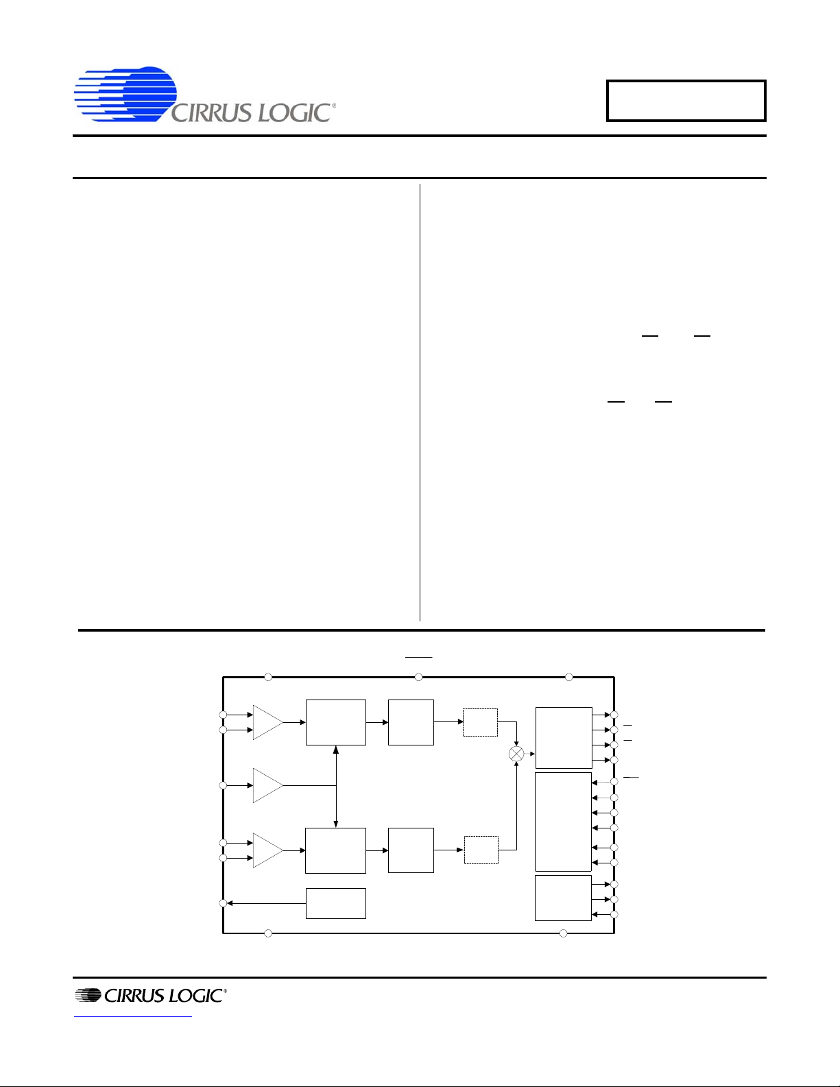
4. THEORY OF OPERATION ..................................................................................................... 10
4.1 Digital Filters .......................... .......................................... ................................................10
4.2 Active Power Computation ............................... ... .... ... ... ... .... ... ... ... ... .... ... .........................10
5. FUNCTIONAL DESCRIPTION ............................................................................................... 11
5.1 Analog Inputs ................ ... .......................................... ... ... .... ............................................ 11
5.1.1 Voltage Channel ..................... ... .... ... ... .......................................... ... .... ... ... ... ......11
5.1.2 Current Channel ............................... ... ... .... ... ... ... .......................................... ... ... 11
5.2 High-pass Filter ... .............................................................................................................11
5.3 Energy Pulse Outputs ......... .......................................... ... .... ......................................... ... 11
5.3.1 Pulse Output Format. ....................................... ... .... ......................................... ... 11
5.3.2 Selecting Frequency of E1 and E2 ...................... .... ... ... ... ... .... ... ... ... .... ... ............11
5.3.3 Selecting Frequency of FOUT ............................................................................. 12
5.3.4 Absolute Max Frequency on E1 and E2 ..............................................................12
5.3.5 E1 and E2 Frequency Calculation .......................................................................13
5.4 Energy Direction Indicator ............ ... ... ... .... ... ... ... .......................................... ...................13
5.5 Power-on Reset ............................ ... ... .......................................... ... .... ............................13
5.6 Oscillator Characteristics .................... ... .... ... ... ... .... ... ... .......................................... ... ... ...13
5.7 Basic Application Circuit ..................................................................................................14
6. PACKAGE DIMENSIONS ....................................................................................................... 15
7. REVISION HISTORY .............................................................................................................. 16
CS5466
LIST OF FIGURES
Figure 1. Timing Diagram for E1, E2 and FOUT (Not to Scale)...................................................... 8
Figure 2. Data Flow....................................................................................................................... 10
Figure 3. Oscillator Connection.....................................................................................................13
Figure 4. Typical Connection Diagram..........................................................................................14
LIST OF TABLES
Table 1. Current Channel PGA Setting .........................................................................................11
Table 2. Maximum Frequency for E1, E2, and FOUT................................................................... 12
Table 3. Absolute Max Frequency on E1 and E2..........................................................................12
2 DS659F2
Page 3

CS5466
1. OVERVIEW
The CS5466 is a CMOS monolithic power measurement device with an energy computation engine. The CS5466
combines a programmable gain am plifier, two ADCs, and energy-to-frequency conversion circuitry on a single
chip.
The CS5466 is designed for energy measurement applications and is optimized to interface to a shunt or current
transformer for current measurement, and to a resistive divider or transformer for voltage measurement. The curre nt
channel has a programmable gain amplifier (PGA) which provides four full-scale input options. With a single +5 V
supply on VA+/AGND, both of the CS5466’s input channels accommodate common-mode plus signal levels between (AGND - 0.25 V) and VA+.
The CS5466 has three pulse output pins: E1
counter or stepper motor, or interface to a microcon troller. The FOUT pi n conveys active (real) po wer at a pulse frequency many times higher than that of the E1
, E2, and FOUT. E1 and E2 can be used to directly drive a mechanica l
or E2 pulse frequency, allowing for high-speed calibration.
DS659F2 3
Page 4
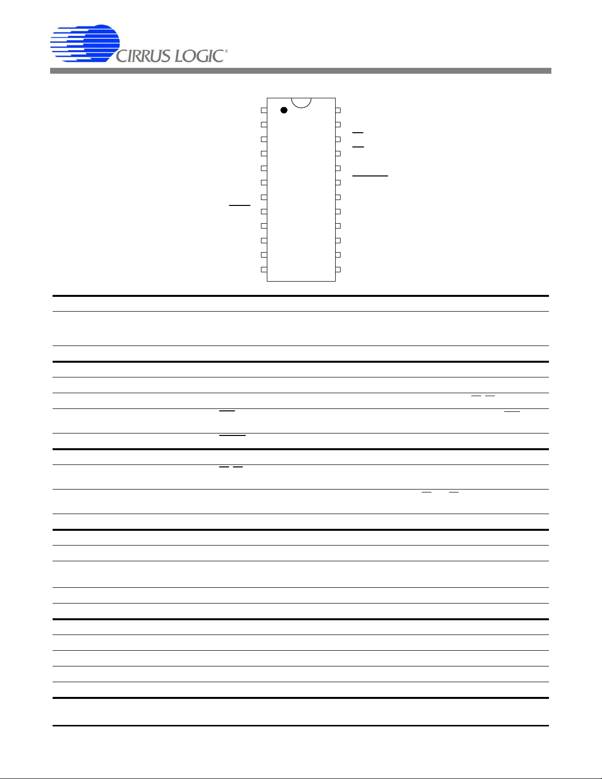
CS5466
VREFIN 12Voltage Reference Input
VREFOUT 11Voltage Reference Out put
VIN- 10Differential Voltage I nput
VIN+ 9Differential Voltage I nput
HPF 8High-pass Filter Ena ble
IGAIN1 7Gain Select 1
NEG 6Negative Energy In di c at or
IGAIN0 5Gain Select 0
DGND 4Digital Ground
VD+ 3Positive Power Supply
CPUCLK 2CPU Clock Out put
XOUT 1Crystal Out
AGND13 Analog G round
VA+14 Positive Anal og S uppl y
IIN-15 Dif ferential Cur r ent I nput
IIN+16 Dif ferential Cur r ent I nput
FREQ217 Frequency Select 2
FOUT18 High-f r equenc y Output
RESET19 Reset
FREQ120 Frequency Select 1
E221 Energy Outpu t 2
E122 Energy Outpu t 1
FREQ023 Frequency Select 0
XIN24 Crystal In
2. PIN DESCRIPTION
Clock Generator
Crystal Out
Crystal In
CPU Clock Output 2
Control Pins
Gain Select 5, 7
Frequency Select 17, 20, 23
High Pass Filter Enable 8
Reset 19
Energy Pulse Outputs
Energy Output 22, 21
High Freq Output 18
Neg Energy Indicator 6
Analog Inputs/Outputs
Differential V ol tage Inputs 9, 10
Voltage Reference
Output
Voltage Reference Input 12
Differential Current Inputs 16, 15
Power Supply Connections
Positive Digital Supply 3
Digital Ground 4
Analog Ground 13
Positive Analog Supply 14
1, 24
11
4 DS659F2
XOUT , X IN - A single stage amplifier inside the chip is connected to these pins and can be used
with a crystal to provide the system clock for the device. Alternatively, an external clock can be
supplied to the XIN pin to provide the system clock for the device.
CPUCLK - Output of on-chip oscillator which can drive one standard CMOS load.
IGAIN1, IGAIN0 - Used to select the current channel input gain range.
FREQ2,FREQ1,FREQ0 - Used to select max pulse output frequency for E1, E2, and FOUT.
HPF - High disables the HPF. Low activates HPF on Voltage channel. Connecting HPF pin to
FOUT pin activates HPF on Current channel.
RESET - Low activates Reset.
E1, E2 - Active low alternating pulses with an output frequency that is proportional to the active
(real) power.
FOUT - Outputs energy pulses at a frequency higher than E1 and E2 outputs. Used for calibra-
tion purposes.
NEG - High indicates negative energy.
VIN+, VIN- - Differential analog input pins for voltage channel.
VREFOUT - The on-chip voltage reference output pin. The voltage reference has a nominal
magnitude of 2.5 V and is referenced to the AGND pin on the converter.
VREFIN - Voltage input to this pin establishes the voltage reference for the on-chip modulators.
IIN+, IIN- - Differential analog input pins for current channel.
VD+ - The positive digital supply.
DGND - Digital Ground.
AGND - Analog Ground.
VA+ - The positive analog supply.
Page 5
CS5466
3. CHARACTERISTICS & SPECIFICATIONS
RECOMMENDED OPERATING CONDITIONS
Parameter Symbol Min Typ Max Unit
Positive Digital Power Supply VD+ 3.135 5.0 5.25 V
Positive Analog Power Supply VA+ 4.75 5.0 5.25 V
Voltage Reference VREFIN - 2.5 - V
Specified Temperature Range T
A
ANALOG CHARACTERISTICS
• Min / Max characteristics and specifications are guaranteed over all operating ponditions.
• Typical characteristics and specifications are measured at nominal supply voltages and TA = 25 °C.
• VA+ = 5 V ±5% VD+ = 3.3 V ±5% or 5 V ±5%; AGND = DGND = 0 V. All voltages with respect to 0 V.
• MCLK = 4.096 MHz
Parameter Symbol Min Typ Max Unit
Analog Inputs (Current Channel)
Differential Input Range (Gain = 10)
[(I
IN+)-(IIN-)] (Gain = 50)
(Gain = 100)
(Gain = 150)
Input Capacitance (All Gain Ranges) C
Effective Input Impedance (All Gain Ranges) Z
Analog Inputs (Voltage Channel)
Differential Input Range [(V
IN+)-(VIN-)] VIN --±250mV
Input Capacitance C
Effective Input Impedance Z
Accuracy (Energy Outputs)
Active Energy Linearity All Gain ranges
(Note 1) Input Range 0.1% - 100% - - ±0.1 - %
Full-scale Error (Note 2) - - 4.0 - %FS
Offset Error (Note 2) - - 0.06 - %FS
I
IN -
inI -25-pF
inI 30 - - k
inV -0.2-pF
inV 2--M
-40 - +85 °C
±250
-
-
-
±50
±25
±16.7
-
-
-
-
mV
mV
mV
mV
Notes: 1. Applies when the HPF option is enabled
2. Applies before system calibration. Specified as a percentage of full scale (FS).
DS659F2 5
Page 6

ANALOG CHARACTERISTICS (Continued)
PSRR 20
0.150V
V
eq
----------------- -
log=
(VREFOUTMAX - VREFOUTMIN)
VREFOUT
AVG
(
(
1
T
A
MAX
- T
A
MIN
(
(
1.0 x 10
(
(
6
TC
VREF
=
Parameter Symbol Min Typ Max Unit
Power Supplies
Power Supply Currents I
I
(VA+ = VD+ = 5 V)
D+
(VA+ = 5 V, VD+ = 3.3 V)
I
D+
Power Consumption (VA+ = VD+ = 5 V)
(Note 3) (VA+ = 5 V, VD+ = 3.3 V)
Power Supply Rejection Ratio (50, 60 Hz)
(Note 4) Voltage Channel (Gain = 10)
Current Channel (All Gains)
A+
-
-
-
-
-
PSRR 45
56
CS5466
-
-
-
-
-
1.3
2.9
1.7
21
11.6
55
75
25
-
-
-
-
-
-
-
mA
mA
mA
mW
mW
dB
dB
Notes:
3. All outputs unloaded. All inputs CMOS level.
4. Definition for PSRR: VREFIN tied to VREFOUT, VA+ = VD+ = 5 V, a 150 mV zero-to-peak sine wave (frequency =
60 Hz) is imposed onto the +5 V supply voltage at VA+ and VD+ pins. The “+” and “-” input pins of both input
channels are shorted to VA-. Then the CS5466 is put into an internal test mode and digital output data is collected
for the channel under test. The zero-peak value of the digital sinusoidal output signal is determined, and this value
is converted into the zero-peak value of the sinusoidal voltage that would need to be applied at the channel’s inputs,
in order to cause the same digital sinusoidal output. This voltage is then defined as Veq. PSRR is then (in dB):
VOLTAGE REFERENCE
Parameter Symbol Min Typ Max Unit
Reference Output
Output Voltage REFOUT + 2.4 +2.5 +2.6 V
VREFOUT Temperature Coefficient (Note 5) TC
Load Regulation (Note 6) V
Reference Input
Input Voltage Range VREFIN - +2.5 - V
Input Capacitance - - 4 - pF
Input CVF Current - - 70 - nA
Notes: 5. The voltage at VREFOUT is measured across the temperature range. From these measurements the following
formula is used to calculate the VREFOUT Temperature Coefficient
VREF - 25 60 ppm/°C
R
-610mV
:.
6. Specified at maximum recommended output current of 1 A, source or sink.
6 DS659F2
Page 7

CS5466
DIGITAL CHARACTERISTICS (Note 7)
• Min / Max characteristics and specifications are guaranteed over all operating conditions.
• Typical characteristics and specifications are measured at nominal supply voltages and TA = 25 °C.
• VA+ = 5 V ±5% VD+ = 3.3 V ±5% or 5 V ±5%; AGND = DGND = 0 V. All voltages with respect to 0 V.
• MCLK = 4.096 MHz
Parameter Symbol Min Typ Max Unit
Master Clock Characteristics
Master Clock Frequency Internal Gate Oscillator MCLK 3 4.096 5 MHz
Master Clock Duty Cycle - 40 - 60 %
CPUCLK Duty Cycle (Note 8 and 9) - 40 - 60 %
Filter Characteristics
High-pass Filter Corner Frequency -3 dB - - 0.125 - Hz
Input/Output Characteristics
High-level Input Voltage
XIN
RESET
Low-level Input Voltage (VD = 5 V)
XIN
RESET
Low-level Input Voltage (VD = 3.3 V)
XIN
RESET
High-level Output Voltage (except XOUT) I
Low-level Output Voltage (except XOUT) I
= +5 mA V
out
= -5 mA V
out
Input Leakage Current I
Digital Output Pin Capacitance C
Drive Current FOUT, E1
, E2, NEG (Note 10) I
V
V
V
OH
OL
in
out
DR
IH
IL
IL
(VD+) - 0.5
0.8VD+
-
-
-
-
-
-
-
-
-
-
-
-
1.5
0.2VD+
0.3
0.2VD+
V
V
V
V
V
V
(VD+) - 1.0 - - V
--0.4V
-±1±10µA
-5-pF
-50-mA
Notes: 7. All measurements performed under static conditions.
8. If external MCLK is used, then the duty cycle must be between 45% and 55% to maintain this specification.
9. The frequency of CPUCLK is equal to MCLK.
10. V
and VOH are not specified under this condition.
OL
DS659F2 7
Page 8

SWITCHING CHARACTERISTICS
E1
E2
FOUT
t
1
t
2
t
3
t
5
t
6
t
4
t
7
t
3
t
1
t
2
Figure 1. Timing Diagram for E1, E2 and FOUT (Not to Scale)
• Min / Max characteristics and specifications are guaranteed over all operating conditions.
• Typical characteristics and specifications are measured at nominal supply voltages and TA = 25 °C.
• VA+ = 5 V ±5% VD+ = 3.3 V ±5% or 5 V ±5%; AGND = DGND = 0 V. All voltages with respect to 0 V.
• Logic Levels: Logic 0 = 0 V, Logic 1 = VD+.
Parameter Symbol Min Typ Max Unit
Rise Times Digital Output (Note 11) t
Fall Times Digital Output (Note 11) t
rise
fall
Start-up
Oscillator Start-up Time XTAL = 4.096 MHz (Note 12) t
and E2 Timing (Note 13 and 14)
E1
Period t
Pulse Width t
Rising Edge to Falling Edge t
Falling Edge to E2 Falling Edge t
E1
ost
1
2
3
4
FOUT Timing (Note 13 and 14)
Period t
Pulse Width (Note 15) t
FOUT Low t
5
6
7
Notes: 11. Specified using 10% and 90% points on wave-form of interest. Output loaded with 50 pF.
12. Oscillator start-up time varies with crystal parameters. This specification does not apply when using an external
clock source.
13. Pulse output timing is specified at MCLK = 4.096 MHz. Current and voltage signals are at unity power factor. See
”Energy Pulse Outputs” on page 11. for more information on pulse output pins.
14. Timing is proportional to the frequency of MCLK.
15. When FREQ2 = 0, FREQ1=1 and FREQ0=1, FOUT will have a typical pulse width of 20 s at MCLK = 4.096 MHz.
-50-ns
-50-ns
-60-ms
500 - - ms
250 - - ms
250 - - ms
250 - - ms
0.10 1 / f
FOUT
-0.5*t590 ms
-0.5*t5-ms
CS5466
ms
8 DS659F2
Page 9

ABSOLUTE MAXIMUM RATINGS
WARNING: Operation at or beyond these limits may result in permanent damage to the device.
Normal operation is not guaranteed at these extremes
Parameter Symbol Min Typ Max Unit
DC Power Supplies (Notes 16 and 17)
Positive Digital
Positive Analog
Input Current, Any Pin Except Supplies (Notes 18, 19, 20) I
Output Current, Any Pin Except VREFOUT I
Power Dissipation (Note 21) P
Analog Input Voltage All Analog Pins V
Digital Input Voltage All Digital Pins V
Ambient Operating Temperature T
Storage Temperature T
Notes: 16. VA+ and AGND must satisfy {(VA+) - (AGND)} + 6.0 V.
17. VD+ and AGND must satisfy {(VD+) - (AGND)} + 6.0 V.
18. Applies to all pins including continuous over-voltage conditions at the analog input pins.
19. Transient current of up to 100 mA will not cause SCR latch-up.
20. Maximum DC input current for a power supply pin is ±50 mA.
21. Total power dissipation, including all input currents and output currents.
.
VD+
VA+
IN
OUT
D --500mW
INA
IND
A
stg
-0.3
-0.3
-
-
--±10mA
--100mA
- 0.3 - (VA+) + 0.3 V
-0.3 - (VD+) + 0.3 V
-40 - 85 °C
-65 - 150 °C
CS5466
+6.0
+6.0
V
V
DS659F2 9
Page 10

4. THEORY OF OPERATION
2nd Order
Modulator
4th Order
Modulator
x
VIN±
IIN±
Energy-toPulse Rate
Converter
E1
E2
FOUT
Sinc
3
PGA
10x
HPF
NEG
IGAIN[1:0]
FREQ[2:0]
IIR
IIR
Sinc
3
Current Channel
Voltage Channel
Digital Filter
HPF
N=400
N
HPF
Config
Digital Filter
Figure 2. Data Flow
CS5466
The CS5466 is a dual-channel analog-to- digital converter (ADC) followed by a computation engine that performs an energy-to-pulse conversion. The flow diagram
for the two data paths is depicted in Figure 2. The analog inputs are structured with two dedicated channels,
voltage and current, then optimized to simplify interfacing to sensing elements.
the IIR filter to compensate for the magnitude roll-off of
the low-pass filtering operation.
An optional digital high-pass filter (HPF in Figure 2) removes any DC component from the selected signal
path. By removing the DC component from the voltage
or current channel, any DC content will also be removed
from the calculated average active (real) power as well.
The voltage-sensing element introduces a voltage
waveform on the voltage channel input VIN and is subject to a fixed 10x gain amplifier. A second-order deltasigma modulator samples the amplified signal for digitization.
Simultaneously, the current sensing element introduces
a voltage waveform on the current channel input IIN
and is subject to four programmable gains. The amplified signal is sampled by a fourth-order delta-sigma
modulator for digitization. Both converters sample at a
rate of MCLK / 8. The over-sampling provides a wide
dynamic range and simplified anti-alias filter design.
4.2 Active Power Computation
The instantaneous voltage and current data samples
are multiplied to obtain the instantaneous power. The
product is then averaged over 400 conversions to com-
pute the active power value used to drive pulse outputs
E1
, E2, and FOUT. Output pulse rate of E1 and E2 can
be set to one of four frequencies to directly drive a stepper motor or a electromechanical counter or inte rface to
a microcontroller or infrared LED. The alternating output
pulses of E1
tromechanical counters.
and E2 allows for use with low-cost elec-
Output FOUT provides a uniform pulse stream that is
4.1 Digital Filters
The decimating digital filters on both channels a re Sinc
filters followed by fourth-order IIR filters. The single-bit
data is passed to the low-pass decimation filter and out-
proportional to the active power and is designed for sys-
3
tem calibration. The FREQ[2:0] inputs set the output
pulse rate of E1
, E2, and FOUT. See ”Energy Pulse
Outputs” on page 11. for more details.
put at a fixed word rate. The o utput word is passed to
10 DS659F2
Page 11

CS5466
250mV
P
2
-----------------
176.78mV
RMS
5. FUNCTIONAL DESCRIPTION
5.1 Analog Inputs
The CS5466 is equipped with two fully differential input
channels. The inputs VIN and IIN are designated as
the voltage and current channel inputs, respectively.
The full-scale differential input voltage for the current
and voltage channel is 250 mV
5.1.1 Voltage Channel
The output of the line-voltage resistive divider or transformer is connected to the VIN+ and VIN- input pins of
the CS5466. The voltage channel is equipped with a
10x, fixed-gain amplifier. The full-scale signal level that
can be applied to the voltage channel is 250 mV. If the
input signal is a sine wave, the maximum RMS voltage
is:
which is approximately 70.7% of maximum peak voltage.
5.1.2 Current Channel
The output of the current-sense resistor or transformer
is connected to the IIN+ and IIN- input pins of the
CS5466. To accommodate different current-sensing devices, the current channel incorporates programmable
gains which can be set to one of four input ra nges. Input
pins IGAIN1 and IGAIN0 (See Table 1) define the four
gain selections and corresponding maximum input signal level.
IGAIN1 IGAIN0 Maximum Input
0 0 ±250mV 10x
01±50mV50x
1 0 ±25mV 100x
1 1 ±16.67mV 150x
Table 1. Current Channel PGA Setting
For example, if IGAIN1=IGAIN0=0, the current channel’s gain is set to 10x. If the input signals are pu re sinusoids with zero phase shift, the maximum peak
differential signal on the current or voltage channel is
250 mV
70.7% of maximum peak voltage producing a full-scale
energy pulse registration equal to 50% of absolute maximum energy pulse registration. This will be discussed
further in Section 5.3 Energy Pulse Outputs on page 11.
. The input signal levels are approximately
P
.
P
Range
5.2 High-pass Filter
By removing the offset from either channel, no error
component will be generated at DC when computing the
active power. Input pin HPF
– High-pass Filter (HPF) is disabled when pin HPF is
connected high.
– HPF is enabled in the voltage channel when pin HPF
connected low.
– HPF is enabled in the current channel when pin HPF is
connected to pin FOUT.
defines the three options:
is
5.3 Energy Pul s e Outputs
The CS5466 provides three output pins for energy registration. The E1
from which energy can be r egistered. These pins are
designed to directly connect to a stepper m otor or electromechanical counter. The pulse rate on the E1
pins are in the range of 0 to 4 Hz and all frequency settings are optimized to be used with standard meter constants. The FOUT pin is designated for system
calibration and the pulse rate can be selected to reach
a frequency of 8000 Hz.
and E2 pins provide a simple interface
and E2
5.3.1 Pulse Output Format.
The CS5466 produces alternating pulses on E1 an d E2.
This pulse format is designed to drive a stepper motor.
Each pin produces active-low pulses with a minimum
pulse width of 250 ms when MCLK = 4.096 MHz. Refer
to “Switching Characteristics” on page 8 for timing parameters.
The FOUT pin issues active-high pulses. The pulse
width is equal to 90 ms (typical), unless the period falls
below 180 ms. At this time the pulses will be equal to
half the period. In mode 3 (FREQ[ 2:0] = 3), th e pulse
width of all FOUT pulses is typically 20 s regardless of
the pulse rate (MCLK = 4.096 MHz).
5.3.2 Selecting Frequency of E1 and E2
The pulse rate on E1 and E2 can be set to one of four
frequency ranges. Input pins FREQ1 and FREQ0 (See
Table 2) determine the maximum frequency on E1
E2
for pure sinusoidal inputs with zero phase shift. As
shown in Figure 1 on page 8, the frequency of E2
equal to the frequency of E1
pulses.
As discussed in Section 5.1.2 Current Channel on page
11, the maximum frequency on the E1
pins is equal to the selected frequency in Table 2 if the
maximum peak differential signal applied to both channels is a sine wave with zero phase shift.
with active-low alternating
and E2 output
and
is
DS659F2 11
Page 12

CS5466
Frequency Select Maximum Frequency for a Sine Wave (Notes 1, 2 and 3)
FREQ2 FREQ1 FREQ0 E1
0 0 0 0.125 Hz 0.25 Hz 64x(E1
0 0 1 0.25 Hz 0.5 Hz 32x(E1
0 1 0 0.5Hz 1.0 Hz 16x(E1
0 1 1 1.0 Hz 2.0 Hz 2048x(E1
1 0 0 0.125 Hz 0.25 Hz 128x(E1
1 0 1 0.25 Hz 0.5 Hz 64x(E1
1 1 0 0.5 Hz 1.0 Hz 32x(E1
1 1 1 1.0 Hz 2.0 Hz 16x(E1
Notes: 1 A pure sinusoidal input with zero phase shift is applied to the voltage and current channel.
2 MCLK = 4.096 MHz
3 See Figure 1 on page 8 for E1 and E2 timing diagram.
Table 2. Maximum Frequency for E1, E2, and FOUT
5.3.3 Selecting Frequency of FOUT
The pulse output FOUT is designed to assist with meter
calibration. Using the FREQ[2:0] pins, FOUT can be set
to frequencies higher than that of E1
frequency is directly proportional to the E1
quencies. Table 2 defines the maximum frequencies for
FOUT and the dependency of FOUT on E1
and E2. The FOUT
5.3.4 Absolute Max Frequency on E1
or E2 E1+E2 FOUT
The absolute maximum pulse rate observed on E1
E2
, determined by the FREQ[2:0] selection is defined
below in Table 3.
and E2 fre and E2.
Frequency Select Absolute Max Frequency
FREQ2 FREQ1 FREQ0 E1
x 0 0 0.25 Hz 0.5 Hz
and E2
The CS5466 supports input signals on the voltage and
current channels that may not be a sine wave. A typical
situation of achieving the absolute maximum frequency
on E1
and E2 would be if a 250 mV dc signal is applied
to the VIN and IIN input pins. The digital high-pass filter
should be disengaged by selecting HPF
= 1.
x 0 1 0.5 Hz 1.0 Hz
x 1 0 1.0 Hz 2.0 Hz
x 1 1 2.0 Hz 4.0 Hz
Table 3. Absolute Max Frequency on E1
+E2)16 Hz
+E2)16 Hz
+E2)16 Hz
+E2) 4,096 Hz
+E2)32 Hz
+E2)32 Hz
+E2)32 Hz
+E2)32 Hz
and
or E2 E1+E2
and E2
12 DS659F2
Page 13

CS5466
FREQ
E1,E2
= Actual frequency of E1 and E2 pulses [Hz]
VIN = rms voltage across VIN+ and VIN- [V]
IIN = rms voltage across IIN+ and IIN- [V]
IGAIN = Current channel gain selection (10, 50, 100, 150)
PF = Power Factor
FREQ
max
= Absolute Max Frequency for E1 and E2 [Hz]
VREFIN = Voltage at VREFIN pin [V]
FREQ
E1,E2
VIN 10 IIN IGAIN PF FREQ
max
VREFIN
2
------------------------------------------------------------------------------------------------------------------
=
0.25Vp10 0.025V
p
100 1 2Hz
22 2.5V
2
-------------------------------------------------------------------------------------------------------- -
1Hz=
FOUT 2048 E1 E2+ 2048 2Hz 4096Hz===
Oscillator
Circuit
DGND
XIN
XOUT
C1
C1 = 22 pF
C2
C2 =
Figure 3. Oscillator Connection
5.3.5 E1 and E2 Frequency Calculation
The pulse output frequency of E1 and E2 is directly proportional to the active power calculated from the input
signals. To calculate the output frequency on E1
E2
, use the following transfer function:
Example:
For a given application, assume a 50 Hz line frequency
and a purely resistive load (unity power factor), the following configuration is used:
– FREQ[2:0] = 3 FREQ
max
= 2 Hz
– IGAIN[1:0] = 2 IGAIN = 100
– VREFIN = VREFOUT = 2.5 V
In this configuration, the maximum sine wave that can
be applied is 250 mVp on the voltage channel and
25 mVp on the current channel. Using the above equation, the output frequency of energy pulse E1
calculated:
and
or E2 is
output pin will become active-high and will remain active-high until positive active power is detected. The
NEG pin is valid at least 250ns prior to any assertion of
E1
or E2, and FOUT, to indicate the sign of a given energy output. The NEG pin is updated at a rate of 10 Hz
at MCLK = 4.096 MHz.
5.5 Power-on Reset
Upon powering up, the digital circuitry is held in reset
until the analog voltage reaches 4.0 V. At that time, an
eight-XIN-clock-period delay is enabled to allow the oscillator to stabilize. The CS5466 will then initialize. The
device reads the control pins IGAIN[1:0], FREQ[2:0]
and HPF
, and begins performing energy measure-
ments.
5.6 Oscillator Characteristics
XIN and XOUT are the input and output of an inverting
amplifier which can be configured as an on-chip oscillator, as shown in Figure 3. The oscillator circuit is designed to work with a quartz crystal. To reduce circuit
With maximum pure sinusoidal input signals, the frequency of E1
or E2 is half the absolute maximum fre-
quency set with FREQ[2:0].
To calculate the frequency of FOUT for the example
above, assume FREQ2 = 0.
5.4 Energy Direction Indicator
The NEG pin indicates the sign of the calculated active
power. If negative active power is detected, the NEG
DS659F2 13
cost, two load capacitors C1 and C2 are integrated in
the device, one between XIN and DGND and the other
between XOUT and DGND. Lead lengths to/from the
crystal should be minimized to reduce stray capacitance. To drive the device from an external clock
source, XOUT should be left unconnected while XIN is
driven by the external circuitry. There is an amplifier between XIN and the digital section which provides
CMOS-level signals. This amplifier works with sinusoidal inputs so there are no problems with slow edge
times.
Page 14

CS5466
EDIR / P4
VD+
FOUT
XOUT
XIN
CPUCLK
DGNDVA-
VREFOUT
VREFIN
IIN+
IIN-
VIN-
VIN+
AGND
3
15
14
9
10
16
12
11
13 4
2
24
1
18
22
21
120 VAC
10500500
470 nF
470 F0.1
F
0.1F
R
SHUNT
0.1 F
R
1
NL
AGND
VA+
E2
E1
R
I+
R
I-
R
V-
C
Idiff
C
Vdiff
C
V-
C
V+
C
I+
C
I-
FREQ2
17
FREQ1
20
FREQ0
23
IGAIN1
7
IGAIN0
5
NEG
6
IHPF
8
Stepper
Motor
5466
Config.
Settings
4.096 MHz
10 k
1
F
RESET
Calibratio
n
Resistor
Note:
Indicates common (floating) return.
R
2
19
Figure 4. Typical Connection Diagram
5.7 Basic Application Circuit
Figure 4 shows the CS5466 configured to measure
power in a single-phase, 2-wire syste m while op erat ing
in a single-supply configuration. In this diagram, a shunt
resistor is used to sense the line current and a voltage
divider is used to sense the lin e voltage. In this type of
shunt resistor configuration, the common-mode level of
the CS5466 must be referenced to the line side of the
power line. This means that the common-mode potential of the CS5466 will track the high voltage levels, as
well as low voltage levels, with respect to earth ground
potential.
14 DS659F2
Page 15

6. PACKAGE DIMENSIONS
24L SSOP PACKAGE DRAWING
E
N
1
23
e
b
2
A1
A2
A
D
SEATING
PLANE
E1
1
L
SIDE VIEW
END VIEW
TOP VIEW
INCHES MILLIMETERS NOTE
DIM MIN NOM MAX MIN NOM MAX
A -- -- 0.084 -- -- 2.13
A1 0.002 0.006 0.010 0.05 0.13 0.25
A2 0.064 0.068 0.074 1.62 1.73 1.88
b 0.009 -- 0.015 0.22 -- 0.38 2,3
D 0.311 0.323 0.335 7.90 8.20 8.50 1
E 0.291 0.307 0.323 7.40 7.80 8.20
E1 0.197 0.209 0.220 5.00 5.30 5.60 1
e 0.022 0.026 0.030 0.55 0.65 0.75
L 0.025 0.03 0.041 0.63 0.75 1.03
0° 4° 8° 0° 4° 8°
CS5466
JEDEC #: MO-150
Controlling Dimension is Millimeters.
Notes: 1. “D” and “E1” are reference datums and do not included mold flash or protrusions, but do include mold
mismatch and are measured at the parting line, mold flash or protrusions shall not exceed 0.20 mm per
side.
2. Dimension “b” does not include dambar protrusion/intrusion. Allowable dambar protrusion shall be
0.13 mm total in excess of “b” dimension at maximum material condition. Dambar intrusion shall not
reduce dimension “b” by more than 0.07 mm at least material condition.
3. These dimensions apply to the flat section of the lead between 0.10 and 0.25 mm from lead tips.
DS659F2 15
Page 16

CS5466
Contacting Cirrus Logic Support
For all product questions and inquiries contact a Cirrus Logic Sales Representative.
To find the one nearest to you go to www.cirrus.com
IMPORTANT NOTICE
Cirrus Logic, Inc. and it s subs i dia ri e s (“Ci rr u s”) bel i eve tha t the in for mat i on c ont ai ned i n t his doc ument i s acc urate and reliable. Howev er, t he in f ormation is subject
to change without not ice and is provi ded “AS IS” wit hout warr anty of any kind (expres s or impl ied). Customers a re advi sed to o btain the latest version of relevant
information to verify, before placing or ders, tha t inform ation being relied on is curr ent and com plete. Al l prod ucts are so ld subject to the terms and conditions o f sale
supplied at the time of order acknowledgment, including those pertaining to warranty, indemnification, and limitation of liability. No responsibility is assumed by Cirrus
for the use of this information, including use of this informat ion as the basis for ma nufacture or sale of any items, or for in fringe ment of patents or oth er rights of third
parties. This document is the proper ty of Ci rru s and by furnishing this information, Cirrus grants no license, express or implied under any patents, mask work rights,
copyrights, trademarks, trade secrets or other intell ectual prop erty rights. Cirrus owns the cop yrights associated with the information contained herein a nd gives con sent for copies to be made of the information only for use within your organization with respect to Cirrus integrated circuits or other products of Cirrus. This consent
does not extend to other copying such as copying for ge ne ral distribution, advertising or promotional purposes, or for creating any work for resale.
CERTAIN APPLICATIONS USING SEMICONDUCTOR PRODUCTS MAY INVOLVE POTENTIAL RISKS OF DEATH, PERSONAL INJURY, OR SEVERE PROPERTY OR ENVIRONMENTAL DAMAGE (“CRITICAL APPLICATIONS”). CIRRUS PRODUCTS ARE NOT DESIGNED, AUTHORIZED O R WARRAN TED FOR USE
IN PRODUCTS SURGICALLY IMPLANTED INTO THE BODY, AUTOMOTIVE SAFETY OR SECURITY DEVICES, LIFE SUPPORT PRODUCTS OR OTHER CRITICAL APPLICATIONS. INCLUSION OF CIRRUS PRODUCTS IN SUCH APPLICATIONS IS UNDERSTOOD TO BE FULLY AT THE CUSTOMER'S RISK AND CIRRUS DISCLAIMS AND MAKES NO WARRANTY, EXPRESS, STATUTORY OR IMPLIED, INCLUDING THE IMPLIED WARRANTIES OF MERCHANTABILITY AND
FITNESS FOR PARTICULAR PURPOSE, WITH REGARD TO ANY CIRRUS PRODUCT THAT IS USED IN SUCH A MANNER. IF THE CUSTOMER OR CUSTOMER'S CUSTOMER USES OR PERMITS THE USE OF CIRRUS PRODUCTS IN CRITICAL APPLICATIONS, CUSTOMER AGREES, BY SUCH USE, TO FULLY
INDEMNIFY CIRRUS, ITS OFFICERS, DIRECTORS, EMPLOYEES, DISTRIBUTORS AND OTHER AGENTS FROM ANY AND ALL LI ABI LITY, INCLUDI NG ATTORNEYS' FEES AND COSTS, THAT MAY RESULT FROM OR ARISE IN CONNECTION WITH THESE USES.
Cirrus Logic, Cirrus, and the Cirrus Logic logo designs are trademarks of Cirrus Logic, Inc. All other brand and pr oduct names in this document may be trademarks
or service marks of their respective owners.
7. ORDERING INFORMATION
Model Temperature Package
CS5466-ISZ (lead free) -40 to +85 °C 24-pin SSOP
8. ENVIRONMENTAL, MANUFACTURING, & HANDLING INFORMATION
Model Number Peak Reflow Temp MSL Rating* Max Floor Life
CS5466-ISZ (lead free) 260 °C 3 7 Days
* MSL (Moisture Sensitivity Level) as specified by IPC/JEDEC J-STD-020.
9. REVISION HISTORY
Revision Date Changes
PP1 SEP 2004 Initial Release
PP2 OCT 2004 Corrected table heading on Page 6.
PP3 JUN 2005 Minor edits
F1 AUG 2005
F2 APR 2011 Removed lead-containing (Pb) device ordering information.
Updated with most-current characterization data. corrected energy pulse output
rate equation on p13. Added MSL data.
16 DS659F2
 Loading...