

CS5396
CS5397
120 dB, 96 kHz Audio A/D Converter
Features
l 24-Bit Conversion
l 120 dB Dynamic Range (A-Weighted)
l Low Noise and Distortion
>105 dB THD + N
l Complete CMOS Stereo A/D System
Delta-Sigma A/D Converters
Digital Anti-Alias Filtering
S/H Circuitry and Voltage Reference
l CS5396 - digita l filter optimized for audio
l CS5397 - non-aliasing digital filter
l Adjustable System Sampling Rates
including 32, 44.1, 48 & 96 kHz
l Differential Analog Architecture
l Linear Phase Digital Anti-Alias Filtering
l 10 Tap Programmable Psychoacoustic Noise
Shaping Filter
l Single +5 V Power Supply
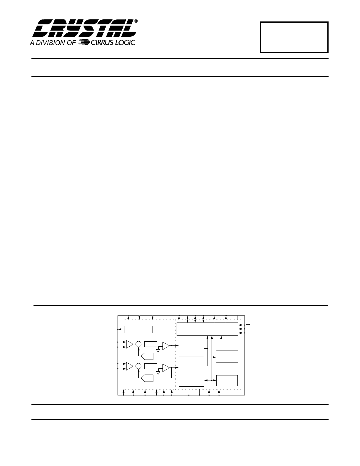
General Description
The CS5396 and CS5397 are complete analog-to-digital
converters for stereo digital audio systems. They perform sampling, analog-to-digital conversion and antialias filtering, gener ating 24-bit values for both left and
right inputs in ser ial form a t sa mple rate s up to 1 00 kHz
per channel.
The CS5396/97 use a patented 7th-order, tri-level deltasigma modulator followed by digital filtering and decimation, which removes the need for an external anti-alias
filter. The ADCs use a differential architecture which provides excellent noise rejection.
The CS5396 has a linear phase filter optimized for audio
applications with ±0.005 dB passband ripple and
>117 dB stopband rejection. The CS5397 has a nonaliasing filter respo nse with ±0.005 passband rippl e an d
>117 dB stopband attenuation. Other fea tures a vail able
in both the CS5396 and CS5397 are an optional low
group delay filter and a unique psychoacoustic noise
shaping filter which s ubjectively truncates the output to
16, 18 or 20 bits while 24-bit sound quality is preserved.
The CS5396/97 are targeted for the highest performance professional audio systems requiring wide
dynamic range, negligible distortion and low noise.
VCOM MCLKA LRCKADCTL
VREF
AINL-
AINL+
AINR-
AINR+
Voltage Referen ce
S/H
S/H
VA
AGND1 AGND2 AGND0 VL TST1 VD DGND
Preliminary Product Information
Cirrus Logic, Inc.
Crystal Semiconductor Products Division
P.O. Box 17847, Austin, Texas 78760
(512) 445 7222 FAX: (512) 445 7581
http://www.crystal.com
ORDERING INFORMATION
CS5396-KS -10° to 50° C 28-pin SOIC
CS5397-KS -10° to 50° C 28-pin SOIC
CDB5396/97 Evaluation Board
SCLK SDAT A1 MCLKD
DACTL
CAL SDAT A2
CS
Serial Output Interface
+
LP Filter
-
+
-
DAC
LP Filter
DAC
Comparator
Comparator
+
-
+
-
LGND TST0
Digital Decimation
Filter
(with Low Group
Delay Options)
Digital Decimation
Filter
(with Low Group
Delay Options)
Calibration
Microcontroller
This document contains information for a new product.
Cirrus Logic reserves the right to modify this product without notice.
Copyright Cirrus Logic, Inc. 1997
(All Rights Reserved)
Serial
Control
Port
Psychoacoustic
Filter
Calibration
SRAM
CDIN
CCLK
SEP ‘97
DS229PP2
1

TABLE OF CONTENTS
TABLE OF CONTENTS.......................................................................................................2
ANALOG CHARACTERISTICS ..........................................................................................4
DIGITAL FILTER CHARACTERISTICS..............................................................................5
POWER AND THERMAL CHARACTERISTICS.................................................................6
DIGITAL CHARACTERISTICS............................................................................................6
ABSOLUTE MAXIMUM RATINGS......................................................................................6
RECOMMENDED OPERATING CONDITIONS ..................................................................7
SWITCHING CHARACTERISTICS .....................................................................................7
SPI CONTROL PORT SWITCHING CHARACTERISTICS.................................................9
I2C CONTROL PORT SWITCHING CHARACTERISTICS...............................................10
GENERAL DESCRIPTION ...............................................................................................12
Stand-Alone vs. Control Port Mode ........................................................................12
STAND-ALONE MODE ....................................................................................................12
Master Clock - Stand-Alone Mode ..........................................................................12
Serial Data Interface - Stand-Alone Mode ..............................................................12
Serial Data- Stand-Alone Mode .......................................................................13
Serial Clock - Stand-Alone Mode ....................................................................13
Left/Right Clock - Stand-Alone Mode ..............................................................13
Master Mode - Stand-Alone Mode ..........................................................................13
Slave Mode - Stand-Alone Mode ............................................................................13
High Pass Filter - Stand-Alone Mode .....................................................................13
Power-up and Calibration - Stand-Alone Mode ......................................................13
Synchronization of Multiple Devices - Stand Alone Mode ......................................14
CONTROL PORT MODE ..................................................................................................14
Access to Control Port Mode ..................................................................................14
Internal Power-On Reset .................................................. ...... ..... ...... ..... .........14
Master Clock - Control Port Mode ..........................................................................15
64× vs. 128× Oversampling Modes ........................................................................15
Serial Data Interface - Control Port Mode ..............................................................15
Serial Data - Control Port Mode ......................................................................15
Serial Clock - Control Port Mode .....................................................................15
Left/Right Clock -Control Port Mode ................................................................15
Master Mode- Control Port Mode ...........................................................................17
Slave Mode - Control Port Mode ............................................................................17
Synchronization of Multiple Devices - Control Port Mode ......................................17
Power-up and Calibration - Control Port Mode .......................................................17
High Pass Filter -Control Port Mode .......................................................................17
Input Level Monitoring - Control Port Mode ............................................................18
High Resolution Mode .....................................................................................18
Bar Graph Mode ..............................................................................................18
Dual Digital Audio Outputs .....................................................................................18
Psychoacoustic Filter ..............................................................................................19
Low Group Delay Filter ...........................................................................................19
µC Interface Formats ..............................................................................................19
SPI Mode ................................... ..... ...... ...... ..... ....................................... .........19
2
C Mode .........................................................................................................19
I
Establishing the Chip Address in I
ANALOG CONNECTIONS - ALL MODES .......................................................................19
GROUNDING AND POWER SUPPLY DECOUPLING - ALL MODES ............................20
DIGITAL FILTER PLOTS .................................................................................................21
REGISTER DESCRIPTION ..................................................... ..... .....................................25
PIN DESCRIPTIONS ........................................................................................... ..............31
Power Supply Connections.....................................................................................31
Analog Inputs...........................................................................................................31
Analog Outputs........................................................................................................32
Digital Inputs............................................................................................................32
CS5396 CS5397
2
C Mode ....................................................19
2 DS229PP2

CS5396 CS5397
Digital Input Pin Definitions for Stand-Alone MODE............................................... 32
Digital Pin Definitions for CONTROL-PORT MODE................................................33
Digital Outputs.........................................................................................................33
Digital Inputs or Outputs..........................................................................................34
Miscellaneous .........................................................................................................34
PARAMETER DEFINITIONS.............................................................................................35
ADDITIONAL INFORMATION.......................... ........................................ .........................36
PACKAGE DIMENSIONS .................................................................................................37
DS229PP2 3
CS5396 CS5397
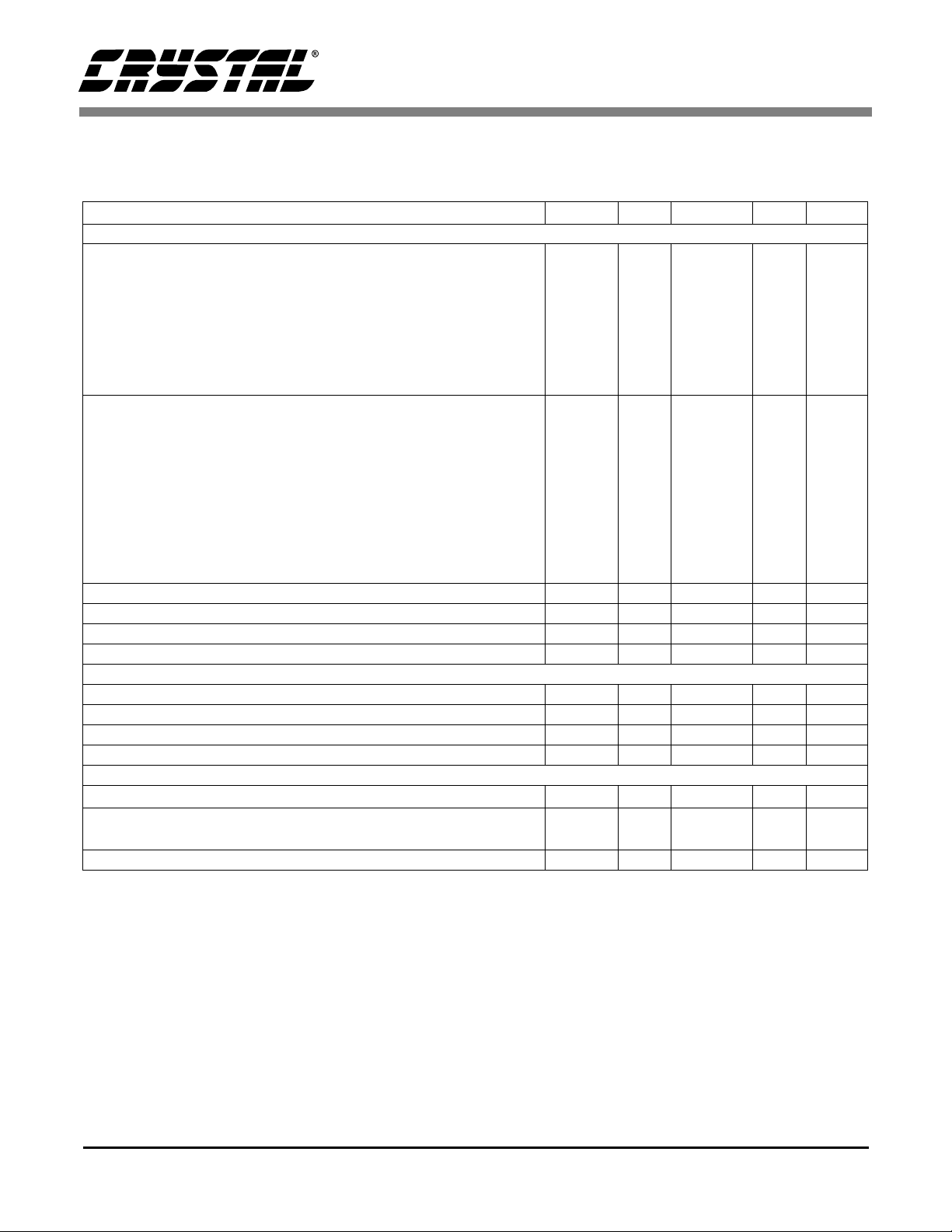
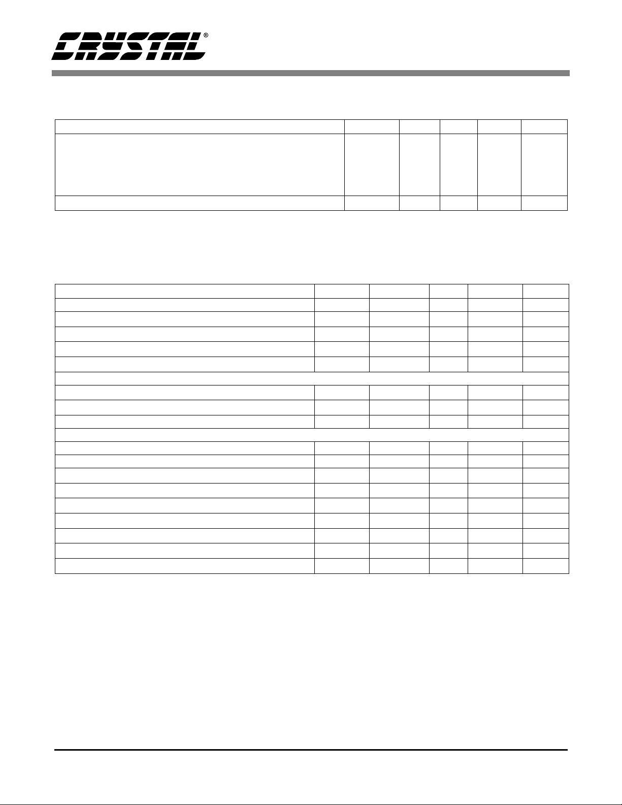
ANALOG CHARACTERISTICS (T
Analog connections as shown in Figure 1; Measurement Bandwidth is 20 Hz to 20 kHz unless otherwise specified;
Logic 0 = 0V, Logic 1 = VD;
Parameter Symbol Min Typ Max Units
Dynamic Performance
Dynamic Range MCLK equal to 24.576 MHz
Fs = 48 kHz in 128x Oversampling Mode (A-weighted)
Fs = 48 kHz in 128x mode
Fs = 96 kHz in 64x mode (A-weighted)
Fs = 96 kHz in 64x mode (40 kHz Bandwidth)
MCLK equal to 12.288 MHz
Fs = 48 kHz in 64x mode (A-weighted)
Fs = 48 kHz in 64x mode
Total Harmonic Distortion + Noise
Fs = 48 kHz in 128x mode -1 dB (Note 1)
Fs = 96 kHz in 64x mode -1 dB (Note 1)
(40 kHz bandwidth) -20 dB (Note 1)
Fs = 48 kHz in 64x mode -1 dB (Note 1)
Total Harmonic Distortion -1 dB (Note 1) THD TBD 0.00056 - %
Interchannel Phase Deviation - 0.0001 - deg
Interchannel Isolation - 120 - dB
Dynamic Range Performance Drift (following calibration) - 0.05 - dB/°C
= 25°C; VA, VL,VD = 5V; Full-scale Input Sinewave, 997 Hz;
A
TBD
-20 dB (Note 1)
-60 dB (Note 1)
-60 dB (Note 1)
-20 dB (Note 1)
-60 dB (Note 1)
TBD
TBD
TBD
TBD
TBD
THD+N
TBD
TBD
TBD
TBD
TBD
TBD
TBD
TBD
TBD
120
117
120
114
117
114
105
97
57
105
97
57
105
97
57
-
-
-
-
-
-
-
-
-
-
-
-
-
-
-
dB
dB
dB
dB
dB
dB
dB
dB
dB
dB
dB
dB
dB
dB
dB
dc Accuracy
Interchannel Gain Mismatch - 0.05 - dB
Gain Error Gain Drift Offset Error (With high pass filter enabled) - 0 - LSB
±
5TBD%
±
100 - ppm/°C
Analog Input
Full-scale Differential Input Voltage (Note 2)
Input Impedance Differential
Common-mode
Common-Mode Rejection Ratio CMRR - 82 - dB
V
IN
Z
IN
TBD 4 TBD V
-
-
4.5
TBD
-
-
pp
Ω
k
Ω
k
Notes: 1. Referenced to typical full-scale differential input voltage (4.0 Vpp).
2. Specified for a fully differential input ±{(AINR+)-(AINR-)}.The ADC accepts input voltages up to the
analog supplies (VA and AGND). Full-scale outputs will be produced for differential inputs beyond
VIN.
* Refer to Parameter Definitions at the end of this data sheet.
Specifications are subject to change without notice.
4 DS229PP2
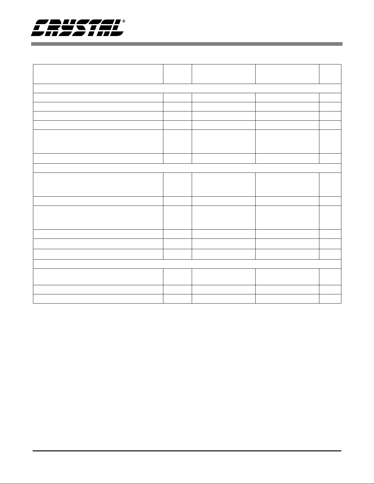
CS5396 CS5397
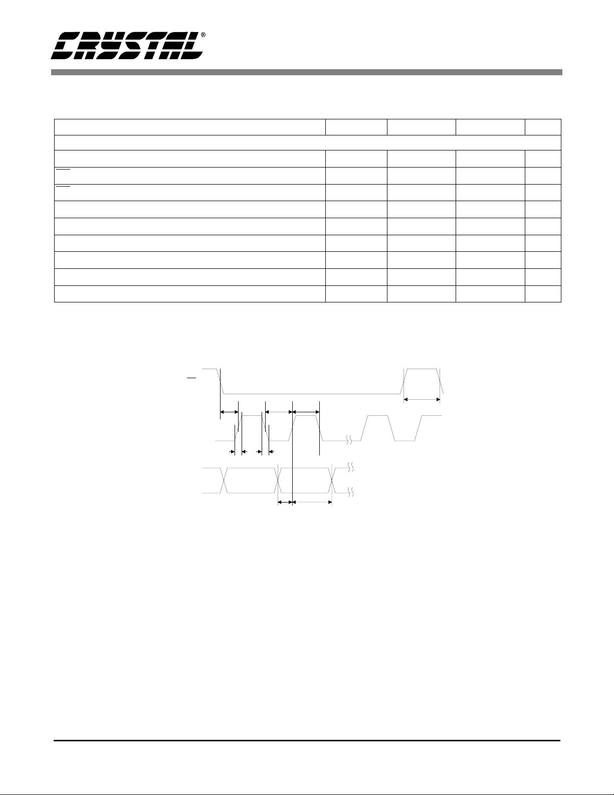
DIGITAL FILTER CHARACTERISTICS (T
Parameter
Symbol Min Typ Max Min Typ Max Unit
= 25 °C; VA, VL,VD = 5V±5%; Fs = 48 kHz)
A
CS5396 CS5397
High-Performance Filter
Passband(-0.01 dB) 0 - 0.4604 0 - 0.3958 Fs
Passband Ripple - Stopband 0.5542 - 63.45 0.4979 - 63.50 Fs
Stopband Attenuation 117 - - 117 - - dB
Group Delay (Fs = Output Sampl e Rate)
128x Oversampling Mode
64x Oversampling Mode
Group Delay Variation vs. Frequency
t
gd
∆
t
gd
-
34/Fs
-
34/Fs
--0.0--0.0
±
0.005 - -
-
-
-
-
34/Fs
34/Fs
±
0.005 dB
-
-
µ
µ
µ
Low Group Delay Filter
Passband(-0.01 dB)
128x Oversampling Mode
64x Oversampling Mode
Passband Ripple - - 0.015 - - 0.015 dB
Stopband
128x Oversampling Mode
64x Oversampling Mode
Stopband Attenuation 86 - 86 - dB
Group Delay (Fs = Output Sampl e Rate)
Group Delay Variation vs. Frequency
t
gd
∆
t
gd
0
0
0.646
0.323
- 10/Fs - - 10/Fs -
--0.0--0.0
-
0.375
-
0.18800
--127.35
63.68
0.646
0.323
-
0.375
-
0.188FsFs
--127.35
63.68FsFs
µ
µ
High Pass Filter Characteristics
Frequency Response-3.0 dB (Note 3)
-0.036 dB (Note 3)
Phase Deviation@ 20Hz (Note 3) - 5.3 - - 5.3 - Deg
Passband Ripple - - 0 - - 0 dB
-1.820-
-1.820-
-
-
Hz
Hz
s
s
s
s
s
Notes: 3. Response shown is for Fs equal to 48 kHz. Filter characteristics scale with Fs.
DS229PP2 5
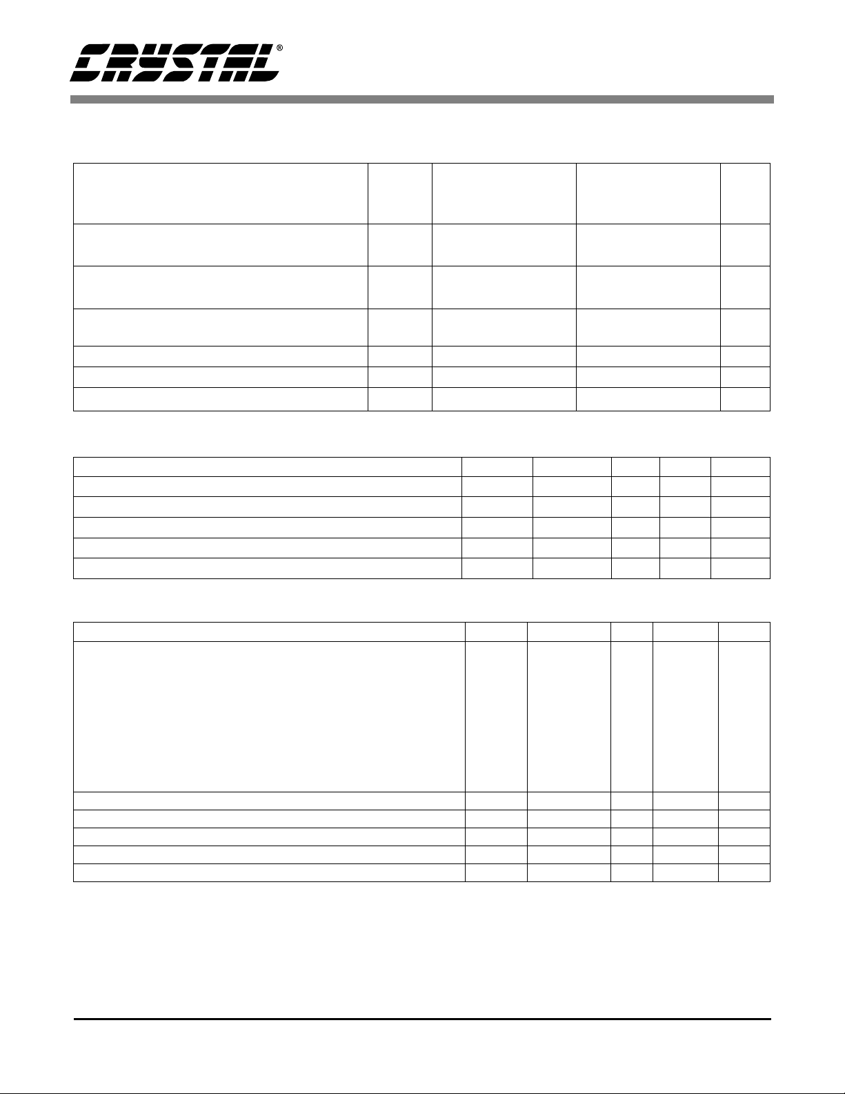
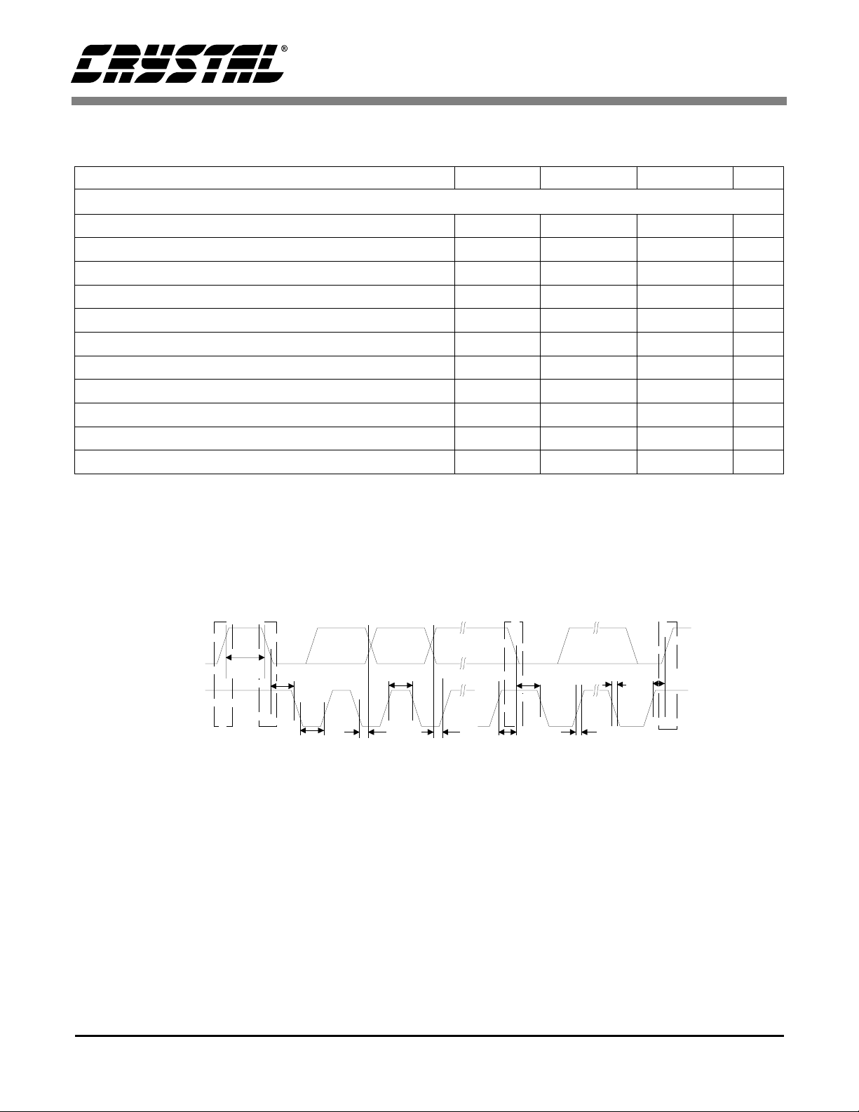
POWER AND THERMAL CHARACTERISTICS
(TA = 25 °C; VA, VL,VD = 5V±5%; Fs = 48 kHz; Master Mode)
CS5396 CS5397
Parameter
Power Supply Current VA+VL
(Normal Operation) VD
Power Supply Current VA+VL
(Power-Down Mode) VD
Power Consumption(Normal Op erati on)
(Power-Down Mode)
64X oversampling
MCLK=12.288 MHz
Symbol Min Typ Max Min Typ Max Unit
-
-
-
-
-
15065TBD
TBD
2
2
107520TBD
I
A
I
D
I
A
I
D
-
128X oversampling
MCLK=24.576 MHz
-
-
-
-
-
-
-
-
-
160
125
3.5
3
TBD
TBDmAmA
-
mA
-
mA
142533TBD-mW
mW
Power Supply Rejection Ratio (1 kHz) PSRR - 65 - - 65 - dB
Allowable Junction Temperature - - 135 - - 135
Junction to Ambient Thermal Impedance
DIGITAL CHARACTERISTICS (T
T
JA
= 25 °C; VA, VL,VD = 5V±5%)
A
-45- -45-
°
C/W
Parameter Symbol Min Typ Max Units
High-Level Input Voltage
Low-Level Input Voltage
High-Level Output Voltage at I
Low-Level Output Voltage at I
Input Leakage Current
V
IH
V
IL
= -20 µAV
o
= 20 µAV
o
OH
OL
I
in
2.4 - - V
--0.8V
VD - 1.0 - - V
--0.4V
--
±10µ
°
C
A
ABSOLUTE MAXIMUM RATINGS (AGND, DGND = 0V, All voltages with respect to ground.)
Parameter Symbol Min Typ Max Units
DC Power Supplies: Analog
Logic
Digital
|VA - VD|
(Note 6)
|VA - VL|
(Note 6)
|VD - VL|
(Note 6)
Input Current (Note 4) I
Analog Input Voltage (Note 5) V
Digital Input Voltage (Note 5) V
Ambient Operating Temperature (Power Applied) T
Storage Temperature T
Notes: 4. Any pin except supplies. Transient currents of up to ±100 mA on the analog input pins will not cause SCR
latch-up.
5. The maximum over/under voltage is limited by the input current.
6. Applies to normal operation. Greater differences during power up/down will not cause SCR latch-up.
WARNING: Operation beyond these limits may result in permanent damage to the device.
Normal operation is not guaranteed at these extremes.
VA
VL
VD
IND
stg
-0.3
-0.3
-0.3
-
-
-
in
IN
--
AGND-0.7 - VA+0.7 V
-
-
-
-
-
-
+6.0
+6.0
+6.0
0.4
0.4
0.4
±
10 mA
V
V
V
V
V
V
-0.3 - VD+0.7 V
A
-55 - +50 °C
-65 - +150 °C
6 DS229PP2
CS5396 CS5397
RECOMMENDED OPERATING CONDITIONS (AGND, DGND = 0V, all voltages with respect
to ground.)
Parameter Symbol Min Typ Max Unit s
DC Power Supplies: Positive Digital
Positive Logic
Positive Analog
|VA - VD|
(Note 6)
Ambient Operating Temperature (Power Applied)
Specifications are subject to change without notice.
VD
VL
VA
T
4.75
4.75
4.75
-
A
-10 - +50
5.0
5.0
5.0
-
5.25
5.25
5.25
0.4
V
V
V
V
°
C
SWITCHING CHARACTERISTICS (T
Logic 1 = VA = VD; C
= 20 pF)
L
= 25 °C; VA = 5V±5%; Inputs: Logic 0 = 0V,
A
Parameter Symbol Min Typ Max Units
Output Sample Rate Fs 2 - 100 kHz
MCLK Period
MCLK Low
MCLK High
MCLK Fall Time
t
clkw
t
t
clkh
t
clkft
clkl
39.06 - 1950 ns
26 - - ns
26 - - ns
--8ns
Master Mode
SCLK falling to LRCK
SCLK falling to SDATA valid
t
mslr
t
sdo
-20 - +20 ns
- - 20 ns
SCLK duty cycle - 50 - %
Slave Mode
LRCK Period 1/Fs 10 - 500
µ
LRCK duty cycle - 50 - %
SCLK Period
SCLK Pulse Width Low
SCLK Pulse Width High
SCLK falling to SDATA valid
LRCK edge to MSB valid
SCLK rising to LRCK edge delay
LRCK edge to rising SCLK setup time
t
sclkw
t
sclkl
t
clkh
t
dss
t
lrdss
t
slr1
t
slr2
4 x t
2 x t
clw
clw
--ns
--ns
60 - - ns
--t
--t
t
+ 20 ns - - ns
clw
t
+ 20 ns - - ns
clw
+ 20 ns ns
clw
+ 20 ns ns
clw
s
DS229PP2 7

CS5396 CS5397
SCLK output
t
mslr
SDATA
t
sdo
LRCK output
MSB MSB-1
SCLK to SDATA & LRCK - MASTER mode
Serial Data Format, Left Justified
SCLK output
t
mslr
SDATA
t
sdo
LRCK output
MSB
SCLK to SDATA & LRCK - MASTER mode
Serial Data Format, I
2
S compatible
SCLK input
LRCK input
SDATA
t
slr1tslr2
t
sclkh
t
lrdss
MSB MSB-1 MSB-2
SCLK to LRCK & SDATA - SLAVE mode
Serial Data Format, Left Justified
SCLK input
LRCK input
t
slr1tslr2
t
sclkh
t
sclkl
t
sclkl
t
dss
t
sclkw
t
sclkw
t
dss
8 DS229PP2
SDATA
SCLK to LRCK & SDATA - SLAVE mode
Serial Data Format, I
2
S compatible
MSB MSB-1
CS5396 CS5397
SPI CONTROL PORT SWITCHING CHARACTERISTICS (T
Inputs: Logic 0 = DGND, Logic 1 = VD; C
Parameter Symbol Min Max Unit
SPI Mode
CCLK Clock Frequency
High Time Between Transmissions
CS
CS
Falling to CCLK Edge
CCLK Low Time
CCLK High Time
CDIN to CCLK Rising Setup Time
CCLK Rising to DATA Hold Time (Note 7)
Rise Time of CCLK and CDIN (Note 8)
Fall Time of CCLK and CDIN (Note 8)
Notes: 7. Data must be held for sufficient time to bridge the transition time of CCLK.
8. For F
< 1 MHz.
SCK
= 20 pF)
L
f
t
t
t
t
t
t
sck
csh
css
scl
sch
dsu
dh
t
r2
t
f2
-6MHz
1.0 - µs
20 - ns
66 - ns
66 - ns
40 - ns
15 - ns
-100ns
-100ns
= 25 °C; VD, VA = 5V ±5%;
A
CS
CCLK
CDIN
t
css
tr2t
t
t
scl
t
f2
dsu
sch
t
dh
t
csh
DS229PP2 9
CS5396 CS5397
I2C CONTROL PORT SWITCHING CHARACTERISTICS (T
Inputs: Logic 0 = DGND, Logic 1 = VD; C
Parameter Symbol Min Max Unit
I2C® Mode (Note 9)
CCLK Clock Frequency
Bus Free Time Between Transmissions
Start Condition Hold Time (prior to first clock pulse)
Clock Low Time
Clock High Time
Setup Time for Repeated Start Condition
CDIN Hold Time from CCLK Falling (Note 10)
CDIN Setup Time to CCLK Rising
Rise Time of Both CDIN and CCLK Lines
Fall Time of Both CDIN and CCLK Lines
Setup Time for Stop Condition
Notes: 9. Use of the I
2C®
bus interface requires a license from Philips.
10. Data must be held for sufficient time to bridge the 300 ns transition time of SCL.
= 20 pF)
L
f
scl
t
buf
t
hdst
t
low
t
high
t
sust
t
hdd
t
sud
t
susp
-100kHz
4.7 - µs
4.0 - µs
4.7 - µs
4.0 - µs
4.7 - µs
0-µs
250 - ns
t
r
t
f
-1µs
-300ns
4.7 - µs
= 25 °C; VD, VA = 5V ±5%;
A
CDIN
CCLK
Stop Start
t
buf
t
t
hdst
low
t
hdd
t
high
t
sud
Repeated
Start
t
sust
t
hdst
Stop
t
f
t
r
t
susp
10 DS229PP2
CS5396 CS5397
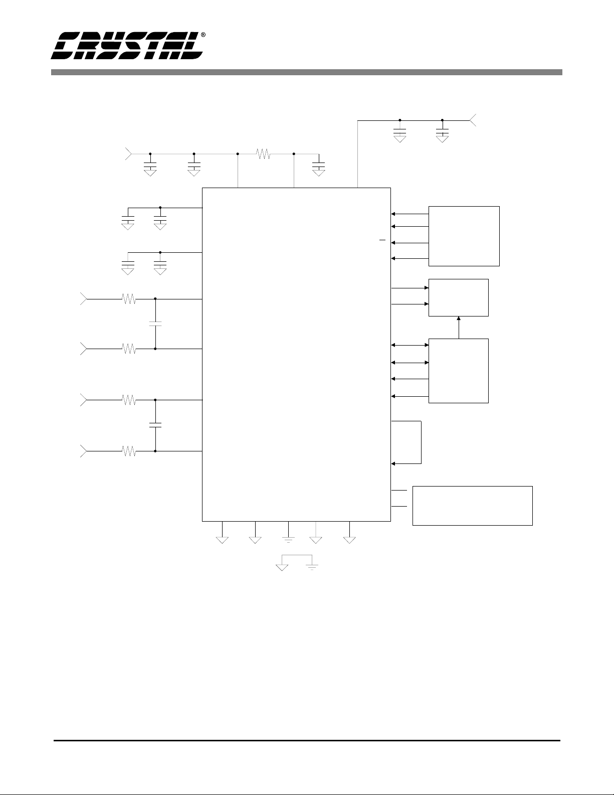
+5V Analog
+
470 µF
100 µF
Left Analog Input +
Left Analog Input -
Right Analog Input +
Right Analog Input -
+
+
39
6.8nF
39
39
6.8nF
39
Ω
Ω
Ω
Ω
1
µ
F
0.1 µF
0.1 µF
1
2
4
5
27
26
0.1 µF
VREF
VCOM
AINL+
AINL-
AINR+
AINR-
5
Ω
VA VL
CS5396/7
A/D CONVERTER
0.1 µF
0.1 µF
2324
11
VD
CS/PDN
CDIN/DFS
CCLK/SM
CAL
SDATA1
SDATA2
LRCK
SCLK
MCLKA
MCLKD
DACTL
ADCTL
19
18
17
10
16
15
13
14
7
20
9
6
+
µ
-Controller/
Configuration
Audio
Data
Processor
Timing
& Clock
+5V Digital
1 µF
Logic
8
TSTO pins should be left
21
floating, with no trace
attached
AGND0
3
22
AGND1LGND DGND AGND2
12 28
TSTO1
TSTO2
25
Figure 1. Typical Connection Diagram
DS229PP2 11
CS5396 CS5397
GENERAL DESCRIPTION
The CS5396/97 is a 24-bit, stereo A/D converter
designed for stereo digital audio applications. The
analog input channels are simultaneously sampled
by separate, patented, 7th-order tri-level delta-sigma modulators at either 128 or 64 times the output
sample rate (64× Fs or 128× Fs) of the device. The
resulting serial bit streams are digitally filtered,
yielding pairs of 24-bit values at output sample
rates (Fs) of up to 100 kHz . This technique yields
nearly ideal conversion performance independent
of input frequency and amplitude. The converter
does not require difficult-to-design or expensive
anti-alias filters, and it does not require external
sample-and-hold amplifiers or voltage references.
Only normal power supply decoupling components, voltage reference bypass capacitors and a
single resistor and capacitor on each input for antialiasing are required, as shown in Figure 1. An onchip voltage reference provides for a differential
input signal range of 4.0 Vpp. The device also contains a high pass filter, implemented digitally after
the decimation filter, to completely eliminate any
internal offsets in the converter or any offsets
present at the input circuitry to the device. Output
data is available in serial form, coded as 2’s complement 24-bit numbers. For more information on
delta-sigma modulation techniques see the references at the end of this data sheet.
Stand-Alone vs. Control Port Mode
The CS5396/97 can operate in either Stand-Alone
or Control Port Mode. The functionality of pins 17,
18 and 19 is established upon entering either the
Stand-Alone or Control Port mode, as described in
the Pin Description section.
• 128× Oversampling Mode
• Reduction of 24-bit data to 20, 18 or 16-bit data
with psychoacoustically optimized dither
• Programmability of psychoacoustic filter coefficients
• Peak Input Signal Level Monitor with either
High Resolution or Bar Graph mode selection
• Signal inversion
• High pass filter defeat
• Mute
• Access to the digital filter to allow the input of
external digital audio data to produce a two-toone decimated output and/or psychoacoustic bit
reduction.
STAND-ALONE MODE
Master Clock - Stand-Alone Mode
The master clock is the clock source for the deltasigma modulator sampling (MCLKA) and digital
filters (MCLKD). The required MCLKA/D frequency is determined by the desired Fs an d must be
256× Fs. Table 1 shows some common master
clock frequencies.
LRCK
(kHz)
32 8.192 2.048
44.1 1 1.2896 2.822
48 12.288 3.072
64 16.384 4.096
88.2 22.5792 5.6448
96 24.576 6.144
Table 1. Common Clock Frequencies for Stand-Alone
MCLKA/D
(MHz)
Mode
SCLK
(MHz)
The Control Port Mode requires a micro-controller
and allows access to many additional features,
which include:
Serial Data Interface - Stand-Alone Mode
The CS5396/97 supports two serial data formats
which are selected via the digital format select pin,
DFS. The digital output format determines the relationship between the serial data, left/right clock and
serial clock. Figures 2 and 3 detail the interface for-
12 DS229PP2

CS5396 CS5397
mats. The serial data interface is accomplished via
the serial data outputs; SDATA1 and SDATA2; serial data clock, SCLK, and the left/right clock,
LRCK. The serial nature of the output data results
in the left and right data words being read at different times. However, the samples within an LRCK
cycle represent simultaneously sampled analog inputs.
Serial Data- Stand-Alone Mode
The serial data block consists of 24 bits of audio
data presented in 2’s-complement format with the
MSB-first. The data is clocked from SDATA1 and
SDATA2 by the serial clock and the channel is determined by the Left/Right clock. The full pre cision
24-bit data is available on SDATA1 and the output
from the low group delay filter is available on
SDATA2.
Serial Clock - Stand-Alone Mode
The serial clock shifts the digitized audio data from
the internal data registers via the SDATA1 and
SDATA2 pins. SCLK is an output in Master Mode
where internal dividers will divide the master clock
by 4 to generate a serial clock which is 64× Fs. In
Slave Mode, SCLK is an input with a serial clock
typically between 48× and 128× Fs. However, it is
recommended that SCLK be equal to 64×, though
other frequencies are possible, to avoid potential
interference effects which may degrade system performance.
Left/Right Clock - Stand-Alone Mode
The Left/Right clock, LRCK, determines which
channel, left or right, is to be output on SDATA1
and SDATA2. In Master Mode, LRCK is an output
whose frequency is equal to Fs. In Slave Mode,
LRCK is an input whose frequency must be equal
to Fs and synchronous to MCLKA/D.
Master Mode - Stand-Alone Mode
In Master mode, SCLK and LRCK are outputs
which are internally derived from the master clock.
Internal dividers will divide MCLKA/D by 4 to
generate a SCLK which is 64× Fs and by 256 to
generate a LRCK which is equal to Fs. The
CS5396/97 is placed in the Master mode with the
slave/master pin, S/M, low.
Slave Mode - Stand-Alone Mode
LRCK and SCLK become inputs in SLAVE mode.
LRCK must be externally derived from MCLKA/D
and be equal to Fs. It is recommended that SCLK
be equal to 64×. Other frequencies between 48×
and 128× Fs are possible but may degrade system
performance due to interfere nce effects. The ma ster clock frequency must be 256× Fs. The
CS5396/97 is placed in the Slave mode with the
slave/master pin, S/M, high.
High Pass Filter - Stand-Alone Mode
The CS5396/97 includes a high pass filter after the
decimator to remove the DC offsets introduced by
the analog buffer stage and the CS5396/97 analog
modulator. The characteristics of this first-order
high pass filter are outlined below, for Fs equal to
48 kHz. This filter response scales linearly with
sample rate.
Frequency response: -3 dB @ 1.8 Hz
-0.036 dB @ 20 Hz
Phase deviation: 5.3 degrees @ 20 Hz
Passband ripple: None
Power-up and Calibration - Stand-Alone Mode
The delta-sigma modulators settle in a matter of
microseconds after the analog section is powered,
either through the application of power or by exiting the power-down mode. However, the voltage
reference will take a much longer time to reach a final value due to the presence of external capacitance on the VREF pin. A time delay of
approximately 10ms/µF is required after applying
power to the device or after exiting a power down
state.
DS229PP2 13

CS5396 CS5397
A calibration of the tri-level delta-sigma modulator
should always be initiated following power-up and
after allowing sufficient time for the voltage on th e
external VREF capacitor to settle. This is required
to minimize noise and distortion. It is also advised
that the CS5396/97 be calibrated after the device
has reached thermal equilibrium, approximately 10
seconds, to maximize performance.
Synchronization of Multiple Devices Stand Alone Mode
In systems where multiple ADCs are required, care
must be taken to achieve simultaneous sampling. It
is recommended that the rising edge of the CAL
signal be timed with a falling edge of MCLK to ensure that all devices will initiate a calibration and
synchronization sequence on the same rising edge
of MCLK. The absence of re-timing of the CAL
signal can result in a sampling difference of one
MCLK period.
CONTROL PORT MODE
Access to Control Port Mode
The mode selection between Stand-Alone and Control Port Mode is determined by the state of the
SDATA1 pin 250 MCLK cycles following the internal power-on reset. A 47 kΩ pull-up resistor on
SDATA1 will select the Control Port Mode. However, the control port will not respond to CCLK and
CDIN until the pull-up on the SDATA1 pin is released.
Internal Power-On Reset
The timing required to determine Control port
mode and I2S/SPI mode is based on an internal
power-on reset. The internal power-on reset requires the power supply to exceed a threshold voltage. However, there is no external indication of
when the internal reset is activated. If precise timing of the Control port and I2S/SPI decisions is required, MCLK should not be applied until the
power supply has stabilized.
LRCK
SCLK
SDATA 23 22 7 6 23 22
9 7654321089
Left
5432108
MASTER
24-Bit Left Justified Data
Data Valid on Rising Edge of 64x SCLK
MCLK equal to 256x Fs
Right
23 22
SLAVE
24-Bit Left Justified Data
Data Valid on Rising Edge of SCLK
MCLK equal to 256x Fs
Figure 2. Serial Data Format 0, Stand-Alone Mode, DFS low. Left Justified.
LRCK
SCLK
SDATA 23 22 8 7 23 22
Left Right
6543210 8765432109 9
MASTER
2
I S 24-Bit Data
Data Valid on Rising Edge of 64x SCLK
MCLK equal to 256x Fs
23 22
SLAVE
2
I S 24-Bit Data
Data Valid on Rising Edge of SCLK
MCLK equal to 256x Fs
Figure 3. Serial Data Format 1, Stand-Alone Mode, DFS High. I2S compatible
14 DS229PP2

CS5396 CS5397
Master Clock - Control Port Mode
The master clock is the clock source for the deltasigma modulator sampling (MCLKA) and digital
filters (MCLKD). The required MCLKA/D frequency is determined by the desired Fs and the chosen Oversampling Mode. Table 2 shows some
common master clock frequencies.
64× vs. 128× Oversampling Modes
The CS5396/97 can operate in a 64× Oversampling
Mode with a 256× master clock (MCLKA/D) at a
maximum sample rate of 100 kHz. The device can
also operate in a 128× Oversampling Mode with a
512× master clock (MCLKA/D) where the maximum Fs is 50 kHz. Notice that the required master
clock is 24.576 MHz for Fs equal to either 48 kHz
in the 128× Oversampling Mode or 96 kHz in the
64× Oversampling Mode. The sampling mode is
set via the control register which alters the de cimation ratio of the digital filter. The 64× Oversampling Mode is the default mode. Table 2 shows
some common clock frequencies for both modes.
Refer to Appendix A for additional discussion of
64× vs. 128× Oversampling Modes.
LRCK
(kHz)
32 64 8.192 2.048
44.1 64 11.2 896 2.822
48 64 12.2 88 3.072
32 12 8 16.384 4.096
44.1 128 22.5792 5.6448
48 12 8 24.576 6.144
64 64 16.3 84 4.096
88.2 64 22.5792 5.6448
96 64 24.5 76 6.144
Table 2. Common Clock Frequencies
Over-
sampling
MCLKA/D
(MHz)
SCLK
(MHz)
Serial Data Interface - Control Port Mode
The CS5396/97 supports two serial data formats
which are selected via the control register. The digital output format determines the relationship between the serial data, left/right clock and serial
clock. Figures 4 - 7 detail the interface formats.
The serial data interface is accomplished via the serial data outputs; SDATA1 and SDATA2, serial
data clock, SCLK, and the left/right clock, LRCK.
The serial nature of the output data results in the left
and right data words being read at different times.
However, the samples within an LRCK cycle represent simultaneously sampled analog inputs.
Serial Data - Control Port Mode
The serial data block is presented in 2’s-complement format with the MSB-first. The data is clocked
from SDATA1 and SDATA2 by the serial clock
and the channel is determined by the Left/Right
clock. The full precision 24 bit data is available on
SDATA1 and the output from the low group delay
is available on SDATA2.
The serial data can be followed by 8 Peak Signal
Level, PSL, bits as shown in Figures 4 - 7 if the
PKEN bit is set. Refer to the Dual Audio Output
section of this data sheet for further discussion of
SDATA1 and SDATA2 options.
Serial Clock - Control Port Mode
The serial clock shifts the digitized audio data from
the internal data registers via SDATA1 and
SDATA2. SCLK is an output in Master Mode
where internal dividers will divide the master cloc k
by 4 to generate a serial clock which is 64×Fs in
the 64× Oversampling Mode. In the 128× Oversampling Mode, internal dividers will divide
MCLKA/D by 4 to generate a SCLK which is 128×
Fs. In Slave Mode, SCLK is an input with a serial
clock typically between 48× and 128× Fs. It is recommended that SCLK be equal to 64× in the 64×
Oversampling Mode and equal to 128× in the 128×
Oversampling Mode to avoid possible system performance degradation due to interference effects.
Left/Right Clock -Control Port Mode
The Left/Right clock, LRCK, determines which
channel, left or right, is to be output on SDATA1
DS229PP2 15

CS5396 CS5397
LRCK
SCLK
SDATA P1 P024 23 9 P7 P6 P5 P4 P3 P28 24 23
Left Right
10325476 76543210
MASTER
24-Bit Left Justified Data
Data Valid on Rising Edge of 64x SCLK
MCLK equal to 256x Fs
SLAVE
24-Bit Lef t Justifi ed Data
Data Valid on Rising Edge of SCLK
MCLK equal to 256x Fs
P1 P024 23 9 P7 P6 P5 P4 P3 P28
Figure 4. Control Port Mode, Serial Data. Left Justified. 64x Oversampling Mode
The peak signal level bits are available only if Bit 6 of Byte 7 is set.
LRCK
SCLK
SDATA P1 P024 23 9 P7 P6 P5 P4 P3 P28 24 23P1 P024 23 9 P7 P6 P5 P4 P3 P2810325476 76543210
Left Right
MASTER
2
I S 24-Bit Data
Data Valid on Rising Edge of 64x SCLK
MCLK equal to 256x Fs
SLAVE
2
I S 24-Bit Data
Data Vali d on Rising Edge of S CL K
MCLK equal to 256x Fs
Figure 5. Control Port Mode, Serial Data. I2S Compatible. 64x Oversampling Mode.
The peak signal level bits are available only if Bit 6 of Byte 7 is set.
LRCK
SCLK
SDATA P1 P023 22 P7 P6 P5 P4 P3 P2
10 P1 P0P7 P6 P5 P4 P3 P2 23 2210
Left Right
MASTER
24-Bit Left Justified Data
Data Valid on Rising Edge of 128x SCLK
MCLK equal to 512x Fs
Figure 6. Control Port Mode, Serial Data. Left Justified. 128x Oversampling Mode
The peak signal level bits are available only if Bit 6 of Byte 7 is set.
LRCK
SCLK
SDATA P1 P023 22 P7 P6 P5 P4 P3 P2
Left Right
MASTER
2
I S 24-Bit Data
Data Valid on Rising Edge of 128x SCLK
MCLK equal to 512x Fs
Figure 7. Control Port Mode, Serial Data. I2S Compatible. 128x Oversampling Mode.
The peak signal level bits are available only if Bit 6 of Byte 7 is set.
23 22
SLAVE
24-Bit Left Justified Data
Data Valid on Rising Edge of SCLK
MCLK equal to 512x Fs
23 2210 P1 P0P7 P6 P5 P4 P3 P2 23 2210
SLAVE
2
I S 24-Bit Data
Data Valid on Rising Edge of SCLK
MCLK equal to 512x Fs
16 DS229PP2

CS5396 CS5397
and SDATA2. In Master Mode, LRCK is an output
whose frequency is equal to Fs. In Slave Mode,
LRCK is an input whose frequency must be equal
to Fs and synchronous to MCLKA/D.
Master Mode- Control Port Mode
In Master mode, SCLK and LRCK are outputs
which are internally derived from the master clock.
In the 64× Oversampling Mode, internal dividers
will divide MCLKA/D by 4 to generate a SCLK
which is 64× Fs and by 256 to generate a LRCK
which is equal to Fs. In the 128× Oversampling
Mode, internal dividers will divide MCLKA/D by
4 to generate a SCLK which is 128× Fs and by 512
to generate a LRCK which is equal to Fs. The
CS5396/97 is placed in the Master mode via the
control register.
Slave Mode - Control Port Mode
LRCK and SCLK become inputs in SLAVE mode.
LRCK must be externally derived from MCLKA/D
and be equal to Fs. It is recommended that SCLK
be equal to 64× in the 64× Oversampling Mode and
equal to 128× in the 128× Oversampling Mode.
Other frequencies are possible but may degrade
system performance due to interference effects.
The CS5396/97 is placed in the Slave mode via the
control register.
Synchronization of Multiple Devices Control Port Mode
devices to have individual addresses, synchronization can be accomplished by;
1) Disable the address enable bit (ADDREN) in
register 7
2) Issue a system broadcast FSTART command
synchronized with CCLK.
3) Reset the ADDREN bit.
Power-up and Calibration - Control Port Mode
The delta-sigma modulators settle in a matter of
microseconds after the analog section is powered,
either through the application of power or by exiting the power-down mode. However, the voltage
reference will take a much longer time to reach a final value due to the presence of external capacitance on the VREF pin. A time delay of
approximately 10ms/µF is required after applying
power to the device or after exiting a power down
state.
A calibration of the tri-level delta-sigma modulator
should always be initiated following power-up and
after allowing sufficient time for the voltage on the
external VREF capacitor to settle. This is required
to minimize noise and distortion. It is also advised
that the CS5396/97 be calibrated after the device
has reached thermal equilibrium to maximize performance. A calibration sequence requires the following commands;
In systems where multiple ADCs are required, care
must be taken to achieve simultaneous sampling.
The FSTART bit in register 1 controls the synchronization of the internal clocks and sampling process between the analog modulator and the digital
filter. Multiple ADCs can be synchronized if the
FSTART command is initiated on the same edge of
MCLK. This can be accomplished by re-timing the
CCLK clock with the falling edge of MCLK. This
is a relatively simple matter if the ADCs have the
same address. However, if the system requires the
DS229PP2 17
1) set the FSTART bit
2) set the GND CAL bit
3) set the CAL bit
4) Wait a minimum of 2050 LRCK periods in the
128x mode or 4100 LRCK periods in the 64x
mode.
5) Remove GND CAL
High Pass Filter -Control Port Mode
The CS5396/97 includes a high pass filter after the
decimator to remove the DC offsets introduced by

CS5396 CS5397
the analog buffer stage and the CS5396/97 analog
modulator. The high pass filter can be defeated
with the control register. It is also possible to write
to the left/right offset registers to establish a predetermined offset.
The characteristics of this first-order high pass filter are outlined below for Fs equal to 48 kHz. The
filter response scales linearly with sample rate.
Frequency response: -3 dB @ 1.8 Hz
-0.036 dB @ 20 Hz
Phase deviation: 5.3 degrees @ 20 Hz
Passband ripple: None
Input Level Monitoring - Control Port Mode
The CS5396/97 includes independent Peak Input
Level Monitoring for each channel. The analog-todigital converter continually monitors the peak digital signal for both channels and records these values in the Active registers. This information can be
transferred to the Output registers by writing the
PU (Peak Update) bit which will also reset the Active register. The Active register contains the peak
signal level since the previous peak update request.
The 8-bit contents of the output registers are available in both interface modes. The peak signal level
information is available in two formats - High Resolution Mode and Bar Graph Mode. The output format is controlled via the control register.
High Resolution Mode
P7 - Overrange
0 - Analog input less than full-scale level
1 - Analog input greater than full-scale
P6 - Idle channel
0 - Analog input >-60 dB from full-scale
1 - Analog input <-60 dB from full-scale
P5 to P0 - Input Level Bits (1 dB steps)
Inputs <0 dB P5 - P0
0 dB 000000
-1 dB 000001
-2 dB 000010
-60 dB 111100
Bar Graph Mode
This mode provides a decoded output format which
indicates the peak input signal level in a “Bar
Graph” format which can be used to drive front
panel LEDs. This decoded output can be used to
drive front panel LEDs.
Input Level T7 - T0
Overflow 11111111
0 dB to -3 dB 01111111
-3 dB to -6 dB 00111111
-6 dB to -10 dB 00011111
-10 dB to -20 dB 00001111
-20 dB to -30 dB 00000111
-30 dB to -40 dB 00000011
-40 dB to -60 dB 00000001
< - 60 dB 00000000
Bits P7-P0 indicate the Peak Signal Level (PSL)
since the previous peak update (or previous write of
the PU bit). If the ADC input level is less than fullscale, bits P5-P0 represent the peak value from 60 dB to 0 dB of full scale in 1 dB steps. The PSL
outputs are accurate to within 0.25 dB. Bit P6 provides a coarse means of determining an ADC input
idle condition. Bit P7 indicates an ADC overflow
condition if the ADC input level is greater than
full-scale.
18 DS229PP2
Dual Digital Audio Outputs
The CS5396/97 contains two stereo digital audio
output channels - SDATA1 and SDATA2. These
audio output channels are completely ind ependent,
as SDATA1 can contain 24-bit audio data simultaneous with p sychoacous tic au dio data o n SDAT A2.
Another example of this independence is 24-bit audio data output on SDATA1 simultan eou sly wit h a
low group delay output on SDATA2.
The audio output formats are completely programmable through the I2C/SPI µC interface. The output

CS5396 CS5397
formats include: inverted output, psychoacoustic
output (16-bit, 18-bit, 20-bit), and low group delay
output.
Psychoacoustic Filter
The CS5396/97 includes a programmable 10 tap
digital filter which can be used to perform psychoacoustic noise-shaping of the audio spectrum if
desired. The filter can implement a variety of 16bit, 18-bit, or 20-bit noise-shaped responses by
setting the digital filter coefficients. Further discussion of the psychoacoustic filter can be found
in Appendix C.
Appendix B discusses an application using the psychoacoustic filter independently of the A/D converter function. In this mode, SDATA2 becomes an
input to the psychoacoustic filter stage and
SDATA1 is the digital audio output.
Low Group Delay Filter
The characteristics of the low group delay filter are
shown in Figures 17 - 24.
that is to be updated. The next 8 bits are the data
which will be placed into the register designated by
the MAP.
The CS5396/97 has a MAP auto increment, which
will increment the MAP after each byte is written,
allowing block writes of successive registers.
I2C Mode
In I2C mode, CDIN is a bidirectional data line.
Data is clocked into and out of the part by CCLK.
The eighth bit of the address byte is the R/W bit
(high for a read, low for a write). If the operation is
a write, the next byte is the Memory Addres s Pointer which selects the register to be read or writt en. If
the operation is a read, the contents of the register
pointed to by the Memory Address Pointer will be
output. MAP allows successive reads or writes of
consecutive registers. Each byte is separated by an
acknowledge bit. Use of the I2C bus compatible interface requires a license from Philips. I2C bus in a
registered trademark of Philips Semiconductors.
µC Interface Formats
The device supports either SPI or I2C interface formats. The CS5396/97 monitors the state of CS during power-up and will configure to an SPI interface
if the pin is held low. Conversely, if the pin is held
high, the port will configure to a I2C interface.
SPI Mode
In SPI mode, CS is the chip select signal, CCLK is
the µC bit clock and CDIN is the input data line
from the microcontroller. Notice that it is not possible to read the CS5396/97 registers in SPI mode
due to the lack of a data output pin.
To write to a register, bring CS low. The first 7 bits
on CDIN are the chip address, and must be zero.
The eighth bit is a read/write indicator (R/W)
which must be low.
The next 8 bits form the Memory Address Pointer
(MAP), which is set to the address of the register
Establishing the Chip Address in I2C Mode
Connecting SDATA1 pin and CS to 5 volts during
power-up will set the device to the Control Port and
I2C mode. However, the control port will not respond to CCLK and CDATA until the hold on the
SDATA1 pin is released. The chip address can be
set by:
1) Release the hold on the SDATA1 pin of the device to be addressed.
2) Program the chip address and set the Address
Enable bit, addren, which will prevent further
communication to this device without the correct address.
3) Repeat steps 1 and 2 for the remaining devices
on the bus.
ANALOG CONNECTIONS - ALL MODES
Figure 1 shows the analog input connections. The
analog inputs are presented differentially to the
DS229PP2 19

CS5396 CS5397
+3.5 V
+2.5 V
+1.5 V
+3.5 V
+2.5 V
+1.5 V
CS5396/97
AIN+
AIN-
Full Scale Input level= (AIN+) - (AIN-)= 4.0 Vpp
Figure 8. Full scale input voltage
modulators via the AINR+/- and AINL+/- pins.
Each analog input will accept a maximum of
2.0 Vpp. The + and - input signals are 180° out of
phase resulting in a differential input voltage of
4.0 Vpp. Figure 8 shows the input signal levels for
full scale.
to the sensitivity of this node, the circuit traces attached to these pins must be minimal in length and
no load current may be taken from VREF. It is possible to use VCOM as a reference voltage to bias
the input buffer circuits, if the circuit trace is very
short and VCOM is buffered at the converter (refer
to the CDB53965/97). The recommended decoupling scheme for VREF, Figure 1, is a 470 µF electrolytic capacitor and a 0.1 µF ceramic capacitor
connected from VREF to AGND. The recommended decoupling scheme for VCOM, Figure 1, is a
100 µF electrolytic capacitor and a 0.1 µF ceramic
capacitor connected from VCOM to AGND.
GROUNDING AND POWER SUPPLY DECOUPLING - ALL MODES
As with any high resolution converter, the ADC requires careful attention to power supply and
The analog modulator samples the input at
6.144 MHz (MCLK=24.576 MHz) corresponding
to Fs equal to 48 kHz in the 128× Oversampling
Mode and Fs equal to 96 kHz in the 64× Oversampling Mode. The digital filter will reject signals
within the stopband of the filter. However, there is
no rejection for input signals which are
(n ×6.144 MHz) ± the digital passband frequency,
where n=0,1,2,...A 39 Ω resistor in series with the
analog input and a 6.8 nF COG capacitor between
the inputs will attenuate any noise energy at
6.144 MHz, in addition to providing the optimum
source impedance for the modulators. The use of
capacitors which have a large voltage coefficient
(such as general purpose ceramics) must be avoided since these can degrade signal linearity. If active
circuitry precedes the ADC, it is recommended that
the above RC filter is placed between the active circuitry and the AINR and AINL pins. The above example frequencies scale linearly with output
sample rate.
The on-chip voltage reference and the common
mode voltage are available at VREF and VCOM
for the purpose of decoupling only. However, due
20 DS229PP2
grounding arrangements if its potential performance is to be realized. Figure 1 shows the recommended power arrangements, with VA and VL
connected to a clean +5 V supply. VD, which powers the digital filter, should be run from the system
+5 V logic supply, provided that it is not excessively noisy (< ±50 mV pk-to-pk). Decoupling capacitors should be as near to the ADC as possible, with
the low value ceramic capacitor being the nearest.
The printed circuit board layout should have separate analog and digital regions and ground planes,
with the ADC straddling the boundary. All signals,
especially clocks, should be kept away from the
VREF pin in order to avoid unwanted coupling into
the modulators. The VREF decoupling capacitors,
particularly the 0.01 µF, must be positioned to minimize the electrical path from VREF and pin 3,
AGND. The CDB5396/97 evaluation board demonstrates the optimum layout and power supply arrangements, as well as allowing fast evaluation of
the ADC.
To minimize digital noise, connect the ADC digital
outputs only to CMOS inputs.

CS5396 CS5397
DIGITAL FILTER PLOTS
Figures 9-24 show the performance of the digital
filters included in the ADC. All plots are normalized to Fs. Assuming a sample rate of 48 kHz, the
Magnitude (dB)
Normalized Frequency (Fs)
Figure 9. CS5396 Stop Band Attenuation Figure 10. CS5396 Passband Ripple
0.5 frequency point on the plot refers to 24 kHz.
The filter frequency response scales precisely with
Fs.
Magnitude (d B)
Normalized Fr equ enc y (F s)
Magnitude (dB)
Normalized Frequency (Fs)
Magnitude (dB)
Normalized Frequency (Fs)
Figure 11. CS5396 Transition Band Figure 12. CS5396 Transition Band
DS229PP2 21

CS5396 CS5397
Magnitude (d B)
Normalized Frequency (Fs)
Magnitude (d B)
Normalized Fr equ enc y (F s)
Figure 13. CS5397 Stop Band Attenuation Figure 14. CS5397 Passband Ripple
Magnitude (dB)
Magnitude (dB)
Normalized Frequency (Fs)
Normalized Frequency (Fs)
Figure 15. CS5397 Transition Band Figure 16. CS5397 Transition Band
22 DS229PP2

CS5396 CS5397
Magnitude (dB)
Normalized Frequency (Fs)
Figure 17. Low Group Delay Filter
Stop Band Attenuation
64x Oversampling Mo de
Magnitude (dB)
Magnitude (d B)
Normalized Fr equ enc y (F s)
Figure 18. Low Group Delay Filter
Passband Ripple
64x Oversampling Mode
Magnitude (dB)
Normalized Frequency (F s)
Figure 19. Low Group Delay Filter
Transition Band
64x Oversampling Mo de
Figure 20. Low Group Delay Filter
64x Oversampling Mode
Normalized Frequency (F s)
Transition Band
DS229PP2 23

CS5396 CS5397
Figure 21. Low Group Delay Filter
Stop Band Attenuation
128x Oversampling Mode
Figure 23. Low Group Delay Filter
Transition Band
128x Oversampling Mode
Figure 22. Low Group Delay Filter
Passband Ripple
128x Oversampling Mode
Figure 24. Low Group Delay Filter
Transition Band
128x Oversampling Mode
24 DS229PP2

CS5396 CS5397
REGISTER DESCRIPTION
** “default” ==> bit status after power-up-sequence
Analog control (address 00000001)
76543210
fstart gndcal aapd adpd 1bit
00000
FSTART (Frame start)Default = ‘0’.
This bit must be set to ‘1’ to synchronize the modulator output and the decimation filter input
and is automatically reset to ‘0’ after a “fstart” pulse is sent to the analog and digital block.
GNDCAL (Ground calibration enable)
Default = ‘0’.
Modulator input is tied to internal “Vcom” when this bit is ‘1’.
AAPD (Analog Section of modulator in power down)
Default = ‘0’.
The analog section of the modulator is in power down mode when aapd = ‘1’.
ADPD (Digital Section of modulato r in power down )
Default = ‘0’.
The digital section on the modulator is in power down mode when adpd = ‘1’.
TEST BIT Default =’0’.
Must remain at 0.
Mode (address 00000010)
76 5 43210
128x/64x
00 0 00000
128x/64x Default = ‘0’.
CAL (System calibration enable)
Change_sign (Change Sign enable)
_LR/LL (Left-Right output disable) Default = ‘0’.
cal change_sign _LR/LL _hpen s/_m DFS mute
Oversampling ratio is 128 when this bit is ‘1’ and 64 when this bit is ‘0’.
Default = ‘0’.
Setting this bit to ‘1’ will initiate calibration.
This bit is automatically reset to ‘0’ following calibration.
Default = ‘0’.
A ‘1’ will interchange the analog input paths within each channel resulting in a phase inversion
of the analog signal. This bit applies to both channels.
If this bit is ‘0’, SDATA1 will output the Left and Right channel data from the sdata1 source and
SDATA2 will output the Left and Right channel data from the sdata2 source as described elsewhere in the data sheet.
If this bit is set to ‘1’, the Left channel data from sdata1 source and sdata2 source (stored in
Audio port register) will be sent out in SDATA1. SDATA2 will output all the Right channel data.
DS229PP2 25

HPEN (HP enable) Default = ‘0’.
The highpass filter will be disabled when _HPEN = ‘1’. The highpass filter will be automatically
enabled following calibration.
S/_M (Slave / Master mode) Default = ‘0’.
In master mode, LRCK, and SCLK are outputs. In slave mode, LRCK and SCLK are inputs.
This bit is ignored when sdata1 is used as input port in “fir2in” or “psychoin” mode (refer to Digital control & Tag register and Appendix B).
CS5396 CS5397
DFS (Digital Format Select)Default = ‘0’.
Output of seri al data complie s with I
2
S standard when DFS is 1. Out-
put of serial data is Left Justified when DFS is 0.
MUTE Default = ‘0’.
Data at SDATA1 and SDATA2 is always ‘0’ when this set to ‘1’.
Audio port (address 00000011)
76543210
24bit
(sdata1)
10000001
24bit(SDATA1) Default = ‘1’.
24bit(SDATA2) Default = ‘0’.
psycho(SDATA1) Default = ‘0’.
24bit
(sdata2)
psycho
(sdata1)
psycho
(sdata2)
psel18/_16 psel20/_16
lgd
(sdata1)
lgd
(sdata2)
A ‘1’ enables the serial audio port 1 to transmit the 24-bit high precision output.
This bit must be set to ‘0’ to enable other SDATA1 output options.
A ‘1’ enables the serial audio port 2 to transmit 24-bit high precision output. This bit must be set
to ‘0’ to enable other SDATA2 output options.
psychoacoustic output will be the data at the serial audio port 1 if this bit is ‘1’ and all other bits
of the port are set to ‘0’.
psycho(SDATA2) Default = ‘0’.
psychoacoustic output will be the data at the serial audio port 2 if this bit is ‘1’ and all other bits
of the port are set to ‘0’.
psel18/_16(Psycho 18bit or 16bit)
Default = ‘0’.
This bit indicates the number of output bit if the psychoacoustic filter is chosen as output. A ‘0’
here allows 16 bits output whereas a ‘1’ allows 18 bits output as long as “psel20/_16” is ‘0’.
psel20/_16(Psycho 20bit)
Default = ‘0’.
This bit has the highest priority when setting the number of output bit of psychoacoustic filter. If
this bit is ‘1’, the output is set to 20-bit regardless of the status of “psel18/_16”.
LGD(sdata1) Default = ‘0’.
24-bit low-group-delay filter output will go through a highpass filter if “_hpen” bit in the Mode
register is ‘0’. The LGD output will be the data at the serial audio port 1 if this bit is ‘1’ and all
other bits of the port set to ‘0’.
LGD(sdata2) Default = ‘1’.
26 DS229PP2

CS5396 CS5397
24-bit low-group-delay filter output will go through a high passfilter if “_hpen” bit in the Mode
register is ‘0’. If “_hpen” is ‘1’, data at the serial audio port will derive directly from the LGD filter
output.
If more than 1 bit is set for sdata2, low-group-delay filter output will be selected for output at the
port.
Test Mode 0(address 00000100)
76543210
aoverflow doverflow fir1_en fir1(LRCK) _psydither dstart1 dstart0
0000000
aoverflow A ‘1’ indicates an overflow condition occurs in the modulator. This bit is reset by reading the
register.
doverflow A ‘1’ indicates an overflow condition occurs in the decimation filter. This bit is reset by reading
the register.
fir1_en(sdata) Default = ‘0’.
Test purpose only.
fir1L_R(fir1 L channel enable)
Default = ‘0’.
Test purpose only.
_psydither(psychoacoustic filter dither disable)
Default = ‘0’.
A ‘0’ means adding dither in the psychoacoustic filter.
dstart1, dstart2(dstart control bits)
Default = ‘00’.
Test purpose only.
Test Mode 1(add 00000101)
76543210
test mode. reserved for factory use only
FOR FACTORY USE ONLY
Chip Address (address 00000110)
76543210
caddr6 caddr5 caddr4 caddr3 caddr2 caddr1 caddr0
0000000
caddr(6-0) (chip address (bit6 to bit0))
Default = ‘0000000’.
This is used to store the programmable chip address for I
When more than 1 device are connected to the I
essary, chip address set up is done by:
1) Hold the SDATA1 pin of every chip to ‘1’ during power up.
2
C or SPI buses and using chip address is nec-
2
C and SPI mode.
DS229PP2 27

CS5396 CS5397
2) Release the SDATA1 pin of the chip that is going to be programmed with chip address.
3) Send chip address and “addren”=’1’ (in Register 7) through the serial control port. (The remaining devices will not repond to this request.)
4) Repeat step 2) and step 3) for to other chips one-by-one. (SDATA1 output is tri-stated until
it is released from pull up.)
Digital Control & Peak Signal Level (address 00000111)
76543210
ADDREN pken pkupdate hr/_bg ddpd fir2in psychoin
0 000 000
addren(chip address enable)
Default = ‘0’.
When this bit is ‘0’, no chip address comparison is done. The chip will response to all the request
from Control Port.
When this bit is ‘1’, the chip responds to the µC only if the chip address from the µC matches
the chip address stored in “caddr(6-0)”.
pken(PEAK enable) Default = ‘0’.
PSL bits calculation is based on the high precision 24-bit output.
PSL bits output follows the serial audio port that sends out 24-bit data.
If this bit is disabled, the PSL bits location on the output stream will be replaced by zeros.
pkupdate(PEAK update)
Default = ‘0’.
A ‘0’ to ‘1’ transition will load the peak value (since the last update) to the appropriate serial audio port. The internal peak register will then reset to ‘0’.
hr/_bg(PEAK display format)
Default = ‘0’.
High resolution tag format (hr/_bg=’1’) converts the 24-bit decimation filter output into 1 dB step.
Bar Graph tag format (hr/_bg=’0’) allows LCD display format of the 24-bit output with 8 discrete
values.
ddpd(digital filter power down enable)
Default = ‘0’.
The digital filter and serial audio port is in power down mode when ddpd = ‘1’.
fir2in(external fir2 input enable)
Default = ‘0’.
Input of 2nd stage decimation filter is taken from the sdata2 port. The input data will be decimated by 2 and then output to sdata1 of serial audio port.
psychoin (external psychoacoustic filter input enable)
Default = ‘0’.
Input of psychoacoustic filter is taken from the sdata2 port. The 24-bit input data will be truncated in psychoacoustic filter to the chosen output word length and then output to sdata1 of serial
audio port.
28 DS229PP2

CS5396 CS5397
R_cal_coeff (address 00001000 - 00001010)
76543210
ralpha
(bit7)
00000000
ralpha
(bit15)
00000000
ralpha
(bit23)
01000000
L_cal_coeff (address 00001011 - 00001101)
76543210
lalpha
(bit7)
00000000
lalpha
(bit15)
00000000
lalpha
(bit23)
01000000
ralpha
(bit6)
ralpha
(bit14)
ralpha
(bit22)
ralpha
(bit5)
ralpha
(bit13)
ralpha
(bit21)
ralpha
(bit4)
ralpha
(bit12)
ralpha
(bit20)
ralpha
(bit3)
ralpha
(bit11)
ralpha
(bit19)
ralpha
(bit2)
ralpha
(bit10)
ralpha
(bit18)
ralpha
(bit1)
ralpha
(bit9)
ralpha
(bit17)
ralpha
(bit0)
ralpha
(bit8)
ralpha
(bit16)
Default = ‘0000 0000 0000 0000 0100 0000’. (represents 1)
The right channel calibration factor is stored in these registers with MSB in bit 7 of register address 00001010.
This value is updated after every calibration cycle.
User can read from or write to this calibration factor through the serial control port.
lalpha
(bit6)
lalpha
(bit14)
lalpha
(bit22)
lalpha
(bit5)
lalpha
(bit13)
lalpha
(bit21)
lalpha
(bit4)
lalpha
(bit12)
lalpha
(bit20)
lalpha
(bit3)
lalpha
(bit11)
lalpha
(bit19)
lalpha
(bit2)
lalpha
(bit10)
lalpha
(bit18)
lalpha
(bit1)
lalpha
(bit9)
lalpha
(bit17)
lalpha
(bit0)
lalpha
(bit8)
lalpha
(bit16)
Default = ‘0000 0000 0000 0000 0100 0000’. (represents 1)
The left channel calibration factor is stored in these registers with MSB in bit 7 of register address 00001101.
This value is updated after every calibration cycle.
User can read from or write to this calibration factor through the serial control port.
L_offset (address 00001110)
76543210
los(bit13) los(bit12) los(bit11) los(bit10) los(bit9) los(bit8) los(bit7) los(bit6)
00000000
Default = ‘0000 0000’.
User can read or write this offset through the serial control port.
R_offset (address 00001111)
76543210
ros(bit13) ros(bit12) ros(bit11) ros(bit10) ros(bit9) ros(bit8) ros(bit7) ros(bit6)
00000000
Default = ‘0000 0000’.
User can read or write this offset through the serial control port.
DS229PP2 29

CS5396 CS5397
Please see Appendix C at the end of this document
Psycho coeff (address 00010000 - 00011000)
76543210
pc8(bit8) pc8(bit7) pc0(bit5) pc8(bit4) pc8(bit3) pc8(bit2) pc8(bit1) pc8(bit0)
11011010
pc7(bit8) pc7(bit7) pc1(bit5) pc7(bit4) pc7(bit3) pc7(bit2) pc7(bit1) pc7(bit0)
00110101
pc6(bit8) pc6(bit7) pc2(bit5) pc6(bit4) pc6(bit3) pc6(bit2) pc6(bit1) pc6(bit0)
11000010
pc5(bit8) pc5(bit7) pc3(bit5) pc5(bit4) pc5(bit3) pc5(bit2) pc5(bit1) pc5(bit0)
01000011
pc4(bit8) pc4(bit7) pc4(bit5) pc4(bit4) pc4(bit3) pc4(bit2) pc4(bit1) pc4(bit0)
11001011
pc3(bit8) pc3(bit7) pc5(bit5) pc3(bit4) pc3(bit3) pc3(bit2) pc3(bit1) pc3(bit0)
00100011
pc2(bit8) pc2(bit7) pc6(bit5) pc2(bit4) pc2(bit3) pc2(bit2) pc2(bit1) pc2(bit0)
11101100
pc1(bit8) pc1(bit7) pc7(bit5) pc1(bit4) pc1(bit3) pc1(bit2) pc1(bit1) pc1(bit0)
00001001
pc0(bit8) pc0(bit7) pc8(bit5) pc0(bit4) pc0(bit3) pc0(bit2) pc0(bit1) pc0(bit0)
11111111
H1 Default = ‘1101 1010’.
H2 Default = ‘0011 0101’.
H3 Default = ‘1100 0010’.
H4 Default = ‘0100 0011’.
H5 Default = ‘1100 1011’.
H6 Default = ‘0010 0011’.
H7 Default = ‘1110 1100’.
H? Default = ‘0000 1001’.
H8 Default = ‘1111 1111’.
Psychoacoustic filter coefficients.
2’s complement representation. 4 MSB bits represent left of binary point. 4 LSB represent right
of binary point. User can read or write one or all of the coefficients through the serial contr ol port.
30 DS229PP2

PIN DESCRIPTIONS
Power Supply Connections
CS5396 CS5397
VA - Positive Analog Power, Pin 24.
Positive analog supply. Nominally +5 volts.
VL - Positive Logic Power, Pin 23.
Positive logic supply for the analog section. Nominally +5 volts.
AGND - Analog Ground, Pin 3, 25 and 28.
Analog ground reference.
LGND - Logic Ground, Pin 22
Ground for the logic portions of the analog section.
VD - Positive Digital Power, Pin 11.
Positive supply for the digital section. Nominally +5 volts.
DGND - Digital Ground, Pin 12.
Digital ground for the digital section.
Analog Inputs
AINR-, AINR+ - Differential Right Channel Analog Inputs, Pin 26, 27.
Analog input connections for the right channel differential inputs. Nominally 4.0 Vpp
differential for full-scale digital output.
DS229PP2 31

AINL-, AINL+ - Differential Left Channel Analog Inputs, Pin 4,5.
Analog input connections for the left channel differential inputs. Nominally 4.0 Vpp differential
for full-scale digital output.
Analog Outputs
VCOM - Common Mode Voltage Output, Pin 2.
Nominally +2.5 volts. Requires a 100 µF electrolytic capacitor in parallel with 0.1 µF ceramic
capacitor for decoupling to AGND. Caution is required if this output is to be used to bias the
analog input buffer circuits. Refer to text.
VREF - Voltage Refe rence Output, Pin 1.
Nominally +4.0 volts. Requires a 470 µF electrolytic capacitor in parallel with 0.1 µF ceramic
capacitor for decoupling to AGND.
Digital Inputs
CS5396 CS5397
ADCTL - Analog Control Input, Pin 6.
Must be connected to DACTL. This signal enables communication between the analog and
digital circuits.
MCLKA - Analog Section Input Clock, Pin 7.
This clock is internally divided and controls the delta-sigma modulators. The required MCLKA
frequency is determined by the desired output sample rate (Fs). MCLKA of 24.576 MHz
corresponds to an Fs of 96 kHz in 64x Oversampling Mode and 48 kHz in 128x Oversampling
Mode.
MCLKD - Digital Section Input Clock, Pin 20.
MCLKD clocks the digital filter and must be connected to MCLKA. The required MCLKD
frequency is determined by the desired output sample rate (Fs). MCLKD of 24.576 MHz
corresponds to an Fs of 96 kHz in 64x Oversampling Mode and 48 kHz in 128x Oversampling
Mode.
Digital Input Pin Definitions for Stand-Alone MODE
DFS - Digital Format Select, Pin 18.
The relationship between LRCK, SCLK and SDATA is controlled by the DFS pin. When high,
the serial output data format is I2S compatible. The serial data format is left-justified when low.
PDN - Power-Down, Pin 19.
When high, the device enters power-down. Upon returning low, the device enters normal
operation. Calibration of the device is required following release of power-down.
32 DS229PP2

S/M - Slave or Master Mode, Pin 17.
When high, the device is configured for Slave mode where LRCK and SCLK are inputs. The
device is configured for Master mode where LRCK and SCLK are outputs when S/M is low.
CAL - Calibration, Pin 10.
Activates the calibration of the tri-level delta-sigma modulator.
Digital Pin Definitions for CONTROL-PORT MODE
CDIN - Control Port Data Input, Pin 18.
Control port data input for SPI mode.
Control port data input and output for I2C mode.
CS - Chip Select Input, Pin 19.
Control port chip select for SPI mode. The CS5396/97 monitors the state of CS during powerup and will configure to an SPI interface if this pin is held low. Conversely, if held high, the
port will configure to a I2C interface.
CS5396 CS5397
CCLK - Control Port Clock Input, Pin 17.
Control port clock input pin for both I2C and SPI modes.
CAL - Calibration, Pin 10.
CAL pin is not functional in Control Port Mode and should be connected to ground.
Digital Outputs
DACTL- Digital to Analog Control Output, Pin 9.
Must be connected to ADCTL. This signal enables communication from the digital circuits to
the analog circuits.
SDATA1 - Digital Audio Data Output #1, Pin 16.
Stand-Alone Mode - The 24-bit audio data is presented MSB first, in 2’s complement format.
Control Port Mode - The 24 audio data bits are presented MSB first, in 2’s complement format.
The audio data can be followed by 8 Peak Signal Level bits which indicate the peak signal
level. The additional audio data options include; 16, 18, or 20-bit data with or without
psychoacoustically optimized dither; or the output of the Low Group Delay filter. The SDATA1
output is completely independent from SDATA2. The mode selection between Stand-Alone and
Control Port mode is determined by the state of the SDATA1 pin during power-up. A 47 kΩ
pull-up resistor on SDATA1 will select the Control Port mode. However, the control port will
not response to CCLK and CDIN until the pull-up on the SDATA1 pin is released.
DS229PP2 33

SDATA2 - Digital Audio Data Output #2, Pin 15.
Stand-Alone Mode - The 24-bit low group delay audio data is presented MSB first, in 2’s
complement format.
Control Port Mode - The 24-bit low group delay audio data is presented MSB first, in 2’s
complement format. The audio data can be followed by 8 peak detect bits which indicate the
peak signal level. The additional audio data options include; the standard 24-bit word; 16, 18,
or 20-bit data with or without psychoacoustically optimized dither. The SDATA2 output is
completely independent from SDATA1.
Digital Inputs or Outputs
LRCK - Left/Right Clock, Pin 13.
LRCK determines which channel, left or right, is to be output on SDATA1 and SDATA2. In
master mode, LRCK is an output whose frequency is equal to Fs. In Slave Mode, LRCK is an
input whose frequency must be equal to Fs. Although the outputs for each channel are
transmitted at different times, Left/Right pairs represent simultaneously sampled analog inputs.
Stand-Alone Mode - The relationship between LRCK, SCLK and SDATA is controlled by the
Digital Format Select (DFS) pin.
Control Port Mode - The relationship between LRCK, SCLK and SDATA is controlled by the
control register.
CS5396 CS5397
SCLK - Serial Data Clock, Pin 14.
Stand-Alone Mode- Clocks the individual bits of the serial data from SDATA1 and SDATA2. In
master mode, SCLK is an output clock at 64x Fs. In slave mode, SCLK is an input which
requires a continuously supplied clock at any frequency from 48x to 128x Fs (64x is
recommended). The relationship between LRCK, SCLK and SDATA is controlled by the
Digital Format Select (DFS) pin.
Control Port Mode - Clocks the individual bits of the serial data from SDATA1 and SDATA2.
In master mode, SCLK is an output clock at 128x the output sample rate in the 128x
Oversampling Mode and 64x the output sample rate in the 64x Oversampling Mode.
In slave mode, SCLK is an input, which requires a continuously supplied clock at any
frequency from 32x to 128x the output sample rate. A 128x SCLK is preferred in the 128x
Oversampling Mode and 64x SCLK is preferred in the 64x Oversampling Mode. The
relationship between LRCK, SCLK and SDATA is controlled by the control register.
Miscellaneous
TSTO1, TSTO2 - Test Outputs, Pins 8 and 21.
These pins are intended for factory test outputs. They must not be connected to any external
component or any length of circuit trace.
34 DS229PP2

PARAMETER DEFINITIONS
Dynamic Range
The ratio of the rms value of the signal to the rms sum of all other spectral components over
the specified bandwidth. Dynamic Range is a signal-to-noise ratio measurement over the
specified bandwidth made with a -60 dBFS signal. 60 dB is added to resulting measurement to
refer the measurement to full-scale. This technique ensures that the distortion components are
below the noise level and do not affect the measurement. This measurement technique has been
accepted by the Audio Engineering Society, AES17-1991, and the Electronic Industries
Association of Japan, EIAJ CP-307. Expressed in decibels.
Total Harmonic Distortion + Noise
The ratio of the rms value of the signal to the rms sum of all other spectral components over
the specified band width (typically 10 Hz to 20 kHz), including distortion components.
Expressed in decibels. Measured at -1 and -20 dBFS as suggested in AES17-1991 Annex A.
Frequency Response
A measure of the amplitude response variation from 10 Hz to 20 kHz relative to the amplitude
response at 1 kHz. Units in decibels.
CS5396 CS5397
Interchannel Isolation
A measure of crosstalk between the left and right channels. Measured for each channel at the
converter’s output with no signal to the input under test and a full-scale signal applied to the
other channel. Units in decibels.
Interchannel Gain Mismatch
The gain difference between left and right channels. Units in decibels.
Gain Error
The deviation from the nominal full-scale analog output for a full-scale digital input.
Gain Drift
The change in gain value with temperature. Units in ppm/°C.
Offset Error
The deviation of the mid-scale transition (111...111 to 000...000) from the ideal. Units in mV.
DS229PP2 35

ADDITIONAL INFORMATION
CS5396 CS5397
1) “Techniques to Measure and Maximize the Performance of a 120 dB, 24-bit, 96 kHz A/D Integrated Circuit” by Steven Harris, Steven Green
and Ka Leung. Paper presented at the 103rd
Convention of the Audio Engineering Society,
September 1997.
2) “A 120 dB Dynamic Range, 96 kHz, 24-bit Analog-to-Digital Converter” by Kafai Leung, Sarah Zhu, Ka Leung and Eric Swanson. Paper
presented at the 102nd Convention of the Audio Engineering Society, March 1997.
3) A 5 V, 118 dB Delta Sigma Analog-to-Digital
Converter for Wideband Digital Audio by Ka
Y. Leung, Eric J. Swanson, Kafai Leung, Sarah
S. Zhu. Presented at ISSCC February, 1997, paper FP 13.6
4) “How to Achieve Optimum Performance from
Delta-Sigma A/D and D/A Converters” by
Steven Harris. Presented at the 93rd Convention of the Audio Engineering Society, October
1992.
5) “The Effects of Sampling Clock Jitter on
Nyquist Sampling Analog-to-Digital Converters, and on Oversampling Delta Sigma ADCs”
by Steven Harris. Paper presented at the 87th
Convention of the Audio Engineering Society,
October 1989.
6) “A Fifth-Order Delta-Sigma Modulator with
110 dB Audio Dynamic Range” by I. Fujimori,
K. Hamashita and E.J. Swanson. Paper presented at the 93rd Convention of the Audio Engineering Society, October 1992.
7) “An 18-Bit Dual-Channel Oversampling DeltaSigma A/D Converter, with 19-Bit Mono Application Example” by Clif Sanchez. Paper presented at the 87th Convention of the Audio
Engineering Society, October 1989.
8) “A Stereo 16-bit Delta-Sigma A/D Converter
for Digital Audio” by D.R. Welland, B.P. Del
Signore, E.J. Swanson, T. Tanaka, K. Hamashita, S. Hara, K. Takasuka. Paper presented at
the 85th Convention of the Audio Engineering
Society, November 1988.
36 DS229PP2

PACKAGE DIMENSIONS
A
CS5396 CS5397
MILLIMETERS
DIM
28 pin
SOIC
B
C
D
M
F
H
E
G
I
J
K
L
A
B
C
D
E
F
G
H
I
J
K
L
M
MIN MAX MAXMIN
17.53
0.127 0.330
2.41 2.67
0.203 0.381
7.42 7.59
18.03
BSC1.27 0.050 BSC
NOM7
45 45 NOM
NOM
7 7 NOM
NOM
INCHES
0.690
0.005
0.095
0.008
282
0.292
0.3458.76 9.02
0.40010.16 10.67
0.0130.33 0.51
0.710
7 NOM
0.013
0.105
0.015
8
0.298
0.355
0.420
0.020
DS229PP2 37

APPENDIX C: PSYCHOACOUSTIC FILTER
The psychoacoustic filter in the CS5396 is based on the paper: "Robert A. Wannamaker, Psychoacoustically Optimal Noise Shaping, Journal of the Audio Engineering Society, Vol 40, No 7/8, 1992 July/August." The default coefficients in the CS5396 are the FIR 9-tap filter coefficients described in Table 3 of
the paper. Since the effective noise shaping function is (1-H), the CS5396 registers save the (1-H) function coefficients. Therefore, the negative of each filter coefficient is stored in the registers. Each coefficient
is represented as a binary 2’s complement number where the 4 MSB’s represent the whole number of the
coefficient and the 4 LSB’s represent the fractional portion truncated to 4 binary bits.
Default Coefficients as listed in "Robert A. Wannamaker, Psychoacoustically Optimal Noise Shaping”
a1 = 2.412
a2 = -3.370
a3 = 3.937
a4 = -4.174
a5 = 3.353
a6 = -2.205
a7 = 1.281
a8 = -0.569
a9 = 0.0847
Coefficient conversion example 1:
CS5396 CS5397
a1 = 2.412
a1 = (0010.0110) binary repesentation with the fractional portion truncated to 4 bits.
-a1 = -(0010.0110) binary representation
-a1 = 1101.1010 in two’s complement
this value is stored in register 10h.
Coefficient conversion example 2:
a2 = -3.370
-a2 = 3.370
-a2 = 0011.0101 binary repesentation with the fractional portion truncated to 4 bits.
-a2 = 0011.0101 in 2's complement
this value is stored in register 11h.
38 DS229PP2xC

CS5396 CS5397
PSYCHO-ACOUSTIC FILTER COEFFICIENTS
76543210
MSB BIT 6 BIT 5 BIT 4 BIT 3 BIT 2 BIT 1 LSB
Access:
R/W in I2C and write only in SPI
Filter coefficient a1 (address 10h)
Filter coefficient a2 (address 11h)
Filter coefficient a3 (address 12h)
Filter coefficient a4 (address 13h)
Filter coefficient a5 (address 14h)
Filter coefficient a6 (address 15h)
Filter coefficient a7 (address 16h)
Filter coefficient a8 (address 17h)
Filter coefficient a9 (address 18h)
Default:
a1 - 1101 1010
a2 - 0011 0101
a3 - 1100 0010
a4 - 0100 0011
a5 - 1100 1011
a6 - 0010 0011
a7 - 1110 1100
a8 - 0000 1001
a9 - 1111 1111
DS229PP2xC 39

Smart
Analog
TM
is a Trademark of Crystal Semiconductor Corporation
 Loading...