

CS5381
120 dB, 192 kHz, Multi-Bit Audio A/D Converter
Features
! Advanced Multi-bit Delta-Sigma Architecture
! 24-bit Conversion
! 120 dB Dynamic Range
! -110 dB THD+N
! Supports All Audio Sample Rates Including
192 kHz
! 260 mW Power Consumption
! High-Pass Filter or DC Offset Calibration
! Supports Logic Levels between 5 and 2.5 V
! Differential Analog Architecture
! Low-Latency Digital Filtering
! Overflow Detection
! Pin-Compatible with the CS5361
General Description
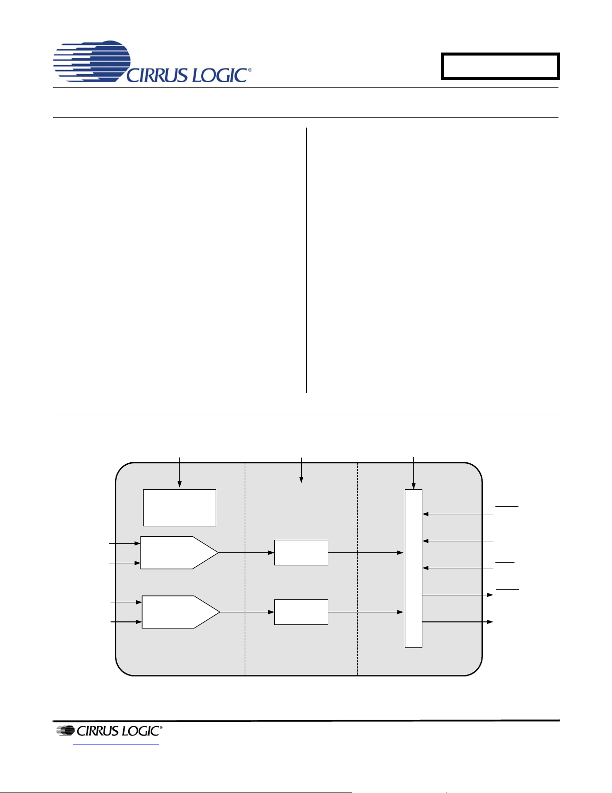
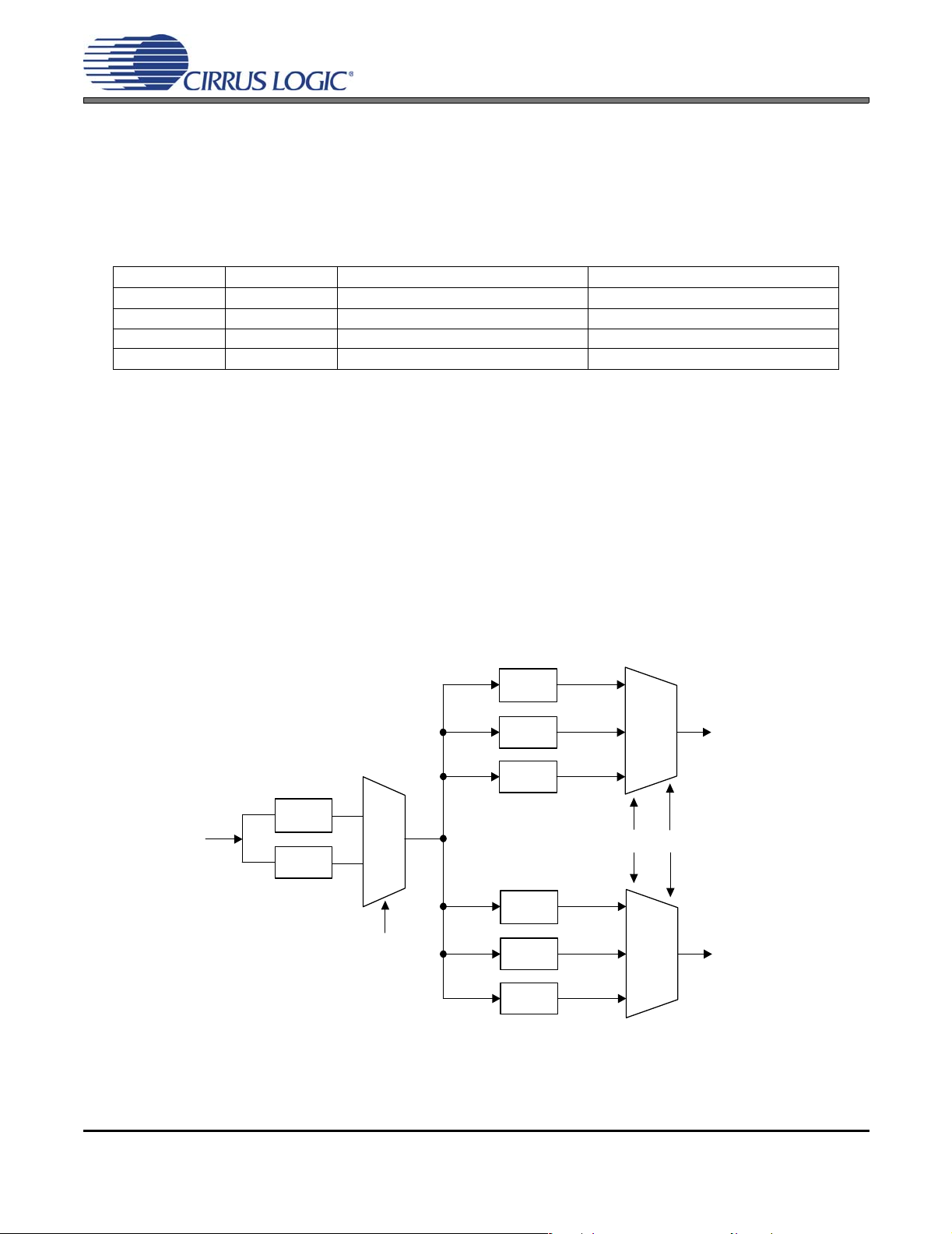
The CS5381 is a complete an alog-to-digital converter
for digital audio systems. It perfor ms sa mplin g, an alog to-digital conversion, and anti-alias filtering - generating
24-bit values for both left and right inputs in serial form
at sample rates up to 216 kHz per channel.
The CS5381 uses a 5th-order, multi-bit delta-sigma
modulator followed by digital filtering and decimation,
which removes the need for an external anti-alias filter.
The ADC uses a differential architecture which provides
excellent noise rejection.
The CS5381 is available in 24-pin TSSOP and SOIC
packages for Commercial grade (-10° to +70° C). The
CDB5381 Customer Demonstration board is also available for device evaluation and implementation
suggestions. Please refer to the “Ordering Information”
on page 22.
The CS5381 is ideal for audio systems requiring wide
dynamic range, negligible distortion, and low noise such as A/V receivers, DVD-R, CD-R, digital mixing
consoles, and effects processors.
Differential
Inputs
Differential
Inputs
http://www.cirrus.com
Analog Su p ply
5 V
Interna l Voltage
Reference
Switch-Cap
ADC
Switch-Cap
ADC
Digital Supply
3.3 V to 5 V
Digital
Filters
Digital
Filters
Copyright © Cirrus Logic, Inc. 2005
(All Rights Reserved)
Interfac e Supply
2.5 V to 5 V
Level Translator
Reset
Mode
Configuration
HPF
OVFL
PCM Serial
Audio Output
JULY '05
DS563F2

TABLE OF CONTENTS
1. PIN DESCRIPTIONS ............................................................................................................................... 4
2. CHARACTERISTICS AND SPECIFICATIONS....................................................................................... 5
SPECIFIED OPERATING CONDITIONS .................................................................................................... 5
ABSOLUTE MAXIMUM RATINGS............................................................................................................... 5
ANALOG CHARACTERISTICS (CS5381-KSZ/-KZZ).................................................................................. 6
DIGITAL FILTER CHARACTERISTICS........ ... ....................................... ... ... .... ... ... ... .... ... ........................... 7
SWITCHING CHARACTERISTICS - SERIAL AUDIO PORT .................................................................... 10
DC ELECTRICAL CHARACTERISTICS.................................................................................................... 13
DIGITAL CHARACTERISTICS ............................................................................ ... ... .... ... ... ... ... .... ............ 13
THERMAL CHARACTERISTICS .............................................................................................................. 13
TYPICAL CONNECTION DIAGRAM ......................................................................................................... 14
3. APPLICATIONS ............. ... .... ... ... ....................................... ... ... .... ... ...................................................... 15
3.1 Operational Mode/Sample Rate Range Select.............................................................................. 15
3.2 System Clocking............................................................................................................................ 15
3.2.1 Master Mode........................................................................................................................ 15
3.2.2 Slave Mode.......................................................................................................................... 16
3.3 Power-Up Sequence ..................................................................................................................... 16
3.4 Analog Connections ...................................................................................................................... 16
3.5 High-Pass Filter and DC Offset Calibration.................................................................................. 17
3.6 Overflow Detection ........................................................................................................................ 18
3.6.1 OVFL Configuration ............................................................................................................. 18
3.6.2 OVFL Output Timing ............................................................................................................ 18
3.7 Grounding and Power Supply Decoupling..................................................................................... 18
3.8 Synchronization of Multiple Devices.............................................................................................. 18
3.9 Capacitor Size on the Reference Pin (FILT+)................................................................................19
4. PACKAGE DIMENSIONS ........ ... ... .... ... ... ... ... ....................................... ... .... ... ... ... .... ... ... ...................... 20
5. ORDERING INFORMATION .............................................. ....................................... ... ... ... ... .... ............ 22
7. REVISION HISTORY....................................................................... ... ... ... ............................................. 24
CS5381
2 DS563F2

LIST OF FIGURES
Figure 1. Single-Speed Mode Stopband Rejection. . . . . . . . . . . . . . . . . . . . . . . . . . . . . . . . . . . . . . . . . . . 8
Figure 2. Single-Speed Mode Transition Band. . . . . . . . . . . . . . . . . . . . . . . . . . . . . . . . . . . . . . . . . . . . . . 8
Figure 3. Single-Speed Mode Transition Band (Detail). . . . . . . . . . . . . . . . . . . . . . . . . . . . . . . . . . . . . . . . 8
Figure 4. Single-Speed Mode Passband Ripple . . . . . . . . . . . . . . . . . . . . . . . . . . . . . . . . . . . . . . . . . . . . . 8
Figure 5. Double-Speed Mode Stopband Rejection . . . . . . . . . . . . . . . . . . . . . . . . . . . . . . . . . . . . . . . . . . 8
Figure 6. Double-Speed Mode Transition Band . . . . . . . . . . . . . . . . . . . . . . . . . . . . . . . . . . . . . . . . . . . . . 8
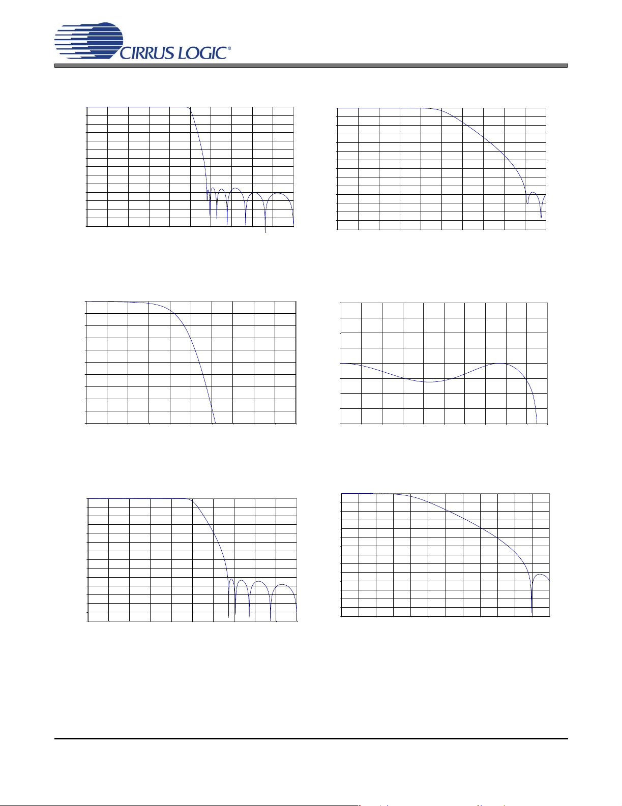
Figure 7. Double-Speed Mode Transition Band (Detail). . . . . . . . . . . . . . . . . . . . . . . . . . . . . . . . . . . . . . . 9
Figure 8. Double-Speed Mode Passband Ripple . . . . . . . . . . . . . . . . . . . . . . . . . . . . . . . . . . . . . . . . . . . . 9
Figure 9. Quad-Speed Mode Stopband Rejection . . . . . . . . . . . . . . . . . . . . . . . . . . . . . . . . . . . . . . . . . . . 9
Figure 10. Quad-Speed Mode Transition Band . . . . . . . . . . . . . . . . . . . . . . . . . . . . . . . . . . . . . . . . . . . . . 9
Figure 11. Quad-Speed Mode Transition Band (Detail) . . . . . . . . . . . . . . . . . . . . . . . . . . . . . . . . . . . . . . . 9
Figure 12. Quad-Speed Mode Passband Ripple . . . . . . . . . . . . . . . . . . . . . . . . . . . . . . . . . . . . . . . . . . . . 9
Figure 13. Master Mode, Left-Justified SAI. . . . . . . . . . . . . . . . . . . . . . . . . . . . . . . . . . . . . . . . . . . . . . . . 11
Figure 14. Slave Mode, Left-Justified SAI. . . . . . . . . . . . . . . . . . . . . . . . . . . . . . . . . . . . . . . . . . . . . . . . . 11
Figure 15. Master Mode, I²S SAI. . . . . . . . . . . . . . . . . . . . . . . . . . . . . . . . . . . . . . . . . . . . . . . . . . . . . . . . 11
Figure 16. Slave Mode, I²S SAI. . . . . . . . . . . . . . . . . . . . . . . . . . . . . . . . . . . . . . . . . . . . . . . . . . . . . . . . . 11
Figure 17. OVFL Output Timing . . . . . . . . . . . . . . . . . . . . . . . . . . . . . . . . . . . . . . . . . . . . . . . . . . . . . . . . 11
Figure 18. Left-Justified Serial Audio Interface . . . . . . . . . . . . . . . . . . . . . . . . . . . . . . . . . . . . . . . . . . . . . 12
Figure 19. I²S Serial Audio Interface. . . . . . . . . . . . . . . . . . . . . . . . . . . . . . . . . . . . . . . . . . . . . . . . . . . . . 12
Figure 20. OVFL Output Timing, I²S Format. . . . . . . . . . . . . . . . . . . . . . . . . . . . . . . . . . . . . . . . . . . . . . . 12
Figure 21. OVFL Output Timing, Left-Justified Format . . . . . . . . . . . . . . . . . . . . . . . . . . . . . . . . . . . . . . . 12
Figure 22. Typical Connection Diagram . . . . . . . . . . . . . . . . . . . . . . . . . . . . . . . . . . . . . . . . . . . . . . . . . . 14
Figure 23. CS5381 Master Mode Clocking . . . . . . . . . . . . . . . . . . . . . . . . . . . . . . . . . . . . . . . . . . . . . . . . 15
Figure 24. Recommended Analog Input Buffer. . . . . . . . . . . . . . . . . . . . . . . . . . . . . . . . . . . . . . . . . . . . . 17
Figure 25. CS5381 THD + N versus Frequency . . . . . . . . . . . . . . . . . . . . . . . . . . . . . . . . . . . . . . . . . . . . 19
CS5381
LIST OF TABLES
Table 1. CS5381 Mode Control. . . . . . . . . . . . . . . . . . . . . . . . . . . . . . . . . . . . . . . . . . . . . . . . . . . . . . . . . 15
Table 2. CS5381 Common Master Clock Frequencies. . . . . . . . . . . . . . . . . . . . . . . . . . . . . . . . . . . . . . . 16
Table 3. CS5381 Slave Mode Clock Ratios . . . . . . . . . . . . . . . . . . . . . . . . . . . . . . . . . . . . . . . . . . . . . . . 16
DS563F2 3
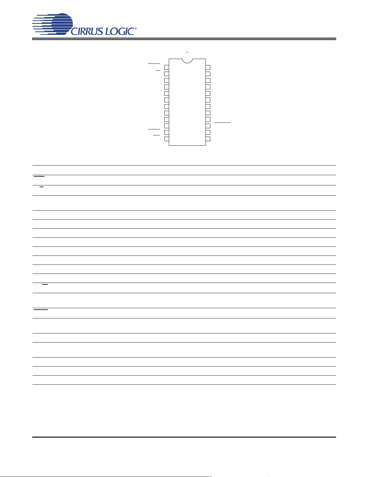
1. PIN DESCRIPTIONS
Pin Name # Pin Description
RST
M/S
LRCK
SCLK
MCLK
VD
GND
VL
SDOUT
MDIV
HPF
I²S/LJ
M0
M1
OVFL
AINL+
AINL-
VA
AINR-
AINR+
VQ
REF_GND
FILT+
13,14
16, 17
20, 21
1
2
3
4
5
6
7,18
8
9
10
11
12
15
19
22
23
24
Reset (Input) - The device enters a low power mode when low.
Master/Slave Mode (Input) - Selects operation as either clock master or slave.
Left Right Clock (Input/Output) - Determines which channel, Left or Right, is currently active on th e
serial audio data line.
Serial Clock (Input/Output) - Serial clock for the serial audio interface.
Master Clock (Input) - Clock source for the delta-sigma modulator and digital filters.
Digital Power (Input) - Positive power supply for the digital section.
Ground (Input) - Ground reference. Must be connected to analog ground.
Logic Power (Input) - Positive power for the digital input/output.
Serial Audio Data Output (Output) - Output for two’s complement serial audio data.
MCLK Divider (Input) - Enables a master clock divide by two function.
High-Pass Filter Enable (Input) - Enables the Digital High-Pass Filter.
Serial Audio Interface Format Select (Input) -Selects either the left-justified or I²S format for the SAI.
Mode Selection (Input) - Determines the operational mode of the device.
Overflow (Output, open drain) - Detects an overflow condition on both left and right channels.
Differential Left Channel Analog Inpu t (Input) - Signals are presented differentially to the delta-sigma
modulators via the AINL+/- pins.
Analog Power (Input) - Positive power supply for the analog section.
Differential Right Channel Analog Input (Input) -Signals are presented differentially to the delta-
sigma modulators via the AINR+/- pins.
Quiescent Voltage (Output) - Filter connection for the internal quiescent reference voltage.
Reference Ground (Input) - Ground reference for the internal sampling circuits.
Positive Voltage Reference (Output) - Positive reference voltage for the internal sampling circuits.
CS5381
RST 124FILT+
M/S 223REFGND
LRCK 322VQ
SCLK 421AINR+
MCLK 520AINR-
VD 619VA
GND 718GND
VL 817AINL-
SDOUT 916AINL+
MDIV 10 15 OVFL
HPF 11 14 M1
I²S/LJ 12 13 M0
4 DS563F2
CS5381
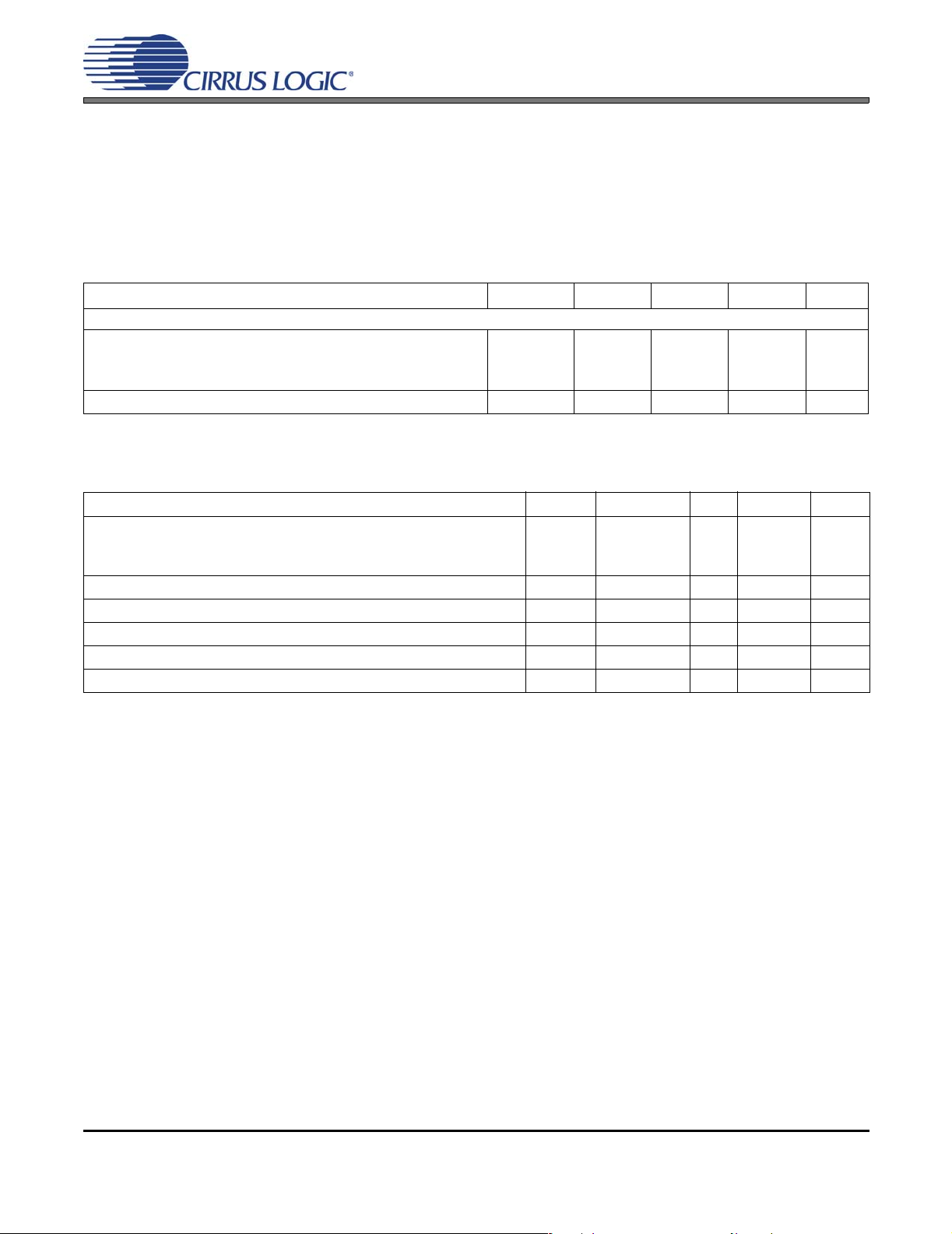
2. CHARACTERISTICS AND SPECIFICATIONS
All Min/Max characteristics and specifications are guaranteed over the Specified Operating Conditions. T ypical performance characteristics and specifications are derived from measurements taken at VA = 5.0 V, VD = VL = 3.3 V,
and TA = 25
°C.
SPECIFIED OPERATING CONDITIONS
(GND = 0 V; all voltages with respect to 0 V.)
Parameters Symbol Min Typ Max Units
DC Power Supply
DC Power Supplies: Positive Analog
Positive Digital
Positive Logic
Ambient Operating Temperature (Power Applied)
VA
VD
VL
T
4.75
3.1
2.37
A
-10 - +70 °C
5.0
-
-
5.25
5.25
5.25
V
V
V
ABSOLUTE MAXIMUM RATINGS
(GND = 0 V, All voltages with respect to ground.) (Note 1)
Parameter Symbol Min Typ Max Units
DC Power Supplies: Analog
Logic
Digital
Input Current (Note 2)
Analog Input Voltage (Note 3)
Digital Input Voltage (Note 3)
Ambient Operating Temperature (Power Applied)
Storage Temperature
V
T
VA
VL
VD
I
in
V
IND
T
stg
-0.3
-0.3
-0.3
-
-
-
+6.0
+6.0
+6.0
V
V
V
-10 - +10 mA
IN
GND-0.7 - VA+0.7 V
-0.7 - VL+0.7 V
A
-50 - +95 °C
-65 - +150 °C
Notes:
1. Operation beyond these limits may result in permanent damage to the device. Normal operation is not
guaranteed at these extremes.
2. Any pin except supplies. Transient currents of up to ±100 mA on the analog input pins will not cause
SRC latch-up.
3. The maximum over/under voltage is limited by the input current.
DS563F2 5
CS5381
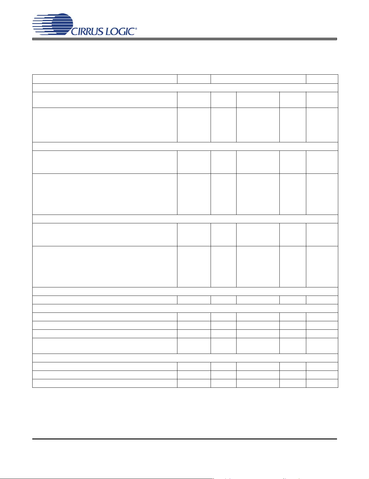
ANALOG CHARACTERISTICS (CS5381-KSZ/-KZZ)
Test conditions (unless otherwise specified): Input test signal is a 1 kHz sine wave; measurement bandwidth is
10 Hz to 20 kHz.
Parameter Symbol Min Typ Max Unit
Single-Speed Mode Fs = 48 kHz
Dynamic Range A-weighted
unweighted
Total Harmonic Distortion + Noise (Note 4)
-1 dB
-20 dB
-60 dB
Double-Speed Mode Fs = 96 kHz
Dynamic Range A-weighted
unweighted
40 kHz bandwidth unwei ghted
Total Harmonic Distortion + Noise (Note 4)
-1 dB
-20 dB
-60 dB
40 kHz bandwidth -1 dB
Quad-Speed Mode Fs = 192 kHz
Dynamic Range A-weighted
unweighted
40 kHz bandwidth unwei ghted
Total Harmonic Distortion + Noise (Note 4)
-1 dB
-20 dB
-60 dB
40 kHz bandwidth -1 dB
Dynamic Performance for All Modes
Interchannel Isolation
DC Accuracy
Interchannel Gain Mismatch
Gain Error
Gain Drift
Offset Error HPF enabled
HPF disabled
Analog Input Characteristics
Full-scale Input Voltage
Input Impedance (Differential) (Note 5)
Common Mode Rejection Ratio
THD+N
THD+N
THD+N
CMRR - 100 - dB
114
111
-
-
-
114
111
-
-
-
-
-
114
111
-
-
-
-
-
120
117
-110
-97
-57
120
117
114
-110
-97
-57
-107
120
117
114
-110
-97
-57
-107
-
-
-104
-
-
-
-
-
-104
-
-
-
-
-
-
-104
-
-
-
dB
dB
dB
dB
dB
dB
dB
dB
dB
dB
dB
dB
dB
dB
dB
dB
dB
dB
dB
-110-dB
-0.1-dB
-5 - 5 %
- ±100 - ppm/°C
-
-
0
100
-
-
LSB
LSB
1.07*VA 1.13*VA 1.18*VA Vpp
-2.5-kΩ
4. Referred to the typical full-scale input voltage.
5. Measured between AIN+ and AIN-.
6 DS563F2
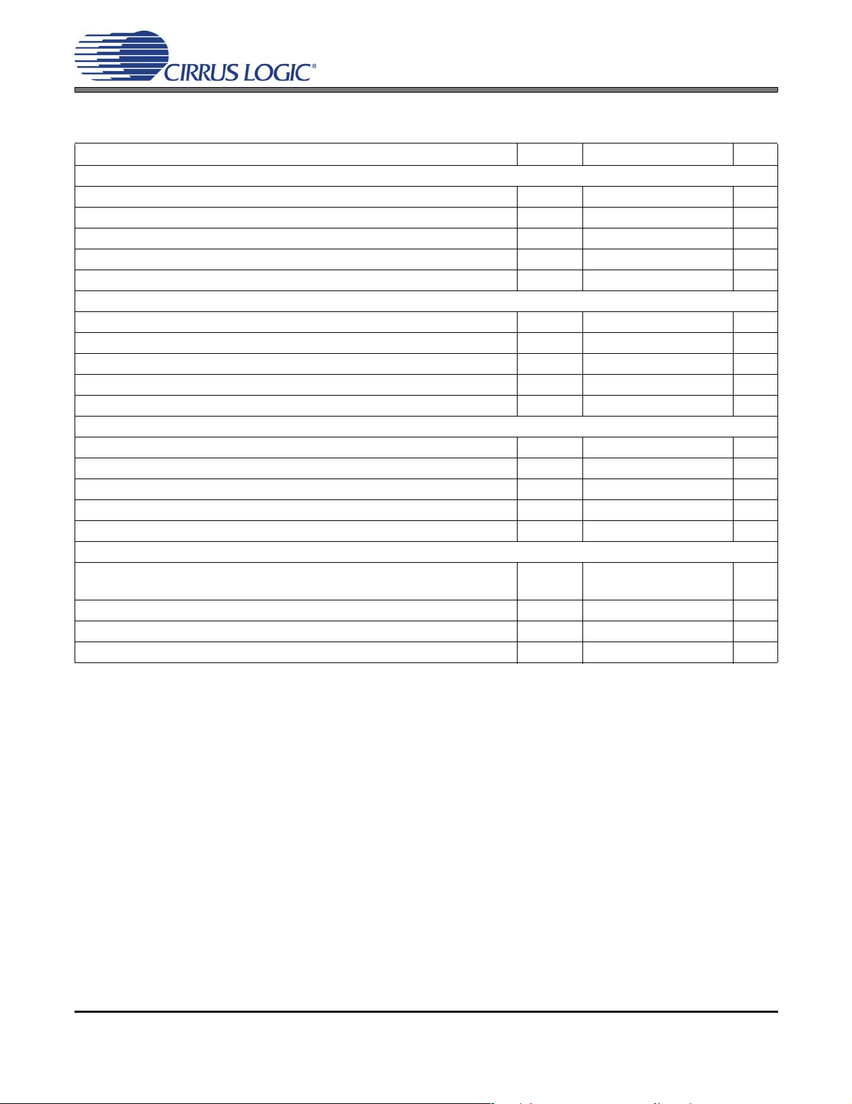
DIGITAL FILTER CHARACTERISTICS
Parameter Symbol Min Typ Max Unit
Single-Speed Mode (2 kHz to 54 kHz sample rates)
Passband (-0.1 dB) (Note 6)
Passband Ripple
Stopband (Note 6)
Stopband Attenuation
Total Group Delay (Fs = Output Sample Rate)
Double-Speed Mode (50 kHz to 108 kHz sample rates)
Passband (-0.1 dB) (Note 6)
Passband Ripple
Stopband (Note 6)
Stopband Attenuation
Total Group Delay (Fs = Output Sample Rate)
Quad-Speed Mode (100 kHz to 216 kHz sample rates)
Passband (-0.1 dB) (Note 6)
Passband Ripple
Stopband (Note 6)
Stopband Attenuation
Total Group Delay (Fs = Output Sample Rate)
High-Pass Filter Characteristics
Frequency Response -3.0 dB
-0.13 dB (Note 7)
Phase Deviation @ 20 Hz (Note 7)
Passband Ripple
Filter Setting Time
CS5381
0 - 0.47 Fs
-0.1 - 0.035 dB
0.58 - - Fs
-95 - - dB
t
gd
t
gd
t
gd
-12/Fs- s
0 - 0.45 Fs
-0.1 - 0.035 dB
0.68 - - Fs
-92 - - dB
-9/Fs- s
0 - 0.24 Fs
-0.1 - 0.035 dB
0.78 - - Fs
-97 - - dB
-5/Fs- s
-120-
-
Hz
Hz
-10-Deg
--0dB
105/Fs s
6. The filter frequency response scales precisely with Fs.
7. Response shown is for Fs equal to 48 kHz. Filter characteristics scale with Fs.
DS563F2 7
CS5381
0
-10
-20
-30
-40
-50
-60
-70
-80
Amplitude (dB)
-90
-100
-110
-120
-130
-140
0.00.10.20.30.40.50.60.70.80.91.0
Frequency (normalized to Fs)
0
-10
-20
-30
-40
-50
-60
-70
-80
Amplitude (dB)
-90
-100
-110
-120
-130
-140
0.40 0.42 0.44 0.46 0.48 0.50 0.52 0.54 0.56 0.58 0.60
Frequency (normalized to Fs)
Figure 1. Single-Speed Mode Stopband Rejection Figure 2. Single-Speed Mode Transition Band
0
-1
-2
-3
-4
-5
Amplitude (dB)
-6
-7
-8
-9
-10
0.45 0.46 0.47 0.48 0.49 0.50 0.51 0.52 0.53 0.54 0.55
Frequency (normalized to Fs)
0.10
0.08
0.05
0.03
0.00
Amplitude (dB)
-0.03
-0.05
-0.08
-0.10
0.00 0.05 0.10 0.15 0.20 0.25 0.30 0.35 0 .40 0.45 0.50
Frequency (normalized to Fs)
Figure 3. Single-Speed Mode Transition Band (Detail) Figure 4. Single-Speed Mode Passband Ripple
0
-10
-20
-30
-40
-50
-60
-70
-80
Amplitude (dB)
-90
-100
-110
-120
-130
-140
0.0 0.1 0.2 0.3 0.4 0.5 0.6 0.7 0.8 0.9 1.0
Frequency (normalized to Fs)
0
-10
-20
-30
-40
-50
-60
-70
-80
Amplitude (dB)
-90
-100
-110
-120
-130
-140
0.40 0.43 0.45 0.48 0.50 0.53 0.55 0.58 0.60 0.63 0.65 0.68 0.70
Frequency (normalized to Fs)
Figure 5. Double-Speed Mode Stopband Rejection Figure 6. Double-Speed Mode Transition Band
8 DS563F2
CS5381
0
-1
-2
-3
-4
-5
Amplitude (dB)
-6
-7
-8
-9
-10
0.40 0.43 0.45 0.48 0.50 0.53 0.55
Frequency (normalized to Fs)
Figure 7. Double-Speed Mode Transition Band (Detail) Figure 8. Double-Speed Mode Passband Ripple
0.10
0.08
0.05
0.03
0.00
Amplitude (dB)
-0.03
-0.05
-0.08
-0.10
0.00 0.05 0.10 0.15 0.20 0.25 0.30 0.35 0.40 0.45 0.50
Frequency (normalized to Fs)
0
-10
-20
-30
-40
-50
-60
-70
Amplitude (dB)
-80
-90
-100
-110
-120
0.0 0.1 0.2 0.3 0.4 0.5 0.6 0.7 0.8 0.9 1.0
Frequency (normalized to Fs)
0
-10
-20
-30
-40
-50
-60
-70
Amplitude (dB)
-80
-90
-100
-110
-120
-130
0.2 0.25 0.3 0.35 0.4 0.45 0.5 0.55 0.6 0 .65 0.7 0.75 0.8
Frequency (normalized to Fs)
Figure 9. Quad-Speed Mode Stopband Rejection Figure 10. Quad-Speed Mode Transition Band
0
-1
-2
-3
-4
-5
Amplitude (dB)
-6
-7
-8
-9
-10
0.10.150.20.250.30.350.40.450.50.550.6
Frequency (normalized to Fs)
0.10
0.08
0.06
0.04
0.02
0.00
Amplitude (dB)
-0.02
-0.04
-0.06
-0.08
-0.10
0.00 0.05 0.10 0.15 0.20 0.25
Frequency (normalized to Fs)
Figure 11. Quad-Speed Mode Transition Band (Detail) Figure 12. Quad-Speed Mode Passband Ripple
DS563F2 9

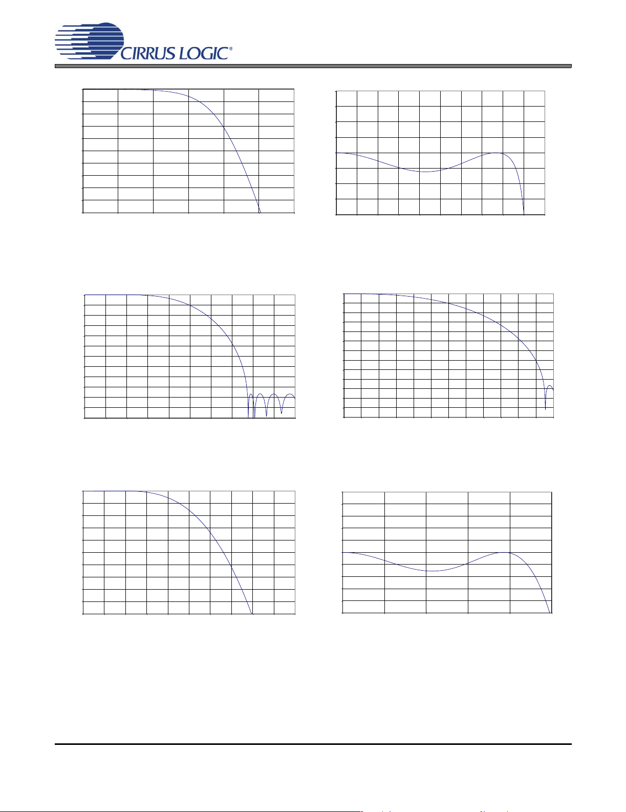
SWITCHING CHARACTERISTICS - SERIAL AUDIO PORT
(Logic “0” = GND = 0 V; Logic “1” = VL, CL = 20 pF)
Parameter Symbol Min Typ Max Unit
Output Sample Rate Single-Speed Mode
Double-Speed Mode
Quad-Speed Mode
OVFL to LRCK Edge Setup Time
OVFL to LRCK Edge Hold Time
OVFL time-out on overrange condition
Fs = 44.1, 88.2, 176.4 kHz
Fs = 48, 96, 192 kHz
MCLK Specifications
MCLK Period
MCLK Duty Cycle
Master Mode
SCLK falling to LRCK transition
SCLK falling to SDOUT valid
SCLK Duty Cycle
Slave Mode
Single-Speed
Output Sample Rate
LRCK Duty Cycle
SCLK Period
SCLK Duty Cycle
SDOUT valid before SCLK rising
SDOUT valid after SCLK rising
SCLK falling to LRCK transition
Double-Speed
Output Sample Rate
LRCK Duty Cycle
SCLK Period
SCLK Duty Cycle
SDOUT valid before SCLK rising
SDOUT valid after SCLK rising
SCLK falling to LRCK transition
Quad-Speed
Output Sample Rate
LRCK Duty Cycle
SCLK Period
SCLK Duty Cycle
SDOUT valid before SCLK rising
SDOUT valid after SCLK rising
SCLK falling to LRCK transition
Fs
Fs
Fs
t
setup
t
hold
100
16/f
1/f
2
50
sclk
sclk
-
-
t
clkw
36 - 1953 ns
40 - 60 %
t
mslr
t
sdo
-20 - 20 ns
- - 32 ns
-50-%
Fs 2 - 54 kHz
40 50 60 %
t
sclkw
145 - - ns
45 50 55 %
t
t
t
stp
hld
slrd
10 - - ns
5--ns
-20 - 20 ns
Fs 50 - 108 kHz
40 50 60 %
t
sclkw
145 - - ns
45 50 55 %
t
t
t
stp
hld
slrd
10 - - ns
5--ns
-20 - 20 ns
Fs 100 - 216 kHz
40 50 60 %
t
sclkw
72 - - ns
45 50 55 %
t
t
t
stp
hld
slrd
10 - - ns
5--ns
-8 - 8 ns
CS5381
-
-
-
--s
--s
740
680
54
108
216
-
-
kHz
kHz
kHz
ms
ms
10 DS563F2
CS5381
LRCK output
SCLK output
SDOUT
Figure 13. Master Mode, Left-Justified SAI Figure 14. Slave Mode, Left-Justified SAI
LRCK output
SCLK output
SDOUT
LRCK input
t
mslr
t
sdo
MSB MSB-1 MSB-2 MSB-3
SCLK input
SDOUT
t
slrd
t
stp
MSB
t
sclkh
t
hld
LRCK input
t
mslr
t
sdo
MSB MSB-1 MSB-2
MSB-3
SCLK input
SDOUT
t
slrd
t
sclkh
Figure 15. Master Mode, I²S SAI Figure 16. Slave Mode, I²S SAI
t
sclkl
t
sclkl
MSB-1
t
stp
MSB
t
hld
LRCK
t
setup
t
hold
OVFL
Figure 17. OVFL Output Timing
DS563F2 11

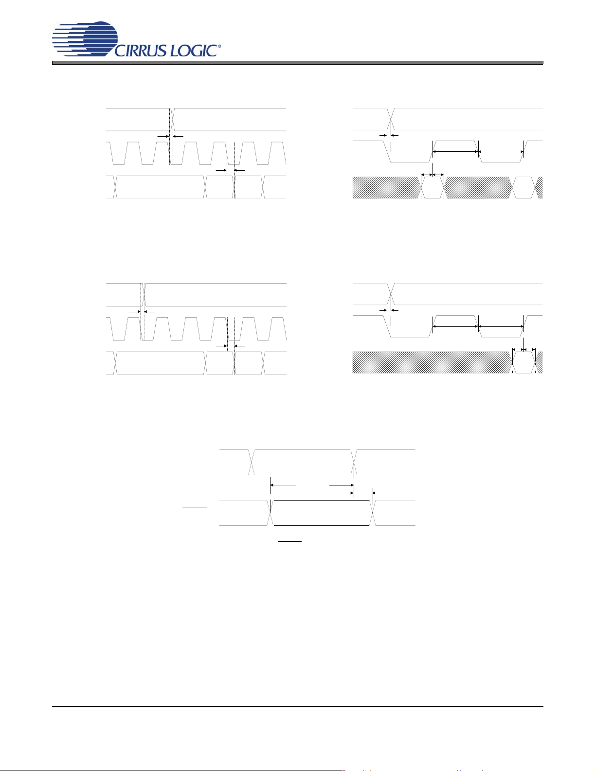
CS5381
LRCK
SCLK
SDATA 23 22 7 6 23 22
Left Channel Right Channel
23 225432108 7654321089 9
Figure 18. Left-Justified Serial Audio Interface
LRCK
SCLK
SDATA
22 8 7 23 22
23
Left Channel Right Channel
6543210 8765432109 9
22
23
Figure 19. I²S Serial Audio Interface
LRCK
Left Channel Frame
Right Channel Frame
SCLK
OVFL
LRCK
SCLK
OVFL
OVFL on Left Chan OVFL on Right Chan
Figure 20. OVFL Output Timing, I²S Format
Left Channel Frame
OV FL on R ight Chan
Figure 21. OVFL
Output Timing, Left-Justified Format
Right Channel Fram e
OV FL on Left
Chan
12 DS563F2

DC ELECTRICAL CHARACTERISTICS
(GND = 0 V, all voltages with respect to ground. MCLK=12.288 MHz; Master Mode)
Parameter Symbol Min Typ Max Unit
Power Supply Current VA = 5 V
(Normal Operation) VL,VD = 5 V
VL,VD = 3.3 V
Power Supply Current VA = 5 V
(Power-Down Mode) (Note 8) VL,VD = 5 V
Power Consumption
(Normal Operation) VA, VL, VD = 5 V
VA = 5 V; VL, VD = 3.3 V
(Power-Down Mode)
Power Supply Rejection Ratio (1 kHz) (Note 9)
VQ Nominal Voltage
Output Impedance
Maximum allowable DC current source/sink
Filt+ Nominal Voltage
Output Impedance
Maximum allowable DC current source/sink
I
A
I
D
I
D
I
A
I
D
-
-
-
-
-
-
-
-
-
-
-
PSRR - 65 - dB
-
-
-
-
-
-
36
36
24
100
100
360
260
1
2.5
25
0.01
5
4.5
0.01
43
46
28
-
-
445
307
-
-
-
-
-
-
-
CS5381
mA
mA
mA
uA
uA
mW
mW
mW
V
kΩ
mA
V
kΩ
mA
8. Power-Down Mode is defined as RST
= Low with all clocks and data lines held static.
9. Valid with the recommended capacitor values on FILT+ and VQ as shown in the Typical Connection
Diagram.
DIGITAL CHARACTERISTICS
Parameter Symbol Min Typ Max Units
High-Level Input Voltage (% of VL)
Low-Level Input Voltage (% of VL)
High-Level Output Voltage at Io = 100 µA (% of VL)
Low-Level Output Voltage at Io = 100 µA (% of VL)
OVFL Current Sink
Input Leakage Current
THERMAL CHARACTERISTICS
Parameter Symbol Min Typ Max Unit
Allowable Junction Temperature
Junction to Ambient Thermal Impedance
(Multi-layer PCB) TSSOP
(Multi-layer PCB) SOIC
(Single-layer PCB) TSSOP
(Single-layer PCB) SOIC
θ
JA-TM
θ
JA-SM
θ
JA-TS
θ
JA-SS
V
V
V
V
I
ovfl
OH
OL
I
IH
IL
in
70% - - V
--30%V
70% - - V
--15%V
--4.0mA
-10 - 10 µA
--135°C
-
-
-
-
70
60
105
80
-
-
-
-
°C/W
°C/W
°C/W
°C/W
DS563F2 13

TYPICAL CONNECTION DIAGRAM
CS5381
+5V
**47µF
+
+5 V to 3 .3 V
+
+
1µF
Analog
Input
Buffer
(Figure 24)
1µF
0.01µF
0.01µF
+ +
1µF 0.01
0.01µF
VA V
5.1
µF
*
0.01
0.01µF
µF
Ω
D
L
V
FILT+
REFGND
OVFL
VQ
2
I
RST
S/LJ
M/S
AINL+
CS5381
HPF
M0
M1
A/D CONVERTER
MDIV
AINL-
SDOUT
+5Vto 2.5 V
1µF
VL
10 k
Power Down
and Mode
Settings
Audio Data
Processor
Analog
Input
Buffer
(Figure 24)
AINR+
LRCK
SCLK
MCLK
TimingLogic
andClock
AINR-
* Resistor may only
be used if VD is
derived from VA. If
used, do not drive any
other logic from VD.
GND
Figure 22. Typical Connection Diagram
GND
** Capacitor value
affects low frequency
distortion. See
Section 3.9.
14 DS563F2
3. APPLICATIONS
3.1 Operational Mode/Sample Rate Range Select
The output sample rate, Fs, can be adjusted from 2 kHz to 216 kHz. The CS5381 must be set to the proper
speed mode via the mode pins, M1 and M0. Refer to Table 1.
M1 (Pin 14) M0 (Pin 13 ) MODE Output Sample Rate (Fs)
00
01
10
11
3.2 System Clocking
The device supports operation in either Master Mode, where the left/right and serial clocks are synchronously generated on-chip, or Slave Mode, which requires external generation of the left/right and serial clocks.
The device also includes a master clock divider in Master Mode where the master clock will be internally
divided prior to any other internal circuitry when MDIV is enabled, set to logic 1. In Slave Mode, the MDIV
pin needs to be disabled, set to logic 0.
Single-Speed Mode 2 kHz - 54 kHz
Double-Speed Mode 50 kHz - 108 kHz
Quad-Speed Mode 100 kHz - 216 kHz
Reserved
Table 1. CS5381 Mode Control
CS5381
3.2.1 Master Mode
In Master mode, LRCK and SCLK operate as outputs. The left/right and serial clocks are inter nally derived
from the master clock with the left/right clock equal to Fs and the serial clock equal to 64x Fs, as shown
in Figure 23. Refer to Table 2 for common master clock frequencies.
MCLK
÷ 1
÷ 2
0
1
MDIV
÷ 256
÷ 128
÷ 64
÷ 4
÷ 2
÷ 1
Single
Speed
Double
Speed
Quad
Speed
Single
Speed
Double
Speed
Quad
Speed
00
01
10
00
01
10
LRCK Output
(Equal to Fs)
M0M1
SCLK Output
Figure 23. CS5381 Master Mode Clocking
DS563F2 15
CS5381
SAMPLE RATE (kHz)
3.2.2 Slave Mode
LRCK and SCLK operate as inputs in Slave mode. It is recommended that the left/right clock be synchronously derived from the master clock and must be equal to Fs. It is a lso recommended that the serial clock
be synchronously derived from the master clock and be equal to 64x Fs to maximize system performance.
Refer to Table 3 for required clock ratios.
MCLK/LRCK Ratio
SCLK/LRCK Ratio
* Only available in Master mode.
MDIV = 0
MCLK (MHz)
32 8.192 16.384
44.1 11.2896 22.5792
48 12.288 24.576
64 8.192 16.384
88.2 11.2896 22.5792
96 12.288 24.576
176.4 11.2896 22.5792
192 12.288 24.576
Table 2. CS5381 Common Master Clock Frequencies
Single-Speed Mode
Fs = 2 kHz to 54 kHz
256x, 512x 128x, 256x 64x*, 128x
64x, 128x 64x 64x
Double-Speed Mode
Fs = 50 kHz to 108 kHz
MDIV = 1
MCLK (MHz)
Quad-Speed Mode
Fs = 100kHz to 216kHz
3.3 Power-Up Sequence
Reliable power-up can be accomplished by keeping the device in reset until the power supplies, clocks and
configuration pins are stable. It is also recommended that reset be enabled if the analog or digital supplies
drop below the minimum specified operating voltages to prevent power glitch related issues.
The internal reference voltage must be stable for the de vice to produ ce valid data. Ther efore, there is a delay between the release of reset and the generation of valid output, due to the finite output impedance of
FILT+ and the presence of the external capacitance. This dura tion of this de lay is less than 2500 LRCK cycles.
3.4 Analog Connections
The analog modulator samples the input at 6.144 MHz . The digital filter will reject signals within the stopband of the filter. However, there is no rejection for input signals which are (n
band frequency, where n=0,1,2,... Refer to Figure 24, which shows the suggested filter that will attenuate
any noise energy at 6.144 MHz in addition to providing the optimum source impedance for the modulators.
The use of capacitors which have a large voltage coefficient (such as general purpose ceramics) must be
avoided since these can degrade signal linearit y . C0G capacitors are recommended for this application.
Table 3. CS5381 Slave Mode Clock Ratios
× 6.144 MHz) the digital pass-
16 DS563F2
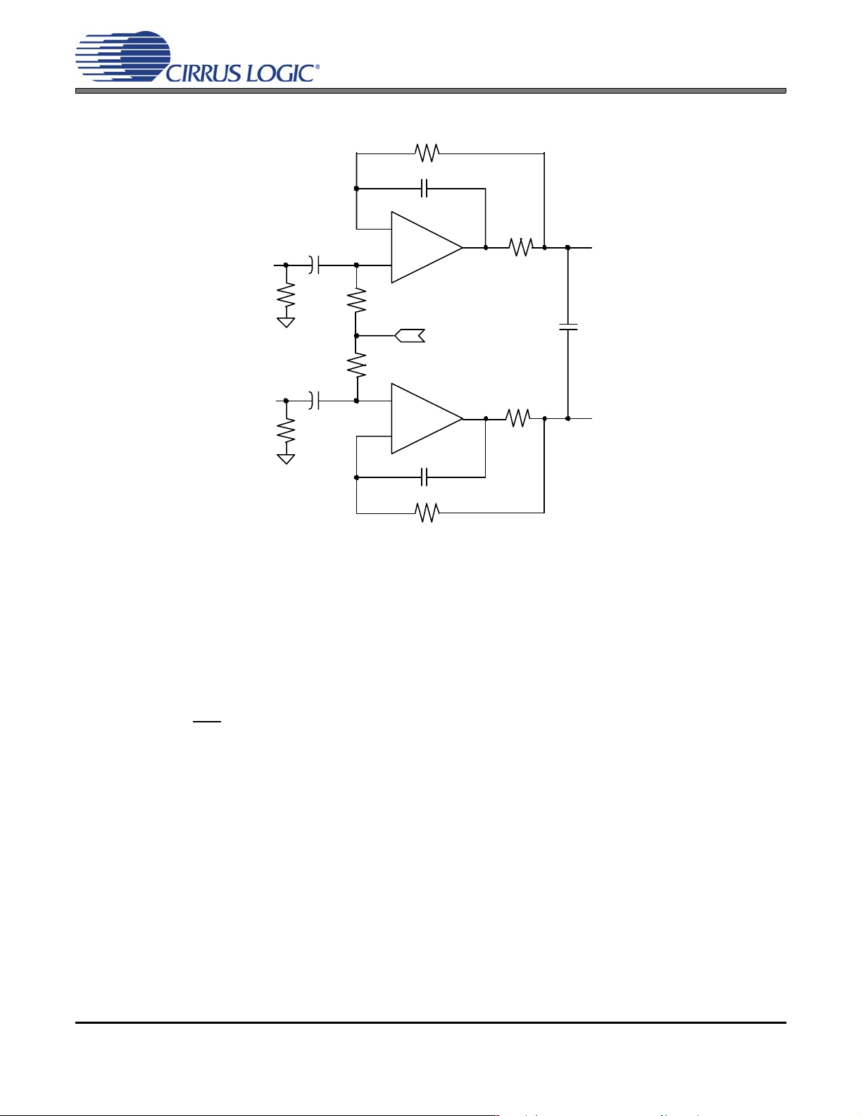
634 Ω
CS5381
470 pF
COG
-
10 uF
kΩ
10
10kΩ
+
VQ
+
-
470 pF
COG
634 Ω
AIN+
100
AIN-
100
Ω
k
10 uF
Ω
k
Figure 24. Recommended Analog Input Buffer
3.5 High-Pass Filter and DC Offset Calibration
The operational amplifiers in the input circuitry driving the CS5381 may generate a small DC offset into the
A/D converter. The CS5381 includes a high-pass filter after the decimator to remove any D C offset w hich
could result in recording a DC level, possibly yielding “clicks” when switching between devices in a multichannel system.
91 Ω
ADC AIN+
COG
2700 pF
91 Ω
ADC AIN-
The high-pass filter continuou sly subtracts a measure of th e DC offset from the output of the decimation
filter. If the HPF
pin is taken high during normal operation, the current value of the DC offset registe r is frozen
and this DC offset will continue to be subtracted from the conversion result. This feature makes it possible
to perform a system DC offset calibration by:
1. Running the CS5381 with the high-pass filter enabled until the filter settles. See the Digital Filter Char-
acteristics for filter settling time.
2. Disabling the high-pass filter and freezing the stored DC offset.
A system calibration performed in this way will eliminate offsets anywhere in the signal path between the
calibration point and the CS5381.
DS563F2 17
3.6 Overflow Detection
The CS5381 includes overflow detection on both the left and right chann els. This time multip lexed information is presented as open drain, active low on pin 15, OVFL
logical low as soon as an overrange condition in the opposite channel is detected. The data will remain low
as specified in the “Switching Characteristics - Serial Audio Port” section on page 10. This ensures sufficient
time to detect an overrange condition regardless of the speed mode. After the timeout, the OVFL_L and
OVFL_R data will return to a logical high if there has not been any other overrange condition detected.
Please note that an overrange condition on either channel will restart the timeout period for both channels.
3.6.1 OVFL Configuration
If the system does not require overflow detection, the user may leave the OVFL pin disconnected. When
using the overflow detection capability of the CS5381, a 10 kΩ pull-up resistor must be inserted between
the OVFL
is high impedance for the case of no overflow condition, but the pull-up resistor will pull the node to VL.
When an overflow condition occurs, the OVFL
of the overflow condition. In effect, the user can use the OVFL
nel with an external circuit or a DSP. Furthermore, because the OVFL
of multiple CS5381 devices can be tied together such that an overflow condition on a single device will
drive the line low. When connecting OVFL
necessary.
pin and VL because the OVFL output is open drain, active low. This means that the OVFL pin
CS5381
. The OVFL_L and OVFL_R data will go to a
pin can drive the node to GND thus indicating the presence
pin to illuminate an LED, or mute the chan-
output is open-drain, the OVFL pins
pins of multiple devices, only a single 10kΩ pull-up resistor is
3.6.2 OVFL Output Timing
In left-justified format, the OVFL pin is updated one SCLK period after an LRCK transition. In I²S format,
the OVFL
cases, the OVFL
format, the rising edge of LRCK would latch the right channel overflow status, and the falling edge of
LRCK would latch the left channel overflow status. In I²S format, the falling edge of LRCK would latch the
right channel overflow status and the rising edge of LRCK would latch the left channel overflow status.
pin is updated two SCLK periods after an LRCK transition. Refer to Figures 20 and 21. In both
data can be easily demultiplexed by using the LRCK to latch the data. In left-justified
3.7 Grounding and Power Supply Decoupling
As with any high resolution converter, the CS5381 requires care ful attention to power supply and gro unding
arrangements if its potential performance is to be realized. Figure 22 shows the recommended power arrangements, with VA and VL connected to clean supplies. VD, which powers the digital filter, may be run
from the system logic supply or may be powered from the analog supply via a resistor. In this case, no additional devices should be powered from VD. Decoupling capacitors should be as near to the ADC as possible, with the low value ceramic capacitor being the nearest. All signals, especially clocks, should be kept
away from the FILT+ and VQ pins in order to avoid unwanted coupling into the modulators. The FILT+ and
VQ decoupling capacitors, particularly the 0.01 µF, must be positioned to minimize the electrical path from
FILT+ and REFGND. The CDB5381 evaluation board demonstrates the optimum layout and power supply
arrangements. To minimize digital noise, connect the ADC digital outputs only to CMOS inputs.
3.8 Synchronization of Multiple Devices
In systems where multiple ADCs are required, care must be taken to achieve simultaneous sampling. To
ensure synchronous sampling, the MCLK and LRCK must be the same for all of the CS5381’s in the system.
If only one master clock source is needed, one solution is to place one CS5381 in Master mode , and slave
all of the other CS5381’s to the one master. If multiple master clock sources ar e needed, a possible solution
would be to supply all clocks from the same external source and time the CS5381 reset with the falling edge
of MCLK. This will ensure that all converters begin sampling on the same clock edge.
18 DS563F2

3.9 Capacitor Size on the Reference Pin (FILT+)
The CS5381 requires an external capacitance on the internal reference voltage pin, FILT+. The size of this
decoupling capacitor will affect the low frequency distortion performance as shown in Figure 25, with larger
capacitor values used to optimize low frequency distortion performance. The THD+N curves in Figure 25
were measured with VA=VD=VL=5 V in Single-Speed Master Mode with a full-scale sinewave input.
1 uF
10 uF
22 uF
CS5381
47 uF
100 uF
220 uF
Figure 25. CS5381 THD + N versus Frequency
DS563F2 19
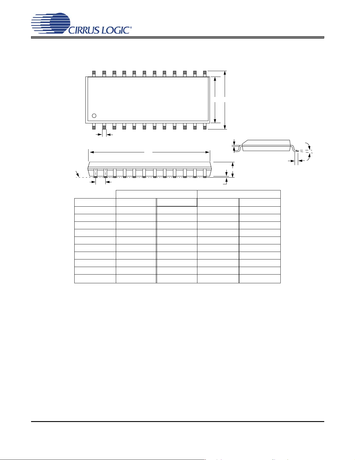
4. PACKAGE DIMENSIONS 24L SOIC (300 MIL BODY) PACKAGE DRAWING
1
b
CS5381
HE
c
SEATING
PLANE
D
A
e
A1
INCHES MILLIMETERS
DIM MIN MAX MIN MAX
A 0.093 0.104 2.35 2.65
A1 0.004 0.012 0.10 0.30
B 0.013 0.020 0.33 0.51
C 0.009 0.013 0.23 0.32
D 0.598 0.614 15.20 15.60
E 0.291 0.299 7.40 7.60
e 0.040 0.060 1.02 1.52
H 0.394 0.419 10.00 10.65
L 0.016 0.050 0.40 1.27
∝
0° 8° 0° 8°
∝
L
20 DS563F2
CS5381
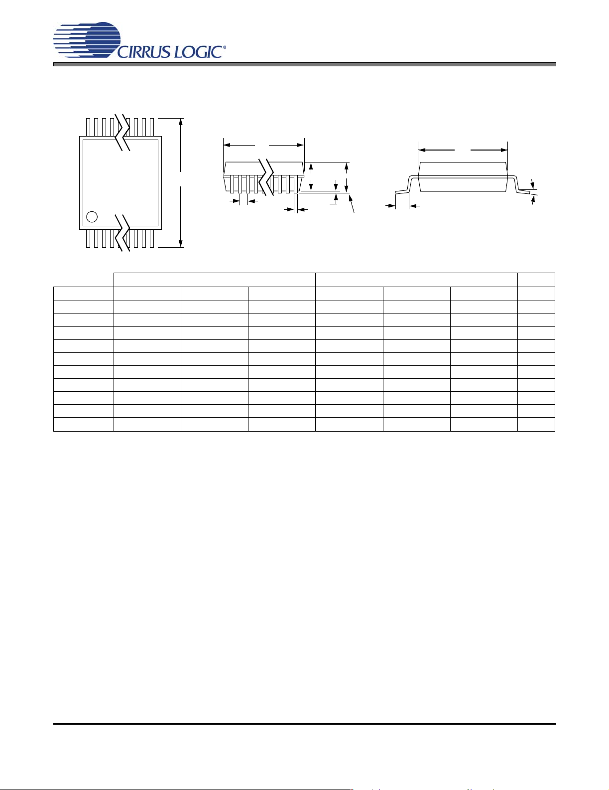
24L TSSOP (4.4 mm BODY) PACKAGE DRAWING
N
1
23
TOP VIEW
D
E
e
2
b
SIDE VIEW
A2
A1
A
SEATING
PLANE
L
1
E1
END VIEW
INCHES MILLIMETERS NOTE
DIM MIN NOM MAX MIN NOM MAX
A -- -- 0.043 -- -- 1.10
A1 0.002 0.004 0.006 0.05 -- 0.15
A2 0.03346 0.0354 0.037 0.85 0.90 0.95
b 0.00748 0.0096 0.012 0.19 0.245 0.30 2,3
D 0.303 0.307 0.311 7.70 7.80 7.90 1
E 0.248 0.2519 0.256 6.30 6.40 6.50
E1 0.169 0.1732 0.177 4.30 4.40 4.50 1
e -- 0.026 BSC -- -- 0.65 BSC --
L 0.020 0.024 0.028 0.50 0.60 0.70
µ
0° 4° 8° 0° 4° 8°
∝
Notes:
JEDEC #: MO-153
Controlling Dimension is Millimeters.
1. “D” and “E1” are reference datums and do not included mold flash or protrusions, but do include mold
mismatch and are measured at the parting line, mold flash or protrusions shall not exceed 0.20 mm per
side.
2. Dimension “b” does not include dambar protrusion/intrusion. Allowable dambar protrusion shall be
0.13 mm total in excess of “b” dimension at maximum material condition. Dambar intrusion shall not reduce dimension “b” by more than 0.07 mm at least material condition.
3. These dimensions apply to the flat section of the lead between 0.10 and 0.25 mm from lead tips.
DS563F2 21
5. ORDERING INFORMATION
CS5381
Product Description Package Pb-Free Grade Temp
Container Order #
Range
CS5381
CS5381
CDB5381 CS5381 Evaluation Board - - - - - CDB5381
120 dB, 192 kHz, Multi-Bit
Audio A/D Converter
120 dB, 192 kHz, Multi-Bit
Audio A/D Converter
24-TSSOP Yes Commercial -10° to +70° C
24-SOIC Yes Commercial -10° to +70° C
Bulk CS5381-KZZ
Tape & Reel CS5381-KZZR
Bulk CS5381-KSZ
Tape & Reel CS5381-KSZR
22 DS563F2

6 PARAMETER DEFINITIONS
Dynamic Range
The ratio of the rms value of the signal to the rms sum of all other spectral components over the specified
bandwidth. Dynamic Range is a signal-to-noise ratio measurement over the specified bandwidth made with
a -60 dBFS signal. 60 dB is added to resulting measurement to refer the measurement to full-scale. This
technique ensures that the distortion components ar e below the n oise level an d do n ot affect the m easu rement. This measurement technique has been accepted by the Audio Engineering Society, AES17-1991,
and the Electronic Industries Association of Japan, EIAJ CP-307. Expressed in decibels.
Total Harmonic Distortion + Noise
The ratio of the rms value of the signal to the rms sum of all other spectral components over the specified
bandwidth (typically 10 Hz to 20 kHz), including distortion components. Expressed in decibels. Measured
at -1 and -20 dBFS as suggested in AES17-1991 Annex A.
Frequency Response
A measure of the amplitude response variation from 10 Hz to 20 kHz relative to the amplitude response at
1 k Hz. Units in decibels.
Interchannel Isolation
A measure of crosstalk between the left and right channels. Measured for each channel at the conver ter's
output with no signal to the input under test and a full-scale signal applied to the other channel. Un its in decibels.
CS5381
Interchannel Gain Mismatch
The gain difference between left and right channels. Units in decibels.
Gain Error
The deviation from the nominal full-scale analog input for a full-scale digital output.
Gain Drift
The change in gain value with temperature. Units in ppm/°C.
Offset Error
The deviation of the mid-scale transition (111...111 to 000...000) from the ideal. Units in mV.
DS563F2 23

7. REVISION HISTORY
Release Date Changes
A1 December 2002
A2 October 2003
A3 May 2004
A4 August 2004
F1 July 2005
F2 July 2005
Initial Release
Changed front page description of digital filter
Improved distortion specification from -105 dB to -110 dB
Modified serial port timing specifications for slave mode operation
Added pull-down resistors to recommended input buffer
Changed full-scale voltage specification to reflect VA supply voltage
Added Applications section about capacitor value on FILT+ pin
Changed input impedance specification from 37 to 2.5 kΩ
Changed impedance specification on FILT+ from 35 to 4.5 kΩ
Add Lead free part number
Replaced diagrams showing OVFL functionality (see Figures 20 and 21)
Replaced Figures 13, 15, 18 and 19 to demonstrate pre-emption of the MSB.
Increased maximum digital current (I
) specification at 5 V from 43 mA to 46 mA. .
D
Updated Ordering Information.
CS5381
Contacting Cirrus Logic Support
For all product questions and inquiries contact a Cirrus Logic Sales Representative.
To find the one nearest to you go to www.cirrus.com
IMPORTANT NOTICE
Cirrus Logic, Inc. and its subsidiaries ("Cirrus") believe that the information contained in this document is accurate and reliable. However, the information is subject
to change without not ice and is pr ovided "AS IS" witho ut warr anty of any kind (express or implied). Customers are advised to obtain the latest version of relevant
information to verify, before placing orders, that information being relied on is current and complete. All products are sold subject to the terms and conditions of sale
supplied at the time of order acknowledgment, including those pertaining to warranty, indemnification, and limitation of liability. No responsibility is assumed by Cirrus
for the use of this information, including use of this information as the basis for manufacture or sale of any items, or for infringement of patents or other rights of third
parties. This document is the property of Cirrus and by furnishing this information, Cirrus grants no license, express or implied under any patents, mask work rights,
copyrights, trademarks, trade secrets or other inte llectual property rig hts. Cirrus owns the copyrights associated with the information contained herein and gives consent for copies to be made of the information only for use within your organization with respect to Cirrus integrated circuits or other products of Cirrus. This consent
does not extend to other copying such as copying for general distribution, advertising or promotional purposes, or for creating any work for resale.
CERTAIN APPLICATIONS USING SEMICONDUCTOR PRODUCTS MAY INVOLVE POTENTIAL RISKS OF DEATH, PERSONAL INJURY, OR SEVERE PROPERTY OR ENVIRONMENTAL DAMAGE (“CRITICAL APPLICATIONS”). CIRRUS PRODUCTS ARE NOT DESIGNED, AUTHORIZED OR WARR ANTED FOR USE
IN AIRCRAFT SYSTEMS, MILITARY APPLICATIONS, PRODUCTS SURGICALLY IMPLANTED INTO THE BODY, AUTOMOTIVE SAFETY OR SECURITY DEVICES, LIFE SUPPORT PRODUCTS OR OTHER CRITICAL APPLICATIONS. INCLUSION OF CIRRUS PRODUCTS IN SUCH APPLICATIONS IS UNDERSTOOD
TO BE FULLY AT THE CUSTOMER’S RISK AND CIRRUS DISCLAIMS AND MAKES NO WARRANTY, EXPRESS, STATUTO RY OR IMPL IED, INCLUDING THE
IMPLIED WARRANTIES OF MERCHANTABILITY AND FITNESS FOR PARTICULAR PURPOSE, WITH REGARD TO ANY CIRRUS PRODUCT THAT IS USED
IN SUCH A MANNER. IF THE CUSTOMER OR CUSTOMER’S CUSTOMER USES OR PERMITS THE USE OF CIRRUS PRODUCTS IN CRITICAL APPLICATIONS, CUSTOMER AGREES, BY SUCH USE, TO FULLY INDEMNIFY CIRRUS, ITS OFFICERS, DIRECTORS, EMPLOYEES, DISTRIBUTORS AND OTHER
AGENTS FROM ANY AND ALL LIABILITY, INCLUDING ATTORNEYS’ FEES AND COSTS, THAT MAY RESULT FROM OR ARISE IN CONNECTION WITH
THESE USES.
Cirrus Logic, Cirrus, and the Cirrus Logic logo design s ar e tra de m a rks of Ci rru s Lo gi c, Inc. All o ther bra nd and product names in this document may be trademarks
or service marks of their respective owners.
24 DS563F2
 Loading...