

CS5371
CS5372
Low-power, High-performance
Features & Description
z Fourth-order ∆Σ Architecture
z Clock-jitter-tolerant Architecture
z Input Voltage: 5 V
z High Dynamic Range
127 dB SNR @ 215 Hz BW (2 ms Output)
124 dB SNR @ 430 Hz BW (1 ms Output)
z Low Total Harmonic Distortion
-118 dB THD Typical, -112 dB THD Maximum
z Low Power Consumption
Normal Mode: 25 mW per Channel
Low-power Mode: 15 mW per Channel
z Small Footprint, 24-pin SSOP Package
z Single- or Multi-channel System Support
1-channel System: CS5371
2-channel System: CS5372
3-channel System: CS5371 + CS5372
4-channel System: CS5372 + CS5372
z Single or Dual Power Supply Configurations
VA+ = +5 V; VA- = 0 V; VD = +3.3 V to +5 V
VA+ = +2.5 V;VA- = -2.5 V;VD = +3.3 V
Fully Differential
pp
∆Σ
Modulators
Description
The CS5371 and CS5372 are one- and two-channel,
high dynamic range, fourth-order ∆Σ modulators intended for geophysical and sonar applications. Used in
combination with the CS5376A or CS5378 digital filters,
a unique high-resolution A/D measurement system
results.
The CS5371 and CS5372 have high dynamic range
(127 dB @ 215 Hz bandwidth) and low total harmonic
distortion (typically -118 dB THD), with very low power
consumption per channel. In normal mode
(LPWR=0, MCLK=2.048MHz), power consumption is
25 mW per channel, and in low-power mode
(LPWR=1, MCLK=1.024MHz), power consumption is
15 mW per channel. Each modulator can be independently powered down to 1 mW per channel, and by
halting the input clock, they will enter a micropower state
using only 10 µW per channel.
The modulators generate an oversampled serial bit
stream at 512 kbits per second when operated from a
clock frequency of 2.048 MHz. They are available in a
small 24-pin SSOP package, providing exceptional performance in a very small footprint.
ORDERING INFORMATION
See page 21.
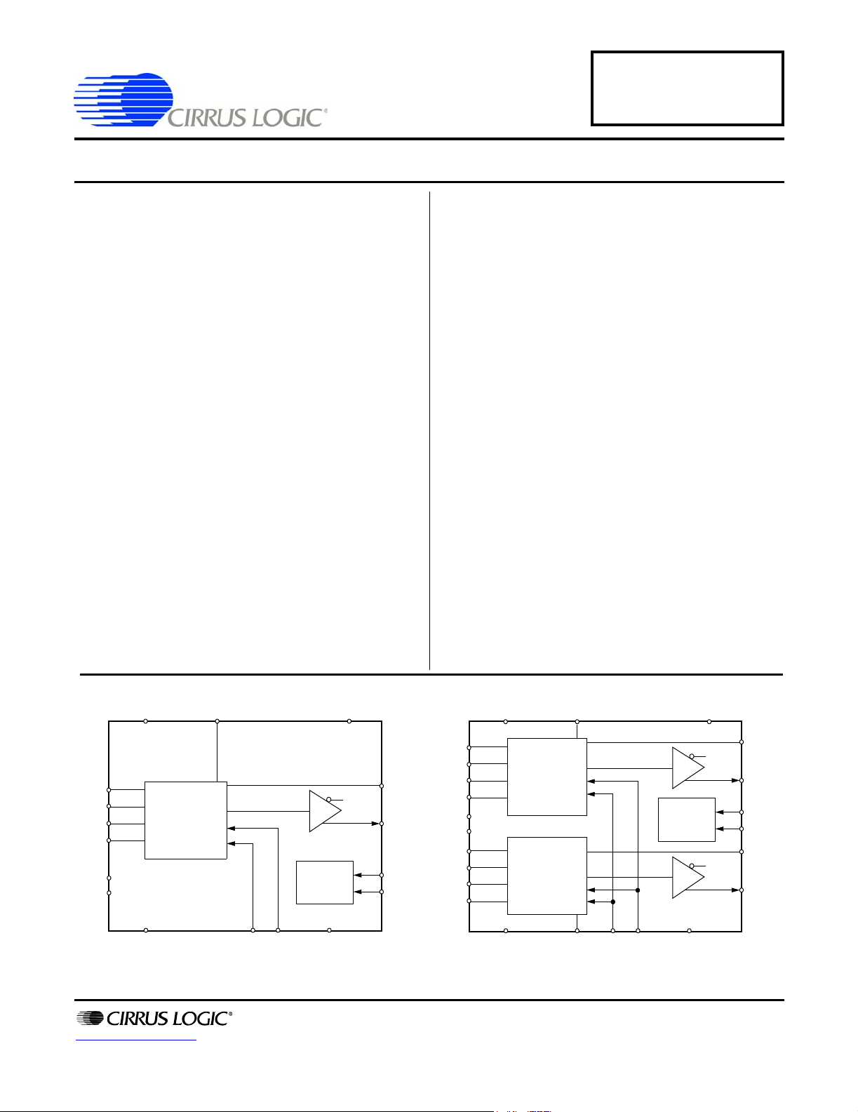
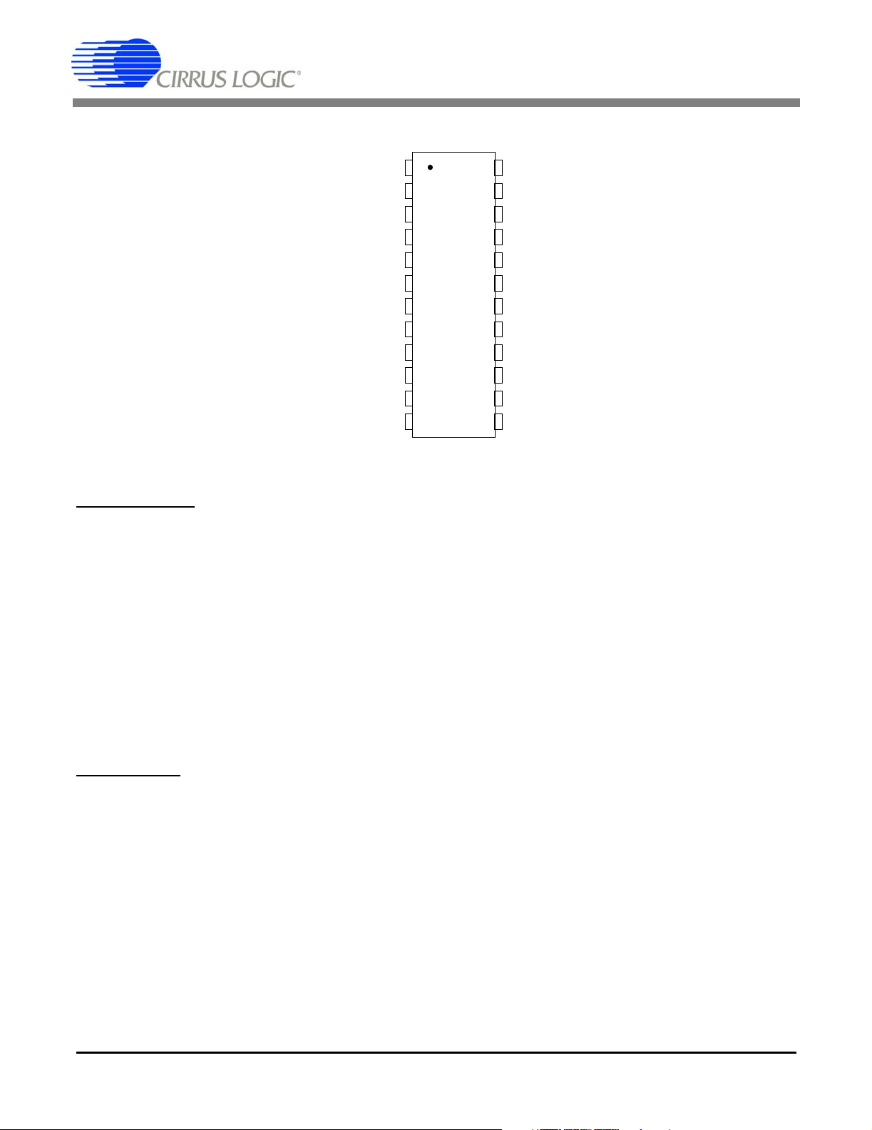
VA+
INF+
INR+
INRINF-
VREF+
VREF-
4TH ORDER
∆−Σ
MODULATOR
CS5371
VA-
http://www.cirrus.com
PWDN
OFST LPWR DGND
VD
MFLAG
MDATA
CLOCK
GENERATOR
Copyright © Cirrus Logic, Inc. 2005
MCLK
MSYNC
(All Rights Reserved)
INF1+
INR1+
INR1INF1-
VREF+
VREF-
INF2+
INR2+
INR2INF2-
VA+
VA-
4TH ORDER
∆−Σ
MODULATOR
4TH ORDER
∆−Σ
MODULATOR
PWDN1
PWDN2
OFST LPWR DGND
VD
CLOCK
GENERATOR
CS5372
MFLAG1
MDATA1
MCLK
MSYNC
MFLAG2
MDATA2
OCT ‘05
DS255F3

TABLE OF CONTENTS
1. CHARACTERISTICS & SPECIFICATIONS ................................................... 3
ANALOG CHARACTERISTICS .................................................................. 3
DIGITAL CHARACTERISTICS ................................................................... 5
ABSOLUTE MAXIMUM RATINGS ............................................................. 5
SWITCHING CHARACTERISTICS ............................................................ 6
2. GENERAL DESCRIPTION. ........................................................................... 7
3. MODULATOR PERFORMANCE ................................................................... 9
3.1. Full-scale Signal Performance ........................................................... 9
3.2. Noise Performance ............................................................................ 9
4. SIGNAL INPUTS ........................................................................................... 9
4.1. Differential Inputs - INR+/-, INF+/- ..................................................... 9
4.2. Anti-alias Filters ............................................................................... 10
4.3. Input Impedance .............................................................................. 10
4.4. Maximum Signal Levels ................................................................... 10
5. INPUT OFFSET ........................................................................................... 10
5.1. Offset Enable - OFST ...................................................................... 11
5.2. Offset Drift........................................................................................ 11
6. VOLTAGE REFERENCE INPUTS .............................................................. 11
6.1. Voltage Reference Configurations ................................................... 12
6.2. VREF Input Impedance.................................................................... 12
6.3. Gain Accuracy.................................................................................. 12
6.4. Gain Drift.......................................................................................... 12
7. DIGITAL FILTER INTERFACE ................................................................... 12
7.1. Modulator Clock - MCLK.................................................................. 13
7.2. Modulator Data - MDATA................................................................. 13
7.3. Modulator Sync - MSYNC................................................................ 13
7.4. Modulator Flag - MFLAG ................................................................. 13
8. POWER MODES ......................................................................................... 14
8.1. Normal Power Mode ........................................................................ 14
8.2. Low Power Mode - LPWR................................................................ 14
8.3. Power Down Mode - PWDN ............................................................ 14
8.4. Micro-power Mode ........................................................................... 14
9. POWER SUPPLY ........................................................................................ 14
9.1. Power Supply Configurations........................................................... 14
9.2. Power Supply Bypassing ................................................................. 14
9.3. SCR Latch-up Considerations ......................................................... 15
9.4. DC-DC Converter Considerations.................................................... 15
9.5. Power Supply Rejection................................................................... 15
10. PIN DESCRIPTION - CS5371 ..................................................................... 16
11. PIN DESCRIPTION - CS5372 ..................................................................... 18
12. PACKAGE DIMENSIONS ............................................................................ 20
13. ORDERING INFORMATION ....................................................................... 21
14. ENVIRONMENTAL, MANUFACTURING, & HANDLING INFORMATION.. 21
15. REVISION HISTORY ................................................................................... 21
CS5371 CS5372
2 DS255F3
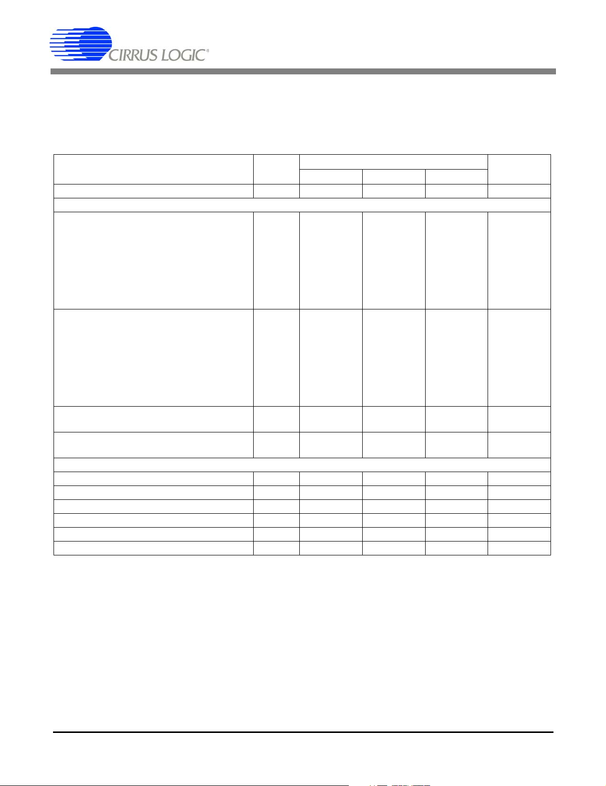
1. CHARACTERISTICS & SPECIFICATIONS
CS5371 CS5372
ANALOG CHARACTERISTICS Notes:T
= -40 C to +85 C; VA+ = 5V or 2.5V ± 5%; VA - = 0V or
A
-2.5V ± 5%; VD = 5V or 3.3V ± 5%; DGND = 0V; MCLK = 2.048 MHz; [(VREF+) - (VREF-)] = 2.5V;
Devices are connected as shown in Figure 3, the System Connection Diagram.
CS5371-BS / CS5372-BS
Parameter Symbol
Specified Temperature Range T
A
-40 - +85 C
UnitMin Typ Max
Dynamic Performance
Dynamic Range (Note 1)
LPWR = 0 0 Hz to 1720 Hz
MCLK = 2.048 MHz 0 Hz to 860 Hz
0 Hz to 430 Hz
0 Hz to 215 Hz
0 Hz to 107.5 Hz
0 Hz to 53.75 Hz
0 Hz to 26.875 Hz
Dynamic Range (Note 1)
LPWR = 1 0 Hz to 1720 Hz
MCLK = 1.024 MHz 0 Hz to 860 Hz
0 Hz to 430 Hz
0 Hz to 215 Hz
0 Hz to 107.5 Hz
0 Hz to 53.75 Hz
0 Hz to 26.875 Hz
Total Harmonic Distortion (Note 2)
SNR
-
-
-
-
-
-
-
-
-
-
-
-
-
-
SNR
LP
-
-
121
-
-
-
-
-
-
118
-
-
-
-
109
121
124
127
130
133
136
106
118
121
124
127
130
133
THD - -118 -112 dB
dB
dB
dB
dB
dB
dB
dB
dB
dB
dB
dB
dB
dB
dB
LPWR = 0; MCLK = 2.048 MHz
Total Harmonic Distortion (Note 2)
THD
LP
--114-108dB
LPWR = 1; MCLK = 1.024 MHz
DC Accuracy
Channel to Channel Gain Variation (Note 3) CGV - 1 - %
Full-scale Drift (Notes 3 and 4) TC
Offset (Note 3) V
FS
ZSE
-5-ppm/C
-1-mV
Offset after Calibration (Note 5) - ±1 - µV
Offset Calibration Range (Note 6) - 100 - %F.S.
Offset Drift (Notes 3 and 4) TC
ZSE
-1-µV/C
Notes: 1. Dynamic Range defined as 20 log [ (RMS full scale) / (RMS idle noise) ]
2. Tested with full-scale input signal of 31.25 Hz; OWR = 1000 SPS; OFST = 1.
3. Specification is for the parameter over the specified temperature range for the CS5371/72 devices only
and does not include the effects of external components.
4. Specifications are guaranteed by design and/or characterization.
5. The offset after calibration specification applies to the effective offset voltage for a full-scale input to the
CS5371/72 modulator, but is measured from the output digital codes from the digital filter.
6. The CS5371/72 offset calibration is performed digitally and includes the full-scale range.
DS255F3 3
CS5371 CS5372
ANALOG CHARACTERISTICS (Continued)
Parameter Symbol Min Typ Max Unit
Specified Temperature Range T
Input Characteristics
Input Signal Frequencies (Note 7) BW DC - 1720 Hz
Input Voltage Range (Note 8) VIN - - 5 V
Input Over-range Voltage Tolerance (Note 8) I
Input Signal plus Common Mode (VA-)
Common Mode Rejection Ratio CMRR - 90 - dB
Channel Crosstalk (CS5372 only) CXT - -120 - dB
Voltage Reference Input
VREF (VREF+) - (VREF-) - 2.5 - V
VREF Current - - 120 µA
Power Supplies
DC Power Supply Currents (Note 9 and 10)
LPWR = 0; MCLK = 2.048 MHz Analog
Digital
LPWR = 1; MCLK = 1.024 MHz Analog
Digital
Power Down Modes
CS5371 PWDN = 1
PWDN = 1, MCLK = 0
A
OVR
VA
VD
VA
VD
P
D
-40 - +85 C
5--%F.S.
-(VA+)
+ 0.7V
-
-
-
-
-
-
5.0
0.2
3.0
0.2
1
10
- 1.7V
7.0
0.3
4.5
0.3
-
-
mA
mA
mA
mA
mW
µW
p-p
V
CS5372 PWDN1 or PWDN2 = 1
PWDN1 = PWDN2 = 1
PWDN1 = PWDN2 = 1, MCLK = 0
Power Supply Rejection (Note 11) PSRR - 90 - dB
Notes: 7. The upper bandwidth limit is determined by the digital filter. A simple single pole anti-alias filter with a -
3 dB frequency at (MCLK / 256) should be placed in front of each channel.
8. The input voltage range is for the configuration depicted in Figure 3, the System Connection Diagram,
and applies to signal frequencies from DC to the stop-band frequency selected in the digital filter.
9. Per channel. All outputs unloaded. All digital inputs forced to VD or GND respectively.
10. In Low Power Mode LPWR = 1, the Master Clock MCLK is reduced to 1.024 MHz. This reduces the
oversampled signal bandwidth by a factor of 2.
11. Tested with a 50 Hz 100 mVpp sine wave applied separately to each supply.
-
-
-
25
1
10
-
-
-
mW
mW
µW
4 DS255F3
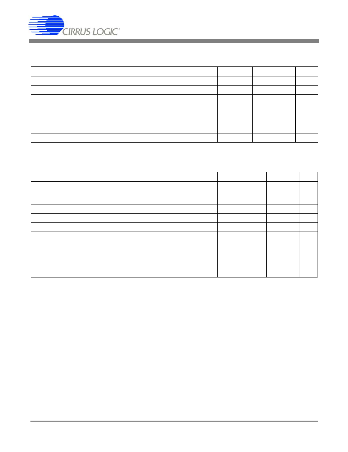
CS5371 CS5372
DIGITAL CHARACTERISTICS Notes:T
= 25 C; VA+ = 5V or 2.5V ±5%; VA- = 0V or -2.5V ±5%;
A
VD = 5V or 3.3V ± 5%; DGND = 0V; All voltages with respect to DGND.
Parameter Symbol Min Typ Max Unit
High-level Input Voltage V
Low-level Input Voltage V
High-level Output Voltage I
Low-level Output Voltage I
= -5.0 mA V
out
= 5.0 mA V
out
Input Leakage Current I
3-state Leakage Current I
Digital Output Pin Capacitance C
IH
IL
OH
OL
in
OZ
out
0.6 * VD - VD V
0.0 - 0.8 V
(VD) - 1.0 - - V
--0.4V
-±1±10µA
--±10µA
-9-pF
ABSOLUTE MAXIMUM RATINGS Notes:DGND = 0 V
Parameter Symbol Min Typ Max Unit
DC Power Supplies (Notes 12 and 13) Positive Digital
Positive Analog
Negative Analog
Input Current, Any Pin Except Supplies (Note 14 and 15) I
Input Current, Supplies (Note 15) I
Output Current I
Power Dissipation (Note 16) PDN - - 500 mW
Analog Input Voltage All Analog Pins V
Digital Input Voltage All Digital Pins V
Ambient Operating Temperature T
Storage Temperature T
VD
VA+
VA-
IN
IN
OUT
INA
IND
A
stg
-0.3
-0.3
-3.3
-
-
-
+6.0
+6.0
+0.3
--±10mA
--±50mA
--±25mA
(VA-) - 0.5 - (VA+) + 0.5 V
-0.5 - (VD) + 0.5 V
-40 - 85 °C
-65 - 150 °C
V
V
V
Notes: 12. VA+ and VA- must satisfy {(VA+) - (VA-)} < +6.8 V.
13. VD and VA- must satisfy {(VD) - (VA-)} < +7.6 V.
14. Includes continuous over-voltage conditions at the analog input (AIN) pins.
15. Transient current of up to 100 mA can be safely tolerated without SCR latch-up.
16. Total power dissipation, including all input and output currents.
DS255F3 5
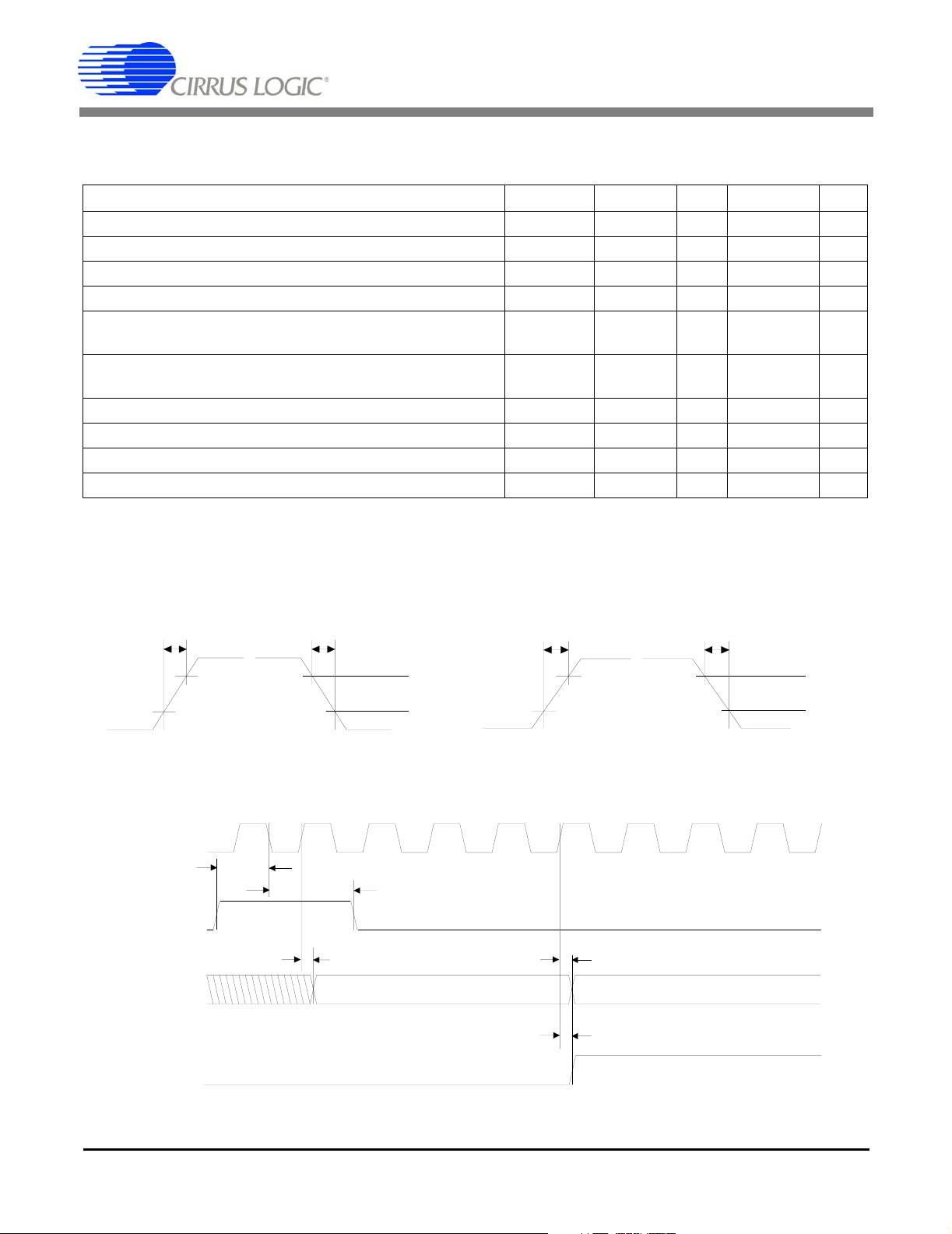
CS5371 CS5372
SWITCHING CHARACTERISTICS Notes:T
= 0V or -2.5V ± 5%; VD = +5V or +3.3V ± 5%; Digital Inputs: Logic 0 = 0V, Logic 1 = VD; C
= -40 C to +85 C; VA+ = +5V or +2.5V ± 5%; VA-
A
=50pF
L
Parameter Symbol Min Typ Max Unit
MCLK Frequency (Note 17) f
c
0.1 2.048 2.2 MHz
MCLK Duty Cycle 40 - 60 %
MCLK Jitter (In-band or aliased in-band) - - 300 ps
MCLK Jitter (Out-of-band) - - 1 ns
Rise Times: Any Digital Input (Note 18)
Any Digital Output
Fall Times: Any Digital Input (Note 18)
Any Digital Output
MSYNC Setup Time to MCLK falling (Note 19) t
MSYNC Hold Time after MCLK falling t
MCLK rising to Valid MFLAG t
MCLK rising to Valid MDATA t
t
risein
t
riseout
t
fallin
t
fallout
mss
msh
mfh
mdv
-
-
-
-
50
50
-
50
100
-
50
100
20 - - ns
20 - - ns
-3565ns
-6090ns
Notes: 17. If MCLK is removed, the CS5372 enters a micro power state.
18. Excludes MCLK input, MCLK should be driven with a signal having rise/fall times of 25 ns or faster.
19. MSYNC latched on MCLK falling edge, data output on next MCLK rising edge.
ns
ns
ns
ns
MCLK
t
mss
MSYNC
MDATA
MFLAG
t
risein
t
t
fallin
mdv
0.9 * VD
0.1 * VD
Figure 1. Rise and Fall Times
t
msh
VALID DATA
t
riseout
t
mdv
t
mfh
VALID DATA
t
fallout
0.9 * VD
0.1 * VD
Figure 2. CS5372 Interface Timing
6 DS255F3

CS5371 CS5372
2. GENERAL DESCRIPTION.
The CS5371 and CS5372 are one- and two- channel fourth-order ∆Σ modulators, optimized for extremely high-resolution measurement of signals
between DC and 1600 Hz. They are designed to
be used with the CS5376A and CS5378 low-power
digital filters. Figure 3 on page 8 shows a fourchannel system connection diagram for two
CS5372 and one CS5376A.
High Performance
The CS5371/72 modulators have exceptional performance characteristics. Modulator dynamic
range (SNR) is 127 dB over a 215 Hz bandwidth
(2 ms sampling), with total harmonic distortion
(THD) of -118 dB.
Low Power Consumption
The CS5371/72 modulators have very low power
consumption. Power consumption is only 25 mW
per channel in normal mode (LPWR=0,
MCLK=2.048 MHz), and 15 mW per channel in low
power mode (LPWR=1, MCLK=1.024 MHz).
An independently selectable power-down mode
(PWDN=1) can be used to disable a modulator and
reduces its power consumption to 1 mW. If MCLK
is then halted (MCLK=0), the modulator enters a
micropower state using only 10
µW per channel.
Small Package Size
The CS5371/72 modulators are available in a very
small 24-pin SSOP package approximately
8 mm x 8 mm in size. The CS5372 has two modulator channels per package to increase board layout density even further.
Multi-channel System Support
Combining the CS5371 and CS5372 modulators
with a digital filter permits multiple system configurations:
1 Channel - CS5371, CS5378
2 Channel - CS5372, CS5376A
3 Channel - CS5371, CS5372, CS5376A
4 Channel - CS5372, CS5372, CS5376A
Differential Analog Signal Inputs
The CS5371/72 modulators have fully differential
analog inputs capable of measuring signals up to
5.0 V peak-to-peak when using a 2.5 V voltage reference. The inputs will tolerate a 5% over-range
voltage and continue operating at full specification.
Digital Filter Interface
The CS5371/72 modulators are designed to operate with the CS5376A and CS5378 digital filters.
The digital filter generates the modulator clock and
synchronization signal inputs (MCLK and
MSYNC), while receiving the modulator data and
over-range flag outputs (MDATA and MFLAG).
The modulators produce an oversampled ∆Σ serial
bit stream at 512 kbits per second when operated
from a 2.048 MHz modulator clock.
Multiple Power Supply Configurations
The CS5371/72 modulators support flexible power
supply configurations. They can run from single or
dual supplies in the following configurations:
VA+ = +5V; VA- = 0V; VD = +3.3V to +5V
VA+ = +2.5V; VA- = -2.5V; VD = +3.3V
DS255F3 7
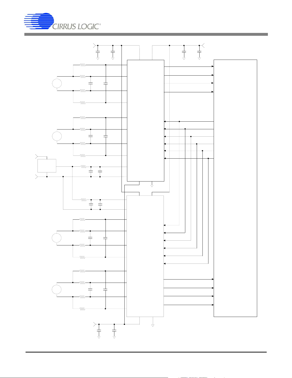
CS5371 CS5372
VA +
VA -
Channel 1
VREF
VA+
100 µF
499 Ω
499 Ω
~
499 Ω
499 Ω
499 Ω
499 Ω
~Channel 2
499 Ω
499 Ω
10 Ω
100 µF
0.02 µF
COG
0.02 µF
COG
0.01 µF
0.02 µF
0.02 µF
0.01µF
X7R
X7R
INRI+
INFI+
INFI-
INRI-
INR2+
INF2+
INF2-
INR2-
VREF+
VREF-
VA+ VD
M
F
MDATA1
MFLAG2
MDATA2
CS5372
MSYNC
PWDN1
PWDN2
VA- DGND
0.01 µF
LAG1
MCLK
OFST
LPWR
VD
100 µF
MFLAG1
MDATA1
MFLAG2
MDATA2
MCLK
MSYNC
GPIO4
GPIO5
GPIO6
GPIO7
CS5376A
10 Ω
100 µF
499 Ω
499 Ω
~Channel 3
499 Ω
499 Ω
499 Ω
499 Ω
~Channel 4
499 Ω
499 Ω
VA -
100 µF
0.02 µF
COG
0.02 µF
COG
0.01µF
0.01 µF
0.02 µF
X7R
0.02 µF
X7R
VREF+
VREF-
INRI+
INFI+
INFI-
INRI-
INR2+
INF2+
INF2-
INR2-
VA+ VD
MSYNC
PWDN1
PWDN2
CS5372
MFLAG1
MDATA1
MFLAG2
MDATA2
VA- DGND
MCLK
OFST
LPWR
MFLAG3
MDATA3
MFLAG4
MDATA4
Figure 3. System Connection Diagram
8 DS255F3
CS5371 CS5372
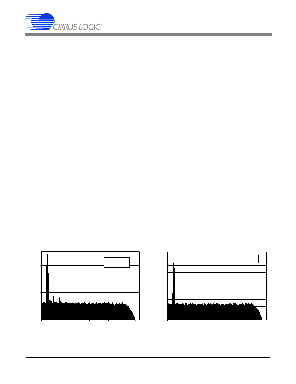
3. MODULATOR PERFORMANCE
Figures 4 and 5 illustrate the spectral performance
of the CS5371/72 modulators when combined with
the CS5376A or CS5378 digital filter. The plots
were created from ten averaged 1024 point FFTs.
3.1. Full-scale Signal Performance
Figure 4 illustrates the full-scale signal performance of the CS5371/72 modulators and digital filter using a 31.25 Hz input signal and a 1000 SPS
output word rate. The outstanding full-scale signal
characteristics of the CS5371/72 modulators are
shown, with no harmonic components exceeding 120 dB. Analysis of this data set yields a signal-tonoise ratio (SNR) of 124.0 dB and a signal-to-distortion ratio (SDR) of 119.0 dB. Note that the fullscale signal peak in Figure 4 shows a slightly reduced amplitude due to spectral smearing associated with the FFT windowing function, and is a
purely digital phenomenon.
3.2. Noise Performance
Figure 5 illustrates the noise performance of the
CS5371/72 modulators and digital filter using a
31.25 Hz -24 dB input signal at a 1000 SPS output
word rate. The outstanding noise characteristics of
the CS5371/72 modulators are shown, with the averaged noise components consistently below the
-150 dB level. Analysis of this data set yields a dynamic range of 124.7 dB. Note that the 0.7 dB
variation between the signal-to-noise calculation in
Figure 4 and the dynamic range calculation in Figure 5 is not modulator dependent and results from
jitter in the test signal generator when producing a
full-scale output, as evidenced by the skirt surrounding the signal peak below the -140 dB level in
Figure 4.
4. SIGNAL INPUTS
The CS5371/72 modulators use a switched capacitor architecture for the analog signal inputs, which
has increased jitter tolerance compared with continuous time signal input stages.
4.1. Differential Inputs - INR+/-, INF+/-
The analog signal inputs are differential and use
four pins: INR+, INR-, INF+, and INF-. Two inputs,
INR+ and INF+, are connected to the positive half
of the differential signal, while two inputs, INR- and
INF-, are connected to the negative half. The INR+
and INR- pins are switched capacitor ‘rough
charge’ inputs that pre-charge the internal sampling capacitor before it is connected to the INF+
and INF- fine input pins.
The full-scale analog signal span is defined by the
voltage applied across the VREF+ and VREFpins. A 2.5 volt reference input sets full-scale signals as 5 volts peak-to-peak, fully differential. Differential inputs increase the dynamic range of
0
-20
-40
-60
-80
-100
dB
-120
-140
-160
-180
-200
0 50 100 150 200 250 300 350 400 450 500
Figure 4. 1024 Point FFT plot with a 31.25 Hz
input at Full-scale, ten averages
Hz
S/N = 124.0 dB
S/D = 119.0 dB
0
-20
-40
-60
-80
-100
dB
-120
-140
-160
-180
-200
0 50 100 150 200 250 300 350 400 450 500
Figure 5. 1024 Point FFT plot with a 31.25 Hz
input at -24 dB, ten averages
Dynamic Range = 124.7 dB
Hz
DS255F3 9

CS5371 CS5372
small signals, reducing the gain requirements for
input amplifier stages by a factor of two relative to
single ended analog inputs.
4.2. Anti-alias Filters
The CS5371/72 modulator inputs must be bandwidth limited to ensure modulator loop stability and
to prevent aliased high-frequency signals. The
modulators are 4th order and so are conditionally
stable, and can be adversely affected by high amplitude out-of-band signals. Also, aliasing effects
degrade modulator performance if the analog inputs are not bandwidth limited since out-of-band
signals can appear in the measurement bandwidth. The use of a simple single pole low-pass
anti-alias filter on the differential inputs ensures
out-of-band signals are eliminated.
Anti-alias filtering may be accomplished actively in
an amplifier stage ahead of the CS5371/72 modulator, or passively using an RC filter across the differential rough and fine analog inputs. An RC filter
is recommended, even when using an amplifier
stage, as it minimizes the ‘charge kick’ that the
driving amplifier sees as switched capacitor sampling is performed.
The -3 dB corner of the input anti-alias filter should
be set to the internal modulator sampling clock divided by 64. The modulator sampling clock is a division by 4 of the modulator clock, MCLK. With
MCLK=2.048 MHz the modulator sampling clock is
512 kHz, requiring an input filter with a -3 dB corner at 8 kHz.
MCLK Frequency = 2.048 MHz
Sampling Frequency = MCLK / 4 = 512 kHz
-3 dB Filter Corner = Sample Freq / 64 = 8 kHz
RC filter = 8 kHz = 1 / [ 2π * (2 * R
It should be noted that when using low power
mode (LPWR=1 and MCLK=1.024 MHz) the modulator sampling clock is 256 kHz, so the -3 dB filter
corner should be scaled down to 4 kHz.
MCLK Frequency = 1.024 MHz
Sampling Frequency = MCLK / 4 = 256 kHz
diff
) * C
diff
]
Figure 3 illustrates the CS5372/CS5376A system
connections with input anti-alias filter components.
Filter components on the rough and fine pins
should be identical values for optimum performance, with the capacitor values a minimum of
0.02 µF. The rough input can use either X7R or
C0G capacitors, while the fine input requires C0G
type capacitors for optimal linearity. Using X7R capacitors on the fine inputs will degrade signal to
distortion performance up to 8 dB.
4.3. Input Impedance
Due to the dynamic switched-capacitor input architecture, the input current required from the analog
signal source and thus the input impedance of the
analog input pins changes any time MCLK is
changed. The input impedance of the rough
charge inputs, INR+ and INR-, is [1 / (f * C)] where
f is the modulator clock frequency, MCLK, and C is
the internal sampling capacitor. A 2.048 MHz
modulator clock yields a rough input impedance of
approximately [1 / (2.048 MHz)*(20 pF)], or about
24 kΩ.
Internal to the modulator the rough charge inputs
pre-charge the sampling capacitor used by the fine
inputs, therefore the input current to the fine inputs
is very low and the effective input impedance is orders of magnitude above the impedance of the
rough inputs.
4.4. Maximum Signal Levels
The CS5371/72 modulators are 4th order and are
therefore conditionally stable, and may go into an
oscillatory condition if the analog inputs over-range
beyond full scale by more than 5%. If an unstable
condition is detected, the modulators collapse to a
1st order system until loop stability is achieved.
During this time, the MFLAG pin transitions from
low to high signaling the digital filter to set an error
bit in the digital output status word. The analog input signal must be reduced to within the full-scale
range of the converter for at least 32 MCLK cycles
for the modulators to recover from an unstable
condition.
-3 dB Filter Corner = Sample Freq / 64 = 4 kHz
RC filter = 4 kHz = 1 / [ 2π * (2 * R
10 DS255F3
diff
) * C
diff
]
5. INPUT OFFSET
The CS5371/72 modulators are ∆Σ type and so
can produce ‘idle tones’ in the passband when the

CS5371 CS5372
input signal is a steady state DC signal within
±50 mV of the common mode input voltage. Idle
tones result from patterns in the output bitstream
and appear in the measurement spectrum about
-135 dB down from full scale.
Idle tones can be eliminated by adding differential
DC offset to the modulator inputs. The added offset should be applied differentially to the inputs,
common mode offsets do not affect idle tones.
5.1. Offset Enable - OFST
If the analog inputs are near the common mode
voltage when no signal is present, the OFST pin
can be used to eliminate idle tones. When
OFST=1, -50 mV of differential offset is added to
the modulator analog inputs to push the idle tones
out of the measurement bandwidth. Care should
be taken that when OFST is active, offset voltages
generated by external circuitry do not negate the
internally added offset.
5.2. Offset Drift
Offset drift characteristics vary from part to part
and with changes in the power supply voltages. If
the CS5371/72 is used in precision DC measurement applications where offset drift is to be minimized, the power supplies should be well
regulated.
For the lowest offset drift, the CS5371/72 modulators should operate with an MCLK of 2.048 MHz.
The offset drift rate is inversely proportional to
clock frequency, with slower modulator clock rates
exhibiting more offset drift. Operating from an
MCLK of 1.024 MHz results in twice the offset drift
rate compared to an MCLK of 2.048 MHz.
Because offset drift is not linear with temperature,
an exact drift rate per °C cannot be specified. The
CS5371/72 modulators will exhibit approximately
5 ppm/°C of offset drift operating with an MCLK of
2.048 MHz.
6. VOLTAGE REFERENCE INPUTS
The CS5371/72 modulators are designed to operate with a 2.5 V voltage reference applied across
the VREF+ and VREF- pins to set the full-scale signal range of the analog inputs. A 2.5 V voltage reference results in the highest dynamic range and
best signal-to-noise performance, though smaller
reference voltages may be used. When the
CS5371/72 modulators are operated with a 2.5 V
reference, the analog inputs measure full-scale
signals of 5 volts peak-to-peak fully differential.
In a single supply power configuration the voltage
reference output should be connected to the
VREF+ pin with the VREF- pin connected to
ground. In a dual supply power configuration the
voltage reference should be powered from the VA+
and VA- supplies, with the modulator VREF+ pin
connected to the voltage reference output and the
VREF- pin connected to VA-. Because most 2.5 V
voltage references require a power supply voltage
greater than 3 V to operate, when powering the
voltage reference from dual supplies the reference
voltage into the VREF+ pin should be defined relative to the VA- supply.
The selected voltage reference should produce
less than 1 µVrms of noise in the measurement
bandwidth on the VREF+ pin. The digital filter output word rate selection determines the bandwidth
DS255F3 11

CS5371 CS5372
over which voltage reference noise affects the
CS5371/72 modulator dynamic range.
6.1. Voltage Reference Configurations
For a 2.5 V reference, the Linear Technology
LT1019-2.5 voltage reference yields low enough
noise if the output is filtered with a low pass RC filter as shown in Figure 6. The filtered version in
Figure 6 is acceptable for most spectral measurement applications, but a buffered version with lower source impedance may be preferred for DC
measurement applications.
6.2. VREF Input Impedance
The switched-capacitor input architecture of the
VREF+ pin causes the input current required from
the voltage reference to change any time MCLK is
changed. The input impedance of the voltage reference input is calculated similar to the analog signal input impedance as [1 / (f * C)] where f is the
modulator clock frequency, MCLK, and C is the internal sampling capacitor. A 2.048 MHz MCLK
yields a voltage reference input impedance of approximately [1 / (2.048 MHz)*(20 pF)], or about
24 kΩ.
6.3. Gain Accuracy
Gain accuracy of the CS5371/72 modulators is affected by variations of the voltage reference input.
A change in the voltage reference input impedance
due to a change in MCLK could affect gain accura-
cy when using the higher source impedance configuration of Figure 6. The VREF+ pin input
impedance and the external low-pass filter resistor
create a voltage divider for the output reference
voltage, reducing the effective voltage reference
input. If gain error is to be minimized, especially
when MCLK is to be changed, the voltage reference should have a low output impedance to minimize the effect of the resistive voltage divider. A
buffered voltage reference configuration offers
lower output impedance and more stable gain
characteristics.
6.4. Gain Drift
Gain drift of the CS5371/72 modulators due to temperature is around 5 ppm/°C, and does not include
the temperature drift characteristics of the external
voltage reference. Gain drift is not affected by the
modulator sample rate or by power supply variations.
7. DIGITAL FILTER INTERFACE
The CS5371/72 modulators are designed to operate with the CS5376A and CS5378 digital filters.
The digital filter generates the modulator clock and
synchronization signal inputs (MCLK and
MSYNC), while receiving the modulator data and
over-range flag outputs (MDATA and MFLAG).
The modulators produce an oversampled ∆Σ serial
+VA
-VA
12 DS255F3
10
10
µ
F
0.1µF
Ω
10
2.5 REF
0.1µF 100µF
µ
F
0.1µF
Figure 6. 2.5 Voltage Reference
+
To VREF+
To VREF -

CS5371 CS5372
bit stream at 512 kbits per second when operated
from a 2.048 MHz modulator clock.
7.1. Modulator Clock - MCLK
For proper operation, the CS5371/72 modulators
must be provided with a CMOS compatible clock
on the MCLK pin. MCLK is internally divided by
four to generate the modulator sampling clock.
MCLK must have less than 300 ps of in-band jitter
to maintain full performance specifications.
When used with the CS5376A or CS5378 digital filter, MCLK is automatically generated and is typically 2.048 MHz or 1.024 MHz. MCLK can be
generated by other means, using a crystal oscillator for example, and can run any rate between
100 kHz and 2.2 MHz. If MCLK is disabled, the
modulators are automatically placed into a micropower state. They are equipped with loss of clock
detection circuitry to force power down if MCLK is
removed.
The choice of MCLK frequency affects the performance of the CS5371/72 modulators. They exhibit
the best dynamic range (SNR) performance with
faster MCLK rates because of increased oversampling of the analog input signal. The modulators
exhibit the best total harmonic distortion (THD)
performance with slower MCLK rates because
slower sampling allows more time to settle the analog input signal.
7.2. Modulator Data - MDATA
The CS5371/72 modulators output a ∆Σ serial bitstream to the MDATA pin, with a one’s density proportional to the amplitude of the analog input signal
and a bit rate determined by the modulator sampling clock. The modulator sampling clock is a divide by four of MCLK, so for a 2.048 MHz MCLK
the modulator sampling clock and MDATA output
bit rate will be 512 kHz.
The MDATA output has a one’s density defined as
nominal 50% for no signal input, 86% for positive
full scale, and 14% for negative full scale. It has a
maximum positive over-range capability to 93%
and a maximum negative over-range capability to
7%. The one’s density of the MDATA output is defined as the ratio of ‘1’ bits to total bits in the serial
bitstream output, i.e. an 86% one’s density has, on
average, a ‘1’ value in 86 of every 100 output data
bits.
When operated with the CS5376A or CS5378 digital filter, the full-scale 24-bit output codes range
from 0x5D1C41 to 0xA2EAAE with the internal
OFST disabled.
Digital Filter
Modulator Input
Signal
> + (VREF + 5%) Error Flag Possible
+VREF 5D1C41 5B3A71
0V 000000 FE21D8
-VREF A2EAAE A108DE
> - (VREF + 5%) Error Flag Possible
Table 1. Output coding for the CS5371/72 and digital
filter combination
Note that for a full-scale input signal, 5 V
Output Code
OFST=0 OFST=1
pp
with
VREF=2.5 V, the CS5371/72 and CS5376A/78
chipset does not output a maximum 24-bit 2’s complement digital code of 0x7FFFFF, but instead a
lower scaled value to allow over-range capability.
7.3. Modulator Sync - MSYNC
To synchronize the analog sampling instant and
timing of the digital output bitstream, the
CS5371/72 modulators use an MSYNC signal.
When using the CS5376A or CS5378 digital filter,
MSYNC is automatically generated from a SYNC
signal input from the external system.
The MSYNC input is rising edge triggered and resets the internal MCLK counter-divider so the analog sampling instant occurs during a consistent
MCLK phase. It also sets the MDATA output timing so the bitstream can be properly sampled by
the digital filter input.
7.4. Modulator Flag - MFLAG
The CS5371/72 modulators are 4th order ∆Σ and
are therefore conditionally stable. The modulators
may go into an oscillatory condition if the analog inputs are over-ranged more than 5% past either
positive or negative fullscale.
If an unstable condition is detected, the modulators
collapse to a 1st order system until loop stability is
DS255F3 13

CS5371 CS5372
achieved. During this time, the MFLAG pin transitions from low to high to signal an error condition.
The analog input signal must be reduced to within
the full-scale range for at least 32 MCLK cycles for
the modulator to recover from an unstable condition.
The MFLAG output connects to a dedicated input
on the digital filter, causing an error bit to be set in
the status portion of the digital output data word
when detected.
8. POWER MODES
Four power modes are available when using the
CS5371/72 modulators. Normal power and low
power modes are operational modes, power down
and micro-power modes are non-operational
standby modes.
8.1. Normal Power Mode
The normal operational mode for the modulators,
LPWR=0 and MCLK=2.048 MHz, provides the
best performance with power consumption of
25 mW per channel. This power mode is recommended when maximum conversion accuracy is
required.
8.2. Low Power Mode - LPWR
The modulators have a low-power operational
mode, LPWR=1 and MCLK=1.024 MHz, that reduces power consumption to 15 mW per channel
at the expense of 3 dB of dynamic range. This operational mode is recommended when minimizing
power is more important than maximizing dynamic
range.
When operated with LPWR=1, the modulator sampling clock (MCLK / 4) must be restricted to rates
of 256 kHz or less, which requires MCLK to run at
1.024 MHz or less. Operating in low power mode
with modulator sample rates greater than 256 kHz
will significantly degrade total harmonic distortion
performance.
PWDN on the CS5371 and PWDN1, PWDN2 on
the CS5372. Note that when the modulators are
powered down and MCLK is active, the internal
clock generator is still drawing minimal currents.
8.4. Micro-power Mode
Standby power consumption of the modulators can
be minimized by placing them into a micro-power
mode, PWDN=1 and MCLK=0. Micro-power mode
requires setting the PWDN pin and halting MCLK
to remove the clock generator input current. Micropower mode consumes only 10 µW of power.
9. POWER SUPPLY
The CS5371/72 modulators have one positive analog power supply pin, VA+, one negative analog
power supply pin, VA-, one digital power supply
pin, VD, and one digital ground pin, DGND. The
analog and digital circuitry is separated internally
to enhance performance, therefore power must be
supplied to all three supply pins and the digital
ground pin must be connected to system ground.
9.1. Power Supply Configurations
The CS5371/72 analog supplies can be powered
by a single +5 V supply and analog ground, or by
dual supplies of ± 2.5 V. When using dual supplies, the positive and negative analog power supplies must satisfy the following conditions:
(VA+) - (VA-) < 6.8 volts
(VD) - (VA-) < 7.6 volts
These conditions permit several power supply configurations.
VA+ = +5V; VA- = 0V; VD+ = +3.3V to +5V
VA+ = +2.5V;VA- = -2.5V; VD+ = +3.3V
When used with the CS5376A or CS5378 digital filter the maximum voltage differential between the
modulator digital supply, VD, and the CS5376A/78
I/O supply, VDD2 or VDDPAD, must be 0.3V or
less.
8.3. Power Down Mode - PWDN
The modulators have a power down mode,
PWDN=1 and MCLK=Active, that disables the operation of the selected modulator channel and reduces its power consumption to 1 mW. Each
modulator has an independent power down pin,
14 DS255F3
9.2. Power Supply Bypassing
The analog and digital supply pins, VA+, VA-, and
VD, should be decoupled to system ground with
0.01 µF and 10 µF capacitors, or with a single
0.1 µF capacitor. Bypass capacitors can be X7R,
tantalum, or any other dielectric types.

CS5371 CS5372
9.3. SCR Latch-up Considerations
The VA- pin is tied to the CS5371/72 substrate and
should always be connected to the most negative
supply voltage to ensure SCR latch-up does not
occur. In general, latch-up may occur when any
pin voltage (including the analog inputs) is 0.7V or
more below VA-, or 7.6V or more above VA-.
Analog inputs INR+/- and INF+/- should be voltage
limited to ensure signals don’t exceed the (VA-)-
0.7V or (VA+)+7.6V requirement. Either the inputs
should be clamped to the VA+ and VA- rails using
reversed biased Schottky diodes (BAT85 or similar), or the current into the analog inputs should be
limited to less than 10mA. By current limiting the
analog inputs, the internal ESD diodes on the analog input pads will clamp the input signal to the
proper level. Input currents greater than 10mA will
overdrive the internal diodes, so external components are required.
When using dual analog power supplies, it is recommended to connect the VA- power supply pin to
system ground (DGND) using a reversed biased
Schottky diode. This configuration clamps the VA-
voltage a maximum of 0.3V above ground to ensure SCR latch-up does not occur during power
up. If the VA+ power supply ramps before the VAsupply, the VA- voltage could be pulled above
ground through the CS5371/72. If the VA- supply
is unintentionally pulled 0.7 V above the DGND
pin, SCR latch-up can occur.
9.4. DC-DC Converter Considerations
Many measurement systems are battery powered
and utilize DC-DC converters to generate the necessary supply voltages for the system. To minimize the effects of interference, it is desirable to
operate the DC-DC converter at a frequency which
is rejected by the digital filter.
9.5. Power Supply Rejection
Power supply rejection of the CS5371/72 modulators is frequency dependent. The digital filter rejects power supply noise for frequencies above the
filter corner frequency at 130 dB or greater. For
frequencies between DC and the digital filter corner frequency, power supply rejection is nearly
constant at 90 dB.
DS255F3 15

10. PIN DESCRIPTION - CS5371
CS5371 CS5372
Rough Non-Inverting Input INR+
Fine Non-Inverting Input INF+
Fine Inverting Input INF-
Rough Inverting Input INR-
Positive Voltage Reference Input VREF+
Negative Voltage Reference Input VREF-
Negative Analog Power Supply VA-
Positive Analog Power Supply VA +
No Internal Connection NC
No Internal Connection NC
No Internal Connection NC
No Internal Connection NC
Power Supplies
VA+ _ Positive Analog Power Supply, pin 8
Positive supply voltage.
1
2
3
4
5
6
7
817
9
10
11
12 13
PWDN Power-down Enable
24
LPWR Low Power Mode Select
23
MFLAG Modulator Flag Output
22
MDATA Modulator Data Output
21
MSYNC Modulator Sync Input
20
MCLK Modulator Clock Input
19
18
VD Positive Digital Power Supply
DGND Digital Ground
NC No Internal Connection
16
NC No Internal Connection
15
OFST Offset Mode Select
14
VD Positive Digital Power Supply
VA- _ Negative Analog Power Supply, pin 7
Negative supply voltage.
VD _ Positive Digital Power Supply, pin 13, 18
Positive supply voltage.
DGND _ Digital Ground, pin 17
Analog Inputs
INR+ _ Rough Non-Inverting Input, pin 1
Rough non-inverting analog input. The rough input settles non-linear currents to improve
linearity on the fine input and reduce harmonic distortion.
INR- _ Rough Inverting Input, pin 4
Rough inverting analog input. The rough input settles non-linear currents to improve linearity
on the fine input and reduce harmonic distortion.
INF+ _ Fine Non-Inverting Input, pin 2
Fine non-inverting analog input.
16 DS255F3
INF- _ Fine Inverting Input, pin 3
Fine inverting analog input.
VREF+ _ Positive Voltage Reference Input, pin 5
Input for an external +2.5 V voltage reference relative to VREF-.
VREF- _ Negative Voltage Reference Input, pin 6
This pin should be tied to VA-.
Digital Inputs
MCLK _ Modulator Clock Input, pin 19
A CMOS compatible clock input for the modulator internal master clock, nominally 2.048 MHz
with an amplitude equal to the VD digital power supply.
MSYNC _ Modulator Sync Input, pin 20
A low to high transition resets the internal clock phasing of the modulator. This assures the
sampling instant and modulator data output are synchronous to the external system.
CS5371 CS5372
OFST _ Offset Mode Select, pin 14
When high, adds approximately -50 mV of offset to the analog inputs to guarantee any ∆Σ idle
tones are removed. When low, no offset is added.
LPWR _ Low Power Mode Select, pin 23
When set high with MCLK operating at 1.024 MHz, modulator power dissipation is reduced to
15 mW per channel.
PWDN _ Power-down Mode, pin 24
When high, the modulator is in power-down mode and consumes 1 mW. Halting MCLK while
in power down mode reduces modulator power dissipation to 10
Digital Outputs
MDATA _ Modulator Data Output, pin 21
Modulator data is output as a 1-bit serial data stream at 512 kHz with an MCLK input of
2.048 MHz. Modulator data is output at 256 kHz with an MCLK input of 1.024 MHz.
MFLAG _ Modulator Flag Output, pin 22
A high level output indicates the modulator is unstable due to an over-range on the analog
inputs.
µW.
DS255F3 17
11. PIN DESCRIPTION - CS5372
CS5371 CS5372
Ch. 1 Rough Non-Inverting Input INR1+
Ch. 1 Fine Non-Inverting Input INF1+
Ch. 1 Fine Inverting Input INF1-
Ch. 1 Rough Inverting Input INR1-
Positive Voltage Reference Input VREF+
Negative Voltage Reference Input VREF-
Negative Analog Power Supply VA-
Positive Analog Power Supply VA +
Ch. 2 Rough Inverting Input INR2-
Ch. 2 Fine Inverting Input INF2-
Ch. 2 Fine Non-Inverting Input INF2+
Ch. 2 Rough Non-Inverting Input INR2+
Power Supplies
VA+ _ Positive Analog Power Supply, pin 8
Positive supply voltage.
1
2
3
4
5
6
7
817
9
10
11
12 13
PWDN1 Ch. 1 Power-down Enable
24
LPWR Low Power Mode Select
23
MFLAG1 Ch. 1 Modulator Flag Output
22
MDATA1 Ch. 1 Modulator Data Output
21
MSYNC Modulator Sync Input
20
MCLK Modulator Clock Input
19
18
VD Positive Digital Power Supply
DGND Digital Ground
MDATA2 Ch. 2 Modulator Data Output
16
MFLAG2 Ch. 2 Modulator Flag Output
15
OFST Offset Mode Select
14
PWDN2 Ch. 2 Power-down Enable
VA- _ Negative Analog Power Supply, pin 7
Negative supply voltage.
VD _ Positive Digital Power Supply, pin 18
Positive supply voltage.
DGND _ Digital Ground, pin 17
Analog Inputs
INR1+, INR2+ _ Channel 1 & 2 Rough Non-Inverting Inputs, pin 1, 12
Rough non-inverting analog inputs. The rough inputs settle non-linear currents to improve
linearity on the fine inputs and reduce harmonic distortion.
INR1-, INR2- _ Channel 1 & 2 Rough Inverting Inputs, pin 4, 9
Rough inverting analog inputs. The rough inputs settle non-linear currents to improve linearity
on the fine inputs and reduce harmonic distortion.
INF1+, INF2+ _ Channel 1 & 2 Fine Non-Inverting Input, pin 2, 11
Fine non-inverting analog inputs.
18 DS255F3

INF1-, INF2- _ Channel 1 & 2 Fine Inverting Input, pin 3, 10
Fine inverting analog inputs.
VREF+ _ Positive Voltage Reference Input, pin 5
Input for an external +2.5 V voltage reference relative to VREF-.
VREF- _ Negative Voltage Reference Input, pin 6
This pin should be tied to VA-.
Digital Inputs
MCLK _ Modulator Clock Input, pin 19
A CMOS compatible clock input for the modulator internal master clock, nominally 2.048 MHz
with an amplitude equal to the VD digital power supply.
MSYNC _ Modulator Sync Input, pin 20
A low to high transition resets the internal clock phasing of the modulator. This assures the
sampling instant and modulator data output are synchronous to the external system.
CS5371 CS5372
OFST _ Offset Mode Select, pin 14
When high, adds approximately -50 mV of offset to the analog inputs to guarantee any ∆Σ idle
tones are removed. When low, no offset is added.
LPWR _ Low Power Mode Select, pin 23
When set high with MCLK operating at 1.024 MHz, modulator power dissipation is reduced to
15 mW per channel.
PWDN1, PWDN2 _ Channel 1 & 2 Power-down Mode, pin 24, 13
When high, the modulator is in power down mode and consumes 1 mW. Halting MCLK while
in power down mode reduces modulator power dissipation to 10
Digital Outputs
MDATA1, MDATA2 _ Modulator Data Output, pin 21, 16
Modulator data is output as a 1-bit serial data stream at 512 kHz with an MCLK input of
2.048 MHz. Modulator data is output at 256 kHz with an MCLK input of 1.024 MHz.
MFLAG1, MFLAG2 _ Modulator Flag, pin 22, 15
A high level output indicates the modulator is unstable due to an over-range on the analog
inputs.
µW.
DS255F3 19
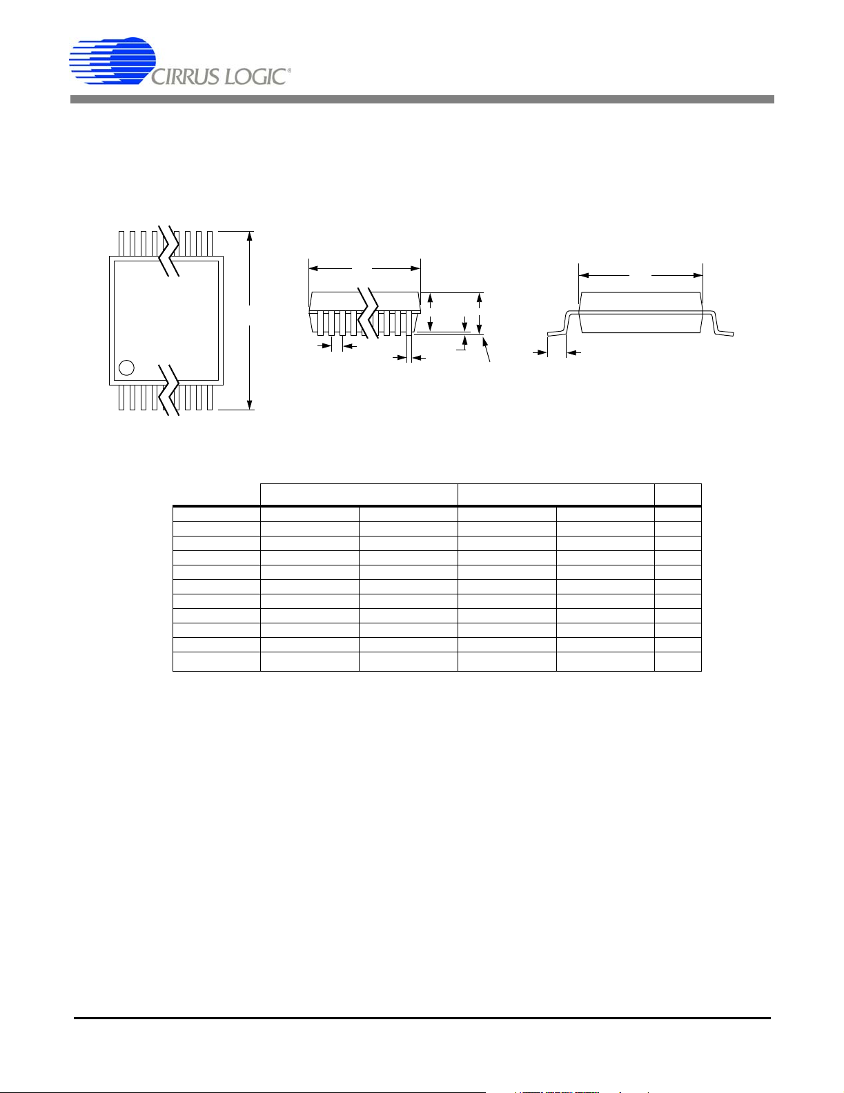
12.PACKAGE DIMENSIONS
24 PIN SSOP PACKAGE DRAWING
N
CS5371 CS5372
1
23
TOP VIEW
D
E
e
INCHES MILLIMETERS
DIM MIN MAX MIN MAX
A -- 0.084 -- 2.13
A1 0.002 0.010 0.05 0.25
A2 0.064 0.074 1.62 1.88
b 0.009 0.015 0.22 0.38 2,3
D 0.311 0.335 7.90 8.50 1
E 0.291 0.323 7.40 8.20
E1 0.197 0.220 5.00 5.60 1
e 0.024 0.027 0.61 0.69
L 0.025 0.040 0.63 1.03
∝
0° 8° 0° 8°
2
b
SIDE VIEW
A2
A1
A
SEATING
PLANE
L
1
E1
END VIEW
NOTE
Notes: 1. “D” and “E1” are reference datums and do not included mold flash or protrusions, but do include mold
mismatch and are measured at the parting line, mold flash or protrusions shall not exceed 0.20 mm per
side.
2. Dimension “b” does not include dambar protrusion/intrusion. Allowable dambar protrusion shall be
0.13 mm total in excess of “b” dimension at maximum material condition. Dambar intrusion shall not
reduce dimension “b” by more than 0.07 mm at least material condition.
3. These dimensions apply to the flat section of the lead between 0.10 and 0.25 mm from lead tips.
20 DS255F3
CS5371 CS5372
13.ORDERING INFORMATION
Model Temperature Package
CS5371-BS
CS5371-BSZ (lead free)
CS5372-BS
CS5372-BSZ (lead free)
14.ENVIRONMENTAL, MANUFACTURING, & HANDLING INFORMATION
Model Number Peak Reflow Temp MSL Rating* Max Floor Life
CS5371-BS
CS5371-BSZ (lead free)
CS5372-BS
CS5372-BSZ (lead free)
* MSL (Moisture Sensitivity Level) as specified by IPC/JEDEC J-STD-020.
-40 to +85 °C 24-pin SSOP
240 °C 2 365 Days
260 °C 3 7 Days
240 °C 2 365 Days
260 °C 3 7 Days
DS255F3 21
CS5371 CS5372
15.REVISION HISTORY
Revision Date Changes
PP2 AUG 2001 Preliminary release, updated with most-current characterization data.
F1 SEP 2005 Fix data sheet errata.
F2 SEP 2005 Corrected Table 1 on Page 13: When OFST=0 the 0V input is 0x000000, when
OFST=1 the 0V input is 0xFE21D8.
F3 OCT 2005 Corrected typical and maximum low-power THD on Page 3.
Corrected maximum input signal frequency on Page 4.
Contacting Cirrus Logic Support
For all product questions and inquiries contact a Cirrus Logic Sales Representative.
To find the one nearest to you go to www.cirrus.com
IMPORTANT NOTICE
Cirrus Logic, Inc. and its subsidiaries (“Cirrus”) believe that the information contained in this document is accurate and reliable. However, the information is subject
to change without notice and is provided “AS IS” without warranty of any kind (express or implied). Customers are advised to obtain the latest version of relevant
information to verify, before placing orders, that information being relied on is current and complete. All products are sold subject to the terms and conditions of sale
supplied at the time of order acknowledgment, including those pertaining to warranty, indemnification, and limitation of liability. No responsibility is assumed by Cirrus
for the use of this information, including use of this information as the basis for manufacture or sale of any items, or for infringement of patents or other rights of third
parties. This document is the property of Cirrus and by furnishing this information, Cirrus grants no license, express or implied under any patents, mask work rights,
copyrights, trademarks, trade secrets or other intellectual property rights. Cirrus owns the copyrights associated with the information contained herein and gives consent for copies to be made of the information only for use within your organization with respect to Cirrus integrated circuits or other products of Cirrus. This consent
does not extend to other copying such as copying for general distribution, advertising or promotional purposes, or for creating any work for resale.
CERTAIN APPLICATIONS USING SEMICONDUCTOR PRODUCTS MAY INVOLVE POTENTIAL RISKS OF DEATH, PERSONAL INJURY, OR SEVERE PROPERTY OR ENVIRONMENTAL DAMAGE (“CRITICAL APPLICATIONS”). CIRRUS PRODUCTS ARE NOT DESIGNED, AUTHORIZED OR WARRANTED FOR USE
IN AIRCRAFT SYSTEMS, MILITARY APPLICATIONS, PRODUCTS SURGICALLY IMPLANTED INTO THE BODY, AUTOMOTIVE SAFETY OR SECURITY DEVICES, LIFE SUPPORT PRODUCTS OR OTHER CRITICAL APPLICATIONS. INCLUSION OF CIRRUS PRODUCTS IN SUCH APPLICATIONS IS UNDERSTOOD
TO BE FULLY AT THE CUSTOMER'S RISK AND CIRRUS DISCLAIMS AND MAKES NO WARRANTY, EXPRESS, STATUTORY OR IMPLIED, INCLUDING THE
IMPLIED WARRANTIES OF MERCHANTABILITY AND FITNESS FOR PARTICULAR PURPOSE, WITH REGARD TO ANY CIRRUS PRODUCT THAT IS USED
IN SUCH A MANNER. IF THE CUSTOMER OR CUSTOMER'S CUSTOMER USES OR PERMITS THE USE OF CIRRUS PRODUCTS IN CRITICAL APPLICATIONS, CUSTOMER AGREES, BY SUCH USE, TO FULLY INDEMNIFY CIRRUS, ITS OFFICERS, DIRECTORS, EMPLOYEES, DISTRIBUTORS AND OTHER
AGENTS FROM ANY AND ALL LIABILITY, INCLUDING ATTORNEYS' FEES AND COSTS, THAT MAY RESULT FROM OR ARISE IN CONNECTION WITH
THESE USES.
Cirrus Logic, Cirrus, and the Cirrus Logic logo designs are trademarks of Cirrus Logic, Inc. All other brand and product names in this document may be trademarks
or service marks of their respective owners.
22 DS255F3
 Loading...