

Page 1

Confidential Draft
3/11/08
CS5340
101 dB, 192 kHz, Multi-Bit Audio A/D Converter
Features
Advanced Multi-bit Delta-Sigma Architecture
24-bit Conversion
Supports All Audio Sample Rates Including
192 kHz
101 dB Dynamic Range at 5 V
-94 dB THD+N
90 mW Power Consumption
High-Pass Filter to Remove DC Offsets
Analog/Digital Core Supplies from 3.3 V to 5 V
Supports Logic Levels between 1.8 V and 5 V
Auto-detect Mode Selection in Slave Mode
Auto-Detect MCLK Divider
General Description
The CS5340 is a complete an alog-to-digital converter
for digital audio systems. It perfor ms sa mplin g, an alog to-digital conversion, and anti-alias filtering, generating
24-bit values for both left and right inputs in serial form
at sample rates up to 200 kHz per channel.
The CS5340 uses a 5th-order, multi-bit Delta-Sigma
modulator followed by digital filtering and decimation,
which removes the need for an external anti-alias filter.
The CS5340 is available in a 16-pin TSSOP package
for Commercial (-10° to +70° C) and Automotive grades
(-40° to +85° C). The CDB5340 Customer Demonstration Board is also available for device evaluation and
implementation suggestions. Please refer to “Ordering
Information” on page 22 for complete ordering
information.
The CS5340 is ideal for audio systems requiring wide
dynamic range, negligible distortion and low noise, such
as set-top boxes, DVD-karaoke players, DVD recorders, A/V receivers, and automotive applications.
Pin Compatible with CS5341
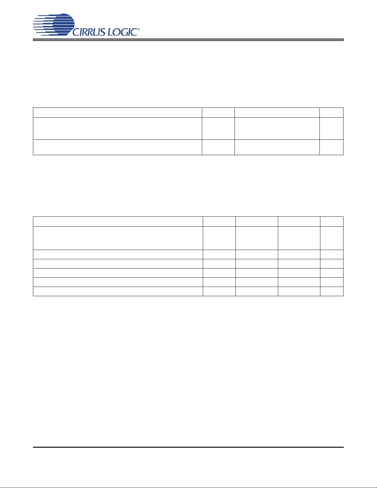
VA
3.3 V to 5 V
Single-Ended
Analog Input
Single-Ended
Analog Input
AINL
FILT+
VQ
AINR
Switch-Cap
ADC
Internal
Reference
Voltages
Switch-Cap
ADC
High-Pass
Filter
High-Pass
Filter
VD
3.3 V to 5 V
Low-Latency
Digital Filters
Low-Latency
Digital Filters
1.8 V to 5 V
Serial Port
VL
Auto-detect
MCLK Divider
Slave Mode
Auto-detect
M0
M1
Master Clock
SCLK
LRCK
SDOUT
Mode
Configuration
Reset
http://www.cirrus.com
Copyright © Cirrus Logic, Inc. 2008
(All Rights Reserved)
March '08
DS601F2
Page 2

Confidential Draft
TABLE OF CONTENTS
1. CHARACTERISTICS AND SPECIFICATIONS ...................................................................................... 4
SPECIFIED OPERATING CONDITIONS ............................................................................................... 4
ABSOLUTE MAXIMUM RATINGS ......................................................................................................... 4
ANALOG CHARACTERISTICS - COMMERCIAL GRADE .................................................................... 5
ANALOG CHARACTERISTICS - AUTOMOTIVE GRADE ..................................................................... 6
DIGITAL FILTER CHARACTERISTICS .................................................................................................7
DC ELECTRICAL CHARACTERISTICS ........................................... ... ... .... ... ... ... .... ... ......................... 10
DIGITAL CHARACTERISTICS ............................................................................................................. 10
SWITCHING CHARACTERISTICS - SERIAL AUDIO PORT ............................................ ... .... ... ......... 11
2. PIN DESCRIPTION .............................................................................................................................. 13
3. TYPICAL CONNECTION DIAGRAM ................................................................................................... 14
4. APPLICATIONS ................................................................................................................................... 15
4.1 Single-, Double-, and Quad-Speed Modes .....................................................................................15
4.2 Operation as Either a Clock Master or Slave .................................................................................15
4.2.1 Operation as a Clock Master . .......................................... ... ... ... .... ... ...................................... 16
4.2.2 Operation as a Clock Slave with Auto-Detect .......................... .... ... ... ... .... ... ... ... ... ................ 16
4.2.3 Master Clock ............................ ... .......................................................................................... 17
4.3 Serial Audio Interface ..................................................................................................................... 17
4.4 Power-Up Sequence ...................................................................................................................... 18
4.5 Analog Connections ....................................................................................................................... 18
4.6 Grounding and Power Supply Decoupling ...................... ... .... ... ... ... ... .... .........................................18
4.7 Synchronization of Multiple Devices ............................................................................................... 18
4.8 Capacitor Size on the Reference Pin (FILT+) ................................................................................19
5. PARAMETER DEFINITIONS ................................................................................................................ 20
6. PACKAGE DIMENSIONS ................................................................................................................... 21
THERMAL CHARACTERISTICS .......................................................................................................... 21
7. ORDERING INFORMATION ................................................................................................................ 22
8. REVISION HISTORY ............................................................................................................................ 22
3/11/08
CS5340
2 DS601F2
Page 3

Confidential Draft
LIST OF FIGURES
Figure 1.Single-Speed Mode Stopband Rejection ....................................... .... ... ... ..................................... 8
Figure 2.Single-Speed Mode Stopband Rejection ....................................... .... ... ... ..................................... 8
Figure 3.Single-Speed Mode Transition Band (Detail) ................................................................................ 8
Figure 4.Single-Speed Mode Passband Ripple .......................................................................................... 8
Figure 5.Double-Speed Mode Stopband Rejection ..................................................................................... 8
Figure 6.Double-Speed Mode Stopband Rejection ..................................................................................... 8
Figure 7.Double-Speed Mode Transition Band (Detail) .............................................................................. 9
Figure 8.Double-Speed Mode Passband Ripple ......................................................................................... 9
Figure 9.Quad-Speed Mode Stopband Rejection ....................................................................................... 9
Figure 10.Quad-Speed Mode Stopband Rejection ..................................................................................... 9
Figure 11.Quad-Speed Mode Transition Band (Detail) ............................................................................... 9
Figure 12.Quad-Speed Mode Passband Ripple .......................... .... ... ... ... ... .... ... ... ..................................... 9
Figure 13.Master Mode, Left-Justified SAI ................................................................................................ 12
Figure 14.Slave Mode, Left-Justified SAI .................................................................................................. 12
Figure 15.Master Mode, I²S SAI ................................................................................................................ 12
Figure 16.Slave Mode, I²S SAI .................................................................................................................. 12
Figure 17.Typical Connection Diagram ..................................................................................................... 14
Figure 18.CS5340 Master Mode Clocking ................................................................................................ 16
Figure 19.I²S Serial Audio Interface .......................................................................................................... 17
Figure 20.Left-Justified Serial Audio Interface .......................................................................................... 17
Figure 21.CS5340 Recommended Analog Input Buffer ............................................................................ 18
Figure 22.CS5340 THD+N versus Frequency .......................................................................................... 19
3/11/08
CS5340
LIST OF TABLES
Table 1. Speed Modes and the Associated Output Sample Rates (Fs) ................................. ... .... ... ... ... ... 15
Table 2. CS5340 Mode Control ................................................................................................................. 15
Table 3. Master Clock (MCLK) Ratios ....................................................................................................... 17
Table 4. Master Clock (MCLK) Frequencies for Standard Audio Sample Rates ...................................... 17
DS601F2 3
Page 4
Confidential Draft
3/11/08
CS5340
1. CHARACTERISTICS AND SPECIFICATIONS
(All Min/Max characteristics and specifications are guaranteed over the Specified Operating Conditions. Typical
performance characteristics and spe cif icat ion s ar e de riv e d from measurements taken at typical supply voltages
and T
= 25°C.)
A
SPECIFIED OPERATING CONDITIONS
(GND = 0 V, all voltages with respect to 0 V.)
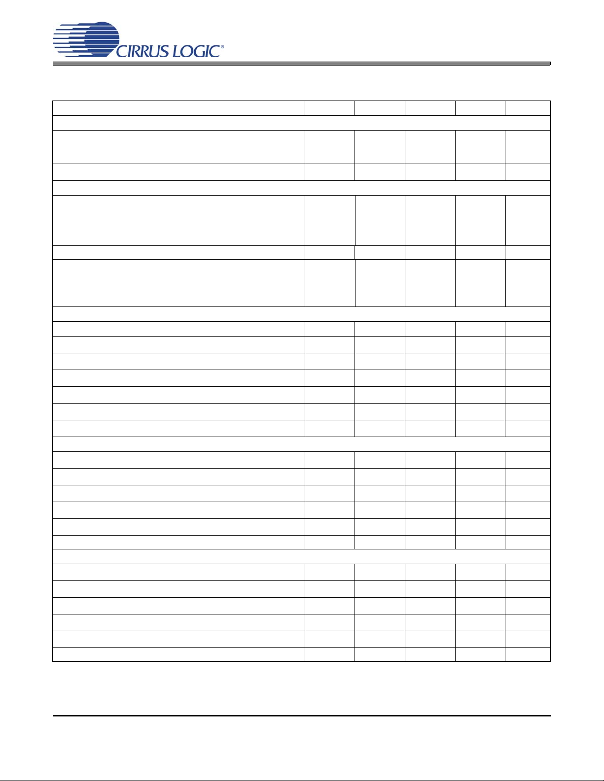
Parameter Symbol Min Typ Max Unit
Power Supplies Analog
Digital
Logic
Ambient Operating Temperature Commercial
Automotive
VA
VD
VL
T
T
AC
AC
3.1
3.1
1.7
-10
-40
(Note 1)
3.3
3.3
-
-
5.25
5.25
5.25
70
85
V
V
V
°C
°C
Notes:
1. This part is specified at typical analog vo ltages of 3. 3 V and 5. 0 V. See Ana log Ch arac terist ics - Commercial Grade and Analog Characteristics - Automotive Grade, below, for details.
ABSOLUTE MAXIMUM RATINGS
(GND = 0 V, All voltages with respect to ground.) (Note 2)
Parameter Symbol Min Max Units
DC Power Supplies: Analog
Logic
Digital
Input Current (Note 3)
Analog Input Voltage (Note 4)
Digital Input Voltage (Note 4)
Ambient Operating Temperature (Power Applied) T
Storage Temperature
V
T
2. Operation beyond these limits may result in permanent damage to the device.
Normal operation is not guaranteed at these extremes.
3. Any pin except supplies. Transient currents of up to ±100 mA on the analog input pins will not cause
SRC latch-up.
4. The maximum over/under voltage is limited by the input current.
VA
VL
VD
I
in
V
IND
stg
-0.3
-0.3
-0.3
+6.0
+6.0
+6.0
V
V
V
-10 +10 mA
IN
GND-0.7 VA+0.7 V
-0.7 VL+0.7 V
A
-50 +95
°C
-65 +150 °C
4 DS601F2
Page 5
Confidential Draft
3/11/08
CS5340
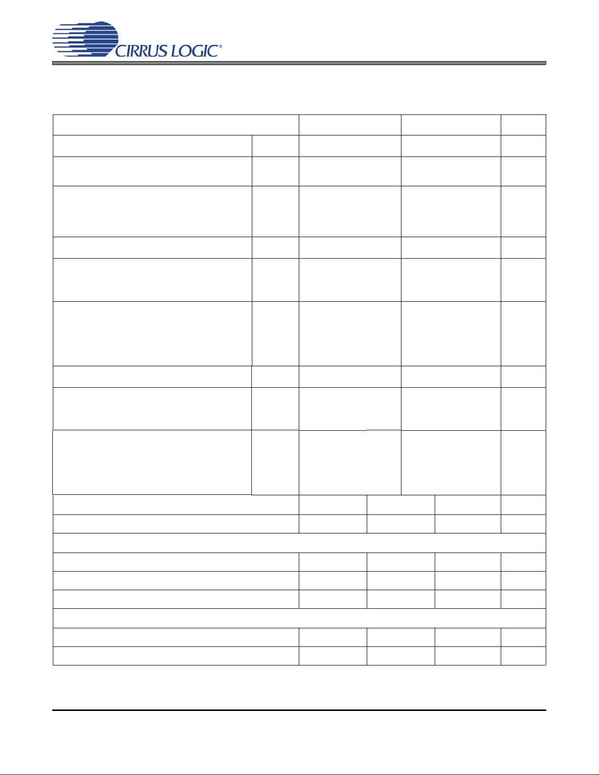
ANALOG CHARACTERISTICS - COMMERCIAL GRADE
Test Conditions (unless otherwise specified): Input test signal is a 1 kHz sine wave; measurement bandwidth is
10 Hz to 20 kHz.
Dynamic Performance for Commercial Grade VA = 5 V VA = 3.3 V
Single-Speed Mode Fs = 48 kHz
Dynamic Range A-weighted
unweighted
Total Harmonic Distortion + Noise (Note 5)
-1 dB
-20 dB
-60 dB
Double-Speed Mode Fs = 96 kHz
Dynamic Range A-weighted
unweighted
40 kHz bandwidth unweighted
Total Harmonic Distortion + Noise (Note 5)
-1 dB
-20 dB
-60 dB
40 kHz bandwidth -1 dB
Symbol Min Typ Max Min Typ Max Unit
95
92
THD+N
101
98
-
-
-
-94
-78
-38
-88
-
-
-
-
92
89
98
95
-
-91
-
-75
-
-35
-
-
-85
-
-
dB
dB
dB
dB
dB
Symbol Min Typ Max Min Typ Max Unit
95
92
THD+N
101
98
-
-
-
-
-
95
-94
-78
-38
-91
-88
-
-
-
-
-
-
92
89
98
95
-
-
-
-
-
92
-91
-75
-35
-85
-
-
-
-85
-
-
-
dB
dB
dB
dB
dB
dB
dB
Quad-Speed Mode Fs = 192 kHz
Dynamic Range A-weighted
unweighted
40 kHz bandwidth unweighted
Total Harmonic Distortion + Noise (Note 5)
-1 dB
-20 dB
-60 dB
40 kHz bandwidth -1 dB
Dynamic Performance All Modes
Interchannel Isolation - 90 - dB
Symbol Min Typ Max Min Typ Max Unit
95
92
THD+N
101
98
-
-
-
-
-
95
-94
-78
-38
-91
-88
-
-
-
-
-
-
92
89
98
95
-
-
-
-
-
92
-91
-75
-35
-85
Min Typ Max
-
-
-
-85
-
-
-
dB
dB
dB
dB
dB
dB
dB
Unit
DC Accuracy
Interchannel Gain Mismatch - 0.1 - dB
Gain Error -5 - +5 %
Gain Drift -
±100 - ppm/°C
Analog Input Characteristics
Full-Scale Input Voltage 0.53*VA 0.56*VA 0.59*VA Vpp
Input Impedance - 25 -
kΩ
5. Referred to the typical full-scale input voltage
DS601F2 5
Page 6
Confidential Draft
3/11/08
CS5340
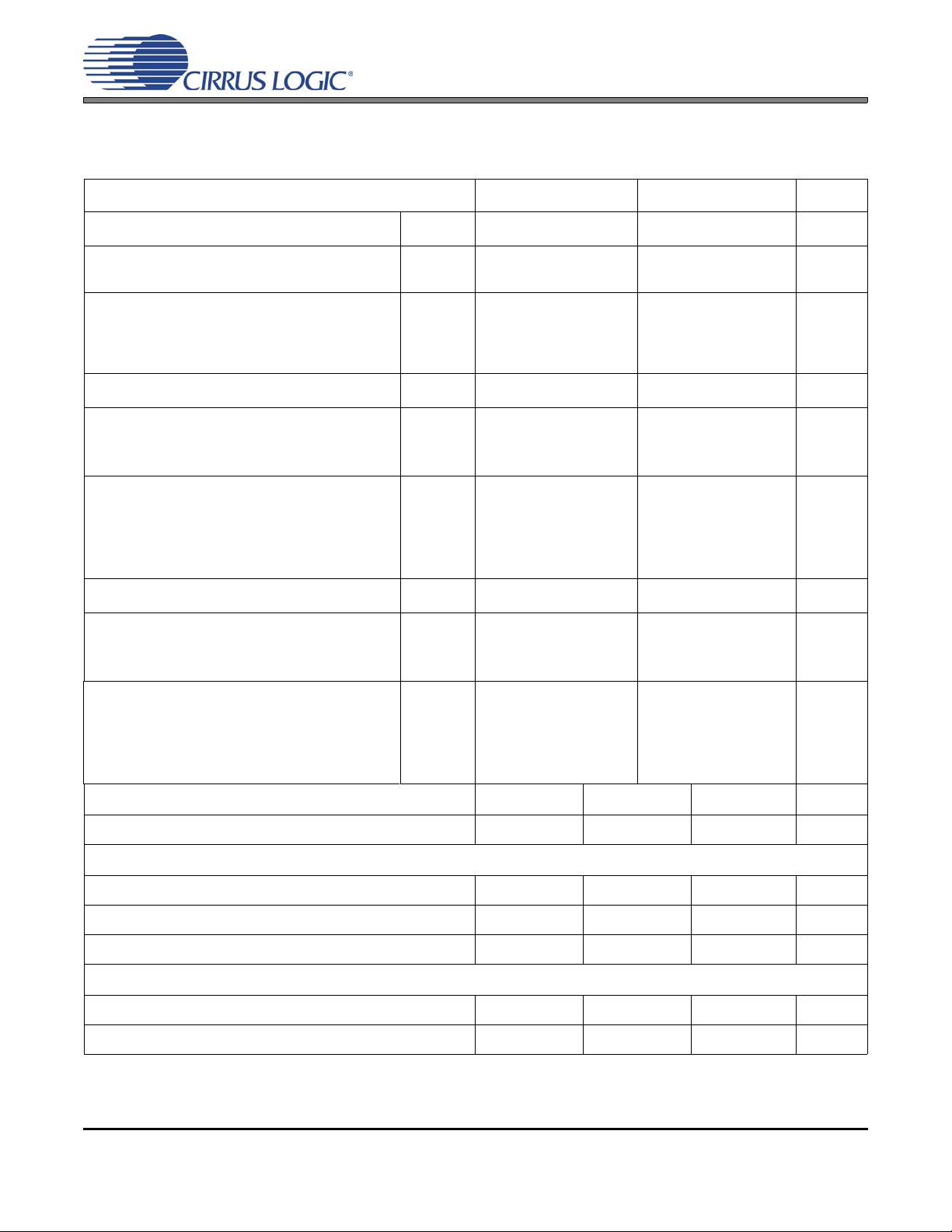
ANALOG CHARACTERISTICS - AUTOMOTIVE GRADE
Test Conditions (unless otherwise specified): Input test signal is a 1 kHz sine wave; measurement bandwidth is
10 Hz to 20 kHz.
Dynamic Performance for Automotive Grade VA = 5 V VA = 3.3 V
Single-Speed Mode Fs = 48 kHz
Dynamic Range A-weighted
unweighted
Total Harmonic Distortion + Noise (Note 5)
-1 dB
-20 dB
-60 dB
Double-Speed Mode Fs = 96 kHz
Dynamic Range A-weighted
unweighted
40 kHz bandwidth unweighted
Total Harmonic Distortion + Noise (Note 5)
-1 dB
-20 dB
-60 dB
40 kHz bandwidth -1 dB
Symbol Min Typ Max Min Typ Max Unit
93
90
THD+N
101
98
-
-
-
-94
-78
-38
-
-
-86
-
-
90
87
98
95
-
-91
-
-75
-
-35
-83
-
-
-
-
dB
dB
dB
dB
dB
Symbol Min Typ Max Min Typ Max Unit
93
90
THD+N
101
98
-
-
-
-
-
95
-94
-78
-38
-91
-
-
-
-86
-
-
-
90
87
98
95
-
-
-
-
-
92
-91
-75
-35
-85
-83
-
-
-
-
-
-
dB
dB
dB
dB
dB
dB
dB
Quad-Speed Mode Fs = 192 kHz
Dynamic Range A-weighted
unweighted
40 kHz bandwidth unweighted
Total Harmonic Distortion + Noise (Note 5)
-1 dB
-20 dB
-60 dB
40 kHz bandwidth -1 dB
Dynamic Performance All Modes
Interchannel Isolation - 90 - dB
Symbol Min Typ Max Min Typ Max Unit
93
90
THD+N
101
98
-
-
-
-
-
95
-94
-78
-38
-91
-
-
-
-86
-
-
-
90
87
98
95
-
-
-
-
-
92
-91
-75
-35
-85
Min Typ Max
-83
-
-
-
-
-
-
dB
dB
dB
dB
dB
dB
dB
Unit
DC Accuracy
Interchannel Gain Mismatch - 0.1 - dB
Gain Error -10 - +10 %
Gain Drift - ±100 - ppm/°C
Analog Input Characteristics
Full-Scale Input Voltage 0.50*VA 0.56 *VA 0.62*VA Vpp
Input Impedance - 25 -
kΩ
6. Referred to the typical full-scale input voltage
6 DS601F2
Page 7
Confidential Draft
3/11/08
CS5340
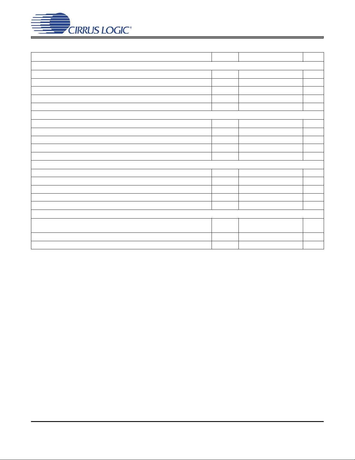
DIGITAL FILTER CHARACTERISTICS
Parameter Symbol Min Typ Max Unit
Single-Speed Mode
Passband (-0.1 dB) (Note 7) 0 - 0.4895 Fs
Passband Ripple -0.035 - 0.035 dB
Stopband (Note 7) 0.5687 - - Fs
Stopband Attenuation 70 - - dB
Total Group Delay (Fs = Output Sample Rate) t
gd
Double-Speed Mode
Passband (-0.1 dB) (Note 7) 0 - 0.4895 Fs
Passband Ripple -0.025 - 0.025 dB
Stopband (Note 7) 0.5604 - - Fs
Stopband Attenuation 69 - - dB
Total Group Delay (Fs = Output Sample Rate) t
gd
Quad-Speed Mode
Passband (-0.1 dB) (Note 7) 0 - 0.2604 Fs
Passband Ripple -0.025 - 0.025 dB
Stopband (Note 7) 0.5 - - Fs
Stopband Attenuation 60 - - dB
Total Group Delay (Fs = Output Sample Rate) t
gd
High-Pass Filter Characteristics
Frequency Response -3.0 dB
-0.13 dB (Note 8)
Phase Deviation @ 20 Hz (Note 8) -10 -Deg
Passband Ripple -- 0dB
-12/Fs - s
-9/Fs - s
-5/Fs - s
-120-
-
Hz
Hz
7. Filter characteristics scale precisely with Fs
8. Response shown is for Fs equal to 48 kHz. Filter characteristics scale with Fs.
DS601F2 7
Page 8

Confidential Draft
0
0
0
-10
-20
-30
-40
-50
-60
-70
-80
-90
-100
Amplitude (dB)
-110
-120
-130
-140
0.0 0.1 0.2 0.3 0.4 0.5 0.6 0.7 0.8 0.9 1.0
Frequency (normalized to Fs)
3/11/08
Amplitude (dB)
-10
-20
-30
-40
-50
-60
-70
-80
-90
-100
-110
-120
-130
-140
0.40 0.42 0.44 0.46 0.48 0.50 0.52 0.54 0.56 0.58 0.60
Frequency (normalized to Fs)
CS5340
Figure 1. Single-Speed Mode Stopband Rejection Figure 2. Single-Speed Mode Stopband Rejection
0
-1
-2
-3
-4
-5
-6
-7
Amplitude (dB)
-8
-9
-10
0.45 0.46 0.47 0.48 0.49 0.5 0.51 0.52 0.53 0.54 0.55
Frequency (normalized to Fs)
0.10
0.08
0.06
0.04
0.02
0.00
-0.02
-0.04
Amplitude (dB)
-0.06
-0.08
-0.10
0 0.05 0.1 0.1 5 0.2 0.25 0.3 0.35 0.4 0.45 0.5
Frequency (normalized to Fs)
Figure 3. Single-Speed Mode Transition Band (Detail) Figure 4. Single-Speed Mode Passband Ripple
-10
-20
-30
-40
-50
-60
-70
-80
-90
-100
Amplitude (dB)
-110
-120
-130
-140
0.0 0.1 0.2 0.3 0.4 0.5 0.6 0.7 0.8 0.9 1.0
Frequency (normalized to Fs)
0
-10
-20
-30
-40
-50
-60
-70
-80
-90
-100
Amplitude (dB)
-110
-120
-130
-140
0.40 0.42 0.44 0.46 0.48 0.50 0.52 0.54 0.56 0.58 0.60
Frequency (normalized to Fs)
Figure 5. Double-Speed Mode Stopband Rejection Figure 6. Double-Speed Mode Stopband Reject ion
8 DS601F2
Page 9

Confidential Draft
0
0
-1
-2
-3
-4
-5
-6
-7
Amplitude (dB)
-8
-9
-10
0.46 0.47 0.48 0.49 0.50 0.51 0.52
Frequency (normalized to Fs)
3/11/08
Amplitude (dB)
0.10
0.08
0.06
0.04
0.02
0.00
-0.02
-0.04
-0.06
-0.08
-0.10
0.00 0.05 0.10 0.15 0.20 0.25 0.30 0.35 0.40 0.45 0.50
Frequency (normalized to Fs)
CS5340
Figure 7. Double-Speed Mode Transition Band (Detail) Figure 8. Double-Speed Mode Passband Ripple
-10
-20
-30
-40
-50
-60
-70
-80
-90
-100
Amplitude (dB)
-110
-120
-130
-140
0.0 0.1 0.2 0.3 0.4 0.5 0.6 0.7 0.8 0.9 1.0
Frequency (normalized to Fs)
0
-10
-20
-30
-40
-50
-60
-70
-80
-90
-100
Amplitude (dB)
-110
-120
-130
-140
0.20 0.25 0.30 0.35 0.40 0.45 0.50 0.55 0.60 0.65 0.70 0.75 0.80 0.85
Frequency (normalized to Fs)
Figure 9. Quad-Speed Mode Stopband Rejection Figure 10. Quad-Speed Mode Stopband Rejection
0
-1
-2
-3
-4
-5
-6
-7
Amplitude (dB)
-8
-9
-10
0.10 0.15 0.20 0.25 0.30 0.35 0.40 0.45 0.50
Frequency (normalized to Fs)
0.10
0.08
0.06
0.04
0.02
0.00
-0.02
-0.04
Amplitude (dB)
-0.06
-0.08
-0.10
0.00 0.03 0.05 0.08 0.10 0 .13 0.15 0.18 0.20 0.23 0.25 0.28
Frequency (normalized to Fs)
Figure 11. Quad-Speed Mode Transition Band (Detail) Figure 12. Quad-Speed Mode Passband Ripple
DS601F2 9
Page 10

Confidential Draft
3/11/08
DC ELECTRICAL CHARACTERISTICS
(GND = 0 V, all voltages with respect to 0 V. MCLK=12.288 MHz; Master Mode)
Parameter Symbol Min Typ Max Unit
DC Power Supplies: Positive Analog
Positive Digital
Positive Logic
Power Supply Current VA = 5 V
(Normal Operation) VA = 3.3 V
VL,VD = 5 V
VL,VD = 3.3 V
Power Supply Current VA = 5 V
(Power-Down Mode) (Note 9) VL,VD=5 V
Power Consumption VL, VD, VA = 5 V
(Normal Operation) VL, VD, VA = 3.3 V
(Power-Down Mode)
Power Supply Rejection Ratio (1 kHz) (Note 10)
V
Nominal Voltage
Q
Output Impedance
Filt+ Nominal Voltage
Output Impedance
Maximum allowable DC current source/sink
VA
VD
VL
I
A
I
A
I
D
I
D
I
A
I
D
-
-
-
PSRR - 65 - dB
3.1
3.1
1.7
CS5340
-
-
-
-
-
-
-
-
-
-
-
-
-
-
-
-
-
21
18.2
15
9
1.5
0.4
180
90
9.5
VA÷2
25
VA
36
0.01
5.25
5.25
5.25
25.5
22.5
18.5
10
-
-
220
107.2
-
-
-
-
-
-
V
V
V
mA
mA
mA
mA
mA
mA
mW
mW
mW
V
kΩ
V
kΩ
mA
9. Power Down Mode is defined as RST
= Low, with all clocks and data lines held static at a valid logic
levels.
10. V alid with the recommende d capacitor values on FILT+ and VQ as shown in the Typical Connection
Diagram, Figure 17 on page 14.
DIGITAL CHARACTERISTICS
Parameter Symbol Min Typ Max Units
High-Level Input Voltage (% of VL) V
Low-Level Input Voltage (% of VL) V
High-Level Output Voltage at Io = 100 µA(% of VL)
Low-Level Output Voltage at I
Input Leakage Current I
=100 µA(% of VL)
o
IH
IL
V
OH
V
OL
in
70% - - V
--30%V
70% - - V
--15%V
-10 - +10 µA
10 DS601F2
Page 11
Confidential Draft
3/11/08
CS5340
SWITCHING CHARACTERISTICS - SERIAL AUDIO PORT
(Logic "0" = GND = 0 V; Logic "1" = VL, CL = 20 pF)
Parameter Symbol Min Typ Max Unit
MCLK Specifications
MCLK Period
MCLK Pulse Duty Cycle
t
clkw
Master Mode
SCLK falling to LRCK Single-Speed
Double-Speed
Quad-Speed
SCLK falling to SDOUT valid. t
SCLK Duty Cycle. Single-Speed - 50 - %
Double-Speed
Quad-Speed
t
mslr
sdo
Slave Mode
Single-Speed (Note 11)
LRCK Duty Cycle
SCLK Period
SCLK Duty Cycle
SDOUT valid before SCLK rising
SDOUT valid after SCLK rising
SCLK falling to LRCK edge
t
sclkw
t
stp
t
hld
t
slrd
Double-Speed (Note 11)
LRCK Duty Cycle
SCLK Period
SCLK Duty Cycle
SDOUT valid before SCLK rising
SDOUT valid after SCLK rising
SCLK falling to LRCK edge. t
t
sclkw
t
stp
t
hld
slrd
Quad-Speed (Note 11)
LRCK Duty Cycle
SCLK Period
SCLK Duty Cycle
SDOUT valid before SCLK rising
SDOUT valid after SCLK rising
SCLK falling to LRCK edge. t
t
sclkw
t
stp
t
hld
slrd
39 - 45 ns
78 - 1953 ns
40 - 60 %
-20 - 20 ns
-20 - 20 ns
-8 - 8 ns
- - 32 ns
-50-%
-33-%
40 50 60 %
156 - - ns
45 50 55 %
10 - - ns
5--ns
-20 - 20 ns
40 50 60 %
156 - - ns
45 50 55 %
10 - - ns
5--ns
-20 - 20 ns
40 50 60 %
78 - - ns
29.7 33 50 %
10 - - ns
5--ns
-8 - 8 ns
11. For a description of speed modes, please refer to Table on page 15.
DS601F2 11
Page 12

Confidential Draft
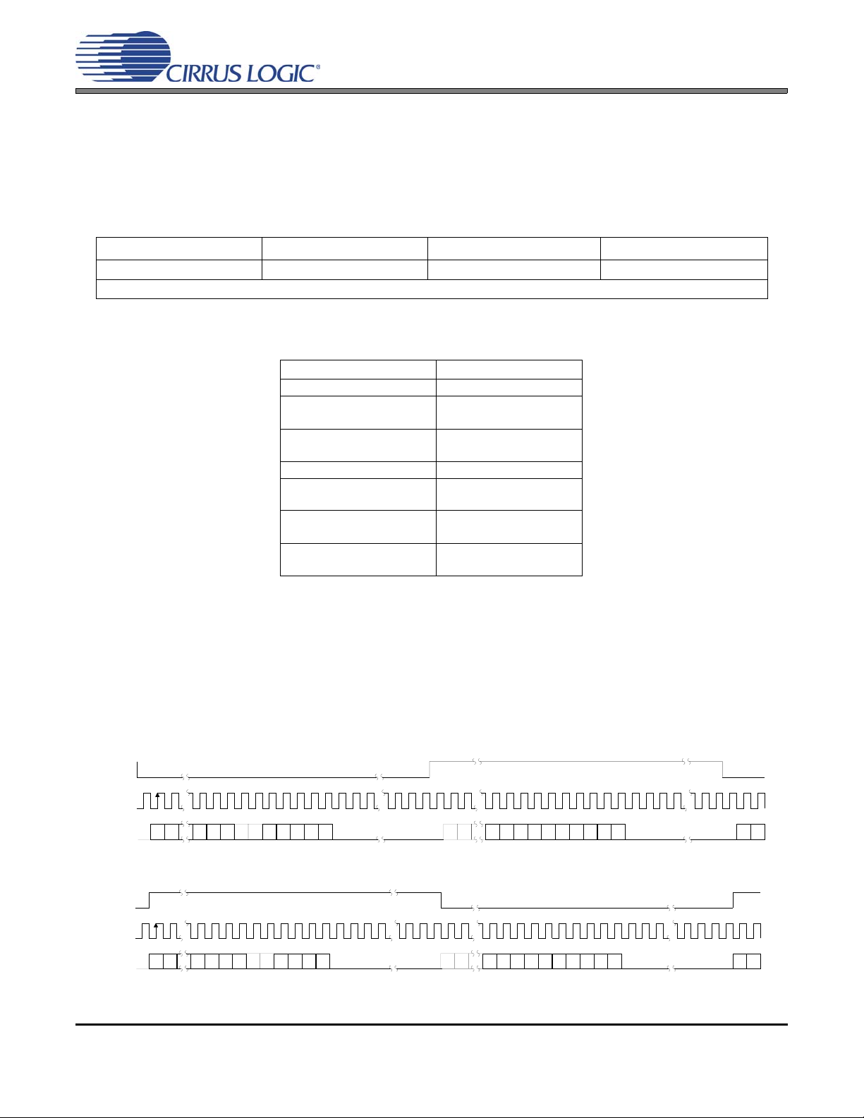
SCLK output
LRCK output
SDOUT
Figure 13. Master Mode, Left-Justified SAI Figure 14. Slave Mode, Left-Justified SAI
SCLK output
LRCK output
SDOUT
t
mslr
t
sdo
MSB MSB-1
t
mslr
t
MSB
sdo
3/11/08
LRCK input
SCLK input
SDOUT
LRCK input
SCLK input
SDOUT
t
slrd
t
slrd
CS5340
t
sclkw
t
t
hld
stp
MSB
t
sclkw
MSB-1
t
stp
MSB
t
hld
Figure 15. Master Mode, I²S SAI Figure 16. Slave Mode, I²S SAI
12 DS601F2
Page 13

Confidential Draft
3/11/08
CS5340
2. PIN DESCRIPTION
M0 M1
MCLK FILT+
VL REF_GND
SDOUT VA
GND AINR
VD VQ
SCLK AINL
LRCK RST
Pin Name # Pin Description
M0
M1
MCLK 2 Master Clock (Input) - Clock source for the delta-sigma modulator and digital filters.
VL 3 Logic Power (Input) - Positive power for the digital input/output.
SDOUT 4 Serial Audio Data Output (Output) - Output for two’s complement serial audio data.
GND 5,14 Ground (Input) - Ground reference. Must be connected to analog ground.
VD 6 Digital Power (Input) - Positive power supply for the digital section.
SCLK 7 Serial Clock (Input/Output) - Serial clock for the serial audio interface.
LRCK 8
RST
AINL
AINR
VQ 11
VA 13 Analog Power (Input) - Positive power supply for the analog section.
FILT+ 15
1
16
9 Reset (Input) - The device enters a low power mode when low.
10
12
Mode Selection (Input) - Determines the operational mode of the device.
Left Right Clock (Input/Output) - Determines which channel, Left or Right, is currently
active on the serial audio data line.
Analog Input (Input) - The full-scale analog input level is specified in the Analog Charac-
teristics specification table.
Quiescent Volt age (Output) - Filter connection for the internal quiescent
reference voltage.
Positive Voltage Reference (Output) - Positive reference voltage for the internal
sampling circuits.
1
1
1
1
2
2
2
2
3
3
4
4
5
5
5
5
6
6
6
6
7
7
8
8
16
16
15
15
14
14
13
13
12
12
11
11
10
10
9
9
DS601F2 13
Page 14

Confidential Draft
3. TYPICAL CONNECTION DIAGRAM
3.3V to 5V
3.3V to 5V
µ
1
+
Analog Input Buffer
Figure 21
+
1µF
+
1µF
***
+
F
0.1µF
0.1µF
0.1µF
FILT+
VA
5.1
**
Ω
D
V
REFGND
1µ
0.1µF
F
VQ
CS5340
A/D CONVERTER
AINL
AINR
3/11/08
0.1µF
V
0.1µF
L
RST
SDOUT
M0
M1
+
VL or GND
10k
Ω
CS5340
1.8 V to 5V
1µF
Power Down
and Mode
Settin g s
*
Audio Data
Processor
GND
MCLK
LRCK
SCLK
* Pull-up to VL for I2S
Pull-down to GND for LJ
** Resistor may only be
used if VD is derived from
VA. If used, do not drive
any other logic from VD
Timing Logic
and Clock
*** Cap a c ito r v a lue a ff ec ts
low frequency distortion
performance as described
in Section 4.8
14 DS601F2
Page 15
Confidential Draft
3/11/08
4. APPLICATIONS
4.1 Single-, Double-, and Quad-Speed Modes
The CS5340 can support outpu t sample rates from 2 kHz to 200 kHz. The prop er spee d mode can be de termined by the desired output sample rate and the external MCLK/LRCK ratio, as shown in Table 1.
Speed Mode
Single-Speed Mode
Double-Speed Mode
Quad-Speed Mode
* Quad-Speed Mode, 64x only available in Master Mode.
Table 1. S peed Modes and the Associated Output Sample Rates (Fs)
4.2 Operation as Either a Clock Master or Slave
MCLK/LRCK
Ratio
512x 43 - 50
256x 2 - 50
256x 86 - 100
128x 4 - 100
128x 172 - 200
64x* 100 - 200
CS5340
Output Sample Rate Range (kHz)
The CS5340 supports operation as either a clock master or slave. As a clock master, the LRCK and SCLK
pins are outputs with the left/right and serial clocks synchronously generated on-chip. As a clock slave, the
LRCK and SCLK pins are inputs and require the left/right and serial clocks to be externally generated. The
selection of clock master or slave is made via the Mode pins as shown in Table 2.
M1 (Pin 16) M0 (Pin 1) MODE
00
01
10
11
T able 2. CS5340 Mode Control
Clock Master, Single-Speed Mode
Clock Master, Double-Speed Mode
Clock Master, Quad-Speed Mode
Clock Slave, All Speed Modes
DS601F2 15
Page 16
Confidential Draft
4.2.1 Operation as a Clock Master
As a clock master, LRCK and SCLK operate as outputs. The left/right and serial clocks are internally derived from the master clock with the left/right clock equal to Fs and the serial clock equal to 64x Fs, as
shown in Figure 18.
MCLK
÷ 1
÷ 2
0
1
3/11/08
÷ 256
÷ 128
÷ 64
÷ 4
Single
Speed
Double
Speed
Quad
Speed
Single
Speed
00
01
10
00
CS5340
LRCK Output
(Equal to Fs)
M0M1
Auto-Select
Figure 18. CS5340 Master Mode Clocking
4.2.2 Operation as a Clock Slave with Auto-Detect
LRCK and SCLK operate as inputs in clock slave mode. It is recommended that the left/right clock be
synchronously derived from the master clock and must be equal to Fs. It is also recommended that the
serial clock be synchronously derived from the master clock and be equal to 64x Fs to maximize system
performance.
A unique feature of the CS5340 is the automatic selection of either Single-, Double- or Quad-Speed mode
when operating as a clock slave. The auto-mode select feature negates the need to configure the Mode
pins to correspond to the desired mode. The auto-mode selection feature supports all standard audio
sample rates from 2 to 200 kHz. However, there are ranges of non-standard audio sample rates that are
not supported when operating with a fast MCLK (512x, 256x, 128x for Single-, Do uble-, and Quad -Speed
Modes, respectively). Please refer to Table for supported sample rate ranges.
÷ 2
÷ 1
Double
Speed
Quad
Speed
01
10
SCLK Output
16 DS601F2
Page 17
Confidential Draft
3/11/08
4.2.3 Master Clock
The CS5340 requires a Master clock (MCLK) which runs the internal sampling circuits and digital filters.
There is also an internal MCLK divider which is automatically activated based on the speed mode and
frequency of the MCLK. Table 3 shows a listing of the external MCLK/LRCK ratios that are required.
Table 4 lists some comm on audio output sample rates and th e required MCLK frequency. Please note
that not all of the listed sample rates are supported when operating with a fast MCLK (512x, 256x, 128x
for Single-, Double-, and Quad-Speed Modes, respectively).
Single-Speed Mode Double-Speed Mode Quad-Speed Mode
MCLK/LRCK Ratio 256x, 512x 128x, 256x 64x*,128x
* Quad Speed, 64x only available in Master Mode.
T able 3. Master Clock (MCLK) Ratios
SAMPLE RATE (kHz) MCLK (MHz)
32 8.192
44.1 11.2896
22.5792
48 12.288
24.576
64 8.192
88.2 11.2896
22.5792
96 12.288
24.576
192 12.288
24.576
Table 4. Master Clock (MCLK) Frequencies for Standard Audio Sample Rates
CS5340
4.3 Serial Audio Interface
The CS5340 supports both I²S and Left-Justified serial audio formats. Upon start-up, the CS5340 will detect
the logic level on SDOUT (pin 4). A 10 kΩ pull-up to VL is needed to select I²S format, and a 10 kΩ pulldown to GND is needed to select Left-Justified format. Figures 19 and 20 illustrate the I²S and Left-Justified
audio formats. Please see Figures 13 through 16, for more information on the required timing for the two
serial audio interface formats. Also see Application Note AN28 2 for a detaile d discussion o f the serial aud io
interface formats.
LRC K
SCLK
SDATA 23 22 8 7 23 22
LRCK
SCLK
SDATA 23 22 7 6 23 22
Left Channel Right Channel
23 226543210 8765432109 9
Figure 19. I²S Serial Audio Interface
Left Channel Right Channel
23 225432108 7654321089 9
Figure 20. Left-Justified Serial Audio Interface
DS601F2 17
Page 18
Confidential Draft
4.4 Power-Up Sequence
Reliable power-up can be accomplished by keeping the device in reset until the power supplies, clocks and
configuration pins are stable. It is also recommended that reset be enabled if the analog or digital supplies
drop below the minimum specified operating voltages to prevent power-glitch-related issues.
4.5 Analog Connections
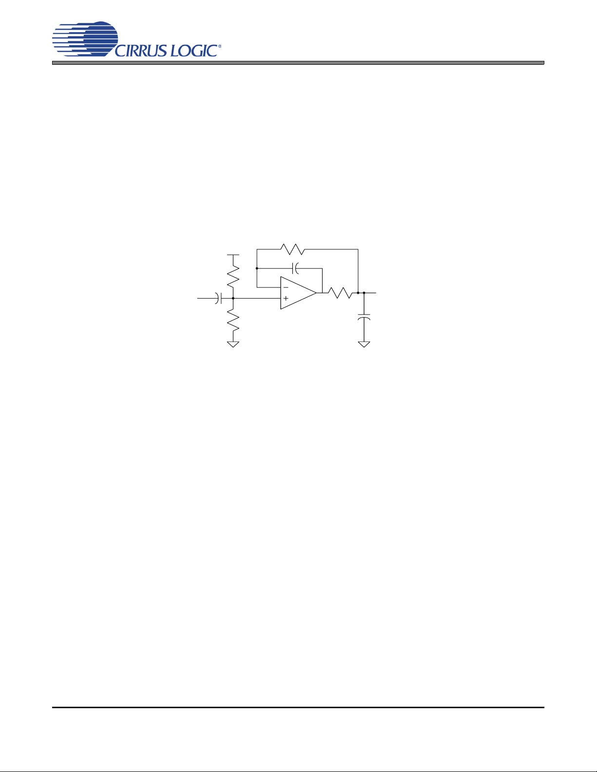
The analog modulator samples the input at half of the MCLK frequency, or nominally 6.144MHz. The digital
filter will reject signals within the stopband of the filter. However, there is no rejection for input signals which
are multiples of the input sampling frequency (n
shows the suggested filter that will attenuate any noise energy at 6.144 MHz, in addition to providing the
optimum source impedance for the modulators. The use of capacitors which have a large voltage coefficient
(such as general purpose ceramics ) m ust be av oided since these can degrade signal linearity.
AINx
100 kΩ
4.7 µF
100 kΩ
VA
3/11/08
CS5340
× 6.144 MHz), where n=0,1,2,... Refer to Figure 21 which
634 Ω
470 pF
C0G
91 Ω
CS5340 AINx
2700 pF
Figure 21. CS5340 Recommended Analog Input Buffer
4.6 Grounding and Power Supply Decoupling
As with any high-resolution converter, achieving optimal performance from the CS5340 requires carefu l attention to power supply and grounding arrangements. Figure 17 shows the recommended power arrangements, with VA and VL connected to clean supplies. VD, which powers the digital filter, may be run from the
system logic supply or may be powered from the analog supply via a resistor. In this case, no additional
devices should be powered from VD. Decoupling capacito rs should be as near to the ADC as possible, with
the low-value ceramic capacitor being the nearest. All signals, especially clocks, should be kept away from
the FILT+ and VQ pins in order to avoid unwanted cou pling into the modu lators. The FILT+ a nd VQ decoupling capacitors, particularly the 0.01 µF, must be positioned to minimize the electrical path from FILT+ and
REF_GND. Furthermore, all ground pins on CS5340 should be referenced to the same ground reference.
The CDB5340 evaluation board demonstrates the optim um layout and power supply arr angements. To minimize digital noise, connect the ADC digital outputs only to CMOS inputs.
4.7 Synchronization of Multiple Devices
In systems where multiple ADCs are required, the user can a chieve simultaneous sampling if the MCLK and
LRCK signals are the same for all of the CS5340’s in the system. If only one master clock source is needed,
one solution is to place one CS5340 in Master mode, and slave all of the othe r CS5340’s to the one master.
If multiple master clock sources are needed, a possible solution would be to supply all clocks from the same
external source and time the CS5340 reset with the inactive (falling) edge of MCLK. This will ensure that all
converters begin sampling on the same clock edge.
18 DS601F2
Page 19

Confidential Draft
3/11/08
4.8 Capacitor Size on the Reference Pin (FILT+)
The CS5340 requires an external capacitance on the internal reference voltage pin, FILT+. The size of this
decoupling capacitor will affect the low frequency distortion performance as shown in Figure 22, with larger
capacitor values used to optimize low frequency distortion performance. This plot was taken using the
CDB5340 evaluation platform, with the device running in Single-Speed Mode and VA=VD=VL=5 V.
1 uF
2.2 uF
3.3 uF
4.7 uF
5.6 uF
6.8 uF
10 uF
47 uF
22 uF
CS5340
100 uF
Figure 22. CS5340 THD+N versus Frequency
DS601F2 19
Page 20

Confidential Draft
5. PARAMETER DEFINITIONS
Dynamic Range
The ratio of the rms value of the signal t o the rms su m of all other spectral components over the specified
bandwidth. Dynamic Range is a signal-to-noise ratio measurement over the specified bandwidth made with
a -60 dBFS signal. 60 dB is added to resulting measurement to refer the measurement to full-scale. This
technique ensures that the distortion components are below the noise level and do not affect the measurement. This measurement technique has been accepted by the Audio Engineering Society, AES17-1991,
and the Electronic Industries Association of Japan, EIAJ CP-307. Expressed in decibels.
Total Harmonic Distortion + Noise
The ratio of the rms value of the signal t o the rms su m of all other spectral components over the specified
bandwidth (typically 10 Hz to 20 kHz), including distortion components. Expressed in decibels. Measured
at -1 and -20 dBFS as suggested in AES17-1991 Annex A.
Frequency Response
A measure of the amplitude r es po ns e va riatio n from 10 Hz to 20 kHz relative to the amplitude r es po ns e at
1 kHz. Units in decibels.
Interchannel Isolation
A measure of crosstalk between the left and right channels. Measured for each channel at the converter's
output with no signal to the input under test and a full-scale signal applied to the other channel. Units in decibels.
3/11/08
CS5340
Interchannel Gain Mismatch
The gain difference between left and right channels. Units in decibels.
Gain Error
The deviation from the nominal full-scale analog input for a full-scale digital output.
Gain Drift
The change in gain value with temperature. Units in ppm/°C.
Offset Error
The deviation of the mid-scale transition (111...111 to 000...000) from the ideal. Units in mV.
20 DS601F2
Page 21
Confidential Draft
3/11/08
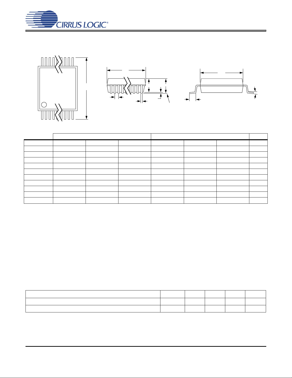
6. PACKAGE DIMENSIONS 16L TSSOP (4.4 mm BODY) PACKAGE DRAWING
N
D
1
23
TOP VIEW
E
e
2
b
SIDE VIEW
A2
A1
A
SEATING
PLANE
L
INCHES MILLIMETERS NOTE
DIM MIN NOM MAX MIN NOM MAX
A -- -- 0.043 -- -- 1.10
A1 0.002 0.004 0.006 0.05 -- 0.15
A2 0.03346 0.0354 0.037 0.85 0.90 0.95
b 0.00748 0.0096 0.012 0.19 0.245 0.30 2,3
D 0.193 0.1969 0.201 4.90 5.00 5.10 1
E 0.248 0.2519 0.256 6.30 6.40 6.50
E1 0.169 0.1732 0.177 4.30 4.40 4.50 1
e -- 0.026 BSC -- -- 0.65 BSC --
L 0.020 0.024 0.028 0.50 0.60 0.70
µ
0° 4° 8° 0° 4° 8°
1
E1
END VIEW
CS5340
∝
JEDEC #: MO-153
Controlling Dimension is Millimeters
1. “D” and “E1” are reference datums and do not included mold flash or protrusions, but do include mold
mismatch and are measured at the parting line, mold flash or protrusions shall not exceed 0.20 mm per
side.
2. Dimension “b” does not include dambar protrusion/intrusion. Allowable dambar protrusion shall be
0.13 mm total in excess of “b” dimension at maximum material condition. Dambar intrusion shall not reduce dimension “b” by more than 0.07 mm at least material condition.
3. These dimensions apply to the flat section of the lead between 0.10 and 0.25 mm from lead tips.
THERMAL CHARACTERISTICS
Parameter Symbol Min Typ Max Unit
Allowable Junction Temperatu re - - 135
Junction to Ambient Thermal Impedance θ
JA
-75-
DS601F2 21
°C
°C/W
Page 22

Confidential Draft
3/11/08
CS5340
7. ORDERING INFORMATION
Product Description Package Pb-Free Grade Temp Range Container Order #
CS5340
CS5340
CDB5340 CS5340 Evaluation Board - - - - - CDB5340
101 dB, 192 kHz, Multi-Bit
Audio A/D Converter
101 dB, 192 kHz, Multi-Bit
Audio A/D Converter
16-TSSOP YES Commercial -10° to +70° C
16-TSSOP YES Automotive -40° to +85° C
Bulk CS5340-CZZ
Tape & Reel CS5340-CZZR
Bulk CS5340-DZZ
Tape & Reel CS5340-DZZR
8. REVISION HISTORY
Release Changes
Remove CS5340-CZ from Ordering Information
PP3
F1
F2
Redefine Serial Audio Port Switching Characteristics
Correct dimension “e” under Package Dimensions
Update Output Sample Rate Range
Update maximum current and power specifications
Update Filt+ output impedance specification
Reduced minimum sample rate to 4 kHz for Double-Speed Mode 128x in Table 1 on page 15
Updated Legal Text
Contacting Cirrus Logic Support
For all product questions and inquiries, contact a Cirrus Logic Sales Representative.
To find the one nearest to you, go to www.cirrus.com.
IMPORTANT NOTICE
Cirrus Logic, Inc. and its subsidiaries ("Cirrus") believe that the information contained in this document is accurate and reliable. However, the information is subject
to change without not ice and is pr ovided "AS IS" witho ut warr anty of any kind (express or implied). Customers are advised to obtain the latest version of relevant
information to verify, before placing orders, that information being relied on is current and complete. All products are sold subject to the terms and conditions of sale
supplied at the time of order acknowledgment, including those pertaining to warranty, indemnification, and limitation of liability. No responsibility is assumed by Cirrus
for the use of this information, including use of this information as the basis for manufacture or sale of any items, or for infringement of patents or other rights of third
parties. This document is the property of Cirrus and by furnishing this information, Cirrus grants no license, express or implied under any patents, mask work rights,
copyrights, trademarks, trade secrets or other inte llectual property rig hts. Cirrus owns the copyrights associated with the information contained herein and gives consent for copies to be made of the information only for use within your organization with respect to Cirrus integrated circuits or other products of Cirrus. This consent
does not extend to other copying such as copying for general distribution, advertising or promotional purposes, or for creating any work for resale.
CERTAIN APPLICATIONS USING SEMICONDUCTOR PRODUCTS MAY INVOLVE POTENTIAL RISKS OF DEATH, PERSONAL I NJURY, OR SEVERE PROPERTY OR ENVIRONMENTAL DAMAGE (“CRITICAL APPLICATIONS”). CIRRUS PRODUCTS ARE NOT DESIGNED, AUTHORIZED OR WARRANTED FOR USE
IN PRODUCTS SURGICALLY IMPLANTED INTO THE BODY, AUTOMOTIVE SAFETY OR SECURITY DEVICES, LIFE SUPPORT PRODUCTS OR OTHER CRITICAL APPLICATIONS. INCLUSION OF CIRRUS PRODUCTS IN SUCH APPLICATIONS IS UNDERSTOOD TO BE FULLY AT THE CUSTOMER’S RISK AND
CIRRUS DISCLAIMS AND MAKES NO WARRANTY, EXPRESS, STATUTORY OR IMPLIED, INCLUDING THE IMPLIED WARRANTIES OF MERCHANTABILITY
AND FITNESS FOR PARTICULAR PURPOSE, WITH REGARD TO ANY CIRRUS PRODUCT THAT IS US ED IN SUCH A MANNER. IF THE CUSTOMER OR
CUSTOMER’S CUSTOMER USES OR PERMITS THE USE OF CIRRUS PRODUCTS IN CRITICAL APPLICATIONS, CUSTOMER AGREES, BY SUCH USE, TO
FULLY INDEMNIFY CIRRUS, ITS OFFICERS, DIRECTORS, EMPLOYEES, DISTRIB UTORS A ND OTHER AGENTS FROM ANY AND ALL LIA BIL I TY, I NCLUDING ATTORNEYS’ FEES AND COSTS, THAT MA Y RE S ULT FROM OR ARISE IN CONNECTION WITH THESE USES .
Cirrus Logic, Cirrus, and the Cirrus Logic logo designs are trademarks of Cirrus Logic, Inc. All other brand and product names in this document may be trademarks
or service marks of their respective owners.
22 DS601F2
 Loading...