

CS5330A
CS5331A
8-Pin, Stereo A/D Converter for Digital Audio
Features
Single +5 V Power Supply
•
18-Bit Resolution
•
94 dB Dynamic Range
•
Linear Phase Digital Anti-Alias Filtering
•
0.05dB Passband Ripple
80dB Stopband Rejection
Low Power Dissipation: 150 mW
•
Power-Down Mode for Portable
Applications
Complete CMOS Stereo A/D System
•
Delta-Sigma A/D Converters
Digital Anti-Alias Filtering
S/H Circuitry and Voltage Reference
Adjustable System Sampling Rates
•
including 32kHz, 44.1 kHz & 48kHz
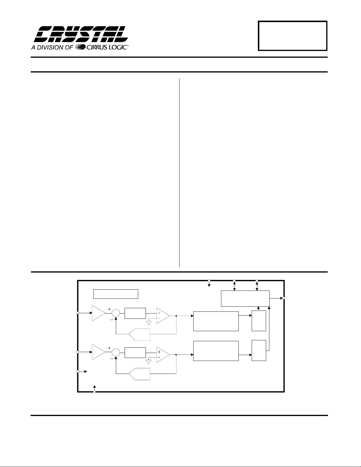
General Description
The CS5330A / 31A is a complete stereo analog-todigital converter which performs anti-alias filtering,
sampling and analog-to-digital conversion generating
18-bit values for both left and right inputs in serial form.
The output sample rate can be infinitely adjusted between 2 and 50 kHz.
The CS5330A / 31A operates from a single +5V supply
and requires only 150 mW for normal operation, making it ideal for battery-powered applications.
The ADC uses delta-sigma modulation with 128X oversampling, followed by digital filtering and decimation,
which removes the need for an external anti-alias filter.
The linear-phase digital filter has a passband to
21.7 kHz, 0.05 dB passband ripple and >80 dB stopband rejection. The device also contains a high pass
filter to remove DC offsets .
The device is available in a 0.208" wide, 8-pin surface
mount package.
ORDERING INFORMATION:
Model Temp. Range Package Type
CS5330A-KS -10° to 70°C 8-pin plastic SOIC
CS5331A-KS -10° to 70°C 8-pin plastic SOIC
CS5330A-BS-40° to +85°C8-pin plastic SOIC
CS5331A-BS-40° to +85°C8-pin plastic SOIC
Voltage Reference
8
AINL
S/H
AINR
AGND
Cirrus Logic, Inc.
Crystal Se micond ucto r Prod uct Divisi on
P.O. Box 17847, Austin, TX 78760
(512) 445-7222 FAX: (512) 445-7581
http://www.crystal.com
5
6
S/H
7
VA+
LP Filter
LP Filter
DAC
DAC
Comparator
Comparator
MCLK
Digital Decimation
Digital Decimation
Copyright Cirrus Logic, Inc. 1999
(All Rights Reserved)
SCLK
423
Serial Output Interface
Filter
Filter
LRCK
High
Pass
Filter
High
Pass
Filter
1
SDATA
MAR ’99
DS138F2
1
CS5330A/CS5331A
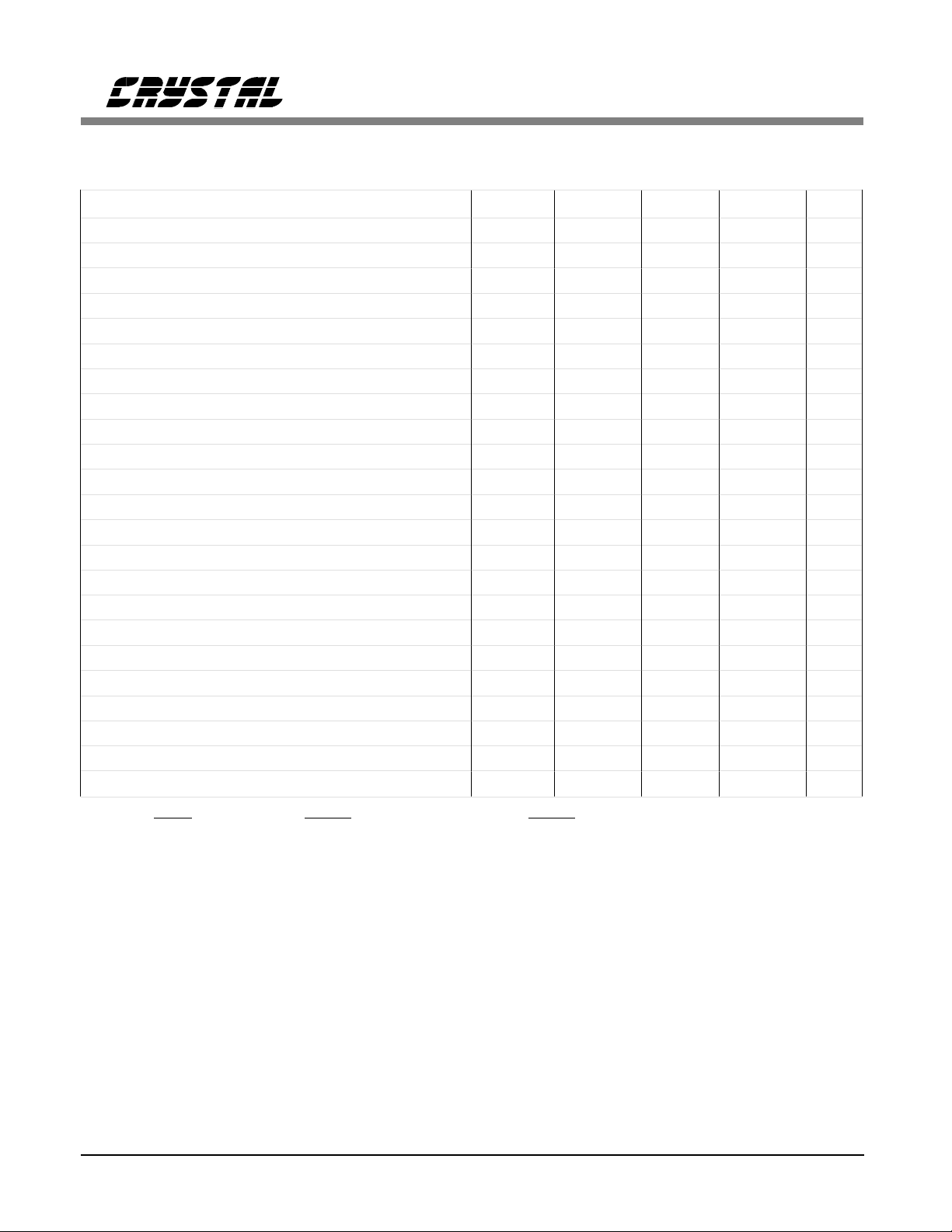
ANALOG CHARACTERISTICS (T
Fs = 48 kHz; MCLK = 12.288 MHz; SCLK = 3.072 MHz; Measurement Bandwidth is 10 Hz to 20 kHz unless otherwise specified; Logic 0 = 0V, Logic 1 = VD+)
Parameter Symbol
Temperature Range T
= 25°C; VA+ = 5V; -1 dBFS Input Sinewave, 997 Hz;
A
5330A/31A-KS
Min Typ Max
A -10 to +70 -40 to +85 °C
5330A/31A-BS
Min Typ Max Units
Dynamic Performance
Dynamic Range A-weighted 88 94 -
86 92 -
Total Harmonic Distortion+Nois e (Note 1)
-1dB
-20dB
-60dB
Total Harmonic Distortion -1dB THD - 0.003 0.02 - 0.003 0.02 %
Interchannel Phase Deviation - 0 - - 0 - Degree
Interchannel Isolation (dc to 20 kHz) - 90 - - 90 - dB
THD+N
- -84 75
- -72 66
- -32 26
86 94 84 92 -
- -84 75
- -72 66
- -32 26
dB
dB
dB
dB
dB
dc Accuracy
Interchannel Gain Mismatch - 0.1 - - 0.1 - dB
Gain Error
Gain Drift - 150 - - 150 Offset Error (Note 2) - - 0 - - 0 LSB
--±10 - - ±10
%
ppm/°C
Analog Input
Full Scale Input Voltage Range VIN 3.6 4.0 4.4 3.6 4.0 4.4 Vpp
Input Impedance (Fs = 48 kHz) ZIN - 100 - - 100 Input Bias Voltage - 2.4 - - 2.4 - V
kΩ
Power Supplies
Power Supply Current (Note 3)
VA+
Power down
Power Dissipation (Note 3)
Normal
Power Down
Power Supply Rejection Ratio PSRR - 50 - - 50 - dB
* Refer to Parameter Definitio ns at the end of th is data sheet.
Notes:1.Referenced to typical full-scale input voltage (4.0 Vpp)
2.Internal highpass filter removes offset.
3.For max power calculations, VD = 5.25 V.
IA+
-3042
- 100 1000
- 150 220
- 0.5 5.25
-3042
- 100 1000
- 150 220
- 0.5 5.25
mA
µA
mW
mW
2 DS138F2
DIGITAL CHARACTERISTICS
(T
= 25 °C; VA+ = 5V ± 5%)
A
Parameter Symbol Min Typ Max Units
CS5330A/CS5331A
High-Level Input Voltage V
Low-Level Input Voltage V
High-Level Output Voltage at lo = -20 µA
Low-Level Output Voltage at lo = 20 µA
Input Leakage Current I
IH 2.4 - - V
IL --0.8V
V
OH (VD+)-1.0 - - V
OL --0.4V
V
in --
±10.0 µA
DIGITAL FILTER CHARACTERISTICS
(T
= 25 °C; VA+ = 5V ± 5%; Fs = 48 kHz)
A
Parameter Symbol Min Typ Max Units
Passband (0.05 dB) (Note 4) 0.02 - 21.7 kHz
Passband Ripple - -
±0.05
Stopband (Note 4) 29 - 6115 kHz
Stopband Attenuation (Note 5) 80 - - dB
Group Delay (Note 6) t
Group Delay Variation vs. Frequency
gd - 15/Fs - s
∆t
gd
--0
High Pass Filter Characteristics
Frequency Response: -3 dB (Note 4)
-0.1 dB
-
-
3.7
20
-
Phase Deviation @ 20 Hz (Note 4) - 10 - Degree
Passband Ripple - - 0 dB
Notes:4.Filter characteristics scale with output sa mple rate.
5.The analog modulator samples the input at 6.144 MHz for an output sample rate of 48 kHz. There is
no rejection of input signals which are multiples of the sampling frequency ( n x 6.144 MHz ±21.7kHz
where n = 0,1,2,3...).
6.Group delay for Fs = 48kHz, t
= 15/48kHz = 312µs
gd
dB
µs
Hz
Hz
DS138F2 3
CS5330A/CS5331A
ABSOLUTE MAXIMUM RATINGS (AGND = 0V, all voltages with respect to ground.)
Parameter Symbol Min Typ Max Units
DC Power Supply: VA+ -0.3 - +6.0 V
Input Current, Any Pin Except Supplies (Note 7) Iin - Analog Input Voltage (Note 8) V
Digital Input Voltage (Note 8) V
Ambient Temperature (power applied) T
Storage Temperature T
INA -0.7 - (VA+)+0.7 V
IND -0.7 - (VA+)+0.7 V
A -55 - +125
stg -65 - +150
Notes:7.Any Pin except s upplies. Trans ient currents of up to +/- 100 mA on the analog in put pins will n ot
cause SCR latch-up.
8.The maximum over/under voltage is limited by the input current.
WARNING:Operation at or beyond these limits may result in permanent damage to the device.
Normal operation is not guaranteed at these extremes.
±10
mA
°C
°C
RECOMMENDED OPERATING CONDITIONS
(AGND = 0V; all voltages with respect to ground)
Parameter Symbol Min Typ Max Units
DC Power Supplies: VA+ 4.75 5.0 5.25 V
Analog Input Voltage (Note 9) V
Analog Input Bias Voltage 2.2 2.4 2.6 V
Note: 9.The output codes will clip at full scale with in put signals > Full Scale and < VA+.
IN -4-Vpp
Specifications are subject to change without notice.
4 DS138F2
CS5330A/CS5331A
SWITCHING CHARACTERISTICS (T
1 = VA+; C
= 20 pF) Switching characteristics are guaranteed by characterization.
L
= 25 °C; VA+ = 5V ± 5%; Inputs: Logic 0 = 0V, Logic
A
Parameter Symbol Min Typ Max Units
Output Sample Rate Fs 2 - 50 kHz
MCLK Period MCLK / LRCK = 256 t
MCLK Low MCLK / LRCK = 256 t
MCLK High MCLK / LRCK = 256 t
MCLK Period MCLK / LRCK = 384 t
MCLK Low MCLK / LRCK = 384 t
MCLK High MCLK / LRCK = 384 t
MCLK Period MCLK / LRCK = 512 t
MCLK Low MCLK / LRCK = 512 t
MCLK High MCLK / LRCK = 512 t
clkw
clkl
clkh
clkw
clkl
clkh
clkw
clkl
clkh
78 1000 ns
31 - 1000 ns
31 - 1000 ns
52 1000 ns
20 - 1000 ns
20 - 1000 ns
39 1000 ns
13 - 1000 ns
13 - 1000 ns
MASTER MODE
SCLK falling to LRCK t
SCLK falling to SDATA valid t
mslr
sdo
-10 - 10 ns
-10 - 35 ns
SCLK Duty cycle - 50 - %
SLAVE MODE
LRCK duty cycle 25 50 75 %
SCLK Period t
SCLK Pulse Width Low t
SCLK Pulse Width High t
SCLK falling to SDATA valid t
LRCK edge to MSB valid t
SCLK rising to LRCK edge delay t
sclkw
sclkl
sclkh
dss
lrdss
slr1
(Note 10) - - ns
(Note 11) - - ns
20 - - ns
- - (Note 12) ns
- - (Note 12) ns
20 - - ns
LRCK edge to rising SCLK setup time t slr2 (Note 12) - - ns
Notes: 10.
1
64 F
s
11.
1
−15 ns 12.
128 F
s
1
256 F
+ 5 ns
s
DS138F2 5
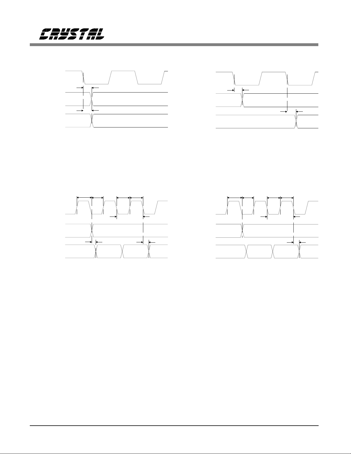
CS5330A/CS5331A
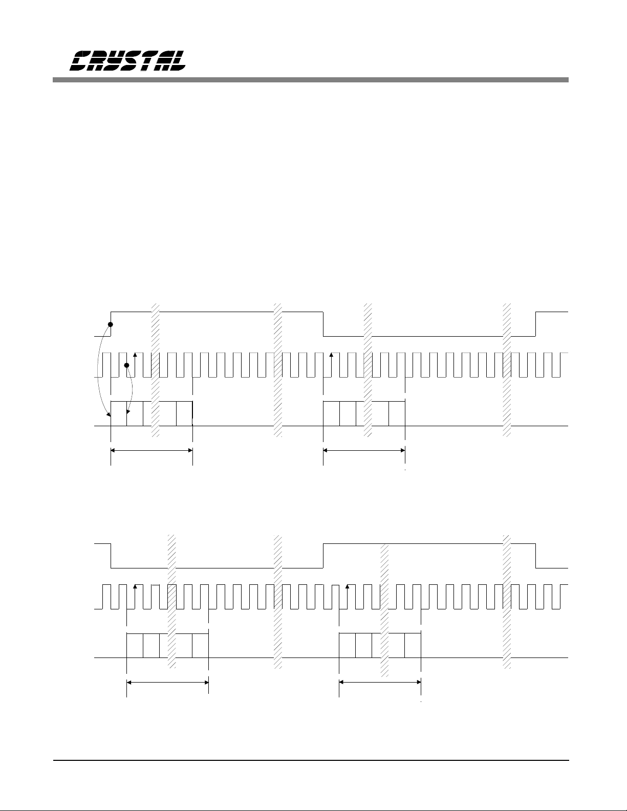
SCLK output
t
mslr
LRCK output
t
sdo
SDATA
SCLK to SDATA LRCK - MASTER mode (CS53 30A)
SCLK input
(SLAVE mode)
LRCK input
(SLAVE mode)
SDATA
t
slr1tslr2
t
lrdss
MSB MSB-1 MSB-2
t
sclkl
t
sclkh
t
sclkw
t
dss
SCLK output
t
mslr
LRCK output
t
sdo
SDATA
SCLK to SDATA LRCK - MASTER mode (CS5331A)
SCLK input
(SLAVE mode)
LRCK input
(SLAVE mode)
SDATA
t
slr1tslr2
t
sclkl
t
sclkh
t
sclkw
t
MSB MSB-1
dss
SCLK to LRCK & SDATA - SLAVE mode (CS5 330A)
SCLK to LRCK & SDATA - SLAVE mode (CS5331A)
6 DS138F2
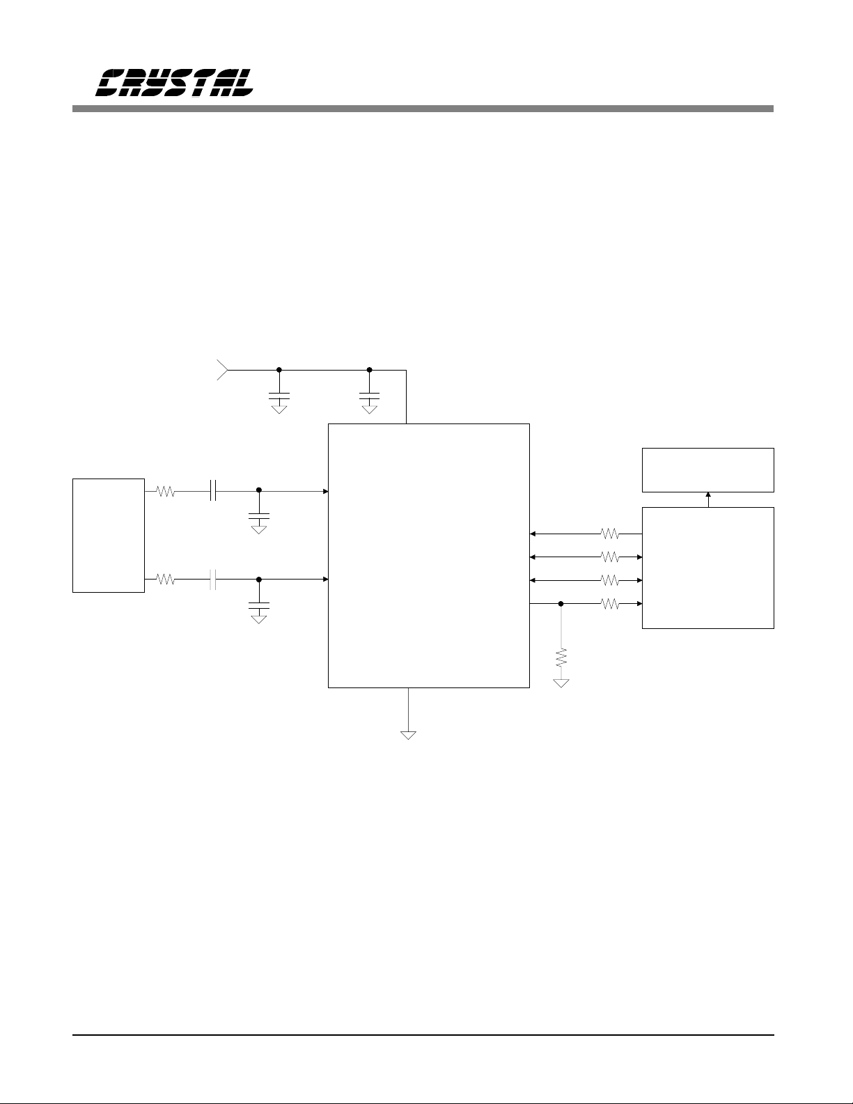
Analog
Input
Circuits
150
150
+5V
Analog
Ω
Ω
.47 µF
**
.47 µF
**
10 µF
+
.01 µF
.01 µF
0.1 µF
8
AINL
5
AINR
7
VA+
CS5330A
CS5331A
MCLK
SCLK
LRCK
SDATA
CS5330A/CS5331A
Audio Data
Processor
Ω
1 k
4
Ω
1 k
2
Ω
1 k
3
Ω
1 k
1
Timing
Logic
&
Clock
Ω
47 k
*
* Required for Master mode only
** Optional if analog input circuits biased
to within ± 5% of CS5330A/CS5331A
nominal input bias voltage
AGND
6
Figure 1. Typical Connection Diagram
DS138F2 7
CS5330A/CS5331A
GENERAL DESCRIPTION
The CS5330A and CS5331A are 18-bit, 2-channel Analog-to-Digital Converters designed for
digital audio applications. Each device uses two
one-bit delta-sigma modulators which simultaneously sample the analog input signals at 128
times the output sample rate (Fs). The resulting
serial bit streams are digitally filtered, yielding
pairs of 18-bit values. This technique yields
nearly ideal conversion perfor mance independent
of input frequency and amplitude. The converters
do not require difficult-to-design or expensive
anti-alias filters and do not require exter nal sample-and-hold amplifiers or a voltage reference.
The CS5330A and CS5331A differ only in the
output serial data format. These formats are discussed in the following sections and shown in
Figures 2 and 3.
An on-chip voltage reference provides for a single-ended input signal range of 4.0 Vpp. Output
data is available in serial form, coded as 2’s
complement 18-bit numbers. Typical power consumption is 150 mW which can be further
reduced to 0.5 mW using the Power-Down
mode.
For more information on delta-sigma modulation, see the references at the end of this data
sheet.
SYSTEM DESIGN
master clock frequencies. The output sample rate
is equal to the frequency of the Left / Right
Clock (LRCK). The serial nature of the output
data results in the left and right data words bein g
read at different times. However, the words
within an LRCK cycle represent simultaneously
sampled analog inputs. The serial clock (SCLK)
shifts the digitized audio data from the internal
data registers via the SDATA pin.
Serial Data Interface
LRCK
(kHz)
32 8.1920 12.2880 16.3840
44.1 11.2896 16.9344 22.5792
48 12.2880 18.4320 24.5760
Table 1. Common Clock Frequencies
256× 384× 512×
MCLK (MHz)
The CS5330A and CS5331A can be operated in
either Master mode, where SCLK and LRCK are
outputs, or SLAVE mode, where SCLK and
LRCK are inputs.
Master Mode
In Master mode, SCLK and LRCK are outputs
which are internally derived from MCLK. The
CS5330A/31A will divide MCLK by 4 to gener-
ate a SCLK which is 64× Fs and by 256 to
generate LRCK. The CS5330A and CS5331A
can be placed in the Master mode with a
47 kohm pull-down resistor on the SDATA pin
as shown in Figure 1.
Very few external components are required to
support the ADC. Normal power supply decoupling components and a resistor and capacitor on
each input for anti-aliasing are all that’s required,
as shown in Figure 1.
Slave Mode
LRCK and SCLK become inputs in SLAVE
mode. LRCK must be externally derived from
MCLK and be equal to Fs. The frequency of
SCLK should be equal to 64× LRCK, though
Master Clock
other frequencies are possible.
The master clock (MCLK) runs the digital filter
and is used to generate the delta-sigma modulator sampling clock. Table 1 shows some common
8 DS138F2
MCLK frequencies of 256×, 384×, and 512× Fs
are supported. The ratio of the applied MCLK to
CS5330A/CS5331A
LRCK is automatically detected during power-up
and internal dividers are set to generate the ap-
propriate internal clocks.
CS5330A
The CS5330A data output format is shown in
Figure 2. Notice that the MSB is clocked by the
transition of LRCK and the remaining seventeen
data bits are clocked by the falling edge of
SCLK. The data bits are valid during the rising
edge of SCLK.
LRCK
SCLK
01
17 17
2
18192021 22
30
CS5331A
The CS5331A data output format is shown in
Figure 3. Notice the one SCLK period delay between the LRCK transitions and the MSB of the
data. The falling edges of SCLK caus e the ADC
to output the eighteen data bits. The data bits are
valid during the rising edge of SCLK. LRCK is
also inverted compared to the CS5330A interface. The CS5331A interface is compatible with
2
I
S.
31 0 1
2
18
192021 2223
31 0 1
SDATA
LRCK
SCLK
SDATA
17 16
Left Audio Data Right Audio Data
01
17 16
Left Audio Data Right Audio Data
10
Figure 2. Data Output Timing - CS5330A
3
2
1819202122 31
10
30
01
1716
2
1716
10
3
18
1920212223
10
31 0 1
Figure 3. Data Output Timing - CS5331A (I2S compatible)
DS138F2 9

CS5330A/CS5331A
Analog Connections
Figure 1 shows the analog input connections.
The analog inputs are presented to the modulators via the AINR and AINL pins. Each analog
input will accept a maximum of 4 Vpp centered
at +2.4 V.
The CS5330A/31A samples the analog inputs at
128× Fs, 6.144 MHz for a 48 kHz sample-rate.
The digital filter rejects all noise above 29 kHz
except for frequencies right around 6.144 MHz ±
21.7 kHz (and multiples of 6.144 MHz). Most
audio signals do not have significant energy at
6.144 MHz. Nevertheless, a 150 Ω resistor in se-
ries with each analog input and a 10 nF
capacitor across the inputs will attenuate any
noise energy at 6.144 MHz, in addition to providing the optimum source impedance for the
modulators. The use of capacitors which have a
large voltage coefficient must be avoided since
these will degrade signal linearity. It is also important that the self-resonant frequency of the
capacitor be well above the modulator sampling
frequency. General purpose ceramics and film
capacitors do not meet these r equirements. However, NPO and COG capacitors are acceptable. If
active circuitry precedes the ADC, it is recommended that the above RC filter is placed
between the active circuitry and the AINR and
AINL pins. The above example frequencies scale
linearly with Fs.
This filter response scales linearly with sample
rate.
Frequency response:-3 dB @ 3.7 Hz
-0.1 dB @ 20 Hz
Phase deviation:10 degrees @ 20 Hz
Passband ripple:None
Initialization and Power-Down
The Initialization and Power-Down sequence is
shown in Figure 4. Upon initial power-up, the
digital filters and delta-sigma modulators are reset and the internal voltage reference is powered
down. The device will remain in the Initial
Power-Down mode until MCLK is presented.
Once MCLK is available, the CS5330A/31A will
make a master/slave mode decision based upon
the presence/absence of a 47 kohm pull-down resistor on SDATA as shown in Figure 1. The
master/slave decision is made during initial
power-up as shown in Figure 4.
In master mode, SCLK and LRCK are outputs
where the MCLK / LRCK frequency ratio is
256×. LRCK will appear as an output 127
MCLK cycles into the initialization sequence. At
this time, power is applied to the internal voltage
reference and the analog inputs will move to approximately 2.4 Volts. SDATA is static low
during the initialization and high pass filter settling sequence, which requires 11,265 LRCK
cycles (235 ms at a 48 kHz output sample rate).
High Pass Filter
The operational amplifiers in the input circuitry
driving the CS5330A/31A may generate a small
DC offset into the A/D converter. The
CS5330A/31A includes a high pass filter after
the decimator to remove any DC offset which
could result in recording a DC level, possibly
yielding "clicks" when switching between devices in a multichannel system.
In slave mode, SCLK and LRCK are inputs
where the MCLK / LRCK frequency ratio must
be either 256×, 384× or 512×. Once the MCLK
and LRCK are detected, MCLK occurrences are
counted over one LRCK period to determine the
MCLK / LRCK frequency ratio. At this time,
power is applied to the internal voltage reference
and the analog inputs will move to approximately 2.4 Volts. SDATA is static high during the
initialization and high pass filter settling seThe characteristics of this first-order high pass
filter are outlined below for Fs equal 48 kHz.
10 DS138F2
quence, which requires 11,265 LRCK cycles
(235 ms at a 48 kHz sample rate).

CS5330A/CS5331A
Figure 4. CS5330A/31A Initialization and Power-Down Sequence
The CS5330A and CS5331A have a PowerDown mode wherein typical consumption drops
to 0.5 mW. This is initiated when a loss of clock
is detected on either the LRCK or MCLK pins in
Slave Mode, or the MCLK pin in Master Mode.
The initialization sequence will begin when
MCLK, and LRCK for slave mode, are restored.
In slave mode power-down, the CS5330A and
CS5331A will adapt to changes in
MCLK/LRCK frequency ratio during the initiatilization sequence. It is recommended that
clocks not be applied to the device prior to
power supply settling. A reset circuit may be implemented by gating the MCLK signal.
Grounding and Power Supply Decoupling
As with any high resolution converter, the ADC
requires careful attention to power supply and
grounding arrangements if its potential perform-
ance is to be realized. Figure 1 shows the
recommended power arrangements with VA+
connected to a clean +5V supply. Decoupling
capacitors should be as near to the ADC as pos-
sible, with the low value ceramic capacitor being
the nearest. To minimize digital noise, connect
the ADC digital outputs only to CMOS inputs.
The printed circuit board layout should have
separate analog and digital regions and ground
planes. An evaluation board, CDB5330A or
CDB5331A, is available which demonstrates the
optimum layout and power supply arrangements,
as well as allowing fast evaluation of the
CS5330A and CS5331A.
DS138F2 11
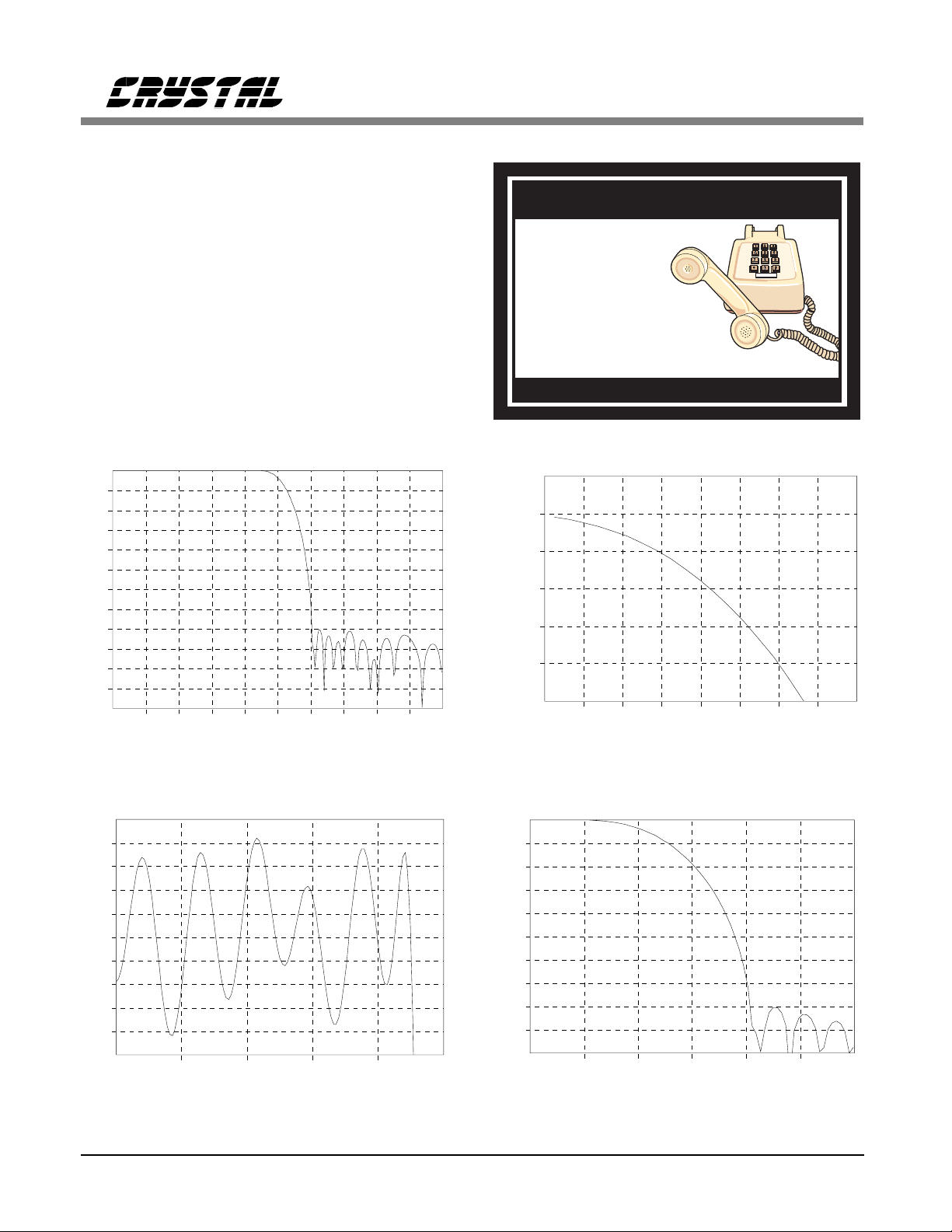
Digital Filter
Figures 5 through 8 show the attenuation characteristics of the digital filter included in the ADC.
The filter response scales linearly with sample
rate. The x-axis has been normalized to Fs, and
can be scaled by multiplying the x-axis by the
system sample rate, i.e. 48kHz.
CS5330A/CS5331A
Schematic & Layout Review Service
Confirm Optimum
Confirm Optimum
Schematic & Layout
Schematic & Layout
Before Building Your Board.
Before Building Your Board.
For Our Free Review Service
For Our Free Review Service
Call Applications Engineering.
Call Applications Engineering.
Call:(512)445-7222
0
-10
-20
-30
-40
-50
-60
-70
-80
-90
-100
-110
-120
0.0 0.1 0.2 0.3 0.4 0.5 0.6 0.7 0.8 0.9 1.0
Normalized Input Frequency
Figure 5. CS5330A/31A Digital Filter Stopband Rejection
0.05
0.04
0.03
0.02
0.01
0.00
-0.01
-0.02
-0.03
-0.04
-0.05
0
0.1 0.2 0.3 0.4 0.5
Normalized Input Frequency
2
0
-2
-4
-6
Magnitude (dB)
-8
-10
.46 .47 .48 .49 .50 .51 .52 .53 .54
Normalized Input Frequency
Figure 6. CS5330A/31A Digital Filter Transition Band
0.0
-10.0
-20.0
-30.0
-40.0
-50.0
-60.0
-70.0
-80.0
-90.0
-100.0
0.40 0.45 0.50 0.55 0.60 0.65 0.70
Normalized Input Frequency
Figure 7. CS5330A/31A Digital Filter Passband Ripple
Figure 8. CS5330A/31A Digital Filter Transition Band
12 DS138F2

PIN DESCRIPTIONS
CS5330A/CS5331A
SERIAL DATA OUTPUT SDATA AINL LEFT ANALOG INPUT
SERIAL DATA CLOCK SCLK VA+ ANALOG POWER
LEFT/RIGHT CLOCK LRCK AGND ANALOG GROUND
MASTER CLOCK MCLK AINR RIGHT ANALOG INPUT
Power Supply Connections
VA+ - Positive Analog Power, PIN 7.
Positive analog supply (Nominally +5V).
AGND - Analog Ground, PIN 6.
Analog ground reference.
Analog Inputs
AINL - Analog Left Channel Input, PIN 8.
Analog input for the left channel. Typically 4Vpp for a full-s cale input signal.
AINR - Analog Right Channel Input, PIN 5.
Analog input for the right channel. Typically 4Vpp for a full-scale input signal.
81
72
63
54
Digital Inputs
MCLK - Master Clock Input, PIN 4.
Source for the delta-sigma modulator sampling and digital filter clock. Sample rates and digital
filter characteristics scale to the MCLK frequency.
Digital Inputs or Outputs
SCLK - Serial Data Clock, PIN 2.
SCLK is an input clock at any frequency from 32× tο 64× the output word rate. SCLK can
also be an output clock at 64× if in the Master Mode. Data is clocked out on the falling edge
of SCLK.
LRCK - Left/Right Clock, PIN 3.
LRCK selects the left or right channel for output on SDATA. The LRCK frequency must be at
the output sample rate. LRCK is an output clock if in Master Mode. Although the outputs of
each channel are transmitted at different times, the two words in an LRCK cycle represent
simultaneously sampled analog inputs.
Digital Outputs
SDATA - Audio Serial Data Output, PIN 1.
Two’s complement MSB-first serial data is output on this pin. A 47 kohm resistor on this pin
will place the CS5330A/31A into Master Mode.
DS138F2 13

PARAMETER DEFINITIONS
CS5330A/CS5331A
Resolution - The total number of possible output codes is equal to 2
N
, where N = the number of bits
in the output word for each channel.
Dynamic Range - The ratio of the full scale rms value of the signal to the rms sum of all other
spectral components over the specified bandwidth. Dynamic range is a signal-to-noise
measurement over the specified bandwidth made with a -60 dBFS signal. 60 dB is then added
to the resulting measurem ent to refer the measurement to full scale. This technique ensures that
the distortion components are below the noise level and do not effect the measurement. This
measurement technique has been accepted by the Audio Engineering Society, AES17-1991, and
the Electronic Industries Association of Japan, EI AJ CP-307.
Total Harmonic Distortion+Noise (THD+N) - The ratio of the rms value of the signal to the rms sum
of all other spectral components over the specified band width (typically 10 Hz to 20 kHz),
including distortion components. Expressed in decibels. Measured at -1 and -20 dBFS as
suggested in AES17-1991 Annex A.
Total Harmonic Distortion - The ratio of the rms sum of all harmonics up to 20 kHz to the rms value
of the signal.
Interchannel Phase Deviation - The phase difference between the left and right channel sampling
times.
Interchannel Isolation - A measure of crosstalk between the left and right channels. Measured for
each channel at the converter’s output with the input under test AC grounded and a full-scale
signal applied to the other channel. Units in decibels.
Interchannel Gain Mismatch - The gain difference between left and right channels. Units in decibels.
Gain Error - The deviation of the measured full scale amplitude from the ideal full scale amplitude
value.
Gain Drift - The change in gain value with temperature. Units in ppm/°C.
Bipolar Offset Error - The deviation of the mid-scale transition (111...111 to 000...000) from the
ideal. Units in LSBs.
14 DS138F2

CS5330A/CS5331A
REFERENCES
1) " Area Efficient Decimation Filter for an 18-Bit Delta- Sigma ADC" by K. Lin and J.J. Paulos . Paper presented at the 98th Convention of the Audio Engineering Society, Febuary 1995.
2) " An 18-Bit, 8-Pin Stereo Digital-to-Analog Converter" by J.J. Paulos, A.W. Krone, G.D. Kamath
and S.T. Dupuie. Paper presented at the 97th Convention of the Audio Engineering Society, November 1994.
3) " An 18-Bit Dual-Channel Oversampling Delta-Sigma A/D Converter, with 19-Bit Mono Application Example" by Clif Sanchez. Paper presented at the 87th Convention of the Audio Engineering
Society, October 1989.
4) " The Effects of Sampling Clock Jitter on Nyquist Sampling Analog-to-Digital Converters, and on
Oversampling Delta Sigma ADC’s" by Steven Harris. Paper presented at the 87th Convention of the
Audio Engineering Society, October 1989.
5) "A Stereo 16-bit Delta-Sigma A/D Converter for Digital Audio" by D.R. Welland, B.P. Del Signore, E.J. Swanson, T. Tanaka, K. Hamas hita, S. Hara, K. Takasuka. Paper presented at the 85th
Convention of the Audio Engineering Society, November 1988.
PACKAGE DESCRIPTIONS
A
B
E
C
D
F
8-Pin
SOIC
H
J
MILLIMETERS
DIM
A
B
C
D
E
F
G
G
I
H
I
J
MIN MAX MAXMIN
TYP1.27 0.050 TYP
0.33 0.51 0.020
5.18 5.4 0.204 0.213
7.67
8.1
INCHES
0.203 0.2105.15 5.35
0 0.0100 0.25
0.070 0.0741.77 1.88
0.013
0.006 0.0100.15 0.25
8080
0.0300.0190.48 0.76
0.3190.302
Note: The EIAJ Package is not a standard JEDEC package s ize.
DS138F2 15

• Notes •
CS5330A/CS5331A
16 DS138F2

CDB5330A
CDB5331A
Evaluation Board for CS5330A / CS5331A
Features
Demonstrates recommended layout
•
and grounding arrangements
CS8402A Generates AES/EBU, S/PDIF,
•
& EIAJ-340 Compatible Digital Audio
Buffered Serial Output Interface
•
Digital and Analog Patch Areas
•
On-board or externally supplied system
•
timing
General Description
The CDB5330A/31A evaluation board is an excellent
means for quickly evaluating the CS5330A/31A 18-bit,
stereo A/D converter. Evaluation requires a digital
signal processor, a low distortion analog signal
source and a power supply. Analog inputs are provided via RCA connectors for both channels.
Also included is a CS8402A digital audio interface
transmitter which generates AES/EBU, S/PDIF, and
EIAJ-340 compatible audio data. The digital audio data
is available via RCA phono, and optical connectors.
The evaluation board may also be configured to accept
external timing signals for operation in a user application during system development.
ORDERING INFORMATION: CDB5330A, CDB5331A
Analog
Filter
Cirrus Logic, Inc.
Crystal Se micond ucto r Prod uct Divisi on
P.O. Box 17847, Austin, TX 78760
(512) 445-7222 FAX: (512) 445-7581
http://www.crystal.com
CS5330A/31A
I/OforClocks
andData
Copyri ght Cirrus Logic, Inc. 1997
CS8402A
Digital
Audio
Interface
(All Rights Reserved)
Digital
Audio
Output
OCT ’97
DS138DB2
17

CDB5330A / CDB5331A
CDB5330A/31A System Overview
The CDB5330A/31A evaluation board is an excellent means of quickly evaluating the
CS5330A/31A. The CS8402A digital audio interface transmitter provides an easy interface to
digital audio signal processors, including the majority of digital audio test equipment. The
evaluation board has been designed to accept an
analog input, and provide a digital output that is
either optical or coax. The evaluation board also
allows the user to supply clocks and data
through a 10-pin header for system development.
The CDB5330A/31A schematic has been partitioned into 5 schematics shown in Figures 2
through 6. Each partitioned schematic is represented in the system diagram shown in Figure 1.
Notice that the the system diagram also includes
the interconnections between the partitioned
schematics.
CS5330A/31A Analog to Digital Converter
A description of the CS5330A/31A is included
in the CS5330A/31A data sheet.
CS8402A Data Format
The CS8402A data format can be set with jumpers M0, M1, and M2. These formats are shown
in the CS8402A datasheet found in the 1994
Crystal Semiconductor Audio Data Book. The
format selected must be compatible with the corresponding data format of the CS5330A/31A
shown in Figures 2 and 3 of the CS5330A/31A
datasheet. The default settings for M0-M2 on the
evaluation board are given in Tables 2 and 3.
The compatible data formats for the CS8402A
and CS5330A/31A are:
CS8402A format 1;CS5330A
CS8402A format 4;CS5331A
Analog input buffer
The recommended input filter required for the
CS5330A/31A has been combined with a unity
gain input buffer (see Figure 2). The analog input filter uses a Motorola MC33202 single
supply, dual op-amp.
Power Supply Circuitry
CS8402A Digital Audio Interface
Power is supplied to the evaluation board by two
Figure 4 shows the CS8402A circuitry which
implements AES/EBU, S/PDIF and EIAJ CP340 digital audio interface standards. The
CS8402A circuit is hardware configured for consumer mode. SW2 provides 8 DIP switches to
binding posts (GND, +5V), Figure 6. The +5V
input supplies power to the +5 Volt digital circuitry (VD+), and the +5V analog circuitry
(VA+). The analog supply is derived from the
+5V binding post through a ferrite bead.
select various modes and bits for the CS8402A,
Tables 4-5. See the CS8401A/CS8402A data
Input/Output for Clocks and Data
sheet for detailed information on the operation of
the CS8402A and the digital audio standards.
The operation of the CS8402A and a discussion
of the digital audio interface are included in the
1994 Crystal Semiconductor Audio Data Book.
The evaluation board has been designed to allow
the interface to external systems via the 10-pin
CLOCK I/O header, HDR2. This header allows
the evaluation board to accept externally generated clocks. The schematic for the clock/data I/O
is shown in Figure 5. The 74HC243 transceiver
functions as an I/O buffer where the MASTER/SLAVE jumper determines if the
transceiver operates as a trans mitter or receiver.
18 DS138DB2

CDB5330A / CDB5331A
The transceiver operates as a tr ansmitter with the
MASTER/SLAVE jumper in the MAST ER position. LRCK, SDATA, and SCLK from the
CS5330A/31A will be available on HDR2.
HDR22 must be in the 0 position and HDR23
must be in the 1 position for MCLK to be an
output and to avoid bus contention on MCLK.
The transceiver operates as a receiver with the
MASTER/SLAVE jumper in the SLAVE position. LRCK and SCLK on HDR2 become inputs.
However, the recommended mode of operation is
to generate MCLK on the evaluation board with
HDR23 in the 0 position and HDR22 in the 1
position. These default settings allow MCLK to
be an output, with LRCK and SCLK as inputs.
MCLK is always an output from the evaluation
board.
Grounding and Power Supply Decoupling
The CS5330A/31A requires careful attention to
power supply and grounding arrangements to optimize performance. Figure 2 shows the
recommended power arrangements. The
CS5330A/31A is positioned over the analog
ground plane, near the digital/analog ground
plane split, to minimize the distance that the
clocks travel. The series resistors are present on
the clock lines to reduce the effects of transient
currents when driving a capacitive load in master
mode, and reduce clock overshoot when applying external clocks to the CS5330A/31A in slave
mode.
This layout technique is used to minimize digital
noise and to insure proper power supply matching/sequencing. The decoupling capacitors are
located as close to the CS5330A/31A as possible. Extensive use of ground plane fill on both
the analog and digital sections of the evaluation
board yield large reductions in radiated noise effects.
CONNECTOR INPUT/OUTPUT SIGNAL PRESENT
+5V input
GND input ground connection from power supply
AINL input left channel analog input
AINR input right channel analog input
MCLK, SCLK, LRCK,
SDATA
Digital Output output digital audio interface output via coax
Optical Output output digital audio interface output via optical
DS138DB2 19
input/output I/O for master, serial, left/righ t clocks, and serial DATA
Table 1. System Connections
(VD+) for CS8402A and digital section
(VA+) for CS5330A/31A and Analog input filter op-amp

CDB5330A / CDB5331A
JUMPER PURPOSE POSITION FUNCTION SELECTED
HDR1
HDR10
HDR9
HDR22
HDR23
HDR6
HDR5 (M2)
HDR4 (M1) *Low
HDR3 (M0) *High
* Default setting from factory
CS5330A/31A SCLK
Selection for CS8402A
Master/Slave Mode
Selection
Selects source of system
clocks
Clock I/O
Selects 256× or
512× MCLK for CS8402A
CS8402A mode select
Table 2. CDB5330A Jumper Selectable Options
*5330A CS5330A Selected
5331A CS5331A Selected
*High
Low
*High MASTER Mode (5330A Clocks)
Low SLAVE Mode (External Clocks)
*0
*1
*256
512
*Low
MASTER Mode
SLAVE Mode
Input/Output for Clocks and Data
See
section of text
See CS8402A data sheet for details
See CS8402A data sheet
for details
JUMPER PURPOSE POSITION FUNCTION SELECTED
HDR1
HDR10
HDR9
HDR22
HDR23
HDR6
HDR5 (M2)
HDR4 (M1) *Low
HDR3 (M0) *Low
* Default setting from factory
CS5330A/31A SCLK
Selection for CS8402A
Master/Slave Mode
Selection
Selects source of system
clocks
Clock I/O
Selects 256× or
512× MCLK for CS8402A
CS8402A mode select
Table 3. CDB5331A Jumper Selectable Options
5330A CS5330A Selected
*5331A CS5331A Selected
*High
Low
*High MASTER Mode (5331A Clocks)
Low SLAVE Mode (External Clocks)
*0
*1
*256
512
*High
MASTER Mode
SLAVE Mode
Input/Output for Clocks and Data
See
section of text
See CS8402A data sheet for details
See CS8402A data sheet
for details
20 DS138DB2

Switch# 0=Closed, 1=Open Comment
3
1,4 FC1, FC0 C24,C25,C26,C27 - Sample Frequency
2
5
6
8,7
* Default setting from factory
PRO=0 Consumer Mode C0=0
0 0
*0 1
1 0
1 1
C3 C3,C4,C5 - Emphasis (1 of 3 bits)
*1
0
C2 C2 - Copy/Copyright
1
*0
C15 C15 - Generation Status
1
*0
C8, C9 C8-C14 - Category Co de (2 of 7 b its)
1 1
1 0
0 1
*0 0
0000 - 44.1 kHz
0100 - 48 kHz
1100 - 32 kHz
0000 - 44.1 kHz, CD Mode
000 - None
100 - 50/15 µs
0 - Copy Inhibited/Copyright Asserted
1 - Copy Permitted/Copyright No t Asserted
0 - Definition is based on category code.
1 - See CS8402A Data Sheet, App. A
0000000 - General
0100000 - PCM encoder/decoder
1000000 - Compact Disk - CD
1100000 - Digital Audio Tape - DAT
CDB5330A / CDB5331A
Table 4. CS8402A Switch Definitions - Consumer Mode
Switch# 0=Closed, 1=Open Comment
3
1 CRE Local Sample Address Coun ter & Reliability Fla gs
default
2,5
default
4
default
6
default
8,7 EM1, EM0 C2,C3,C4 - Emphasis (2 of 3 bits)
default
PRO=0 Professional Mode C0=1(default)
0
1
C6, C7 C6,C7 - Sample Frequency
1 1
1 0
0 1
0 0
C1 C1 - Audio
1
0
C9 C8,C9,C10,C11 - Channel Mode (1 of 4 bits)
1
0
1 1
1 0
0 1
0 0
Disabled
Internally Generated
00 - Not Indicated - Default to 48 kHz
01 - 48 kHz
10 - 44.1 kHz
11 - 32 kHz
0 - Normal Audio
1 - Non-Audio
0000 - Not indicated - Default to 2-channel
0100 - Stereophonic
000 - Not Indicated - default to none
100 - No emphasis
110 - 50/15 µs
111 - CCITT J.17
Table 5. CS8402A Switch Definitions - Professional Mode
DS138DB2 21

CDB5330A / CDB5331A
Figure 1. System Block Diagram and Signal Flow
22 DS138DB2

DS138DB2 23
Figure 2. CS5330A/31A and Connections
CDB5330A / CDB5331A

CDB5330A / CDB5331A
Figure 3. MCLK Generation and Power Down
24 DS138DB2

DS138DB2 25
Figure 4. CS8402A Digital Audio Transmitter Connections
Optional Toshi ba P art T OTX123 avail able thro ugh In sigh t El ectro nics
Schott Corp. Transformer Part 121960-602 available through Schott Corp., Wayzata, MN.
CDB5330A / CDB5331A

CDB5330A / CDB5331A
Figure 5. I/O Interface for Clocks and D ata
Figure 6. Power Supply
26 DS138DB2

CDB5330A / CDB5331A
Figure 7. CDB5330A/31A Component Side Silkscreen
DS138DB2 27
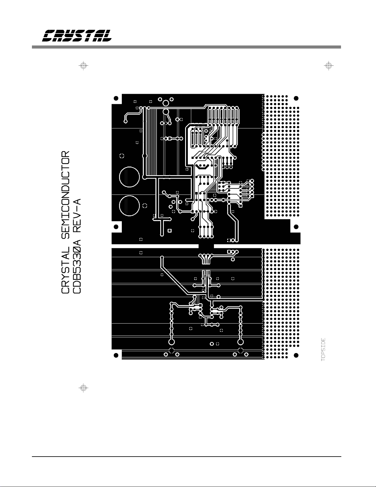
CDB5330A / CDB5331A
Figure 8. CDB5330A/31A Component Side (top)
28 DS138DB2

CDB5330A / CDB5331A
Figure 9. CDB5330A/31A Solder Side (bottom)
DS138DB2 29

 Loading...