

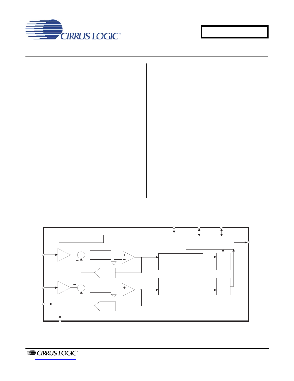
High
Pass
Filter
AINR
S/H
AGND
AINL
S/H
DAC
Serial Output Interface
Voltage Reference
Comparator
Comparator
LP Filter
LP Filter
VA+
SCLK
Digital Decimation
Filter
SDATA
MCLK
DAC
High
Pass
Filter
LRCK
8
5
6
423
1
7
Digital Decimation
Filter
CS5330A/31A
8-Pin, Stereo A/D Converter for Digital Audio
Features
Single +5 V Power Supply
18-Bit Resolution
94 dB Dynamic Range
Linear Phase Digital Anti-Alias Filtering
– 0.05 dB Passband Ripple
– 80 dB Stopband Rejection
Low Power Dissipation: 150 mW
– Power-Down Mode for Portable
Applications
Complete CMOS Stereo A/D System
– Delta-Sigma A/D Converters
– Digital Anti-Alias Filtering
– S/H Circuitry and Voltage Reference
Adjustable System Sampling Rates including
32, 44.1, and 48 kHz
General Description
The CS5330A/31A is a complete stereo ana log-to- digital converter that performs antialias filtering, sampling
and analog-to-digital conversion generating 18-bit values for both left and right inputs in serial form. The
output sample rate can be infinitely adjusted between
2 kHz and 50 kHz.
The CS5330A/31A operates from a single +5 V supply
and requires only 150 mW for no rmal operation, making
it ideal for battery-powered applications.
The ADC uses delta-sigma modulation with 128X oversampling, followed by digital filtering and decimation,
which removes the need for an external anti-alias filter.
The linear-phase digital filter has a passband to
21.7 kHz, 0.05 dB passband ripple and >80 dB stopband rejection. The device also contains a high-pass filter to remove DC offsets.
The device is available in an 8-pin SOIC package in
both Commercial (
(-40° to +85° C)
page 16 for complete details.
-10° to +70° C) and Automotive grades
. Please refer to “Ordering Information” on
http://www.cirrus.com
Copyright Cirrus Logic, Inc. 2011
(All Rights Reserved)
MAY '11
DS138F6

TABLE OF CONTENTS
1. PIN DESCRIPTIONS .................................... .... ... ... ... .... .......................................... ... ... ... ........ 3
2. CHARACTERISTICS AND SPECIFICATIONS ........................................................................ 4
SPECIFIED OPERATING CONDITIONS................................................................................. 4
ABSOLUTE MAXIMUM RATINGS........................................................................................... 4
ANALOG INPUT CHARACTERISTICS.................................................................................... 5
DIGITAL CHARACTERISTICS............................... ... .... ... ... ... .... ... ... ... ... .... ... ... ... .... ... .............. 6
DIGITAL FILTER CHARACTERISTICS ........................................................ ... ... .... ... ... ........... 6
SWITCHING CHARACTERISTICS........................... .... ... .......................................... ... ... ... .... . 7
3. GENERAL DESCRIPTION ............................................................... ... ... .... ... ... ... .... ... ... ........... 9
3.1 System Design .................................................................................................................. 9
3.1.1 Master Clock ......................................................................................................... 9
3.1.2 Serial Data Interface ............................................................................................ 9
3.1.3 Master Mode ......................................................................................................... 9
3.1.4 Slave Mode ......................................................................................................... 10
3.1.5 CS5330A ............................................................................................................. 10
3.1.6 CS5331A ............................................................................................................. 10
3.1.7 Analog Connections ............................................................................................ 11
3.1.8 High-Pass Filter .................................................................................................. 11
3.1.9 Initialization and Power-Down ............................................................................. 11
3.1.10 Grounding and Power Supply Decoupling ..................... ................................... 12
3.1.11 Digital Filter ....... ... ... .... .......................................... ... ... ... ... .... ... ... ... .... ............... 13
4. PARAMETER DEFINITIONS .................................................................................................. 14
5. REFERENCES ........................................................................................................................ 15
6. PACKAGE DESCRIPTIONS .................................................................................................. 15
7. ORDERING INFORMATION . ... ... .... ... ... .......................................... ... ... .... ... ... ... .... ... ... ... ... ... 16
8. REVISION HISTORY .............................................................................................................. 16
CS5330A/31A
LIST OF FIGURES
Figure 1. Typical Connection Diagram......................................................................................... 8
Figure 2. Data Output Timing-CS5330A.............................. ... ... .... ... ... ... ... .... ... ... ... .... ... ... ... ... ... 10
Figure 3. Data Output Timing - CS5331A (I²S Compatible)....................................................... 10
Figure 4. CS5330A/31A Initialization and Power-Down Sequence............ .... ... ... ... .... ... ... ... ... ... 12
Figure 5. CS5330A/31A Digital Filter Stopband Rejection......................... .... ... ... ... .... ... ... ... ... ... 13
Figure 6. CS5330A/31A Digital Filter Transition Band............................................................... 13
Figure 7. CS5330A/31A Digital Filter Passband Ripple............................................................. 13
Figure 8. CS5330A/31A Digital Filter Transition Band............................................................... 13
LIST OF TABLES
Table 1. Common Clock Frequencies......................................................................................... 9
2 DS138F6
1. PIN DESCRIPTIONS
S
T
CS5330A/31A
Pin Name
SDATA
SCLK
LRCK
MCLK
AINR
AGND
VA+
AINL
ERIAL DATA OUTPUT
SERIAL DATA CLOCK
LEFT/RIGHT CLOCK
MASTER CLOCK
#
Pin Description
Audio Serial Data Output (Output) - Two’s complement MSB-first serial data is output on this
1
pin. A 47 k resistor on this pin will place the CS5330A/31A into Master Mode.
Serial Data Clock (Input/Output) - SCLK is an input clock at any fr equency from 32 x to 64x the
2
output word rate. SCLK can also be an output clock at 64x if in the Master Mode. Data is
clocked out on the falling edge of SCLK.
Left/Right Clock (Input/Output) - LRCK selects the lef t or right channel for output on SDATA.
The LRCK frequency must be at the output sample rate. LRCK is an output clock if in Master
3
Mode. Although the outputs of each channel are transmitted at dif feren t times, the two words in
an LRCK cycle represent simultaneously sampled analog inputs.
Master Clock Input (Input) - Source for the delta-sigma modulator sampling and digital filter
4
clock. Sample rates and digi tal filter characteristics scale to the MCLK frequency.
Analog Right Channel Input (Input) - Analog input for the right channel. Typically 4 Vpp for a
5
full-scale input signal.
6
Analog Ground (Input) - Analog ground reference.
7
Positive Analog Power (Input) - Positive analog supply (Nominally +5 V).
Analog Left Channel Input (Input) - Analog input for the left channel. Typically 4 Vpp for a full-
8
scale input signal.
SDATA
SCLK
LRCK
MCLK
81
AINL
72
VA+
63
AGND
54
AINR
LEFT ANALOG INPUT
ANALOG POWER
ANALOG GROUND
RIGHT ANALOG INPU
DS138F6 3
CS5330A/31A
2. CHARACTERISTICS AND SPECIFICATIONS
(All Min/Max characteristics and specifications are guaranteed over the Specified Operating Conditions. Typical
performance characteristics and spe cif icat ion s ar e de riv e d from measurements taken at nominal supply voltages
and T
= 25C.)
A
SPECIFIED OPERATING CONDITIONS
(AGND = 0V, all voltages with respect to ground)
Parameter Symbol Min Typ Max Unit
Analog Supply Voltage
Ambient Operating Temperature (Power Applied) KSZ
BSZ, DSZ
VA+ 4.75 5.0 5.25 V
T
A
-10
-40
-
+70
-
+85
°C
°C
ABSOLUTE MAXIMUM RATINGS
(AGND = 0V, all voltages with respect to ground.) (Note 1)
Parameter Symbol Min Typ Max Unit
Analog Supply Voltage
Input Current, Any Pin Except Supplies (Note 2)
Analog Input Voltage (Note 3)
Digital Input Voltage (Note 3)
Ambient Temperature (power applied)
Storag e Temperature
VA+ -0.3 - +6.0 V
lin - - ±10 mA
INA -0.7 - VA+0.7 V
V
IND -0.7 - VA+0.7 V
V
TA -55 - +125 °C
Tstg -65 - +150 °C
Notes:
1. Operation at or beyond the se limits may result in permanent damage to the device. Normal operation
is not guaranteed at these extremes.
2. Any pin except supplies. Transient current of up to +/- 100 mA on the analog input pins will not cause
SCR latch-up.
3. The maximum over/under voltage is limited by the input current.
4 DS138F6
CS5330A/31A
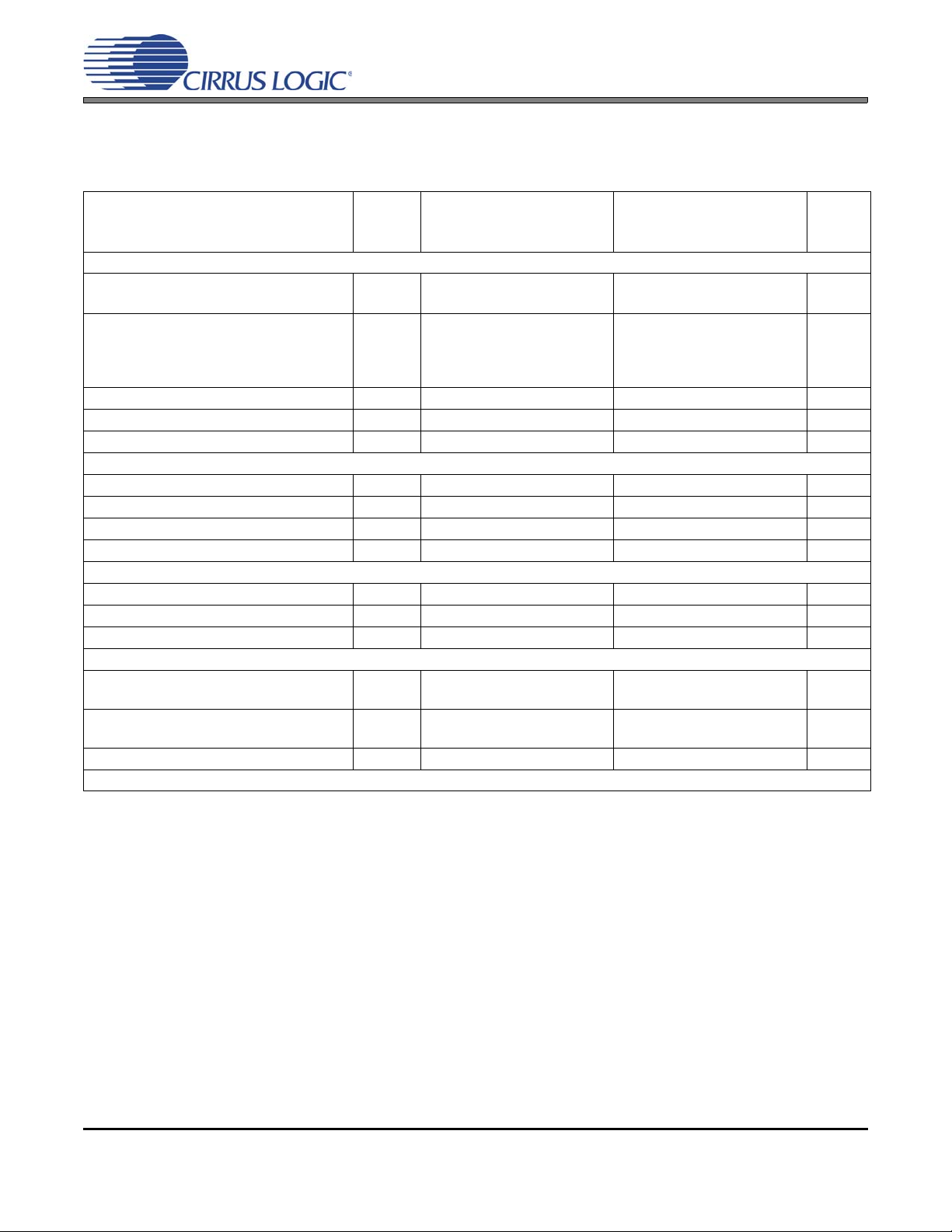
ANALOG INPUT CHARACTERISTICS
(-1 dBFS input sine wave, 997 Hz; Measurement Bandwidth is 10 Hz to 20 kHz unless otherwise specified; Logic
0 = 0V, Logic 1 = VD+)
CS5330A-BSZ
CS5330A/31A-KSZ
Parameter Symbol
Min Typ Max
Dynamic Performance
Dynamic Range
A-weighted
unweighted
88
86
Total Harmonic Distortion + Noise
(Note 4)
-1 dB
-20 dB
-60 dB
Total Harmonic Distortion -1 dB
Interchannel Phase Deviation
Interchannel Isolation (DC to 20 kHz)
THD+N
THD - 0.003 0.02 - 0.003 0.2 %
-
-
-
-0--0-Degree
-90--90-dB
DC Accuracy
Interchannel Gain Mismatch
Gain Error
Gain Drift
Offset Error (Note 5)
- 0.1 - - 0.1 - dB
--±10--±10%
- 150 - - 150 - ppm/°C
--0--0LSB
Analog Input
Full-scale Input Voltage
Input Impedance (Fs = 48 kHz)
Input Bias Voltage
VIN 3.6 4.0 4.4 3.6 4.0 4.4 Vpp
ZIN - 100 - - 100 - k
2.2 2.4 2.6 2.2 2.4 2.6 V
Power Supplies
Power Supply Current VA+
Power down
Power Dissipation Normal
Power down
Power Supply Rejection Ratio
IA+ -
-
-
-
PSRR - 50 - - 50 - dB
* Refer to Parameter Definitions at the end of this data sheet.
94
92
-84
-72
-32
30
100
150
0.5
-
-
75
66
26
42
1000
220
5.25
CS5331A-DSZ
Min Typ Max Unit
86
84
-
-
-
94
92
-84
-72
-32
75
66
26
-
-
dB
dB
dB
dB
dB
-
-
-
-
30
100
150
0.5
42
1000
220
5.25
mA
µA
mW
mW
4. Referenced to typical full-scale input voltage.
5. Internal highpass filter removes offset.
DS138F6 5
DIGITAL CHARACTERISTICS
Parameter Symbol Min Typ Max Unit
High-Level Input Voltage
Low-Level Input Voltage
High-Level Output Voltage at lo = -20 µA
Low-Level Output Voltage at lo = 20 µA
Input leakage Current
DIGITAL FILTER CHARACTERISTICS
(FS = 48 kHz)
Parameter Symbol Min Typ Max Unit
Passband
Passband Ripple
Stopband (Note 6)
Stopba nd Attenuation (Note 7)
Group Delay (Note 8)
Group Delay Variation vs. Frequency
High Pass Filter Characteristics
Frequency Response:
Phase Deviation @ 20 Hz (Note 6)
Passband Ripple
(0.05) (Note 6)
-3 dB (Note 6)
-0.1 dB
CS5330A/31A
VIH 2.4 - - V
VIL --0.8V
VOH VA-1.0 - - V
VOL --0.4V
Iin - - ±10.0 µA
0.02 - 21.7 kHz
--±0.05dB
29 - 6115 kHz
80 - - dB
gd -15/Fs-s
t
tgd --0µs
-
-
- 10 - Degree
--0dB
3.7
20
-
-
Hz
Hz
6. Filter characteristics scale with output sample rate.
7. The analog modulator samples the input at 6.144 MHz for an output sa mple rate of 48 kHz. The re is no
rejection of input signals which are multiples of the sampling frequency (n x 6.144 MHz ±21.7 kHz where
n = 0,1,2,3…).
8. Group delay for Fs = 48 kHz, t
gd = 15/48 kHz = 312 µs.
6 DS138F6

CS5330A/31A
1
64 F
s
1
128 F
s
- 15 ns
1
256 F
s
+ 5 ns
SWITCHING CHARACTERISTICS
(Inputs: Logic 0 = 0V, Logic 1 = VA+; CL = 20 pF) Switching ch aracteristics ar e guaran teed by characterization .
Parameter Symbol Min Typ Max Unit
Output Sample Rate
MCLK Period MCLK/LRCK = 256
MCLK Low MCLK/LRCK = 256
MCLK High MCLK/LRCK = 256
MCLK Period MCLK/LRCK = 384
MCLK Low MCLK/LRCK = 384
MCLK High MCLK/LRCK = 384
MCLK Period MCLK/LRCK = 512
MCLK Low MCLK/LRCK = 512
MCLK High MCLK/LRCK = 512
MASTER MODE
SCLK falling to LRCK
SCLK falling to SDATA valid
SCLK Duty cycle
SLAVE MODE
LRCK duty cycle
SCLK Period
SCLK Pulse Width Low
SCLK Pulse Width High
SCLK falling to SDATA valid
LRCK edge to MSB valid
SCLK rising to LRCK edge delay
LRCK edge to rising SCLK setup time
Fs 2 - 50 kHz
t
clkw 78 - 1000 ns
t
clkl 31 - 1000 ns
t
clkh 31 - 1000 ns
t
clkw 52 - 1000 ns
t
clkl 20 - 1000 ns
t
clkh 20 - 1000 ns
t
clkw 39 - 1000 ns
t
clkl 13 - 1000 ns
t
clkh 13 - 1000 ns
t
mslr -10 - 10 ns
t
sdo -10 - 35 ns
-50-%
25 50 75 %
t
clkw (Note 9) --ns
t
clkl (No te 10) --ns
t
clkh 20 - - ns
t
dss - - (Note 11) ns
t
lrdss - - (Note 11) ns
t
slr1 20 - - ns
t
slr2 (Note 11) --ns
9.
10.
11.
DS138F6 7

SCLK output
SDATA
t
sdo
LRCK output
t
msl
r
SCLK to SDATA LRCK - MASTER mode (CS53 30A)
SCLK output
t
mslr
SDATA
t
sdo
LRCK output
SCLK to SDATA LRCK - MASTER mode (CS5331A)
(
(
s
1
SCLK to LRCK & SDATA - SLAVE mode (CS5331A)
(
(
s
2
SCLK to LRCK & SDATA - SLAVE mode (CS5330A)
+5V
Figure 1. Typical Connection Diagram
CS5330A/31A
SCLK input
SLAVE mode)
LRCK input
SLAVE mode)
SDATA
Analog
Input
Circuits
150
150
Analog
Ω
Ω
t
slr1tslr2
.47 μF
**
.47 μF
**
t
t
sclkh
sclkl
t
lrdss
MSB MSB-1 MSB-
10 μF
+
0.1 μF
8
AINL
.01 μF
5
AI
NR
.01 μF
t
sclkw
t
ds
VA+
CS5330A
CS533
SCLK input
SLAVE mode)
LRCK input
SLAVE mode)
7
1A
SDATA
MCLK
SCL
LRCK
SDATA
t
slr1tslr2
t
sclkl
t
sclkh
t
sclkw
MSB MSB-
t
ds
Audio Data
Processor
Ω
1 k
4
K
3
1
1 k
1 k
Ω
Ω
Ω
1 k
2
Timing
Logic
&
Clock
Required for Master mode only
*
Optional if analog input circuits biased
**
to within ± 5% of CS5330A/CS5331A
nominal input bias voltage
8 DS138F6
Ω
47 k
*
AGND
6
CS5330A/31A
3. GENERAL DESCRIPTION
The CS5330A and CS5331A are 18-bit, 2-channel Analog-to-Digital Converters designed for digital audio applications. Each device uses two one-bit delta-sigma modulators which simultaneously sample the analog input signals
at 128 times the output sample rate (Fs). The resulting serial bit streams are digitally filt ered, yielding pair s of 18-bit
values. This technique yields nearly ideal conversion performance independent of input frequency and amplitude.
The converters do not require difficult-to-design or expensive anti-alias filters and do not require external sampleand-hold amplifiers or a voltage reference.
The CS5330A and CS5331A differ only in the o utput serial data format. These formats are discussed in the following
sections and shown in Figures 2 and 3.
An on-chip voltage reference provides for a single-ended input signal range of 4.0 Vpp. Output data is available in
serial form, coded as 2’s complement 18-bit numbers. Typical power consumption is 150 mW which can be further
reduced to 0.5 mW using the Power-Down mode.
For more information on delta-sigma modulation, see the references at the end of this data sheet.
3.1 System Design
Very few external components are required to support the ADC. Normal power supply decoupling components and a resistor and capacitor on each input for anti-aliasing are all that are required, as shown in
Figure 1.
3.1.1 Master Clock
The master clock (MCLK) runs the digital filter and is used to generate the delta-sigma modulator sampling clock. Table 1 shows some common master clock frequencies. The output sample rate is equal to
the frequency of the Left / Right Clock (LRCK). The serial nature of the output data results in the left and
right data words being read at different times. However, the words within an LR CK cycle represent simultaneously sampled analog inputs. The serial clock (SCLK) shifts th e digitized audio data from the internal
data registers via the SDATA pin.
3.1.2 Serial Data Interface
LRCK
(kHz)
32 8.1920 12.2880 16.3840
44 11.2896 16.9344 22.5792
48 12.2880 18.4320 24.5760
The CS5330A and CS5331A can be operated in either Master mode, where SCLK and LRCK ar e outputs,
or SLAVE mode, where SCLK and LRCK are inputs.
3.1.3 Master Mode
In Master mode, SCLK and LRCK are outputs which are internally derived from MCLK. The CS5330A/31A
will divide MCLK by 4 to generate a SCLK which is 64Fs and by 256 to generate LRCK. The CS5330A
and CS5331A can be plac ed in the Master m ode with a 47-k pull-down resistor on the SDATA pin as
shown in Figure 1.
MCLK (MHz)
256x 384x 512x
Table 1. Common Clock Frequencies
DS138F6 9

3.1.4 Slave Mode
01
2
18 19 20 21 22
31 0 1
2
18
19 20 21 22 23
31 0 1
SCLK
LRCK
Left Audio Data Right Audio Data
17 16
10
17 16
10
SDATA
17 17
30
Figure 2. Data Output Timing-CS5330A
01
2
18 19 20 21 22 31
01
2
18
19 20 21 22 23
31 0 1
SCLK
LRCK
Left Audio Data Right Audio Data
17 16
10
17 16
10
SDATA
3
3
30
Figure 3. Data Output Timing - CS5331A (I²S Compatible)
LRCK and SCLK become inputs in SLAVE mode. LRCK must be externally derived from MCLK and be
equal to Fs. The frequency of SCLK should be equal to 64xLRCK, though other frequencies are possible.
MCLK frequencies of 256x, 384x, and 512xFs are supported. The ratio of the applied MCLK to LRCK is
automatically detected during power-up and internal dividers are set to generate the appropriate internal
clocks.
3.1.5 CS5330A
The CS5330A data output format is shown in Figure 2. Notice that the MSB is clocked by the transition of
LRCK and the remaining seventeen data bits are clocked by the falling edge of SCLK. The data bits are
valid during the rising edge of SCLK.
3.1.6 CS5331A
The CS5331A data output format is shown in Figure 3. Notice the one SCLK period delay between the
LRCK transitions and the MSB of the data. The falling edges of SCLK cause the ADC to output the eighteen data bits. The data bits are valid during the ri sing edge of SCLK. L RCK is also inverte d compared to
the CS5330A interface. The CS5331A interface is compatible with I
CS5330A/31A
2
S.
10 DS138F6

3.1.7 Analog Connections
Figure 1 shows the analog input connections. The analog inputs are presented to the modulators via the
AINR and AINL pins. Each analog input will accept a maximum of 4 Vpp centered at +2.4 V.
The CS5330A/31A samples the analog inputs at 128 Fs, 6.144 MHz for a 48 kHz sample-rate. The dig-
ital filter rejects all noise above 29 kHz except for frequencies right around 6.144 MHz 21.7 kHz (and
multiples of 6.144 MHz). Most audio signals do not have significant energy at 6.144 MHz. Nevertheless,
a 150 resistor in series with each analog input and a 10 nF capacitor across the inputs will attenuate
any noise energy at 6.144 MHz, in addition to providing the optimum source impedance for the modulators. The use of capacitors which have a large voltage coefficient must be avoided since these will degrade signal linearity. It is also important that the self-resonant frequency of the capacitor be well above
the modulator sampling frequency. General purpose ceramics and film capacitors do not meet these requirements. However, NPO and COG capacitors are acceptable. If active circuitry precedes the ADC, it
is recommended that the above RC filter is placed between the active circuitry and the AINR and AINL
pins. The above example frequencies scale linearly with Fs.
3.1.8 High-Pass Filter
The operational amplifiers in the input circuitry driving the CS5330A/31A may generate a small DC offset
into the A/D converter. The CS533 0A/31A includes a high pass filter after the decimator to remove any
DC offset which could result in recording a DC level, possibly yielding "clicks" when switching between
devices in a multichannel system.
CS5330A/31A
The characteristics of this first-order high pass filter are outlined in the “Digital Filter Characteristics” on
page 6
3.1.9 Initialization and Power-Down
The Initialization and Power-Down sequence is shown in Figure 4. Upon initial power-up, the digital filters
and delta-sigma modulators are reset and the internal voltage reference is powered down. The device will
remain in the Initial Power-Down mode until MCLK is presented. Once MCLK is available, the
CS5330A/31A will make a master/slave mode decision based upon the presence/absence of a 47-k
pull-down resistor on SDATA as shown in Figure 1. The master/slave decision is made during initial power-up as shown in Figure 4.
In master mode, SCLK and LRCK are outputs where the MCLK/LRCK frequency ratio is 256x. LRCK will
appear as an output 127 MCLK cycles into the initializati on sequence. At this time , power is applied to the
internal voltage reference and the analog inputs will move to approximately 2.4 Volts. SDATA is static low
during the initialization and high pass filter settling sequence, which requires 11,265 LRCK cycles (235
ms at a 48 kHz output sample rate).
In slave mode, SCLK and LRCK a re in pu ts whe r e t h e MCLK/LRCK frequency ratio must be either 256x,
384x,or 512x. Once the MCLK and LRCK are detected, MCLK oc currence s are co unted over on e LRCK
period to determine the MCLK/LRCK frequency ratio. At this time, power is applied to the internal voltage
reference and the analog inputs will move to approximately 2.4 Volts. SDATA is static high during the initialization and high pass filter settling sequence, which requires 11,265 LRCK cycles (235 ms at a 48 kHz
sample rate).
DS138F6 11

CS5330A/31A
Figure 4. CS5330A/31A Initialization and Power-Down Sequence
The CS5330A and CS5331A have a Power-Down mode wherein typical consumption drops to 0.5 mW.
This is initiated when a loss of clock is detected on either the LRCK or MCLK pins in Slave Mode, or the
MCLK pin in Master Mode. The initialization sequence will begin when MCLK (and LRCK for slave mode)
are restored. In slave mode power-down, the CS5330A and CS5331A will adapt to changes in
MCLK/LRCK frequency ratio during the initialization sequence. It is recommended that clocks not be applied to the device prior to power supply settling. A reset circui t may be implemented b y gating the MCLK
signal.
3.1.10 Grounding and Power Supply Decoupling
As with any high resolution converter, the ADC requires careful attention to power supply and grounding
arrangements if its potential performance is to be realized. Figure 1 shows the recommended power arrangements with VA+ connected to a clean +5-V supply. Decoupling capacitors should be as near to the
ADC as possible, with the low value ceramic capacitor being the nearest. To minimize digital noise, connect the ADC digital outputs only to CMOS inputs. The printed circuit board layout should have separate
analog and digital regions and ground planes. An evaluation board, CDB5330A or CDB5331A, is available which demonstrates the optimum layout and power supply arrangements, as well as allowing fast
evaluation of the CS5330A and CS5331A.
12 DS138F6

3.1.11 Digital Filter
0
-10
-20
-30
-40
-50
-60
-70
-80
-90
-100
-110
-120
0.0 0.1 0.2 0.3 0.4 0.5 0.6 0.7 0.8 0.9 1.0
Normalized Input Frequency
2
4
Magnitude (dB)
Figure 5. CS5330A/31A Digital Filter Stopband Rejection Figure 6. CS5330A/31A Digital Filter Transition Band
0.05
0.04
0.03
0.02
0.01
0.00
-0.01
-0.02
-0.03
-0.04
-0.05
0 0.1 0.2 0.3 0.4 0.5
Normalized Input Frequency
0.0
-
0
Figure 7. CS5330A/31A Digital Filter Passband Ripple Figure 8. CS5330A/31A Digital Filter Transition Band
Figures 5 through 8 show the attenuation char acteristics of the digital filter included in the ADC. The filter
response scales linearly with sample rate. The x-axis has been normalized to Fs and can be scaled by
multiplying the x-axis by the system sample rate, i.e. 48 kHz.
CS5330A/31A
0
-2
-4
-6
-8
-10
.46 .47 .48 .49 .50 .51 .52 .53
Normalized Input Frequency
.5
-10.0
-20.0
-30.0
-40.0
-50.0
-60.0
-70.0
-80.0
-90.0
100.0
0.40 0.45 0.50 0.60 0.65 0.7
Normalized Input Frequency
DS138F6 13

4. PARAMETER DEFINITIONS
Resolution
The total number of possible output codes is equal to 2 N, where N = the nu mber of bits in the output word
for each channel.
Dynamic Range
The ratio of the full-scale rms value of the signal to the rms sum of all other spectral components over the
specified bandwidth. Dynamic range is a signal-to-noise measurement over the specified bandwidth made
with a -60 dBFS signal. 60 dB is then added to the resulting measurement to refer the measurement to full
scale. This technique ensures that the distortion components are be low the noise level and do not effect the
measurement. This measurement technique has been accepted by the Audio Engineering Society, AES171991, and the Electronic Industries Association of Japan, EIAJ CP-307.
Total Harmonic Distortion + Noise (THD+N)
The ratio of the rms value of the signal t o the rms su m of all other spectral components over the specified
bandwidth (typically 10 Hz to 20 kHz), including distortion components. Expressed in decibels. Measured
at -1 and -20 dBFS as suggested in AES17-1991 Annex A.
Total Harmonic Distortion
The ratio of the rms sum of all harmonics up to 20 kHz to the rms value of the signal.
CS5330A/31A
Interchannel Phase Deviation
The phase difference between the left and right channel sampling times.
Interchannel Isolation
A measure of crosstalk between the left and right channels. Measured for each channel at the converter’s
output with the input under test AC grounded and a full-scale signal applied to the other channel. Units in
decibels.
Interchannel Gain Mismatch
The gain difference between left and right channels. Units in decibels.
Gain Error
The deviation of the measured full-scale amplitude from the ideal full-scale amplitude value.
Gain Drift
The change in gain value with temperature. Units in ppm/°C.
Bipolar Offset Error
The deviation of the mid-scale transition (111...111 to 000...000) from the ideal. Units in LSBs.
14 DS138F6

CS5330A/31A
8-Pin
SOIC
F
G
J
I
H
B
A
E
D
C
5. REFERENCES
1. Area Efficient Decimation Filter for an 18-Bit Delta- Sigma ADC, by K. L in and J. J. Paulos. Paper presented
at the 98th Convention of the Audio Engineering Society, February 1995.
2. An 18-Bit, 8-Pin Stereo Digital-to-Analog Converter, by J. J. Paulos, A. W. Krone, G. D. Kamath and S. T.
Dupuie. Paper presented at the 97th Convention of the Audio Engineering Society, November 1994.
3. An 18-Bit Dual-Channel Oversampling Delta-Sigma A/D Converter, with 19-Bit Mono Application Example,
by Clif Sanchez. Paper presented at the 87th Convention of the Audio Engineering Society, October 1989.
4. The Effects of Sampling Clock Jitter on Nyquist Sampling Analog-to-Digital Converters, and on Oversam-
pling Delta Sigma ADC’s, by Steven Harris. Paper presented at the 87th Conven tion of the Audio Engineering Society, October 1989.
5. A Stereo 16-bit Delta-Sigma A/D Converter for Digital Audio, by D. R. Welland, B. P. Del Signore, E. J.
Swanson, T. Tanaka, K. Hamashita, S. Hara, K. Takasuka. Paper presented at the 85th Convention of the
Audio Engineering Society, November 1988.
6. PACKAGE DESCRIPTIONS
Millimeters Inches
DIM MIN MAX MIN MAX
A 5.15 5.35 0.203 0.210
B 1.27 TYP 0.050 TYP
C 0 0.25 0 0.010
D 1.77 1.88 0.070 0.074
E 0.33 0.51 0.013 0.020
DS138F6 15
Note: The EIAJ Package is not a standard JEDEC package size.
F .15 0.25 0.006 0.010
G0°8°0°8°
H 5.18 5.4 0.204 0.213
I 0.48 0.76 0.019 0.030
J 7.67 8.1 0.302 0.319
CS5330A/31A
Contacting Cirrus Logic Support
For all product questions and inquiries, contact a Cirrus Logic Sales Representative.
To find the one nearest to you, go to www.cirrus.com.
IMPORTANT NOTICE
Cirrus Logic, Inc. and its subsidiaries ("Cirrus") believe that the information contained in this document is accurate and reliable. However, the information is subject
to change without not ice and is pr ovided "AS IS" witho ut warr anty of any kind (express or implied). Customers are advised to obtain the latest version of relevant
information to verify, before placing orders, that information being relied on is current and complete. All products are sold subject to the terms and conditions of sale
supplied at the time of order acknowledgment, including those pertaining to warranty, indemnification, and limitation of liability. No responsibility is assumed by Cirrus
for the use of this information, including use of this information as the basis for manufacture or sale of any items, or for infringement of patents or other rights of third
parties. This document is the property of Cirrus and by furnishing this information, Cirrus grants no license, express or implied under any patents, mask work rights,
copyrights, trademarks, trade secrets or other inte llectual property rig hts. Cirrus owns the copyrights associated with the information contained herein and gives consent for copies to be made of the information only for use within your organization with respect to Cirrus integrated circuits or other products of Cirrus. This consent
does not extend to other copying such as copying for general distribution, advertising or promotional purposes, or for creating any work for resale.
CERTAIN APPLICATIONS USING SEMICONDUCTOR PRODUCTS MAY INVOLVE POTENTIAL RISKS OF DEATH, PERSONAL INJURY, OR SEVERE PROPERTY OR ENVIRONMENTAL DAMAGE (“CRITICAL APPLICATIONS”). CIRRUS PRODUCTS ARE NOT DESIGNED, AUTHORIZED OR WARRANTED FOR USE
IN AIRCRAFT SYSTEMS, MILITARY APPLICATIONS, PRODUCTS SURGICALLY IMPLANTED INTO THE BODY, AUTOMOTIVE SAFETY OR SECURITY DEVICES, LIFE SUPPORT PRODUCTS OR OTHER CRITICAL APPLICATIONS. INCLUSION OF CIRRUS PRODUCTS IN SUCH APPLICATIONS IS UNDERSTOOD TO BE FULLY AT THE CUSTOMER’S RISK AND CIRRUS DISCLAIMS AND MAKES NO WARRANTY, EXPRESS, STATUTORY OR IMPLIED,
INCLUDING THE IMPLIED WARRANTIES OF MERCHANTABILITY AND FITNESS FOR PARTICULAR PURPOSE, WITH REGARD TO ANY CIRRUS PRODUCT
THAT IS USED IN SUCH A MANNER. IF THE CUSTOMER OR CUSTOMER’S CUSTOMER USES OR PERMITS THE USE OF CIRRUS PRODUCTS IN CRITICAL
APPLICATIONS, CUSTOMER AGREES, BY SUCH USE, T O FULLY INDEMNIF Y CIRRUS, ITS OF FICE RS, DI RECTORS, EMPLOYEES, DISTRI BUTORS AND
OTHER AGENTS FROM ANY AND ALL LIABILITY, INCLUDING ATTORNEYS’ FEES AND COSTS, THAT MAY RESULT FROM OR ARISE IN CONNECTION
WITH THESE USES.
Cirrus Logic, Cirrus, and the Cirrus Logic logo designs are trademarks of Cirrus Logic, Inc. All other brand and product names in this document may be trademarks
or service marks of their respective owners.
7. ORDERING INFORMATION
Product D escription Package Pb-Free Grade Temp Range Container Order #
CS5330A
CS5331A
CS5330A
CS5331A
8-pin, Stereo A/D Con-
verter for Digital Audio
8-pin, Stereo A/D Con-
verter for Digital Audio
8-pin, Stereo A/D Con-
verter for Digital Audio
8-pin, Stereo A/D Con-
verter for Digital Audio
8-SOIC YES Commercial -10° to +70° C
8-SOIC YES Commercial -10° to +70° C
8-SOIC YES Automotive -40° to +85° C
8-SOIC YES Automotive -40° to +85° C
Bulk CS5330A-KSZ
Tape & Reel CS5330A-KSZR
Bulk CS5331A-KSZ
Tape & Reel CS5331A-KSZR
Bulk CS5330A-BSZ
Tape & Reel CS5330A-BSZR
Bulk CS5331A-DSZ
Tape & Reel CS5331A-DSZR
8. REVISION HISTORY
Release Changes
F5 Updated Ordering Information
F6 • Removed CS5330A-KS, CS5330A-KSR, CS5331A-KS, CS5331A-KSR, and CS5330A-BS, and CS5330A-BSR
from the ordering information table in Section 7 as well as corresponding data in Section 2, “Charact eristics and
Specifications.”
• Added entry for BSZ and BSZR automotive products to Ordering Information.
• Added CS5330A-BSZ to heading of Analog Input Characteristics table in Section 2.
16 DS138F6
 Loading...