

CS5317
16-Bit, 20 kHz Oversampling A/D Converter
Features
l Complete Voiceband DSP Front-E nd
- 16-Bit A/D Converter
- Internal Track & Hold Amplifier
- On-Chip Voltage Reference
- Linear-Phase Digital Filter
l On-Chip PLL for Simplified Output Phase
Locking in Modem Applications
l 84 dB Dynamic Range
l 80 dB Total Harmonic Distortion
l Output Word Rates up to 20 kHz
l DSP-Compatible Serial Interface
l Low Power Dissipation: 220 mW
Description
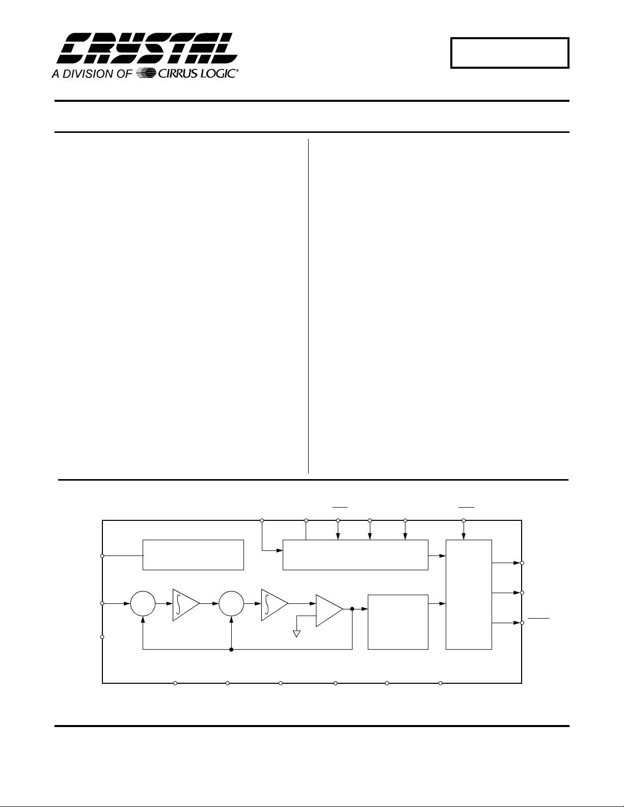
The CS5317 is an ideal anal og front-end for voice band
signal processing applications such as high-performance modems, passive sonar, and voice rec ognition
systems. It includes a 16-bit A/D converter with an internal track & hold amplifier, a voltage reference, and a
linear-phase digital filter.
An on-chip phase-l ock loop (PLL) circuit simplifies th e
CS5317’s use in applications where the output word rate
must be locked to an external sampling signal.
The CS5317 uses delta-sigma modulation to achieve
16-bit output word rates up to 20 kHz. The delta-sigm a
technique utilizes oversampli ng followed by a digital filtering and decimation process. The combination of
oversampling and d igital fi ltering gr eatly ea ses anti alias
requirements. Thus, the CS531 7 offers 84 dB dynamic
range and 80 dB THD and signal bandwidths up to
10 kHz at a fraction of t he cost of hybrid and discrete
solutions.
The CS5317’s advanced CMOS construction provides
low power consumptio n of 220 mW and the inher en t reliability of monolithic devices.
I
9ROWDJH
5HIHUHQFH
9$
9$
$,1
1&
5()%8)
Cirrus Logic, Inc.
Crystal Semiconductor Products Division
P.O. Box 17847, Austin, Texas 78760
(512) 445 7222 FAX: (512) 445 7581
http://www.crystal.com
9&2,1
ORDERING INFORMATION
See page 20.
3+'756702'(&/.,1
3//&ORFN*HQHUDWRU
&RPSDUDWRU
$*1'
Copyright Cirrus Logic, Inc. 1997
9'
(All Rights Reserved)
WK2UGHU
'HFLPDWLRQ
)LOWHU
9'
'*1'
'2(
6WDWH
%XIIHUV
&/.287
'$7$
'287
MAR ‘95
DS27F4
1
CS5317
ANALOG CHARACTERISTICS
(TA = T
MIN
- T
; VA+, VD+ = 5V ±10%; VA-, VD- = -5V ±10%;
MAX
CLKIN = 4.9152 MHz in CLKOR mode; 1kHz Input Sinewave; with 1.2 kΩ, .01 µF antialiasing filter.)
Parameter* Min Typ Max Units
Specified Temperature Range 0 to 70 °C
Resolution 16 - - Bits
Dynamic Performance
Dynamic Rnage (Note 1) 78 84 - dB
Total Harmonic Distortion 72 80 - dB
Signal to Intermodulation Distorition - 84 - dB
dc Accuracy
Differential Nonlinearity (Note2) Positive Full-Scale Error Positive Full-Scale Drift Bipolar Offset Error Bipolar Offset Drift -
±
±
±
±
±
0.4
150
500
10
50
-LSB
-mV
-
µ
V/°C
-mV
-
µ
V/°C
Filter Characteristics
Absolute Group Delay (Note 3) 78.125 - -
µ
s
Passband Frequency (Note 4) - 5 - kHz
Input Characteristics
AC Input Impedance ( 1kHz) - 80 Analog Input Full Scale Signal Level
±
2.75
--V
Ω
k
Power Supplies
Power Dissipation (Note5) - 220 300 mW
Notes: 1. Measured over the full 0 to 9.6kHz band with a -20dB input and extrapolated to full-sc ale. Since this
includes energy in the stopband above 5kHz, additional post-filtering at the CS5317’s output can
typically achieve 88dB dynamic range by improving rejection above 5kHz. This can be increased to
90dB by bandlimiting the output to 2.5kHz.
2. No missing codes is guaranteed by design.
3. Group delay is constant with respect to input analog frequency; that is, the digital FIR filter has
linear phase. Group delay is determined by the formula D
= 384/CLKIN in CLKOR mode, or
grp
192/CLKOUT in any mode.
4. The digital filter’s frequency response sc ales with the master clock . Its -3dB point is deter mined by
= CLKIN/977.3 in CLKOR mode, or CLKOUT/488.65 in any mode.
f
-3dB
5. All outputs unloaded. All inputs CMOS levels .
* Refer to the
Parameter Definitions
section after the Pin Description section.
2 DS27F4
ANALOG CHARACTERISTICS (continued)
Parameter Min Typ Max Units
CS5317
Power Supply Rejection VA+ (Note 6)
VAVD+
VD-
-
-
-
-
60
45
60
55
-
-
-
-
dB
dB
dB
dB
Specified Temperature Range 0 to 70 °C
Phase-Lock Loop Characteristics
VCO Gain Constant, Ko (Note 7) -4 -10 -30 Mrad/Vs
VCO Operating Frequency 1.28 - 5.12 MHz
Phase Detector Gain Control, Kd -3 -8 -12
µ
A/rad
Phase Detector Prop. Delay (Note 8) - 50 100 ns
Notes: 6. With 300mV p-p, 1kHz ripple applied to each supply separately.
7. Over 1.28 MHz to 5.12 MHz VCO output range, where VCO frequency = 2 * CLKOUT.
8. Delay from an input edge to the phase detector to a response at the PHDT output pin.
DIGITAL CHARACTERISTICS
(TA = T
MIN
- T
; VA+, VD+ = 5V±10%; VA-, VD- = -5V±10%)
MAX
All measurements performed under static conditions.
Parameter Symbol Min Typ Max Units
High-Level Input Voltage V
Low-Level Input Voltage V
High-Level Output Voltage (Note 9) V
Low-Level Output Voltage I
= 1.6mA V
OUT
Input Leakage Current I
3-State Leakage Current I
Digital Output Pin Capacitance C
Note: 9. I
=-100µA. This specification guarantees the ability to drive one TTL load (VOH=2.4V @ I
out
IH
IL
OH
OL
in
OZ
out
2.0 - - V
--0.8V
(VD+)-1.0V - - V
--0.4V
--10
--
±10µ
µ
-9-pF
=-40µA.).
out
A
A
RECOMMENDED OPERATING CONDITIONS (DGND, AGND = 0V, see Note 10.)
Parameter Symbol Min Typ Max Units
DC Power Supplies: Positive Digital
Negative Digital
Positive Analog
Negative Analog
Master Clock Frequency f
Note: 10. All voltages with respect to ground.
Specifications are subject to change without notice.
DS27F4 3
VD+
VD-
VA+
VA-
clk
4.5
-4.5
4.5
-4.5
5.0
-5.0
5.0
-5.0
5.5
-5.5
5.5
-5.5
V
V
V
V
0.01 - 5.12 MHz
CS5317
SWITCHING CHARACTERISTICS
(TA = T
MIN-TMAX
Parameter Symbol Min Typ Max Units
Master Clock Frequency: CLKIN
CLKG1 Mode
CLKG2 Mode
CLKOR Mode
Output Word Rate: D OUT f
Rise Times: Any Digital Input
Any Digital Output
Fall Times: Any Digital Input
Any Digital Output
CLKIN Duty Cycle
CLKG1 and CKLG2 Modes Pulse Width Low
Pulse Width High
CLKOR Mode Pulse Width Low
Pulse Width High
RST Pulse Width Low t
Set Up Times: RST High to CLKIN High
CLKIN High to RST High
Propagation Delays:
DOE Falling to Data Valid
CLKIN Rising to DOUT Falling (Note 11)
DOE Rising to Hi-Z Output
CLKOUT Rising to DOUT Falling
CLKOUT Rising to DOUT Rising
CLKOUT Rising to Data Valid
CLKIN Rising to CLKOUT Falling (Note 12)
CLKIN Rising to CLKOUT Rising (Note 12)
Notes: 11. CLKIN only pertains to CLKG1 and CLKG2 modes.
12. Only valid in CLKOR mode.
; CL=50 pF; VD+ = 5V±10%; VD- = -5V±10%)
f
clkg1
f
clkg2
f
clkor
dout
t
risein
t
riseout
t
fallin
t
fallout
t
pwl1
t
pwh1
t
pwl1
t
pwh1
pwr
t
su1
t
su2
t
phl1
t
phl2
t
plh1
t
plh2
t
plh3
t
plh4
t
plh5
t
plh6
-
-
-
--20kHz
-
-
-
-
200
200
45
45
400 - - ns
40
40
-
-
-
-
-
-
-
-
20
15
20
15
1
-
-
-
20
10
5.12
1000
20
1000
20
-
-
-
-
-
-
-
-
-
-
-
-
-
-
-
-
-
-
-
150
80
60
60
100
200
200
CLKOUT
cycles
kHz
kHz
MHz
ns
ns
ns
ns
ns
ns
ns
ns
ns
ns
ns
ns
ns
ns
ns
ns
ABSOLUTE MAXIMUM RATINGS (DGND, AGND = 0V, all voltages with repect to groung)
Parameter Symbol Min Max Units
DC Power Supplies: Positive Digital
Negative Digital
Positive Analog
Negative Analog
Input Current, Any Pin Except Supplies (Note 13) I
Analog Input Voltage (AIN and VREF pins) V
Digital Input Voltage V
Ambient Operating Temperature T
Storage Temperature T
Notes: 13. Transient currents up to 100mA will not cause SCR latch-up.
WARNING:Operating this device at or beyond thes e extremes may result in permanent damage to the device.
Normal operation of the part is not guaranteed at these extremes.
4 DS27F4
VD+
VD-
VA+
VA-
in
INA
IND
A
stg
-0.3
0.3
-0.3
0.3
-
(VA+) + 0.3
-6.0
6.0
-6.0
±10
mA
(VA-) - 0.3 (VA+) + 0.3 V
-0.3 (VD+) + 0.3 V
-55 125 °C
-65 150 °C
V
V
V
V
CS5317
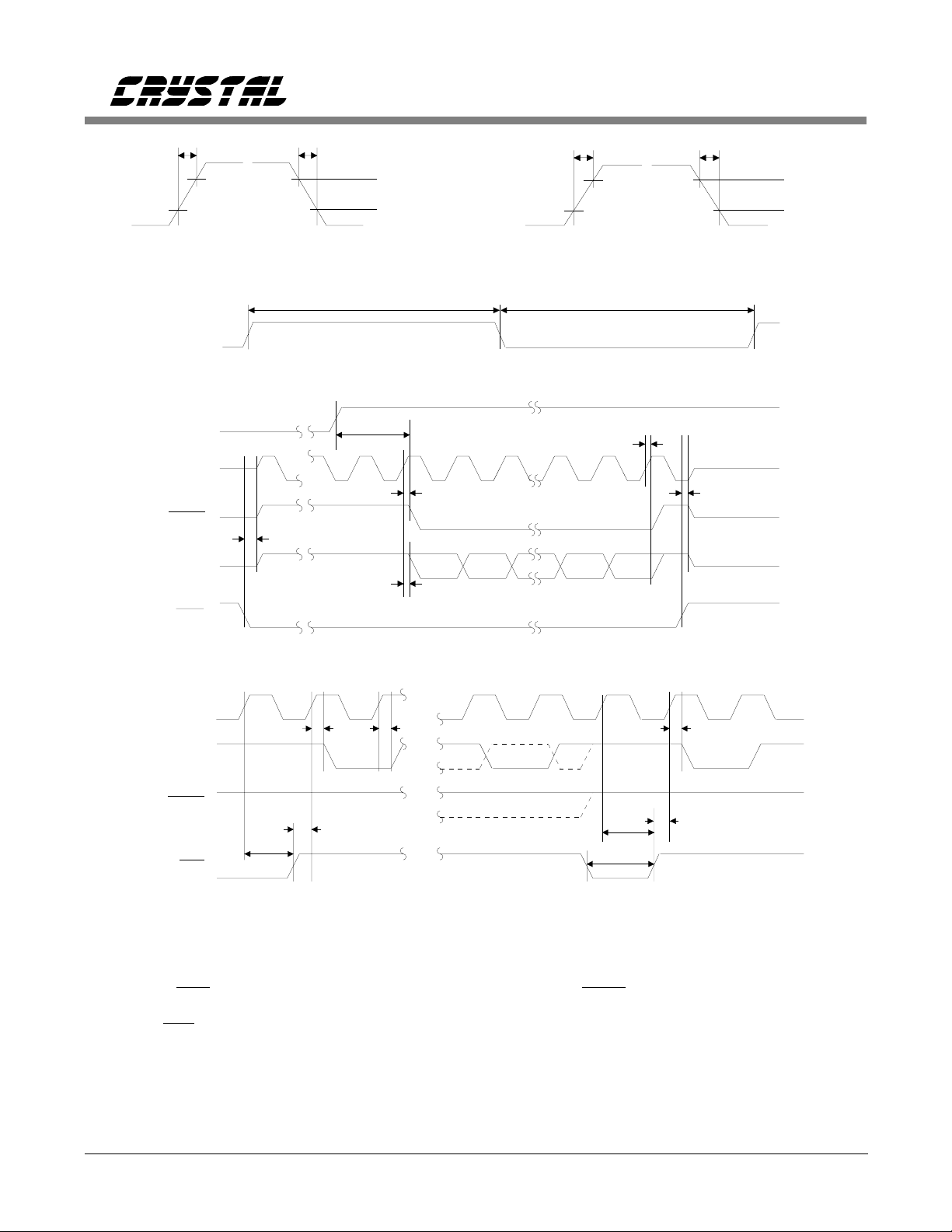
CLKIN
CLKIN
(Note 14)
CLKOUT
DOUT
DATA
t
risein
t
phl1
t
fallin
t
pwh1
t
phl2
t
plh4
2.0 V
0.8 V
Rise and Fall Times
CLKIN Timing
t
plh2
(MSB)
14
1015
t
riseout
t
pwl1
t
plh3
t
t
plh1
fallout
2.4 V
0.4 V
DOE
(Note 15)
Serial Output Timing
CLKIN
t
plh6
CLKOUT
DOUT
RST
(Note 16)
t
su2
t
plh5
t
su1
Reset Timing
Notes: 14. CLKIN only pertains to CLKG1 and CLKG2 modes.
DOE is brought high during serial data transfer, CLKOUT, DOUT, and DATA will immediately
15. If
3-state and the rest of the serial data is lost.
RST must be held high except in the clock ov erride (CLKOR) mode where it can be used to align
16.
the phases of all internal clocks.
t
su2
t
pwr
t
t
su1
plh5
DS27F4 5

CS5317
GENERAL DESCRIPTION
The CS5317 functions as a complete data conversion subsystem for voiceband signal processing.
The A/D converter, sample/hold, voltage reference, and much of the antialiasing filtering are
performed on-chip. The CS5317’s serial interface
offers its 16-bit, 2’s complement output in a format which easily interfaces with
industry-standard micro’s and DSP’s.
The CS5317 also includes a phase-locked loop
that simplifies the converter’s application in systems which require sampling to be locked to an
external signal source. The CS5317 continuously
samples its analog input at a rate set by an external clock source. On-chip digital filtering, an
integral part of the delta-sigma ADC, processes
the data and updates the 16-bit output register at
up to 20 kHz. The CS5317 can be read at any rate
up to 20 kHz.
The CS5317 is a CS5316 with an on-chip sampling clock generator. As such, it replaces the
CS5316 and should be considered for all new designs. In addition, a CS5316 look-alike mode is
included, allowing a CS5317 to be dropped into a
CS5316 socket.
modulator’s 1-bit output conveys information in
the form of duty cycle. The digital filter then
processes the 1-bit signal and extracts a high
resolution output at a much lower rate (that is,
16-bits at a 20 kHz word rate with a 5 kHz input
bandwidth).
An elementary example of a delta-sigma A/D
converter is a conventional voltage-to-frequency
converter and counter. The VFC’s 1-bit output
conveys information in the form of frequency (or
duty-cycle), which is then filtered (averaged) by
the counter for higher resolution. In comparison,
the CS5317 uses a more sophisticated multi-order
modulator and more powerful FIR filtering to extract higher word rates, much lower noise, and
more useful system-level filtering.
Filtering
At the system level, the CS5317’s digital filter
can be modeled exactly like an analog filter with
a few minor differences. First, digital filtering resides behind the A/D conversion and can thus
reject noise injected during the conversion process (i.e. power supply ripple, voltage reference
noise, or noise in the ADC itself). Analog fil tering
cannot.
Also, since digital filtering resides behind the
THEORY OF OPERATION
A/D converter, noise riding unfiltered on a near-
full-scale input could potentially saturate the
The CS5317 utilizes the delta-sigma technique of
executing low-cost, high-resolution A/D conversions. A delta-sigma A/D converter consists of
two basic blocks: an analog modulator and a digital filter.
ADC. In contrast, analog filtering removes the
noise before it ever reaches the converter. To ad-
dress this issue, the CS5317’s analog modulator
and digital filter reserve headroom such that the
device can process signals with 100mV "excur-
sions" above full-scale and still output accurately
Conversion
converted and filtered data. Filtered input signals
above full-scale still result in an output of all
The analog modulator consists of a 1-bit A/D
ones.
converter (that is, a comparator) embedded in an
analog negative feedback loop with high openloop gain. The modulator samples and converts
the analog input at a rate well above the band-
An Application Note called "Delta Sigma Over-
view" contains more details on delta-sigma
conversion and digital filtering.
width of interest (2.5 MHz for the CS5317). The
6 DS27F4
CS5317
SYSTEM DESIGN WITH THE CS5317
Like a tracking ADC, the CS5317 continuously
samples and converts, always tracking the analog
input signal and updating its output register at a
20 kHz rate. The device can be read at any rate to
create any system-level sampling rate desired up
to 20kHz.
Clocking
Oversampling is a critical function in delta-sigma
A/D conversion. Although system-level output
sample rates typically remain between 7kHz and
20kHz in voiceband applications, the CS5317 actually samples and converts the analog input at
rates up to 2.56 MHz. This internal sampling rate
is typically set by a master clock which is on the
order of several megahertz. See Table1 for a complete description of the clock relationships in the
various CS5317 operating modes.
Some systems such as echo-canceling modems,
though, require the output sampling rate to be
locked to a sampling signal which is 20 kHz or
below. For this reason the CS5317 includes an
on-chip phase-lock loop (PLL) which can gener-
ate its requisite 5.12 MHz master clock from a
20 kHz sampling signal.
The CS5317 features two modes of operation
which utilize the internal PLL. The first, termed
Clock Generation 1 (CLKG1), accepts a sam-
pling clock up to 20 kHz at the CLKIN pin and
internally generates the requisite 5.12 MHz clock.
The CS5317 then processes samples updating its
output register at the rate defined at CLKIN, typi-
cally 20 kHz. For a 20 kHz clock input the digital
filter’s 3 dB corner is set at 5.239 kHz, so CLKG1
provides a factor of 2X oversampling at the sys-
tem level (20 kHz is twice the minimum possible
sampling frequency needed to reconstruct a 5
kHz input). The CLKG1 mode is initiated by ty-
ing the MODE input to +5V.
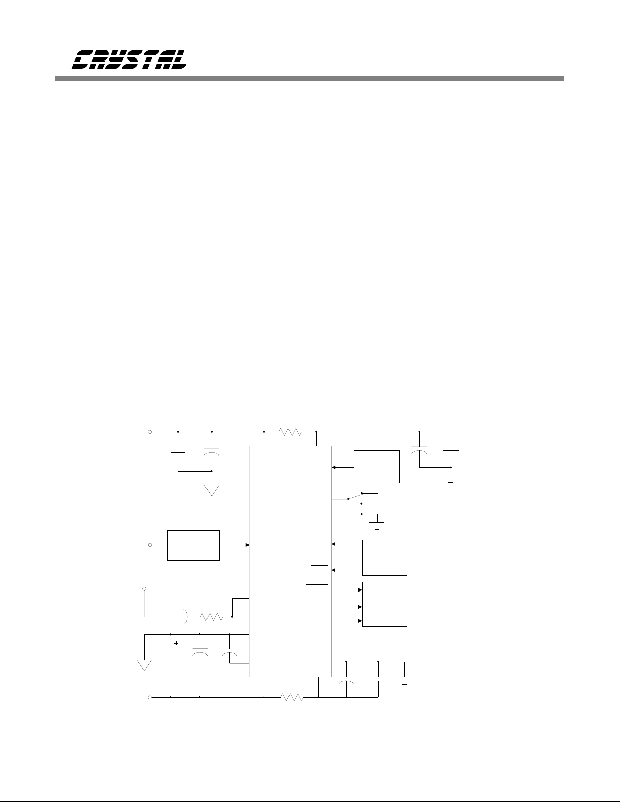
+5V
Analog
Supply
Analog
Signal
Source
VA+
-5V
Analog
Supply
10
Ω
0.1
F
µ
10
µ
10
Conditioning
25 nF
10
µ
µ
Signal
F
0.1
µ
F
F
Ω
25 k
0.1
0.1
µ
µ
F
1 2
VA+ VD+
MODE
CS5317
11
AIN
± 2.75V
10
DOUT
DATA
CLKOUT
Ω
18
17
15
F
12
VCOIN
PHDT
AGND
REFBUF
VA-
14
CLKIN
RST
DOE
DGND
VD-
10
4
0.1
9
Clock
Source
7
16
3
8
6
5
VD- (clock override mode / CLKOR)
VD+ (clock gen. mode / CLKG1)
(clock gen. mode / CLKG2)
uP or DSP
Control
Serial
Data
Interface
10
µ
µ
F
F
Figure 1. System Connection Diagram with Example PLL Components
F
DS27F4 7
CS5317
Output Word
Rate Provides
Mode
Mode Symbol
Clock
Gen. 2
Clock
Gen. 1
Clock
Override
CS5316 CS5316 FSYNC LOW YES 5120.0 (max) 2.56 20.0 20.0 N/A
* t
dcD
CLKG2
CLKG2
CLKG2
CLKG1
CLKG1
CLKG1
CLKOR
CLKOR
CLKOR
- Delay from CLKIN rising to DOUT falling = 1 CLKOUT cycle
Pin RESET
0V HIGH NO 7.2
+5V HIGH YES 14.4
-5V SYNC YES 3686.4
System-level 2X
Oversampling
Table 1. Mode Comparisons
CLKIN
(kHz)
9.6
10.0 (max)
19.2
20.0 (max)
4915.2
5120.0 (max)
CLKOUT
f
sin
(MHz)
1.8432
2.4576
2.56
1.8432
2.4576
2.56
1.8432
2.4576
2.56
DOUT
f
sout
(kHz)F(kHz)
7.2
9.6
10.0
14.4
19.2
20.0
14.4
19.2
20.0
14.4
19.2
20.0
14.4
19.2
20.0
14.4
19.2
20.0
t
dcD
(ns)
542.5
406.9
390.6
542.5
406.9
390.6
N/A
N/A
N/A
*
The second PLL mode is termed Clock Generation 2 (CLKG2) which generates its 5.12 MHz
clock from a 10 kHz external sampling signal.
Again, output samples are available at the system
sampling rate set by CLKIN, typically 10 kHz.
For the full-rated 10 kHz clock CLKG2 still sets
the filter’s 3 dB point at 5 kHz. Therefore,
CLKG2 provides no oversampling beyond the
Nyquist requirement at the system level
(10 kHz : 5 kHz) and its internal digital filter provides little anti-aliasing value. The CLKG2 mode
is initiated by grounding the MODE pin.
The CS5317 features a third operating mode
called Clock Override (CLKOR). Initiated by ty-
ing the MODE pin to -5V, CLKOR allows the
5.12 MHz master clock to be driven directly into
the CLKIN pin. The CS5317 then processes samples updating its output register at f
clkin
/256.
Since all clocking is generated internally, the
CLKOR mode includes a Reset capability which
allows the output samples of multiple CS5317’s
to be synchronized.
Analog Design Considerations
DC Characteristics
The CS5317 was designed for signal processing.
Its analog modulator uses CMOS amplifiers resulting in offset and gain errors which drift over
temperature. If the CS5317 is being considered
for low-frequency (< 10 Hz) measurement applications, Crystal Semiconductor recommends the
CS5501, a low-cost, d.c. accurate, delta-sigma
ADC featuring excellent 60 Hz rejection and a
system-level calibration capability.
The Analog Input Range and Coding Format
The input range of the CS5317 is nominally ± 3V,
with ± 250 mV possible gain error. Because of
this gain error, analog input levels should be kept
below ± 2.75V. The converter’s serial output ap-
pears MSB-first in 2’s complement format.
Antialiasing Considerations
The CS5317 also has a CS5316 compatible
mode, selected by tying RST low, and using
MODE (pin 7) as the FSYNC pin. See the
CS5316 data sheet for detailed timing information.
8 DS27F4
In applying the CS5317, aliasing occurs during
both the initial sampling of the analog input at f
s
(~2.5 MHz) and during the digital decimation
process to the 16-bit output sample rate, f
.
s
out
in
CS5317
Initial Sampling
The CS5317 samples the analog input, AIN, at
one-half the master clock frequency (~2.5 MHz
max). The input sampling frequency, f
, appears
s
in
at CLKOUT regardless of whether the master
clock is generated on-chip (CLKG1 and CLKG2
modes) or driven directly into the CS5317
(CLKOR mode). The digital filter then processes
the input signal at the input sample rate.
Like any sampled-data filter, though, the digital
filter’s passband spectrum repeats around integer
multiples of the sample rate, f
. That is, when
s
in
the CS5317 is operating at its full-rated speed any
Mag H(e
jω
) (dB)
-2.74 dB
0
noise within ± 5 kHz bands around 2.5 MHz, 5
MHz, 7.5 MHz, etc. will pass unfiltered and alias
into the baseband. Such noise can only be filtered
by analog filtering before the signal is sampled.
Since the signal is heavily oversampled (2.5
MHz : 5 kHz, or 500 : 1), a single-pole passive
RC filter can be used as shown in Figure 2.
Input
Signal
1.2 K
AIN
0.01µF
Note: Any nonlinearities contributed by this filter
will be encoded as distortion by the CS5317.
Therefore a low distortion, high frequency capacitor such as COG-ceramic is recommended.
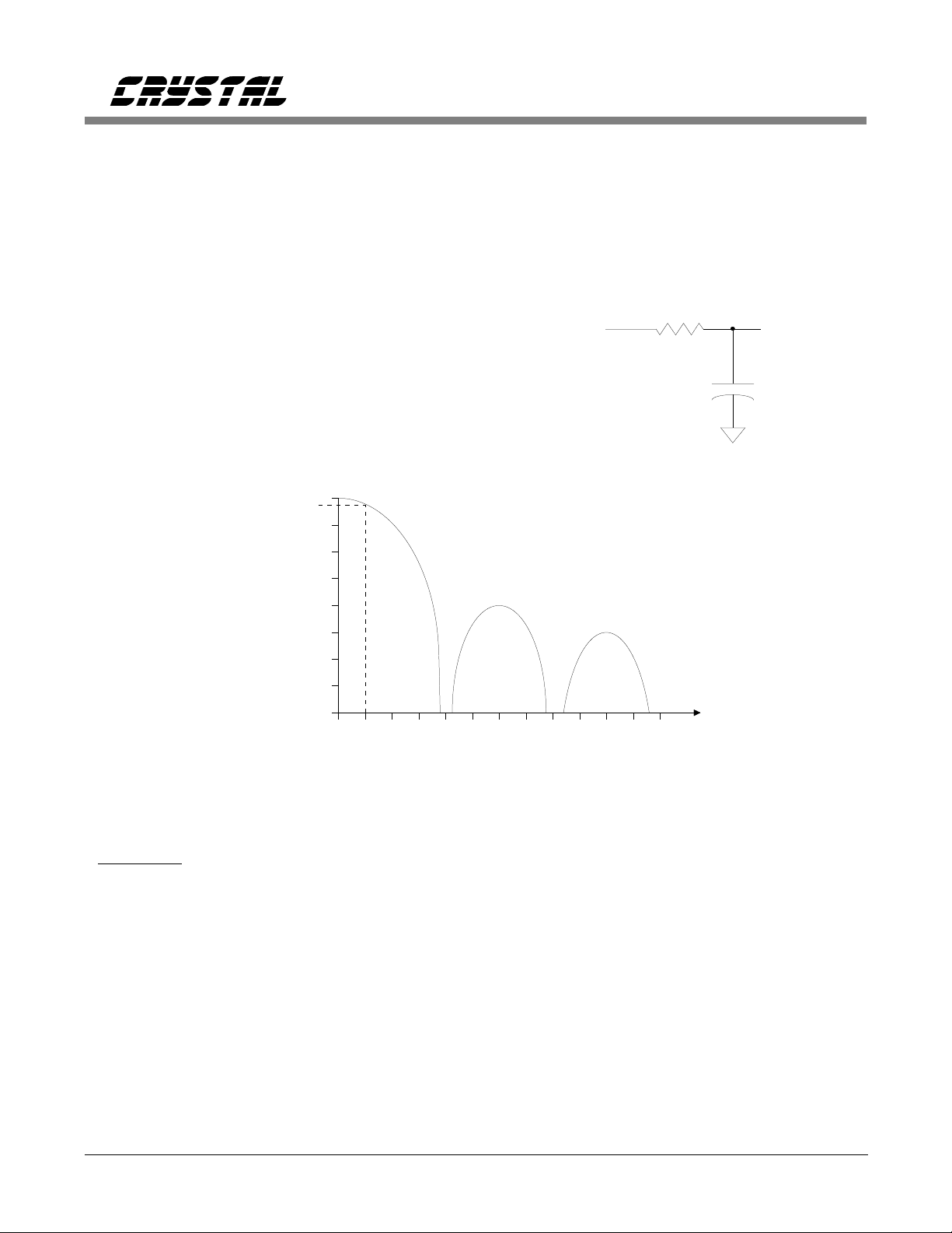
Figure 2. Anti-alias Filter
sin
128sin
128πƒ
(
T
(πƒT)
-40
-80
0 F 2F 3F
.25 F .5 F
dc
3
)
= Magnitude where: T = 1/
ƒ
sout
ƒ
sout
f
5 kHz
10 kHz
ƒ
= input sampling frequency = CLKOUT frequency for all modes
sin
= CLKIN/2 in CLKOR mode
= CLKIN*128 in CLKG1 mode
= CLKIN*256 in CLKG2 mode
F = ƒ
ƒ = input frequency
= ƒ
= ƒ
20 kHz
ƒ
sin
/128 for all modes
sin
/128 = output data rate for CLKOR & CLKG1 = F
sin
/256 = output data rate for CLKG2 = F/2
sin
40 kHz
60 kHz
Examples: For ƒ
For ƒ
DS27F4 9
= 2.56 MHz at ƒ = 5 kHz: Magnitude is -2.74 dB
sin
= 2.56 MHz at ƒ = 10 kHz: Magnitude is -11.8 dB
sin
Figure 3. CS5317 Low-Pass Filter Response
CS5317
Decimation
Aliasing effects due to decimation are identical in
the CLKOR and CLKG1 modes. Aliasing is different in the CLKG2 mode due to the difference
in output sample rates (10 kHz vs. 20 kHz) and
thus will be discussed separately.
Aliasing in the CLKOR and CLKG1 Modes
The delta-sigma modulator output is fed into the
digital low-pass filter at the input sampling rate,
f
. The filter’s frequency response is shown in
s
in
Figure 3. In the process of filtering the digitized
signal the filter decimates the sampling rate by
128 (that is, f
= f
s
out
/128). In its most elemen-
s
in
tary form, decimation simply involves ignoring or selectively reading - a fraction of the available
samples.
In the process of decimation the output of the
digital filter is effectively resa mp led at f
s
out
, the
output word rate, which has aliasing implications.
Residual signals after filtering at multiples of f
s
out
will alias into the baseband. For example, an input tone at 28 kHz will be attenuated by 39.9 dB.
If f
= 20 kHz, the residual tone will alias into
s
out
the baseband and appear at 8 kHz in the output
spectrum.
If the input signal contains a large amount of outof-band energy, additional analog and/or digital
antialias filtering may be required. If digital postfiltering is used to augment the CS5317’s
rejection above f
/4 (that is, above 5 kHz), the
s
out
filtering will also reject residual quantization
noise from the modulator. This will typically increase the converter’s dynamic range to 88 dB.
Further bandlimiting the digital output to f
/8
s
out
(2.5 kHz at full speed) will typically increase dynamic range to 90 dB.
Aliasing in the CLKG2 Mode
Aliasing effects in the CLKG2 mode can be modeled exactly as those in the CLKG1 mode with
the output decimated by two (from 20 kHz to 10
kHz). This is most easily achieved by ignoring
every other sample. In the CLKG2 mode the ratio
of the output sampling rate to the filter’s -3 dB
point is two, with no oversampling beyond the
demands of the Nyquist criterion. Without the
ability to roll-off substantially before f
s
out
/2, the
on-chip digital filter’s anti aliasing value is diminished.
The CLKG2 mode should therefore be used only
when the output data rate must be minimized due
to communication and/or storage reasons. In addition, adequate analog filtering must be provided
prior to the A/D converter .
Digital Design Considerations
The CS5317 presents its 16-bit serial output
MSB-first in 2’s complement format. The converter’s serial interface was designed to easily
interface to a wide variety of micro’s and DSP ’s.
Appendix A offers several hardware interfaces to
industry-standard processors.
f
out
DOUT
CLKOUT
DATA
10 DS27F4
15 14 15 14
MSB
(sign bit)
131211109876543210
LSB
Figure 4. Data O utput

CS5317
Data Output Characteristics & Coding Format
As shown in Figure 4, the CS5317 outputs its 16bit data word in a serial burst. The data appears at
the DATA pin on the rising edge of the same
CLKOUT cycle in which DOUT falls. Data
changes on the rising edge of CLKOUT, and can
be latched on the falling edge. The CLKOUT rate
is set by the CLKIN input (f
mode; f
f
*256 in the CLKG2 mode). DOUT returns
clkin
*128 in the CLKG1 mode; and
clkin
/2 in the CLKO R
clkin
high after the last bit is transmitted. After transmitting the sixteen data bits, DATA will remain
high until DOUT falls again, initiating the next
data output cycle.
A 3-state capability is available for bus-oriented
applications. The 3-state control input is termed
Data Output Enable, DOE, and is asynchronous
with respect to the rest of the CS5317. If DOE is
taken high at any time, even during a data burst,
the DATA, DOUT and CLKOUT pins go to a
high impedance state. Any data which would be
output while DOE is high is lost.
Power Supplies
Since the A/D converter’s output is digitally filtered in the CS5317, the device is more forgiving
and requires less attention than conventional 16bit A/D converters to grounding and layout
arrangements. Still, care must be taken at the design and layout stages to apply the device
properly. The CS5317 provides separate analog
and digital power supply connections to isolate
digital noise from its analog circuitry. Each supply pin should be decoupled to its respective
ground, AGND or DGND. Decoupling should be
accomplished with 0.1 µF ceramic capacitors. If
significant low frequency noise is present in the
supplies, 10 µF tantalum capacitors are recom-
mended in parallel with the 0.1 µF capacitors.
The positive digital power supply of the CS5317
must never exceed the positive analog supply by
more than a diode drop or the chip could be per-
manently damaged. If the two supplies are de-
rived from separate sources, care must be taken
that the analog supply comes up first at power-up.
Figure 1 shows a decoupling scheme which allows the CS5317 to be powered from a single set
of ± 5V rails. The digital supplies are derived
from the analog supplies through 10 Ω resistors
to prevent the analog supply from dropping below the digital supply.
PLL Characteristics
A phase-locked loop is included on the CS5317
and is used to generate the requisite high frequency A/D sampling clock. A functional
diagram of the PLL is shown in Figure 5. The
PLL consists of a phase detector, a filter, a VCO
(voltage-controlled oscillator), and a counter/di-
vider. The phase detector inputs are CLKIN (θ1)
and a sub-multiple of the VCO output signal (θ2).
The inputs to the phase detector are positive-edge
triggered and therefore the duty cycle of the
CLKIN signal is not significant. With this type of
phase detector, the lock range of the PLL is equal
to the capture range and is independent of the low
pass filter. The output of the phase detector is input to an external low pass filter. The filter
characteristics are used to determine th e transient
response of the loop. The output voltage from the
filter functions as the input control voltage to the
VCO. The output of the VCO is then divided in
frequency to provide an input to the phase detector. The clock divider ratio is a function of the
PLL mode which has been selected.
Phase Detector Gain (Kd)
A properly designed and operating phase-locked
loop can be described using steady state linear
analysis. Once in frequency lock, any phase difference between the two inputs to the phase
detector cause a current output from the detector
during the phase error. While either the +50 µA or
the -50 µA current source may be turned on, the
average current flow is:
DS27F4 11

CS5317
i
= Kd(θ1−θ2) ≈ (−50µA ⁄ 2π) (θ1−θ2)
out
avg
where θ1 is the phase of IN1, θ2 is the phase of
IN2 and Kd is the phase detector gain. The factor
2π comes from averaging the current over a full
CLKIN cycle. Kd is in units of micro-am-
peres/radian.
VCO Gain (Ko)
The output frequency from the VCO ranges from
1.28 MHz to 5.12 MHz. The frequency is a function of the control voltage input to the VCO. The
VCO has a negative gain factor, meaning that as
the control voltage increases more positively the
output frequency decreases. The gain factor units
are Megaradians per Volt per Second. This is
equivalent to 2π Megahertz per volt. Changes in
output frequency are given by:
∆ω
= Ko ∆VCOin [Ko is typ. -10Mrad/Vs.]
vco
Counter/Divider Ratio
The CS5317 PLL multiplies the CLKIN rate by
an integer value. To set the multiplication rate, a
counter/divider chain is used to divide the VCO
output frequency to develop a clock whose frequency is compared to the CLKIN frequency in
the phase detector. The binary counter/divider ra-
tio sets the ratio of the VCO frequency to the
CLKIN frequency. As illustrated in Figure 5, the
VCO output is always divided by two to yield the
CLKOUT signal which is identical in frequency
to the delta-sigma modulator sampling clock.
The CLKOUT signal is then further divided by
either 128 in the CLKG1 mode or by 256 in the
CLKG2 mode. When the divide by two stage is
included, the divider ratio (N) for the PLL in the
CLKG1 mode is effectively 256. In the CLKG2
mode the divider ratio (N) is 512.
Loop Transfer Function
As the phase-locked loop is a closed loop system,
an equation can be determined which describes its
closed loop response. Using the gain factors for
the phase detector and the VCO, the filter arrangement and the counter/divider constant N,
analysis will yield the following equation which
describes the transfer function of the PLL:
KoKdR
θ
2
=
θ
1
s2 +
N
KoKdR
N
s +
s +
KoKd
NC
KoKd
NC
This equation may be rewritten such that its elements correspond with the following
+5V
Kd=
-8 µA/rad
1
CLKIN
12 DS27F4
IN1
Phase/Frequency
Detect Logic
IN2
2
Conversion Output Rate Same Frequency as DOUT
DOWN
UP
50
50 µA
-5V
Figure 5. PLL Funct ional Dia gram
VA+
µ
A
C
2
PHDT
VCOIN
CLKG2
CLKG1
C
R
External RC
VCO
CLKOR
K0= -10 Mrad/V.s
2
128
Internal Sync for Digital Filter
CLKOR
2
Delta-Sigma
Sampling Cloc k
(CLKOUT)

CS5317
characteristic form in which the damping factor,
ζ, and the natural frequency, ωn , are evident:
s + ω
n
2
2
n
θ
2
θ
1
2ζωns + ωn
=
s2 + 2ζω
Bo th the natural f reque ncy and the dampi ng f actor are particularly important in determining the
transient response of the phase-locked loop when
subjected to a step input of phase or frequency. A
family of curves are illustrated in Figure 6 that
indicate the overshoot and stability of the loop as
a function of the damping factor. Each response is
plotted as a function of the normalized time, ωn t.
For a given ζ and lock time, t, the ωn required
can be determined. Alternatively, phase lock control loop bandwidth may be a specified parameter.
In some systems it may be desirable to reduce the
-3dB bandwidth of the PLL control loop to reduce the effects of jitter in the phase of the input
clock. The 3 dB bandwidth of the PLL control
loop is defined by the following equation:
CLKIN is approximately 20 times greater than
the 3 dB corner frequency of the control loop.
Filter Components
Using the equations which describe the transfer
function of the PLL system, the following external filter component equations can be determined:
KoKd
C =
R = 2ζωn
Nω
2
n
N
KoKd
The gain factors (Ko, Kd) are specified in the
Analog Characteristics table. In the event the system calls for very low bandwidth, hence a
corresponding reduction in loop gain, the phase
detector gain factor Kd can be reduced. A large
series resistor (R1) can be inserted between the
output of the detector and the filter. Then the
50 µA current sources will saturate to the supplies
and yield the following gain factor:
ω
3dB
= ω
√2ζ
n
2
+ 1 +
√(2ζ
2
+ 1)2 + 1
The equations used to describe the PLL and the
3 dB bandwidth are valid only if the frequency of
θ2 normalized to θ
1.3
1.2
1.1
1.0
0.9
0.8
0.7
0.6
0.5
0.4
0.3
0.2
0.1
0.0
012345678910
1
ζ= 0.5
ζ= 10.0
ωn t.
Figure 6a. θ2 Unit Step Response
−5V
2πR
ω/ω
1
ζ = 0.5
n
20 log(θ2/θ1)
ζ = 0.5
ζ = 0.6
ζ = 0.7
ζ = 0.8
ζ = 0.9
ζ = 1.0
ζ = 1.5
ζ = 2.0
ζ = 3.0
ζ = 10.0
Kd ≈
4
3
2
1
0
-1
-2
-3
-4
-5
-6
-7
-8
-9
-10
0.1 1 10
Figure 6b. Second Order PLL Frequency Response
ζ = 10
DS27F4 13

CS5317
In some applications additional filtering may be
useful to eliminate any jitter associated with the
discrete current pulses from the phase detector.
In this case a capacitor whose value is no more
than 0.1 C can be placed across the RC filter network (C2 in Figure 5).
Filter Design Example
The following is a step by step example of how to
derive the loop filter components. The CS5317
A/D sampling clock is to be derived from a 9600
Hz clock source. The application requires the signal passband of the CS5317 to be 4 kHz. The
on-chip digital filter of the CS5317 has a 3 dB
passband of CLKOUT/488.65 (see Note 4 in the
data sheet specifications tables). The 4 kHz passband requirement dictates that the sample clock
(CLKOUT) of the CS5317 be a minimum of
4000 X 488.65 = 1.954 MHz. This requires the
VCO to run at 3.908 MHz. The 3.908 MHz rate is
407 times greater than the 9600 Hz PLL input
clock. Therefore the CS5317 must be set up in
mode CLKG2 with N = 512. If the CLKG1 mode
were used (N = 256), too narrow of a signal bandwidth through the A/D would result.
To calcul ate values for the resistor R and capacitor C of the filter, we must first derive a value for
ωn. Using the general rule that the sample clock
should be at least 20 times higher frequency than
the 3dB bandwidth of the PLL control loop:
CLKIN ≥ 20 ω
3dB
where CLKIN = 9600 Hz = 2π 9600 radians/sec.
So: ω
Knowing ω
= 2π 9600/20 = 3016 radians/sec.
3dB
and the damping factor of 1.0, we
3dB
can calculate the natural frequency, ωn , of the
control loop:
ωn = ω
3dB
√2ζ
2
+ 1 +
√(2ζ
2
+ 1)2 + 1
ω
= 3016 √2(1)
n
2
+ 1 +
√(2(1)
2
+ 1)2 + 1
ωn = 1215 1 ⁄ sec
Once the natural frequency, ωn , is determined,
values for R and C for the loop filter can be calculated:
Once the operating mode has been determined
from the system requirements, a value for the
R = 2ζωnN/KoKd
damping factor must be chosen. Figure 6 illustrates the dynamic aspects of the system with a
R = 2(1)(1215 1/s) 512/(-10Mrad/v.s.)(-8 µA/rad)
given damping factor. Damping factor is generally chosen to be between 0.5 and 2.0. The choice
of 0.5 will result in an overshoot of 30 % to a step
response whereas the choice of 2.0 will result in
R = 15552 v/A = 15.55 kΩ. Use R = 15 kΩ.
C = KoKd/Nω
2
n
an overshoot of less than 5 %. For example purposes, let us use a damping factor of 1.0.
So, let us begin with the following variables :
Ko = - 10 Mradians/volt.sec
Kd = - 8 µA/radian
N = 512
ζ = 1.0
C = (-10 Mrad/v.s)(- 8 µA/rad)/512 (1215 1/s)
C = 105.8 x 10 -9 A.s/v = 105 nF. Use 0.1 µF.
The above example assumed typical values for
Ko and Kd. Your application may require a worst
case analysis which includes the minimum or
maximum values. Table 2 shows some other ex-
2
ample situations and R and C values.
14 DS27F4

CS5317
CLKIN
(Hz) Mode N
7200 CLKG2 512 1.8432 1.0 2262 911 11.6 187
9600 CLKG2 512 2.4576 1.0 3016 1215 15.5 106
14400 CLKG1 256 1.8432 1.0 4524 1822 11.6 94
19200 CLKG1 256 2.4576 1.0 6032 2430 15.5 52
* The values for R and C are as calculated using the described method. Component tolerances have
not been allowed for. Notice that Ko and Kd c an vary over a wide range, so using tight tolerances
for R and C is not justified. Use the nearest conveniently available value.
Table 2 Example PLL Loop Filter R and C values
CS5317 PERFORMANCE
CLKOUT
(MHz)
ζω
3dB
ω
n
R * (kΩ)C * (nF)
The quality of the window used for harmonic
analysis is typically judged by its highest side-
The CS5317 features 100% tested dynamic performance. The following section is included to
illustrate the test method used for the CS5317.
FFT Tests and Windowing
lobe level. The Blackman-Harris window used to
test the CS5317 has a maximum side-lobe level
of -92 dB.
Figure 7 shows an FFT plot of a typical CS5317
with a 1 kHz sinewave input generated by an "ul-
The CS5317 is tested using Fast Fourier Trans-
form (FFT) techniques to analyze the converter’s
dynamic performance. A pure sine wave is applied to the CS5317 and a "time record" of 1024
samples is captured and processed. The FFT algorithm analyzes the spectral content of the digital
waveform and distributes its energy among 512
"frequency bins". Assuming an ideal sinewave,
distribution of energy in bins outside of the fundamental and dc can only be due to quantization
effects and errors in the CS5317.
tra-pure" sine wave generator and the output
multiplied by a Blackman-Harris window. Artifacts of windowing are discarded from the
signal-to-noise calculation using the assumption
that quantization noise is white. All FFT plots in
this data sheet were derived by averaging the FFT
results from ten time records. This filters the
spectral variability that can arise from capturing
finite time records, without disturbing the total
energy outside the fundamental. All harmonics
and the -92 dB side-lobes from the BlackmanHarris window are therefore clearly visible in the
If sampling is not synchronized to the input sine-
plots.
wave it is highly unlikely that the time record will
contain an exact integer number of periods of the
input signal. However, the FFT assumes that the
signal is periodic, and will calculate the spectrum
0dB
-20dB
-40dB
Sampling Rate: 19.2 kHz
Full Scale:
S/(N+D): 81.39 dB
of a signal that appears to have large discontinuities, thereby yielding a severely distorted
spectrum. To avoid this problem, the time record
is multiplied by a window function prior to performing the FFT. The window function smoothly
forces the endpoints of the time record to zero,
removing the discontinuities. The effect of the
"window" in the frequency domain is to convo-
Signal
Amplitude
Relative to
Full Scale
-60dB
-80dB
-100dB
-120dB
dc
Input Frequency
lute the spectrum of the window with that of the
actual input.
Figure 7. CS5317 Dynamic Performance
+ 2.75 V_
9.6 kHz1 kHz
DS27F4 15

CS5317
Full - scale signal - to - noise - plus - distortion
[S/(N+D)] is calculated as the ratio of the rms
power of the fundamental to the sum of the rms
power of the FFT’s other frequency bins, which
include both noise and distortion. For the
CS5317, signal-to-noise-plus-distortion is shown
to be better than 81 dB for an input frequency
range of 0 to 9.6 kHz (fs/2).
Harmonic distortion characteristics of the CS5317
are excellent at 80 dB full scale signal to THD
(typical), as are intermodulation distortion characteristics, shown in Figure 8. Intermodulation
distortion results from the modulation distortion
of two or more input frequencies by a non-linear
transfer function.
DNL Test
Figure 9 shows a plot of the typical differential
non-linearity (DNL) of the CS5317. This test is
done by taking a large number of conversion results, and counting the occurrences of each code.
A perfect A/D converter would have all codes of
equal size and therefore equal numbers of occurrences. In the DNL test, a code with the average
number of occurrences is considered ideal and
plotted as DNL = 0 LSB. A code with more or
less occurrences than average will appear as a
DNL of greater than or less than zero. A missing
code has zero occurrences, and will appear as a
DNL of -1 LSB.
0dB
S/I.M.D.: 84.7 dB
Signal
Amplitude
Relative to
Full Scale
-20dB
-40dB
-60dB
-80dB
-100dB
-120dB
800 1450 9600
dc
Input Frequency (Hz)
Figure 8. CS5317 Intermodulation D istortion
The plot below illustrates the typical DNL per-
formance of the CS5317, and clearly shows the
part easily achieves no missing codes.
Schematic & Layout Review Service
Confirm Optimum
Confirm Optimum
Schematic & Layout
Schematic & Layout
Before Building Your Board.
Before Building Your Board.
For Our Free Review Service
For Our Free Review Service
Call Applications Engineering.
Call Applications Engineering.
Call:(512)445-7222
+1
+1/2
0
DNL (LSB)
-1/2
-1
0 65,535
32,768
Codes
Figure 9. CS5317 DNL Plot
16 DS27F4

PIN DESCRIPTIONS (Pin numbers refer to the 18 -pin DIP pack age)
18 pin DIP Pinout
CS5317
POSITIVE ANALOG PO WER VA+ VCOIN VCO INPUT
POSITIVE DIGITAL POWER VD+ PHDT PHASE DETECT
DATA OUTP UT ENA BLE
DIGITAL GROUND DGND AGND ANALOG GROUND
SERIAL CLOCK OUTPUT CLKOUT VA- NEGATIVE ANALOG POWER
SERIAL DATA OUTPUT DATA NC NO CONNECT
CLOCKING MODE SELECT MODE REFBUF POSITIVE REFERENCE BUFFER
DATA OUTPUT READY
20 pin SOIC pinout
POSITIVE ANALOG PO WER VA+ VCOIN VCO INPUT
POSITIVE DIGITAL POWER VD+ PHDT PHASE DETECT
DATA OUTP UT ENA BLE
DIGITAL GROUND DGND AGND ANALOG GROUND
SERIAL CLOCK OUTPUTCLKOUT NC NO CONNECT
SERIAL DATA OUTPUT DATA VA- NEGATIVE ANALOG POWER
CLOCKING MODE SELECT MODE REFBUF POSITIVE REFERENCE BUFFER
DATA OUTPUT READY
Power Supplies
18
1
17
2
DOE RST RESET
DOUT AIN ANALOG INPUT
CLOCK INPUT CLKIN VD- NEGATIVE DIGITAL POWER
1
2
DOE RST RESET
NO CONNECT NC NC NO CONNECT
DOUT AIN ANALOG INPUT
CLOCK INPUT CLKIN VD- NEGATIVE DIGITAL POWER
3
4
5
6
7
8
9
10
16
3
15
4
14
5
13
6
12
7
11
8
109
20
19
18
17
16
15
14
13
12
11
VD+ - Positive Digital Power, PIN 2.
Positive digital supply voltage. Nominally 5 volts.
VD- - Negative Digital Power, PIN 10.
Negative digital supply voltage. Nominally -5 volts.
DGND - Digital Ground, PIN 4.
Digital ground reference.
VA+ - Positive Analog Power, PIN 1.
Positive analog supply voltage. Nominally 5 volts.
VA- - Negative Analog Power, PIN 14.
Negative analog supply voltage. Nominally -5 volts.
AGND - Analog Ground, PIN 15.
Analog ground reference.
PLL/Clock Generator
CLKIN - Clock Input, PIN 9.
Clock input for both clock generation modes and the clock override mode (see MODE).
DS27F4 17

MODE - Mode Set, PIN 7.
Determines the internal clocking mode utilized by the CS5317. Connect to +5V to select
CLKG1 mode. Connect to DGND to select CLKG2 mode. Connect to -5V to select CLKOR
mode. This pin becomes equivalent to FSYNC in the CS Z5316 compatible mode.
VCOIN - VCO Input, PIN 18.
This pin is typically connected to PHDT. A capacitor and resistor in series connected between
VA+ and this pin sets the filter response of the on-chip phase locked loop.
PHDT - Phase Detect, PIN 17.
This pin is typically connected to VCOIN. A capacitor and resistor in series connected between
VA+ and this pin sets the filter response of the on-chip phase locked loop.
Inputs
AIN - Analog Input, PIN 11.
DOE - Data Output Enable, PIN 3.
Three-state control for serial output interface. When low, DATA, DOUT, and CLKOUT are
active. When high, they are in a high impedance state.
CS5317
RST - Sample Clock Reset, PIN 16.
Sets phase of CLKOUT. Functions only in the clock override mode, CLKOR. Used to
synchronize the output samples of multiple CS5317’s. Must be kept high in CLKG1 or CLKG2
modes. Also, tying this pin low, with MODE not tied to - 5V, will place the CS5317 into
CSZ5316 compatible mode.
Outputs
DOUT - Data Output Flag, PIN 8.
The falling edge indicates the start of serial data output on the DATA pin. The rising edge
indicates the end of serial data output.
DATA - Data Output, PIN 6.
Serial data output pin. Converted data is clocked out on this pin by the rising edge of
CLKOUT. Data is sent MSB first in two’s complement format.
CLKOUT - Data Output Clock, PIN 5.
Serial data output clock. Data is clocked out on the rising edge of this pin. The falling edge
should be used to latch data. Since CLKOUT is a free running clock, DOUT can be used to
indicate valid data.
REFBUF - Positive Voltage Reference Noise Buffer, PIN 12.
Used to attenuate noise on the internal positive voltage reference. Must be connected to the
analog ground through a 0.1µF ceramic capacitor.
18 DS27F4

CS5317
PARAMETER DEFINITIONS
Resolution - The number of different output codes possible. Expressed as N, where 2N is the number
of available output codes.
Dynamic Range - The ratio of the largest allowable input signal to the noise floor.
Total Harmonic Distortion - The ratio of the rms sum of al l harmonics to the rms value of th e largest
allowable input signal. Units in dB’s.
Signal to Intermodulation Distortion - The ratio of the rms sum of two input signals to the rms sum
of all discernible intermodulation and harmonic dist ortion products.
Linearity Error - The deviation of a code from a straight line passing through the endpoints of the
transfer function after zero- and full-scale errors have been accounted for. "Zero-scale" is a
point 1/2 LSB below the first code transition and "full-scale" is a point 1/2 LSB beyond the
code transition to all ones. The deviation is measured from the middle of each particular code.
Units in %FS.
Differential Nonlinearity - The deviation of a code’s width from the ideal width. Units in LSB’s.
Positive Full Scale Error - The deviation of the last code transition from the ideal, (VREF - 3/2 LSB).
Units in mV.
Positive Full Scale Drift - The drift in effective, positive, full-scale input voltage with temperature.
Negative Full Scale Error - The deviation of the first code transition from the ideal, (-VREF + 1/2
LSB). Units in mV.
Negative Full Scale Drift - The drift in effective, negative, full-scale input voltage with temperature.
Bipolar Offset - The deviation of the mid-scale transition from the ideal. The ideal is defined as the
middle transition lying on a straight line between actual positive full-scale and actual negative
full-scale.
Bipolar Offset Drift - The drift in the bipolar offset error with temperature.
Absolute Group Delay - The delay through the filter section of the part.
Passband Frequency - The upper -3 dB frequency of the CS5317.
DS27F4 19

ORDERING GUIDE
Model Number Temperature Range Package
CS5317-KP 0 to 70°C 18 Pin Plastic DIP
CS5317-KS 0 to 70°C 20 Pin Plastic SOIC
CS5317
20 DS27F4

CS5317
APPENDIX A
APPLICATIONS
CS5317
DATA
CLKOUT
DOUT
A
S1
S2
Q
H
+5V
OE2
A
S1
S2
Figure A1 shows one method of converting the
serial output of the CS5317 into 16-bit, parallel
words. The associated timing is also shown.
+5V
OE2
P
D0
A
P
D1
B
P
D2
74HCT299
OE1
OE1
74HCT299
C
P
D3
D
P
D4
E
P
D5
F
P
D6
G
P
D7
H
P
D8
A
P
D9
B
P
D10
C
P
D11
D
P
D12
E
P
D13
F
P
D14
G
P
D15
H
8
16
8
Data
Bus
CS
SET
D
Q
74HCT74
Q
INT
INT
Only needed for level sensitive interrupt driven systems.
CLKOUT
DOUT
15 13
DATA
INT
14
(MSB)
INT Cleared when data read
02 1
(CS goes low)
Figure A1. CS5317-t o-Parallel Dat a Bus Interface
DS27F4 21

CS5317
Figure A2 shows the interconnection and timing
details for connecting a CS5317 to a NEC
µPD7730 DSP chip.
Status Register (SR)
Bit
Mnemonic
9
7, 6
3
CLKOUT
DOUT
DATA
Setting
SCI
SDLI
SIF
Meaning
External Clock
0
16 bit data
1, 0
MSB First
0
15 13
(MSB)
Figure A2. CS5317-to-NEC µPD77230 Serial Interface
14
Figure A3 shows the interconnection and timing
details for connecting a CS5317 to a Motorola
DSP 56000.
1
CS5317
CLKOUT
DOUT
DATA
02
PD77230
µ
SICK
SIEN
SI
SSI Control Reg. A
CRA (X:FFEC)
WL1 = 1
WL0 = 0
CLKOUT
DOUT
16 bits
SYNC
CLKOUT
PINS
(MSB)
Figure A3. CS53 17-to- Motoro la DSP560 00 Seria l Interface
DOUT
GCK
SYN
FSL
SCKD
SCD2
SCD1
CRB (X:FFED)
SSI Control Reg. B
SCD0
15 1314DATA
SCK
SC2
0
1
0
0
0
-
-
ASYNC
SC0
SC1
0
0
0
-
0
0
CS5317
CLKOUT
DOUT
DATA
02 1
DSP56000
SCK, SC0
SC2, SC1
SRD
22 DS27F4

CS5317
Figure A4 shows the interconnection and timing
details for connecting a CS5317 to a WE DSP16
DSP chip.
Serial I/O Control Register (SIOC)
Field
MSB
ILD
ICK
ILEN
CLKOUT
DOUT
DATA
d
Value
Meaning
MSB input first
1
ILD is an input
0
ICK is an input
0
16 bit input data
0
15 1314 2 1 0
(MSB)
Figure A4. CS5317-to-WE DSP16 Serial Interface
Figure A5 shows the interconnection and timing
details for connecting a CS5317 with TMS32020
and TMS320C25 DSP chips.
CS5317
CLKOUT
DOUT
DATA
74
QD
DATA
d
DSP16
ICK
ILD
DI
TMS32020
TMS320C25
CLKR
FSR
DR
TMS32020 Status Register (ST1):
F0 = 0 (16 bit data)
TMS320C25 Status Register (ST1):
F0 = 0 (16 bit data)
FSM = 1 (Frame Sync used)
CLKOUT
DOUT
15 1314DATA
(MSB)
CS5317
CLKOUT
DOUT
DATA
02 1
Figure A5. CS5317-to-TMS32020/TMS320C25 Serial Interface
DS27F4 23

• Notes •

Evaluation Board for CS5317
CDB5317
Features
l
Easy to Use Digital Interface
Parallel 16 Bits With Clock
Serial Output With Clock
l
Multiple Operating Modes
Including Two PLL Modes
l
IDC Header used to access Parallel Data,
Serial Data, and Clock Input and Output
I
AIN
Description
The CDB5317 Evaluation Boar d is des igned to al low the
user to quickly evalu ate performance of the CS5317 Delta-Sigma Analog-to-Digi tal Converter. All that is required
to use this board is an external power supply, a signal
source, a clock sour ce, and an ability to read ei ther serial
or parallel 16bitdata words.
ORDERING INFORMATION
CDB5317 Evaluation Board
+5V
GND
-5V
V
L
CLKIN
Cirrus Logic, Inc.
Crystal Semiconductor Products Division
P.O. Box 17847, Austin, Texas 78760
(512) 445 7222 FAX: (512) 445 7581
http://www.crystal.com
CLKIN
CLKOUT
CS5317
IDC HEADER
Copyright Cirrus Logic, I nc. 1998
(All Rights Reserv ed)
DATA
SERIAL TO PARALLEL
CONVERTER
DRDY
DACK
D0-D15
MAR ‘95
DS27DB3
25

CDB5317
GENERAL DESCRIPTION
The CDB5317 Evaluation Board is a stand-alone
environment for easy lab evaluation of the
CS5317 Delta-Sigma Analog-to-Digital Converter.
Included on the board is a serial-to-parallel converter. The user can access output data in either
parallel or serial form. When supplied with the
necessary +5 V and -5 V power supplies, a
CLKIN signal, and an analog signal source, the
CDB5317 will provide converted data at the 40
pin header.
SUGGESTED EVALUATION METHOD
An efficient evaluation of the CS5317 using the
CDB5317 may be accomplished as described below.
The following equipment will be required for the
evaluation:
• The CDB5317 Evaluation Board.
• A power supply capable of supplying +5V and
-5V.
• A clock source as the CLKIN signal of the
CS5317.
• A spectrally pure sine wave generator such as
the Krohn-Hite Model 4400A "Ultra-Low Distortion Oscillator".
• A PC equipped with a digital data acquisition
board such as the Metrabyte Model PIO12 "24 Bit
Parallel Digital I/O Interface".
• A software routine to collect the data and perform a Fast Fourier Transform (FFT).
The evaluation board includes filter components
for the on-chip phase locked loop. The components are adequate for testing if the CLKIN signal
has little or no phase-jitter. If the CDB5317 board
is being tested as part of a system which generates
a CLKIN which contains jitter, the PLL filter
components may need to be optimized for your
system (see the CS5317 data sheet).
Set-up for evaluation is straightforward. First decide the operating mode and place the jumper on
the board for the proper selection. Then decide
whether the filter components for the phase
locked loop are adequate or whether they should
be changed for your evaluation. The PLL will
lock on a steady clock input with the filter as it is.
Connect the necessary 5 V (CMOS compatible)
CLKIN signal for the application. Use the sinewave generator to supply the analog signal to the
CDB5317. Apply the analog input and CLKIN
signals only when the evaluation board is powered up. Converted data will then appear at the
header on the CDB5317. The header should be
connected to the digital data acquisition board in
the PC through an IDC 40 pin connector and cable. The software routine should collect the data
from the CDB5317 and run a standard 1024 point
Fast Fourier Transform (FFT). Such an analysis
results in a plot similar to Figure 1. This plot resulted from using a 1kHz input signal and a
Blackman-Harris window for the FFT.
The signal to noise and signal to total harmonic
distortion characteristics of the CS5317 may be
easily measured in this way. The signal to total
harmonic distortion value for a particular input is
the ratio of the RMS value of the input signal and
the sum of the RMS values of the harmonics
shown in the diagram. The dynamic range of the
CS5317 can be measured by reducing the input
Signal
Amplitude
Relative to
Full Scale
0dB
-20dB
-40dB
-60dB
-80dB
-100dB
-120dB
dc
1 kHz
Input Frequency
Sampling Rate: 19.2 kHz
Full Scale:
S/(N+D): 81.39 dB
± 2.75 V
9.6 kHz
Figure 1. FFT Plot Example
26 DS27DB3

CDB5317
amplitude so that distortion products become negligible. This allows an accurate measurement of
the noise floor.
More complex analysis such as intermodulation
distortion measurements can be accomplished
with the addition of another sine-wave generator.
CIRCUIT DESCRIPTION
Figure 2 illustrates the CS5317 A/D converter IC
circuit connections. The chip operates off of ±5V.
These voltages are supplied from a power source
external to the evaluation board. Binding posts
TP6
V
L
µ
F
C8
C9
10µF
0.1 µF
17
18
9
11
12
C14
0.1 µF
C15
0.1 µF
15
+5V
CLKIN
AIN
GND
-5V
6.8v
V
L
D1
0.1 µF
TP10
C19 C17
D3
R2
200
R1*
51
TP9
* Remove for logic gate CLKIN source
CLKIN (fig.6)
R11
1.2k
TP7
0.22µF
R10
10k
C18
0.01 µF
NPO
D2
6.8v
C4C5
10
TP8
C16
10µF
are supplied on the board to connect the +5, -5,
and ground power lines. A good quality low ripple, low noise supply will give the best
performance. The +5 V supply can also be used
for VL and should be connected between the VL
board jack and the power supply, as opposed to
connecting the VL jack straight to the +5V jack.
The +5V jack is the positive power source for the
CS5317 IC whereas the VL jack supplies power
to all the digital ICs. Care should be taken that
noise is not coupled between VL and +5V; however, supply noise is generally not a problem with
the CS5317 since the on-chip decimation filter
will remove any interference outside of its passband. The +5 and -5 V supply lines are filtered on
R7
10
1
VA+
PHDT
VCOIN
CLKIN
U6
AIN
REFBUF
CS5317
AGND
VA-
14
R8
10
2
VD+
DOE
DOUT
CLKOUT
DATA
RST
MODE
DGND
VD-
10
C6
+
10 µF
8
5
6
0.1
µ
R5
10 k
R9
10 k
F
3
16
7
4
C13 C1 2
CLKG1
CLKG2
CLKOR
+
10 µF
C7
0.1 µF
DOUT
CLKOUT
DATA
R6
10 k
P2
(fig. 3)
(fig. 3)
(fig. 3)
Figure 2. Analog-to-Digital Conve rter
DS27DB3 27

CDB5317
the board and then connected to the VA+ and VAsupply pins of the chip. The +5 V and -5V are
then connected by means of ten Ω resisto rs to the
VD+ and VD- pins respectively. Capacitive filtering is provided on all supply pins of the chip. In
addition there is a 0.1 µF filter capacitor connected from the REFBUF pin of the chip to the
VA- supply pin.
To properly operate, the CS5317 chip requires an
external (5 V CMOS compatible) clock. A BNC
connector labeled CLKIN is provided to connect
the off-board clock signal to the board. The
CLKIN signal is also available on the 40 pin
header connector. The CLKIN signal is one input
U5
1
3
9
11
13
UNUSED GATES
VL
VL
VL
12
11
VL
D
CL
S
U4
R
13
10
12
10
2
4
8
Q
Q
DOUT
(fig. 2)
CLKOUT
(fig. 2)
9
DATA
8
(fig. 2)
V
L
14
1
2
7
3
U1
11 10 9
C1
0.1 µF
13
4
to the phase detector of the on-chip phase locked
loop of the CS5317.
Header connector P2 (see Figure 2) is provided to
allow mode selection for the CS5317 chip. The
mode selection works together with the CLKIN
signal to set the sample rate and the output word
rate of the CS5317. See the CS5317 data sheet
for details on mode selection. Two of the available modes (CLKG1 and CLKG2) utilize the
on-chip phase locked loop to step up the CLKIN
frequency to obtain the necessary sample rate
clock for the A/D converter. Another mode (the
CLKOR mode) does not use the on-chip PLL but
instead drives the sample function directly. The
V
L
C10
Q
Q
0.1 µF
6
5
6
C11
0.1 µF
D
V
L
14
U5
7
TP2
5
V
L
R4
10k
TP3
4
14
D
74HC74
CL
GND R
7
S
U4
2
12
5
6
8
3
DOUT2
(fig. 6)
DRDY
(fig. 6)
DACK
(fig. 6)
CLKOUT
(fig. 6)
CLKOUT2
(fig. 6)
DATA 1
(fig. 6)
DATA
(fig. 6)
Figure 3. Buffers and Parallel Handshake Flip-Flop
28 DS27DB3

CLKOUT
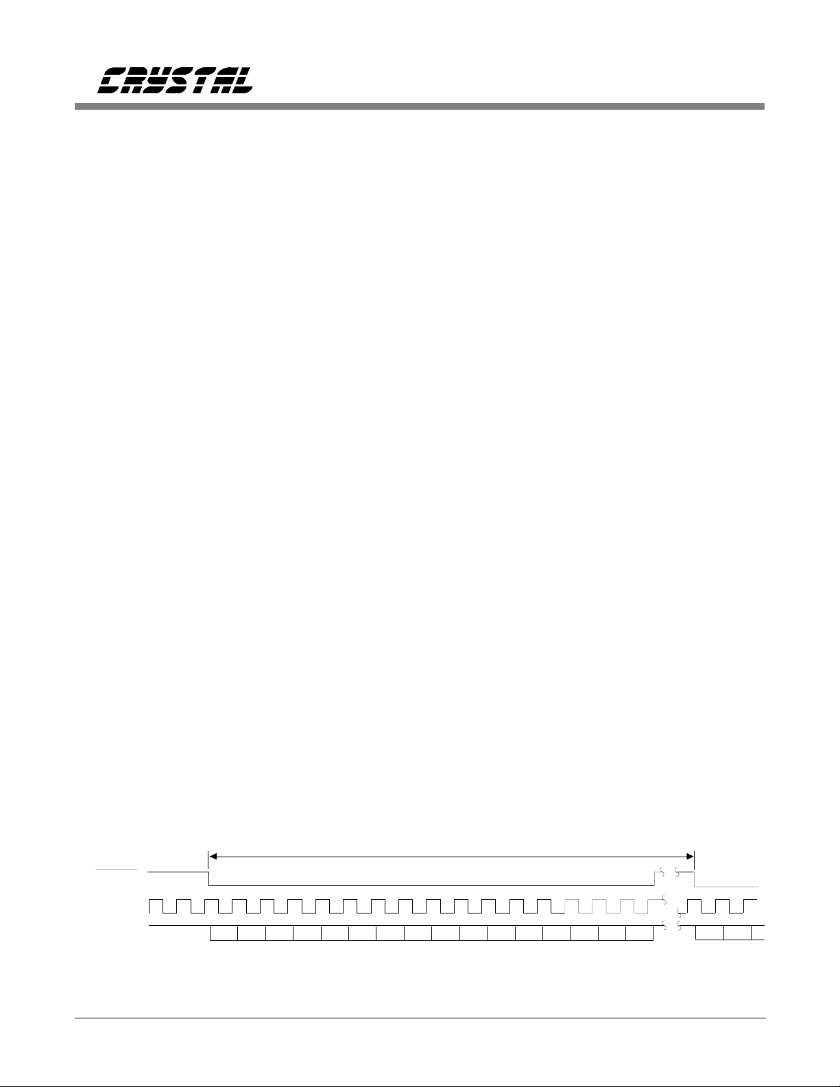
CDB5317
DATA
DOUT
Note: For a complete description of serial timing see the CS5317 Data Sheet
1514131211109876543210
Figure 4 Serial Data Timing
two modes which use the phase locked loop will
require appropriate low pass filter components on
the Evaluation Board. The low pass filter components help determine the PLL control loop
response, including its bandwidth and stability
and therefore directly affect the transient response
of the PLL control loop. Appropriate filter components should be installed if a particular dynamic
response to changes of the CLKIN signal is desired.
The filter components which are installed on the
board have been chosen for the following parameters: MODE: CLKG2; CLKIN: 7,200; N=512;
damping factor: 1.0; Control loop -3 dB bandwidth: 2262 radians/second. These parameters
yield R as 10 k Ω and C as 0.22 µF for the filter
components.
The analog signal to be digitized is input to the
AIN BNC connector. The digital output words
from the CS5317 are buffered by HEX inverters
as shown in Figure 3. The buffered versions of
the CLKOUT and DATA signals are available on
the header connector P1 in Figure 6. The serial
data signals out of the CS5317 are illustrated in
Figure 4. If remote control of the DOE line is
desired, the trace on the PC Board can be opened
and a wire connection can be soldered to the DOE
input line. Remote control of the RST line of the
CS5317 is also available if desired.
Figures 5 and 6 illustrate the serial to parallel shift
registers including timing information. The DATA
output signal from the CS5317 is input to the data
input of the shift register. An inverted version of
the CLKOUT signal is used to clock the DATA
into the shift registers . The two 8-bit shift register
ICs also include output latches. The rising edge
Serial Data
Shifting Out Parallel Data (D0-D15) Valid
DATA
DOUT
DRDY
DACK
Figure 5. Parallel Data Timing
DS27DB3 29
Serial Data
Shifting Out
Parallel Data Valid

CDB5317
of the DOUT signal from the CS5317 is used to
latch the data once it is input to the shift registers.
The rising edge of DOUT is also used to toggle
the DRDY flip flop (see Figure 3). The flip flop
is used to signal a remote device whenever new
CLKIN
(fig. 2)
CLKOUT2
(fig. 3)
V
L
10 16
RST
74HC595
U2
GND
8
OE
DATA1
(fig. 3)
TP4
TP5
12
LATCH CLK
11
SHIFT CLK
14
DIN
C2
0.1 µF
QH
QG
QF
QE
QD
QC
QB
QA
13
data is latched into the output registers. The
DRDY flip flop is reset whenever DACK occurs.
A component layout of the CDB5317 board is illustrated in Figure 7.
P1
CLKIN
CLKOUT
DATA
7
6
5
4
3
2
1
15
D15
D14
D13
D12
D11
D10
D9
D8
DOUT2
(fig. 3)
CLKOUT
(fig. 3)
DATA
(fig. 2)
9
DOUT
74HC595
12
LATCH CLK
11
SHIFT CLK
14
DIN
10
RST
V
L
16
U3
GND
C3
0.1 µF
7
QH
6
QG
5
QF
4
QE
3
QD
2
QC
1
QB
15
QA
13
8
R3
10k
DACK
(fig. 3)
DRDY
(fig. 3)
DACK
D7
D6
D5
D4
D3
D2
D1
D0
DRDY
Figure 6.
30 DS27DB3

CDB5317
Figure 7. Bird’s Eye View
DS27DB3 31

 Loading...