

CS5126
16-Bit, Stereo A/D Converter for Digital Audio
Features
l Monolithic CMOS A/D Converter
- Inherent Sampling Architecture
- Stereo or Monaural Capability
- Serial Output
l Monaural Sampling Rates up to 100 kHz
- 50 kHz/Channel Stereo Sampling
l Signal-to-(N o ise + Dis to r ti on) : 92 dB
l Dynamic Range: 92 dB
- 95 dB in 2X Oversampling Schemes
l Interchannel Isolation: 90 dB
l 2’s Complement or Binary Coding
l Low Power Dissipation: 260 mW
- Power Down Mode for Portable Applications
l Evaluation Board Available
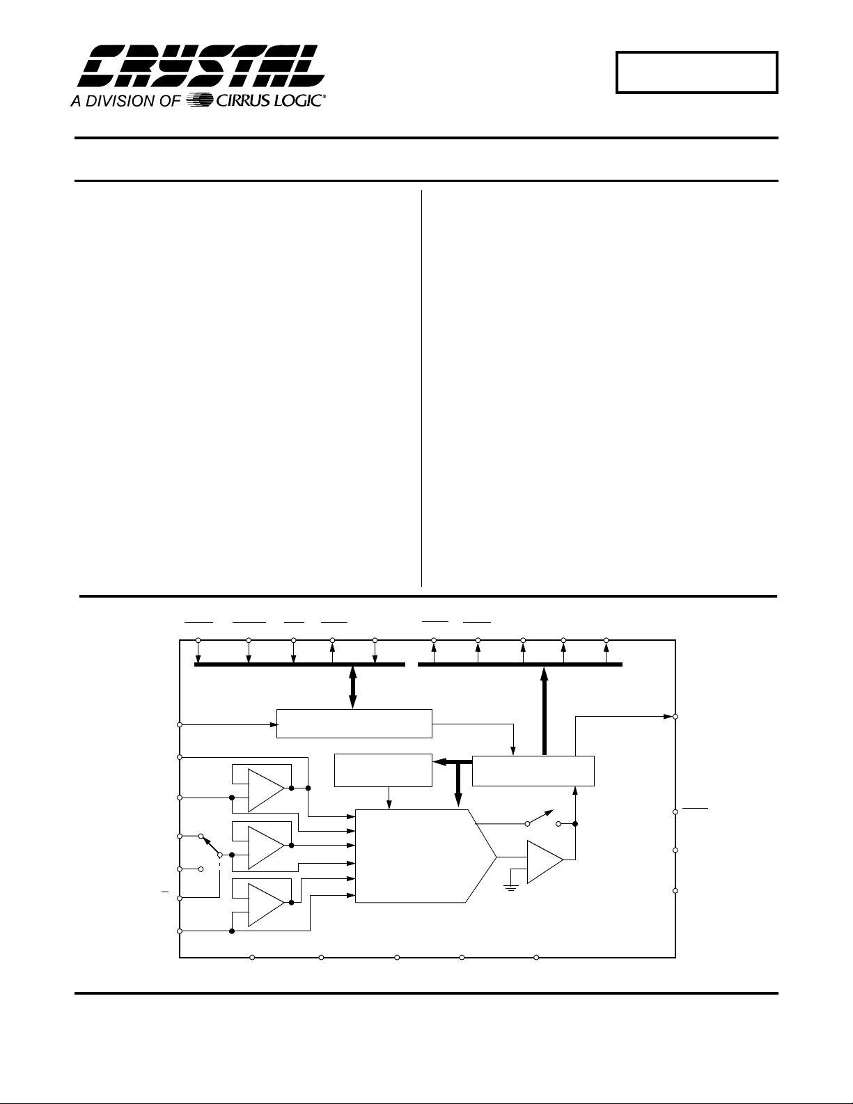
I
Description
The CS5126 CMOS analog-to-digital converter is an ideal front-end for stereo or monaural digital audio systems.
The CS5126 can be c onfigur ed to han dle two c hannels
at up to 50 kHz sam pling per channe l, or it can be co nfigured to sample one channel at rates up to 100 kHz.
The CS5126 executes a successive approximation algorithm using a charge redistribution architecture. On-chip
self-calibration ci rcui tr y h as 18- bi t re so lu tion thus av oi ding any degradation in performance with low-level
signals. The charge redistribution technique also provides an inherent sampling function which avoids the
need for external sample/hold amplifiers.
Signal-to-(noise+distortion) in stereo operation is 92 dB,
and is dominated by int ernal broad band nois e (1/2 LSB
rms). When the CS5126 is config ured for 2X oversampling, digital pos t-filtering bandlimits th is white noise to
20 kHz, increasing dynamic range to 95 dB.
ORDERING INFORMATION
CS5126-KP 0° to 70° C 28-pin Plastic DIP
CS5126-KL 0° to 70° C 28-pin PLCC
+2/' 6/((3 567 &2'(
$,1/
$,15
/5
&/.,1
5()%8)
95()
$*1'
Cirrus Logic, Inc.
Crystal Semiconductor Products Division
P.O. Box 17847, Austin, Texas 78760
(512) 445 7222 FAX: (512) 445 7581
http://www.crystal.com
67%<
&RQWURO
&DOLEUDWLRQ
65$0
%LW&KDUJH
5HGLVWULEXWLRQ
'*1' 9' 9'9$9$
75./
75.5
'$&
Copyright Cirrus Logic, Inc. 1997
(All Rights Reserved)
66+
66+
0LFURFRQWUROOHU
&RPSDUDWRU
6' $7$
6&/.
7(67
6&.02'
28702'
MAR ‘95
DS32F1
1
CS5126
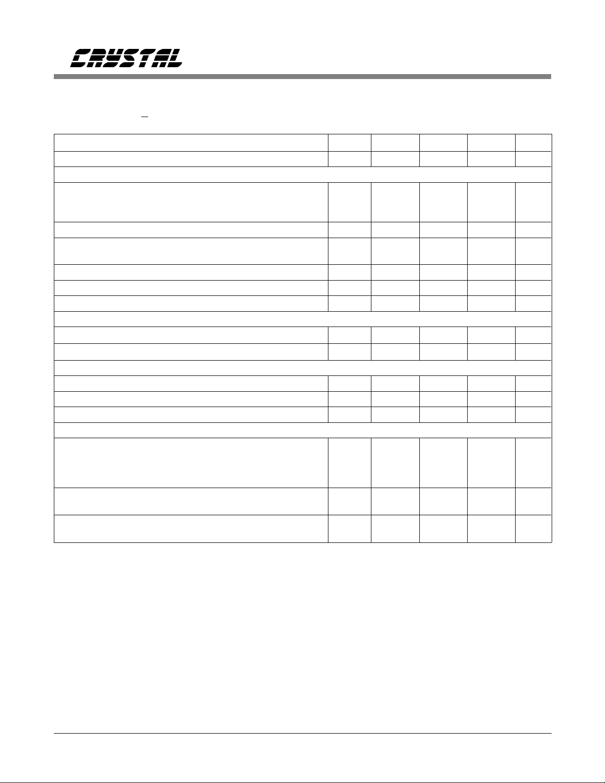
ANALOG CHARACTERISTICS
Full-Scale Input Sinewave, 1kHz; f
Stereo operation, L/
R toggling at 48 kHz unless otherwise specified.)
= 24.576MHz; VREF = 4.5V ; Analog Source Impedance = 200Ω;
clk
(TA = 25°C; VA+, VD+ = 5V; VA-, VD- = -5V;
Parameter* Symbol Min Typ Max Units
Resolution - - 16 Bits
Dynamic Performance
Signal-to-(Noise plus Distortion)
VIN = ±FS (10 Hz to 20 kHz)
VIN = -20dB (f = 20 kHz)
S/(N+D)
90
70
92
72
-
-
dB
dB
Total Harmonic Distortion THD - 0.001 - %
Dynamic Range Stereo Mode
Monaural (20 kHz BW)
Idle Channel Noise V
Interchannel Isolation (Note 1) I
Interchannel Mismatch M
DR 90
n(ic)
ic
ic
88 90 - dB
92
-
95
-
-
dB
dB
-1/2-LSB
-0.01-dB
dc Accuracy
Full-Scale Error FSE Bipolar Offset Error BPO -
±
4
±
4
-LSB
-LSB
Analog Input
Aperture Time t
Aperture Jitter t
Input Capacitance (Note 2) C
apt
ajt
in
-30-ns
- 100 - ps
- 200 - pF
Power Supplies
Power Supply Current Positive Analog (Note 3)
Negative Analog
(SLEEP High) Positive Digital
Negative Digital
Power Dissipation (SLEEP High) (Notes 3, 4)
(SLEEP Low)
Power Supply Rejection Positive S upplies (Note 5)
Negative Supplies
I
A+
I
A-
I
D+
I
D-
P
do
P
ds
PSR -
-
-
-
-
-
-
-
18
-18
8
-8
260
1
84
84
23
-23
12
-12
350
-
-
-
mA
mA
mA
mA
mW
mW
dB
dB
Notes: 1. One input grounded; dc to 20kHz, Full Scale input on the other channel.
Guaranteed by characterization.
2. Applies only in the track mode. When converting or calibrating, input capacitance will typically
be 10 pF.
3. All outputs unloaded. All inputs CMOS levels .
4. Power dissipation in sleep mode applies with no master clock applied (CLKIN high or low).
5. With 300mV p-p, 1kHz ripple applied to each supply separately. A plot of typical power supply
rejection appears in the
Analog Circuit Connections
section.
rms
* Refer to
Parameter Definitions
at the end of this data sheet.
Specifications are subject to change without notice.
2 DS32F1
CS5126
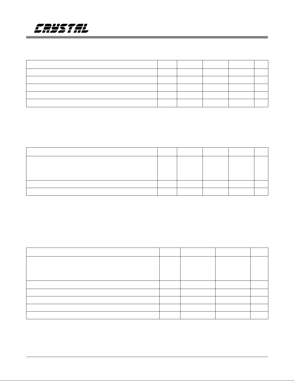
DIGITAL CHARACTERISTICS
(TA = T
MIN
to T
; VA+, VD+ = 5V±10%; VA-,VD - = -5V±10%)
MAX
Parameter Symbol Min Typ Max Units
High-Level Input Voltage V
Low-Level Input Voltage V
High-Level Output Voltage (Note 6) V
Low-Level Output Voltage I
= 1.6 mA V
out
Input Leakage Current I
Notes: 6. I
= -100 µA. This specification guarantees that each digital output will drive one TTL load
OUT
(V
= 2.4V @ I
OH
= -40 µA).
OUT
IH
IL
OH
OL
in
2.0 - - V
--0.8V
(VD+)-1.0V - - V
--0.4V
--10
RECOMMENDED OPERATING CONDITIONS (AGND, DGND = 0V, see note 7.)
Parameter Symbol Min Typ Max Units
DC Power Supplies: Positive Digital
Negative Digital
Positive Analog
Negative Analog
Analog Reference Voltage VREF 2.5 4.5 (VA+)-0.5 V
Analog Input Voltage (Note 8) V
Notes: 7. All voltages with respect to ground.
8. The CS5126 can accept input voltages up to the analog supplies (VA+, VA-). It will produce an
output of all 1’s for inputs above VREF and all 0’s for inputs below -VREF.
VD+
VD-
VA+
VA-
AIN
4.5
-4.5
4.5
-4.5
5.0
-5.0
5.0
-5.0
VA+
-5.5
5.5
-5.5
-VREF - VREF V
µ
A
V
V
V
V
ABSOLUTE MAXIMUM RATINGS (AGND, DGND = 0V, all voltages with respect to ground.)
Parameter Symbol Min Max Units
DC Power Supplies: Positive Digital
Negative Digital
Positive Analog
Negative Analog
Input Current, Any Pin Except Supplies (Note 9) I
Analog Input Voltage (AIN and VREF pins) V
Digital Input Voltage V
Ambient Temperature (power applied) T
Storage Temperature T
Notes: 9. Transient currents of up to 100 mA will not cause SCR latch-up.
WARNING: Operation at or beyond these limits may result in permanent damage to the device.
Normal operation is not guaranteed at these extremes.
DS32F1 3
VD+
VD-
VA+
VA-
in
INA
IND
A
stg
-0.3
0.3
-0.3
0.3
-
(VA+)+0.3
-6.0
6.0
-6.0
±10
mA
(VA-)-0.3 (VA+)+0.3 V
-0.3 (VD+)+0.3 V
-55 125 °C
-65 150 °C
V
V
V
V
CS5126
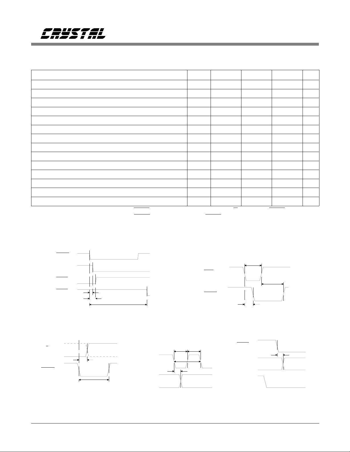
SWITCHING CHARACTERISTICS
Inputs: Logic 0 = 0V, Logic 1 = VD+; C
= 50 pF)
L
(TA = 25 °C; VA+, VD+ = 5V ± 10%; VA-, VD- = -5V ± 10%;
Parameter Symbol Min Typ Max Units
Master Clock Period t
HOLD to SSH2 Falling (Note 10) t
HOLD to TRKL, TRKR SSH1 Falling t
HOLD to TRKL, TRKR SSH1, SSH2 Rising t
RST Pulse Width t
RST to STBY Falling t
RST Rising to STBY Rising t
HOLD Pulse Width t
HOLD to L/R Edge (Note 10) t
SCLK period t
SCLK Pulse Width Low t
SCLK Pulse Width High t
SCLK Falling to SDATA Valid t
HOLD Falling to SDATA Valid t
Notes: 10. SSH2 only works correctly if
occurs between 30ns before
HOLD falling edge is within ±30ns of L/R edge OR if HOLD falling edge
HOLD rises to 192 t
clk
clk
dfsh2
dfsh1
drsh
rst
drrs
cal
hold
dhlri
sclk
sclkl
sclkh
dss
dhs
40 - - ns
-80-ns
198t
clk
-80-ns
150 - - ns
- 100 - ns
- 34,584,480 - t
2t
+50 - 192t
clk
-30 - 192t
200 - - ns
50 - - ns
50 - - ns
- 100 140 ns
- 140 200 ns
after HOLD falls.
- 214t
+50 ns
clk
clk
clk
clk
ns
ns
HOLD (i)
SSH2 (o)
TRKL (o)
TRKR (o)
Control Output Timing
L/R
HOLD
t
hold
Channel Selection Timing
t
dhlri
t
dfsh2
t
drsh
t
dfsh1
SCLK
SDATA
Serial Data Timing
t
dss
t
sclkl
t
sclkh
t
rst
RST
STBY
t
drrs
Reset and Calibration Timing
HOLD
t
sclk
SDATA
SCLK
Data Transmit Start Timing
t
t
cal
dhs
MSB
4 DS32F1

CS5126
GENERAL DESCRIPTION
The CS5126 is a 2-channel, 100kHz A/D converter designed specifically for stereo digital
audio. The device includes an inherent sample/hold and an on-chip analog switch for stereo
operation. Both left and right channels can thus
be sampled and converted at rates up to 50kHz
per channel. Alternatively, the CS5126 can be
implemented in 2X oversampling schemes for
improved dynamic range and distortion.
Output data is available in serial form with
either binary or 2’s complement coding. Control
outputs are also supplied for use with an external
sample/hold amplifier to implement simultaneous sampling.
THEORY OF OPERATION
The CS5126 implements a standard successive
approximation algorithm using a charge-redistribution architecture. Instead of the traditional resistor network, the DAC is an array of binaryweighted capacitors. When not converting, the
CS5126 tracks the analog input signal. The input
voltage is applied across each leg of the DAC
capacitor array, thus performing a voltage-tocharge conversion.
When the conversion command is issued, the
charge is trapped on the capacitor array and the
analog input is thereafter ignored. In effect, the
entire DAC capacitor array serves as analog
memory during conversion much like a hold capacitor in a sample/hold amplifier.
The conversion consists of manipulating the binary-weighted legs of the capacitor array to the
voltage reference and analog ground. All legs
share one common node at the input to the converter’s comparator. This forms a binaryweighted capacitive divider. Since the charge at
the comparator’s input remains fixed, the voltage
at that point depends on the proportion of capacitance tied to VREF versus AGND. The suc-
cessive-approximation algorithm is used to find
the proportion of capacitance which will drive
the voltage to the comparator’s trip point. That
binary fraction of capacitance represents the converter’s digital output.
Calibration
The ability of the CS5126 to convert accurately
clearly depends on the accuracy of its DAC. The
CS5126 uses an on-chip self-calibration scheme
to insure low distortion and excellent dynamic
range independent of input signal conditions.
Each binary-weighted bit capacitor actually consists of several capacitors which can be manipulated to adjust the overall bit weight. During
calibration, an on-chip microcontroller manipulates the sub-arrays to precisely ratio the bits.
Each bit is adjusted to just balance the sum of
all less significant bits plus one dummy LSB
(for example, 16C = 8C + 4C + 2C + C + C).
The result is typical differential nonlinearity of
±1/4 LSB. That is, codes typically range from
3/4 to 5/4 LSB’s wide.
The CS5126 should be reset upon power-up,
thus initiating a calibration cycle which takes 1.4
seconds to complete. The CS5126 then stores its
calibration coefficients in on-chip SRAM, and
can be recalibrated at any later time.
SYSTEM DESIGN WITH THE CS5126
All timing and control inputs to the CS5126 can
be easily generated from a master system clock.
The CS5126 outputs serial data and a variety of
digital outputs which can be used to control an
external sample/hold amplifier for simultaneous
sampling. The actual circuit connections depend
on the system architecture (stereo or monaural
2X oversampling), and on the sampling characteristics (simultaneous or sequential sampling
between channels).
DS32F1 5
CS5126
System Initialization
Upon power up, the CS5126 must be reset to
guarantee a consistent starting condition and in-
itially calibrate the device. Due to the CS5126’s
low power dissipation and low temperature drift,
no warm-up time is required before reset to accommodate any self-heating effects. However,
the voltage reference input should have stabilized to within 0.25% of its final value before
RST rises to guarantee an accurate calibration.
Later, the CS5126 may be reset at any time to
initiate a single full calibration. Reset overrides
all other functions. If reset, the CS5126 will
clear and initiate a new calibration cycle midconversion or midcalibration.
When RST is brought low all internal logic
clears. When it returns high a calibration cycle
begins which takes 34,584,480 master clock cycles to complete (approximately 1.4 seconds
with a standard 24MHz master clock). The
CS5126’s STBY output remains low throughout
the calibration sequence, and a rising transition
indicates the device is ready for normal operation.
A simple power-on reset circuit can be built using a resistor and capacitor as shown in Figure 1. The RC time constant must be long
enough to guarantee the rest of the system is
fully powered up and stable by the end of reset.
+5V
R
C
Figure 1. Power-On Reset Circuit
CS5126
RST
Master Clock
The CS5126 operates from an externally-supplied master clock. In stereo operation, the master clock frequency is set at 512 times the perchannel sampling rate (256 in 2X oversampling
schemes). The CS5126 can accept master clocks
up to 24.576 MHz for 48kHz stereo sampling or
96kHz monaural oversampling.
All timing and control inputs for channel selection, sampling, and serial data transmission may
be divided down from the master clock. This
yields a completely synchronous system, avoiding sampling and conversion errors due to asynchronous digital noise.
CIRCUIT CONNECTIONS
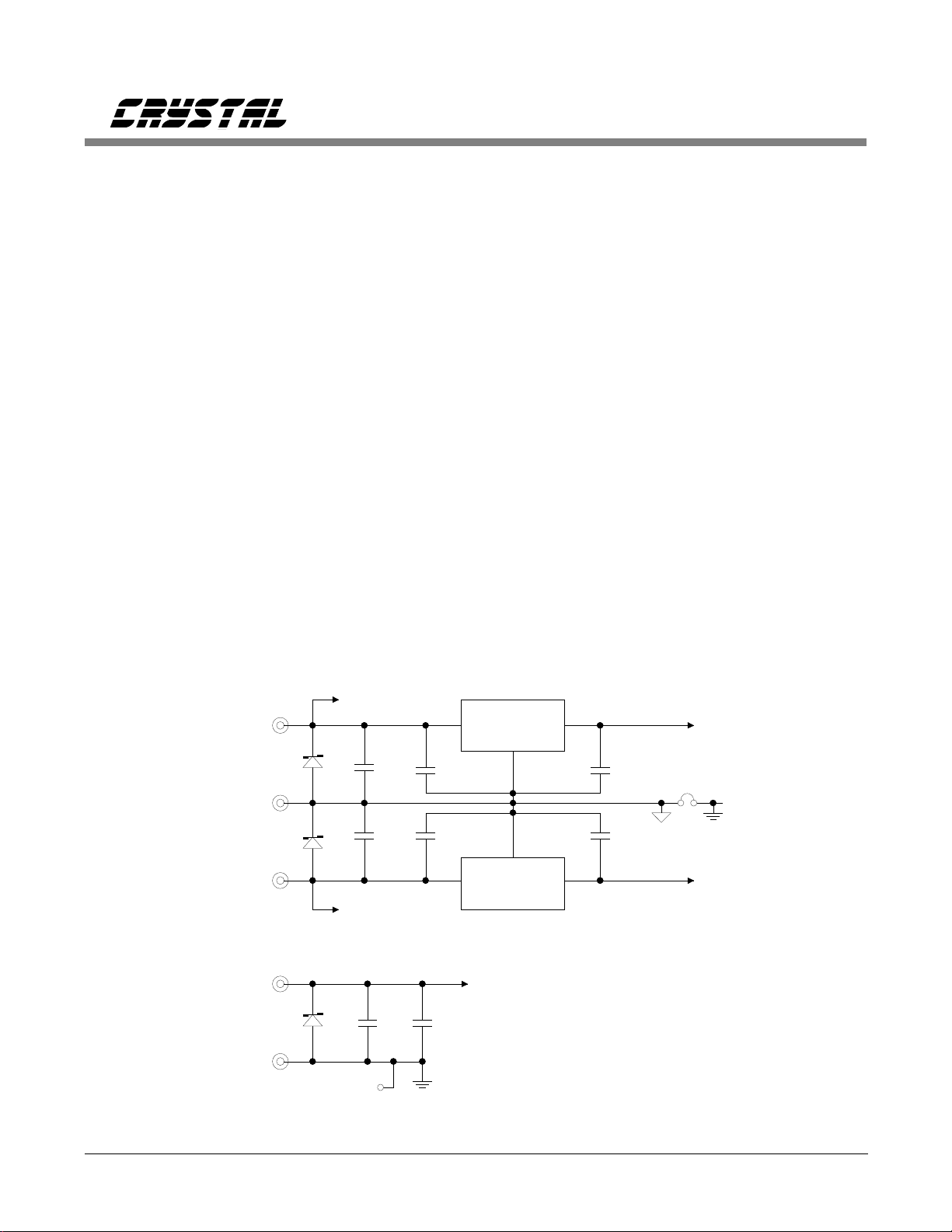
Stereo Operation
Figure 2 shows the standard circuit connections
for operating the CS5126 in its stereo mode. The
HOLD, L/R, and SCLK inputs are derived from
the master clock using a binary divider string. A
24.576 MHz master clock is required for a sampling rate of 48kHz per channel.
For 48kHz stereo sampling, the CS5126 must
sample and convert at a 96kHz rate to handle
both channels. The master clock is divided by
256 and applied to the HOLD input. A falling
transition on the HOLD pin places the input in
the hold mode and initiates a conversion cycle.
The HOLD input is latched internally by the
master clock, so it can return high anytime after
one master clock cycle plus 50ns.
In stereo operation the CS5126 alternately samples and converts the left and right input channels. This alternating channel selection is
achieved by dividing the HOLD input by two
(that is, dividing the master clock by 512) and
applying it to the L/R input. Upon completion of
each conversion cycle, the CS5126 automatically
returns to the track mode. The status of L/R as
6 DS32F1
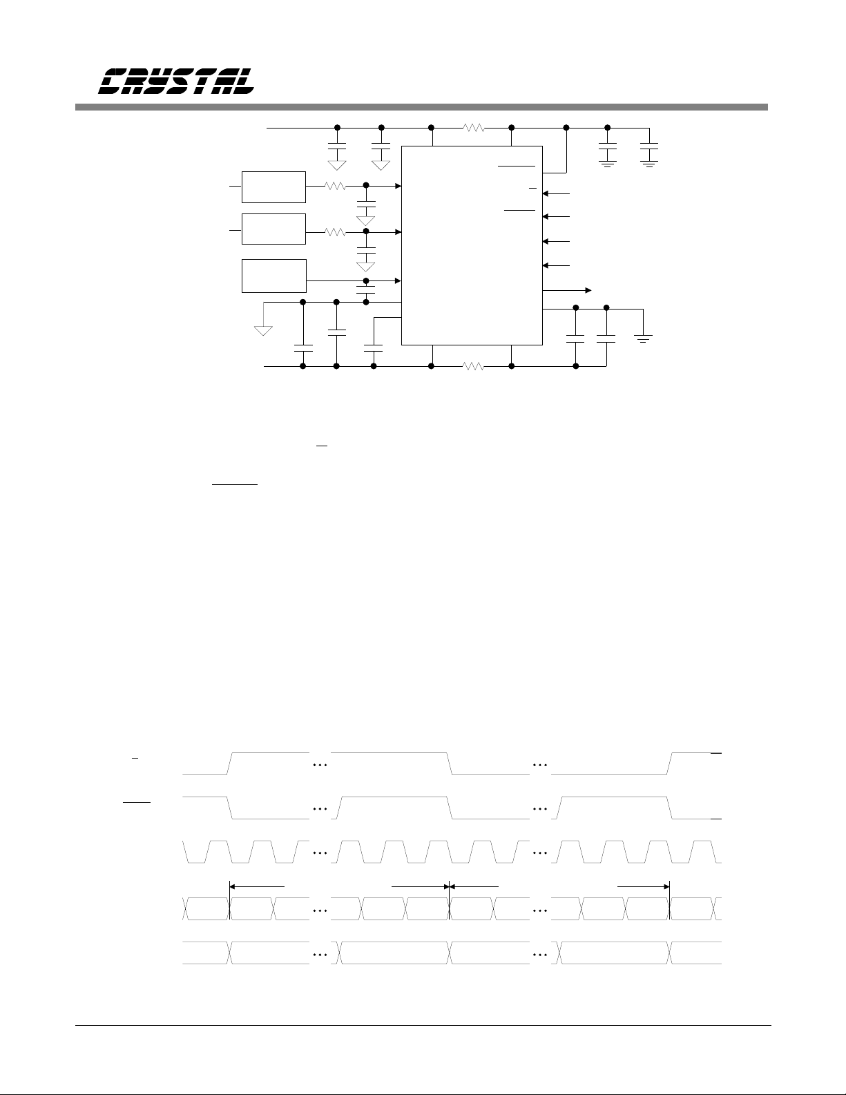
CS5126
Left Ch.
Analog In
Right Ch.
Analog In
+5V
Anti Alias
Filter
Anti Alias
Filter
Voltage
Reference
-5V
1 µF
+
+
200
1 nF
200
1 nF
1
Ω
Ω
0.1
µ
F
0.1µF
µ
F
0.1
Figure 2. Stereo Mode Connection Diagram
each conversion finishes determines which channel is acquired and tracked. The L/R input must
remain valid at least until 30ns before the next
falling transition on HOLD.
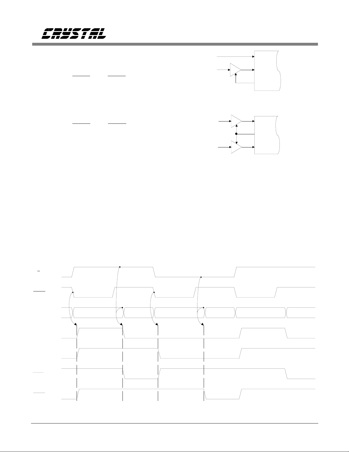
As shown in the timing diagram in Figure 3, the
CS5126 uses pipelined data transmission. That
is, data from a particular conversion transmits
during the next conversion cycle. The serial
clock input, SCLK, is derived by dividing the
master clock by 16. The MSB (most-significantbit) will be stable on the first rising edge of
SCLK after a falling transition on HOLD. With
a serial clock of f
/16, transmission of all 16
clk
output bits will span an entire conversion and
acquisition cycle.
VA+
AINL
AINR
VREF
AGND
REFBUF
VA-
µ
F
10
CS5126
10
Ω
Ω
VD+
SLEEP
L/R
HOLD
SCLK
CLKIN
SDATA
DGND
VD-
0.1
0.1
f /512
clk
f /256
clk
f /16
clk
f
clk
F
µ
µ
F
1 µF
+
+
1 µF
STEREO MODE PERFORMANCE
As illustrated in Figure 4, the CS5126 typically
provides 92dB S/(N+D) and 0.001% THD. Unlike conventional successive-approximation
ADC’s, the CS5126’s signal-to-noise and dynamic range are not limited by differential nonlinearities (DNL) caused by calibration errors.
Rather, the dominant noise source is broadband
thermal noise which aliases into the baseband.
This white broadband noise also appears as an
idle channel noise of 1/2 LSB (rms).
L/R (i)
HOLD (i)
SCLK (i)
Right Channel DataLeft Channel Data
SDATA (o)
Internal
Status
LSB MSB LSB MSB LSB MSB
Rch Conv. Lch Conv. Rch Acq.Lch Acq.
Figure 3. Stereo Mode Timing
DS32F1 7
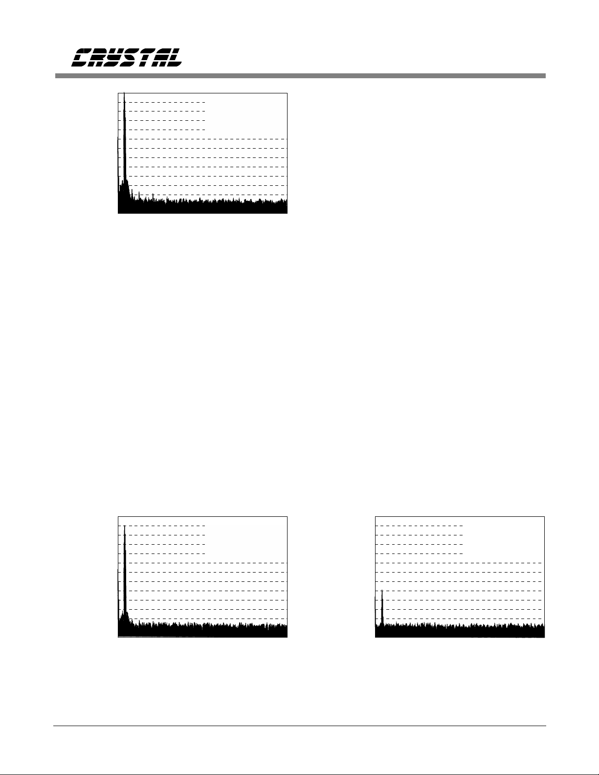
CS5126
Signal
Amplitude
Relative to
Full Scale
0dB
-20dB
-40dB
-60dB
-80dB
-100dB
-120dB
1 kHz
Input Frequency
Sampling Rate: 48 kHz
Full Scale: 9V p-p
S/(N+D): 91.75 dB
S/(N+D): 92.53 dB
(dc to 20 kHz)
24kHz
Figure 4. FFT Plot of CS5126 in Stereo Mode
(Left Channel with 1 kHz, Full-Scale Input)
Differential Nonlinearity
The self-calibration scheme utilized in the
CS5126 features a calibration resolution of 1/4
LSB, or 18-bits. This ideally yields DNL of
±1/4 LSB, with code widths ranging from 3/4 to
5/4 LSB’s. This insures consistent sound quality
independent of signal level.
Traditional laser trimmed ADC’s have significant differential nonlinearities which are disastrous to sound quality with low-level signals.
Appearing as wide and narrow codes, DNL
often causes entire sections of the transfer func-
tion to be missing. Although their affect is minor
on S/(N+D) with high amplitude signals, DNL
errors dominate performance with low-level signals. For instance, a signal 80dB below fullscale will slew past only 6 or 7 codes. Half of
those codes could be missing with a conventional hybrid ADC capable of only 14-bit DNL.
The most common source of DNL errors in conventional ADC’s is bit weight errors. These can
arise due to accuracy limitations in factory trim
stations, thermal or physical stresses after calibration, and/or drifts due to aging or temperature
variations in the field. Bit-weight errors have a
drastic effect on a converter’s ac performance.
They can be analyzed as step functions superimposed on the input signal. Since bits (and their
errors) switch in and out throughout the transfer
curve, their effect is signal dependent. That is,
harmonic and intermodulation distortion, as well
as noise, can vary with different input conditions.
Differential nonlinearities in successive-approximation ADC’s also arise due to dynamic errors
in the comparator. Such errors can dominate if
the converter’s throughput/sampling rate is
driven too high. The comparator will not be allowed sufficient time to settle during each bit
decision in the successive-approximation algo-
Signal
Amplitude
Relative to
Full Scale
0dB
-20dB
-40dB
-60dB
-80dB
-100dB
-120dB
1 kHz
Input Frequency
Sampling Rate: 48 kHz
Full Scale: 9V p-p
S/(N+D): 83.27 dB
S/(N+D): 84.06 dB
(dc to 20 kHz)
a. Left Channel with 1 kHz, -10 dB Input
24kHz
Signal
Amplitude
Relative to
Full Scale
0dB
-20dB
-40dB
-60dB
-80dB
-100dB
-120dB
1 kHz
Input Frequency
Sampling Rate: 48 kHz
Full Scale: 9V p-p
S/(N+D): 13.70 dB
S/(N+D): 14.49 dB
(dc to 20 kHz)
b. Left Channel with 1 kHz, -80 dB Input
24kHz
Figure 5. FFT Plots of CS5126 in Stereo Mode
8 DS32F1
CS5126
rithm. The worst-case codes for dynamic errors
are the major transitions (1/2 FS; 1/4, 3/4 FS;
etc.). Since DNL effects are most critical with
low-level signals, the codes around in mid-scale,
(that is, 1/2 FS), are most important. Yet those
codes are worst-case for dynamic DNL errors!
With all linearity calibration performed on-chip
to 18-bits, the CS5126 maintains accurate bit
weights. DNL errors are dominated by residual
calibration errors of ±1/4 LSB rather than dynamic errors in the comparator. Furthermore, all
DNL effects on S/(N+D) are buried by white
broadband noise. This yields excellent sound
quality independent of signal level.
(See Figure 5)
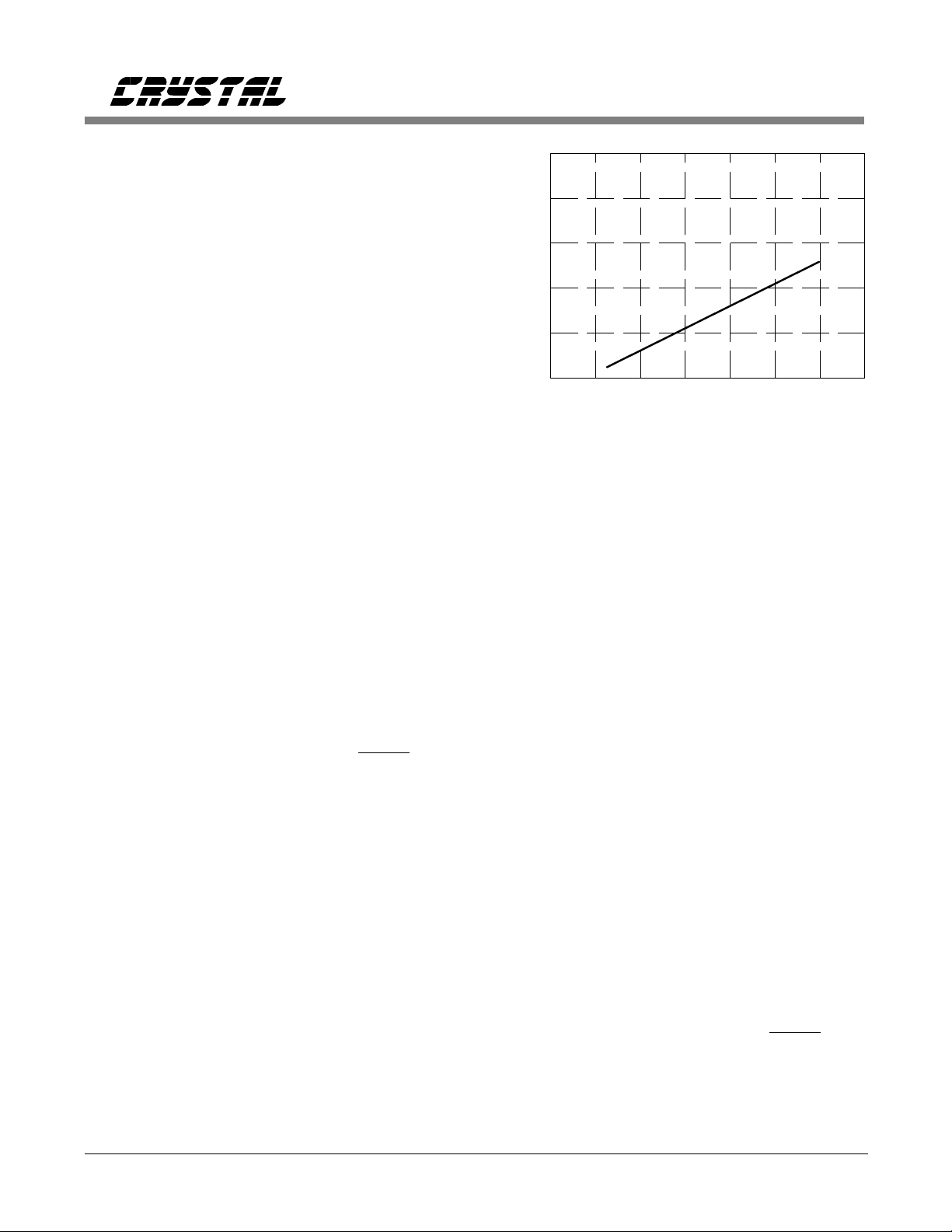
Sampling Distortion
Like most discrete sample/hold amplifier de-
signs, the CS5126’s inherent sample/hold exhibits a frequency-dependent distortion due to
nonideal sampling of the analog input voltage.
The calibrated capacitor array used during conversions is also used to track and hold the analog input signal. The conversion is not performed on the analog input voltage per se, but is
actually performed on the charge trapped on the
capacitor array at the moment the HOLD command is given. The charge on the array ideally
assumes a linear relationship to the analog input
voltage. Any deviation from this linear relationship will result in conversion errors even if the
conversion process proceeds flawlessly.
At dc, the DAC capacitor array’s voltage coefficient dictates the converter’s linearity. This variation in capacitance with respect to applied signal voltage yields a nonlinear relationship between the charge on the array and the analog input voltage and places a bow or wave in the
transfer function. This is the dominant source of
distortion at low input frequencies (Figure 4).
0.020
0.016
0.012
THD (%)
0.008
0.004
0
Figure 6. THD vs Input Frequency
5kHz 10kHz 15kHz 20kHz 25kHz
Analog Input Frequency
( 9V p-p Full-Scale Input)
The ideal relationship between the charge on the
array and the input voltage can also be distorted
at high signal frequencies due to nonlinearities
in the internal MOS switches. Dynamic signals
cause ac current to flow through the switches
connecting the capacitor array to the analog input pin in the track mode. Nonlinear on-resistance in the switches causes a nonlinear voltage
drop. This effect worsens with increased signal
frequency and slew rate as shown in Figure 6
since the magnitude of the steady state current
increases. First noticeable at 1kHz, this distortion assumes a linear relationship with input frequency. With signals 20dB or more below full-
scale, it no longer dominates the converter’s
overall S/(N+D) performance.
This distortion is strictly an ac sampling phenomenon. If significant energy exists at high frequencies, the effect can be eliminated using an
external track-and-hold amplifier to allow the ar-
ray’s charge current to decay, thereby eliminating any voltage drop across the switches. Since
the CS5126 has a second sampling function onchip, the external track-and-hold can return to
the track mode once the converter’s HOLD input
falls. It need only acquire the analog input by
the time the entire conversion cycle finishes.
DS32F1 9
CS5126
Simultaneous Sampling
The CS5126 offers four digital output signals,
SSH1, SSH2, TRKL, and TRKR which can be
used to control external sample/hold amplifiers
to achieve simultaneous sampling and/or reduce
sampling distortion.
Figure 7 shows the timing relationships for
SSH1, SSH2, TRKL, and TRKR. In the stereo
configuration shown in Figure 1 the CS5126
samples the left and right channels 180° out of
phase. Simultaneous sampling between the left
and right channels can be achieved as shown in
Figure 8a using the CS5126’s SSH2 output. The
external sample/hold will freeze the right channel analog signal as the CS5126 freezes the left
channel input at AINL. It will hold that signal
valid at AINR until the CS5126 begins a right
channel conversion. Once that conversion begins, the sample/hold returns to the sample
mode. The acquisition time for the external sample/hold amplifier must not exceed the CS5126’s
minimum conversion time of 192 master clock
cycles (7.8µs for 48kHz stereo sampling).
AINL
S/H
AINR
SSH2
a. Standard Connections
S/H
AINL
SSH1
S/H
AINR
b. High-Slew Conditions
Figure 8. Simultaneous Sampling Connections
The CS5126’s sampling distortion with high-frequency, high-amplitude input signals may be improved if a low distortion sample/hold amplifier
is used as shown in Figure 8a. The right channel
input at AINR will appear as dc to the CS5126
resulting in no ac current flowing through the
internal MOS switches. Sampling distortion can
likewise be improved for both channels using
the SSH1 output as shown in Figure 8b. Simi-
L/R (i)
HOLD (i)
Internal
Status
SSH1 (o)
SSH2 (o)
TRKL (o)
TRKR (o)
10 DS32F1
Acq. & Track Hold
Acquire & Trac k Hold
Figure 7. External Sampling Control Output Timing
Lch Acq. Rch Acq. Rch Convert Lch Acq.Lch ConvertRch Convert

CS5126
Analog
Input
+5V
Anti Alias
Reference
-5V
+
1 µF
Filter
Voltage
200
0.1 µF
+
1 µF
Figure 9. Monaural 2X Oversampling Connections
0.1
1nF
Ω
0.1 µF
* AINR can alternatively be used
with L/R grounded
larly, the acquisition time for the external sample/hold amplifiers must not exceed the minimum conversion time of 192 master clock cycles
(7.8µs for 48kHz stereo sampling).
Oversampling
The CS5126 can alternatively be used to oversample one channel (monaural) by 2X simply by
tying the L/R input high or low. This moves
much of the anti-alias burden from analog filters
to digital post-filtering. The analog filters’ corner can be pushed out in frequency with lower
roll-off, allowing lower passband ripple and
more linear phase in the audioband. Digital FIR
filtering, meanwhile, can be used to implement
high roll-off filters with ultra-low passband ripple and perfectly linear phase.
µ
F
AINL*
AINR
VREF
AGND
REFBUF
10
CS5126
VA- VD-
10
sive-approximation ADC the noise spectral content is white. Therefore, in a 2X oversampling
scheme such as 96kHz sampling the ADC’s
noise will be be spread uniformly from dc to
48kHz. Digital post-filtering then rejects noise
outside of the 20kHz or 22kHz bandwidth, resulting in improved signal-to-noise and dynamic
range. For a white noise spectrum, a 2X reduction in bandwidth yields a 3dB improvement in
dynamic range.
Due to its on-chip self-calibration scheme, the
CS5126’s dynamic range is limited only by
white broadband noise rather than signal-dependent DNL errors. Therefore, the CS5126 picks up
a full 3dB improvement in dynamic range to
95dB when implemented in 2X oversampling
schemes.
Ω
Ω
VD+VA+
SLEEP
L/R
HOLD
SCLK
CLKIN
SDATA
DGND
0.1 µF
µ
0.1
+5V*
f /256
clk
f /16
clk
f
clk
F
+
1 µF
+
1 µF
Oversampling not only improves system-level
filtering performance, but it also enhances the
ADC’s dynamic range and distortion characteristics. All noise energy in a sampled, digital
signal aliases into the baseband between dc and
one-half the sampling rate. For an ideal succes-
Oversampling and digital filtering also enhance
the ADC’s distortion performance. Consider for
example a full-scale 15kHz input signal to the
CS5126 sampling at 96kHz. Sampling distortion
produces THD of approximately 0.005% (86dB)
at the converter’s output. Most of the distortion
energy resides in the second and third harmonics
DS32F1 11

Left Channel
Analog In
Right Channel
Analog In
Anti Alias
Filter
+5V
Anti Alias
Filter
CS5126
CLKIN
AINL
L/R
L/R
AINL
CS5126
SDATA
HOLD
SCLK
SCLK
HOLD
SDATA
CLKIN
DINL
IBO
IBCK
DINR
Digital Filter
CKIN
OBCK
WDCK
LRCK
DOL
SM5805
Figure 10. Example Oversampling System D iagram
512
f
s
256 f
s
32 f
s
2
f
s
f
s
DATA IN
System
CS5126
at 30kHz and 45kHz. Meanwhile, digital filters
such as the SM5805 shown in Figure 10 will
roll-off rapidly from 22kHz to 28kHz and reject
distortion energy in the second, third, and fourth
harmonics. Clearly, oversampling results in superior system-level distortion.
Still, if the CS5126’s distortion performance
with high-frequency, high-amplitude signals
must be enhanced in 2X oversampling schemes,
the TRKL or TRKR outputs can be used. Either
TRKL or TRKR will fall at the end of each conversion cycle depending on which channel is being acquired. The AINL and TRKL connections
(or AINR and TRKR) can be used as shown in
Figure 11 to control an external low-distortion
sample/hold to create an effective dc input for
the CS5126 and remove sampling distortion.
Digital Circuit C onnections
When TTL loads are utilized the potential for
crosstalk between digital and analog sections of
the system is increased. This crosstalk is due to
high digital supply and signal currents arising
from the TTL drive current required of each
digital output. Connecting CMOS logic to the
digital outputs is recommended. Suitable logic
families include 4000B, 74HC, 74AC, 74ACT,
and 74HCT.
The CS5126 has a power down mode, initiated
by bringing SLEEP low. During power down,
the A/D Converter’s calibration information is
retained. The CS5126 may be used for conversion immediately after SLEEP is brought high.
Left
Analog In
+5V
Figure 11. High-Slew Monaural Connections
0dB
-20dB
-40dB
-60dB
Signal
Amplitude
Relative to
Full Scale
-80dB
-100dB
-120dB
1 kHz
Figure 12. FFT Plot of CS5126 in Monaural 2X Over-
S/H
AINL
TRKL
L/R
Input Frequency
sampling Mode
Sampling Rate: 96 kHz
Full Scale: 9V p-p
S/(N+D): 91.44 dB
S/(N+D): 95.25 dB
(dc to 20 kHz)
48kHz
12 DS32F1

CS5126
ANALOG CIRCUIT CONNECTIONS
Most popular successive-approximation A/D
converters generate dynamic loads at their analog connections. The CS5126 internally buffers
all analog inputs (AIN, VREF, and AGND) to
ease the demands placed on external circuitry.
However, accurate system operation still requires
careful attention to details at the design stage regarding source impedances as well as grounding
and decoupling schemes.
Reference Considerations
An application note titled "Voltage references
for the CS501X/CSZ511X Series of A/D Converters" is available which describes the dynamic
load conditions presented by the VREF input on
Crystal’s self-calibrating SAR A/D converters
(including the CS5126). As the CS5126 sequences through bit decisions it switches portions of the capacitor array to the VREF pin in
accordance with the successive-approximation
algorithm. For proper operation, the source impedance at the VREF pin must remain low at
frequencies up to 1MHz.
A large capacitor connected between VREF and
AGND can provide sufficiently low output impedance at the frequencies of interest, so the reference voltage can simply be derived as shown
in Figure 13a. Although very low cost, this reference has almost no power supply rejection
from the VA+ line.
Alternatively, a more stable and precise reference can be generated using a TL431 shunt reference from T.I. or Motorola, as shown in Figure 13b.
The magnitude of the current load on the external reference circuitry will scale to the master
clock frequency. At the full-rated 24 MHz clock
the reference must supply a maximum load current of 20µA peak-to-peak (2µA typical). An
output impedance of 2Ω will therefore yield a
maximum error of 40m V. With a 4.5V reference
and LSB size of 138mV this would insure approximately 1/4 LSB accuracy. A 10µF capaci-
tor exhibits an impedance of less than 2Ω at frequencies greater than 16kHz. A high-quality tantalum capacitor in parallel with a smaller ceramic capacitor is recommended.
VA+
IN4148
10 k
DS32F1 13
100
Ω
Ω
+
a. Simple Reference
100 µF
VREF
0.1 µF
AGND
Figure 13. Sugg ested Volt age Referen ce Circuits
+12 or +15 V
TL431
2 k
Ω
50
Ω
0.1 µF
b. Low-cost Shunt Reference
1.6 k
2 k
VREF
Ω
+
10 µF
Ω
0.1 µF
AGND

CS512 6
The CS5126 can operate with a wide range of
reference voltages, but signal-to-noise performance is maximized by using as wide a signal
range as possible. The recommended reference
voltage is 4.5 volts. The CS5126 can actually
accept reference voltages up to the positive analog supply. However, as the reference voltage
approaches V A+ the external drive requirements
may increase at VREF.
An internal reference buffer is used to protect
the external reference from current transients
during conversion. This internal buffer enlists
the aid of an external 0.1µF ceramic capacitor
which must be tied between its output,
REFBUF, and the negative analog supply, V A-.
Analog Input Connection
Each time the CS5126 finishes a conversion cycle it switches the internal capacitor array to the
appropriate analog input pin, AINL or AINR.
This creates a minor dynamic load at the sampling frequency. All throughput specifications
apply for maximum analog source impedances
of 200Ω at AINL and AINR. In addition, the
comparator requires source impedances of less
than 400Ω around 2MHz for stability, which is
met by practically all bipolar op amps. For more
information, see our Application Note: "Input
Buffers for the CS501X/CSZ511X Series of A/D
Converters"
Analog Input Range/Coding Format
The CS5126 features a bipolar input range with
the reference voltage applied to VREF defining
both positive and negative full-scale. The coding
format is set by the state of the CODE input. If
high, coding is 2’s complement; if low, the
CS5126’s output is in offset-binary format.
Grounding and Power Supply Decoupling
The CS5126 uses the analog ground
connection, AGND, only as a reference voltage.
No dc power or signal currents flow through the
AGND connection, thus minimizing the potential
for interchannel crosstalk. Also, AGND is completely independent of DGND. However, any
noise riding on the AGND input relative to the
system’s analog ground will induce conversion
errors. Therefore, both analog inputs and the reference voltage should be referred to the AGND
pin, which should be used as the entire system’s
analog ground. The digital and analog supplies
are isolated within the CS5126 and are pinned
out separately to minimize coupling between the
analog and digital sections of the chip. All four
supplies should be decoupled to their respective
grounds using 0.1 µF ceramic capacitors. If sig-
nificant low frequency noise is present on the
supplies, 1 µF tantalum capacitors are recom-
mended in parallel with the 0.1 µF capacitors.
The positive digital power supply of the CS5126
must never exceed the positive analog supply by
more than a diode drop or the CS5126 could
experience permanent damage. If the two sup-
plies are derived from separate sources, care
must be taken that the analog supply comes up
first at power-up. The system connection diagrams in figures 2 and 9 show a decoupling
scheme which allows the CS5126 to be powered
from a single set of ± 5V rails. The positive
digital supply is derived from the analog supply
through a 10Ω resistor to avoid the analog supply dropping below the digital supply. If this
scheme is utilized, care must be taken to insure
that any digital load currents (which flow
through the 10 Ω resistors) do not cause the
magnitude of digital supplies to drop below the
analog supplies by more than 0.5 volts. Digital
14 DS32F1

CS5126
supplies must always remain above the minimum specification.
As with any high-precision A/D converter, the
CS5126 requires careful attention to grounding
and layout arrangements. However, no unique
layout issues must be addressed to properly apply the CS5126. The CDB5126 evaluation board
is available for the CS5126, which avoids the
need to design, build, and debug a high-precision PC board to initially characterize the part.
The board comes with a socketed CS5126, and
Schematic & Layout Review Service
Confirm Optimum
Confirm Optimum
Schematic & Layout
Schematic & Layout
Before Building Your Board.
Before Building Your Board.
For Our Free Review Service
For Our Free Review Service
Call Applications Engineering.
Call Applications Engineering.
can be quickly reconfigured to simulate any
combination of sampling and master clock conditions.
Power Supply Rejection
The CS5126 features a fully differential comparator design, resulting in superior power supply
rejection. Rejection is further enhanced by the
on-chip self-calibration and "auto-zero" process.
Figure 14 shows worst-case rejection for all
combinations of conversion rates and input con-
90
80
70
60
50
40
Power Supply Rejection (dB)
30
Call:(512) 445-7222
20
ditions.
1 kHz 10 kHz 100 kHz 1 MHz
Power Supply Ripple Frequency
Figure 14. Power Supply Rejection
DS32F1 15

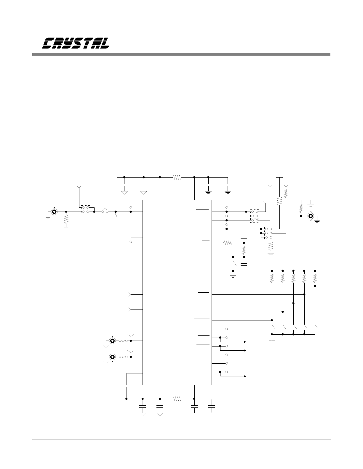
PIN DESCRIPTIONS
CS5126
NEGATIVE DIGITAL POWER VD- SLEEP SLEEP (LOW POWER) MODE
RESET & INITIATE CALIBRATION
RST TST4 TEST
MASTER CLOCK INPUT CLKIN
NO CONNECTION NC VA+ POSITIVE ANALOG POWER
STANDBY (CALIBRATING)
STBY AINR RIGHT CHANNEL ANALOG INPUT
DIGITAL GROUND DGND VA- NEGATIVE ANAL OG POWER
POSITIVE DIGITAL POWER VD+ AGND ANALOG GROUND
TRACKING LEFT CHANNEL
TRACKING RIGHT CHANNEL
TRKL REFBUF REFERENCE BUFFER
TRKR VREF VOLTAGE REFERENCE
SIMULTANEOUS SAMPLE/HOLD 1 SSH1 AINL LEFT CHANNEL ANALOG INPUT
SIMULTANEOUS SAMPLE/HOLD 2 SSH2
HOLD & CONVERT
LEFT/RIGHT CHANNEL SELECT L/
HOLD TST1 TEST
RCODEBINARY/2’s COMPLEMENT SELECT
SERIAL DATA CLOCK SCLK SDATA SERIAL DATA OUTPUT
1
2
3
4
5
6
7
8
9
10
11
12
13
14
28
27
26
TST3 TEST
25
24
23
22
21
20
19
18
TST2 TEST
17
16
15
NEGATIVE DIGITAL POWER VD-
RESET & INITIATE CALIBRATION
RST SLEEP SL EEP (LOW POWER) MODE
MASTER CLOCK INPUT CLKIN
NO CONNECTION NC
STANDBY (CALIBRATING)
DIGITAL GROUND DGND AINR RIGHT CHANNEL ANALOG INPUT
POSITIVE DIGITAL POWER VD+ VA- NEGATIVE ANALOG POWER
TRACKING LEFT CHANNEL
TRACKING RIGHT CHANNEL
SIMULTANEOUS SAMPLE/HOLD 1 SSH1 VREF VOLTAGE REFERENCE
STBY VA+ POSITIVE ANALOG POWER
3272426281
5
6
7
TRKL AGND ANALOG GROUND
TRKR REFBUF REFERENCE BUFFER
8
9
10
11
12 14 16 1813 15 17
top
view
25
24
23
22
21
20
19
TST4 TEST
TST3 TEST
SIMULTANEOUS SAMPLE/HOLD 2 SSH2 AINL LEFT CHANNEL ANALOG INPUT
HOLD & CONVERT
LEFT/RIGHT CHANNEL SELECT L/
HOLD TST2 TEST
R TST1 TEST
SERIAL DATA CLOCK SCLK CODE BINARY/2’s COMPLEMENT SELECT
SDATA SERIAL DATA OUTPUT
16 DS32F1

Power Supply Connections
VD+ - Positive Digital Power, PIN 7.
Positive digital power supply. Nominally +5 volts.
VD- - Negative Digital Power, PIN 1.
Negative digital power supply. Nominally -5 volts.
DGND - Digital Ground, PIN 6.
Digital ground reference.
VA+ - Positive Analog Power, PIN 25.
Positive analog power supply. Nominally +5 volts.
VA- - Negative Analog Power, PIN 23.
Negative analog power supply. Nominally -5 volts.
AGND - Analog Ground, PIN 22.
Analog ground reference.
Oscillator
CS5126
CLKIN - Clock Input, PIN 3.
All conversions and calibrations are timed from a master clock which must be externally
supplied.
Digital Inputs
HOLD - Hold, PIN 12.
A falling transition on this pin sets the CS5126 to the hold state and initiates a conversion. This
input must remain low at least one master clock cycle plus 50ns.
L/R - Left/Right Input Channel Select, PIN 13.
Status at the end of a conversion cycle determines which analog input channel will be acquired
for the next conversion cycle.
SLEEP - Sleep, PIN 28.
When brought low causes the CS5126 to enter a low-power quiescent state. All calibration
coefficients are retained in memory, so no recalibration is needed after returning to the normal
operating mode.
CODE - 2’s Complement/Binary Coding Select, PIN 16.
Determines whether data appears in 2’s complement or offset-binary format. If high, 2’s
complement; if low, offset-binary.
SCLK - Serial Clock, PIN 14.
Serial data changes status on a falling edge of this input, and is valid on a rising edge.
DS32F1 17

RST - Reset, PIN 32.
When taken low, all internal digital logic is reset. Upon returning high, a full calibration
sequence is initiated which takes 34,584,480 master clock cycles to complete.
Analog Inputs
AINL, AINR - Left and Right Channel Analog Inputs, PINS 19 and 24.
Analog input connections for the left and right input channels.
VREF - Voltage Reference, PIN 20.
The analog reference voltage which sets the analog input range. Its magnitude sets both positive
and negative full-scale.
Digital Outputs
STBY - Standby (Calibrating), PIN 5.
Indicates calibration status after reset. Remains low throughout the calibration sequence and
returns high upon completion.
SDATA - Serial Output, PIN 15.
Presents each output data bit on a falling edge of the SCLK input. Data is valid to be latched
on the rising edge of SCLK.
CS5126
SSH1, SSH2 - Simultaneous Sample/Hold 1 and 2, PINS 10 and 11.
Used to control external sample/hold amplifier(s) to achieve simultaneous stereo sampling.
TRKL, TRKR - Tracking Left, Tracking Right, PINS 8 and 9.
Indicate the end of a conversion cycle. Either TRKL or TRKR falls at the end of a conversion
cycle depending on the status of L/R and which channel is to be tracked.
Analog Outputs
REFBUF - Reference Buffer Output, PIN 21.
Reference buffer output. A 0.1µF ceramic capacitor must be tied between thi s pin and VA-.
Miscellaneous
NC - No Connection, PIN 4.
Must be left floating for proper operation.
TST1, TST2, TST3, TST4 - Test, PINS 17, 18, 26, 27.
Allow access to the CS5126’s test functions which are reserved for factory use. Must be tied to
VD+.
18 DS32F1

CS5126
PARAMETER DEFINITIONS
Total Harmonic Distortion - The ratio of the rms sum of all harmonics up to 20 kHz to the rms
value of the signal. Units in percent.
Signal-to-Noise plus Distortion Ratio - The ratio of the rms value of the signal to the rms sum of all
other spectral components below the Nyquist rate (excepting dc), including distortion components. Expressed in decibels.
Dynamic Range - Full-scale Signal-to-Noise plus Distortion with the input signal 60dB below fullscale. Units in decibels.
Interchannel Isolation - A measure of crosstalk between the left and right channels. Measured for
each channel at the converter’s output with the input under test grounded and a full-scale signal applied to the other channel. Units in decibels.
Full Scale Error - The deviation of the last code transition from the ideal (VREF-3/2 LSB’s) after all
offsets have been externally compensated. Units in decibels relative to full scale.
Bipolar Offset - The deviation of the mid-scale transition (011...111 to 100...000) from the ideal
(1/2 LSB below AGND). Units in microvolts.
Interchannel Mismatch - The difference in output codes between the left and right channels with the
same analog input applied. Units expressed in decibels relative to full scale. Tested at full scale input.
Aperture Time - The time required after the hold command for the sampling switch to open fully.
Effectively a sampling delay which can be nulled by advancing the sampling signal. Units in nanoseconds.
Aperture Jitter - The range of variation in the aperture time. Effectively the "sampling window"
which ultimately dictates the maximum input signal slew rate acceptable for a given accuracy. Units in
picoseconds.
DS32F1 19

• Notes •

Evaluation Board for CS5126
CDB5126
Features
l
Serial to Parallel Conversion
l
All Timing Signals Provided
l
Adjustable Voltage Reference
l
±5 V Regulators
l
Digital and Analog Patch Areas
I
Analog
Patch
Area
Voltage
Reference
0V
AGND VL+
VREF
REFBUF
-15V
+5V Regulators
VA+ VA-
+15V
VD-
Description
The CDB5126 Evaluation Boar d allows fast e valuation of
the CS5126 2-Channel, 16-bit Analog-to-Digital
Converter.
Analog inputs are via BNC connectors. Digital outputs
are available both directly from the ADC in serial form,
and in 16 bit parallel form.
An adjustable monolith ic voltage reference is included.
ORDERING INFORMATION
CDB5126 Evaluation Board
0V
DGND
VD+
CLKIN
+5V
Digital
Patch
Area
EXT
CLKIN
Clock
Generator
AINL
AINR
Mode
Select
Switches
Cirrus Logic, Inc.
Crystal Semiconductor Products Division
P.O. Box 17847, Austin, Texas 78760
(512) 445 7222 FAX: (512) 445 7581
http://www.crystal.com
VA-
AINL
AINR
BP/UP
SLEEP
TEST
TEST
CODE
CS5126
HOLD
L/R
SDATA
SCLK
TRKR
TRKL
SSH1
SSH2
Copyright Cirrus Logic, I nc. 1998
TP
TP
TP
TP
(All Rights Reserv ed)
Sampling
Timing
Control
Serial
Clock
Switching
Serial
to
Parallel
Conversion
HOLD
Header
MAR ‘95
DS32DB5
21
CDB5126
Power Supplies
Figure 1 shows the power supply arrangements.
The analog section of the board is powered by
± 15 volts, which is regulated down to ± 5 V for
the ADC. A separate +5 V digital supply is required to power the discrete logic. Be sure to
switch on the ± 15 V at the same time as, or before, the + 5 V logic supply. This will make sure
that the CLK and other logic signal are not driving the part before it is powered.
Analog Input
The analog input range is either ± V
polar mode or 0 V to +V
in the unipolar mode.
ref
in the bi-
ref
The voltage reference is factory set to the recommended value of +4.5 volts, so the typical input
signal ranges become ± 4.5 volts or 0 V to +4.5
V.
The source driving the analog inputs should h ave
a low (< 200 Ω at high freq uency) output imped-
ance. Be careful not to overdrive the inputs
outside the power supplies of the ADC (± 5 V).
Figure 2 shows the buffer circuit used at the
Crystal factory to drive the ADC when performing FFT testing. See the CS5126 data sheet for
example FFT test results.
Voltage Reference
As shown in Figure 3, an LT1019-5 voltage reference provides a stable 4.5 V reference for the
ADC. An optional OP27 bu ffer filters out excess
reference noise and provides a very low output
impedance. To try the unbuffered LT1019-5 directly, solder in J2 and cut the VREF trace.
Alternatively the shunt reference based reference
schematic given in the CS5126 d ata sheet can be
evaluated by adding it to the analog patch area.
+15V
0V
Analog
-15V
+5V
Logic
0V
Digital
D1
D2
D3
+15V
+
+
-15V
+
TP16
78L05
IN
C20
47
C21
47
C27
47 µF
C22
µ
F
0.22 µF
C24
µ
F
0.22
µ
F
IN
79L05
+5VL
C26
0.1 µF
Figure 1. Power Supplies
U4
COM
COM
U5
OUT
OUT
C23
0.47
µ
C25
0.47 µF
+5VA
F
J1
-5VA
22 DS32DB5

In A
4.99 k
4.99 k
1 nF C0G
ceramic
CDB5126
In B
Offset
+15 V
-15 V
1 nF C0G
ceramic
1 nF C0G
ceramic
50 k
ADJ
4.99 k
V+
V-
10
1 µF
tantalum
35 V
1 µF
tantalum
35 V
10
4.99 k
1 M
1 M
121 k
0.01 µF
ceramic
0.01 µF
ceramic
2
3
6.81 k
7
OP27
4
V+
V-
V+
V-
200
V
6
out
1 nF C0G
ceramic
Notes:
1) In B and off s et adjus t a r e opt i onal.
2) Offset adjustment range is
+ 10 mV with values shown.
U2
LT1019-5
Figure 2. Example Input Buffer Circuit (not provided on the CDB5126 evaluation board)
3
2
C7
0.01
+15V
OP27
µ
F
-15V
7
4
R4
47 k
6
C6
0.1 µF
R3
22
R5
1 k
C4
0.1 µF
J2
TP4
+
C8
16 µF
+15V
2
IN
GND
4
OUT
TRIM
6
5
CW
R1
25 k
R2
1 k
+
C1
10 µF
C2
0.1 µF
Figure 3. Volta ge Refere nce
TP1
C9
0.1 µF
20
22
U1
CS5126
VREF
AGND
DS32DB5 23
CDB5126
A 5 volt refe rence can be used prov ided the supplies to the ADC are elevated to ± 5.3 volts. This
can be done by inserting 22 Ω resistors in series
with the regulator (U4 and U5) common leads.
Master Clock
The CS5126 requires an external 24.576 MHz
clock for a 96 kHz sample rate. A 24.576 MHz
clock oscillator module (U6) is provided. An external clock can also be selected by P1, via a
EXT
CLKIN
BNC3
R15 75
U6
P1
1
0
AINR
AINL
+5VA
J4
-5VA
BNC1
BNC2
+
C9
C9
C17
1 µF
TP15
TP10
TP2
TP3
20
22
24
19
21
C10
0.1 µF
C15
µ
F
0.1
25
VA+ VD+
3
CLKIN
4
NC
VREF
AGND
AINR
AINL
REFBUF
VA-
23 1
C18
C11
+
1 µF
0.1
CS5126
µ
BNC connector. R15 is an optional 75 Ω termi-
nating resistor for th e externa l clock BNC.
U1
F
10
R7
10
R6
0.1 µF
7
HOLD
DGND
TST2
TST4
CODE
SLEEP
TRKR
SDATA
VD-
C12
SCLK
L/R
TST
RST
TST1
STBY
TRKL
SSH1
SSH2
C14 C16
+
1 µF0.1 µF
12
TP13
14
TP12
13
TP11
R8, p.4
26
47 k
2
SW7
6
18
27
17
16
28
5
TP9
8
TP8
9
TP7
10
TP6
11
TP5
15
TP14
C19
1 µF
+
P2
P3
+5VL
R14
10 k
C13
0.1
P8
P8
U8, pin 14
+5VL
P9
U8, U9 U7, Q9 Output
R16
U7
47 k
0
1
P4
µ
F
p.2
12345
R23
1 k
R29
0
1
2
R17
10 k
+5VL
p.7
p.6
6-way DIP switch
SW1 thru SW6
75
BNC4
p.3
p.5
HOLD
R 8
47 k
Figure 4. ADC Connections
24 DS32DB5
CDB5126
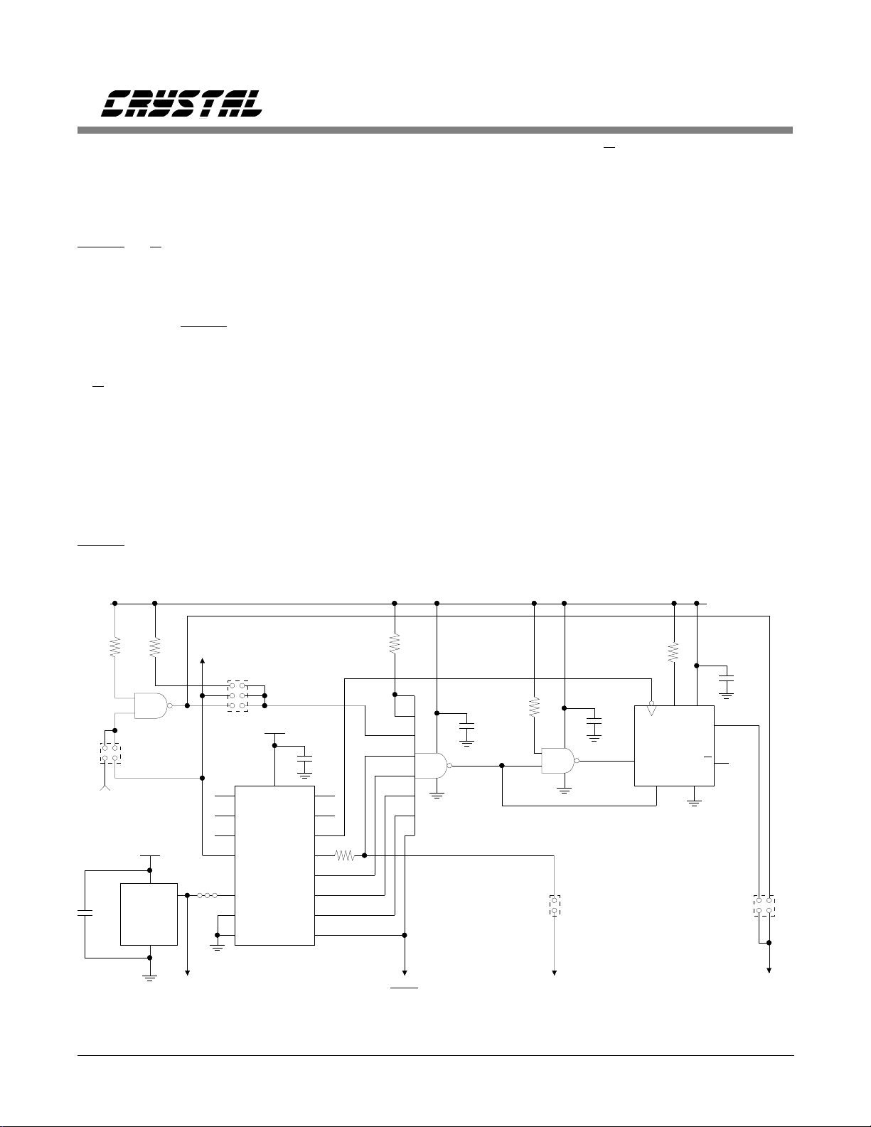
Sampling Clock Generation Logic
The CS5126 requires an external serial clock to
clock out the data. The CDB5126 board has the
logic necessary to generate the master clock,
HOLD, L/R, and SCLK to allow fast evaluation
of the ADC. In most systems, these timing signals will be available from the main timing
section, typically generated by a logic array of
some variety. HOLD may be brought in externally via a
BNC, optionally terminated by R29. SCLK and
L/R select may be brought in externally via test
points and removing jumpers.
Figure 5 shows the on-board clock generation
circuitry. U7 (74HC4040) produces binary divided ratios of the 24.576 MHz master clock. Q4
generates a 1.5 MHz clock, which is used for
SCLK. Q8 generates a 96 kHz clock, used for
HOLD, and Q9 generates a 48 kHz clock, option-
ally used to toggle L/R select. This set of clocks
causes the CS5126 to continuously convert, generating a continuous stream of serial data bits. To
correctly identify the last bit of each word, U12
produces a pulse only when Q4, Q5, Q6, Q7, Q8,
and optionally Q9 are all high. This state is
latched by U10A to prevent any glitches, and the
resulting signal (attached to TP18) is used to
latch the U8-U9 shift registers.
Serial to Parallel Conversion
Figure 6 shows the serial to parallel conversion
circuit. Two 74HC595 shift register/latches connected in series with SDATA assemble 16-bit,
parallel words, clocked by SCLK. As discussed
above, the outputs are latched inside the
74HC595 at the end of each 16-bit word. The
outputs are brough t out to a 40-way header (P 5).
Only low capacitance, twisted pair, ribbon cable
should be used.
+5VL
R16
p.4
47 k
01
U11, pin 8
C28
µ
F
0.1
R18
47 k
12
U11
13
P12
+5VL
14
U6
OUT
Crystal
Oscillator
Module
7
(CLKIN)
11
8
P1
P4
R19
47 k
P10
0
1
2
+5VL
C29
0.1 µF
16
9
Q1
7
Q2
6
Q3
5
Q4
3
Q5
2
Q6
4
74HCT4040
Q7
13
Q8
R28
470
15
14
12
10
11
1
Q12
Q11
U7
Q10
Q9
CLK
RST
8
5
6
3
4
12
2
11
1
P2
(HOLD)
14
U12
7
C32
0.1
8
74HC30
R16, p.3
47 k
µ
F
14
2
U11
1
P3
U8, U9
Shift CLK
7
P9
3
74HC00
C30
0.1
R16, p.5
µ
F
14
47 k
1
2
CLR
U10A
74HC73
J
K
311
C31
0.1 µF
4
12
Q
13
Q
P7
10
U8, U9
Latch CLK
Figure 5. Timing Generator
DS32DB5 25

P9, P3
P7
SDATA (U1)
TRKL (U1)
TRKR (U1)
+5VL
F
µ
0.1
74HC00
10
U11
9
11
12
14
16
C5
12
11
14
+5VL
R 31
47 k
RST
Shift CLK
Latc h C LK
74HC595
8
DATA IN
9
DATA OUT
8
74HC595
Latch CLK
Shift CLK
DATA IN
R 30
47 k
TP 18
P12
TP 17
8
10
U9
U8
OE
13
13
OE
RST
10
R16, p.9
47 k
16
+5VL
P11
Q
H
Q
G
Q
F
Q
E
Q
D
Q
C
Q
B
Q
A
Q
H
Q
G
Q
F
Q
E
Q
D
Q
C
Q
B
Q
A
+5VL
1
0
C3
0.1 µF
7
6
5
4
3
2
1
15
7
6
5
4
3
2
1
15
R16, p.7
47 k
74HC00
10
KRST
7
J
74HC73
5
+5VL
5
U10B
R 22
47 k
U11
R16, p.6
4
6
6
8
Q
47 k
P6
DACK
P8
0
1
2
3
4
CDB5126
CS
D15 (MSB)
D14
D13
D12
D11
D10
D9
D8
40 way
P5
header
D7
D6
D5
D4
D3
D2
D1
D0 (LSB)
DRDY
Figure 6. Seria l to Parall el Converte r
26 DS32DB5

CDB 5126
J1 - Joins analog ground to digital ground on the board.
J2 - Joins LT1019-5 reference directly to the VREF pin on the ADC. Before doing this, break the connection
between R3 and the ADC VREF pin by using a twist drill to remove the central feedthrough. This option
allows evaluation of different reference configurations.
J4 - Connects an external clock to CLKIN on the ADC.
Table 1. Solder Link Options
P1 0 - Select external clock via BNC connector
∗ 1 - Select on-board clock generated by U6.
P2 ∗ 0 - Select on-board generated HOLD.
1 - S elect external HOLD via BNC connector.
P3 ∗ Connect SCLK to on-board shift registers.
P4 ∗ 0 − Pull L/R select pin high, selecting the left channel only.
1 - Drive L/R select at 48 kHz from the on-board timing generator.
2 - Pull L/R select pin low, selecting the right channel only.
P6 ∗ Connect the OE pins of the shift registers to ground. Permanently enables the 3-state output buffers.
P7 ∗ 0 - Connects the on-board Data Ready signal to the shift registers.
1 - Connects the NAND gate outputs (U11, pin 11) to the shift registers.
P8 ∗ 1 - Connects the un-latched on-board Data Ready signal to P5.
2 - Connects TRKL and TRKR
indicator.
3 - Connects TRKL to P5.
4 - Connects TRKR to P5.
P9 ∗ Connects the on-board generated SCLK to the rest of the on-board circuitry.
P10 ∗ 0 - Causes the on-board Data Ready generating circuit to flag data ready every conversion.
1 - Causes the on-board Data Ready generating circuit to flag data ready every left conversion. P4 must
be in position 1 for this to work.
2 - Causes the on-board Data Ready generating circuit to flag data ready every right conversion. P4 must
be in position 1 for this to work.
P11 0 - Connects TRKL & TRKR to U10B, the handshake flip-flop.
ANDED
together to P5. This signal can be used as an "End of Convert"
∗ 1 - Connects the on-board data ready signal to U10B.
P12 ∗ 0 - A llows selection of the DRDY signals for alternate channels.
1 - Connects the TRKL & TRKR to U11, pin 13.
∗
Factory default state for CS5126
Table 2. Shorting Plug Selectable Options
DS32DB5 27

Test Points
CDB5126
U10B (74HC73) is used as a handshake flip-flop
with the computer system attached to the evaluation board. The board brings DRDY low. The
computer reads the data and then sets DACK momentarily high. This resets U10B for the next
word. This handshake can be disabled by setting
P8 jumper to position 1.
DIP Switches
Figure 7 and Table 3 shows the DIP switch selectable options.
SLEEP mode
set at logic "1" for CS51 26
set at logic "1" for CS5126
Output Encoding
No Connect
(user option )
Table 4 is a list of the test points provided on the
Evaluation Board.
CS5126
TP1 VREF
TP2 AINR
TP3 AINL
TP4 AGND
TP5 SSH2
TP6 SSH1
TP7 TRKR
TP8 TRKL
TP9 STBY
TP10 NC
TP11 L/R
TP12 SCLK
TP13 HOLD
TP14 SDATA
TP15 CLKIN
ON
1
Logic "0" = ON = CLOSED / Log ic "1" = OFF = OPEN
Switch Logic Mode
1
2, 3, 4 s et to "1" f or CS51 26
5
6
28 DS32DB5
24
OPEN
Figure 7. DIP switch configuration
0 SLEEP mode
1 Normal mode
0 Offset binary output c ode
1 2’s complement output code
Unconnected. Availa ble for
user’s applications
Table 3. DIP Switch Selection Options
56
TP16 DGND
TP17 TRKL + TRKR
TP18 Latch Clock for the 74HC595
shift registers
Table 4. CDB5126 Test Points

CDB5126
Miscellaneous Hints on Using the Evaluation
Board
Always hit the reset button after powering-up the
board. The CS5126 is self calibrating and require
the reset signal to initiate the calibration procedure.
P4 controls the ADC input mux. This is used to
set the mux to be continuously connected to one
channel, or to be toggling between two channels.
This is very useful for evaluating oversampled
vs. regular sampling digital audio.
P10 controls the Data Ready pulses from the onboard logic. To cause every data sample to be
read, select option 0. If you wish to read only
every alternate sample, then select option 1 or 2,
depending on whether yo u wish to read every left
channel val ue, or every right chan nel value. This
is useful for evaluating the part with a test system
which does not separate alternate values.
CDBCAPTURE Interface
Figure 8 illustrates the CDBCAPTURE interface
that can be constructed in the digital patch area.
A 2-row, 10 pin stake header is wired as show n.
Circuit Board
(Top View)
GND(GND-Digital Patch) +5V
GND
GND
GND
GND
Figure 8. CDBCAPTURE Header Signal Pattern
DS32DB5 29
+5V
FRAME
SCLK
SDATA
(+5VL - Digital Patch)
(+5VL - Digital Patch)
(DRDY - P8)
(SCLK - U9-11)
(SDATA - U8-14)

CDB 5126
Figure 9. CDB 51 26 Co mp one nt L ayo ut
30 DS32DB5

• Notes •
CDB 5126
DS32DB5 31

 Loading...