

Page 1
NTSC/PAL Digital Video Encoder
CS4954
CS4955
Features
l Six DACs provid ing si multan eo us composi te,
S-video, and RGB or Component YUV
outputs
l Programmable DAC ou tput currents for low
imped-ance (37.5 Ω) and high impedance
(150 Ω) loads.
l Multi-standard support for NTSC-M, NTSC-
JAPAN, PAL (B, D, G, H, I, M, N,
Combination N)
l ITU R.BT656 input mode supporting
EAV/SAV codes and CC IR601 Master /Slave
input modes
l Programmable HS YNC and VSYNC timing
l Multistandard Teletext (Europe, NABTS,
WST) support
l VBI encoding support
l Wide-Screen Signaling (WSS) support, EIA-J
CPX1204
l NTSC closed caption encoder with interrupt
l CS4955 supports Macrovision copy
protection Version 7
l Host interface configurable
for parallel or I2C
compatible operation
l On-chip voltage reference
generator
l +3.3 V or +5 V operation,
CMOS, low-power modes,
tri-state DACs
CLK
SCL
SDA
PDAT[7:0]
RD
WR
ADDR
XTAL_IN
XTAL_OUT
TTXDAT
TTXRQ
VD[7:0]
HSYNC
VSYNC
FIELD
INT
RESET
8
8
Description
The CS4954/5 provides full conversion from digital video
formats YCbCr or YUV into NT SC a nd PA L Com posite ,
Y/C (S-video) and RGB, or YUV analog video. Input formats can be 27 MHz 8-bit YUV, 8-bit YCbCr, or ITU
R.BT656 with support for EAV/SAV codes. Video output
can be formatted to be compatible with NTSC-M, NTSCJ, PAL-B,D,G,H,I,M,N, and Combination N systems.
Closed Caption is supported in NTSC. Teletext is supported for NTSC and PAL.
Six 10-bit DACs provide two channels for an S-Video
output port, one or two composite video outputs, and
three RGB or YUV outputs. Two-times oversampling reduces the output filter requi rements and guarante es no
DAC-related modulation components within the specified bandwidth of any of the supported video standards.
Parallel or high-speed I
provided for flexibility in system design. The parallel interface
doubles as a general purpose I/O port when th e CS4954/5 is
2
in I
C mode to help conserve valuable board area.
ORDERING INFORMATION
CS4954-CQ 48-pin TQFP
CS4955-CQ 48-pin TQFP
I2C Interface
Control
Host
Parallel
Interface
Color Sub-carrier Synthesizer
Teletext
Encoder
Video Formatter
Video Timing
Generator
Registers
YCbCr to RBG
Color Space
Converter
DGND
2
VAA
Output
Interpolate
Chroma Amplifier
Chroma Modulate
Chroma Interpolate
U,V
Y
Luma Interpolate
Luma Amplifier
Sync Insert
RGB
C compatible control interfaces are
Burst Ins e rt
LPF
Y
LPF
Y
RGB
Σ
10-Bit
DAC
10-Bit
DAC
10-Bit
DAC
10-Bit
DAC
10-Bit
DAC
10-Bit
DAC
Voltage
Reference
Current
Reference
TEST
C
CVBS
Y
R
G
B
VREF
ISET
Preliminary Product Information
Cirrus Logic, Inc.
P.O. Box 17847, Austin, Texas 78760
(512) 445 7222 FAX: (512) 445 7581
http://www.crystal.com
This document contains information for a new product.
Cirrus Logic reserves the right to modify this product without notice.
Copyright Cirrus Logic, Inc. 1999
(All Rights Reserved)
DS278PP4
APR ‘99
1
Page 2

TABLE OF CONTENTS
1. CHARACTERISTICS AND SPECIFICATIONS ..................................................................5
AC & DC PARAMETRIC SPECIFICATIONS ................................................ ...... ..... ...... .....5
RECOMMENDED OPERATING CONDITIONS .....................................................................5
DC CHARACTERISTICS ....................................................................................................5
AC CHARACTERISTIC .......................................................................................................7
TIMING CHARACTERISTICS .............................................................................................8
2. ADDITIONAL CS4954/5 FEATURES ...............................................................................10
3. CS4954 INTRODUCTION .................................................................................................10
4. FUNCTIONAL DESCRIPTION ................... ....................................... ...... ..... ...... ..... .........10
4.1. Video Timing Generator .........................................................................................10
4.2. Video Input Formatter .............................................................................................11
4.3. Color Subcarrier Synthesizer ..................................................................................11
4.4. Chroma Path ..........................................................................................................11
4.5. Luma Path ..............................................................................................................12
4.6. RGB Path and Component YUV Path ....................................................................12
4.7. Digital to Analog Converters ...................................................................................12
4.8. Voltage Reference ..................................................................................................13
4.9. Current Reference ....................................... ....................................... ...... ..............13
4.10. Host Interface .........................................................................................................13
4.11. Closed Caption Services ........................................................................................13
4.12. Teletext Services ....................................................................................................14
4.13. Wide-Screen Signaling Support and CGMS ...................... ...... ...... ..... ...... ..............14
4.14. VBI Encoding ............................................................................................ ..... .........14
4.15. Control Registers ....................................................................................................14
4.16. Testability ...............................................................................................................14
5. OPERATIONAL DESCRIPTION .......................................................................................14
5.1. Reset Hierarchy ......................................................................................................14
5.2. Video Timing ...........................................................................................................15
5.2.1. Slave Mode Input Interface ..........................................................................15
5.2.2. Master Mode Input Interface ........................................................................15
5.2.3. Vertical Timing ............................................. ...... ..... ...... ...............................16
5.2.4. Horizontal Timing .........................................................................................16
5.2.5. NTSC Interlaced ..........................................................................................16
5.2.6. PAL Interlaced .............................................................................................16
5.2.7. Progressive Scan ......................................................................................... 17
5.2.8. NTSC Progressive Scan ..............................................................................17
5.2.9. PAL Progressive Scan .................................................................................18
5.3. ITU-R.BT656 ..........................................................................................................18
5.4. Digital Video Input Modes .......................................................................................21
5.5. Multi-standard Output Format Modes .....................................................................21
5.6. Subcarrier Generation ............................................................................................21
5.7. Subcarrier Compensation .......................................................................................21
5.8. Closed Caption Insertion ........................................................................................22
5.9. Programmable H-sync and V-sync .........................................................................22
5.10. Wide Screen Signaling (WSS) and CGMS .............................................................23
CS4954 CS4955
Contacting Cirrus Logic Support
For a complete listing of Direct Sales, Distributor, and Sales Representative contacts, visit the Cirrus Logic web site at:
http://www.cirrus.com/corporate/contacts/
Preliminary product info rmation describes products which are i n p r od ucti on, b ut for which full characterizat i on da t a i s not yet available. Advance produ ct i nf or mation describes products which are in development and subject to development changes. Cirrus Logic, Inc. has made best efforts to ensure that the information
contained in this document is accurate and reli able. However , the i nformati on is sub ject to change with out no tice and i s provi ded “AS IS” withou t warranty of
any kind (express or implied). No responsibility is assumed by Cirrus Logic, Inc. for the use of this information, nor for infringements of patents or other rights
of third parties. This document i s the propert y of Cirru s Logic, Inc. and implie s no licen se under patent s, copyri ghts, trademarks, or tr ade secrets. No part of
this publication may be copied, reproduced , stored in a retrieval system, or transmitted, in any form or by any means (electronic, mechanical, photographic, or
otherwise) without the pri or wri tt en consen t of Ci rrus Logic, Inc. Items from any Cirrus Logic websi t e or di sk may be pri nted for use by the user. However, no
part of the printout or electronic files may be copied, reproduced, stored in a retrieval system, or transmitted, in any form or by any means (electronic, mechanical,
photographic, or otherwise) without the prior written consent of Cirrus Logic, Inc.Furthermore, no part of this publication may be used as a basis for manufacture
or sale of any items without the prior written consent of Cirrus Logic, Inc. The names of products of Cirrus Logic, Inc. or other vendors and suppliers appearing
in this document may be trademarks or service marks of their respective owners which may be registered in some jurisdictions. A list of Cirrus Logic, Inc. trademarks and service marks can be found at http://www.cirrus.com.
2 DS278PP4
Page 3

CS4954 CS4955
5.11. Teletext Support .....................................................................................................23
5.12. Color Bar Generator ...............................................................................................25
5.13. VBI encoding .............................. ...... ..... ...... ...... ....................................... ..... .........25
5.14. Super White/Super Black support ........................................... ...... ..... ....................26
5.15. Interrupts ................................................................................................................26
5.16. General Purpose I/O Port .......................................................................................26
6. FILTER RESPONSES ......................................................................................................27
7. ANALOG ..........................................................................................................................30
7.1. Analog Timing ........................................................................................................30
7.2. VREF ...................................................................................................................... 30
7.3. ISET .......................................................................................................................30
7.4. DACs ...................................................................................................................... 30
7.4.1. Luminance DAC ..........................................................................................30
7.4.2. Chrominance DAC ......................................................................................30
7.4.3. CVBS DAC ..................................................................................................31
7.4.4. Red DAC .....................................................................................................31
7.4.5. Green DAC ..................................................................................................31
8. PROGRAMMING .............................................................................................................. 32
9. BOARD DESIGN AND LAYOUT CONSIDERATIONS ....................................................50
10. PIN DESCRIPTION ............................. ...... ....................................... ...... ..... ....................53
11. PACKAGE DRAWING ......................................................................................................55
7.4.6. Blue DAC .....................................................................................................31
8.1. Host Control Interface ............................................................................................32
8.2. Register Description .......................................................... ...... ...............................34
9.1. Power and Ground Planes .....................................................................................50
9.2. Power Supply Decoupling ......................................................................................50
9.3. Digital Interconnect ................................................................................................50
9.4. Analog Interconnect ...............................................................................................50
9.5. Analog Output Protection .......................................................................................51
9.6. ESD Protection .......................................................................................................51
9.7. External DAC Output Filter .....................................................................................51
2
8.1.1. I
8.1.2. 8-bit Parallel Interface .................................................................................33
8.2.1. Control Registers .........................................................................................34
C Interface ................................................................................................32
DS278PP4 3
Page 4

TABLE OF FIGURES
1. Video Pixel Data and Control Port Timing .........................................................................7
2
2. I
C Host Port Timing ..........................................................................................................8
3. Reset Timing ......................................................................................................................9
4. ITU R.BT601 Input Slave Mode Horizontal Timing ..........................................................15
5. ITU R.BT601 Input Master Mode Horizontal Timing ........................................................15
6. Vertical Timing ............ ....... ...... ....... ...... ....... ...... ....... ...... ...... ....................................... ....17
7. NTSC Video Interlaced Timing ........................................................................................18
8. PAL Video Interlaced Timing ...........................................................................................19
9. NTSC Video Non-Interlaced Progressive Scan Timing ...................................................20
10. PAL Video Non-Interlaced Progressive Scan Timing ......................................................20
11. CCIR656 Input Mode Timing ...........................................................................................21
12. Teletext Timing (Pulsation Mode) ....................................................................................24
13. Teletext Timing (Window Mode) ......................................................................................24
14. 1.3 Mhz Chrominance low-pass filter transfer characteristic ...........................................27
15. 1.3 Mhz Chrominance low-pass filter transfer characterstic (passband) .........................27
16. 650 kHz Chrominance low-pass filter transfer characteristic ...........................................27
17. 650 kHz Chrominance low-pass filter transfer characteristic (passband) ........................27
18. Chrominance output interpolation filter transfer characteristic (passband) ......................28
19. Luminance interpolation filter transfer characteristic .......................................................28
20. Luminance interpolation filter transfer characterstic (passband) .....................................28
21. Chrominance interpolation filter transfer characteristic for RGB datapath .......................28
22. Chroma Interpolator for RGB Datapath when rgb_bw=1 (Reduced Bandwidth) .............29
23. Chroma Interpolator for RGB Datapath when rgb_bw=1 (Reduced Bandwidth) .............29
24. Chroma Interpolator for RGB Datapath when rgb_bw=0 -3 dB .......................................29
25. Chroma Interpolator for RGB Datapath when rgb_bw=0 (Full Scale) ..............................29
2
26. I
C Protocol .....................................................................................................................32
27. 8-bit Parallel Host Port Timing: Read-Write/Write-Read Cycle ........................................33
28. 8-bit Parallel Host Port Timing: Address Read Cycle ......................................................33
29. 8-bit Parallel Host Port Timing: Address Write Cycle .......................................................34
30. External Low Pass Filter C
31. Typical Connection Diagram ............................................................................................52
should be chosen so that C1 = C2 + C
2
CS4954 CS4955
......................... 51
cable
4 DS278PP4
Page 5
1. CHARACTERISTICS AND SPECIFICATIONS
ABSOLUTE MAXIMUM RATINGS
CS4954 CS4955
AC & DC PARAMETRIC SPECIFICATIONS
Parameter Symbol Min Max Units
Power Supply VAA/VDD -0.3 6.0 V
Input Current Per Pin (Except Supply Pins) -10 10 mA
Output Current Per Pin (Except Supply Pins) -50 +50 mA
Analog Input Voltage -0.3 VAA + 0.3 V
Digital Input Voltage -0.3 VDD + 0.3 V
Ambient Temperature Power Applied -55 + 125 °C
Storage Temperature -65 + 150 °C
WARNING: Operating beyond these limits can result in permanent damage to the device. Normal operation is not
guaranteed at these extremes.
(AGND,DGND = 0 V, all voltages with respect to 0V
RECOMMENDED OPERATING CONDITIONS (AGND,DGND = 0 V, all voltages with respect to 0 V.)
Parameter Symbol Min Typ Max Units
Power Supplies: Digital Analo g VAA/VDD 3.15
4.75
Operating Ambient Temperature TA 0 + 25 + 70 °C
Note: Operation outside the ranges is not recommended.
3.3
5.0
3.45
5.25
V
)
DC CHARACTERISTICS (T
Parameter Symbol Min Typ Max Units
Digital Inputs
High level Input Voltage
V [7:0], PDAT [7:0], Hsync/Vsync/Field/CLKIN
2
High Level Input Voltage I
Low level Input Voltage All Inputs - -0.3 - 0.8 V
Input Leakage Current - -10 - +10
Digital Outputs
High Level Output Voltage lo = -4 mA VOH 2.4 - VDD V
Low level Output Voltage lo = 4 mA VOL - - 0.4 V
Low Level Output Voltage SDA pin only, lo = 6mA VOL - - 0.4 V
Output Leakage Current High -Z Digital Outputs - -10 - + 10
C
= 25° C; VAA, VDD = 5 V; GNDA, GNDD = 0 V.)
A
VIH 2.2 - VDD+0.3 V
VIH 0.7 VDD - - V
µ
A
µ
A
DS278PP4 5
Page 6
CS4954 CS4955
DC CHARACTERISTICS (Continued)
Parameter Symbol Min Typ Max Units
Analog Outputs
Full Scale Output Current CVBS/Y/C/R/G/B (Notes 1, 2, 3) IO 32.9 34.7 36.5 mA
Full Scale Output Current CVBS/Y/C/R/G/B (Notes 1, 2, 4) IO 8.22 8.68 9.13 mA
LSB Current CVBS/Y/C/R/G/B (Notes 1, 2, 3) IB 32.2 33.9 35.7
LSB Current CVBS/Y/C/R/G/B (Notes 1, 2, 4) IB 8.04 8.48 8.92
DAC-to DAC Matching (Note 1) MAT - 2 - %
Output Compliance (Note 1) VOC 0 - + 1.4 V
Output Impedance (Note 1) ROUT - 15 - k
Output Capacitance (Note 1) COUT - - 30 pF
DAC Output Delay (Note 1) ODEL - 4 12 ns
DAC Rise/Fall Time (Note 1, 5) TRF - 2.5 5 ns
Voltage Reference
Reference Voltage Output VOV 1.170 1.232 1.294 V
Reference Input Current (Note 1) UVC - - 10 uA
Power Supply
Supply Voltage VAA, VDD 3.15
4.75
Digital Supply Current IAA1 - 70 - mA
Analog Supply Low-Z (Note 6) IAA2 - 100 - mA
Analog Supply High-Z (Note 7) IAA3 - 60 - mA
Power Supply Rejection Ratio PSRR 0.02 0.05 %/%
3.3
5.0
3.45
5.25
Static Performance
DAC Resolution (Note 1) - - 10 Bits
Differential Non-Linearity (Note 1) DNL -1 +
Integral Non-Linearity (Note 1) INL - 2 +
0.5 + 1 LSB
1+ 2LSB
Dynamic Performance
Differential Gain (Note 1) DG - 2 5 %
Differential Phase (Note 1) DP - +
Hue Accuracy (Note 1) HA - - 2 °
Signal to Noise Ratio SNR 70 - - dB
Saturation Accuracy (Note 1) SAT - 1 2 %
0. 5 + 2 °
µ
µ
V
A
A
Ω
Notes: 1. Values are by characterization only
2. Output current levels with ISET = 4 KΩ , VREF = 1.232 V.
3. DACs are set to low impedance mode
4. DACs are set to high impedance mode
5. Times for black-to-white-level and white-to-black-level transitions.
6. Low-Z - 3 dacs on
7. High-Z - 6 dacs on
6 DS278PP4
Page 7
CS4954 CS4955
AC CHARACTERISTIC
Parameter Symbol Min Typ Max Units
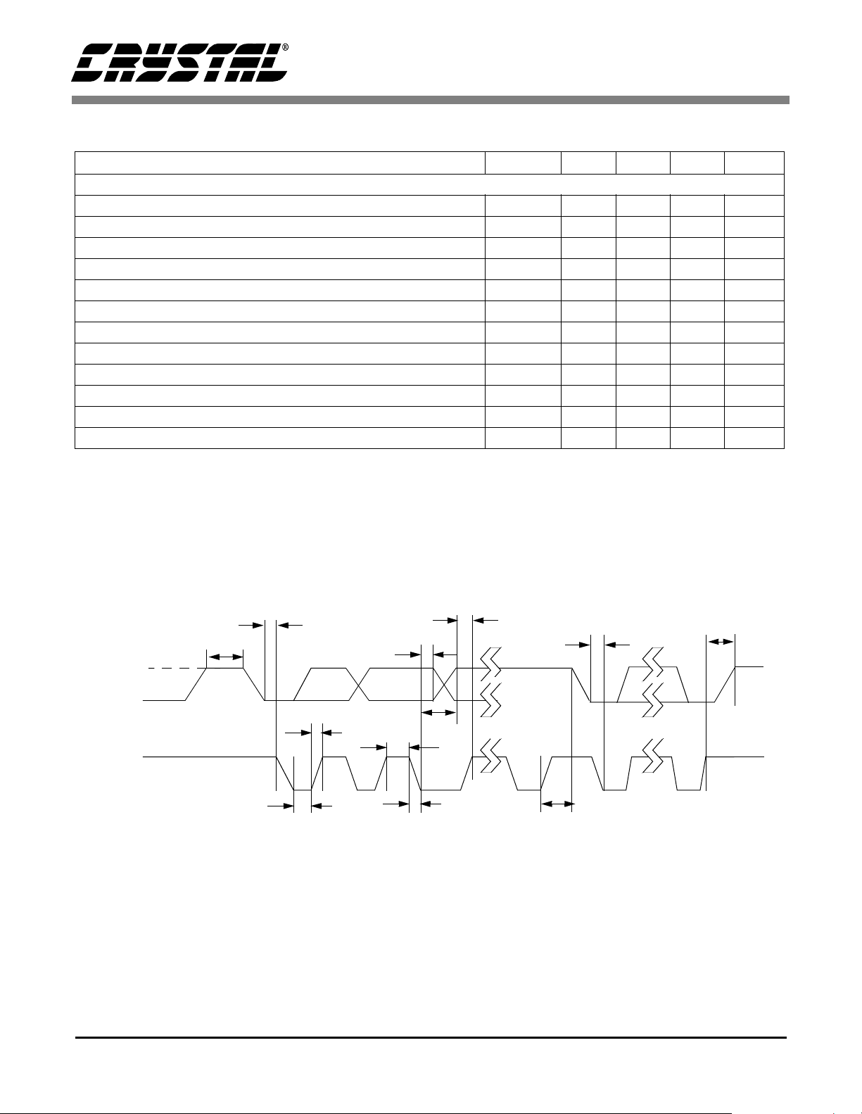
Pixel Input and Control Port (Figure 1)
Clock Pulse High Time Tch 14.82 18.52 22.58 ns
Clock Pulse Low Time Tcl 14.82 18.52 22.58 ns
Clock to Data Set-up Time Tisu 6 - - ns
Clock to Data Hold Time Tih 0 - - ns
Clock to Data Output Delay Toa - - 17 ns
CLK
T
isu
T
chTcl
V[7:0]
HSYNC
HSYNC
/VSYNC
(Inputs)
/VSYNC
CB/FIELD/INT
(Outputs)
T
ih
T
oa
Figure 1. Video Pixel Data and Control Port Timing
DS278PP4 7
Page 8
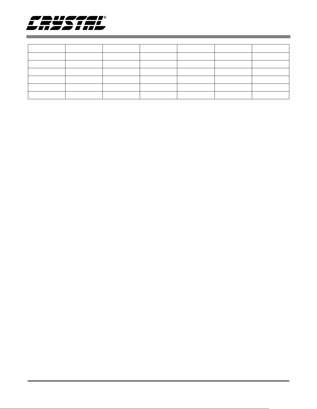
CS4954 CS4955
TIMING CHARACTERISTICS
Parameter Symbol Min Typ Max Units
I2C Host Port Timing (Figure 2)
SCL Frequency Fclk 100 1000 KHz
Clock Pulse High Time Tsph 0.1
Clock Pulse Low Time Tspl 0.7
Hold Time (Start Cond.) Tsh 100 ns
Setup Time (Start Cond.) Tssu 100 ns
Data Setup Time Tsds 50
Rise Time Tsr 1
Fall Time Tsf 0.3
Setup Time (Stop Cond.) Tss 100 ns
Bus Free Time Tbuf 100 ns
Data H old Time Tdh 0 ns
SCL Low to Data Out Valid Tvdo 600 ns
µ
µ
n
µ
µ
s
s
s
s
s
SDA
SCL
T
dh
vdo
ds
T
sh
T
ssu
T
ss
T
sh
T
sph T
T
T
si
T
bu
T
sr
T
spi
Figure 2. I2C Host Port Timing
8 DS278PP4
Page 9

CS4954 CS4955
TIMING CHARACTERISTICS(Continued)
Parallel Host Port Timing (Figure 27, 28, 29)
Read Cycle Time Trd 60 - - ns
Read Pulse Width Trpw 30 - - ns
Address Setup Time Tas 3 - - ns
Read Address Hold Time Trah 10 - - ns
Read Data Access Time Trda - - 40 ns
Read Data Hold Time Trdh 10 - 50 ns
Write Recovery Time Twr 60 - - ns
Write Pulse Width Twpw 40 - - ns
Write Data Setup Time Twds 8 - - ns
Write Data Hold Time Twdh 3 - - ns
Write-Read/Read-Write Recovery Time Trec 50 - - ns
Address from Write Hold Time Twac 0 - - ns
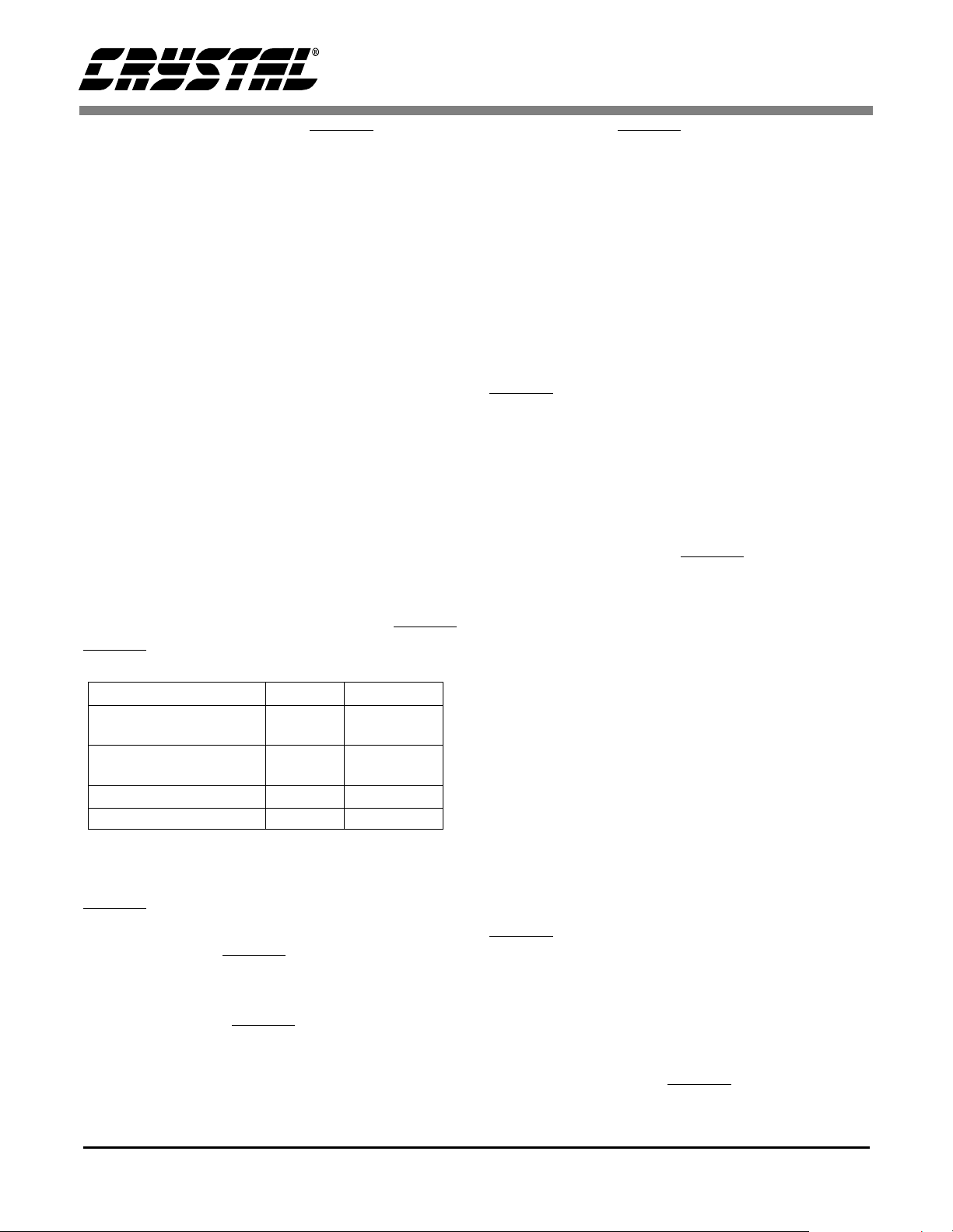
Reset Timing (Figure 3)
Reset Pulse Width Tres 100 ns
RESET*
T
res
Figure 3. Reset Timing
DS278PP4 9
Page 10

CS4954 CS4955
2. ADDITIONAL CS4954/5 FEATURES
• Five programmable DAC output combinations,
including YUV and second composite
• Optional progressive scan @ MPEG2 field rates
• Stable color subcarrier for MPEG2 systems
• General purpose input and output pins
• Individual DAC power-down capability
• On-chip color bar generator
• Supports RS170A and ITU R.BT601 composite output timing
• HSYNC and VSYNC output in ITU R.BT656
mode
• Teletext encoding selectable on two composite
and S-video signals
• Programmable saturation, SCH Phase, hue,
brightness and contrast
• Device power-down capability
• Super White and Super Black support
3. CS4954 INTRODUCTION
The CS4954/5 is a complete multi-standard digital
video encoder implemented in current CMOS technology. The device can operate at 5 V as well as at
3.3 V. ITU R.BT601- or ITU R.BT656-compliant
digital video input is converted into NTSC-M,
NTSC-J, PAL-B, PAL-D, PAL-G, PAL-H, PAL-I,
PAL-M, PAL-N, or PAL-N Argentina-compatible
analog video. The CS4954/5 is designed to connect, without glue logic, to MPEG1 and MPEG2
digital video decoders.
Two 10-bit DAC outputs provide high quality SVideo analog output while another 10-bit DAC simultaneously generates composite analog video. In
addition, there are three more DACs to provide simultaneous analog RGB or analog YUV outputs.
The CS4954/5 will accept 8-bit YCbCr or 8-bit
YUV input data.
The CS4954/5 is completely configured and controlled via an 8-bit host interface port or an I2C
compatible serial interface. This host port provide s
access and control of all CS4954/5 options and features, such as closed caption insertion, interrupts,
etc.
In order to lower overall system costs, the
CS4954/5 provides an internal voltage reference
that eliminates the requirement for a n external, discrete, three-pin voltage reference.
In ISO MPEG-2 system configurations, the
CS4954/5 can be augmented with a common colorburst crystal to provide a stable color subcarrier
given an unstable 27 MHz clock input. The use of
the crystal is optional, but the facility to connect
one is provided for MPEG-2 environments in
which the system clock frequency variability is too
wide for accurate color sub-carrier generation.
4. FUNCTIONAL DESCRIPTION
In the following subsections, the functions of the
CS4954/5 will be described. The descriptions refer
to the device elements shown in the block diagram
on the cover page.
4.1. Video Timing Generator
All timing generation is accomplished via a
27 MHz input applied to the CLK pin. The
CS4954/5 can also accept a signal from an optional
color burst crystal on the XTAL_IN &
XTAL_OUT pins. See the section, Color Subcarrier Synthesizer, for further details.
The Video Timing Generator is responsible for orchestrating most of the other modules in the device.
It operates in harmony with external sync input
timing, or it can provide external sync timing outputs. It automatically disables color burst on appropriate scan lines and automatically generates
serration and equalization pulses on appropriate
scan lines.
10 DS278PP4
Page 11

CS4954 CS4955
The CS4954/5 is designed to function as a video
timing master or video timi ng slave. In both Master
and Slave Modes, all timing is sampled and asserted with the rising edge of the CLK pin.
In most cases, the CS4954/5 will serve as the video
timing master. HSYNC, VSYNC, and FIELD are
configured as outputs in Master Mode. HSYNC or
FIELD can also be defined as a composite blanking
output signal in Master Mode. In Master Mode, the
timing of HSYNC, VSYNC, FIELD and Composite Blank (CB) signals is programmable. Exact horizontal and vertical display timing is addressed in
the Operational Description section.
In Slave Mode, HSYNC and VSYNC are typically
configured as input pins and are used to initialize
independent vertical and horizontal timing generators upon their respective falling edges. HSYNC
and VSYNC timing must conform to the ITUR BT.601 specifications.
CLK input (27 MHz). Color burst accuracy and
stability are limited by the accuracy of the 27 MHz
input. If the frequency varies, then the color burst
frequency will also vary accordingly.
For environments in which the CLK input varies or
jitters unacceptably, a local crystal frequency reference can be used on the XTAL_IN and
XTAL_OUT pins. In this instance, the input CLK is
continuously compared with the external crystal reference input and the internal timing of the CS4954/5
is automatically adjusted so that the color burst frequency remains within tolerance.
Controls are provided for phase adjustment of the
burst to permit color adjustment and phase compensation. Chroma hue control is provided by the
CS4954/5 via a 10-bit Hue Control Register
(HUE_LSB and H_MSB). Burst amplitude control
is also made available to the host via the 8-bit burst
amplitude register (SC_AMP).
The CS4954/5 also provides a ITU R.BT656 Slave
Mode in which the video input stream contains
EAV and SAV codes. In this case, proper HSYNC
and VSYNC timing are extracted automatically
without any inputs other than the V [7:0]. ITU
R.BT656 input data is sampled with the leading
edge of CLK.
In addition, it is also possible to output HSYNC
and VSYNC signals during CCIR-656 Slave
Mode.
4.2. Video Input Formatter
The Video Input Formatter translates YCbCr input
data into YUV information, when necessary, and
splits the luma and chroma information for filtering, scaling, and modulation.
4.3. Color Subcarrier Synthesizer
The subcarrier synthesizer is a digital frequency
synthesizer that produces the appropriate subcarrier frequency for NTSC or PAL. The CS4954/5
generates the color burst frequency based on the
4.4. Chroma Path
The Video Input Formatter delivers 4:2:2 YUV
outputs into separate chroma and luma data paths.
The chroma path will be discussed here.
The chroma output of the Video Input Formatter is
directed to a chroma low-pass 19-tap FIR filter.
The filter bandwidth is selected (or the filter can be
bypassed) via the CONTROL_1 Register. The
passband of the filter is either 650 KHz or 1.3 MHz
and the passband ripple is less than or equal to
0.05 dB. The stopband for the 1.3 MHz selection
begins at 3 MHz with an attenuation of greater than
35 dB. The stopband for the 650 KHz selection begins around 1.1 MHz with an attenuation of greater
than 20 dB.
The output of the chroma low-pass filter is connected to the chroma interpolation filter in which upsampling from 4:2:2 to 4:4:4 is accomplished.
Following the interpolation filter, the U and V
chroma signals pass through two independent variable gain amplifiers in which the chroma amplitude
DS278PP4 11
Page 12

CS4954 CS4955
can be varied via the U_AMP and V_AMP 8-bit
host addressable registers.
The U and V chroma signals are fed to a quadrature
modulator in which they are combined with the
output from the subcarrier synthesizer to produce
the proper modulated chrominance signal.
The chroma then is interpolated by a factor of two
in order to operate the output DACs at twice the
pixel rate. The interpolated filters enable running
the DACs at twice the pixel rate and this helps reduce the sinx/x roll-off for higher frequencies and
reduces the complexity of the external analog low
pass filters.
4.5. Luma Path
Along with the chroma output path, the CS4954/5
Video Input Formatter initiates a parallel luma data
path by directing the luma data to a digital delay
line. The delay line is built as a digital FIFO in
which the depth of the FIFO replicates the clock
period delay associated with the more complex
chroma path. Brightness adjustment is also provided via the 8-bit BRIGHTNESS_OFFSET Register.
Following the luma delay, the data is passed
through an interpolation filter that has a programmable bandwidth, followed by a variable gain amplifier in which the luma DC values are mod ifi abl e
via the Y_AMP Register.
three pixel clocks. This variable delay is useful to
offset different propagation delays of the luma
baseband and modulated chroma signals. This adjustable luma delay is available only on the
CVBS_1 output.
4.6. RGB Path and Component YUV Path
The RGB datapath has the same latency as the luma
and chroma path. Therefore all six simultaneous
analog outputs are synchronized. The 4:2:2 YCbCr
data is first interpolated to 4:4:4 and then interpolated to 27 MHz. The color space conversion is performed at 27 MHz. The coefficients for the color
space conversion conform to the ITU R.BT601
specifications.
After color space conversion, the amplitude of each
component can be independently adjusted via the
R_AMP, G_AMP, and B_AMP 8-bit host addressable registers. A synchronization signal can be added to either one, two or all of the RGB signals. The
synchronization signal conforms to NTSC or PAL
specifications.
Some applications (e.g., projection TVs) require
analog component YUV signals. The chip provides
a programmable mode that outputs component
YUV data. Sync can be added to the luminance signal. Independent gain adjustment of the three components is provided as well.
The output of the luma amplifier connects to the
sync insertion block. Sync insertion is accomplished by multiplexing, into the luma data path,
the different sync DC values at the appropriate
times. The digital sync generator takes horizontal
sync and vertical sync timing signals and generates
the appropriate composite sync timing (including
vertical equalization and serration pulses), blanking information, and burst flag. The sync edge rates
conform to RS-170A or ITU R.BT601 and ITU
R.BT470 specifications.
It is also possible to delay the luminance signal,
with respect to the chrominance signal, by up to
12 DS278PP4
4.7. Digital to Analog Converters
The CS4954/5 provides six discrete 27 MHz DACs
for analog video. The default configuration is one
10-bit DAC for S-video chrominance, one 10-bit
DAC for S-Video luminance, one 10-bit DAC for
composite output, and three 10-bit DACs for RGB
outputs. All six DACs are designed for driving either low-impedance loads (double terminated
75 Ω) or high-impedance loads (double terminated
300 Ω). There are five different DAC configurations to choose from (see Table 1, below).
The DACs can be put into tri-state mode via hostaddressable control register bits. Each of the six
Page 13
CS4954 CS4955
DAC Pin # Mode 1 Mode 2 Mode 3 Mode 4 Mode 5
Y 48 Y Y Y CVBS_2 CVBS_2
C47CCC- -
CVBS 44 CVBS_1 CVBS_1 CVBS_1 CVBS_1 CVBS_1
R 39 R Cr (V) - R Cr (V)
G 40 G Y CVBS_2 G Y
B43BCb (U)- BCb (U)
Table 1. DAC configuration Modes
DACs has its own associated DAC enable bit. In
the Disable Mode, the 10-bit DACs source (or sink)
zero current.
When running the DACs with a low-impedance
load, a minimum of three DACs must be powered
down. When running the DACs with a high-impedance load, all the DACs can be enabled simultaneously.
For lower power standby scenarios, the CS4954/5
also provides power shut-off control for the DACs.
Each DAC has an associated DAC shut-off bit.
4.8. Voltage Reference
The CS4954/5 is equipped with an on-board voltage reference generator (1.232 V) that is used by
the DACs. The internal reference voltage is accurate enough to guarantee a maximum of 3% overall
gain error on the analog outputs. However, it is
possible to override the internal reference voltage
by applying an external voltage source to the VREF
pin.
output current modes are software selectable
through a register bit.
4.10. Host Interface
The CS4954/5 provides a parallel 8-bit data interface for overall configuration and control. The host
interface uses active-low read and write strobes,
along with an active-low address enable signal, to
provide microprocessor-compatible read and write
cycles. Indirect host addressing to the CS4954/5 internal registers is accomplished via an internal a ddress register that is uniquely accessible via bus
write cycles in which the host address enable signal
is asserted.
The CS4954/5 also provides an I2C-compatible serial interface for device configuration and control.
This port can operate in standard (100Kb/sec) or
fast (400 Kb/sec) modes. When in I2C mode, the
parallel data interface pins, PDAT [7:0], can be
used as a general purpose I/O port controlled by the
I2C interface.
4.9. Current Reference
The DAC output current-per-bit is derived in the
current reference block. T he current step is specified by the size of resistor placed between the ISET
current reference pin and electrical ground.
4.11. Closed Caption Services
The CS4954/5 supports the generation of NTSC
Closed Caption services. Line 21 and Line 284 captioning can be generated and enabled independently via a set of control registers. When enabled,
clock run-in, start bit, and data bytes are automati-
A 4 kΩ resistor needs to be connected between
ISET pin and GNDA. The DAC output currents are
optimized to either drive a doubly terminated load
of 75 Ω (low impedence mode) or a double termi-
cally inserted at the appropriate video lines. A convenient interrupt protocol simplifies the software
interface between the host processor and the
CS4954/5.
nated load of 300 Ω (high impedence mode). The 2
DS278PP4 13
Page 14

CS4954 CS4955
4.12. Teletext Services
The CS4954/5 encodes the most common teletext
formats, such as European Teletext, World Standard Teletext (PAL and NTSC), and North American Teletext (NABTS).
Teletext data can be inserted in any of the TV lines
(blanking lines as well as active lines). In addition
the blanking lines can be individually allocated for
Teletext instantiation.
The input timing for teletext data is user programmable. See the section Teletext Services for further
details.
Teletext data can be independently inserted on either one or all of the CVBS_1, CVBS_2, or S-video
signals.
4.13. Wide-Screen Signaling Support and
CGMS
Insertion of wide-screen signal encoding for PAL
and NTSC standards is supported and CGMS
(Copy Generation Management System) for NTSC
in Japan. Wide-screen signals are inserted in lines
23 and 336 for PAL, and lines 20 and 283 for
NTSC.
4.14. VBI Encoding
This chip supports the transmission of control signals in the vertical blanking t ime interval according
to SMPTE RP 188 recommendations. VBI encoded
data can be independently inserted into either or all
of CVBS_1, CVBS_2 or S-video signals.
4.15. Control Registers
The control and configuration of the CS4954/5 is
accomplished primarily through the control register block. All of the control registers are uniquely
addressable via the internal address register. The
control register bits are initialized during device
RESET.
See the Programming section of this data sheet for
the individual register bit allocations, bit operational descriptions, and initialization states.
4.16. Testability
The digital circuits are completely scanned by an
internal scan chain, thus providing close to 100%
fault coverage.
5. OPERATIONAL DESCRIPTION
5.1. Reset Hierarchy
The CS4954/5 is equipped with an active low asynchronous reset input pin, RESET. RESET is used to
initialize the internal registe rs and the internal st ate
machines for subsequent default operation. See the
electrical and timing specification section of this
data sheet for specific CS4954/5 device RESET
and power-on signal timing requirements and restrictions.
While the RESET pin is held low, the host interface
in the CS4954/5 is disabled and will not respond to
host-initiated bus cycles. All outputs are valid after
a time period following RESET pin low.
A device RESET initializes the CS4954/5 internal
registers to their default values as described by Table 9, Control Registers. In the default state, the
CS4954/5 video DACs are disabled and the device
is internally configured to provide blue field video
data to the DACs (any input data present on the
V [7:0] pins is ignored at this time). Otherwise, the
CS4954/5 registers are configured for NTSC-M
ITU R.BT601 output operation. At a minimum, the
DAC Registers (0x04 and 0x05) must be written (to
enable the DACs) and the IN_MODE bit of the
CONTROL_0 Register (0x01) must be set (to enable ITU R.BT601 data input on V [7:0]) for the
CS4954/5 to become operational after RESET.
14 DS278PP4
Page 15

NTSC 27MHz Clock Count
PAL 27MHz Clock Count
CLK
HSYNC (input)
V[7:0]
(SYNC_DLY=0)
1682
1702
Y
• • •
CS4954 CS4955
168616851684
1683
1703
Cr
active pixel
#720
17051704
Y Cb Y Cr Y
1706
• • •
• • •
1716
1728
1
23 128
1
23 128
horizontal blanking
• • •
• • •
129
129
• • •
• • •
244 245
264 265
active pixel#1active pixel
246 247
266 267
248
268
#2
V[7:0]
(SYNC_DLY=1)
Y
Cb
active pixel
#719
Cr
Y
active pixel
#720
Figure 4. ITU R.BT601 Input Slave Mode Horizontal Tim ing
5.2. Video Timing
5.2.1. Slave Mode Input Interface
In Slave Mode, the CS4954/5 receives signals on
VSYNC and HSYNC as inputs. Slave Mode is the
default following RESET and is changed to Master
Mode via a control register bit (CONTROL_0 [4]).
The CS4954/5 is limited to ITU R.BT601 horizontal and vertical input timing. All clocking in the
CS4954/5 is generated from the CLK pin. In Slave
Mode, the Sync Generator uses externally provided
horizontal and vertical sync signals to synchronize
the internal timing of the CS4954/5. Video data that
is sent to the CS4954/5 must be synchronized to the
horizontal and vertical sync signals. Figure 4 illustrates horizontal timing for ITU R.BT601 input in
Slave Mode. Note that the CS4954/5 expects to receive the first active pixel data on clock cycle 245
(NTSC) when CONTROL_2 Register (0x02) bit
Cb
Y
Cr
horizontal blanking active pixel#1active pixel
#2
SYNC_DLY = 0. When SYNC_DLY = 1, it expects
the first active pixel data on clock cycle 246 (NTSC).
5.2.2. Master Mode Input Interface
The CS4954/5 defaults to Slave Mode following
RESET high but can be switched into Master Mode
via the MSTR bit in the CONTROL_0 Register
(0x00). In Master Mode, the CS4954/5 uses the
VSYNC, HSYNC and FIELD device pins as outputs to schedule the proper external delivery of digital video into the V [7:0] pins. Figure 5 illustrates
horizontal timing for the CCIR601 input in Master
Mode.
The timing of the HSYNC output is selectable in
the PROG_HS Registers (0x0D, 0x0E). HSYNC
can be delayed by one full line cycle. The timing of
the VSYNC output is also selectable in the
NTSC 27MHz Clock Count
PAL 27MHz Clock Count
CLK
HSYNC (output)
CB (output)
V[7:0]
1682
1702
Y
• • •
1683
1703
Cr
active pixel
#720
17051704
Y Cb Y Cr Y
1706
• • •
• • •
1716
1728
1
23 128
1
23 128
horizontal blanking
• • •
• • •
129
129
• • •
• • •
244 245
264 265
246 247
266 267
active pixel#1active pixel
248
268
#2
168616851684
Figure 5. ITU R.BT601 Input Master Mode Horizontal Timing
DS278PP4 15
Page 16
CS4954 CS4955
Mode Field Active Lines
NTSC 1, 3;
2, 4
22-261;
285-524
P AL 1, 3, 5, 7;
2, 4, 6, 8
23-310;
336-623
NTSC Progressive-Scan NA 22-261
PAL Progressive-Scan NA 23-310
Table 2. Vertical Timing
PROG_VS Register (0x0D). VSYNC can be delayed by thirteen lines or advanced by eighteen lines.
5.2.3. Vertical Timing
The CS4954/5 can be configured to operate in any
of four different timing modes: PAL, which is 625
vertical lines, 25 frames per second interlaced;
NTSC, which is 525 vertical lines, 30 frames per
second interlaced; and either PAL or NTSC in Progressive Scan, in which the display is non-interlaced. These modes are selected in the
CONTROL_0 Register (0x00).
The CS4954/5 conforms to standard digital decompression dimensions and does not process digital
input data for the active analog video half lines as
they are typically in the over/underscan region of
televisions. 240 active lines total per field are processed for NTSC, and 288 active lines total per
field are processed for PAL. Frame vertical dimensions are 480 lines for NTSC and 576 lines for
PAL. Table 2 specifies active line numbers for both
NTSC and PAL. Refer to Figure 6 for HSYNC,
VSYNC and FIELD signal timing.
(falling) edge of HSYNC if the PROG_HS Registers are set to default values.
5.2.5. NTSC Interlaced
The CS4954/5 supports NTSC-M, NTSC-J and
PAL-M modes where there are 525 total lines per
frame and two fixed 262.5-line fields per frame and
30 total frames occurring per second. NTSC inter laced vertical timing is illustrate d in Figure 7. Each
field consists of one line for closed caption, 240 active lines of video, plus 21.5 lines of blanking.
VSYNC field one transitions low at the beginning
of line four and will remain low for three lines or
2574 pixel cycles (858 × 3). The CS4954/5 exclusively reserves line 21 of field one for closed caption insertion. Digital video input is expected to be
delivered to the CS4954/5 V [7:0] pins for 240
lines beginning on active video lines 22 and continuing through line 261. VSYNC field two transitions low in the middle of line 266 and stays low for
three line-times and transitions high in the middle
of line 269. The CS4954/5 exclusively reserves line
284 of field two for closed caption insertion. Video
input on the V [7:0] pins is expected between lines
285 through line 525.
5.2.4. Horizontal Timing
HSYNC is used to synchronize the horizontal-input-to-output timing in order to provide proper horizontal alignment. HSYNC defaults to an input pin
following RESET but switches to an output in Master Mode (CONTROL_0 [4] = 1). Horizontal timing is referenced to HSYNC transitioning low. For
active video lines, digital video input is to be applied to the V [7:0] inputs for 244 (NTSC) or for
264 (PAL) CLK periods following the leading
16 DS278PP4
5.2.6. PAL Interlaced
The CS4954/5 supports PAL modes B, D, G, H, I,
N, and Combination N, in which there are 625 total
lines per frame, two fixed 312.5 line fields per
frame, and 25 total frames per second. Figure 8 illustrates PAL interlaced vertical timing. Each field
consists of 287 active lines of video plus 25.5 lines
of blanking.
VSYNC will transition low to begin field one and
will remain low for 2.5 lines or 2160 pixel cycles
(864 × 2.5). Digital video input is expected to be
delivered to the CS4954/5 V [7:0] pins for 287
lines beginning on active video line 24 and continuing through line 310.
Field two begins with VSYNC transitioning low
after 312.5 lines from the beginning of field one.
Page 17
NTSC Vertical Timing (odd field)
CS4954 CS4955
Line
HSYNC
VSYNC
FIELD
Line
HSYNC
VSYNC
FIELD
Line
HSYNC
VSYNC
FIELD
3
NTSC Vertical Timing (even fiel d)
264 265
PAL Vertical Timing (odd field)
265 1 2
4
5 6
266 267 268 269 270
7 8 9
3 4 5 6
10
271
7
PAL Vertical Timing (even field)
Line
HSYNC
VSYNC
FIELD
311 312
313 314 315 316 317
Figure 6. Vertical Timing
VSYNC stays low for 2.5 line-times and transitions
high with the beginning of line 315. Video input on
the V [7:0] pins is expected between line 336
through line 622.
5.2.7. Progressive Scan
The CS4954/5 supports a progessive scan mode in
which the video output is non-interlaced. This is
accomplished by displaying only the odd video
field for NTSC or PAL. To preserve precise
MPEG-2 frame rates of 30 and 25 per second, the
CS4954/5 displays the same odd field repetitively
but alternately varies the field times. This mode is
in contrast to other digital video encoders, which
318
commonly support progressive scan by repetitively
displaying a 262 line field (524/525 lines for
NTSC). The common method is flawed: over time,
the output display rate will overrun a system-clo cklocked MPEG-2 decompressor and display a field
twice every 8.75 seconds.
5.2.8. NTSC Progressive Scan
VSYNC will transition low at line four to begin
field one and will remain low for three lines or
2574 pixel cycles (858 × 3). NTSC interlaced timing is illustrated in Figure 9. In this mode, the
CS4954/5 expects digital video input at the V [7:0]
DS278PP4 17
Page 18

CS4954 CS4955
Analog
Field 1
523 524 525 1 2 3 4 5 6 7 8 9
Analog
Field 2
261 262 263
Analog
Field 3
523 524 525
261 262 263
Burst begins with positive half-cycle Burst begins with negative half-cycle
1 23456 789
Analog
Field 4
Figure 7. NTSC Video Interlaced Timing
VSYNC Drops
VSYNC Drops
10 22
285284272271270269268267266265264
10 22
285284272271270269268267266265264
pins for 240 lines beginning on active video line 22
and continuing through line 261.
Field two begins with VSYNC transitioning low at
line 266. VSYNC stays low for 3 line cycles and
transitions high during the end of line 268. Video
input on the V [7:0] pins is expected between line
284 and line 522. Field two is 263 lines; field one
is 262 lines.
5.2.9. PAL Progressive Scan
VSYNC will transition low at the beginning of the
odd field and will remain low for 2.5 lines or 2160
pixel cycles (864 × 2.5). PAL non-interlaced timing is illustrated in Figure 10. In this mode, the
CS4954/5 expects digital video input on the V [7:0]
pins for 288 lines, beginning on active video line 23
and continuing through line 309.
The second begins with VSYNC transitioning low
after 312 lines from the beginning of the first field.
VSYNC stays low for 2.5 line-times and transitions
high during the middle of line 315. Video input on
the V [7:0] pins is expected between line 335
through line 622. Field two is 313 lines; field one is
312 lines.
5.3. ITU-R.BT656
The CS4954/5 supports an additional ITUR.BT656 slave mode feature that is selectable
through the ITU-R.BT656 bit of the CONTROL_0
Register. The ITU-R.BT656 slave feature is unique
because the horizontal and vertical timing and digital video are combined into a single 8-bit 27 MHz
input. With ITU-R.BT656 there are no horizontal
and vertical input or output strobes, only 8-bit
27 MHz active CbYCrY data, with start- and endof-video codes implemented using reserved 00 and
FF code sequences within the video feed. As with
all modes, V [7:0] are sampled with the rising edge
of CLK. The CS4954/5 expects the digital ITUR.BT656 stream to be error-free. The F IELD out-
18 DS278PP4
Page 19

CS4954 CS4955
VSYNC Drops
Analog
Field 1
621 622 623
620 624 625 1 2 3 4 5 6 7 23 24
Analog
Field 2
309 310
308 311 312 313 314 315 316 317 318 319 320 336 337
Analog
Field 3
620 624 625 1 2 3 4 5 6 7 23 24
621 622 623
Analog
Field 4
309 310
308 311 312 313 314 315 316 317 318 319 320 336 337
Analog
Field 5
620 624 625 1 2 3 4 5 6 7 23 24
621 622 623
Analog
Field 6
309 310
308 311 312 313 314 315 316 317 318 319 320 336 337
Analog
Field 7
620 624 625 1 2 3 4 5 6 7 23 24
621 622 623
Analog
Field 8
309 310
308 311 312 313 314 315 316 317 318 319 320 336 337
Burst Phase = 135 degrees relative to U Burst Phase = 225 degrees relative to U
Figure 8. PAL Video Interlaced Timing
put toggles as with non ITU-R.BT656 input. ITUR.BT656 input timing is illustrated in Figure 11.
As mentioned above, there are no horizontal and
vertical timing signals necessary in ITU-R.BT656
mode. However in some cases it is advantageous to
output these timing signals for other purposes. By
setting the 656_SYNC_OUT register bit in
CONTROL_6 register, HSYNC and VSYNC are
output,so that other devices in the system can synchronize to these timing signals.
DS278PP4 19
Page 20

CS4954 CS4955
Start of
VSYNC
262 263
261 262
262 263
261 262
Burst begins with positive half-cycle Burst begins with negative half-cycle
Burst phase = refere nce phase = 180 relativ e to B-Y
12345678910 22
12345678910 22
Start of
VSYNC
12345678910 22
123456789
0
Field 1
Field 2
Field 3
Field 4
10 22
Burst phase = refer enc e phase = 180 relative to B-Y
Figure 9. NTSC Video Non-Interlaced Progressive Scan Timing
0
309 310 311
309
308 311 312
309 310 311
309
308 311 312 12345 67 23 24310
Burst Phase = 135 degrees relative to U Burst Phase = 225 degrees relative to U
312 313 1 2 3 4 5 6 7 23 24
312 313 1 2 3 4 5 6 7 23 24
VSYNC Drops
Analog
Field 1
Analog
Field 2
12345 67 23 24310
Analog
Field 3
Analog
Field 4
Figure 10. PAL Video Non-Interlaced Progressive Scan Timing
20 DS278PP4
Page 21

Composite
Video
CS4954 CS4955
ITU R.BT656
DATA
V[7:0]
Y Cr Y FF 00 00 XY 80 10 80 10 80 10 80 10 80 10 80 10 80 10 FF 00 00 XY Cb Y Cr Cb Y Cr
EAV Code
4 Clocks
Active Video
Figure 11. CCIR656 Input Mode Timing
268 Clocks (NTSC)
280 Clocks (PAL)
Horizontal Blanking
5.4. Digital Video Input Modes
The CS4954/5 provides two different digital video
input modes that are selectable through the
IN_MODE bit in the CONTROL_0 Register.
In Mode 0 and upon RESET, the CS4954/5 defaults to output a solid color (one of a possible of
256 colors). The background color is selected by
writing the BKG_COLOR Register (0x08). The
colorspace of the register is RGB 3:3:2 and is unaffected by gamma correction. The default color following RESET is blue.
In Mode 1 the CS4954/5 supports a single 8-bit
27 MHz CbYCrY source as input on the V [7:0]
pins. Input video timing can be ITU-R.BT601 master or slave and ITU-R.BT656.
Ancilliary Data
SAV Code
4 Clocks
1440 Clocks
Active Video
Output formats are configured by writing control
registers with the values shown in Table 3.
5.6. Subcarrier Generation
The CS4954/5 automatically synthesizes NTSC
and PAL color subcarrier clocks using the CLK frequency and four control registers
(SC_SYNTH0/1/2/3). The NTSC subcarrier synthesizer is reset every four fields (every eight fields
for PAL).
The SC_SYNTH0/1/2/3 registers used together
provide a 32-bit value that defaults to NTSC
(43E0F83Eh) following RESET. Table 4 shows the
32-bit value required for each of the different
broadcast formats.
5.5. Multi-standard Output Format Modes
The CS4954/5 supports a wide range of output formats compatible with worldwide broadcast stan-
System Fsubcarrier Value (hex)
NTSC-M, NTSC-J 3.5795455 MHz 43E0F83E
PAL-B, D, G, H, I, N 4.43361875 MHz 54131596
PAL-N (Argentina) 3.582056 MHz 43ED288D
PAL-M 3.579611 MHz 43CDDFC7
dards. These formats include NTSC-M, NTSC-J,
PAL-B/D/G/H/I, PAL-M, PAL-N, and PAL Com-
Table 3.
bination N (PAL-Nc) which is the broadcast standard used in Argentina. After RESET, the CS4954/5
defaults to NTSC-M operation with ITU R.BT 601
analog timing. NTSC-J can also be supported in the
Japanese format by turning off the 7.5 IRE pedestal
through the PED bit in the CONTROL_1 Register
(0x01).
5.7. Subcarrier Compensation
Since the subcarrier is synthesized from CLK the
subcarrier frequency error will track the clock frequency error. If the input clock has a tolerance of
200 ppm then the resulting subcarrier will also
have a tolerance of 200 ppm. Per the NTSC speci-
fication, the final subcarrier tolerance is ±10 Hz
DS278PP4 21
Page 22

CS4954 CS4955
which is approximately 3 ppm. Care must be taken
in selecting a suitable clock source.
In MPEG-2 system environments the clock is actually recovered from the data stream. In these cases
the recovered clock can be 27 MHz ±50 ppm or
±1350 Hz. It varies per television, but in many cases given an MPEG-2 system clock of 27 MHz,
±1350 Hz, the resultant c olor subcarrier produced
will be outside of the television’s ability to compensate and the chrominance information will not
be displayed (resulting in a black-and-white picture
only).
The CS4954/5 is designed to provide automatic
compensation for an excessively inaccurate
MPEG-2 system clock. Sub-carrier compensation
is enabled through the XTAL bit of the
CONTROL_2 Register. When enabled the
CS4954/5 will utilize a common quartz color burst
crystal (3.579545 MHz ± 50 ppm for NTSC) attached to the XTAL_IN and XTAL_OUT pins to
automatically compare and compensate the color
subcarrier synthesis process.
5.8. Closed Caption Insertion
The CS4954/5 is capable of NTSC Closed Caption
insertion on lines 21 and 284 independently.
Closed captioning is enabled for either one or both
lines via the CC_EN [1:0] Register bits and the
data to be inserted is also written into the four
Closed Caption Data registers. The CS4954/5,
when enabled, automatically generates the seven
cycles of clock run-in (32 times the line rate), start
bit insertion (001), and finally insertion of the two
data bytes per line. Data low at the video outputs
corresponds to 0 IRE and data high corresponds to
50 IRE.
There are two independent 8-bit registers per line
(CC_21_1 & CC_21_2 for line 21 and CC_284_1
& CC_284_2 for line 284). Interrupts are also provided to simplify the handshake between the driver
software and the device. Typically the host would
write all 4 bytes to be inserted into the registers and
then enable closed caption insertion and interrupts.
As the closed caption interrupts occur the host software would respond by writing the next two bytes
to be inserted to the correct control registers and
then clear the interrupt and wait for the next field.
5.9. Programmable H-sync and V-sync
It is possible in master mode to change the H-sync
and V-sync times based on register settings. Programmable H-sync and V-sync timings are helpful
in several digital video systems, where latencies of
the control signals are present. The user can then
program H-sync and V-sync timing according to
their system requirements. The default values are
244, and 264 for NTSC and PAL respectively.
NTSC-M
ITU
Address Register
0×00 CONTROL_0 01h 01h 21h 41h 61h A1h 81h
0×01 CONTROL_1 12h 10h 16h 30h 12h 30h 30h
0×04 CONTROL_4 07h 07h 07h 07h 07h 07h 07h
0×05 CONTROL_5 78h 78h 78h 78h 78h 78h 78h
0×10 SC_AMP 1Ch 1Ch 1Ch 15h 15h 15h 15h
0×11 SC_SYNTH0 3Eh 3Eh 3Eh 96h C7h 96h 8Ch
0×12 SC_SYNTH1 F8h F8h F8h 15h DFh 15h 28h
0×13 SC_SYNTH2 E0h E0h E0h 13h CDh 13h EDh
0×14 SC_SYNTH3 43h 43h 43h 54h 43h 54h 43h
22 DS278PP4
R.BT601
Table 4. Multi-standard Format Register Configurations
NTSC-J
ITU
R.BT601
NTSC-M
RS170A
PAL-
B,D,G,H,I PAL-M PAL-N
PAL-N
Comb.
(Argent)
Page 23

CS4954 CS4955
H-sync can be delayed by a full line, in 74 nsec intervals.
V-sync can be shifted in both directions in time.
The default values are 18 and 23 for NTSC and
PAL respectively. Since the V-sync register is 5
bits wide (Sync Register 0), the V-sync pulse can
be shifted by 31 lines in total.
V-sync can preceed by a maximum of 18 lines
(NTSC) or 23 lines (PAL) respectively from its default location, and V-sync can follow by a maximum of 13 lines (NTSC) or 8 lines (PAL) from its
default location.
5.10. Wide Screen Signaling (WSS) and CGMS
Wide screen signaling support is provided for
NTSC and for PAL standards. Wide screen signaling is currently used in most countries with 625 line
systems as well as in Japan for EDTV-II applications. For complete description of WSS standard,
please refer to ITU-R BT.1119 (625 line system)
and to EIAJ CPX1204 for the Japanese 525 line
system.
The wide screen signal is transferred in a blanking
line of each video field (NTSC: lines 20 and 283,
PAL: lines 23 and 336). Wide screen signaling is
enabled by setting WW_23 to “1”. Some countries
with PAL standard don’t use line 336 for wide
screen signaling (they use only line 23), therefore
we provide another enable bit (WSS_22) for that
particular line.
There are 3 registers dedicated to contain the transmitted WSS bits (WSS_REG_0, WSS_REG_1,
WSS_REG_2). The data insertion into the appropriate lines are performed automatically by this device. The run-in and start code bits do not have to
be loaded into this device, it automatically inserts
the correct code at the beginning of transfer.
5.11. Teletext Support
This chip supports several teletext standards, like
European teletext, NABTS (North American teletext), and WST (World Standard Teletext) for
NTSC and PAL.
All these teletext standards a re defined in the IT U-
R BT.653-2 document. The European teletext is
defined as “teletext system B” for 625/50 Hz TV
systems. NABTS teletext is defined as “teletext
system C” for 525/60 Hz TV systems. WST for
PAL is defined as “teletext system D” for
624/50 Hz TV systems and WST for NTSC is defined as “teletext system D” for 525/60 Hz TV
systems.
This chip provides independant teletext encoding
into composite 1, composite 2 and s-video signals.
The teletext encoding into these various signals is
software programmable.
In teletext pulsation mode, (TTX_WINDOW=0),
register 0×31 bit 3, the pin TTXDAT receives a
teletext bitstream sampled at the 27 Mhz clock. At
each rising edge of the TTXRQ output signal a single teletext bit has to be provided after a programmable input delay at the TTXDAT input pin.
Phase variant interpolation is achieved on this bitstream in the internal teletext encoder, providing
sufficient small phase jitter on the ouput text lines.
TTXRQ provides a fully programmable request
signal to the teletext source, indicating the insertion
period of the bitstream at indepenantly selectable
lines for both TV fields. The internal insertion window for text is set to either 360, 296 or 288 teletext
bits, depending on the selected teletext standard.
The clock run-in is included in this window.
Teletext in enabled by setting the TTX_EN bit to
“1”. The TTX_WST bit in conjunction with the
TV_FORMAT register select one of the 4 possible
teletext encoding possibilities.
The teletext timing is shown in the Figure 12.
TTXHS and TTXHD are user programmable and
DS278PP4 23
Page 24

CS4954 CS4955
therefore allow the user to have full control over to
when sending teletext data to this device.
The time tFD is the time needed to interpolate teletext input data and inserting it into the CVBS and
Y output signals, such that it appears between
t
= 9.8 µs and t
TTX
edge of the horizontal synchronization pulse. t
=12µs after the leading
TTX
FD
changes with the TV standard and the selected
teletext standard. Please refer to ITU-R BT.653-2
for more detailed information.
The time tPD is the pipeline delay time introduced
by the source that is gated by TTXRQ in order to
deliver teletext data. This delay is programmable
through the register TTXHD. For every active
HIGH transition at output pin TTXRQ, a new teletext bit must be provided by the source. The time
between the beginning of the first TTXRQ pulse
and the leading edge of H-sync is programmable
through the TTXHS register.
Since the beginning of the pulses representing the
TTXRQ signal and the delay between the rising
edge of TTXRQ and valid teletext input data are
fully programmable, the TTXDAT data is always
inserted at the correct position after the leading
edge of the outgoing horizontal synchronization
pulse.
The time t
TTXWin
is the internally used insertion
window for TTX data; it has a constant length
depending on the selected teletext standard which
allows insertion of 360 TTX bits (6.9375
Mbit/sec) (European teletext) or 296 TTX bits
(5.6427875 Mbit/sec) (WST PAL) or 288 TTX bits
(5.727272 Mbit/sec) (NABTS) or 296 TTX bits
(5.727272 Mbit/sec) (WST NTSC) respectively.
Using the appropriate programming, all suitable
lines of the odd field (TTXOVS through TTXOVE) plus all suitable lines of the even field
(TTXEVS through TTXEVE) can be used for teletext insertion. In addition it is possible to selectively disable the teletext insertion on single lines.
This can be programmed by setting the
TTX_LINE_DIS1, TTX_LINE_DIS2 and
TTX_LINE_DIS3 registers appropriately.
Note that the TTXDAT signal must be synchronized with the 27 Mhz clock. The pulse width of
the TTXRQ signal varies between three and four
27 Mhz clock cycles. The va riation is necessar y in
order to maintain the strict timing requirements of
the teletext standard.
Table 5 shows how to program the TTXHS register
for teletext instantiation into the analog signals for
the various supported TV formats. TTXHS is the
time between the leading edge of the HSYNC signal and the rising edge of the first TTXRQ signal
and consists of multiples of 27 Mhz clock cycles
Note that with increasing values of TTXHS the
time t
increases as well. The time tFD accounts
TTX
for the internal pipeline delay due to processing,
synchronization and instantiation of the teletext
data. The time tPD is dependant on the TTXHD
register.
CVBS/Y
t
TTX
TTXRQ
textbit #:12345
TTXDAT
t
PD
Figure 12. Teletext Timing (Pulsation Mode) Figure 13. Teletext Timing (Window Mode)
24 DS278PP4
t
FD
t
TTXWin
CVBS/Y
TTXRQ
TTXDAT
t
TTX
textbit #:12345
t
PD
t
FD
t
TTXWin
Page 25

CS4954 CS4955
Note that the teletext databits are sha ped according
to the ITU R.BT653-2 specifications.
If register 0×31 bit 3 is set, (TTX_WINDOW=1)
the teletext is in windows mode, the request pulses
become a window where the bit provided on the
TTXDAT pin are valid (see Figure 13).
Alternately to the pulsation mode (where the number of request pulses are determined by the teletext
standard chosen), the length of the window must be
programmed by the user independently of the teletext standard used. The length of the window is
programmed through register 0×29 TTXHS (start
of window) and register 0×2A (TTXHD) and 0×31
(end of window). The end-of-window register is a
11 bit value.
In teletext window mode, the TTXHS value can be
selected using the values in Table 5. Although
these values may need to be adjusted to match your
system delay, use the following equation to compute the TTXHD value:
TTXHS + 1402 = TTXHD (for Europe)
TTXHS + 1151 = TTXHD (for WST)
TTXHS + 1122 = TTXHD (for NABTS)
TTXHS
Teletext
TV standard
NTSC-M NABTS 161 10.5µs
NTSC-M WST-NTSC 142 9.8µs
PAL-B Europe TTX 204 12.0µs
PAL-B WST-PAL 163 10.5µs
PAL-M NABTS 161 10.5µs
PAL-M WST-NTSC 142 9.8µs
PAL-N (non Arg.) Europe TTX 204 12.0µs
PAL-N (non Arg.) WST-PAL 163 10.5µs
PAL-N (Arg.) Europe TTX 204 12.0µs
PAL-N (Arg.) WST-PAL 163 10.5µs
Table 5. Teletext timing parameters
standard
(register
value)
t
TTX
5.12. Color Bar Generator
The CS4954/5 is equipped with a color bar generator that is enabled through the CBAR bit of the
CONTROL_1 Register. The color bar generator
works in master or Slave Mode and has no effect on
the video input/output timing. If the CS4954/5 is
configured for Slave Mode color bars, proper video
timing must be present on the HSYNC and
VSYNC pins for the color bars to be displayed.
Given proper Slave Mode input timing or Master
Mode, the color bar generator will override the video input pixel data.
The output of the color bar generator is instantiated
after the chroma interpolation filter and before the
luma delay line. The generated color bar numbers
are for 100% amplitude, 100% saturation NTSC
EIA color bars or 100% amplitude, 100% saturation PAL EBU color bars. For PAL color bars, the
CS4954/5 generates NTSC color bar values, which
are very close to standard PAL values. The exact
luma and chroma values are listed in Table 6. .
Color Cb Cr Y
White 0 0 + 167
Yellow - 84 + 14 + 156
Cyan + 28 - 84 + 138
Green - 56 - 70 + 127
Magenta + 56 + 70 + 110
Red - 28 + 84 + 99
Blue + 84 - 14 + 81
Black 0 0 + 70
Table 6. Internal Color Bar Values (8-bit values, Cb/Cr
are in twos complement format)
5.13. VBI encoding
VBI (Vertical Blanking Interval) encoding is performed according to SMPTE RP 188 recommendations. In NTSC mode lines 10 - 20 and lines 272 -
283 are used for the transmission of ancillary data.
In PAL mode lines 6 - 22 and lines 318 -335 are
used. The VBI encoding mode can be set through
the CONTROL_3 register.
All digital input data is passed through the chip
when this mode is enabled. It is therefore the responsibility of the user to ensure appropriate ampli-
DS278PP4 25
Page 26

CS4954 CS4955
tude levels. Table 7 shows the relationship of the
digital input signal and the analog output voltage.
Digital Input Analog Output Voltage
0
×38 286 mV
0
×3B 300 mV
0
×C4 1000 mV
Table 7. VBI Encoding Signal Amplitud es
Each LSB corresponds to a step of 5 mV in the output voltage.
5.14. Super White/Super Black support
The ITU-R BT.601 recommendation limits the allowed range for the digital video data between
0×10 - 0×EB for luma and between 0×10 - 0×F0 for
the chrominance values. This chip will clip any
digital input value which is out of this range to conform to the ITU-R BT.601 specifications.
However for some applications it is useful to allow
a wider input range. By setting the CLIP_OFF bit
(CONTROL_6 register) the allowed input range is
extended between 0×01 - 0×FE for both luma and
chrominance values.
Note that 0×00 and 0×FF values are never allowed,
since they are reserved for synchronization information.
5.15. Interrupts
In order to better support precise video mode
switches and to establish a software/hardware
handshake with the closed caption insertion block
the CS4954/5 is equipped with an interrupt pin
named INT. The INT pin is active high. There are
three interrupt sources: VSYNC, Line 21, and Li ne
284. Each interrupt can be individually disabled
with the INT_EN Register. Each interrupt is also
cleared via writing a one to the corresponding
INT_CLR Register bits. The three individual interrupts are OR-ed together to generate an interrupt
signal which is presented on the INT output pin. If
an interrupt has occurred, it cannot be eliminated
with a disable, it must be cleared.
5.16. General Purpose I/O Port
The CS4954/5 has a GPIO port and register that is
available when the device is configured for I2C
host interface operation. In I2C host interface
mode, the PDAT [7:0] pins are unused by the host
interface and they can operate as input or output
pins for the GPIO_DATA_REG Register (0×0A).
The CS4954/5 also contains the
GPIO_CTRL_REG Register (0×09) which is used
to configure the GPIO pins for input or output operation.
The GPIO port PDAT [7:0] pins are configured for
input operation when the corresponding
GPIO_CTRL_REG [7:0] bits are set to 0. In GPIO
input mode, the CS4954/5 will latch the data on the
PDAT [7:0] pins into the corresponding bit locations of GPIO_DATA_REG when it detects register address 0×0A through the I2C interface. A
detection of address 0×0A can happen in two ways.
The first and most common way this will happen is
when address 0×0A is written to the CS4954/5 via
its I2C interface. The second method for detecting
address 0×0A is implemented by accessing register
address 0×09 through I2C. In I2C host interface operation, the CS4954/5 register address pointer will
auto-increment to address 0×0A after an address
0×09 access.
The GPIO port PDAT [7:0] pins are configured for
output operation when the corresponding
GPIO_CTRL_REG [7:0] bits are set. In GPIO output mode, the CS4954/5 will output the data in
GPIO_DATA_REG [7:0] bit locations onto the
corresponding PDAT [7:0] pins when it detects a
register address 0×0A through the I2C interface.
26 DS278PP4
Page 27

6. FILTER RESPONSES
0 1 2 3 4 5 6
x 10
6
-70
-60
-50
-40
-30
-20
-10
0
1.3 Mhz. filter frequency response
magnitude - dB
frequency (Hz)
0 1 2 3 4 5 6
x 10
6
-30
-25
-20
-15
-10
-5
0
650 Khz. filter frequency response
magnitude - dB
Figure 14. 1.3 Mhz Chrominance low-pass filter trans-
fer characteristic
CS4954 CS4955
1.3 Mhz. filter passband response
0
-0.1
-0.2
magnitude - dB
-0.3
-0.4
-0.5
0 2 4 6 8 10 12
frequency (Hz)
Figure 15. 1.3 Mhz Chrominance low-pass filter trans-
fer characterstic (passband)
x 10
5
650 Khz. filter passband response
0
-0.5
-1
-1.5
magnitude - dB
-2
-2.5
-3
0 2 4 6 8 10 12
Figure 16. 650 kHz Chrominance low-pass filter trans-
fer characteristic
Figure 17. 650 kHz Chrominance low-pass filter trans-
fer characteristic (passband)
x 10
5
DS278PP4 27
Page 28

CS4954 CS4955
0 0.5 1 1.5 2 2.5 3 3.5 4 4.5 5
-1
-0.8
-0.6
-0.4
-0.2
0
0.2
0.4
0.6
0.8
1
Chroma Output Interpolator Pass band
Frequency (MHz)
Magnitude Response (dB)
Luma Output Interpolation Filter Response at 27MHz full scale
0
-5
-10
-15
-20
-25
Magnitude Response (dB)
-30
-35
-40
0 2 4 6 8 10 12 14
Frequency (MHz)
Figure 18. Chrominance output interpolation filter
transfer characteristic (passband)
Luma Output Interpolation Filter Response at 27 MHz (-3 dB)
0.5
0
-0.5
-1
-1.5
-2
Magnitude Response (dB)
-2.5
-3
-3.5
0 1 2 3 4 5 6 7 8
Frequency (MHz)
Figure 20. Luminance interpolation filter transfer char-
acterstic (passband)
Figure 19. Luminance interpolation filter transfer char-
acteristic
RGB datapath filter for rgb_bw = 0 full scale
0
-5
-10
-15
-20
-25
Magnitude Response (dB)
-30
-35
-40
0 2 4 6 8 10 12
Frequency (MHz)
Figure 21. Chrominance interpolation filter transfer
characteristic for RGB datapath
28 DS278PP4
Page 29

CS4954 CS4955
0 2 4 6 8 10 12
-3
-2.5
-2
-1.5
-1
-0.5
0
0.5
1
RGB datapath filter when rgb_bw = 1 (Reduced Bandwidth) (-3 dB)
Frequency (MHz)
Magnitude Response (dB)
Figure 22. Chroma Interpolator for RGB Datapath
when rgb_bw=1 (Reduced Bandwidth)
1
0.5
0
-0.5
-1
-1.5
Magnitude Response (dB)
-2
RGB datapath filter for rgb_bw = 0 (-3 dB)
0
-5
-10
-15
-20
-25
-30
Magnitude Response (dB)
-35
-40
-45
0 2 4 6 8 10 12
RGB datapath filter when rgb_bw = 1 (Reduced Bandwidth)
Frequency (MHz)
Figure 23. Chroma Interpolator for RGB Datapath
when rgb_bw=1 (Reduced Bandwidth)
Chroma Output Interpolator Full Scale
0
-5
-10
-15
-20
-25
Magnitude Response (dB)
-30
-2.5
-3
0 2 4 6 8 10 12
Frequency (MHz)
Figure 24. Chroma Interpolator for RGB Datapath
when rgb_bw=0 -3 dB
DS278PP4 29
-35
-40
0 5 10 15 20 25
Frequency (MHz)
Figure 25. Chroma Interpolator for RGB Datapath
when rgb_bw=0 (Full Scale)
Page 30

CS4954 CS4955
7. ANALOG
7.1. Analog Timing
All CS4954/5 analog timing and sequencing is derived from 27 MHz clock input. The analog outputs
are controlled internally by the video timing generator in conjunction with master and slave timing. The
video output signals perform accordingly for NTSC
and PAL specifications.
Being that the CS4954/5 is almost entirely a digital
circuit, great care has been taken to guarantee analog timing and slew rate performance as specified
in the NTSC and PAL analog specifications. Reference the Analog Parameters section of this data
sheet for exact performance parameters.
7.2. VREF
The CS4954/5 can operate with or without the aid
of an external voltage reference. The CS4954/5 is
designed with an internal voltage reference generator that provides a VREFOUT signal at the VREF
pin. The internal voltage reference is utilized by not
making a connection to the VREF pin. The VREF
pin can also be connected to an external precision
1.232 volt reference, which then override s the internal reference.
7.3. ISET
All six of the CS4954/5 digital to analog converter
DACs are output current normalized with a common ISET device pin. The DAC output current per
bit is determined by the size of the resistor connected between ISET and electrical ground. Typically a
4KΩ, 1% metal film resistor should be used. The
ISET resistance can be changed by the user to accommodate varying video output attenuation via
post filters and also to suit individual preferred performance.
digital amplifiers. The DAC output levels are defined by the following operations:
VREF/RISET = IREF
(e.g., 1.232 V/4K Ω = 308 µA)
CVBS/Y/C/R/G/B outputs in low impedance mode:
VOUT (max) = IREF*(16/145)*1023*37.5 Ω = 1.304V
CVBS/Y/C/R/G/B outputs in high impe dance mode:
VOUT (max) = IREF*(4/145)*1023*150Ω=1.304V
7.4. DACs
The CS4954/5 is equipped with six independent,
video-grade, current-output, digital-to-analog converters (DACs). They are 10-bit DACs operating at
a 27 MHz two-times-oversampling rate. All six
DACs are disabled and default to a low power
mode upon RESET. Each DAC can be individually
powered down and disabled. The output-currentper-bit of all six DACs is determined by the size of
the resistor connected between the ISET pin and
electrical ground.
7.4.1. Luminance DAC
The Y pin is driven from a 10-bit 27 MHz current
output DAC that internally rec eives the Y, or luminance portion, of the video signal (black and white
only). Y is designed to drive proper video levels
into a 37.5 Ω load. Reference the detailed electrical
section of this data sheet for the exact Y digital to
analog AC and DC performance data. A EN_L en-
able control bit in the Control Register 5 (0×05) is
provided to enable or disable the luminance DAC.
For a complete disable and lower power operation
the luminance DAC can be totally shut down via
the SVIDLUM_PD control bit in the C ontrol Re gister 4 (0×04). In this mode, turn-on through the control register will not be instantaneous.
In conjunction with the ISET value, the user can
also independently vary the chroma, luma and colorburst amplitude levels via host addressable control register bits that are used to control internal
30 DS278PP4
7.4.2. Chrominance DAC
The C pin is driven from a 10-bit 27 MHz current
output DAC that internally receives the C or
Page 31

CS4954 CS4955
chrominance portion of the video signal (color
only). C is designed to drive proper video levels
into a 37.5 Ω load. Reference the detailed electrical
section of this data sheet for the exact C digital to
analog AC and DC performance data. A EN_C enable control register bit in the Control Register 1
(0×05) is provided to enable or disable the chrominance DAC. For a complete disable and lower
power operation the chrominance DAC can be totally shut down via the SVIDCHR_PD register bit
in the Control Register 4 (0×04). In this mode turnon through the control register will not be instantaneous.
7.4.3. CVBS DAC
The CVBS pin is driven from a 10-bit 27 MHz current output DAC that internally receives a combined luma and chroma signal to provide
composite video output. CVBS is designed to drive
proper composite video levels into a 37.5 Ω load.
Reference the detailed electrical section of this data
sheet for the exact CVBS digital to analog AC and
DC performance data. The EN_COM enable control register bit, in Control Register 1 (0×05), is
provided to enable or disable the output pin. When
disabled, there is no current flow from the output.
For a complete disable and lower power operation,
the CVBS37 DAC can be totally shut down via the
COMDAC_PD control register bit in Control
Register 4 (0×04). In this mode turn-on through the
control register will not be instantaneous.
7.4.4. Red DAC
The Red pin is driven from a 10-bit 27 MHz current
output DAC that internally receives a combined
luma and chroma signal to provide composite video output. Red is designed to drive proper composite video levels into a 37.5 Ω load. Reference the
detailed electrical section of this data sheet for the
exact red digital to analog AC and DC performance
data. The EN_R enable control register bit, in C o n trol Register 1 (0×05), is provided to enable or disable the output pin. When disabled, there is no
current flow from the output. For a complete disable and lower power operation, the red DAC can
be totally shut down via the R_PD control register
bit in Control Register 4 (0×04). In this mode turnon through the control register will not be instantaneous.
7.4.5. Green DAC
The green pin is driven from a 10-bit 27 MHz current output DAC that internally receives a combined luma and chroma signal to provide
composite video output. Green is designed to drive
proper composite video levels into a 37.5 Ω load.
Reference the detailed electrical section of this data
sheet for the exact green digital to anal og AC and
DC performance data. The EN_G enable control
register bit, in Control Register 1 (0×05), is provided to enable or disable the output pin. When disabled, there is no current flow from the output. For
a complete disable and lower power operation, the
green DAC can be totally shut down via the G_PD
control register bit in Control Register 4 (0×04). In
this mode turn-on through the control register will
not be instantaneous.
7.4.6. Blue DAC
The blue pin is driven from a 10-bit 27 MHz current output DAC that internally receives a combined luma and chroma signal to provide
composite video output. Blue is designed to drive
proper composite video levels into a 37.5 Ω load.
Reference the detailed electrical section of this data
sheet for the exact blue digital to analog AC and
DC performance data. The EN_B enable control
register bit, in Control Register 5 (0×05), is provided to enable or disable the output pin. When disabled, there is no current flow from the output. For
a complete disable and lower power operation, the
blue DAC can be totally shut down via the B_PD
control register bit in Control Register 4 (0×04). In
this mode turn-on through the control register will
not be instantaneous.
DS278PP4 31
Page 32

CS4954 CS4955
If some of the 6 DACs are not used, it is strongly
recommended to power them down (see
CONTROL_4 register) in order to reduce the power dissipation.
Depending on the external resistor connected to the
ISET pin the output drive of the DACs can be
changed. There are two modes in which the DACs
should either be operated in. An external resistor of
4 kΩ must be connected to the ISET pin.
The first mode is the high impedance mode
(LOW_IMP bit set to 0). The DAC outputs will
then drive a double terminated load of 300 Ω and
will output a video signal which conforms to the
analog video specifications for NTSC and PAL.
External buffers will be needed if the DAC output
load differs from 300 Ω.
The second mode is the low impedence mode
(LOW_IMP but set to 1). The DAC output will
then drive a double terminated load of 75 Ω and
will output a video signal which conforms to the
analog video specifications for NTSC and PAL. No
external buffers are necessary, the ouputs can directly drive a television input.
Note that for power dissipation purposes it is not
always possible to have all the 6 DACs active at the
same time. Table 8 shows the maximum allowed
active DACs depending on the power supply and
low/high impedance modes. If less than 6 DACs
are allowed to be active the other ones must be
power down (see CONTROL_4 register).
Low/High
Nominal Power
supply
3.3V Low Impedance 3
3.3V High Impedance 6
5.0V Low Impedance 3
5.0V High Impedance 6
Table 8. Maximum DAC Numbers
Impedance
mode
maximum # of
active DACs
8. PROGRAMMING
8.1. Host Control Interface
The CS4954/5 host control interface can be configured for I2C or 8-bit parallel operation. The
CS4954/5 will default to I2C operation when the
RD and WR pins are both tied low at power up. The
RD and WR pins are active for 8-bit parallel operation only.
8.1.1. I2C Interface
The CS4954/5 provides an I2C interface for accessing the internal control and status registers. External pins are a bidirectional data pin (SDA) and a
serial input clock (SCL). The protocol follows the
I2C specifications. A complete data transfer is
shown in Figure 26. Note that this I2C interface will
work in Slave Mode only - it is not a bus master.
SDA and SCL are connected via an external pullup resistor to a positive supply voltage. When the
bus is free, both lines are high. The output stages of
devices connected to the bus must have an opendrain or open-collector in order to perform the
wired-AND function. Data on the I2C bus can be
SDA
SCL
A P
Start Address
32 DS278PP4
1-7
8 9
R/W
Note: I2C transfers data always with MSB first, LSB last
ACK
1-7
Figure 26. I2C Protocol
89 1-78 9
Data
ACK Data ACK Stop
Page 33

CS4954 CS4955
T
transferred at a rate of up to 400 Kbits/sec in fast
mode. The number of interfaces to the bus is solely
dependent on the limiting bus capacitance of 400
pF. When 8-bit parallel interface operation is being
used, SDA and SCL can be tied directly to ground.
The I2C bus address for the CS4954/5 is programmable via the I2C_ADR Register (0×0F). When
I2C interface operation is being used, RD and WR
must be tied to ground. PDAT [7:0] are available to
be used for GPIO operation in I2C host interface
mode. For 3.3 V operation it is necessary to have
the appropriate level shifting for I2C signals.
8.1.2. 8-bit Parallel Interface
The CS4954/5 is equipped with a full 8-bit parallel
microprocessor write and read control port. Along
with the PDAT [7:0] pins, the control port inte rface
is comprised of host read (RD) and host write (WR)
active low strobes and host address enable
(ADDR), which, when low, enables unique address
register accesses. The control port is used to access
internal registers which configure the CS4954/5 for
various modes of operation. The internal registers
are uniquely addressed via an address register. The
address register is accessed during a host write cycle with the WR and ADDR pins set low. Host
write cycles with ADDR set high will write the 8bits on the PDAT [7:0] pins into the register currently selected by the address register. Likewise
read cycles occur with RD set low and ADDR set
high will return the register contents selected by the
address register. Reference the detailed electrical
timing parameter section of this data sheet for exact
host parallel interface timing characteristics and
specifications.
WR
RD
Figure 27. 8-bit Parallel Host Port Timing: Read-Write/Write-Read Cycle
RD
ADDR
PDAT[7:0]
T
rec
rd
T
T
rpw
T
T
as
Figure 28. 8-bit Parallel Host Port Timing: Address Read Cycle
rda
rah
T
rec
T
rdh
DS278PP4 33
Page 34

WR
ADDR
PDAT[7:0]
T
wpw
CS4954 CS4955
T
wr
T
wac
T
as
Figure 29. 8-bit Parallel Host Port Timing: Address Write Cycle
8.2. Register Description
A set of internal registers are available for controlling the operation of the CS4954/5. The registers
extend from internal address 0×00 through 0×5A.
Table 9 shows a complete list of these registers and
their internal addresses. Note that this tabl e and the
Address Register Name Type Default value
×00 control_0 r/w 01h
0
0
×01 control_1 r/w 02h
0
×02 control_2 r/w 00h
×03 control_3 r/w 00h
0
0
×04 control_4 r/w 3Fh
0
×05 control_5 r/w 00h
×06 control_6 r/w 00h
0
0
×07 RESERVED
0
×08 bkg_color r/w 03h
×09 gpio_ctrl_reg r/w 00h
0
0
×0A gpio_data_reg r/w 00h
0
×0B RESERVED
×0C RESERVED
0
0
×0D SYNC_0 r/w 90h
0
×0E SYNC_1 r/w F4h
×0F I
0
0
×10 SC_AMP r/w 1Ch
0
×11 SC_SYNTH0 r/w 3Eh
×12 SC_SYNTH1 r/w F8h
0
0
×13 SC_SYNTH2 r/w E0h
0
×14 SC_SYNTH3 r/w 43h
×15 HUE_LSB r/w 00h
0
0
×16 HUE_MSB r/w 00h
2
C_ADR r/w 00h
T
wds
T
wdh
subsequent register description section describe the
full register map for the CS4954 only. A complete
CS4955 register set description is available only to
Macrovision ACP-PPV Licensed Buyers.
8.2.1. Control Registers
Table 9. Control Registers
34 DS278PP4
Page 35

CS4954 CS4955
Address Register Name Type Default value
0×17 SCH PHASE ADJUST r/w 00h
0
×18 CC_EN r/w 00h
0
×19 CC_21_1 r/w 00h
×1A CC_21_2 r/w 00h
0
0
×1B CC_284_1 r/w 00h
0
×1C CC_284_2 r/w 00h
×1D RESERVED
0
0
×1E WSS_REG_0 r/w 00h
0
×1F WSS_REG_1 r/w 00h
×20 WSS_REG_2 r/w 00h
0
0
×21 RESERVED
0
×22 CB_AMP r/w 80h
0
×23 CR_AMP r/w 80h
×24 Y_AMP r/w 80h
0
0
×25 R_AMP r/w 80h
0
×26 G_AMP r/w 80h
×27 B_AMP r/w 80h
0
0
×28 BRIGHT_OFFSET r/w 00h
0
×29 TTXHS r/w A1h
×2A TTXHD r/w 02h
0
0
×2B TTXOVS r/w 00h
0
×2C TTXOVE r/w 00h
×2D TTXEVS r/w 00h
0
0
×2E TTXEVE r/w 00 h
0
×2F TTX_DIS1 r/w 00h
×30 TTX_DIS2 r/w 00h
0
0
×31 TTX_DIS_3 r/w 00h
0
×32 INT_EN r/w 00h
×33 INT_CLR r/w 00h
0
0
×34 STATUS_0 read only
0
×35 - 0×59 RESERVED
×5A STATUS_1 read only 04h
0
0
×61 - 0×7F RESERVED
Table 9. Control Registers (Continued)
DS278PP4 35
Page 36

Control Register 0
Address 0×00 CONTROL_0 Read/Write Default Value = 01h
CS4954 CS4955
Bit Number
Bit Name
Default
76543210
TV_FMT MSTR CCIR656 PROG IN_MODE CBCR_UV
00000001
Bit Mnemonic Function
selects the TV display format
000: NTSC-M CCIR601 timing (default)
001: NTSC-M RS170A timing
010: PAL-B, D, G, H, I
7:5 TV_FMT
011: PAL-M
100: PAL-N (Argentina)
101: PAL-N (non Argentina)
110-111: reserved
4MSTR
3 CCIR656
2PROG
1 IN_MODE
0 CBCR_UV
1 = Master Mode, 0 = Slave Mode
video input is in ITU R.BT656 format (0 = off, 1 = on)
Progressive scanning enable (enable = 1)
Input select (0 = solid background, 1 = use V [7:0] data)
enable YCbCr to YUV conversion (1 = enable, 0 = disable)
Control Register 1
Address 0×01 CONTROL_1 Read/Write Default Value = 02h
Bit Number
Bit Name
Default
Bit Mnemonic Function
7:6 LUM DEL
5 CH BW
4LPF ON
3RGB_BW
2FLD_POL
1 PED
0 CBCRSEL
76543210
LUM DEL CH BW LPF_ON RGB_BW FLD PED CBCRSEL
00000010
luma delay on the composite1 output
00: no delay (default)
01: 1 pixel clock delay
10: 2 pixel clock delay
11: 3 pixel clock delay
chroma lpf bandwidth (0 = 650 kHz, 1 = 1.3 Mhz)
chroma lpf on/off (0 = off, 1 = on)
0 = Full bandwidth on RGB, 1 = BW reduced to 2.5 MHz (3 dB point) (default 0)
Polarity of Field (0: odd field = 0,1: odd field = 1)
Pedestal offset (0: 0 IRE, 1: 7.5 IRE)
CbCr select (0 = chroma undelayed, 1 = chroma delayed by one clock)
36 DS278PP4
Page 37

Control Register 2
Address 0×02 CONTROL_2 Read/Write Default Value = 00h
CS4954 CS4955
Bit Number
Bit Name
Default
76543210
OUTPUT FORMAT TTX WST TTX EN SYNC_DLY XT A L SC_EN
00000000
Bit Mnemonic Function
selects the output through the DACs
000 : rgb, s-video, composite1 (6 DACs) (default)
001 : yuv, s-video, composite1 (6 DACs)
7:5 OUTPUT FORMAT
010 : s-video, composite1, composite2, (4 DACs)
011 : rgb, composite1, composite2 (5 DACs)
100 : yuv, composite1, composite2 (5 DACs)
101-111: don’t care
To select between world standard (NTSC), world standard (PAL), or north
american teletext standard during NTSC or PAL modes (1 = WST TTX) (default
is 0)
In NTSC-M or PAL-M mode. This bit works in conjunction with the TV
4 TTX WST
register.
0: NABTS, if TV
1: WST (NTSC), if TV
FORMAT
FORMAT is NTSC or PAL-M
FORMAT is NTSC or PAL-M
0: Europe TTX, if TV
1: WST (PAL), if TV
3 TTX EN
2 SYNC DLY
1XTAL
0BU DIS
Enable teletext process (1 = enable)
Slave mode 1 pixel sync dela y (1 = enable)
Crystal oscillator for subcarrier adjustment enable (1 = enable)
Chroma burst disable (1 = disable)
FORMAT is PAL-B, G..., N
FORMAT is PAL-B, G, ..., N
DS278PP4 37
Page 38

Control Register 3
Address 0×03 CONTROL_3 Read/Write Default Value = 00h
CS4954 CS4955
Bit Number
Bit Name
Default
76543210
RESERVED FD THR C1 FD THR C2 FD THR SV FD THR EN CBAR
00000000
Bit Mnemonic Function
7:5 -
4FD THR C1
3FD THR C2
2FD THR SV
1FD THR_EN
0 CBAR
reserved
feedthrough enabled for composite 1 output (0 = off, 1 = on)
feedthrough enabled for composite 2 output (0 = off, 1 = on)
feedthrough enabled for s-video (on luma signal) (0 = off, 1 = on)
Enable (1 = enable) input to feed through during inactive lines
internal color bar generator (0 = off, 1 = on)
Control Register 4
Address 0×04 CONTROL_4 Read/Write Default Value = 3Fh
Bit Number
Bit Name
Default
Bit Mnemonic Function
7 CB_H_SEL
6 CB_FLD_SEL
5 COMDAC_PD
4 SVIDLUM_PD
3 SVIDCHR_PD
2R_PD
1G_PD
0B_PD
76543210
CB_H_SEL CB_FLD_SEL COMDAC_PD SVIDLUM_PD SVIDCHR_PD R_PD G_PD B_PD
00111111
Composite Blank / HSYNC output select (1 = CB select, 0 = HSYNC select)
Composite Blank / FIELD output select (1 = CB select, 0 = HSYNC select)
power down composite DAC
0: power up, 1: power down
power down luma s-video DAC
0: power up, 1: power down
power down chroma s-video DAC
0: power up, 1: power down
power down red rgb video DAC
0: power up, 1: power down
power down green rgb video DAC
0: power up, 1: power down
power down blue rgb video DAC
0: power up, 1: power down
38 DS278PP4
Page 39
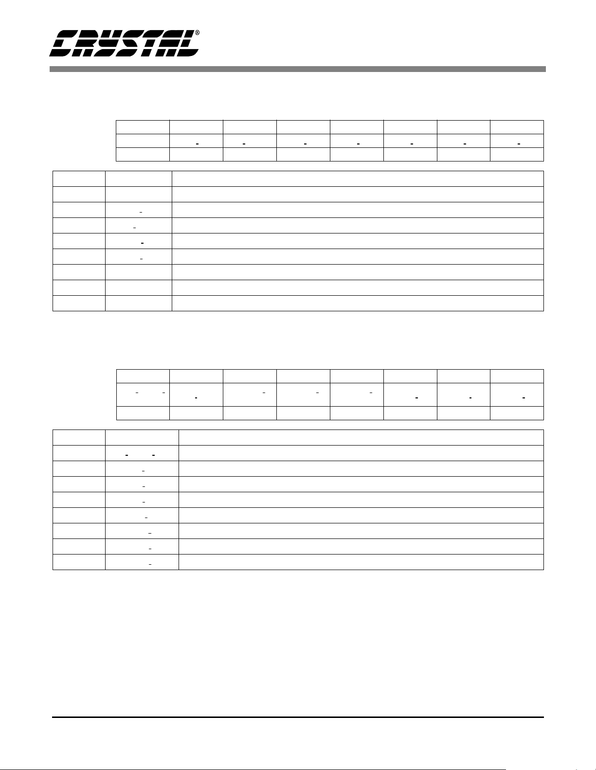
Control Register 5
Address 0×05 CONTROL_5 Read/Write Default Value = 00h
CS4954 CS4955
Bit Number
Bit Name
Default
76543210
RSVD LOW IMP EN COM EN LEN CEN REN GEN B
00000000
Bit Mnemonic Function
76LOW IMP
5EN COM
4EN L
3EN C
2EN_R
1EN_G
0EN_B
reserved
selects between high output impedance (0) or low output impedance (1) mode of DACs
enable DAC for composite output 0: tri-state, 1: enable
enable s-video DAC for luma output 0: tri-state, 1: enable
enable s-video DAC for chroma output 0: tri-state, 1: enable
enable rgb video DAC for red output 0: tri-state, 1: enable
enable rgb video DAC for green output 0: tri-state, 1: enable
enable rgb video DAC for blue output 0: tri-state, 1: enable
Control Register 6
Address 0×06 CONTROL_6 Read/Write Default Value = 00h
Bit Number
Bit Name
Default
76543210
656 SYNC
OUT
00000000
CLIP
OFF
TTXEN
COM2
TTXEN
COM1
TTXEN
SVID
BSYNC
DIS GSYNC DIS RSYNC DIS
Bit Mnemonic Function
7 656 SYNC OUT
6CLIP OFF
5 TTXEN COM2
4 TTXEN COM1
3 TTXEN SVID
2 BSYNC DIS
1 GSYNC DIS
0 RSYNC DIS
Enable (=1) output of hsync and vsync in the ITU R.BT656 mode
Clipping input signals disable (0: clipping active 1: no clipping)
Enable teletext at the composit2 output (0: disable teletext, 1 : enable teletext)
Enable teletext at the composit1 output ( 0: disable teletext, 1 : enable teletext)
Enable teletext at the s-video output ( 0: disable teletext, 1: enable teletext)
Disable syncs in the blue or v output (0: enable syncs, 1: disable syncs)
Disable syncs in the green or u output ( 0: enable syncs, 1: disable syncs)
Disable syncs in the red or y output (0: enable syncs, 1: disable syncs)
DS278PP4 39
Page 40

Background Color Register
Address 0×08 BKG_COLOR Read/Write Default Value = 03h
CS4954 CS4955
Bit Number
Bit Name
Default
76543210
BG
00000011
Bit Mnemonic Function
7:0 BG
Background color (7:5 = R, 4:2 = G, 1:0 = B) (default is 0000 0011 - blue)
GPIO Control Register
Address 0×09 GPIO__REG Read/Write Default Value = 00h
Bit Number
Bit Name
Default
76543210
GPR_CNTRL
00000000
Bit Mnemonic Function
7:0 GPR CNTRL
Input(0)/output(1) control of GPIO registers (bit 0: PDAT(0), bit 7: PDAT(7))
GPIO Data Register
Address 0×0A GPIO_REG Read/Write Default Value = 00h
Bit Number
Bit Name
Default
76543210
GPIO REG
00000000
Bit Mnemonic Function
GPIO data register ( data is output on PDAT bus if appropriate bit in address 09 is
7:0 GPIO REG
set to “1”, otherwise data is input/output through I
2
C mode.
in I
2
C)- This register is only accessible
Sync Register 0
Address 0×0D Sync_0 Read/Write Default Value = 90h
Bit Number
Bit Name
Default
Bit Mnemonic Function
7:3 PROG VS[4:0]
2:0 PROG HS[10:8]
40 DS278PP4
76543210
PROG VS[4:0] PROG HS[10:8]
10010000
programmable vsync lines
programmable hsync pixels (3 most significant bits)
Page 41

Sync Register 1
Address 0×0E Sync_1 Read/Write Default Value = F4h
CS4954 CS4955
Bit Number
Bit Name
Default
76543210
PROG HS[7:0]
11110100
Bit Mnemonic Function
7:0 PROG HS[7:0]
programmable hsync pixels lsb
I2C Address Register
Address 0×0F I2C_ADR Read/Write Default Value = 00h
Bit Number
Bit Name
Default
76543210
RESERVED
00000000
2
I
C ADR
Bit Mnemonic Function
7-
6:0
2
I
C
reserved
I2C device address (programmable)
Subcarrier Amplitude Register
Address 0×10 SC_AMP Read/Write Default Value = 1Ch
Bit Number
Bit Name
Default
76543210
BU AMP
00011100
Bit Mnemonic Function
7:0 BU AMP
Color burst amplitude
Subcarrier Synthesis Register
Address 0×11 SC_SYNTH0 Read/Write Default Value = 3Eh
×12 SC_SYNTH1 F8h
0
×13 SC_SYNTH2 E0h
0
×14 SC_SYNTH3 43h
0
Register Bits Mnemonic Function
SC_SYNTH0 7:0 CC 0
SC_SYNTH1 7:0 CC 1
SC_SYNTH2 7:0 CC 2
SC_SYNTH3 7:0 CC 3
Subcarrier synthesis bits 7:0
Subcarrier synthesis bits 15:8
Subcarrier synthesis bits 23:16
Subcarrier synthesis bits 31:24
DS278PP4 41
Page 42

Hue LSB Adjust Register
Address 0×15 HUE_LSB Read/Write Default Value = 00h
CS4954 CS4955
Bit Number
Bit Name
Default
76543210
HUE LSB
00000000
Bit Mnemonic Function
7:0 HUE LSB
8 LSBs for hue phase shift
Hue MSB Adjust Register
Address 0×16 HUE_MSB Read/Write Default Value = 00h
Bit Number
Bit Name
Default
76543210
RESERVED MSB
00000000
Bit Mnemonic Function
7:2 1:0 HUE MSB
reserved
2 MSBs for hue phase shift
SCH Sync Phase Adjust
Address 0×17 SCH Read/Write Default Value = 00h
Bit Mne monic Function
7:0 SCH
Default - 00h in increments of ≈1.4 degree per bit up to 360°
Closed Caption Enable Register
Address 0×18 CC_EN Read/Write Default Value = 00h
Bit Number
Bit Name
Default
Bit Mnemonic Function
7:2 -
1 CC EN[1]
0 CC EN[0]
765432 1 0
RESERVED EN_284 EN_21
000000 0 0
reserved
enable closed caption for line 284
enable closed caption for line 21
42 DS278PP4
Page 43

Closed Caption Data Register
Address 0×19 CC_21_1 Read/Write Default Value = 00h
×1A CC_21_2 00h
0
×1B CC_284_1 00h
0
×1C CC_284_2 00h
0
Bit Mne monic Function
7:0 CC_21_1
7:0 CC_21_2
7:0 CC_284_1
7:0 CC_284_2
first closed caption databyte of line 21
second closed caption databyte of line 21
first closed caption databyte of line 284
second closed caption databyte of line 284
Wide Screen Signaling Register 0
Address 0×1E WSS_REG_0 Read/Write Default Value = 00h
CS4954 CS4955
Bit Number
Bit Name
Default
Bit Mnemonic Function
7 WSS_23
6 WSS_22
5 WSS_21
4 WSS_20
3 WSS_19
2 WSS_18
1 WSS_17
0 WSS_16
765432 1 0
WSS_23 WSS_22 WSS_21 WSS_20 WSS_19 WSS_18 WSS_17 WSS_16
000000 0 0
Enable wide screen signalling (enable =1)
PAL: enable WSS (enable = 1) on line 23 of field 2,
NTSC: don’t care
PAL: group 4, bit 13, NTSC: don’t care
PAL: group 4, bit 12, NTSC: don’t care
PAL: group 4, bit 11, NTSC: bit 20
PAL: group 3, bit 10, NTSC: bit 19
PAL: group 3, bit 9, NTSC: bit 18
PAL: group 3, bit 8, NTSC: bit 17
DS278PP4 43
Page 44

Wide Screen Signalling Register 1
Address 0×1F WSS_REG_1 Read/Write Default Value = 00h
CS4954 CS4955
Bit Number
Bit Name
Default
765432 1 0
WSS_15 WSS_14 WSS_13 WSS_12 WSS_11 WSS_10 WSS_9 WSS_8
000000 0 0
Bit Mnemonic Function
7 WSS_15
6 WSS_14
5 WSS_13
4 WSS_12
3 WSS_11
2 WSS_10
1 WSS_9
0 WSS_8
PAL: group 2, bit 7, NTSC: bit 16
PAL: group 2, bit 6, NTSC: bit 15
PAL: group 2, bit 5, NTSC: bit 14
PAL: group 2, bit 4, NTSC: bit 13
PAL: group 1, bit 3, NTSC: bit 12
PAL: group 1, bit 2, NTSC: bit 11
PAL: group 1, bit 1, NTSC: bit 10
PAL: group 1, bit 0, NTSC: bit 9
Wide Screen Signalling Register 2
Address 0×20 WSS_REG_2 Read/Write Default Value = 00h
Bit Number
Bit Name
Default
765432 1 0
WSS_7 WSS_6 WSS_5 WSS_4 WSS_3 WSS_2 WSS_1 WSS_0
000000 0 0
Bit Mnemonic Function
7 WSS_ 7
6 WSS_6
5 WSS_5
4 WSS_4
3 WSS_3
2 WSS_2
1 WSS_1
0 WSS_0
PAL: don’t care, NTSC: bit 8
PAL: don’t care, NTSC: bit 7
PAL: don’t care, NTSC: bit 6
PAL: don’t care, NTSC: bit 5
PAL: don’t care, NTSC: bit 4
PAL: don’t care, NTSC: bit 3
PAL: don’t care, NTSC: bit 2
PAL: don’t care, NTSC: bit 1
Filter Register 0
Address 0×22 CB_AMP Read/Write Default Value = 80h
Bit Number
Bit Name
Default
Bit Mnemonic Function
7:0 U_AMP
76543210
U_AMP
10000000
U(Cb) amplitude coefficient
44 DS278PP4
Page 45

Filter Register 1
Address 0×23 CR_AMP Read/Write Default Value = 80h
CS4954 CS4955
Bit Number
Bit Name
Default
Bit Mnemonic Function
7:0 V_AMP
76543210
V_AMP
10000000
V(Cr) amplitude coefficient
Filter Register 2
Address 0×24 Y_AMP Read/Write Default Value = 80h
Bit Number
Bit Name
Default
Bit Mnemonic Function
7:0 Y_AMP
76543210
Y_AMP
10000000
Luma amplitude coefficient
Filter Register 3
Address 0×25 R_AMP Read/Write Default Value = 80h
Bit Number
Bit Name
Default
76543210
R_AMP
10000000
Bit Mnemonic Function
7:0 R_AMP
Red amplitude coefficient
Filter Register 4
Address 0×26 G_AMP Read/Write Default Value = 80h
Bit Number
Bit Name
Default
Bit Mnemonic Function
7:0 G_AMP
DS278PP4 45
76543210
G_AMP
10000000
Green amplitude coefficient
Page 46
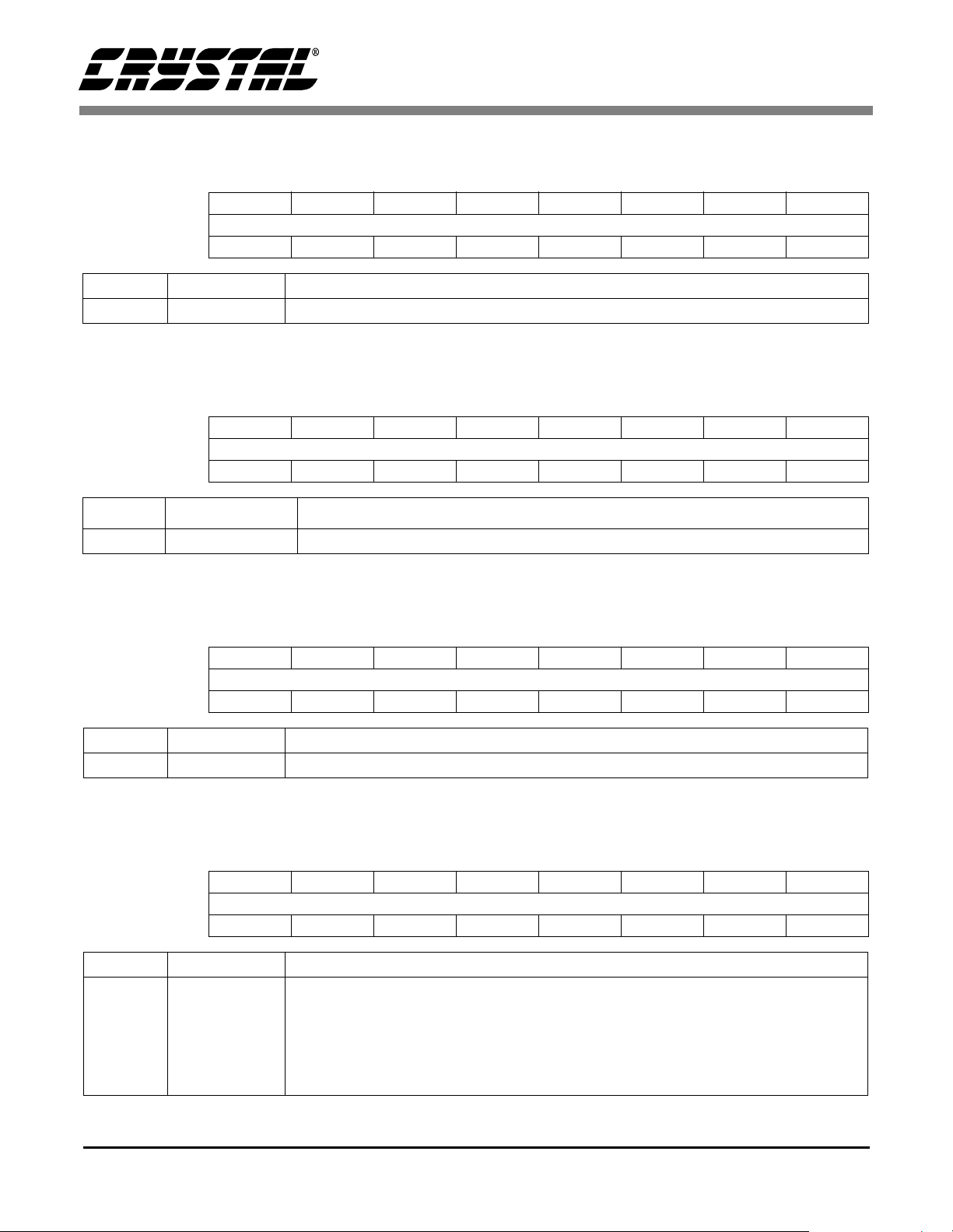
Filter Register 5
Address 0×27 B_AMP Read/Write Default Value = 80h
CS4954 CS4955
Bit Number
Bit Name
Default
Bit Mnemonic Function
7:0 B_AMP
76543210
B_AMP
10000000
Blue amplitude coefficient
Filter Register 6
Address 0×28 Bright_Offsett Read/Write Default Value = 00h
Bit Number
Bit Name
Default
Bit Mnemonic Function
7:0 BRGHT_OFFSET
Teletext Register 0
Address 0×29 TTXHS Read/Write Default Value = A1h
76543210
BRIGHTNESS_OFFSET
00000000
Brightness adjustment ( range: -128 to +127)
Bit Number
Bit Name
Default
Bit Mnemonic Function
7:0 TTXHS
76543210
TTXHS
10100001
Start of teletext request pulses or start of window
Teletext Register 1
Address 0×2A TTXHD Read/Write Default Value = 02h
Bit Number
Bit Name
Default
Bit Mnemonic Function
7:0 TTXHD
76543210
TTXHD
00000010
If TTX_WINDOW = 0 then this register is used as the Pipeline delay between
TTXRQ and TTXDAT signal in the teletext source. User programmable delay step
of 37 ns per LSB.
If TTX_WINDO W = 1 then this register is used a s the 8 LSBs of the te letext in sertion
windows; the 3 MSBs are located in register 0×31. (register 0×31 bit 3)
46 DS278PP4
Page 47
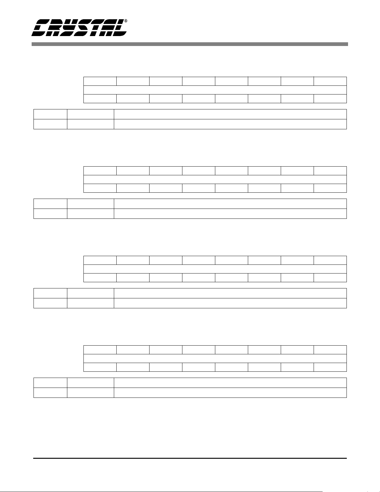
Teletext Register 2
Address 0×2B TTXOVS Read/Write Default Value = 00h
CS4954 CS4955
Bit Number
Bit Name
Default
Bit Mnemonic Function
7:0 TTXOVS
76543210
TTXOVS
00000000
Start of teletext line window in odd field
Teletext Register 3
Address 0×2C TTXOVE Read/Write Default Value = 00h
Bit Number
Bit Name
Default
Bit Mnemonic Function
7:0 TTXOVE
Teletext Register 4
Address 0×2D TTXEVS Read/Write Default Value = 00h
Bit Number
Bit Name
Default
76543210
TTXOVE
00000000
End of teletext line window in odd field
76543210
TTXEVS
00000000
Bit Mnemonic Function
7:0 TTXEVS
Start of teletext line window in even field
Teletext Register 5
Address 0×2E TTXEVE Read/Write Default Value = 00h
Bit Number
Bit Name
Default
Bit Mnemonic Function
7:0 TTXEVE
DS278PP4 47
76543210
TTXEVE
00000000
End of teletext line window in even field
Page 48

Teletext Register 6
Address 0×2F TTX_DIS1 Read/Write Default Value = 00h
CS4954 CS4955
Bit Number
Bit Name
Default
76543210
TTX_LINE_DIS1
00000000
Bit Mnemonic Function
Teletext disable bits corresponding to the lines 5-12 respectively, (11111111=all
7:0 TTX_LINE_DIS1
eight lines are disabled),
(MSB is for line 5, LSB is for line 12)
Teletext Register 7
Address 0×30 TTX_DIS2 Read/Write Default Value = 00h
Bit Number
Bit Name
Default
Bit Mnemonic Function
7:0 TTX_LINE_DIS2
76543210
TTX_LINE_DIS2
00000000
Teletext disable bits corresponding to the lines 13-20 respectively, (11111111=all
eight lines are disablled,
(MSB is for line 13, LSB is for line 20)
Teletext Register 8
Address 0×31 TTX_DIS3 Read/Write Default Value = 00h
Bit Number
Bit Name
Default
Bit Mnemonic Function
7:5 TTXHD
4 Reserved
3 TTX_WINDOW
2:0 TTX_LINE_DIS3
765 4 3 210
TTXHD RESERVED TTX_WINDOW TTX_LINE_DIS3
000 0 0 000
If TTX_WINDOW = 0 these 3 bits are unused.
If TTX_WINDOW = 1 these 3 bits are the MSBs of the register 0×2A; they are used
to specify the length of the teletext insertion window
Selects between TTXRQ (= 0) pulsation or TTXRQ (= 1) Window mode
Teletext disable bits corresponding to the lines 13-20 respectively, (111=all three
lines are disabled),
(MSB is for line 21, LSB is for line 23)
48 DS278PP4
Page 49

Interrupt Register 0
Address 0×32 INT_EN Read/Write Default Value = 00h
CS4954 CS4955
Bit Number
Bit Name
Default
76543 2 1 0
RESERVED INT_21_EN INT_284_EN INT_V_EN
00000 0 0 0
Bit Mnemonic Function
7:3 -
2 INT_21_EN
1 INT_284_EN
0INT_V_EN
reserved
interrupt enable for closed caption line 21
interrupt enable for closed caption line 284
interrupt enable for new video field
Interrupt Register 1
Address 0×33 INT_CLR Read/Write Default Value = 00h
Bit Number
Bit Name
Default
Bit Mnemonic Function
7:3 -
2 CLR_INT_21
1 CLR_INT_284
0 CLR_INT_V
76543 2 1 0
RESERVED CLR_INT_21 CLR_INT_284 CLR_INT_V
00000 0 0 0
reserved
clear interrupt for closed caption line 21 (INT 21)
clear interrupt for closed caption line 284 (INT_284)
clear interrupt for new video field (INT_V)
Status Register 0
Address 0×34 STATUS_0 Read Only Def ault Value = 00h
Bit Number
Bit Name
Default
543 2:0
INT_21 INT_284 INT_V FLD
000 0
Bit Mnemonic Function
5INT_21
4 INT_284
3INT_V
2:0 FLD_ST
Interrupt flag for line 21 (closed caption) complete
Interrupt flag for line 284 (closed caption) complete
Interrupt flag for video field change
Field Status bits(001 = field 1,000 = field 8)
Status Register 1
Address 0×5A STATUS_1 Read only Default Value = 04h
Bit Number 76543210
Bit Name
Default
00000100
Bit Mnemonic Function
7:0 DEVICE_ID
Device identification: CS4954: 0000 0100, CS4955: 0000 0101
DEVICE_ID
DS278PP4 49
Page 50

CS4954 CS4955
9. BOARD DESIGN AND LAYOUT CONSIDERATIONS
The printed circuit layout should be optimized for
lowest noise on the CS4954/5 placed as close to the
output connectors as possible. All analog supply
traces should be as short as possible to minimize inductive ringing.
A well designed power distribution network is essential in eliminating digital switching noise. The
ground planes must provide a low-impedance return path for the digital circuits. A PC boa rd with a
minimun of four layers is recommended. The
ground layer should be used as a shield to isolate
noise from the analog traces. The top layer (1)
should be reserved for analog traces but digital
traces can share this layer if the digital signals have
low edge rates and switch little current or if they are
separated from the analog traces by a signigicant
distance (dependent on their frequency content and
current). The second layer should then be the
ground plane followed by the analog power plane
on layer three and the digital signal layer on layer
four.
9.1. Power and Ground Planes
The power and ground planes need isolation gaps
of at least 0.05" to minimize digital switching noise
effects on the analog signals and components. A
split analog/digital ground plane should be connected at one point as close as possible to the
CS4954/5.
9.2. Power Supply Decoupling
Start by reducing power supply ripple and wiring
harness inductance by placing a large (33-100 uF)
capacitor as close to the power entry point as possible. Use separate power planes or traces for the
digital and analog sections even if they use the
same supply. If necessary, further isolate the digital
and analog power supplies by using ferrite beads on
each supply branch followed by a low ESR ca pacitor.
Place all decoupling caps as close as possible the
the device as possible. Surface mount capacitors
generally have lower inductance than radial lead or
axial lead components. Surface mount caps should
be place on the component side of the PCB to minimize inductance caused by board vias. Any vias,
especially to ground, should be as large as possible
to reduce their inductive effects.
9.3. Digital Interconnect
The digital inputs and outputs of the CS4954/5
should be isolated from the analog outputs as much
as possible. Use separate signal layers whenever
possible and do not route digital signals over the
analog power and ground planes.
Noise from the digital section is related to the digital edge rates used. Ringing, overshoot, undershoot, and ground bounce are all related to edge
rate. Use lower speed logic such as HCMOS for the
host port interface to reduce switching noise. For
the video input ports, higher speed logic is required, but use the slowest practical edge rate to reduce noise. To reduce noise, it is important to
match the source impedance, line impedance, and
load impedance as much as possible. Generally, if
the line length is greater than one fourth the signal
edge rate, line termination is necessary. Ringing
can also be reduced by damping the line with a series resistor (22-150 Ω). Under extreme cases, it
may be advisable to use microstrip techniques to
further reduce radiated switching noise if very fast
edge rates (<2ns) are used. If microstrip techniques
are used, split the analog and digital ground planes
and use proper RF decoupling techniques.
9.4. Analog Interconnect
The CS4954/5 should be located as close as possible the output connectors to minimize noise pickup
and reflections due to impedance mismatch. All unused analog outputs should be placed in shutdown.
This reduces the total power that the CS4954/5 requires, and eliminates the impedance mismatch
50 DS278PP4
Page 51

CS4954 CS4955
presented by an unused connector. The analog outputs should not overlay the analog power plane to
maximize high frequency power supply rejection.
9.5. Analog Output Protection
To minimize the possibility of damage to the analog output sections, make sure that all video connectors are well grounded. The connector should
have a good DC ground path to the analog and digital power supply grounds. If no DC (and low frequency) path is present, improperly grounded
equipment can impose damaging reverse currents
on the video out lines. Therefore, it is also a good
idea to use output filters that are AC coupled to
avoid any problems.
9.6. ESD Protection
All MOS devices are sensitive to Electro Static
Discharge (ESD). When manipulating these devices, proper ESD precautions are recommended to
avoid performance degradation or permanent dramage.
9.7. External DAC Output Filter
If an output filter is required, the low pass filter
shown in Figure 30 can be used.
2.2µH
C
1
C
330pF 220pF
Figure 30. External Low Pass Filter
should be chosen so that C1 = C2 + C
2
OUTIN
C
2
cable
DS278PP4 51
Page 52

Vcc
L1
Ferrite Bead
4.7 µF
CS4954 CS4955
0.1 µF
1.5 kΩ
I2C
Controller
27 MHz Clock
Gpio port
Vcc
Pixel Data
NC
1.5 kΩ
110
110
30
31
26-19
Ω
Ω
8-1
15
14
16
27
28
32
33
29
8
XTALIN
XTALOUT
PADDR
TTXDAT
TTXRQ
PDAT[7:0]
RD
WR
SDA
SCL
CLK
V[7:0]
17 36 41
VDD
CS4954
CS4955
46
VAA
VREF
RED
GREEN
BLUE
CVBS
38
39
40
43
75 or
300 Ω
44
75 or 300 Ω
48
Y
47
C
75 or 300 Ω
S-Video
Connector
75 or
300 Ω
75 or
300 Ω
Composite
Connector
to SCART
Connector
Video
9
10
11
13
FIELD
HSYNC
VSYNC
TEST
/CB
/CB
GNDD
GNDA
18 34 42 45
INT
RESET
ISET
12
34
37
75 or 300 Ω
4kΩ±1%
Figure 31. Typical Connection Diagram
52 DS278PP4
Page 53

10. PIN DESCRIPTION
CS4954 CS4955
CVBS
GNDA
VAA
V0
V1
V2
V3
V4
V5
V6
V7
FIELD /CB
HSYNC
/CB
VSYNC
INT
TEST
XTAL_OUT
XTAL_IN
PADR
VDD
GNDD
B
GNDA
VAA
G
R
C
Y
48 47 46 45 44 43 4142 40 39 38 37
1
2
3
4
5
6
7
8
9
10
11
12
13 14 15 16 17 18 2019 21 22 23 24
CS4954-CQ
CS4955-CQ
48-Pin TQFP
Top View
36
35
34
33
32
31
30
29
28
27
26
25
VREF
ISET
VAA
GNDA
RESET
SCL
SDA
TTXRQ
TTXDAT
CLKIN
WR
RD
PDAT0
PDAT1
PDAT2
PDAT3
PDAT4
PDAT5
PDAT6
PDAT7
DS278PP4 53
Page 54

CS4954 CS4955
Pin Name Pin Number Type Description
V [7:0] 8, 7, 6, 5, 4, 3, 2, 1 IN Digital video data inputs
CLK 29 IN 27 MHz input clock
PADDR 16 IN Address enable line
XTAL_IN 15 IN subcarrier crystal inpu t
XTAL_OUT 14 OUT subcarrier crystal output
HSYNC
VSYNC
FIELD/CB 9 OUT Video field ID. Selectable polarity or composite blank
RD
WR
PDAT [7:0] 19, 20, 21, 22, 23, 24, 25, 26 I/O Host parallel port/ general purpose I/O
SDA 32 I/O I
SCL 33 IN I
CVBS 44 CURRENT Composite video output
Y 48 CURRENT Luminance analog output
C 47 CURRENT Chrominance ana log output
R 39 CURRENT Red analog output
G 40 CURRENT Green analog output
B 43 CURRENT Blue analog output
VREF 38 I/O Internal voltage reference output or external refer-
ISET 37 CURRENT DAC current set
TTXDAT 30 IN Teletext data input
TTXRQ 31 OUT Teletext request output
INT 12 OUT Interrupt output, active high
RESET
TEST 13 IN TEST pin. Ground for normal operation
VAA 36, 41, 46 PS + 5 V or + 3.3 V supply (must be same as VDD)
GNDD 18 PS Ground
VDD 17 PS +5 V or 3.3 V supply (must be same as VAA)
GNDA 35, 42, 45 PS Ground
/CB
10 I/O Active low horizontal sync, or composite blank signal
11 I/O Active low vertical sync.
27 IN Host parallel port read strobe, active low
28 IN Host parallel port write strobe, active low
2
C data
2
C clock input
ence input
34 IN Acti ve low master RESET
Table 10. Device Pin Description
54 DS278PP4
s
Page 55

11. PACKAGE DRAWING
48L TQFP PACKAGE DRAWING
D1
D
CS4954 CS4955
E
E1
1
e
B
∝
L
INCHES MILLIMETERS
DIM MIN MAX MIN MAX
A --- 0.063 --- 1.60
A1 0.002 0.006 0.05 0.15
B 0.007 0.011 0.17 0.27
D 0.343 0.366 8.70 9.30
D1 0.272 0.280 6.90 7.10
E 0.343 0.366 8.70 9.30
E1 0.272 0.280 6.90 7.10
e* 0.016 0.024 0.40 0.60
L 0.018 0.030 0.45 0.75
∝ 0.000° 7.000° 0.00° 7.00°
* Nominal pin pitch is 0.50 mm
A
A1
Controlling dimension is mm.
JEDEC Designation: MS026
DS278PP4 55
Page 56

 Loading...