

CS4952/53
T
NTSC/PAL Digital Video Encoder
Features
l
Simultaneous composi t e and S-video output
l
Supports RS170A and CCIR601 composite
output timing
l
Multi-standard support for NTSC-M, PAL (B, D,
G, H, I, M, N, Combination N)
l
Optional progre ssive scan @ M PEG2 field ra tes
l
CCIR656 input mode supporting EAV/SAV
codes and CCIR601 Master/Slave i nput modes
l
Stable color subcarrier for MPEG2 systems
l
NTSC closed caption enc oder with inte rrupt
l
Supports Macrovision copy protection in
CS4953 version
l
Host interfac e c onfigurable fo r parallel or I2C
compatible operation
l
General pur pose input and output pins
l
Individual DAC power-down capabilit y
l
On-chip vol ta ge reference generator
l
On-chip col or bar generato r
l
+5 volt only, CMOS, low power modes, tri-sta te
DACs
Description
The CS4952/3 provides full conversion from YCbCr or
YUV digital video formats into NTSC & PAL Composite
and Y/C (S-video) analog video. Input formats can be
27 MHz 8-bit YUV, 8-bit YCbCr, or CCIR656 with support for EAV/SAV codes. Output video can be form atted
to be compatible with NTSC-M, or PAL B,D,G,H,I,M,N,
and Combination N systems. Also supported is NTSC
line 21 and line 284 closed captioning encoding.
Four 9-bit DACs provide two channels for an S-Video output port and two composite video outputs. 2x oversampling
reduces the output filter requirements and guarantees
no DAC related modulation co mponents within the specified bandwidth of any of the suppor ted video standards.
Parallel or high speed I
are provided for flexibility in system design. The parallel
interface doubl es as a general pu rpose I/O port when t he
CS4952/3 is in I
board area.
ORDERING INFORMATION
CS4952/3-CL 44 pin PLCC
CS4952/3-CQ 44 pin TQFP
2
C compat ible con trol int erfac es
2
C mode to help conserve valuable
CLK
SCL
SDA
PDAT[7:0]
RD*
WR*
ADDR
XTAL
VD[7:0]
HSYNC*
VSYNC*
FIELD
INT
RESET*
2
I C
Interface
8
Host
Parallel
Interface
Color Sub-carrier
Synthesizer
8
Formatter
Video Timing
Generator
Preliminary Product Information
Cirrus Logic, Inc.
Crystal Semiconductor Products Division
P.O. Box 17847, Austin, Texas 78760
(512) 445 7222 FAX: (512) 445 7581
http://www.crystal.com
VAA
LPF
LPF
9-Bit
DAC
9-Bit
Σ
DAC
9-Bit
DAC
9-Bit
DAC
Voltage
Reference
Current
Reference
C
CVBS37
CVBS75
Y
VREFIN
VREFOU
ISET
Video
Control
Registers
Output
Interpolat e
Chroma Amplifier
Chroma Modulate
Burst Insert
Chroma I n terpolate
LPF
U, V
Y
Luma Delay
Luma Amplifier
Sync Insert
Output
Interpolate
GND TEST
This document contains information for a new product.
Cirrus Logic reserves the right to modify this product without notice.
Copyright Cirrus Logic, I nc. 1997
(All Rights Reserv ed)
OCT ‘97
DS223PP2
1

TABLE OF CONTENTS
AC & DC PARAMETRIC SPECIFICATIONS .....................................................................4
INTRODUCTION ...............................................................................................................11
FUNCTIONAL DESCRIPTION .........................................................................................11
Video Timing Generator .........................................................................................11
Video Input Formatter .............................................................................................11
Color Subcarrier Synthesizer ..................................................................................12
Chroma Path ..........................................................................................................12
Luma Path ........................................ ........ ......... ........ ........ ......... ........ ......... ...........12
Digital to Analog Converters ...................................................................................13
Voltage Reference ..................................................................................................13
Current Reference ..................................................................................................13
Host Interface .........................................................................................................13
Closed Caption Services ........................................................................................ 13
Control Registers ....................................................................................................13
OPERATIONAL DESCRIPTION .......................................................................................14
Reset Hierarchy ......................................................................................................14
Video Timing ...........................................................................................................14
Slave Mode Input Interface .............................................................................14
Master Mode Input Interface ...........................................................................14
Vertical Timing .................................................................................................15
Horizontal Timing ............................................................................................15
NTSC Interlaced ..............................................................................................17
PAL Interlaced .................................................................................................17
Progressive Scan ............................................................................................19
PAL Progressive Scan ....................................................................................19
NTSC Progressive Scan .................................................................................19
CCIR-656 ................................................................................................................19
Digital Video Input Modes .......................................................................................22
Multi-standard Output Format Modes .....................................................................22
Subcarrier Generation ............................................................................................22
Subcarrier Compensation .......................................................................................22
Closed Caption Insertion ........................................................................................23
Color Bar Generator ...............................................................................................23
Interrupts ................................................................................................................24
General Purpose I/O Port .......................................................................................24
ANALOG ...........................................................................................................................24
Analog Timing .........................................................................................................24
VREF ......................................................................................................................25
ISET ........................................................................................................................25
DACs ......................................................................................................................25
Luminance DAC ..............................................................................................25
Chrominance DAC ... ........ ......... ........ ......... .......................................... ........ ...25
CVBS75 DAC ..................................................................................................26
CVBS37 DAC ..................................................................................................26
PROGRAMMING ..............................................................................................................27
Host Control Interface .............................................................................................27
I2C Interface ....................................................................................................27
8-bit Parallel Interface .....................................................................................27
Register Description ................................. ......... ........ ........ ......... ........ ......... ........ ...28
Control Register 0............................................................................................28
Control Register 1............................................................................................29
Control Register 2............................................................................................30
DAC Power Down Register..............................................................................30
Status Register.................................................................................................31
Background Color Register..............................................................................31
GPIO Control Register ......................................................... ........ ......... ........ ...31
GPIO Data Register .. ........ ......... .......................................... ........ ......... ........ ...32
Chroma Filter Register.....................................................................................32
Luma Filter Register............................................ ........ ......... ........ ......... ........ ...32
I2C Address Register.......................................................................................32
Subcarrier Amplitude Register .........................................................................33
CS4952/53
2 DS223PP2

Subcarrier Synthesis Register .........................................................................33
Hue LSB Adjust Register.................................................................................33
Hue MSB Adjust Register................................................................................33
Closed Caption Enable Register......................................................................34
Closed Caption Data Register.........................................................................34
Interrupt Enable Register.................................................................................34
Interrupt Clear Register....................................................................................35
Device ID Register...........................................................................................35
BOARD DESIGN & LAYOUT CONSIDERATIONS .........................................................36
Power and Ground Planes .....................................................................................36
Power Supply Decoupling ......................................................................................36
VREF Decoupling ...................................................................................................36
Digital Interconnect ................................................................................................36
Analog Interconnect ...............................................................................................37
Analog Output Protection .......................................................................................37
ESD Protection .......................................................................................................37
External DAC Output Filter .....................................................................................37
DEVICE PINOUT - 44 PLCC ............................................................................................38
PLCC Pin Description ............................................................................................39
DEVICE PINOUT - 44 TQFP ............................................................................................41
TQFP Pin Description ............................................................................................42
CS4952/53
DS223PP2 3
CS4952/53
AC & DC PARAMETRIC SPECIFICATIONS
ABSOLUTE MAXIMUM RATINGS: (AGND, DGND = 0 V, all voltages with respect to 0 V.)
Parameter Symbol Min Max Units
Power Supply
Input Current Per Pin Except Supply Pins -10 10 mA
Output Current Per Pin Except Supply Pins -50 +50 mA
Analog Input Voltage -0.3
Digital Input Voltage -0.3
Ambient Temperatur e Power Applied -55 +125 °C
Storage Temperature -65 +150 °C
Warning: Operating beyond these limits may result in permanent damage to the device.
Normal operation is not guarant eed at these extremes.
RECOMMENDED OPERATING CONDITI ONS: (AGND, DGND = 0 V, all voltages with
respect to 0 V.)
V
AA
-0.3 6.0 V
V
+0.3
AA
VAA+0.3
V
V
Parameter Symbol Min TypMax Units
Power Supplies: Digital Analog
Operating Ambient Temperature
V
AA
T
A
4.75 5.0 5.25 V
0+25+70 °C
4 DS223PP2
CS4952/53
D.C. CHARACTERISTICS: (T
=25 C; VAA = 5 V; GND = 0 V.)
A
Parameter Symbol Min T yp Max Units
Digital Inputs
High Level Input Voltage V [7:0], PDAT [7:0],
HSYNC
High Level Input Voltage I
/VSYNC/FIELD/CLKIN
2
Low Level Input Voltage All Inputs
V
IH
V
C
IH
V
IL
2.0 -
0.7V
AA
--V
-0.3 - 0.8 V
VAA+0.3
Input Leakage Current Digital Input s - -10 - +10
Digital Outputs
High Level Output Voltage Io = -4mA
Low Level Output Voltage Io = 4mA
Low Level Output Voltage SDA pin only, Io = 6mA
V
OH
V
OL
V
OL
2.4 -
--0.4V
--0.4V
V
AA
Output Leakage Current High-Z Digital Outputs - -10 - +10
Analog Outputs
Full Scale Output Current CVBS37/Y/C (Note 1) IO37 32.9 34.7 36.5 mA
Full Scale Output Current CVBS75 (Note 1) IO75 16.4 17.3 18.2 mA
LSB Current CVBS37/Y/C (Note 1) IB37 64.5 68 71.5
LSB Current CVBS75 (Note 1) IB35 32.2 34 35.8
DAC-to-DAC Matching MAT - 2 - %
R
C
O
V
OUT
OUT
T
OC
DEL
RF
0-+1.4V
-15-k
--30pF
-412ns
-2.55ns
Output Compliance
Output Impedance
Output Capacitance
DAC Output Delay
DAC Rise/Fall Time (Note 2)
Voltage Reference
Reference Voltage Output
Reference Input Current
V
OV
I
VC
1.198 1.232 1.272 V
--10
Power Supply
Supply Voltage
Supply Current All DACs on
CVBS75/CVGS37 only
CVBS75 only
V
AA
IAA1
IAA2
IAA3
4.75 5 5.25 V
-
-
-
180
110
75
200
-
-
mA
mA
mA
V
µ
A
V
µ
A
µ
A
µ
A
Ω
µ
A
Notes: 1. Output current level s with ISET = 10 kΩ, VREFIN = 1.232 V.
2. Times for black-to-white level and white-to-bl ack level transitions.
DS223PP2 5
CS4952/53
D.C. CHARACTERISTICS (Continued)
Parameter Symbol Min Typ Max Units
Static Performan c e
DAC Resolution - - 9 Bits
Differential Non-Line arity DNL -1 ±0.5 +1 LSB
Integral Non-Linearity INL -1 ±0.35 +1 LSB
Dynamic Performance
Differential Gain DB - 2 5 %
Differential Phase DP - ±0.5 ±2 °
Signal to Noise Ratio SNR -70 - - dB
Hue Accuracy
Saturation Accuracy
H
A
S
A
--2°
--2%
6 DS223PP2

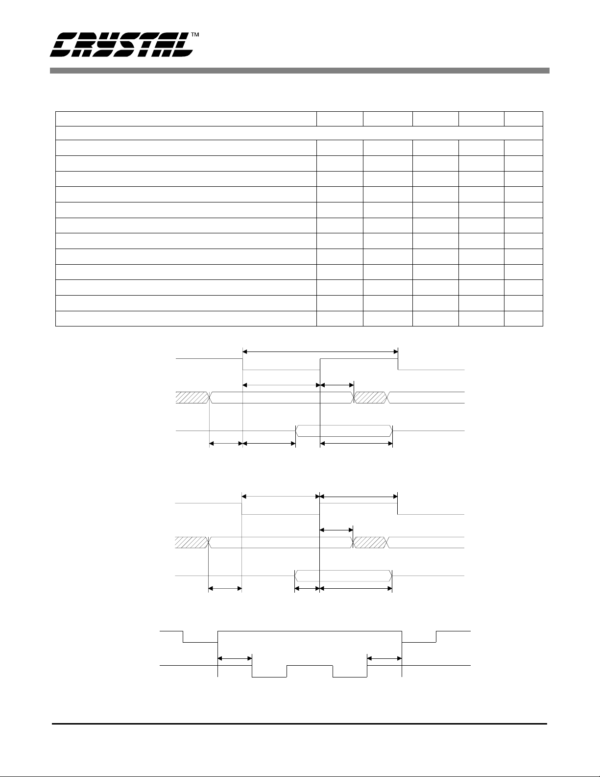
A.C. CHARACTERISTICS:
Parameter Symbol Min Typ Max Units
Pixel Input and Control Port
Clock Pulse High Time
Clock Pulse Low Time
Clock to Data Set-up Time
Clock to Data Hold Time
Clock to Data Output Delay
CLK
TchT
V[7:0]
HSYNC*/VSYNC*
(Inputs)
HSYNC*/VSYNC*/
CB/FIELD/INT
(Outputs)
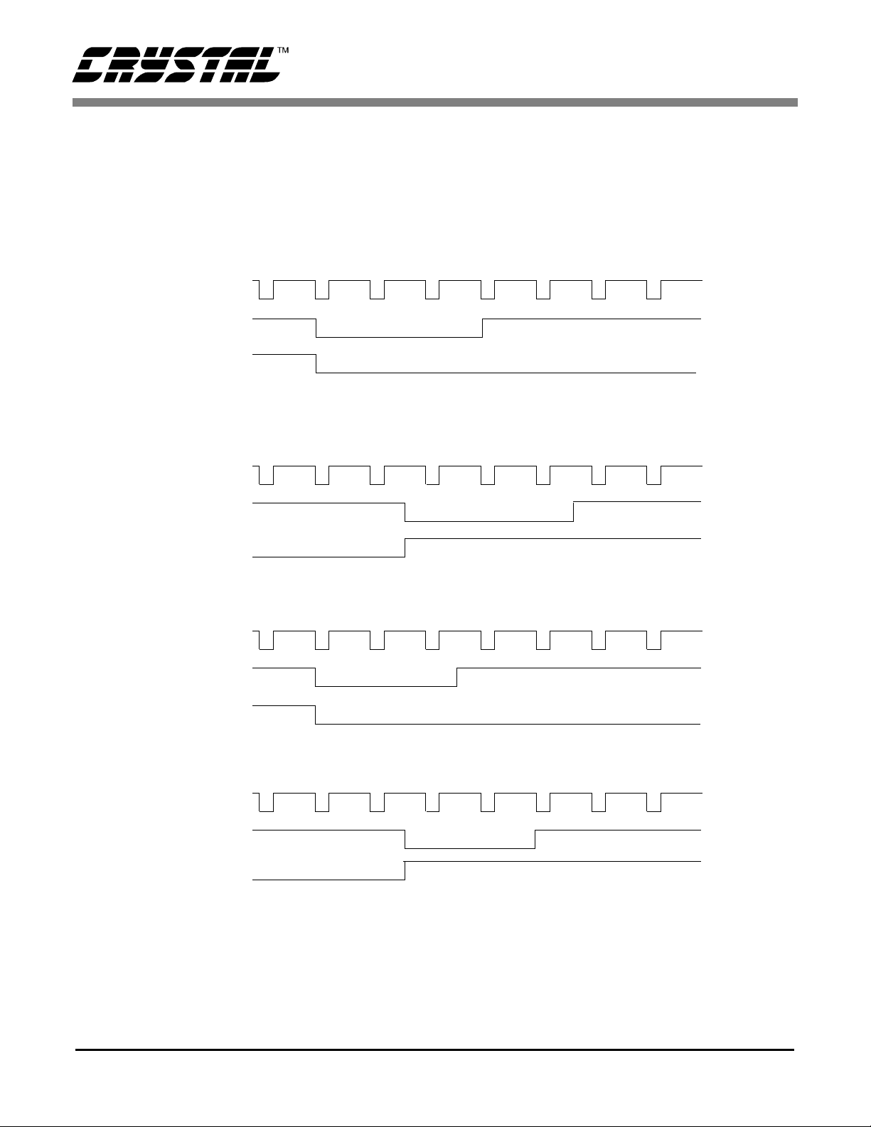
Figure 1. Video Pixel Data and Control Port Timing
CS4952/53
T
ch
T
cl
T
isu
T
ih
T
oa
T
cl
isu
T
ih
14.82 18.52 22.58 ns
14.82 18.52 22.58 ns
6--ns
0--ns
--17ns
T
oa
Parameter Symbol Min Typ Max Units
I2C Host Port Timing
SCL Frequency
Clock Pulse High Time
Clock Pulse Low Time
Hold Time (Start Condition)
Setup Time (Start Condition)
Data Setup Time
Rise Time
Fall Time
Setup Time (Stop Condition)
Bus Free Time
Data Hold Time
SCL Low to Data Out Valid
SDA
SCL
F
clk
T
sph
T
spl
T
sh
T
ssu
T
sds
T
sr
T
sf
T
ss
T
buf
T
dh
T
vdo
T
T
sh
buf
T
sr
T
sph
T
T
sds
dh
T
vdo
100 1000 KHz
0.1 µs
0.7 µs
100 ns
100 ns
50 ns
1µs
0.3 µs
100 ns
100 ns
0ns
600 ns
T
sh
T
ss
T
spl
T
sf
T
ssu
Figure 2. I2C Host Port Timing
DS223PP2 7
A.C. CHARACTERISTICS: (Continued)
Parameter Symbol Min Typ Max Units
8-bit Parallel Host Interface
Read Cycle Time
Read Pulse Width
Address Setup Ti me
Read Address Hold Time
Read Data Access Time
Read Data Hold Time
Write Recovery Time
Write Pu lse Width
Write Data Setup Time
Write Data Hold Time
Write-Read/Read-Write Recovery Time
Address from Write Hold Time
T
T
T
T
T
T
T
T
T
T
T
wpw
wds
wdh
T
wac
rd
rpw
as
rah
rda
rdh
wr
rec
CS4952/53
60 - - ns
30 - - ns
3--ns
10 - - ns
--40ns
10 - 50 ns
60 - - ns
40 - - ns
8--ns
3--ns
50 - - ns
0--ns
RD*
ADDR
PDAT[7:0]
WR*
ADDR
PDAT[7:0]
T
rd
T
rpw
T
as
T
rda
T
rah
T
rdh
8-bit Parallel Host Port Timing: Read Cycle
T
wpw
T
as
T
wds
T
wr
T
wac
T
wdh
8-bit Parallel Host Port Timing: Address Write Cycle
WR*
T
rec
RD*
T
rec
8-bit Parallel Host Port Timing: Read-Write/Write-Read Cycle
Figure 3.
8 DS223PP2
A.C. CHARACTERISTICS: (Continued)
Parameter Symbol Min Typ Max Units
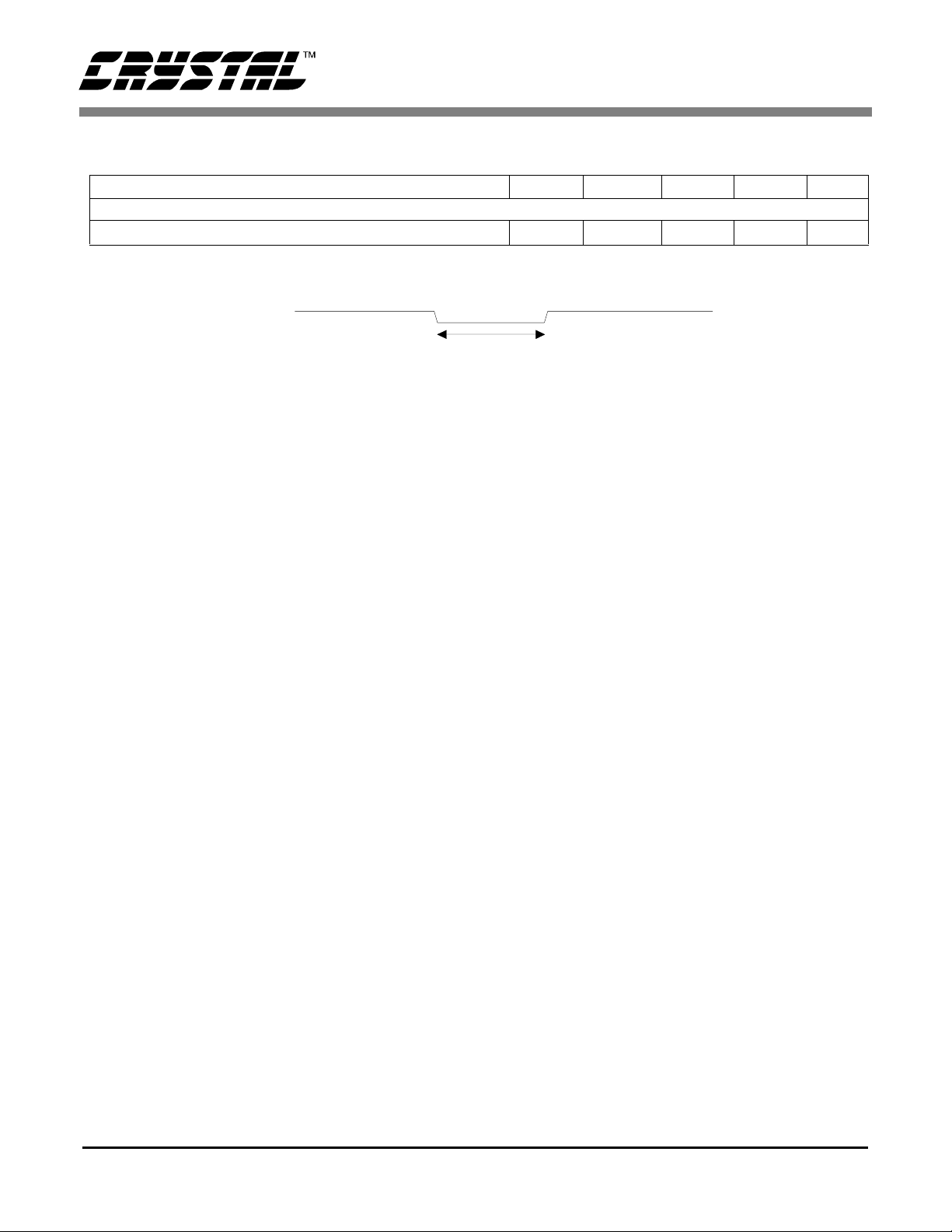
Reset Timing
Reset Pulse Width
RESET*
Figur e 4. Reset Timing
CS4952/53
T
res
T
res
100 ns
DS223PP2 9
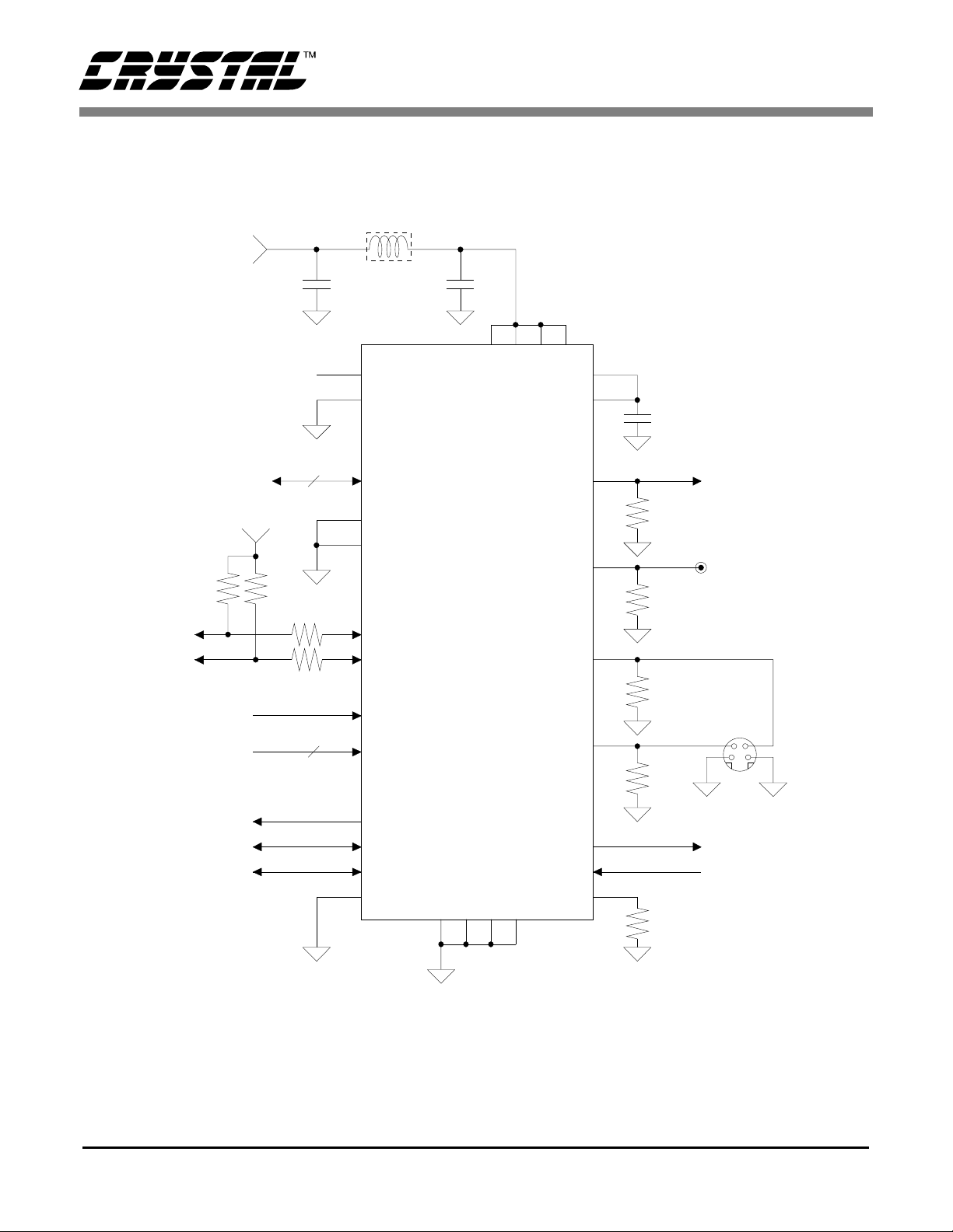
+5V
(Vcc)
L1
Ferrite Bead
4.7 µF 0.1 µF
18
NC
19
XTAL
ADDR
1
3
VAA
VREFOUT
20 29
VREFIN
42
41
CS4952/53
0.1 µF
2
I C
Controller
27 MHz Clock
GPIO Port
+5V (Vcc)
Ω
1.5k
Pixel Data
1.5k
Ω
110
110
8
Ω
Ω
8
31
32
35
36
33
7-14
15
16
17
PDAT[7: 0]
RD*
WR*
SDA
SCL
CLK
V[7:0]
FIELD
HSYNC*/CB
VSYNC*
6
TEST
CS4952
CS4953
GND
2 21 22
CVBS75
CVBS37
RESET*
38
INT
ISET
5
75
4
75
43
Y
75
44
C
75
34
37
40
10 kΩ±1%
To RF Modulator
Ω
Composite Video
Connector
Ω
Ω
S-Video
Connector
Ω
Figure 5. Typical Connection Diagram (I2C host interface)
10 DS223PP2

CS4952/53
INTRODUCTION
The CS4952/3 is a co mp lete mult i-stan dard dig ital
video enco der implem ented in current 5-volt only
CMOS technology. CCIR601 or CCIR656 compliant digital video input can be converted into
NTSC-M, PAL B, PAL D, PAL G, PAL H, PAL I,
PAL M, PAL N, or PAL N A rgentina- compatib le
analog vide o. Th e CS49 52/ 3 is de sig ned to conn ect
to MPEG1 and MPEG2 dig ital video decompressors without glue logic .
Two 9-bit DAC outputs provide high quality
S-Video analog output while two other 9-bit DACs
simultaneously generate composite analog video.
The CS4952/3 will accept 8-bit YCbCr or 8-bit
YUV input data.
The CS495 2/3 is completely con figured and con-
2
trolled via an 8-bit host interface port or an I
compatible serial interface. This host port provides
access and control of all CS4952/3 options and features like closed caption insertion, interrupts, etc.
In order to lo wer the en d user set- top overall s ystem costs, the CS4 952/3 provide s an inter nal volt age reference which eliminates the requirement for
an external disc re te 3-pin voltage reference.
C
FUNCTIONAL DESCRIPTION
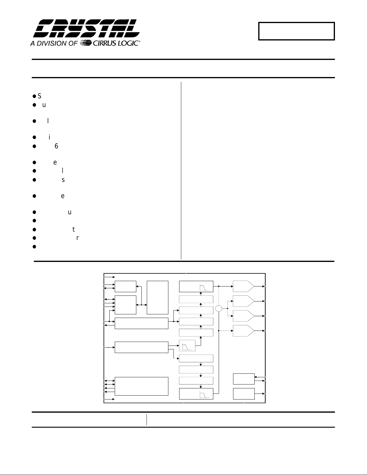
In the following subse ctions, the functi ons of the
CS4952/3 will be described. The descriptions refer
to the block diagram on the cover page.
Video Timing Generator
All timing generation is accomplished via a
27 MHz input applied to the CLK pin. The
CS4952/3 can also accept an opti onal color burst
crystal on the ADDR & XTAL pins. See section:
Color Subcarrier Synthesizer (page 12), for further
details.
The Video Ti mi ng Generator is responsible for orchestrating most all of th e other modules in th e device. It wor ks i n harmony wi th external sync input
timing or by providing external sync timing out-
puts. It automatically disables color burst on appropriate scan lines and generates serration and
equalization pulses on appropriate sca n li nes.
The CS4952/ 3 is designed to function a s a video
timing master or video timing slave. In both Master
and Slave Modes, all timing is sampled and asserted with the rising edge of the CLK pin.
In most cases the CS495 2/3 will serve as the vi deo
timing master. The master timing cannot be externally altere d other than through the host interface
by changing the video display modes: PAL or
NTSC and Progressive Scan. HSYNC
and FIELD are configured as outputs for Master
Mode. HSYNC
blanking output signal in Mast er Mode. Exact horizontal and vertical displ ay timing is a ddressed in
section: Operati ona l De scription (page 14).
In Slave Mode HSYN C
ured as input pins and are used to initialize inde pendent vertical and horizontal timing generators
upon their respective falling edges. FIELD remains
an output in Slave Mode.
The CS4952/3 also provides a CCIR-656 Slave
Mode where the video inpu t stream c ontains EAV
and SAV codes. In this case, proper HSYNC
VSYNC timing is extracted automatically without
aid from any inputs other than the V [7:0].
CCIR-656 input data is sampled with th e leading
edge of C LK. Slave M ode vertical an d horizontal
timing derived via CCIR-656 or ext er na l ha rdware
must be equivalent to timing generated by the
CS4952/3 in Master Mode .
can also be defined as a composite
and VSYNC are config-
, VSYNC
Video Input Formatter
The video input form atter translates YCbCr input
data into YUV information, if necessary, and splits
the luma and chroma information for filtering, scaling, and modulation.
DS223PP2 11

CS4952/53
Color Subcarrier Synthesizer
The subcarrier synthesizer is a digital frequency
synthesizer that produces the correct subcarrier frequency for NTSC or PAL. The CS4952/3 generates
the color burst fre quency based on the input CLK
(27 MHz). Color burst accuracy and stability are
limited by the accuracy of the 27 MHz input. If the
frequency varies then the color burst frequency will
also vary accordi ngl y.
In order to handle situations in which the CLK varies unacceptably, a local crystal frequency reference may be used on the ADDR & X TAL device
pins. In this instance the input CLK is continuously
compared with the external crystal reference input
and the internal timing of the CS4952/3 is auto matically adjusted so that the color burst frequency remains close to the requirements.
Controls are pr ovided for phase ad justment of the
burst to permit color adjustment and phase compensation. C hroma hue c ontrol is pro vided by t he
CS4952/3 via a 10-bit Hue Control Register
(HUE_LSB and H_MSB). Burst amplitude control
is also made available to the host via the 8-bit burst
amplitude register (SC_AMP).
The output of the chroma low pass filter is connected to the c hro ma i nterp ol atio n filt er whe re upsam pling from 4:2:2 to 4:4:4 is accomplished. The
chroma digital data is fed to a quadrature modulator
where they are combined with the output from the
subcarrier synthesizer to produce the proper modulated chrominance signal.
Following chroma modulation the chroma data
passes through a vari able gai n amp lifi er w here t he
chroma amp litude may be varied via th e C_AMP
8-bit host addressa ble re giste r. Th e c hroma then i s
interpola ted by a fact or of 2 in orde r to operate the
output DACs at 2 times the pixel rate. The interpolated filters help reduce the sinx/x roll-off for higher frequencies and reduce the complexity of the
external ana log low pa ss filte rs.
Luma Path
Along with the chr oma output pat h, the CS495 2/3
Video Input Formatter initiates a parallel luma data
path by d irecting the luma data to a digital delay
line. The delay line is built as a digital FIFO where
the depth of the FIFO repl icates the cloc k period
delay associated with the more complex chroma
path.
Chroma Path
The Video Input Formatter a t conclusion deli vers
4:2:2 YUV o u tputs into se parate chro ma and lum a
data paths. The chroma path will be discussed here.
The chroma output of the Video Input Formatter is
directed to a chroma low pass 19-tap FIR filter. The
filter bandwidth is selected or the filt er may be bypassed via the CONTROL_1 register. The passband of the filter is either 650 KHz or 1.3 MHz and
the passband ripple is less than or equal to 0.05 dB.
The stopband for the 1.3 MHz se lection begins at
3 MHz with an attenuation of greater that 35 dB.
The stopband for the 650 KHz selection begins
around 1.1 MHz with an attenuation of greater than
20 dB.
12 DS223PP2
Following the luma delay, the data is passed
through a varia ble gain amplifier wher e the luma
DC values are modifiable via the Y_AMP register.
The output of the luma amplifier connects to the
sync insertion block. Sync insertion is accomplished by multiplexing into the luma data path the
different sync DC value s at the appropri ate times.
The digital sync generator takes horizontal sync
and vertical sync timing signals and gene rates the
appropriat e composite sync timing (inc luding ver tical equalization and serration pulses), blanking
information, and burst flag. The sync edge rates
conform to RS-170A or CCIR specifications.
The luma only path is concluded via output interpolation by a factor of two in order to operate the output DACs at two times the pixel rate.

CS4952/53
Digital to Analog Converters
The CS4952/3 provides four complete simultaneous 27 MHz DACs for analog video output : one
9-bit for S-video chrominance, one 9-bit for S-Video luminance, and two 9-bit composite outputs.
Both S-Video DACs are designed for 37.5 Ω overall loads. Th e two composite 9-bit DACs are not
identical. One DAC is designed to drive 37.5 Ω derived from a double termina ted 75 Ω circuit. The
second 9-bit DAC is targeted for an on-board local
video connection where single point 75 Ω termination is suffic ient i.e. Ch3/4 RF modulators, video
amps, muxes.
The DACs ca n be put into tri- state mode vi a host
addressable cont rol register bits. Each of the fou r
DACs has its own separate DAC enable associated
with it. In the disable mode, the 9-bit DACs source
or sink zero current .
For lower power sta ndby scenarios the CS495 2/3
also provides power shut-off control for the DACs.
Each DAC has a separate DAC shut-off associated
with it.
Voltage Reference
The CS4952/3 is equipped with an on-board
1.235 V voltage reference generator used by the
Video DACs. For most requirements, the voltage
reference outpu t pin can be connec ted to the voltage reference input pin along with a decoupling capacitor. Otherwise the voltage reference input may
be connected to an external vo l ta g e refe rence.
Current Reference
The DAC outpu t current per bit is derived in the
current refere nce block. The current step i s specified by the siz e of resi sto r plac e betw ee n the ISE T
current reference pin and electrical ground. This
has been optimized for 10kΩ (see “ISET” on
page 25 for more informmation on selecting the
proper ISET value).
Host Interface
The CS4952/ 3 provides a parall el 8-bit d ata inter face for overall configuration and control. The host
interface uses active low read and write strobes
along with a n active low addre ss enable signal to
provide micro proce ssor comp atible read an d write
cycles. Indirect host addressing to the CS4952/3 internal regis ters is ac com plishe d via an interna l address register which i s u nique ly a cce ssible via bus
write cy cles with the h ost addres s enable sign al asserted.
2
The CS4952/3 al so provides an I
rial interf ace for dev ice co nfigur ation and c ontrol.
This port can operate in standard or fast (400 KHz)
2
modes. When in I
face PDAT [7:0] pins may be used as a general purpose I/O port control le d by the I
C mode, the pa rallel data i nter -
C compatible se-
2
C interface.
Closed Caption Services
The CS4952/3 supports the generation of NTSC
Closed Caption services. Line 21 and Line 284 captioning can be generated and enabled independently via a set of control registers. When enabled,
clock run-in, sta rt bit , and d ata byte s are aut oma tically inserted at the appropriate video lines. A convenient inte rrupt interface simplifi es the software
interface between the host processor and the
CS4952/3.
Control Registers
The control an d configuration of the CS49 52/3 is
primarily acco mplished through the control register block. All of the control registe rs are uniquely
addressable via the internal address register. The
control register bits are initialized during a chip reset.
See the detailed operation section of this data sheet
for all of the individua l register bit allo cation s, bit
operational descripti ons and initialization st at es .
DS223PP2 13
CS4952/53
OPERATIONAL DESCRIPTION
Reset Hierarchy
The CS4952/3 is equipped with an active low asynchronous reset input pin RESET
initialize the internal registers and the internal state
machines for subsequent default operation. See the
electrical and timing specification section of this
data sheet for specific CS4952/3 chip reset and
power-on signaling timing requirements and restrictions. All chip outputs are valid after a time period following RESET
pin low.
When the RESET pin is held low, the host interface
in the CS4952/3 is disabled and will not respond to
host initiated bus cycles.
A reset initializes the CS4952/3 internal registers to
their default va lues a s descr ibed by Table 5. In the
default state, the CS49 52/53 video DACs are disabled and the device is configured to internally provide blue field video data to the DACs (an y input
data present on t he V [7:0] pins is ignored). Other wise the CS4952/53 registers are configured for
NTSC-M CCIR601 output operation. At a minimum, the DAC registe r (0 x04) mu st be wri tten (to
enable the DACs) and the IN_MODE bit of the
CONTROL_0 regi ster (0x01) must be set (to enable CCIR601 data input on V [7:0]) for the
CS4952/53 to become operational after RESE T.
. RESET is used to
Video Timing
Slave Mode Input Interface
In Slave Mode, the CS4952/3 takes VSYNC and
HSYNC
as inputs. Slave Mode is the de fault following a reset and is changed to Master Mode via a
contol register bit (CONTROL_0 [4]). The
CS4952/3 is limited to CCIR601 horizontal and
vertical input timing. All clocking in the CS4952/3
is generated fr om th e C LK pin . In Sla ve Mod e the
Sync Generator uses externally provided horizontal
and vertical sync signals to synchronize the internal
timing of the CS4952/3.
Video data that is sent to the CS4952/3 must be
synchronized to the horizontal and vertical sync
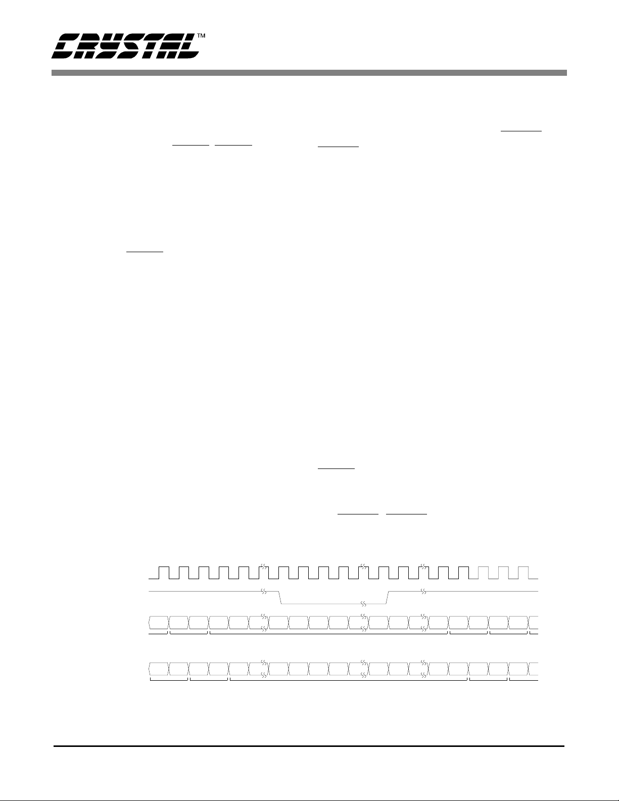
signals. Figure 6 illustrates horizontal timing for
CCIR601 input in Slave Mode. Note that the
CS4952/3 expec ts to receive the first ac tive pixel
data on clock cycle 245 (NTSC) when bit
SYNC_DLY=0 in the CONTROL_2 Register
(Ox02). When SYNC_DLY=1, it expects the first
active pixel data on clock cycle 246 (NTSC).
Master Mode Input Interface
The CS4952/3 defaults to Slave Mode following
RESET
Mode via the MSTR bit in the CONTROL_0 Register (0x00). In Maste r Mode, the CS4952/3 uses
the VSYNC
high but may be switched into Master
, HSYNC and FIELD device pins as
1686168516841683 1716 1 2 3 128 129 244 245 246 247 248
PAL 27MHz Clock Count 1702
HSYNC* (input)
(SYNC_DLY=0)
(SYNC_DLY=1)
14 DS223PP2
1682
CLK
V[7:0]
YCrY Cb Y Cr Y
active pixel
• • •
#720
V[7:0]
YCrY Cb Y Cr
Cb
active pixel
#719
Figure 6. CCIR601 Input Slave Mode Horizontal Timing
170517041703 1728 1 2 3 128 129 264 265 266 267 268
active pixel
#720
1706
• • •
• • •
horizontal blanki ng activ e pixel#1active pixel
horizontal blanking active pixel#1active pixel
• • •
• • •
• • •NTSC 27MHz Clock Count
• • •
#2
#2

CS4952/53
outputs to schedul e the prope r exte rnal deli very o f
digital video int o the V [7:0] pins. Figur e 7 illustrates horizontal timing for CCIR601 input in Master Mode. Note that the CS4952/3 expects to
receive the first active pixel data on clock cycle 245
(NTSC) when bit SYNC_DLY=0 in the
CONTROL_2 Register (0x02). When
SYNC_DLY=1, it expects the first active pixel data
on clock cycle 246 (NT SC).
Vertical Timing
The CS4952/3 can be selected through the
CONTROL_0 register (0x00) to operate in four
different ti ming modes: PAL which is 625 ve rt ic al
lines 25 frames per second interlaced, NTSC which
is 525 vertical lines 30 frames per second interlaced
and both PAL and NTSC a gain but in Progressive
Scan where the display is non-interlaced.
The CS4952/3 conforms to standard digital decompression dimensions and does not process digital
input data for the ac tive analo g video half line s as
they are typically in the over/un derscan regio n of
televisions. For NTSC, 240 active lines total per
field are processed and for PAL 288 active lines total per field. Frame vertical dimensions are 480
lines for NTSC and 576 lines for PAL. Table 1
specifies active li ne numbers for both NTSC and
PAL. Refer to Figure 8 for HSY NC
, VSYNC and
FIELD signal timi ng.
ACTIVE
MODE FIELD
NTSC 1, 3
2, 4
PAL 1, 3, 5, 7
2, 4, 6, 8
LINES
22-261
285-524
23-310
336-623
NTSC Progressive-Scan NA 22-261
PAL Progressive-Scan NA 23-310
Table 1. Vertical Timing
Horizontal Timing
HSYNC is used to synchronize the horizontal input
to output timing in order to provide proper horizontal alignment. HSYNC
lowing RESET
but switches to output in Master
Mode (CONTROL_0 [4] = 1). Horizontal timing is
referenced to HSYNC
video lines, digital video inpu t is to be appli ed to
the V [7:0] inputs 244 (NTSC) or 264 (PAL), CLK
periods following HSYNC
the horizont al alignmen t of the active video.
defaults to an inp ut pin fol-
transitioning low. For active
going low to determine
PAL 27MHz Clock Count
CLK
HSYNC* (output)
CB* (output)
V[7:0]
(SYNC_DLY=0)
V[7:0]
(SYNC_DLY=1)
1682
1702
YCrY Cb Y Cr Y
active pixel
• • •
#720
YCrY Cb Y Cr
Cb
active pixel
#719
170517041703 1728 1 2 3 128 129 264 265 266 267 268
active pixel
#720
1706
• • •
• • •
horizontal blanking active pixel#1active pixel
horizontal bl anking ac t i ve pixel#1act ive pixel
• • •
• • •
• • •NTSC 27MHz Clock Count
• • •
#2
#2
1686168516841683 1716 1 2 3 128 129 244 245 246 247 248
Figure 7. CCIR601 Input Master Mode Horizontal Timing
DS223PP2 15
NTSC Vertical Timing (odd field)
CS4952/53
Line
HSYNC*
VSYNC*
FIELD
Line
HSYNC*
VSYNC*
FIELD
Line
HSYNC*
VSYNC*
3 4 5 6 7 8 9 10
NTSC Vertical Timing (even field)
264 265 266 267 268 269 270 271
PAL Vertical Timing (odd field)
265 1 2 3 4 5 6 7
FIELD
PAL Vertical Timing (even field)
Line
HSYNC*
VSYNC*
FIELD
311 312 313 314 315 316 317 318
Figure 8. Vertical Timing
16 DS223PP2

CS4952/53
NTSC Interlaced
The CS4952/3 supports NTSC-M and PAL-M
modes where the re are 525 to tal lines pe r frame and
two fixed 262.5 line fields per frame and 30 total
frames occuring per secon d. Please reference Figure 9 for NTSC interlaced vertical timing. Each
field consists of 1 l ine for closed ca ption, 240 active lines of video plus 21.5 lines of blanking.
VSYNC
of line 4 and will remain low for 3 lines or (858 x 3)
2574 pixel cycles. The CS4952/3 exclusively reserves line 21 of field one for closed caption insertion. Digital video input is expected to be delivered
to the CS495 2/3 V [7:0] pin s for 240 lines beg inning on active video lines 22 and continuing
field one transistions low at the beginning
Analog
Field 1
VSYNC* Drops
through line 261. VSYNC field two transistions
low in the middle of line 266 and stays low fo r 3
lines times and transitions high in the middle of line
269. The CS4952/3 exclusively reserves line 284 of
field two for closed ca ption insertion. Video input
on the V [7:0] pins is expect ed between lines 285
through line 525.
PAL Interlaced
The CS4952/3 sup ports PAL mode s B, D, G , H, I,
N, and Com bination N wher e there are 625 total
lines per frame and two fixed 312.5 l ine fiel ds per
frame and 25 total frames occuring per second.
Please reference Fi gure 10 for PAL in terlaced vertical timin g. Each fi eld con s ists of 28 8 ac tive li nes
of video plus 24.5 lines of blanking.
523 524 525 1 2 3 4 5 6 7 8 9
Analog
Field 2
261 262 263
Analog
Field 3
523 524 525 1 2 3 4 5 6 7 8 9
Analog
Field 4
261 262 263
Burst b egins wit h positive half-cycle Burst begins w ith negative half-cyc le
Figure 9. NTSC Video Interlaced Timming
VSYNC* Drops
10 22
285284272271270269268267266265264
10 22
285284272271270269268267266265264
DS223PP2 17

CS4952/53
VSYNC* Drops
Analog
Field 1
621 622 623
620 624 625 1 2 3 4 5 6 7 23 24
Analog
Field 2
309 310
308 311 312 313 314 315 316 317 318 319 320 336 337
Analog
Field 3
621 622 623
620 624 625 1 2 3 4 5 6 7 23 24
Analog
Field 4
309 310
308 311 312 313 314 315 316 317 318 319 320 336 337
Analog
Field 5
621 622 623
620 624 625 1 2 3 4 5 6 7 23 24
Analog
Field 6
309 310
308 311 312 313 314 315 316 317 318 319 320 336 337
Analog
Field 7
621 622 623
620 624 625 1 2 3 4 5 6 7 23 24
Analog
Field 8
309 310
308 311 312 313 314 315 316 317 318 319 320 336 337
Burst Phase = 135 degrees relative to U Burst Phase = 225 degrees relative to U
Figure 10. PAL Video Interlaced Timing
18 DS223PP2

CS4952/53
VSYNC will transition low to begin field one and
will remain lo w for 2.5 lines or (864 x 2.5) 2160
pixel cycle s. Digital vi deo input is ex pected to be
delivered to the CS4952/3 V [7:0] pins for 287
lines beginning on active video line 24 and continuing through li ne 310.
Field two begins with VSYNC
after 312.5 lin es from the beginning of f ield one.
VSYNC
tions high with the beginning of line 315. Video input on the V [7:0] pins is expected between line 336
through line 622.
stays low for 2.5 lines times and tra nsi-
transitioning low
Progressive Scan
The CS4952/3 supports a progessive scan mode
where the video output is non-interlaced. This is
accomplished by displaying only the first video
field for NTSC or PAL. To preserve exact MPEG-2
frame rates of 30 a nd 25 per second, th e CS4952/3
displays the sa me first field repet itively but alternately varies the field times. Other digital video encoders commonly support progressive scan by
repetitively displaying a 262 line field (524/525
lines for NTSC). In the long run this method is
flawed in that over time, the output display rate will
overrun a system clock locked MPEG-2 decompressor and display a field twice every 8.75 seconds.
PAL Progressive Scan
VSYNC will transistion low to begin field one and
will remain low for for 2.5 lines or (864 x 2.5) 2160
pixel times. Please reference Figure 11 for PAL
non-interlaced timing. Digital video input is expected to be delivered to the CS4952/3 V [7:0] pins
for 288 lines beginning on active video line 23 and
continuing through line 309.
Field two begins with VSYNC
after 312 lines from the beginning of field one.
transitioning low
VSYNC
high during the m iddle of line 3 15. Video input on
the V [7:0] pins is expected between line 335
through line 6 22. Fi el d two is 313 line s l ong while
field one is 312.
stays low for 2. 5 line ti mes and tr ansiti ons
NTSC Progressive Scan
VSYNC will transition lo w at line 4 to begin fie ld
one and will remain low for 3 lines or (8 58 x 3)
2574 pixel times. Please reference Figure 12 for
NTSC interlaced timing. Digital video input is expected to be delivered to the CS4952/3 V [7:0] pins
for 240 lines beginning on active video line 22 and
continuing through line 261.
Field two begins with VSYNC
line 266. VSYNC
transitions high during the middle of line 268. Video input on the V [7:0] pi ns is expected be tween
line 284 th rough line 524. Field two is 2 63 lines
long while field one is 262.
stays low for 2.5 line times and
transitioning low at
CCIR-656
The CS4952/3 sup ports an additional Sla ve Mode
feature that is selectable throu gh the CCIR601 bit
of the CONTROL_0 register. The CCIR-656 slave
feature is unique because the hori zontal and vertical timing and digital video are combined into a
single 8-bit 27 MHz input. With CCIR-656 there
are no horizontal and vertical input or output
strobes, only 8-bit 27 MHz active CbYCrY data
with start and end of video codes being implemented with reserved 00 and FF code sequ en ces wit hin
the video feed. As with all modes, V [7:0] are sampled with the r ising edge of CLK. The C S4952/3
expects the digital CCIR-656 stream to be error
free. The FIELD output toggles as with non
CCIR-656 input. CCIR-656 input timing is illustrated in Fig ure 13.
DS223PP2 19

VSYNC* Drops
Analog
Field 1
CS4952/53
309 310 311
308 311 312
309 310 311
308 311 312
309
309
Burst Phase = 135 degrees relative to U Burst Phase = 225 degrees relative to U
312 313 1 2 3 4 5 6 7 23 24
310
312 313 1 2 3 4 5 6 7 23 24
310
Figure 11. PAL Video Non-Interlaced Progressive Scan Timing
Analog
Field 2
12345 67 23 24
Analog
Field 3
Analog
Field 4
12345 67 23 24
20 DS223PP2

CS4952/53
262 263
Start of
VSYNC
1 23456 78910 22
Field 1
Field 2
261 262
262 263
1 23456 78910 22
Start of
VSYNC
1 23456 78910 22
Field 3
Field 4
261 262
1 23456 789
10 22
Burst begins with positive half-cycle Burst begins with negative half-cycle
Burst phase = reference phase = 180 relative to B-Y
0
Burst phase = reference phase = 180 relative to B-Y
0
Composite
CCIR656
DATA
Video
V[7:0]
Y
CrYFF 10XY00
Active Video
Figure 12. NTSC Video Non-Interlaced Progressive Scan Timing
00 80 10 80 10 80 10 80 80 10 80 10 80 10 FF XY00 00 CbYCrCbY
EAV Code
4 Clocks
Ancilliary D ata
268 Clocks (NTSC)
280 Clocks (PAL)
Horizontal Blanking
SAV Code
4 Clocks
Active Video
Figure 13. CCIR656 Input Mode Timing
Cr
1440 Clocks
DS223PP2 21

CS4952/53
NTSC-MCCI
NTSC-MC
Address Register
0x00 CONTROL_0 01h 01h 21h 41h 61h A1h 81h
0x01 CONTROL_1 04h 00h 04h 04h 04h 04h 04h
0x10 SC_AMP 1Ch 1Ch 1Ch 15h 15h 15h 15h
0x11 SC_SYNTH0 3Eh 3Eh 3Eh 96h 4Eh 96h 8Ch
0x12 SC_SYNTH1 F8h F8h F8h 15h 4Ah 15h 28h
0x13 SC_SYNTH2 E0h E0h E0h 13h E1h 13h EDh
0x14 SC_SYNTH3 43h 43h 43h 54h 43h 54h 43h
CIR601
Table 2. Multi-standard Format Register Configurations
(Slave Mode, interlaced timing, non-656 data)
R60
(Japan)
NTSC-MR
S170A
PAL-B,D,
G,H,I PAL-M PAL-N
PAL-NCom
(Argentina)
Digital Video Input Modes
The CS4952/3 provides 2 different digital video input modes that are selectable through the
IN_MODE bit of the CONTROL_0 register.
In mode 0 and upon RESET, the CS4952/3 defaults
to output a soli d color (1 of a possib le of 256 col ors). The backgrou nd color is selected by writing
the BKG_COLOR registe r (0x08). Th e colo rspace
of the register is RGB 3:3:2 and is unaffe cted by
gamma correction. The default color following RESET is blue.
In mode 1 the CS4952/3 supports a single 8-bit
27 MHz CbYCrY source as input on the V [7:0]
pins. Input video timing can be CCIR601 master or
slave and progressiv e sca n.
Multi-standard Output Format Modes
The CS4952/53 supports a wide range of output
formats compatible with worldwide broadcast standards. These formats include NTSC-M,
PAL-B/D/G/H/I, PAL-M, PAL-N and P AL Com bination N (PAL-Nc) which is the broadcast standard
used in Argentina. Af ter RESET, the CS495 2/53 defaults to NTSC-M operation with CCIR601 analog
timing. NTSC-M can also be supported in the Japanese format by turning off the 7.5 IRE pedestal
through the PED bit in the CONTROL_1 register
(0x01).
Output format s are configured by writing control
registers as shown in Table 2.
Subcarrier Generation
The CS4952/3 automatically synthesizes NTSC
and PAL color subcarrier clocks using the CLK frequency and four control registers
(SC_SYNTH0/1/2/3). The NTSC subcarrier synthesizer is reset every four fiel ds and every eight
fields for PAL.
The SC_SYNTH0/1/2/3 registers used together
provide a 32-bit value which defaults to NTSC values of 43E0 F 83Eh following rese t.
Table 3 in dicates the 32-bi t valu e required for the
different broadcast forma ts.
Subcarrier Compensation
Since the subcarrier is synthe sized from CLK the
subcarrier freque ncy error wi ll track the clock fre quency error. If the input clock ha s a tolerance o f
200 ppm then the resulting subcarrier will also
have a tolerance of 200 ppm. Per the NTSC speci-
fication the final subcarrier tolerance is ±10 Hz
which is mo re like 3 ppm. Care must be t aken in selecting a suitable cloc k s o urce.
In MPEG-2 system environments the clock is actually recove red from the data stream. In these c ase s
the recovered clock can be 27 MHz ±50 ppm or
22 DS223PP2

System Fsubcarrier Value (dec) Value (hex)
NTSC-M 3.5795455 MHz 1138817086 43E0F83E
PAL-B, D, G, H, I, N 4.43361875 MHz 1410536854 54131596
PAL-N (Argentina) 3.582056 MHz 1139615885 43ED288D
PAL-M 3.579611 MHz 1138838095 43CDDFC7
Table 3. Multi-standard Format FSC Register Configurations
CS4952/53
±1350 Hz. It varies per television but in many cases
given an MPEG-2 system clock of 27 MHz
±1350 Hz the resultant color subcarrier produced
will be outsid e of the tele visio ns abil ity to compe nsate and the ch rominance informati on will not be
displayed (black and white pictu re only).
The CS4952/3 is designed to provide automatic
compensation for an excessively inaccurate
MPEG-2 system clock. Sub-carrier compensation
is enabled through the XTAL bit of the
CONTROL_2 register. When enabled the
CS4952/3 will utilize a common quart z c o lor burst
crystal (3.579545 MHz ±50 ppm for NTSC) attached to the ADDR and XTAL pins to automatically compare and compensate the color subcarrier
synthesis process. Use of the ADDR and XTAL
pins requires that the host interface is configured
2
C operation.
for I
Closed Caption Insertion
The CS4952/3 is capable of NTSC Closed Caption
insertion on lines 21 and 284 independently.
Closed captioning is enabled for either or both lines
21 & 284 via the CC_EN [1:0] register bits and data
to be inserte d is also written int o the four Closed
Caption Data registers. The CS4952/3 when enabled auto matically ge nerates the sev en cycles of
clock run-in (32 x line rate), start bit insertion
(001)and finally insertion of the two data bytes per
line. Data low at the video outputs corresponds to 0
IRE and data high corresponds to 50 IRE.
& CC_284_2 for line 284). Inte rrup ts are also provided to simplify the handshake between the driver
software and the chip. Typically the host would
write all 4 byt es to be inse rted into th e regi sters and
then enable closed caption insertion and interrupts.
As the closed caption interrupts occur the host software would respond by wri ting the next two bytes
to be inserted to the correct control registers and
then clear the interrupt and wait for the next field.
Color Bar Generator
The CS4952/3 is equipped with a color bar generator that is enabled through the CBAR bit of the
CONTROL_1 register. The color bar generator
works in Master or Sla ve Mode and has no e ffect
on the video input/output timing. If the CS4952/3 is
configured for Slave Mode color bars, proper video
timing must be present on the HSYNC
VSYNC
pins for the color bars to be displayed.
Given proper Slave Mode input timing or Master
Mode, the color bar generator will override the video input pixel data.
The output of the color bar generator is instantiated
after the ch roma int erpolat ion filte r and bef ore the
luma delay lin e. The generat ed color bar numbe rs
are for 100% amplitude, 100% saturation NTSC
EIA color bars o r 100% amplitude, 10 0% saturation PAL EBU color ba rs. For PAL col or bars, the
CS4952/3 generates NTSC color bar values, which
are very close to standa rd PAL values. The exact
luma and chroma valu es a r e li s ted in Table 4.
and
There are tw o independent 8-bit re gisters per line
(CC_21_1 & CC_21_ 2 for line 21 and CC _284_1
DS223PP2 23

COLOR Cb Cr Y
White 0 0 +180
Yellow -84 + 14 +162
Cyan +28 -84 +131
Green -56 -70 +112
Magenta +56 +70 +84
Red -28 +84 +69
Blue +84 -14 +35
Black 0 0 +16
Table 4. Internal Color Bar Values
(8-bit values, Cb/Cr are in 2’s complement format)
Interrupts
CS4952/53
GPIO_CTRL_REG [7: 0] bi ts are cleared. In GPIO
input mode, the CS4952/53 will latch the data on
the PDAT [7: 0] p ins into t he corre spondin g b it lo cations of GPIO_DATA_REG when it detects reg-
2
ister address 0x0A through the I
detection of address 0x0A can happen in two ways.
The first a nd mo st co mmon way th is will h appen is
when address 0x0A is written to the CS4952/53 via
2
C interfa ce. T he sec ond m etho d for detect ing
its I
address 0x0A is implemented by accessing register
2
address 0x09 through I
C. In I2C host interface operation, the CS4952/53 register address pointer will
auto-increment to address 0x0A after an address
0x09 access.
C interface. A
In order to better support precise video mode
switches and to establish a software/hardware
handshake w ith the cl osed caption insertion block
the CS4952/3 is equipped with an interrupt pin
named INT. The INT pin is ac tive hi gh. The re are
three interrupt sources: VSYNC
, Line 21 a nd Line
284. Each interrupt can be individually disabled
with the INT_EN register. Each interrupt is also
cleared via writing a one to the corresponding
INT_CLR regist er bits. Th e thre e individua l inter rupts are ORed together to generate an interrupt
signal which i s pre sented on the INT output p in. If
an interrup t has occurred, i t cannot be elim inated
with a disable, i t m ust be cleared.
General Purpose I/O Port
The CS4952/53 has a GPIO port and register which
2
is availabl e when the device is configure d for I
2
host interface operation. In I
C host interface
mode, the PDAT [7:0] pins are unused by the host
interface and they may operate independently as input or output p in s for the GPIO_DATA_REG register (0x0A). The CS4952/53 also contains the
GPIO_CTRL_REG Re gister (0x09) whic h is used
to configure the GPIO pins for input or ou tput operation.
C
The GPIO port PDAT [7:0] pins are configured for
output operation when the corresponding
GPIO_CTRL_REG [7:0] bits are set. In GPIO output mode, the CS4952/53 will output the data in
GPIO_DATA_REG [7:0] bit locations onto the
corresponding PDAT [7:0] pi ns when it detects a
2
register address 0x0A through the I
C interface.
ANALOG
Analog Timing
All CS4952/3 analog timing and sequencing is derived from the 2 7 MHz clock inp ut. Th e an alog outputs are controlled internally by the video timing
generator in conjunction with master and slave timing. The video output signals perform accordingly
for NTSC, PAL specifications and both modes again
but with progressive scan non-interlaced video output.
Being that the CS4952/3 is almost entirely a digital
circuit, great care has been taken to gu arantee analog timing a nd slew rat e performa nce as spec ified
in the NTSC and PAL analog specifications. Reference the Analog Parameters section of this data
sheet for exact pe rformance param et ers.
The GPIO port PDAT [7:0] pins are configured for
input operation when the corresponding
24 DS223PP2

CS4952/53
VREF
The CS4952/ 3 can ope rate wi th or with out the a id
of an ext ernal volt age refe rence. T he CS495 2/3 is
designed with an internal voltage reference generator that provides a VREFOUT signal. The internal
voltage reference is utilized by electrically connecting the VREFOUT and VREFIN pins. VREFIN can also be connected to an external precision
1.235 v olt reference . In eith er case, VR EFIN is to
be decoupled to ground with a 0.1 µF capacitor.
Decoupling should be applied as close to the device
pin as possible.
ISET
All four of the CS4952/3 digital to analog converter
DACs are output curre nt normalized with a com mon ISET device pin. The DAC output current per
bit is determined by the size of the resistor connected between ISET and electrical ground. Typically a
10 kΩ±1% m et al fi lm resistor should be u sed. T he
ISET resistance can be change d by the user to accommodate varying video output attenuation via
post filters and also to suit individual preferred performance.
In conjuncti on with the ISET value , the user may
also independe ntly vary the ch rom a, luma and col orburst amplit ude levels v ia host addressa ble control register bits that are used to control internal
digital amplif iers. The DAC output levels are defined by the fol lowing operat ions:
VREFIN/RISET = IREF
1.235 V/10 kΩ = 123.5 µA
CVBS37/Y/C Outputs:
VOUT (max) = IREF × (8/15) ×511 × 37.5 Ω =
1.262 V
CVBS75 Output:
VOUT (max) = IREF × (4/15) ×511 × 75 Ω =
1.262 V
DACs
The CS4952/3 is equipped with 4 independent video grade current output digital to analog converters.
They are 9-b it DACs operatin g at a 27 MHz two
times oversampling rate. All four DACs are disabled and put in a l ow power mode upo n RESET.
All four DACs can be indi viduall y powered down
and disabled. The output c urren t p er bi t of al l fou r
DACs is determined by the size of resistor connected between the ISE T pin and electrica l ground.
Luminance DAC
The Y pin is drive n from a 9-bit 27 MHz current
output DAC that internally receives the Y or luminance portion of t he video sig nal (black an d white
intensity and syn cronization informat ion only). Y
is designed to drive proper video levels into a
37.5 Ω load. Ref erence the deta iled elect rical section of this data sheet for the exact Y digital to analog AC and DC performance data. A Y_EN
enable control bit in the DAC register (0x08) is
provided t o ena bl e or d isabl e th e l umi nan ce D AC.
For a complete disa ble and lowe r power op eration
the Lum inance DAC c an be tot ally shut down via
the Y_PD control bit in the DAC register (0x08). In
this mode t urn-on thro ugh the cont rol regist er wi ll
not be instantaneous.
Chrominance DAC
The C pin is driven from a 9 -bit 27 MHz current
output DAC that internally receives the C or
chrominance portion of the video signal (color
only). C is designed to drive proper video levels
into a 37.5 Ω load. Reference the detailed electrical
section of this data sheet for the exact C digital to
analog AC and DC performance data. A C_EN enable con trol re gister b it in the DAC register (0x08)
is provided to ena ble or disable the Chrom inance
DAC. For a complete disable and lower power operation t he Chromin ance DAC can be tota lly shut
down via the C_PD c on trol register bit in the DAC
DS223PP2 25

CS4952/53
register (0x08). In this mode turn-on through the
control regi ste r will not be instantaneous.
CVBS75 DAC
The CVBS75 pin is driven from a 9-bit 27 MHz
current ou tput DAC that internally receives a combined luma and chroma sign al to provi de compo site video output. CVBS75 is designed to drive
proper composite video levels into a 75 Ω load.
Refere nce the det ailed el ectrical s ection o f this data
sheet for the exa ct CVBS75 digital to anal og AC
and DC performance data. A C_75_EN enable control register bit in the DAC r egister (0x 08) is provided to enable or disable the ouput pin. When
disabled, no cur rent flows from the output. For a
complete disable and lower power operation the
CVBS75 DAC can be totally shut down via the
C_75_PD cont rol register bit in the DAC register
(0x08). In this mode turn-on through the control
register will not be instantaneous.
CVBS37 DAC
The CVBS37 pin is driven from a 9-bit 27 MHz
current output DAC that internally receives a combined luma and chroma sig nal to provi de compo site video output. CVBS37 is designed to drive
proper compo site video levels in to a 37.5 Ω load.
Reference the detailed electrical section of this data
sheet for the exa ct CVBS37 digital to anal og AC
and DC performance data. The C_37_EN DAC enable control register bit is in the DAC register
(0x08) provided to enable or di sabl e the ouput pin.
When disabled, no current flow from the output.
For a complete disa ble and lowe r power op eration
the CVBS37 DAC can be totally shut down via the
C_37_PD control register bit in the DAC register
(0x08). In this mode turn-on through the control
register will not be instantaneous.
26 DS223PP2

PROGRAMMING
Host Control Interface
The CS4952/3 host control interface can be config-
2
ured for I
CS4952/3 will default to I
and WR pins are both tied low at power up. The
RD
and WR pins are active fo r 8-b it par alle l oper -
RD
C or 8-bit parallel operation. The
2
C operation when the
ation only.
I2C Interface
The CS4952/3 provides an I2C interface for accessing the internal control and status registers. External
pins are a bidirectional data pin (SDA) and a serial
2
input clock (SCL). The protocol follows the I
specifications. A complete data transfer is shown in
2
Figure 14. Note that this I
C interface will work in
Slave Mode only - it is not a bus master.
SDA and SCL are connected via an external
pull-up resistor to a positive supply volta ge . W hen
the bus is free, both lines are high. The output stages of devices connected to the bus must have an
open-drain or open-collector in order to perform
2
the wired-AND fun ction. Dat a on the I
C bus can
be transferred at a rate of up to 400 kbits/sec in fast
mode. The number of interfaces to the bus is solely
dependent on the limiting bus capacitance of
400 pF . When 8-bi t parallel in terface oper ation is
being used, SDA and SCL can be tied directly to
ground.
C
CS4952/53
2
The I
mable via register I2C_ADR (0x0F).
8-bit Parallel Interface
The CS4952/3 is equipped with a full 8-bit parallel
microprocessor write and read con trol p ort. Along
with the PDAT [7:0] pins the control port interface
is comprised of host rea d RD
active low strobes and host ad dress enable ADDR
which, when low, enables unique address register
accesses. The control port is used to access internal
registers which configure the CS4952/3 for various
modes of operation. The internal registers are
uniquely addressed via an address register. The address register is acce ssed dur in g a host wri te c ycle
with the W R
cycles with ADDR set high will write the 8-bits on
the PDA T [7:0 ] pins in to the regist er cur rentl y selected by the address register. Likewise read cycles
occur with RD
turn the register contents selected by the address
register. Reference the detailed electrical timing
parameter se ction of this da ta sheet for exact host
parallel in terface timi ng charac teristics an d specifications. When I
used, RD
PDAT [7:0] are available to be used for GPIO op eration in I
C bus address for t he CS49 52/3 is progra m-
and host write WR
and ADDR pins set low. Host write
set low and ADDR set high will re-
2
C interface operation is being
and WR must be tied to ground.
2
C host interfa ce mode.
2
I C Protocol
SDA
SCL
A P
Start Address
DS223PP2 27
1-7
Note: I C transfers data always with MSB first, LSB last
89
R/W
2
1-7
ACK Data Stop
Figure 14. I2C Data Transfer
89
ACK
1-7
89
Data ACK

CS4952/53
Register Description
A set of inte rnal registe rs are availa ble for controlling the oper ation of the CS4952/3. The registers
extend from int ernal address 0x00 through 0x 3D.
Table 5 shows a complete list of these registers and
Address Register Name Type Default Value
0x00 CON TROL_0 r/w 01h
0x01 CON TROL_1 r/w 04h
0x02 CON TROL_2 r/w 00h
0x03 RESERVED
0x04 DAC r/w F0h
0x05 - 0x06 RESERVED
0x07 STATUS read only 00h
0x08 BKG_CO LOR r/w 03h
0x09 GPIO_CTRL_REG r/w
0x0A GPIO_DATA_REG r/w 00h
0x0B - 0x0C RESERVED
0x0D C_AMP r/w 80h
0x0E Y_AMP r/w 80h
0x0F I2C_ADR r/w n/a
0x10 SC_AMP r/w 1Ch
0x11 SC_SYNTH0 r/w 3Eh
0x12 SC_SYNTH1 r/w F8h
0x13 SC_SYNTH2 r/w E0h
0x14 SC_SYNTH3 r/w 43h
0x15 HUE_LSB r/w 00h
0x16 HUE_M SB r/w 00h
0x17 RESERVED
0x18 CC_EN r/w 00h
0x19 CC_21_1 r/w 00h
0x1A CC_21_2 r/w 00h
0x1B CC_284_1 r/w 00h
0x1C CC_284_2 r/w 00h
0x1D - 0x3A RESERVED
0x3B INT_EN r/w 00h
0x3C INT_CLR r/w 00h
0x3D ID_REG read only n/a
their internal addresses. Note that this table and the
subsequent register description section describe the
full register map for CS4952 only. A complete
CS4953 register set description is only available to
Macrovision ACP-PPV Licensed Buyers.
Table 5. Control Register Map
28 DS223PP2

CS4952/53
Control Registe r 0
Address 0x00 CONTROL_0 Read/Write Default Value = 01h
Bit Number76543210
Bit Name TV_FMT MSTR CCIR656 PROG IN_MODE CBCR_UV
Default00000001
Bit Mnemonic Function
7:5 TV_FMT selects the TV display format
000: NTSC-M CCIR601 timing (default)
001: NTSC-M RS170A timing
010: PAL-B, D, G, H, I
01 1: PAL-M
100: PAL-N (Argentina)
101: PAL-N (non Argentina)
110-111: reserved
4 MSTR 1: Master Mode, 0: Slave Mode
3 CCIR656 video input is in CCIR656 format (0: off, 1: on)
2 PROG Progressive scanning enable (enable with 1)
1 IN_MODE Input select (0: solid background, 1: use V [7:0] data)
0 CBCR_UV enable YCbCr to YUV conversion (1: enable, 0: disable)
Control Registe r 1
Address 0x01 CONTROL_1 Read/Write Default Value = 04h
Bit Number76543210
Bit Name CBLANK Y_DELAY C_BW C_LPF_EN FLD PED CBAR CBC RSEL
Default00000100
Bit Mnemonic Function
7 CBLANK Composite Blank / HSYNC output select (1: CB, 0: HSYNC)
6 Y_DELAY luma to chroma delay (0: no delay, 1: luma is delayed by one 13.5 MHz cycle)
5 C_BW chroma lpf bandwidth (0: 650 KHz, 1: 1.3 MHz )
4 C_LPF_EN chroma lpf on/off (0: off, 1: on)
3 FLD Pol arity of Field (0: odd field - 0, 1: odd field - 1)
2 PED Pedestal offset (0: 0 IRE, 1: 7.5 IRE)
1 CBAR internal color bar generator (0: off, 1: on)
0 CBCRSEL CbCr select (0: chroma undelayed, 1: chroma delayed by one clock)
DS223PP2 29

CS4952/53
Control Registe r 2
Address 0x02 CONTROL_2 Read/Write Default Value = 00h
Bit Number76543210
Bit Name RESERVED SYNC_DLY XTAL SC_EN
Default00000000
Bit Mnemonic Function
7:4 - reserved
Selects between 4.2 Mhz and 6 Mhz on-chip luminance low pass filters; default
3Y_BW
2 SYNC_DLY
1 XTAL Crystal oscillator for subcarrier adjustment enable (1: enable)
0 SC_EN Chroma burst disable (1: disable)
DAC Power Down Register
value is zero which selects the 4.2 Mhz low pass filter option
Delays expected timing of first active pixel input data relative to falling edge of
HSYNC from 245 27 MHz clock cycles to 246 for NTSC and from 265 to 266 for
PAL. Default State is SYNC_DL Y=0 for no delay
Address 0x04 DAC Read/Write Default Value = F0h
Bit Number76543210
Bit Name C_75_PD C_37_PD Y_PD C_PD C_75_EN C_37_EN Y_EN C_EN
Default11110000
Bit Mnemonic Function
7 C_75_PD power down composite DAC with 75 Ω load (0: power up, 1: power down)
6 C_37_PD power down composite DAC with 37.5 Ω load (0: power up, 1: power down)
5 Y_PD power down luma s-video DAC (0: power up, 1: power down)
4 C_PD power down chroma s-video DAC (0: power up, 1: power down)
3 C_75_EN enable composite video DAC output for 75 Ω (0: tri-state, 1: enable)
2 C_37_EN enable composite video DAC output for 37.5 Ω (0: tri-state, 1: enable)
1 Y_EN enable s-video DAC for luma output (0: tri-state, 1: enable)
0 C_EN enable s-video DAC for chroma output (0: tri-state, 1: enable)
30 DS223PP2

CS4952/53
Status Register
Address 0x07 STATUS Read Only Default Value = 00h
Bit Number76 5 4 3 210
Bit Name RESERVED CC_INT_21 CC_INT_284 VS_INT FIELD
Default 0 0 0 0 0 0 0 0
Bit Mnemonic Function
7:6 - reserved
5 CC_INT_21 Interrupt flag for line 21 (closed caption) complete
4 CC_INT_284 Interrupt flag for line 284 (closed caption) complete
3 VS_INT Interrupt flag for video field change
2:0 FIELD Field Status bits
000: field 8
001: field 1
010: field 2
011: field 3
100: field 4
101: field 5
110: field 6
111 : fie ld 7
Background Co lor Register
Address 0x08 BKG_ COL OR Read/Write De fa ul t Value = 03h
Bit Number76543210
Bit Name BG_COLR
Default00000011
Bit Mnemonic Function
7:0 BG_COLR Background color (7:5 = R, 4:2 = G, 1:0 = B)
GPIO Control Register
Address 0x09 GPIO_C TRL_REG Re ad/Write Default Value = 00h
Bit Number76543210
Bit Name GPIO_IO
Default00000000
Bit Mnemonic Function
7:0 GPIO_IO input(0)/output(1) control of GPIO registers (bit X: PDAT(X) I/O configuration)
DS223PP2 31
CS4952/53
GPIO Data Register
Address 0x0A GPIO_DATA_REG Read/Write Default Value = 00h
Bit Number76543210
Bit Name GPIO _ D ATA
Default00000000
Bit Mnemonic Function
7:0 GPIO_DATA
Chroma Filter Register
Address 0x0D C_AMP Read/Write Default Va lue = 80h
Bit Number76543210
Bit Name C_COEF
Default10000000
GPIO data register; data is output on PDAT [7:0] bus if appropriate bit in
GPIO_CTRL_REG (0x09) is set to “1”; data on PDAT [7:0] is latched into
GPIO_DATA_REG [7:0] when register address 0x0A is accessed via I
2
This register is only accessible in I
C mode.
2
C.
Bit Mnemonic Function
7:0 C_COEF Chroma amplitude coefficient
Luma Filter Register
Address 0x0E Y_AMP Read/Write Defaul t Va lue = 80h
Bit Number76543210
Bit Name Y_COEF
Default10000000
Bit Mnemonic Function
7:0 Y_COEF Luma amplitude coefficient
2
C Address Register
I
Address 0x0F I2C_ADR Read /Write Defaul t Va lue = N/A
Bit Number7 6543210
Bit Name RESERVED ADDR
Default - -------
Bit Mnemonic Function
7 - reserved
6:0 ADDR I
32 DS223PP2
2
C device address (programmable)

CS4952/53
Subcarrier Ampl itude Register
Address 0x10 SC_AMP Read/Wri te De fa ul t Value = 1Ch
Bit Number76543210
Bit Name AMP
Default00011100
Bit Mnemonic Function
7:0 AMP Color burst amplitude
Subcarrier Synthe sis Register
Address 0x11 SC_SYNTH0 Read/Write Default Value = 3Eh
0x12 SC_SYNTH1 F8h
0x13 SC_SYNTH2 E0h
0x14 SC_SYNTH3 43h
Register Bits Mnemonic Function
SC_SYNTH0 7:0 - Subcarrier synthesis bits 7:0
SC_SYNTH1 7:0 - Subcarrier synthesis bits 15:8
SC_SYNTH2 7:0 - Subcarrier synthesis bits 23:16
SC_SYNTH3 7:0 - Subcarrier synthesis bits 31:24
Hue LSB Adjust Register
Address 0x15 HUE _L SB Read/Write Default Value = 00h
Bit Number76543210
Bit Name LSB
Default00000000
Bit Mnemonic Function
7:0 LSB 8 LSBs for hue phase shift
Hue MSB Ad jus t Register
Address 0x16 HUE _MSB Read/Write Default Va lue = 00h
Bit Number76543210
Bit Name RESERVED MSB
Default00000000
Bit Mnemonic Function
7:2 - reserved
1:0 MSB 2 MSBs for hue phase shift
DS223PP2 33

CS4952/53
Closed Caption Enable Register
Address 0x18 CC_EN Read/Write Default Value = 00h
Bit Number76543210
Bit Name RESERVED EN_284 EN_21
Default00000000
Bit Mnemonic Function
7:2 - reserved
1 EN_284 enable closed caption for line 284
0 EN_21 enable closed caption for line 21
Closed Caption Data R egi ste r
Address 0x19 CC_21_1 Read/Write Default Va lue = 00h
0x1A CC_21_2 00h
0x1B CC_284_1 00h
0x1C CC_284_2 00h
Register Bit Mnemonic Function
CC_21_1 7:0 - first closed caption databyte of line 21
CC_21_2 7:0 - second closed caption databyte of line 21
CC_284_1 7:0 - first closed caption databyte of line 284
CC_284_2 7:0 - second closed caption databyte of line 284
Interrupt Enable Re gi ster
Address 0x3B INT_E N Read/Write Default Value = 00h
Bit Number76543210
Bit Name RESERVED EN_21 EN_284 VS_EN
Default00000000
Bit Mnemonic Function
7:3 - reserved
2 EN_21 interrupt enable for closed caption line 21
1 EN_284 interrupt enable for closed caption line 284
0 VS_EN i nterrupt enable for new field
34 DS223PP2

CS4952/53
Interrupt Clear Register
Address 0x3C INT_CL R Read/Write Default Value = 00h
Bit Number76543210
Bit Name RESERVED CLR_21 CLR_284 VS_CLR
Default00000000
Bit Mnemonic Function
7:3 - reserved
2 CLR_21 clear interrupt for closed caption line 21 (INT_21)
1 CLR_284 clear interrupt for closed caption line 284 (INT_284)
0 VS_CLR clear interrupt for new video field (INT_V)
Device ID Reg ister
Address 0x3D ID_REG Read Only Default Value = N/A
Bit Number76543210
Bit Name DEV_ID RESERVED
Default 0 0 0 0 - - - -
Bit Mnemonic Function
7:4 DEV_ID 0000 device ID for CS4952
0001 device ID for CS4953
3:0 - These bits are reserved and the value they return on a read is not defined
DS223PP2 35

CS4952/53
BOARD DESIGN & LAYOUT
CONSIDERATIONS
The printed circuit layou t should be opt imized fo r
lowest noise o n the CS4952/3 power and ground
lines. Digital and anal og sections should be physically separated and the CS4952/3 placed as close to
the output conne ctors as possible. All anal og supply traces sh ould be as short as po ssible to minimize inducti ve ringing.
A well designed power di stribution netwo rk is essential in eliminating digital switching noise. The
ground planes must provide a low-imp edance return path for the digital circuits. A PC board with a
minimum of four layers is recommended. The
ground layer should be used as a shield to isolate
noise from the analog traces. The top layer (1)
should be reserved for analog traces but digital
traces may share this layer if the digital signals
have low edge ra tes and switch little current or if
they are sepa rate d fr om th e anal og tra ces by a sig nificant distance (dependent on their frequency
content an d current). The se cond layer should then
be the grou nd pla ne fol lowed by th e ana log p ower
plane on layer th ree and the digital sign al layer on
layer four
Power and Ground Planes
same supply. If necessary, further isolate the digital
and analog power supplies by using ferrite beads on
each supply branc h foll owed by a low ESR c apac itor.
Place all d ecoup ling ca ps as cl ose as possib le to th e
device as possi ble. Surface mou nt capacitors g enerally have lower inductance than radial lead or axial lead components. Surface mount caps should be
placed on the com pone nt si de o f t he PC B to m ini mize inductance caused by board vias. Any vias,
especially to ground, should be as large as practical
to reduce their inductive effects.
VREF Decoupling
The VREFOUT pin provides a 1.235 V reference
for the internal DACs. VREFOUT is only intended
to drive VREF IN. Do not connect to an external
load. A sma ll bypass cap, howe ver, may be pl aced
on VREFOUT to reduce noise. Usually a 0.1uF
MLC surface moun t ca pacitor is sufficie n t.
Digital Interconnect
The digital inputs and outputs of the CS4952/3
should be isolated from the analog outputs as much
as possible. Use separate signal layers whenever
possible and do not route digital sign als over the
analog power and ground planes.
The power and ground planes need isolation gaps
of at 0.05” to minimiz e digital switching noi se effects on the analog signals and components. A split
analog/digital ground plane should be connected at
one point as close as p ossible to the CS4952/ 3. A
split analog/digital power plane should be connected at one point as close as possible to the power entry point and decoupled properly.
Power Supply Decoupling
Start by reduc ing power supply r ipple and wiring
harness inductance by placing a large (33 - 100uF)
capacitor a s close t o the power en try poi nt as po ssible. Use separate power pl anes or traces for the
digital and analog sections even if they use the
36 DS223PP2
Noise from the digital section is directly related to
the digital edge rates used. Ringing, overshoot, undershoot, and ground bounce are all related to edge
rate. Use lower speed logic such as HCMOS for the
host port inter face to reduce swit ching noise. For
the video input ports, higher speed logic is required, but use the slowest practical edge rate to reduce nois e.
To reduce digital noise, it is important to match the
source impedance, line impedance, and load impedance as much as possible. Generall y, if the line
length is greater than one fourth the signal edge
rate, line termination is necessary. Ringing may
also be reduce d by damping t he line with a se ries
resistor (22 - 150 Ω). Under extrem e cases, it may

CS4952/53
be advisable to use microstrip techniques to further
reduce radiated switching noise if very fast edge
rates (<2ns) are used. If microstrip techniques are
used, split the analog and digital ground planes and
use proper RF decoupl ing techniques.
Analog Interconnect
The CS4952/3 shoul d be located as close as p ossible
to the output connectors to minimize noise pickup
and reflections due to impedance mismatch. All unused analog outputs should be placed in shutdown.
This reduces the total power that the CS4952/3 requires, and eliminates the impedance mismatch presented by an unused connector. The analog outputs
should not overlay the analog power plane to maximize high frequency p ower supply rejection.
Analog Output Protection
To minimize the possibility of damage to the analog out p ut sect ions, m ake sur e th at al l video con nectors are we ll grounded. The conne ctor ground
should have a good DC ground pat h to the ana log
and digital powe r supply grounds. If no DC (and
low frequency) path is present, improperly grounded equipm ent may impose dam aging reverse currents on the vid eo out line s. Therefo re, it is also a
good idea to use output filters that a re AC coupl ed
to avoid any problems.
ESD Protection
External DAC Output Filter
If an output filter is required for the composite
and/or S-video outputs of the CS4952/53, the following low pass filter in Figure 15 can be used.
IN
2.2µH
OUT
C
1
330pF 220pF
should be chosen so that =
C
2
Figure 15. Low Pass Filter
C
2
C
CABLE
C
+
C
C
1
CABLE
2
DS223PP2 37

DEVICE PINOUT - 44 PLCC
VAA
CS4952/53
GND
VAA
CVBS37
CVBS75
TEST
V0
V1
V2
V3
V4
V5
V6
V7
FIELD
HSYNC/CB
VSYNC
7
8
9
10
11
12
13
14
15
16
17 29
18 20 22 24 26 28
1246404244
CS4952/3-CL
44-pin
PLCC
Top View
39
38
37
36
35
34
33
32
31
30
C
Y
VREFOUT
VREFIN
ISET
VAA
GND
RESET
SCL
SDA
INT
CLKIN
WR
RD
PDAT0
PDAT1
XTAL
ADDR
VAA
GND
GND
PDAT2
PDAT3
PDAT4
PDAT5
PDAT6
PDAT7
38 DS223PP2

CS4952/53
PLCC Pin Description
Pin Name Pin Number Type Description
V [7:0] 14, 13, 12, 11, 10, 9, 8, 7 IN Digital video data inputs
CLK 33 IN 27 MHz input clock
ADDR 19 IN Address enable line / subcarrier crystal input
XTAL 18 OUT subcarrier crystal output
HSYNC
VSYNC
FIELD 15 OUT Video field ID. Selectable polarity
RD
WR
PDAT [7:0] 23,24,25,26,27,28,29,30 I/O Host parallel port/ general purpose I/O
SDA 35 I /O I
SCL 36 IN I
CVBS75 5 CURRENT Composite video output for driving 75 Ω loads
CVBS37 4 CURRENT Composite video output for driving 37.5 Ω loads
Y 43 CURRENT Luminance analog output for driving 37.5 Ω loads
C 44 CURRENT Chrominance analog output for driving 37.5 Ω loads
VREFOUT 42 OUT Internal voltage reference output
VREFIN 41 IN External voltage reference input
ISET 40 OUT DAC current set
INT 34 OUT Interrupt output, active high
RESET
TEST 6 IN TEST pin. Ground for normal operation
VAA 1, 3, 20, 39 PS +5 V supply
GND 2, 22, 21, 38 PS Ground
/CB 16 I/O Active low horizontal sync, or compos it e blank signal
17 I/O Active low vertical sync.
31 IN Host parallel port read st robe, active low
32 IN Host parallel port write strobe, active low
2
C data
2
C clock input
37 IN Active low master reset
DS223PP2 39
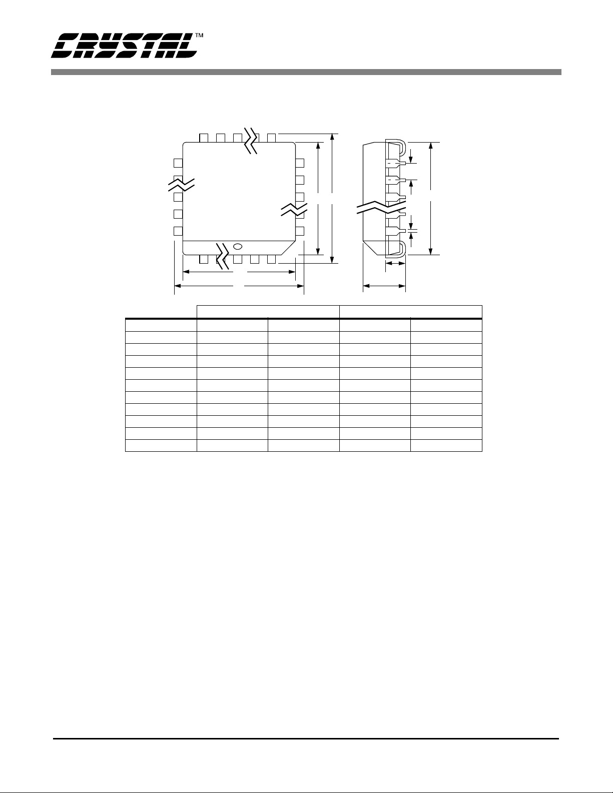
44L PLCC PACKAGE DRAWING
CS4952/53
e
D2/E2
B
D1
D
E1 E
A1
A
INCHES MILLIMETERS
DIM MIN MAX MIN MAX
A 0.165 0.180 4.043 4.572
A1 0.090 0.120 2.205 3.048
B 0.013 0.021 0.319 0.533
D 0.685 0.695 16.783 17.653
D1 0.650 0.656 15.925 16.662
D2 0.590 0.630 14.455 16.002
E 0.685 0.695 16.783 17.653
E1 0.650 0.656 15.925 16.662
E2 0.590 0.630 14.455 16.002
e 0.040 0.060 0.980 1.524
JEDEC # : MS-018
40 DS223PP2

DEVICE PINOUT - 44 TQFP
VAA
CS4952/53
GND
VAA
CVBS 37
CVBS 75
TEST
V0
V1
V2
V3
V4
V5
V6
V7
FIELD
HSYNC/CB
VSYNC
XTAL
C
Y
VREFOUT
VREFIN
ISET
VAA
404244 343638
1
2
3
4
5
6
7
8
9
10
11
CS4952/3-CL
44-pin
TQFP
Top View
12
14 16 18 20 22
33
32
31
30
29
28
27
26
25
24
23
GND
RESET
SCL
SDA
INT
CLKIN
WR
RD
PDA T0
PDA T1
PDA T2
ADDR
VAA
GND
GND
PDA T3
PDA T4
PDA T5
PDA T6
PDA T7
DS223PP2 41

CS4952/53
TQFP Pin Description
Pin Name Pin Number Type Description
V [7:0] 8, 7, 6, 5, 4, 3, 2, 1 IN Digital video data inputs
CLKIN 27 IN 27 MHz input clock
ADDR 13 IN Address enable line / subcarrier crystal input
XTAL 12 OUT subcarrier crystal output
HSYNC
VSYNC
FIELD 9 OUT Video field ID. Selectable polarity
RD
WR
PDAT [7:0] 17,18,19,20,21,22,23,24 I/O Host parallel port/ general purpose I/O
SDA 29 I /O I
SCL 30 IN I
CVBS75 43 CURRENT Composite video output for driving 75 Ω loads
CVBS37 42 CURRENT Composite video output for driving 37.5 Ω loads
Y 37 CURRENT Luminance analog output for driving 37.5 Ω loads
C 38 CURRENT Chrominance analog output for driving 37.5 Ω loads
VREFOUT 36 OUT Internal voltage reference output
VREFIN 35 IN External voltage reference input
ISET 34 OUT DAC current set
INT 28 OUT Interrupt output, active high
RESET
TEST 44 IN TEST pin. Ground for normal operation
VAA 14, 33, 39, 41 PS +5 V supply
GND 15, 16, 32, 40 PS Ground
/CB 10 I/O Active low horizontal sync, or compos it e blank signal
11 I/O Active low vertical sync.
25 IN Host parallel port read st robe, active low
26 IN Host parallel port write strobe, active low
2
C data
2
C clock input
31 IN Active low master reset
42 DS223PP2

44L TQFP PACKAGE DRAWING
CS4952/53
∝
L
1
E1 E
D1
A
D
e
B
A1
INCHES MILLIMETERS
DIM MIN MAX MIN MAX
A 0.000 0.065 0.000 1.600
A1 0.002 0.006 0.050 0.150
B 0.012 0.018 0.300 0.450
D 0.478 0.502 11.700 12.300
D1 0.404 0.412 9.900 10.100
E 0.478 0.502 11.700 12.300
E1 0.404 0.412 9.900 10.100
e 0.029 0.037 0.700 0.900
L 0.018 0.030 0.450 0.750
∝
0.000 7.000 0.000 7.000
JEDEC # : MS-026
DS223PP2 43

 Loading...