CS4392
24-Bit, 192 kHz Stereo DAC with Volume Control
Features
Complete Stereo DAC System: Interpolation,
D/A, Output Analog Filtering
114 dB Dynamic Range
100 dB THD+N
Up to 192kHz Sample Rates
Direct Stream Digital Mode
Low Clock Jitter Sensitivity
Single +5 V Power Supply
Selectable Digital Filters
– Fast and Slow roll-off
Volume Control with Soft Ramp
–1dBStepSize
– Zero Crossing Click-Free Transitions
Direct Interface with 5 V to 1.8 V Logic
ATAPI mixing functions
Pin compatible with the CS4391
I
Description
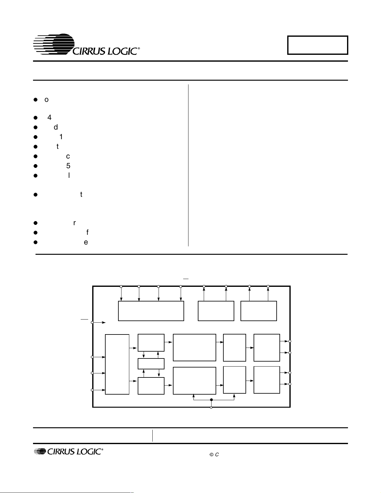
The CS4392 is a complete stereo digital-to-analog system including digital interpolation, fifth-order delta-sigma
digital-to-analog conversion, digital de-emphasis, volume control, channel mixing and analog filtering. The
advantages of this architecture include: ideal differential
linearity, no distortion mechanisms due to resistor
matching errors, no linearity drift over time and temperature, and a high tolerance to clock jitter.
The CS4392 accepts PCM data at sample rates from
4 kHz to 192 kHz, DSD audio data, has selectable digital
filters, and consumes very little power. These features
are ideal for DVD, SACD players, A/V receivers, CD and
set-top box systems. The CS4392 is pin and register
compatible with the CS4391, making easy performance
upgrades possible.
ORDERING INFORMATION
CS4392-KS -10 to 70 °C 20-pin SOIC
CS4392-KZ -10 to 70 °C 20-pinTSSOP
CDB4392 Evaluation Board
M1
M3
MODE SELECT
(CONTROL PO RT)
RST
SCLK
LRCK
SDATA
(SDA/CDIN)
SERIAL
PORT
Preliminary Product Information
http://www.cirrus.com
M2
(SCL/CCLK) ( AD0/CS)
VOLUM E
CONTROL
MIXER
VOLUM E
CONTROL
M0
AMUTEC
MUTE CONTROL
INTERPOLATION
FILTER
INTERPOLATION
FILTER
EXTERNAL
MCLK
∆Σ
DAC
∆Σ
DAC
CMOUT
REFERENCE
FILT+BMUTEC
ANALOG
FILTER
ANALOG
FILTER
This document contains information for a new product.
Cirrus Logic reserves the right to modify this product without notice.
CopyrightCirrus Logic, Inc. 2002
(All Rights Reserved)
AOUTA+
AOUTA-
AOUTB+
AOUTB-
SEP ‘02
DS459PP2
1
TABLE OF CONTENTS
1. PIN DESCRIPTION - PCM DATA MODE .................................................................... 5
1.1 PIN DESCRIPTION - DSD mode ..................................................................... 6
2. TYPICAL CONNECTION DIAGRAMS ........................................................................ 7
3. APPLICATIONS ........................................................................................................... 9
3.1 Recommended Power-up Sequence for Hardware Mode ................................ 9
3.2 Recommended Power-up Sequence and Access to
Control Port Mode ............................................................................................. 9
3.3 Analog Output and Filtering .............................................................................. 9
3.4 Interpolation Filter ........................................................................................... 10
3.5 System Clocking ............................................................................................. 10
3.6 Digital Interface Format .................................................................................. 11
3.7 De-Emphasis .................................................................................................. 12
3.8 Oversampling Modes ...................................................................................... 12
3.9 Using DSD mode ............................................................................................ 13
3.10 Mute Control ................................................................................................. 13
4. CONTROL PORT INTERFACE ................................................................................. 14
4.0.1 MAP Auto Increment ............................................................................. 14
4.0.2 I2C Mode ............................................................................................... 14
4.0.3 SPI Mode ............................................................................................... 16
4.1 Memory Address Pointer (MAP)...................................................................... 16
5. REGISTER QUICK REFERENCE ............................................................................. 17
6. REGISTER DESCRIPTION ........................................................................................ 18
6.1 Mode Control 1 - Address 01h ........................................................................ 18
6.1.1 Auto-Mute (Bit 7) ................................................................................... 18
6.1.2 Digital Interface Formats (Bits 6:4) ........................................................ 18
6.1.3 De-Emphasis Control (Bits 3:2) ............................................................. 19
6.1.4 Functional Mode (Bits 1:0) .................................................................... 19
6.2 Volume and Mixing Control (Address 02h) ..................................................... 20
6.2.1 Channel A Volume = Channel B Volume (Bit 7) .................................... 20
CS4392
I2C Write.................................................................................................... 14
I2C Read ................................................................................................... 15
SPI Write.................................................................................................... 16
Contacting Cirrus Logic Support
For all product questions and inquiries contact a Cirrus Logic Sales Representative.
To find one nearest you go to http://www.cirrus.com/corporate/contacts/sales.cfm
IMPORTANT NOTICE
"Preliminary" product information describes products that are in production, but for which full characterization data is not yet available. "Advance" product inf ormation describes products that are i n development and subject to development changes. Cirrus Logic, I nc. and its subsidiaries ("Cirrus") believe that the information contained in this document is accurate and reliable. However, the informati on is subject to change without notice and is provided "AS IS" without warranty
of any kind (express or implied). Customers are advised to obtain the latest version of relevant i nformation to verify, before placing orders, that information being
relied on is current and complete. All products are sold subject to the terms and conditions of sale supplied at the time of order acknowledgment, including those
pertaining to warranty, patent infringement, and limitation of liability. No responsibility i s assumed by Cirrus f or the use of this informati on, i ncludi ng use of this
information as the basis for manufacture or sale of any items, or for i nfringement of patents or other rights of third parties. This document is the property of Cir rus
and by furnishi ng this information, Cirrus grants no license, express or implied under any patents, mask work rights, copyrights, trademarks, trade secrets or
other intellectual property ri ghts. Ci rrus owns the copyrights of the information contained herein and gives consent for copies to be made of the info rmation only
for use within your organization wi th respect to Cirrus integr ated ci rcuits or other parts of Cirrus. This consent does not extend to other copying such as copying
for general distribution, advertising or pr omotional purposes, or for creating any work for resale.
An export permit needs to be obtained from the competent authorities of the Japanese Government if any of the products or technologies described in thismaterial and controlled under the "Foreign Exchange and Foreign Trade Law" is to be exported or taken out of Japan. An export li cense and/or quota needs to be
obtained from the competent authorities of the Chinese Government if any of the products or technologies describ ed in this material is subject to the PRC Foreign
Trade Law and i s to be exported or taken out of the PRC.
CERTAIN APPLICATIONS USING SEMICONDUCTOR PRODUCTS MAY INVOLVE POTENTIAL RISKS OF DEATH, PERSONAL INJURY, OR SEVERE
PROPERTY OR ENVIRONMENTAL DAMAGE (" CRITICAL APPLICATIONS") . CIRRUS PRODUCTS ARE NOT DESIGNED, AUTHORIZED, OR WARRANTED TO BE SUITABLE FOR USE IN LIFE-SUPPORT DEVICES OR SYSTEMS OR OTHER CRITICAL APPLICATIONS. INCLUSION OF CIRRUS PRODUCTS
IN SUCH APPLICATIONS IS UNDERSTOOD TO BE FULLY AT THE CUSTOMER'S RISK.
Cirrus Logic, Cirrus, and the Cirrus Logi c logo desi gns are trademarks of Cirrus Logic, Inc. All other brand and product names in this d ocument may be trademarks or service marks of their respective owners.
2 DS459PP2

CS4392
6.2.2 Soft Ramp or Zero Cross Enable (Bits 6:5) ...........................................20
6.2.3 ATAPI Channel Mixing and Muting (Bits 4:0) .........................................20
6.3 Channel A Volume Control - Address 03h ......................................................22
6.4.1 Mute (Bit 7) ............................................................................................22
6.4.2 Volume Control (Bits 6:0) .......................................................................22
6.5 Mode Control 2 - Address 05h ........................................................................22
6.5.1 Invert Signal Polarity (Bits 7:6) ...............................................................22
6.5.2 Control Port Enable (Bit 5) .....................................................................23
6.5.3 Power Down (Bit 4) ................................................................................23
6.5.4 AMUTEC = BMUTEC (Bit 3) ..................................................................23
6.5.5 Freeze (Bit 2) .........................................................................................23
6.5.6 Master Clock Divide (Bit 1) ....................................................................23
6.6 Mode Control 3 - Address 06h ........................................................................23
6.6.1 Interpolation Filter Select (Bit 4) .............................................................23
6.6.2 Soft Volume Ramp-up after Reset (Bit 3) ..............................................24
6.6.3 Soft Ramp-down before Reset (Bit 2) ....................................................24
6.7 Chip ID - Register 07h .....................................................................................24
7. CHARACTERISTICS/SPECIFICATIONS ..................................................................25
ANALOG CHARACTERISTICS (CS4392-KS/KZ) ..................................................25
COMBINED INTERPOLATION & ON-CHIP ANALOG FILTER
RESPONSE ............................................................................................................26
SWITCHING CHARACTERISTICS - SERIAL AUDIO INTERFACE.......................32
SWITCHING SPECIFICATIONS - DSD INTERFACE.............................................33
SWITCHING CHARACTERISTICS - CONTROL PORT INTERFACE....................34
SWITCHING CHARACTERISTICS - SPI CONTROL PORT ..................................35
DC ELECTRICAL CHARACTERISTICS .................................................................36
DIGITAL INPUT CHARACTERISTICS & SPECIFICATIONS .................................36
RECOMMENDED OPERATING SPECIFICATIONS ..............................................37
ABSOLUTE MAXIMUM RATINGS..........................................................................37
8. PARAMETER DEFINITIONS ......................................................................................38
9. REFERENCES ............................................................................................................38
10. PACKAGE DIMENSIONS ........................................................................................39
LIST OF TABLES
Table 1. Clock Ratios.................................................................................................................... 10
Table 2. Single Speed (4 to 50 kHz sample rates) Common Clock Frequencies ......................... 10
Table 3. Double Speed (50 to 100 kHz sample rates) Common Clock Frequencies................... 10
Table 4. Quad Speed (100 to 200 kHz sample rates) Common Clock Frequencies ................... 10
Table 5. Digital Interface Format, Stand-Alone Mode Options...................................................... 11
Table 5. De-Emphasis Select, Stand-Alone Mode........................................................................ 12
Table 6. Mode Selection, Stand-Alone Mode Options .................................................................. 12
Table 7. Direct Stream Digital (DSD), Stand-Alone Mode Options............................................... 13
Table 8. Digital Interface Formats - PCM Modes.......................................................................... 18
Table 10. De-Emphasis Mode Selection...................................................................................... 19
Table 11. Functional Mode Selection............................................................................................ 19
Table 12. Soft Cross or Zero Cross Mode Selection.................................................................... 20
Table 13. ATAPI Decode .............................................................................................................. 21
Table 14. Digital Volume Control Example Settings ..................................................................... 22
DS459PP2 3

LIST OF FIGURES
Figure 1. Typical Connection Diagram - PCM Mode....................................................................... 7
Figure 2. Typical Connection Diagram - DSD Mode ....................................................................... 8
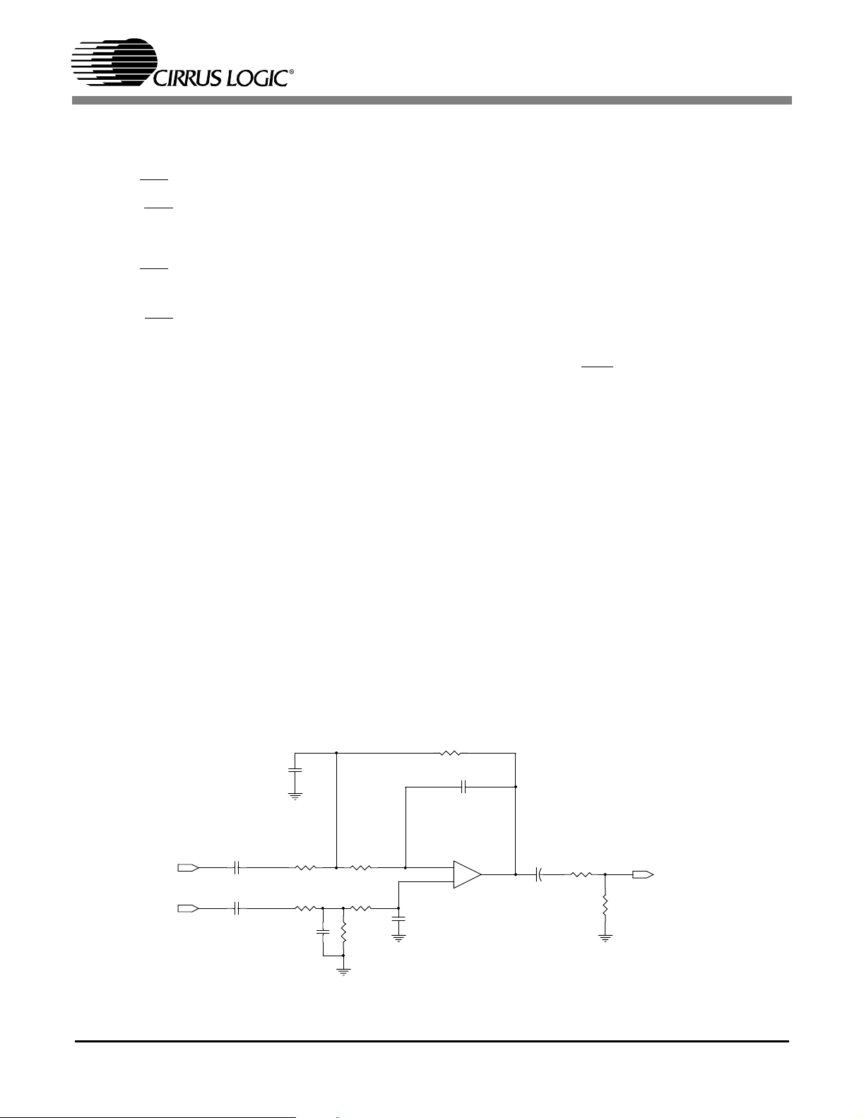
Figure 3. CS4392 Output Filter ....................................................................................................... 9
Figure 4. Format 0, Left Justified up to 24-Bit Data.......................................................................11
Figure 5. Format 1, I2S up to 24-Bit Data ..................................................................................... 11
Figure 6. Format 2, Right Justified 16-Bit Data
Format 3, Right Justified 24-Bit Data
Format 4, Right Justified 20-Bit Data. (Available in Control Port Mode only)
Format 5, Right Justified 18-Bit Data. (Available in Control Port Mode only)................ 11
Figure 7. De-Emphasis Curve ....................................................................................................... 12
Figure 8. Control Port Timing, I2C Mode....................................................................................... 15
Figure 9. Control Port Timing, SPI mode ...................................................................................... 16
Figure 10. De-Emphasis Curve .....................................................................................................19
Figure 11. ATAPI Block Diagram ..................................................................................................21
Figure 12. Single Speed (fast) Stopband Rejection ...................................................................... 28
Figure 13. Single Speed (fast) Transition Band ............................................................................ 28
Figure 14. Single Speed (fast) Transition Band (detail) ................................................................ 28
Figure 15. Single Speed (fast) Passband Ripple .......................................................................... 28
Figure 16. Single Speed (slow) Stopband Rejection ..................................................................... 28
Figure 17. Single Speed (slow) Transition Band ........................................................................... 28
Figure 18. Single Speed (slow) Transition Band (detail) ............................................................... 29
Figure 19. Single Speed (slow) Passband Ripple ......................................................................... 29
Figure 20. Double Speed (fast) Stopband Rejection..................................................................... 29
Figure 21. Double Speed (fast) Transition Band ........................................................................... 29
Figure 22. Double Speed (fast) Transition Band (detail) ............................................................... 29
Figure 23. Double Speed (fast) Passband Ripple ......................................................................... 29
Figure 24. Double Speed (slow) Stopband Rejection ................................................................... 30
Figure 25. Double Speed (slow) Transition Band.......................................................................... 30
Figure 26. Double Speed (slow) Transition Band (detail).............................................................. 30
Figure 27. Double Speed (slow) Passband Ripple........................................................................ 30
Figure 28. Quad Speed (fast) Stopband Rejection ....................................................................... 30
Figure 29. Quad Speed (fast) Transition Band..............................................................................30
Figure 30. Quad Speed (fast) Transition Band (detail).................................................................. 31
Figure 31. Quad Speed (fast) Passband Ripple............................................................................ 31
Figure 32. Quad Speed (slow) Stopband Rejection ...................................................................... 31
Figure 33. Quad Speed (slow) Transition Band ............................................................................31
Figure 34. Quad Speed (slow) Transition Band (detail) ................................................................ 31
Figure 35. Quad Speed (slow) Passband Ripple .......................................................................... 31
Figure 36. Serial Mode Input Timing ............................................................................................. 32
Figure 37. Direct Stream Digital - Serial Audio Input Timing......................................................... 33
Figure 38. I2C Mode Control Port Timing...................................................................................... 34
Figure 39. SPI Control Port Timing ............................................................................................... 35
CS4392
4 DS459PP2
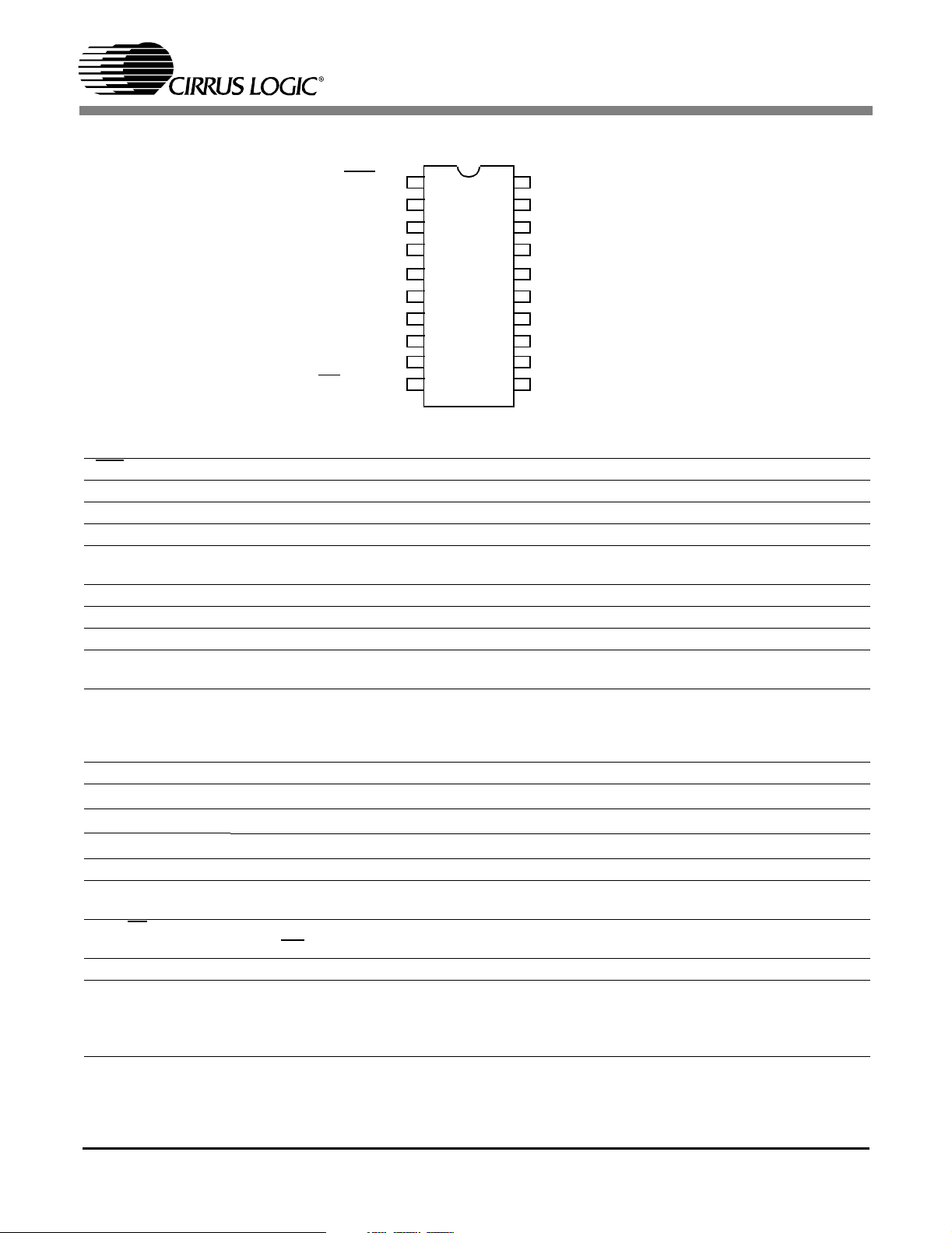
1. PIN DESCRIPTION - PCM DATA MODE
CS4392
RST AMUTEC
VL AOUTA-
SDATA AOUTA+
SCLK VA
LRCK AGND
MCLK AOUTB+
M3 AOUTB-
(SCL/CCLK) M2 BMUTEC
(SDA/CDIN) M1 CMOUT
(AD0/CS
RST 1 Reset (Input) - Powers down device and resets all internal registers to their default settings.
VL 2 Logic Power (Input) - Positive power for the digital input/output.
SDATA 3 Serial Audio Data (Input) - Input for two’s complement serial audio data.
SCLK 4 Serial Clock (Input/Output) - Serial clock for the serial audio interface.
LRCK 5 Left Right Clock (Input/Output) - Determines which channel, Left or Right, is currently active on the
serial audio data line.
MCLK 6 Master Clock (Input) - Clock source for the delta-sigma modulator and digital filters.
FILT+ 11 Positive Voltage Reference (Output) - Positive reference voltage for the internal sampling circuits.
CMOUT 12 Common Mode Voltage (Output) - Filter connection for internal quiescent voltage.
AMUTEC
BMUTEC
AOUTBAOUTB+
AOUTA+
AOUTA
AGND 16 Ground (Input)
VA
Control Port Mode Definitions
M3
SCL/CCLK 8 Serial Control Port Clock (Input) - Serial clock for the serial control port.
SDA/CDIN 9 Serial Control Data (Input/Output) - SDA is a data I/O line in I
AD0/CS
Stand-Alone Mode Definitions
M3
M2
M1
M0
20
13
14
15
18
19
17 Analog Power (Input) - Positive power for the analog section.
10 Address Bit 0 (I2C) / Control Port Chip Select (SPI) (Input/Output)-AD0isachipaddresspininI2C
10
Mute Control (Output) - The Mute Control pin goes high during power-up initialization, reset, muting,
power-down or if the master clock to left/right clock frequency ratio is incorrect.
Differential Analog Output (Outputs) - The full scale differential analog output level is specified in the
Analog Characteristics specification table.
7 Mode Selection (Input) - This pins should be tied to GND level during control port mode.
the control port interface in SPI mode.
mode; CS
Mode Selection (Input) - Determines the operational mode of the device.
7
8
9
)M0 FILT+
is the chip select signal for SPI format.
1
2
3
4
5
6
7
8
9
10
20
19
18
17
16
15
14
13
12
11
2
C mode. CDIN is the input data line for
DS459PP2 5
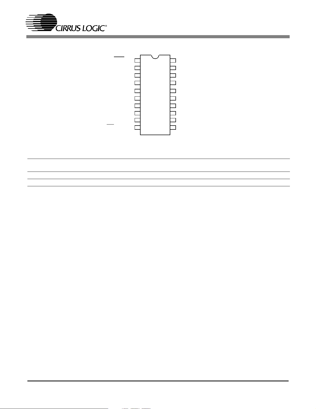
1.1 PIN DESCRIPTION - DSD mode
CS4392
RST AMUTEC
VL AOUTADSD_A AOUTA+
DSD_B VA
DSD_MODE AGND
MCLK AOUTB+
DSD_SCLK AOUTB-
(SCL/CCLK) M2 BMUTEC
(SDA/CDIN) M1 CMOUT
(AD0/CS
DSD_A
DSD_B
DSD_Mode 5 DSD Mode (Input) - In stand alone mode, this pin must be set to a logic ‘1’ for operation of DSD Mode.
DSD_SCLK 7 DSD Serial Clock (Input/Output) - Serial clock for the Direct Stream Digital audio interface.
3
DSD Data (Input) - Input for Direct Stream Digital serial audio data.
4
)M0 FILT+
1
2
3
4
5
6
7
8
9
10
20
19
18
17
16
15
14
13
12
11
6 DS459PP2
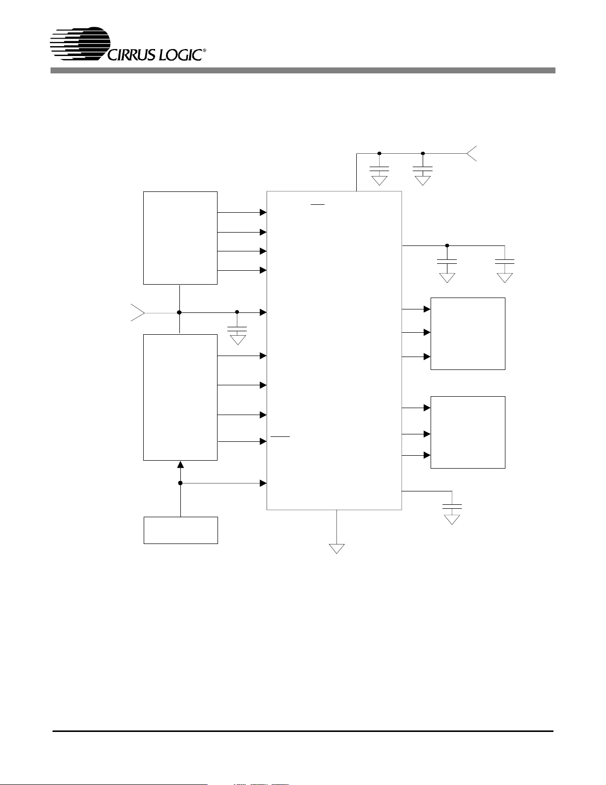
2. TYPICAL CONNECTION DIAGRAMS
CS4392
Logic Power
+5V to 1.8V
Mode
Select
(Control Port)
*
0.1 µf
Audio
Data
Processor
*
10
M0 (AD0/CS)
9
M1 (SDA/CDIN
8
M2 (SCL/CCLK)
7
M3
2
VL
5
LRCK
4
SCLK
3
SDATA
1
RST
17
)
CS4392
VA
AOUTA-
AMUTEC
AOUTA+
AOUTB-
BMUTEC
AOUTB+
0.1 µf
FILT+
19
20
18
14
13
15
11
µ
f+
1.0
0.1 µf 10 µf
Analog
Conditioning
&
Mute
Analog
Conditioning
&
Mute
+5V Analog
+
External Clock
6
MCLK
AGND
CMOUT
16
12
+
1.0 µf
Figure 1. Typical Connection Diagram - PCM Mode
* A high logic level for all digital inputs should not exceed VL.
DS459PP2 7
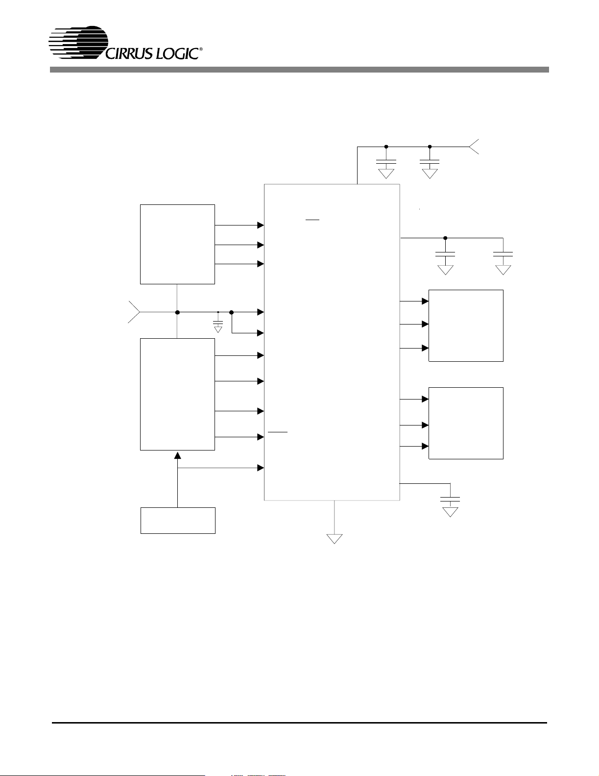
Logic Power
+5V to 1.8V
Mode
Select
(Control Port)
0.1 µf
10
M0 (AD0/CS)
9
M1 (SDA/CDIN)
8
M2 (SCL/CCLK)
2
VL
5
DSD_MODE
7
DSD_CLK
CS4392
17
VA
AMUTEC
AOUTA+
FILT+
AOUTA-
0.1 µf
19
20
18
11
CS4392
+5V Analog
µ
1.0
f+
0.1µf 10µf
Analog
Conditio ning
&
Mute
+
Audio
Data
Processor
*
External Clock
4
3
1
6
DSD_B
DSD_A
RST
MCLK
AOUTB-
BMUTEC
AOUTB+
CMOUT
AGND
16
Figure 2. Typical Connection Diagram - DSD Mode
* A high logic level for all digital inputs should not exceed VL.
14
13
15
12
Analog
Conditioning
&
Mute
1.0 µf
+
8 DS459PP2
3. APPLICATIONS
3.1 Recommended Power-up Sequence for Hardware Mode
1) Hold RST low until the power supplies, master, and left/right clocks are stable.
CS4392
2) Bring
RST high. After 10ms the device will begin normal operation.
3.2 Recommended Power-up Sequence and Access to Control Port Mode
1) Hold RST low until the power supply, master, and left/right clocks are stable. In this state, the control
port is reset to its default settings and FILT+ will remain low.
2) Bring
RST high. The device will remain in a low power state with FILT+ low and the control port is
accessible.
3) Write 30h to register 05h within 10 ms cycles following the release of RST
. If after 10ms the control
port has not been initiated with this command, the device will enter stand-alone mode. The CPEN bit,
however, may be written at any time after 10ms. It is recommended to write CPEN before 10ms in order to reduce the possibility of any extraneous click or pop noise from occurring.
4) The desired register settings can be loaded while keeping the PDN bit set to 1.
5) Set the PDN bit to 0. This will initiate the power-up sequence which requires approximately 10 µS.
3.3 Analog Output and Filtering
The application note “Design Notes for a 2-Pole Filter with Differential Input” discusses the second-order
Butterworth filter and differential to single-ended converter as seen in Figure 3. An alternate configuration
can be seen on the CDB4392. This alternate filter configuration accounts for the differing AC loads on the
+ and - differential output pins which are normally present in a circuit like Figure 3. It also shows an AC
coupling configuration which reduces the number of required AC coupling capacitors to 2 caps per channel. The circuit in figure 3 may also be DC coupled, however the filter on the CDB4392 must be
AC coupled. The CS4392 is a linear phase design and does not include phase or amplitude compensation
for an external filter. Therefore, the DAC system phase and amplitude response will be dependent on the
external analog circuitry.
3.32k
2700 pF
680 pF
Aout -
Aout +
10 uF 560
10 uF
3.01k 1.58k
3.01k
2700 pF
R17
3.32k
1.58k
C10
680 pF
-
2
1
+
3
10 uF
47k
Analog_Out
Figure 3. CS4392 Output Filter
DS459PP2 9
CS4392
3.4 Interpolation Filter
To accommodate the increasingly complex requirements of digital audio systems, the CS4392 incorporates selectable interpolation filters for each mode of operation. A fast and a slow roll-off filter is available
in each of Single, Double, and Quad Speed modes. These filters have been designed to accommodate a
variety of musical tastes and styles. Bit 5 of the Mode Control 3 register (06h) is used to select which filter
is used. Filter specifications can be found in Section 8, and filter response plots can be found in Figures 12
to 35.
In stand-alone mode, only the fast roll-off filter is available.
3.5 System Clocking
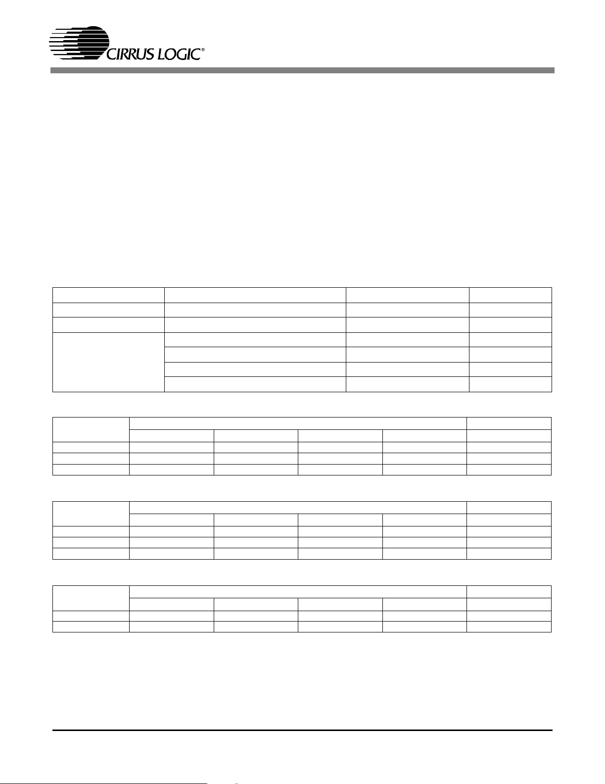
The required MCLK to LRCK and suggested SCLK to LRCK ratios are outlined in table 1. MCLK can be
at any phase in regards to LRCK and SCLK. SCLK, LRCK and SDATA must meet the phase and timing
relationships outlined in Section 7. Some common MCLK frequencies have been outlined in tables 2 to 4.
MCLK/LRCK SCLK/LRCK LRCK
Single Speed 256, 384, 512, 768, 1024* 32, 48, 64, 96, 128 Fs
Double Speed 128, 192, 256, 384, 512* 32, 48, 64 Fs
64 32 (16 bits only) Fs
Quad Speed
96 32, 48 Fs
128, 256* 32, 64 Fs
192 32, 48, 64, 96 Fs
Tab le 1. C lo ck Ra ti os
Sample Rate
(kHz)
32 8.1920 12.2880 16.3840 24.5760 32.7680
44.1 11.2896 16.9344 22.5792 33.8688 45.1584
48 12.2880 18.4320 24.5760 36.8640 49.1520
Sample Rate
(kHz)
64 8.1920 12.2880 16.3840 24.5760 32.7680
88.2 11.2896 16.9344 22.5792 33.8688 45.1584
96 12.2880 18.4320 24.5760 36.8640 49.1520
Sample Rate
(kHz)
176.4 11.2896 16.9344 22.5792 33.8688 45.1584
192 12.2880 18.4320 24.5760 36.8640 49.1520
*Note:These clocking ratios are only available in Control Port Mode when the MCLK Divide bit is enabled.
256x 384x 512x 768x 1024x*
Table 2. Single Speed (4 to 50 kHz sample rates) Common Clock Frequencies
128x 192x 256x 384x 512x*
Table 3. Double Speed (50 to 100 kHz sample rates) Common Clock Frequencies
64x 96x 128x 192x 256x*
Table 4. Quad Speed (100 to 200 kHz sample rates) Common Clock Frequencies
MCLK (MHz) See Note
MCLK (MHz) See Note
MCLK (MHz) See Note
10 DS459PP2
CS4392
3.6 Digital Interface Format
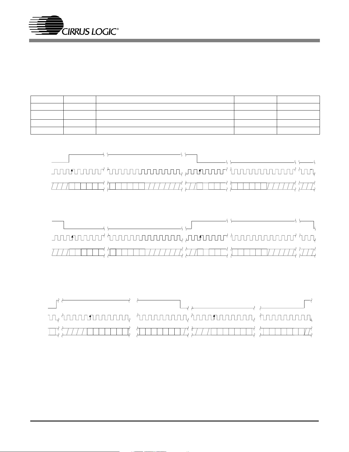
The device will accept audio samples in several digital interface formats as illustrated in Tables 5 and 8.
The desired format is selected via the M0 and M1 pins for stand alone mode, and through the DIF2:0 bits
in the control port. For an illustration of the required relationship between the Left/Right Clock, Serial
Clock and Serial Audio Data, see Figures 4-6.
M1 M0 DESCRIPTION FORMAT FIGURE
00
01
10
11
Left Justified, up to 24-bit data
2
S, up to 24-bit data
I
Right Justified, 16-bit Data
Right Justified, 24-bit Data
Table 5. Digital Interface Format, Stand-Alone Mode Options
04
15
26
36
LRCK
SCLK
SDATA +3 +2 +1
MSB
-1 -2 -3 -4 -5 +3 +2 +1
Left Channel
+5 +4
Figure 4. Format 0, Left Justified up to 24-Bit Data
LRCK
SCLK
SDATA +3 +2 +1
MSB
-1 -2 -3 -4 -5 +3 +2 +1
Left Channel
+5 +4
Figure 5. Format 1, I2S up to 24-Bit Data
LRCK
SCLK
Left Channel
LSB
LSB
MSB
-1 -2 -3 -4
MSB
-1 -2 -3 -4
Right Channel
+5 +4
Right C hannel
+5 +4
Right Channel
LSB
LSB
SDATA
LSB +5 +4 +3 +2
MSB -1 -2 -3 -4 -5
32 clocks
-6 +6
+6
+5 +4 +3 +2
+1
LSB
-1 -2 -3 -4
MSB
-5
-6
+1
LSB
Figure 6. Format 2, Right Justified 16-Bit Data
Format 3, Right Justified 24-Bit Data
Format 4, Right Justified 20-Bit Data. (Available in Control Port Mode only)
Format 5, Right Justified 18-Bit Data. (Available in Control Port Mode only)
DS459PP2 11
CS4392
3.7 De-Emphasis
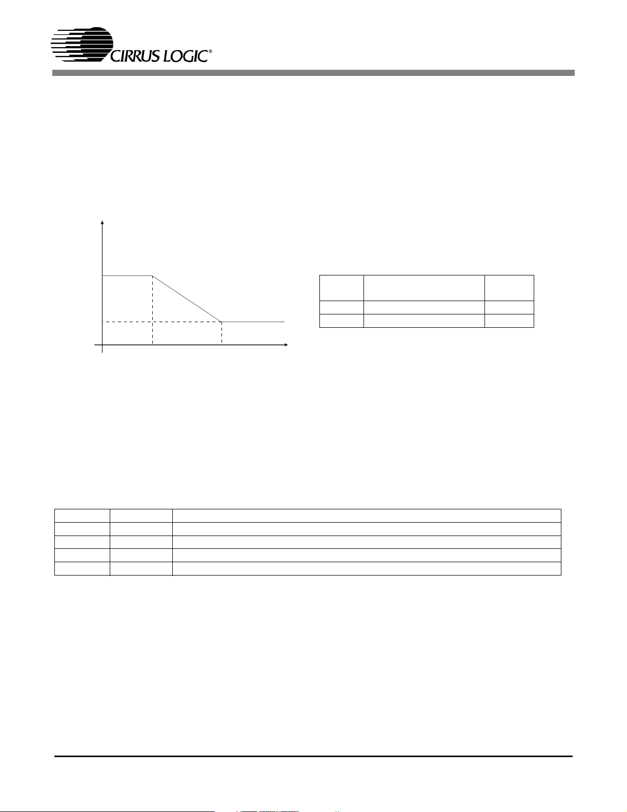
The device includes on-chip digital de-emphasis. Figure 7 shows the de-emphasis curve for FSequal to
44.1 kHz. The frequency response of the de-emphasis curve will scale proportionally with changes in sample rate, F
control port mode.
The de-emphasis feature is included to accommodate audio recordings that utilize 50/15 µS pre-emphasis
equalization as a means of noise reduction.
De-emphasis is only available in Single Speed Mode.
Gain
-10dB
. Please see Table 5 for the desired de-emphasis control for Stand-alone mode and Table 10 for
s
dB
T1=50 µs
0dB
T2 = 15 µs
M2
(DEM)
0
1
Table 5. De-Emphasis Select, Stand-Alone Mode
DESCRIPTION FIGURE
No De-Emphasis
De-Emphasis Enabled
7
F1 F2
3.183 kHz 10.61 kHz
Figure 7. De-Emphasis Curve
Frequency
3.8 Oversampling Modes
The CS4392 operates in one of three oversampling modes based on the input sample rate. Mode selection
is determined by the M3 and M2 pins in Stand-Alone mode or the FM bits in Control Port mode. SingleSpeed mode supports input sample rates up to 50 kHz and uses a 128x oversampling ratio. Double-Speed
mode supports input sample rates up to 100 kHz and uses an oversampling ratio of 64x. Quad-Speed mode
supports input sample rates up to 200 kHz and uses an oversampling ratio of 32x
M3 M2 DESCRIPTION
00
01
10
11
Single-Speed without De-Emphasis (4 to 50 kHz sample rates)
Single-Speed with 44.1kHz De-Emphasis
Double-Speed (50 to 100 kHz sample rates)
Quad-Speed (100 to 200 kHz sample rates)
Table 6. Mode Selection, Stand-Alone Mode Options
12 DS459PP2
CS4392
3.9 Using DSD mode
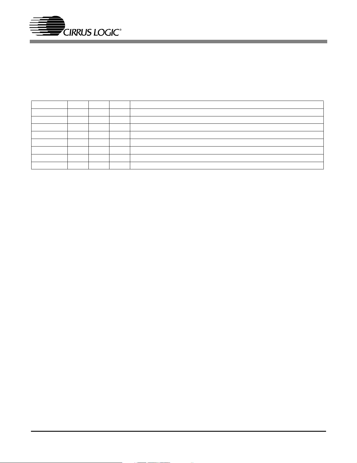
In stand-alone mode, DSD operation is selected by holding DSD_EN(LRCK) high and applying the DSD
data and clocks to the appropriate pins. The M2:0 pins set the expected DSD rate and MCLK ratio.
In control-port mode the FM bits set the device into DSD mode (DSD_EN pin is not required to be held
high). The DIF register then controls the expected DSD rate and MCLK ratio.
DSD_Mode M2 M1 M0 DESCRIPTION
1000
1001
1010
1011
1100
1101
1110
1111
Table 7. Direct Stream Digital (DSD), Stand-Alone Mode Options
3.10 Mute Control
64x oversampled DSD data with a 4x MCLK to DSD data rate
64x oversampled DSD data with a 6x MCLK to DSD data rate
64x oversampled DSD data with a 8x MCLK to DSD data rate
64x oversampled DSD data with a 12x MCLK to DSD data rate
128x oversampled DSD data with a 2x MCLK to DSD data rate
128x oversampled DSD data with a 3x MCLK to DSD data rate
128x oversampled DSD data with a 4x MCLK to DSD data rate
128x oversampled DSD data with a 6x MCLK to DSD data rate
The Mute Control pins go high during power-up initialization, reset, or if the Master Clock to Left Right
Clock ratio is incorrect. These pins will also go high following the reception of 8192 consecutive audio
samples of static 0 or -1 on both the left and right channels. A single sample of non-zero data on either
channel will cause the Mute Control pins to go low. These pins are intended to be used as control for an
external mute circuit in order to add off-chip mute capability.
Use of the Mute Control function is not mandatory but recommended for designs requiring the absolute
minimum in extraneous clicks and pops. Also, use of the Mute Control function can enable the system designer to achieve idle channel noise/signal-to-noise ratios which are only limited by the external mute circuit. See the CDB4392 data sheet for a suggested mute circuit.
DS459PP2 13
 Loading...