

CS4382
114 dB, 192 kHz 8-Channel D/A Converter
Features
24-bit Conversion
Up to 192 kHz Sample Rates
114 dB Dynamic Range
-100 dB THD+N
Supports PCM and DSD Data Formats
Selectable Digital Filters
Volume Control with Soft Ramp
– 1 dB Step Size
– Zero Crossing Click-Free Transitions
Dedicated DSD Inputs
Low Clock-Jitter Sensitivity
Simultaneous Support for Two Synchronous
Sample Rates for DVD Audio
μC or Stand-Alone Operation
Description
The CS4382 is a complete 8-channel digital-to-analog
system including digital interpolation, fifth-order deltasigma digital-to-analog conversion, digital de-emphasis, volume control and analog filtering. The advantages
of this architecture include: ideal differential linearity, no
distortion mechanisms due to resistor matching errors,
no linearity drift over time and temperature and a high
tolerance to clock jitter.
The CS4382 is available in a 48-pin LQFP package in
Commercial grade (-10°C to +70°C). The CDB4382
Customer Demonstration Board is also available for device evaluation and implementation suggestions.
Please see “Ordering Information” on page 42 for complete details.
The CS4382 accepts PCM data at sample rates from
4 kHz to 192 kHz, DSD audio data, and operates over a
wide power supply range. These features are ideal for
multi-channel audio systems including DVD players,
SACD players, A/V receivers, digital TV ’s, mixing consoles, effects processors, and automotive audio
systems.
I
SCLK
LR
SCLK
LRCK2
SD IN1
SD IN2
SD IN3
SD IN4
RST
VLS
CK
MCLK
DSDxx
1
1
2
DSD _SCLK(M 3)
2
÷
8
SCL/CCLK (M1)
Serial Port
SDA/CDIN(M2) AD0/CS(M0)
Control Port(Stand-Alone Mode Select)
Volume Control
Mixer
Volume Control
Volume Control
Mixer
Volume Control
Volume Control
Mixer
Volume Control
Volume Control
Mixer
Volume Control
GNDVD
Interpolation Filter Analog Filter
Interpolation Filter
Interpolation Filter Analog Filter
Inter polation F ilter
Interpolation Filter Analog Filter
Inter polation F ilter
Interpolation Filter Analog Filter
Inter polation F ilter
GND
VLC
VA
MUTEC1
Mute Control
ΔΣ
DAC
ΔΣ
DAC
ΔΣ
DAC
ΔΣ
DAC
ΔΣ
DAC
ΔΣ
DAC
ΔΣ
DAC
ΔΣ
DAC
External
MU TEC234
Analog Filter
Analog Filter
Analog Filter
Analog Filter
AOUTA1+
AOUTA1-
AOUTB1+
AOUTB1-
AOUTA2+
AOUTA2-
AOUTB2+
AOUTB2-
AOUTA3+
AOUTA3-
AOUTB3+
AOUTB3-
AOUTA4+
AOUTA4-
B4+
AOUT
AOUTB4-
VQ
FILT+
http://www.cirrus.com
Copyright © Cirrus Logic, Inc. 2008
(All Rights Reserved)
FEB '08
DS514F2

TABLE OF CONTENTS
1. CHARACTERISTICS AND SPECIFICATIONS ..................................................................................... 5
ANALOG CHARACTERISTICS.............................................................................................................5
ANALOG CHARACTERISTICS.............................................................................................................6
POWER AND THERMAL CHARACTERISTICS ................................................................................... 6
ANALOG FILTER RESPONSE ............................................................................................................. 7
DIGITAL CHARACTERISTICS............................ ... ... .... ... ... ... .... ...................................... ... .... ... ... ........ 8
ABSOLUTE MAXIMUM RATINGS........................................................................................................8
RECOMMENDED OPERATING CONDITIONS.................................................................................... 8
SWITCHING CHARACTERISTICS.. ... ... ... ....................................... ... ... .... ... ... .....................................9
DSD - SWITCHING CHARACTERISTICS .......................................................................................... 10
SWITCHING CHARACTERISTICS - CONTROL PORT - I²C
SWITCHING CHARACTERISTICS - CONTROL PORT - SPI™ FORMAT......................................... 12
2. TYPICAL CONNECTION DIAGRAM ............................................................................................... 13
3. REGISTER QUICK REFERENCE .................................... ... ... .... ... ...................................... .... ... ... ...... 15
4. REGISTER DESCRIPTION .... ... ... .... ... ... ... ....................................... ... ... .... ... ... ................................... 16
4.1 Mode Control 1 (Address 01h) ..................................................................................................... 16
4.1.1 Control Port Enable (CPEN) ............................................................................................ 16
4.1.2 Freeze Controls (FREEZE) .............................................................................................. 16
4.1.3 Master Clock Divide Enable (MCLKDIV) ......................................................................... 16
4.1.4 DAC Pair Disable (DACx_DIS) ........................................................................................ 16
4.1.5 Power Down (PDN) .......................................................................................................... 17
4.2 Mode Control 2 (Address 02h) .................................................................................................... 17
4.2.1 Digital Interface Format (DIF) .......................................................................................... 17
4.2.2 Serial Audio Data Clock Source (SDINXCLK) ................................................................. 18
4.3 Mode Control 3 (Address 03h) .................................................................................................... 18
4.3.1 Soft Ramp and Zero Cross Control (SZC) ....................................................................... 18
4.3.2 Single Volume Control (SNGLVOL) ................................................................................. 19
4.3.3 Soft Volume Ramp-Up After Error (RMP_UP) ................................................................. 19
4.3.4 Mutec Polarity (MUTEC+/-) .............................................................................................. 19
4.3.5 Auto-Mute (AMUTE) ........................................................................................................20
4.3.6 Mutec Pin Control (MUTEC) ............................................................................................ 20
4.4 Filter Control (Address 04h) ................. .... ... ... ... .... ... ... ....... ... ... ... ... .... ... ... ... .... ... ... ... ... .... . ........... 20
4.4.1 Interpolation Filter Select (FILT_SEL) ..................... ... ... ... ... .... ...................................... ... 20
4.4.2 De-Emphasis Control (DEM) ........................................................................................... 20
4.4.3 Soft Ramp-Down Before Filter Mode Change (RMP_DN) ...................................... ... ... ... 21
4.5 Invert Control (Address 05h) ....................................................................................................... 21
4.5.1 Invert Signal Polarity (INV_XX) ........................................................................................ 21
4.6 Mixing Control Pair 1 (Channels A1 & B1)(Address 06h)
Mixing Control Pair 2 (Channels A2 & B2)(Address 09h)
Mixing Control Pair 3 (Channels A3 & B3)(Address 0Ch)
Mixing Control Pair 4 (Channels A4 & B4)(Address 0Fh) ......................................................... 21
4.6.1 Channel A Volume = Channel B Volume (A=B) .................. ............. ............. .......... ......... 21
4.6.2 ATAPI Channel Mixing and Muting (ATAPI) .................................................................... 22
4.6.3 Functional Mode (FM) ................................... ... ... .... ... ...................................... .... ... ... ... ... 23
4.7 Volume Control (Addresses 07h, 08h, 0Ah, 0Bh, 0Dh, 0Eh, 10h, 11h) ... ... .... ... ... ... ... .... ... ...... ... 23
4.7.1 Mute (MUTE) ................................................................................................................... 23
4.7.2 Volume Control (xx_VOL) ................................................................................................ 23
4.8 Chip Revision (Address 12h) ....................................................................................................... 24
4.8.1 Part Number ID (PART) [Read Only] ............................................................................... 24
5. PIN DESCRIPTION ....................... .... ... ... ... ... .... ... ....................................... ... ... ... .... ... ......................... 25
6. APPLICATIONS .................................................................................................................................. 28
6.1 Grounding and Power Supply Decoupling .................................................................................... 28
CS4382
®
FORMAT........................................... 11
2 DS514F2

CS4382
6.2 PCM Mode Select ......................................................................................................................... 28
6.3 Recommended Power-Up Sequence ........................................................................................... 28
6.4 Analog Output and Filtering .......................................................................................................... 28
6.5 Interpolation Filter ......................................................................................................................... 28
6.6 Clock Source Selection ................................................................................................................ 29
6.7 Using DSD Mode .......................................................................................................................... 29
7. CONTROL PORT INTERFACE ........................ ... ... ... .... ...................................... .... ... ... ... ... ................ 29
7.1 Enabling the Control Port ............................................................................................................. 30
7.2 Format Selection .......................................................................................................................... 30
7.3 I²C Format .................................................................................................................................... 30
7.3.1 Writing in I²C Format . .... ... ... ... ... .... ...................................... .... ... ... ... ................................ 30
7.3.2 Reading in I²C Format ............................ .... ... ... ... .... ... ... ....................................... ... ... ...... 30
7.4 SPI Format ................................................................................................................................... 30
7.4.1 Writing in SPI .......................................................... ... ... ... ... ............................................. 31
7.5 Memory Address Pointer (MAP) ........................ .......................................................... ................31
7.5.1 INCR (Auto Map Increment Enable) ................................................................................ 31
7.5.2 MAP4-0 (Memory Address Pointer) ................................. ................................................ 32
8. FILTER PLOTS .............................................................................................................................. 33
9. DIAGRAMS ..................................................................................................................... 37
10. PARAMETER DEFINITIONS ............................................................................................................. 40
11. REFERENCES ................................................................................................................................... 40
12. PACKAGE DIMENSIONS ................................................................................................................. 41
13. ORDERING INFORMATION ............................................................................................................. 42
14. REVISION HISTORY ......................................................................................................................... 42
LIST OF FIGURES
Figure 1. Serial Mode Input Timing.............................................................................................................. 9
Figure 2. Direct Stream Digital - Serial Audio Input Timing........................................................................ 10
Figure 3. Control Port Timing - I²C Format................................................................................................. 11
Figure 4. Control Port Timing - SPI Format................................................................................................ 12
Figure 5. Typical Connection Diagram Control Port.......................... ...... ... ... .... ... ... ... .... ... ... ... ... .... ... ... ...... 13
Figure 6. Typical Connection Diagram Stand-Alone.................................................................................. 14
Figure 7. Control Port Timing, I²C Format.................................................................................................. 31
Figure 8. Control Port Timing, SPI Format................................................................................................. 31
Figure 9. Single-Speed (fast) Stopband Rejection..................................................................................... 33
Figure 10. Single-Speed (fast) Transition Band......................................................................................... 33
Figure 11. Single-Speed (fast) Transition Band (detail)............................................................................. 33
Figure 12. Single-Speed (fast) Passband Ripple.................................................................... ... .... ... ......... 33
Figure 13. Single-Speed (slow) Stopband Rejection ........... ... ... ... .... ... ... ....................................... ... ... ...... 33
Figure 14. Single-Speed (slow) Transition Band........................................................................................ 33
Figure 15. Single-Speed (slow) Transition Band (detail)............................................................................ 34
Figure 16. Single-Speed (slow) Passband Ripple...................................................................................... 34
Figure 17. Double-Speed (fast) Stopband Rejection ................................................................................. 34
Figure 18. Double-Speed (fast) Transition Band........................................................................................ 34
Figure 19. Double-Speed (fast) Transition Band (detail)............................................................................ 34
Figure 20. Double-Speed (fast) Passband Ripple...................................................................................... 34
Figure 21. Double-Speed (slow) Stopband Rejection................................................................................35
Figure 22. Double-Speed (slow) Transition Band................ ... ... ... .... ... ...................................... .... ... ... ...... 35
Figure 23. Double-Speed (slow) Transition Band (detail)................. ... ... ... ... .... ...................................... ... 35
Figure 24. Double-Speed (slow) Passband Ripple.................................................................................... 35
Figure 25. Quad-Speed (fast) Stopband Rejection.................... ... .... ... ... ... ... ....................................... ...... 35
Figure 26. Quad-Speed (fast) Transition Band .......................................................................................... 35
Figure 27. Quad-Speed (fast) Transition Band (detail).... ....... ... ... .... ... ... ... ... .... ... ... ... .... ... ... ... ... ....... ... ...... 36
DS514F2 3

Figure 28. Quad-Speed (fast) Passband Ripple........................................................................................ 36
Figure 29. Quad-Speed (slow) Stopband Rejection................................................................................... 36
Figure 30. Quad-Speed (slow) Transition Band......................................................................................... 36
Figure 31. Quad-Speed (slow) Transition Band (detail)............................................................................. 36
Figure 32. Quad-Speed (slow) Passband Ripple....................................................................................... 36
Figure 33. Format 0 - Left Justified up to 24-bit Data................................................................................. 37
Figure 34. Format 1 - I²S up to 24-bit Data................................................................................................ 37
Figure 35. Format 2 - Right Justified 16-bit Data ....................................................................................... 37
Figure 36. Format 3 - Right Justified 24-bit Data ....................................................................................... 37
Figure 37. Format 4 - Right Justified 20-bit Data ....................................................................................... 38
Figure 38. Format 5 - Right Justified 18-bit Data ....................................................................................... 38
Figure 39. De-Emphasis Curve.................................................................................................................. 38
Figure 40. Channel Pair Routing Diagram (x = Channel Pair 1, 2, 3, or 4)................................................ 38
Figure 41. ATAPI Block Diagram (x = channel pair 1, 2, 3, or 4)............................................................... 39
Figure 42. Recommended Output Filter..................................................................................................... 39
LIST OF TABLES
Table 1. Digital Interface Formats - PCM Mode......................................................................................... 17
Table 2. Digital Interface Formats - DSD Mode ......................................................................................... 18
Table 3. ATAPI Decode ............................................................................................................................. 22
Table 4. Example Digital Volume Settings....... ... ....................................................................................... 23
Table 5. Common Clock Frequencies........................................................................................................ 27
Table 6. Digital Interface Format, Stand-Alone Mode Options................................................................... 27
Table 7. Mode Selection, Stand-Alone Mode Options ...............................................................................27
Table 8. Direct Stream Digital (DSD), Stand-Alone Mode Options............................................................ 27
CS4382
4 DS514F2
CS4382
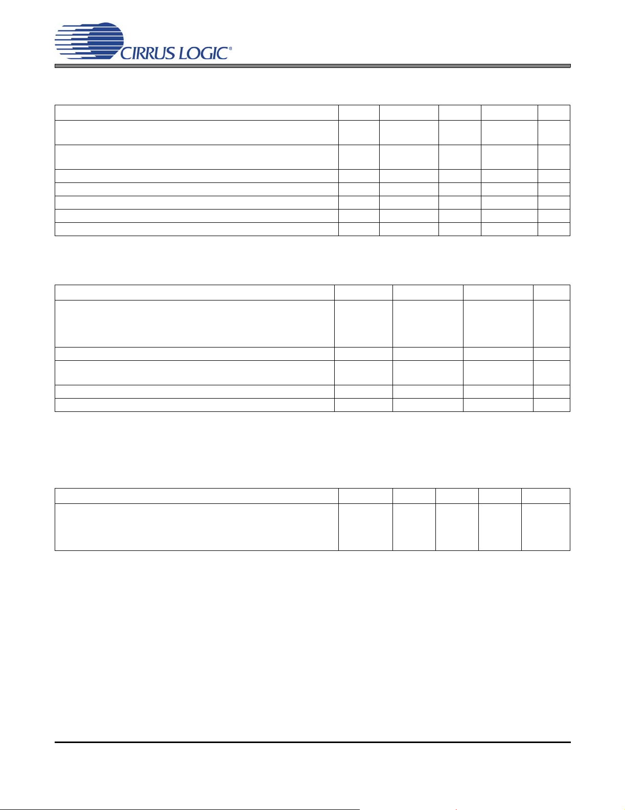
1. CHARACTERISTICS AND SPECIFICATIONS
ANALOG CHARACTERISTICS
(Full-Scale Output Sine Wave, 997 Hz; Measurement Bandwidth 10 Hz to 20 kHz, unless otherwise specified; Test
load R
For Single-Speed Mode, Fs = 48 kHz, SCLK = 3.072 MHz, MCLK = 12.288 MHz;
For Double-Speed Mode, Fs = 96 kHz, SCLK = 6.144 MHz, MCLK = 12.288 MHz;
For Quad-Speed Mode, Fs = 192 kHz, SCLK = 12.288 MHz, MCLK = 24.576 MHz;
For Direct Stream Digital Mode, Fs = 128 x 48 kHz, DSD_SCLK = 6.144 MHz, MCLK = 12.288 MHz).
CS4382-KQZ Dynamic Performance - All PCM modes and DSD (Note 1)
Specified Temperature Range T
Dynamic Range (Note 2) 24-bit unweighted
Total Harmonic Distortion + Noise (Note 2)
Idle Channel Noise / Signal-to-noise ratio - 114 - dB
Interchannel Isolation (1 kHz) - 90 - dB
= 3 kΩ, CL = 100 pF, VA = 5 V, VD = 3.3 V (see Figure 5)
L
Parameters Symbol Min Typ Max Unit
A
A-Weighted
16-bit unweighted
(Note 3) A-Weighted
THD+N
24-bit 0 dB
-20 dB
-60 dB
16-bit 0 dB
(Note 3) -20 dB
-60 dB
-10 - 70 °C
105
108
-
-
-
-
-
-
-
-
111
114
94
97
-100
-91
-51
-94
-74
-34
-
-
-
-
-94
-
-
-
-
-
dB
dB
dB
dB
dB
dB
dB
dB
dB
dB
Notes:
1. CS4382-KQZ parts are tested at 25°C.
2. One-half LSB of triangular PDF dither is added to data.
3. Performance limited by 16-bit quantization noise.
DS514F2 5
CS4382
ANALOG CHARACTERISTICS
(Continued)
Parameters Symbol Min Typ Max Units
Analog Output - All PCM modes and DSD
Full Scale Differential Output Voltage (Note 4) V
Quiescent Voltage V
Max Current from V
Q
FS
I
QMAX
Q
Interchannel Gain Mismatch - 0.1 - dB
Gain Drift - 100 - ppm/°C
Output Impedance (Note 4) Z
AC-Load Resistance R
Load Capacitance C
OUT
L
L
86% V
A
91% V
A
96% V
A
Vpp
- 50% VA-VDC
-1 -μA
- 100 - Ω
3- -kΩ
- - 100 pF
POWER AND THERMAL CHARACTERISTICS
Parameters Symbol Min Typ Max Units
Power Supplies
Power Supply Current normal operation, VA= 5 V
(Note 5) V
V
= 5 V
D
= 3.3 V
D
Interface current, VLC=5 V (Notes 6, 7)
VLS=5 V
power-down state (all supplies) (Note 8)
Power Dissipation (Note 5)
VA = 5 V, VD = 3.3 V normal operation
power-down (Note 8)
VA = 5 V, VD = 5 V normal operation
power-down (Note 8)
Package Thermal Resistance multi-layer
dual-layer
Power Supply Rejection Ratio (Note 9) (1 kHz)
(60 Hz)
I
A
I
D
I
D
I
LC
I
LS
I
pd
θ
JA
θ
JA
θ
JC
PSRR -
-
-
-
-
-
-
-
-
-
-
-
-
-
-
60
45
30
2
84
200
400
1
525
1
48
65
15
60
40
66
70
46
-
-
-
485
-
680
-
-
-
-
-
-
mA
mA
mA
μA
μA
μA
mW
mW
mW
mW
°C/Watt
°C/Watt
°C/Watt
dB
dB
Notes:
4. V
is tested under load RL and includes attenuation due to Z
FS
OUT
5. Current consumption increases with increasing FS within a given speed mode and is signal dependa nt.
Max values are based on highest FS and highest MCLK.
6. I
measured with no external loading on the SDA pin.
LC
7. This specification is violated when the VLC supply is greater than VD and when pin 16 (M1/SDA) is tied
or pulled low. Logic tied to pin 16 needs to be able to sink this current.
8. Power Down Mode is defined as RST
pin = Low with all clock and data lines held static.
9. Valid with the recommended capacitor values on FILT+ and VQ as shown in Figures 5 and 6.
6 DS514F2
CS4382
ANALOG FILTER RESPONSE
Fast Roll-Off Slow Roll-Off
Parameter
Combined Digital and On-chip Analog Filter Response - Single-Speed Mode
Passband (Note 12) to -0.01 dB corner
to -3 dB corner00
Frequency Response 10 Hz to 20 kHz -0.01 - +0.01 -0.01 - +0.01 dB
StopBand .547 - - .583 - - Fs
StopBand Attenuation (Note 13) 90 - - 64 - - dB
Group Delay - 12/Fs - - 6.5/Fs - s
Passband Group Delay Deviation 0 - 20 kHz - - ±0.41/Fs - ±0.14/Fs s
De-emphasis Error (Note 14) Fs = 32 kHz
(Relative to 1 kHz) Fs = 44.1 kHz
Fs = 48 kHz
-
-
-
-
-
-
-
-
.454
.499
±0.23
±0.14
±0.09
(Note 11)
0
0
-
-
-
Combined Digital and On-chip Analog Filter Response - Double-Speed Mode - 96 kHz (Note 11)
Passband (Note 12) to -0.01 dB corner
to -3 dB corner00
Frequency Response 10 Hz to 20 kHz -0.01 - 0.01 -0.01 - 0.01 dB
StopBand .583 - - .792 - - Fs
StopBand Attenuation (Note 13) 80 - - 70 - - dB
Group Delay - 4.6/Fs - - 3.9/Fs - s
Passband Group Delay Deviation 0 - 20 kHz - - ±0.03/Fs - ±0.01/Fs s
-
-
.430
.499
0
0
Combined Digital and On-chip Analog Filter Response - Quad-Speed Mode - 192 kHz (Note 11)
Passband (Note 12) to -0.01 dB corner
to -3 dB corner00
Frequency Response 10 Hz to 20 kHz -0.01 - 0.01 -0.01 - 0.01 dB
StopBand .635 - - .868 - - Fs
StopBand Attenuation (Note 13) 90 - - 75 - - dB
Group Delay - 4.7/Fs - - 4.2/Fs - s
Passband Group Delay Deviation 0 - 20 kHz - - ±0.01/Fs - ±0.01/Fs s
-
-
.105
.490
0
0
Combined Digital and On-chip Analog Filter Response - DSD Mode (Note 11)
Passband (Note 12) to -0.1 dB corner
to -3 dB corner
Frequency Response 10 Hz to 20 kHz - - - -.01 - 0.1 dB
-
-
-
-
-
-
0
0
-
-
-
-
-
-
-
-
-
-
-
(Note 10)
UnitMin Typ Max Min Typ Max
0.417
0.499
±0.23
±0.14
±0.09
.296
.499
.104
.481
20
120
Fs
Fs
dB
dB
dB
Fs
Fs
Fs
Fs
kHz
kHz
Notes:
10. Slow Roll-Off interpolation filter is only available in Control Port Mode.
11. Filter response is not tested but is guaranteed by design.
12. Response is clock dependent and will scale with Fs. Note that the response plots (Figures 9 to 32) have
been normalized to Fs and can be de-normalized by multiplying the X-axis scale by Fs.
13. Single and Double-Speed Mode Measureme nt Bandwidth is from stopband to 3 Fs.
Quad-Speed Mode Measurement Bandwidth is from stopband to 1.34 Fs.
14. De-emphasis is available only in Single-Speed Mode; Only 44.1 kHz De-emphasis is available in StandAlone Mode
DS514F2 7
CS4382
DIGITAL CHARACTERISTICS
(For KQZ TA = -10°C to +70°C; VLC = VLS = 1.8 V to 5.5 V)
Parameters Symbol Min Typ Max Units
High-Level Input Voltage Serial Data Port
Control Port
Low-Level Input Voltage Serial Data Port
Control Port
Input Leakage Current (Note 7) I
Input Capacitance - 8 - pF
Maximum MUTEC Drive Current - 3 - mA
MUTEC High-Level Output Voltage V
MUTEC Low-Level Output Voltage V
V
IH
V
IH
V
IL
V
IL
in
OH
OL
70% VLS
70% VLC
-
-
--±10μA
-VA-V
-0-V
-
-
-
-
-
-
20% VLS
20% VLC
V
V
V
V
ABSOLUTE MAXIMUM RATINGS
(GND = 0 V; all voltages with respect to ground.)
Parameters Symbol Min Max Units
DC Power Supply Analog power
Digital internal power
Serial data port interface power
Control port interface powe r
Input Current, Any Pin Except Supplies I
Digital Input Voltage Serial data port interface
Control port interface
Ambient Operating Temperature (power applied) T
Storage Temperature T
WARNING: Operation at or beyond these limits may result in permanent damage to the device. Normal operation
is not guaranteed at these extremes.
VLS
VLC
V
IND-S
V
IND-C
VA
VD
stg
-0.3
-0.3
-0.3
-0.3
in
A
-±10mA
-0.3
-0.3
-55 125 °C
-65 150 °C
6.0
6.0
6.0
6.0
VLS+ 0.4
VLC+ 0.4
V
V
V
V
V
V
RECOMMENDED OPERATING CONDITIONS
(GND = 0 V; all voltages with respect to ground.)
Parameters Symbol Min Typ Max Units
DC Power Supply Analog power
Digital internal power
Serial data port interface power
Control port interface powe r
8 DS514F2
VA
VD
VLS
VLC
4.5
3.0
1.8
1.8
5.0
3.3
5.0
5.0
5.5
5.5
5.5
5.5
V
V
V
V
CS4382
SWITCHING CHARACTERISTICS
(For KQZ TA = -10°C to +70°C; VLS = 1.8 V to 5.5 V; Inputs: Logic 0 = GND, Logic 1 = VLS, CL = 30 pF)
Parameters Symbol Min Typ Max Units
MCLK Frequency (Note 15)
Single-Speed Mode 1.024 - 51.2 MHz
Double-Speed Mode 6.400 - 51.2 MHz
Quad-Speed Mode 6.400 - 51.2 MHz
MCLK Duty Cycle 405060%
Input Sample Rate Single-Speed Mode
Double-Speed Mode
Quad-Speed Mode
LRCK Duty Cycle 45 50 55 %
SCLK Pulse Width Low t
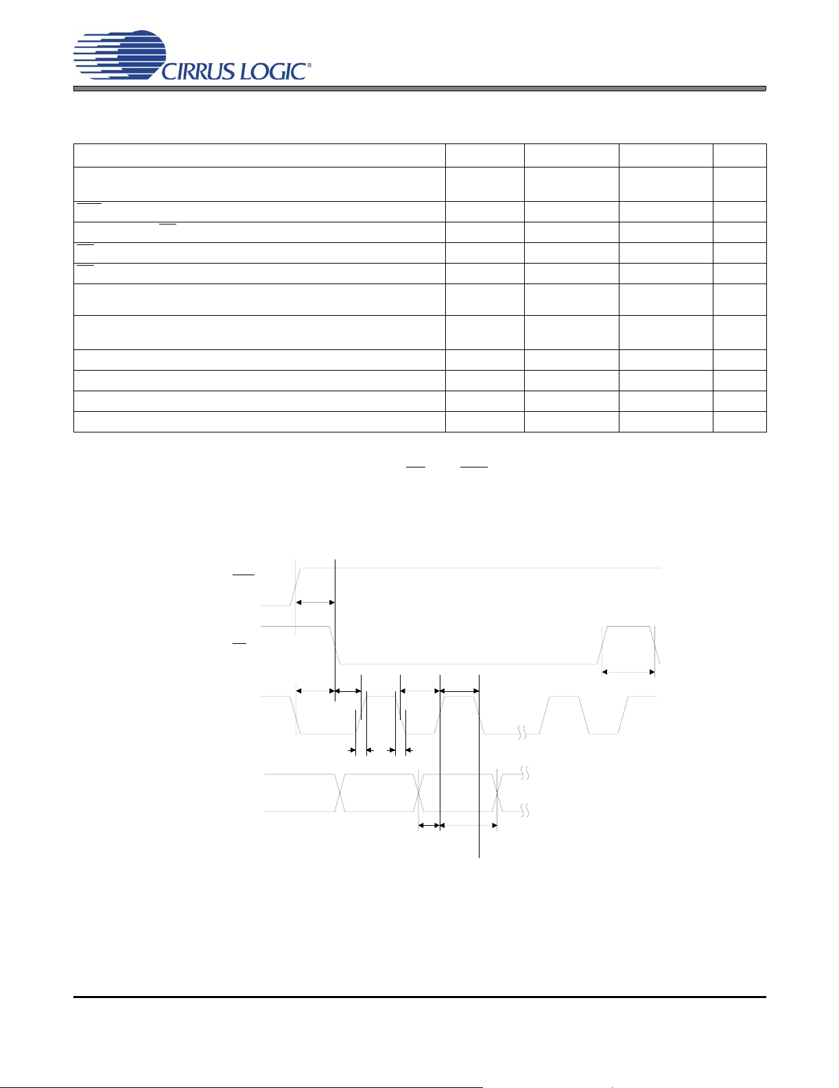
SCLK Pulse Width High t
SCLK Period
(Note 16)
SCLK rising to LRCK edge delay t
SCLK rising to LRCK edge setup time t
SDATA valid to SCLK rising setup time t
SCLK rising to SDATA hold time t
LRCK1 to LRCK2 frequency ratio (Note 17) 0.25 1.00 4.00
Fs
Fs
Fs
sclkl
sclkh
t
sclkw
t
sclkw
slrd
slrs
sdlrs
sdh
4
50
100
-
-
-
50
100
200
20 - - ns
20 - - ns
2
---------------- -
MCLK
4
---------------- -
MCLK
--ns
--ns
20 - - ns
20 - - ns
20 - - ns
20 - - ns
kHz
kHz
kHz
Notes:
.
15. See Table 5 on page 27 for suggested MCLK frequencies.
16. This serial clock is available only in Control Port Mode when the MCLK Divide bit is enabled.
17. The higher frequency LRCK must be an exact inte ger multiple (1, 2, or 4) of the lower frequency LRCK.
LRCK
t
sclkl
t
sdh
t
sclkh
SCLK
SDATA
t
slrd
t
sdlrs
t
slrs
Figure 1. Serial Mode Input Timing
DS514F2 9
CS4382
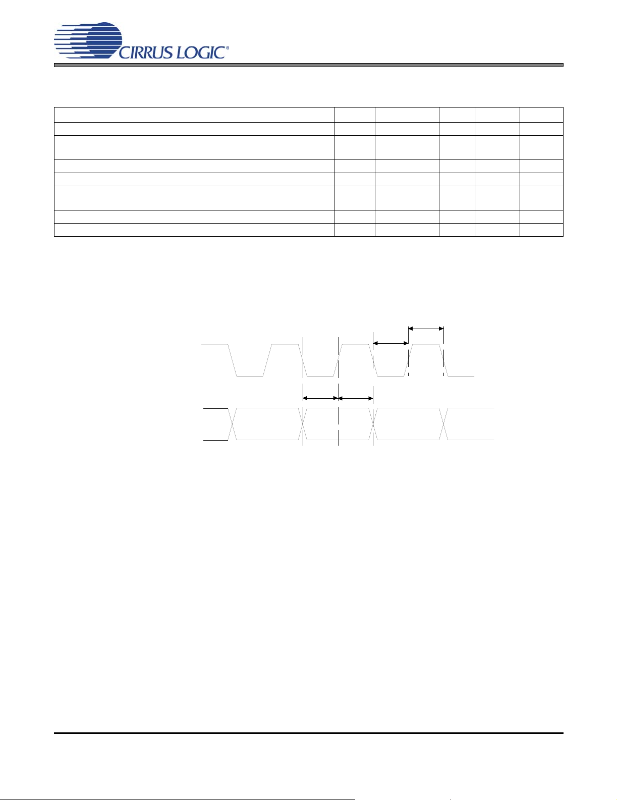
DSD - SWITCHING CHARACTERISTICS
(
For KQZ TA = -10°C to +70°C; Logic 0 = GND; VLS = 1.8 V to 5.5 V; Logic 1 = VLS Volts; CL=30pF)
Parameter Symbol Min Typ Max Unit
Master Clock Frequency (Note 18) 4.096 - 38.4 MHz
MCLK Duty Cycle (All DSD
modes)
DSD_SCLK Pulse Width Low t
DSD_SCLK Pulse Width High t
DSD_SCLK Frequency (64x Oversam-
pled) (128x Oversampled)
DSD_L / _R valid to DSD_SCLK rising setup time t
DSD_SCLK rising to DSD_L or DSD_R hold time t
sclkl
sclkh
sdlrs
sdh
40 50 60 %
20 - - ns
20 - - ns
1.024
2.048
20 - - ns
20 - - ns
-
-
Note:
18. Min is 4 times 64x DSD or 2 times 128x DSD, and Max is 12 times 64x DSD or 6 times 128x DSD. The
proper MCLK to DSD_SCLK ratio must be set either by the DIF registers or the M0:2 pins
t
sclkh
t
sclkl
3.2
6.4
MHz
MHz
DSD_SCLK
DSD_L, DSD_R
Figure 2. Direct Stream Digital - Serial Audio Input Timing
sdlrstsdh
t
10 DS514F2
CS4382
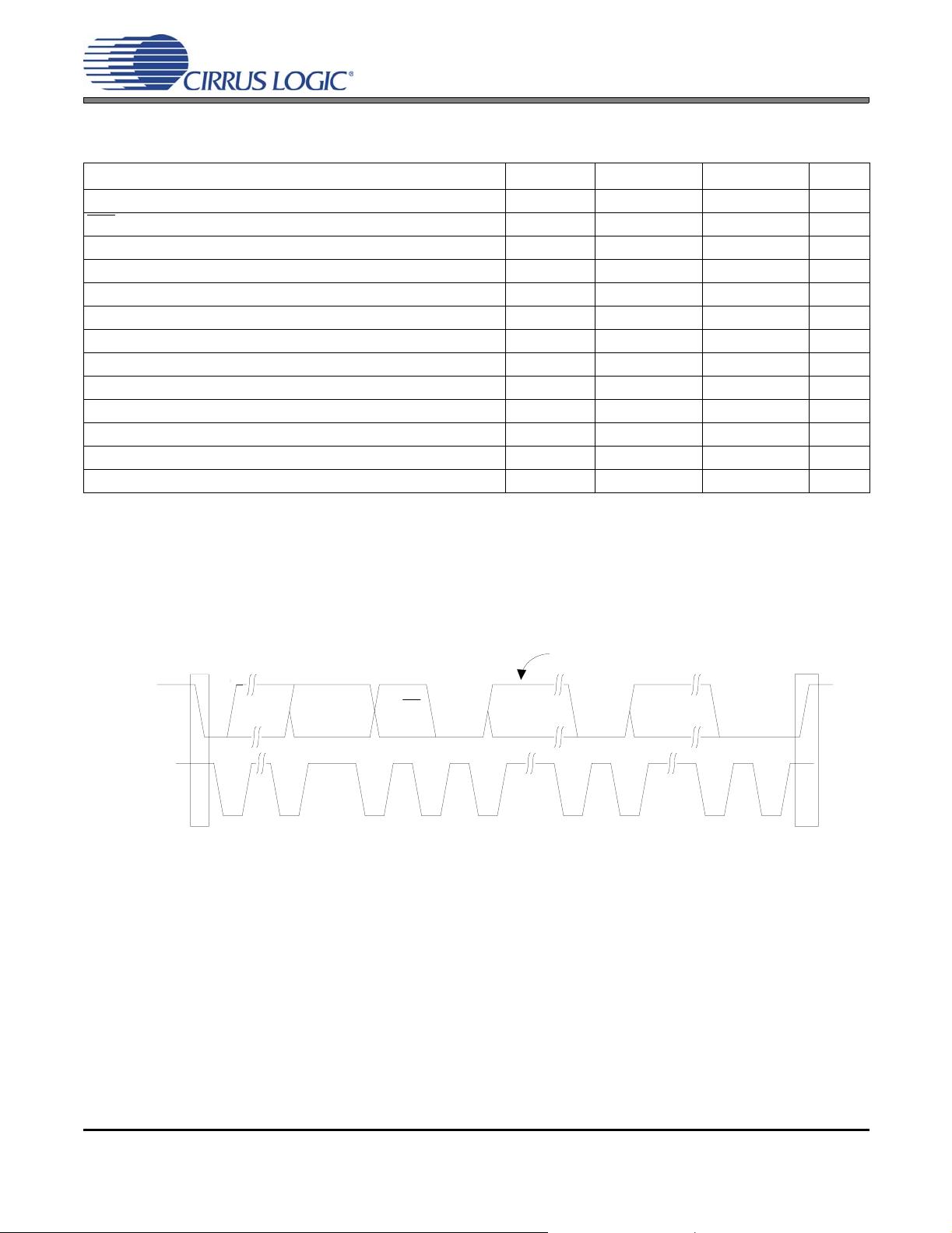
SWITCHING CHARACTERISTICS - CONTROL PORT - I²C® FORMAT
(For KQZ TA = -10°C to +70°C; VLC = 1.8 V to 5.5 V; Inputs: Logic 0 = GND, Logic 1 = VLC, CL=30pF)
Parameter Symbol Min Max Unit
SCL Clock Frequency f
Rising Edge to Start t
RST
Bus Free Time Between Transmissions t
Start Condition Hold Time (prior to first clock pulse) t
Clock Low time t
Clock High Time t
Setup Time for Repeated Start Condition t
SDA Hold Time from SCL Falling (Note 19) t
SDA Setup time to SCL Rising t
Rise Time of SCL and SDA t
Fall Time SCL and SDA t
Setup Time for Stop Condition t
Acknowledge Delay from SCL Falling (Note 20) t
Notes:
19. Data must be held for sufficient time to bridge the transition time, t
20. The acknowledge delay is based on MCLK and can limit the maximum transaction speed.
15
---------------------
21. for Single-Speed Mode, for Double-S peed Mode, for Quad-Speed Mode.
256 Fs×
15
--------------------128 Fs×
hdst
low
high
sust
hdd
sud
rc
fc
susp
ack
scl
irs
buf
, t
, t
rc
fc
- 100 kHz
500 - ns
4.7 - µs
4.0 - µs
4.7 - µs
4.0 - µs
4.7 - µs
0-µs
250 - ns
-1µs
- 300 ns
4.7 - µs
- (Note 21) ns
, of SCL.
fc
15
-----------------64 Fs×
Note 1
SDA
001100
ADDR
AD0
R/W
ACK
DATA
1-8
ACK
DATA
1-8
ACK
SCL
Start
Note: If op e ratio n is a write, th is byte contains the Memory Ad d re ss Pointer, MAP.
Figure 3. Control Port Timing - I²C Format
Stop
DS514F2 11
SWITCHING CHARACTERISTICS - CONTROL PORT - SPI™ FORMAT
(For KQZ TA = -10°C to +70°C; VLC = 1.8 V to 5.5 V; Inputs: Logic 0 = GND, Logic 1 = VLC, CL=30pF)
Parameter Symbol Min Max Unit
MCLK
CCLK Clock Frequency f
Rising Edge to CS Falling t
RST
CCLK Edge to CS
High Time Between Transmissions t
CS
Falling to CCLK Edge t
CS
CCLK Low Time t
CCLK High Time t
CDIN to CCLK Rising Setup Time t
CCLK Rising to DATA Hold Time (Note 23) t
Rise Time of CCLK and CDIN (Note 24) t
Fall Time of CCLK and CDIN (Note 24) t
Falling (Note 22) t
Notes:
22. t
only needed before first falling edge of CS after RST rising edge. t
spi
23. Data must be held for sufficient time to bridge the transition time of CCLK.
24. For F
< 1 MHz.
SCK
sclk
srs
spi
csh
css
scl
sch
dsu
dh
r2
f2
-MHz
500 - ns
500 - ns
1.0 - µs
20 - ns
1
-----------------
MCLK
1
-----------------
MCLK
40 - ns
15 - ns
- 100 ns
- 100 ns
= 0 at all other times.
spi
----------------2
-ns
-ns
CS4382
RST
CS
CCLK
CDIN
t
srs
t
t
spi
t
css
r2
t
t
scl
sch
t
f2
t
t
dsu
dh
Figure 4. Control Port Timing - SPI Format
t
csh
12 DS514F2
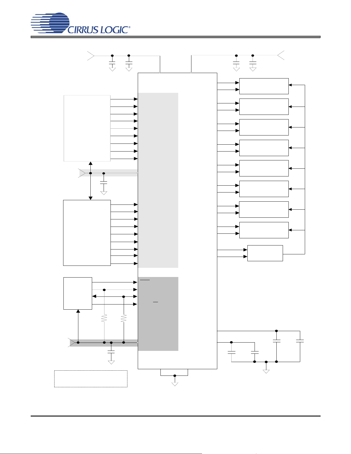
2. TYPICAL CONNECTION DIAGRAM
CS4382
+3.3 V to +5 V
+1.8 V to +5 V
PCM
Digital
Audio
Source
DSD
Audio
Source
1 µF
+
0.1 µF
0.1 µF
6
7
9
10
12
8
11
13
14
43
3
2
1
48
47
46
45
44
42
VD
MCLK
LRCK1
SCLK1
LRCK2
SCLK2
SDIN1
SDIN2
SDIN3
SDIN4
VLS
DSDA1
DSDB1
DSDA2
DSDB2
DSDA3
DSDB3
DSDA4
DSDB4
DSD_SCLK
4
CS4382
32
VA
AOUTA1+
AOUTA1-
AOUTB1+
AOUTB1-
AOUTA2+
AOUTA2-
AOUTB2+
AOUTB2-
AOUTA3+
AOUTA3-
AOUTB3+
AOUTB3-
AOUTA4+
AOUTA4-
AOUTB4+
AOUTB4-
MUTEC1
MUT EC234
0.1 µF
39
40
38
37
35
36
34
33
29
30
28
27
25
26
24
23
41
22
+
1 µF
Analog Conditioning
and Muting
Analog Conditioning
and Muting
Analog Conditioning
and Muting
Analog Conditioning
and Muting
Analog Conditioning
and Muting
Analog Conditioning
and Muting
Analog Conditioning
and Muting
Analog Conditioning
and Muting
Mute
Drive
+5 V
19
RST
Ω
2 K
0.1 µF
15
16
17
18
SCL/CCLK
SDA/CDIN
ADO/CS
VLC
GND
5
GND
31
FILT+
VQ
20
21
0.1 µ
+
F
F
1 µF
+
0.1 µ
47 µF
Micro-
Controller
Ω
2 K
Note*
+1 .8 V to + 5 V
Note: Necessary for I2C
control port operation
Figure 5. Typical Connection Diagram Control Port
DS514F2 13

CS4382
+3 .3 V to + 5 V
VLS
+1 .8 V to + 5 V
Note
PCM
Digital
Audio
Source
DSD
Audio
Source
DSD
1 µF
47 K
Ω
0.1 µF
+
Note
12
11
13
14
DSD
6
7
9
10
8
43
48
47
46
45
44
0.1 µF
3
2
1
MCLK
LRCK 1
SCLK1
LRCK 2
SCLK2
SDIN1
SDIN2
SDIN3
SDIN4
VLS
DSDA1
DSDB1
DSDA2
DSDB2
DSDA3
DSDB3
DSDA4
DSDB4
4
VD
CS4382
32
VA
AOUTA1+
AOUTA1-
AOUTB1+
AOUTB1-
MUTEC1
AOUTA2+
AOUTA2-
AOUTB2+
AOUTB2-
AOUTA3+
AOUTA3-
AOUTB3+
AOUTB3-
AOUTA4+
AOUTA4-
AOUTB4+
AOUTB4-
0.1 µF
39
40
38
37
41
35
36
34
33
29
30
28
27
25
26
24
23
+
1 µF
Analog Conditioning
and Muting
Analog Conditioning
and Muting
Mute
Drive
Analog Conditioning
and Muting
Analog Conditioning
and Muting
Analog Conditioning
and Muting
Analog Conditioning
and Muting
Analog Conditioning
and Muting
Analog Conditioning
and Muting
+5 V
47 K
Configuration
+1 .8 V to + 5 V
Note
used they must be <1 kOhm . If
possible tie VLC to the VD supply
to reduce possible excess current
consum ption from VLC.
Stand-Alone
Mode
VLC
: If series resistors are
Note
Ω
VLC
0.1 µF
42
M3(DSD_SCLK)
15
M2
16
M1
17
M0
19
RST
18
VLC
GND
5
MU TEC234
GND
31
22
20
FILT+
21
VQ
0.1 µ
DSD
Note
1) LRCK1 must be tied to VLS and
2) M3 PCM stand-alone configuration
: For DSD operation:
remain static high.
pin becomes DSD _SC LK
Mute
Drive
+
F
F
1 µF
+
0.1 µ
47 µF
Figure 6. Typical Connection Diagram Stand-Alone
14 DS514F2

CS4382
3. REGISTER QUICK REFERENCE
AddrFunction76543210
01h Mode Control 1 CPEN FREEZE MCLKDIV DAC4_DIS DAC3_DIS DAC2_DIS DAC1_DIS PDN
default00000001
02h Mode Control 2 Reserved DIF2 DIF1 DIF0 SDIN4CLK SDIN3CLK SD IN2 CLK SDIN1CLK
default00000000
03h Mode Control 3 SZC1 SZC0 SNGLVOL RMP_UP MUTEC+/- AMUTE Reserved MUTEC
default10000100
04h Filter Control Reserved Reserved Reserved FILT_SEL Reserved DEM1 DEM0 RMP_DN
default00000000
05h Invert Control INV_B4 INV_A4 INV_B3 INV_A3 INV_B2 INV_A2 INV_B1 INV_A1
default00000000
06h Mixing Control
Pair 1 (AOUTx1)
default00100100
07h Vol. Control A1 A1_MUTE A1_VOL6 A1_VOL5 A1_VOL4 A1_VOL3 A1_VOL2 A1_VOL1 A1_VOL0
default00000000
08h Vol. Control B1 B1_MUTE B1_VOL6 B1_VOL5 B1_VOL4 B1_VOL3 B1_VOL2 B1_VOL1 B1_VOL0
default00000000
09h Mixing Control
Pair 2 (AOUTx2)
default00100100
0Ah Vol. Control A2 A2_MUTE A2_VOL6 A2_VOL5 A2_VOL4 A2_VOL3 A2_VOL2 A2_VOL1 A2_VOL0
default00000000
0Bh Vol. Control B2 B2_MUTE B2_VOL6 B2_VOL5 B2_VOL4 B2_VOL3 B2_VOL2 B2_VOL1 B2_VOL0
default00000000
0Ch Mixing Control
Pair 3 (AOUTx3)
default00100100
0Dh Vol. Control A3 A3_MUTE A3_VOL6 A3_VOL5 A3_VOL4 A3_VOL3 A3_VOL2 A3_VOL1 A3_VOL0
default00000000
0Eh Vol. Control B3 B3_MUTE B3_VOL6 B3_VOL5 B3_VOL4 B3_VOL3 B3_VOL2 B3_VOL1 B3_VOL0
default00000000
0Fh Mixing Control
Pair 4 (AOUTx4)
default00100100
10h Vol. Control A4 A4_MUTE A4_VOL6 A4_VOL5 A4_VOL4 A4_VOL3 A4_VOL2 A4_VOL1 A4_VOL0
default00000000
11h Vol. Control B4 B4_MUTE B4_VOL6 B4_VOL5 B4_VOL4 B4_VOL3 B4_VOL2 B4_VOL1 B4_VOL0
default00000000
12h Chip Revision PART3 PART2 PART1 PART0 Reserved Reserved Reserved Reserved
default1010----
P1_A=B P1ATAPI4 P1ATAPI3 P1ATAPI2 P1ATAPI1 P1ATAPI0 P1FM1 P1FM0
P2_A=B P2ATAPI4 P2ATAPI3 P2ATAPI2 P2ATAPI1 P2ATAPI0 P2FM1 P2FM0
P3_A=B P3ATAPI4 P3ATAPI3 P3ATAPI2 P3ATAPI1 P3ATAPI0 P3FM1 P3FM0
P4_A=B P4ATAPI4 P4ATAPI3 P4ATAPI2 P4ATAPI1 P4ATAPI0 P4FM1 P4FM0
DS514F2 15

CS4382
4. REGISTER DESCRIPTION
Note: All registers are read/write in I²C Mode and write-on ly in SPI, un le ss oth e rwis e no te d.
4.1 Mode Control 1 (Address 01h)
76543210
CPEN FREEZE MCLKDIV DAC4_DIS DAC3_DIS DAC2_DIS DAC1_DIS PDN
00000001
4.1.1 Control Port Enable (CPEN)
Default = 0
0 - Disabled
1 - Enabled
Function:
This bit defaults to 0, allowing the device to power-up in Stand- Alone Mo de. The Co ntrol Por t Mode can
be accessed by setting this bit to 1. This will allow the operation of the device to be controlled by the registers and the pin definitions will conform to Control Port Mode. To accomplish a clean power-up, the user
should write this bit within 10 ms following the release of Reset.
4.1.2 Freeze Controls (FREEZE)
Default = 0
0 - Disabled
1 - Enabled
Function:
This function allows modifications to be made to the registers without the changes taking effect until the
FREEZE is disabled. To make multiple changes in the Control port registers take effect simultaneously,
enable the FREEZE bit, make all register changes, then Disable the FREEZE bit.
4.1.3 Master Clock Divide Enable (MCLKDIV)
Default = 0
0 - Disabled
1 - Enabled
Function:
The MCLKDIV bit enables a circuit which divides the externally applied MCLK signa l by 2 prior to all other
internal circuitry.
4.1.4 DAC Pair Disable (DACx_DIS)
Default = 0
0 - DAC Pair x Enabled
1 - DAC Pair x Disabled
Function:
When the bit is set, the respective DAC channel pair (AOUTAx and AOUTBx) will remain in a reset state.
It is advised that changes to these bits be ma de while th e power- down (PDN ) bit is enabled to elimina te
the possibility of audible artifacts.
16 DS514F2

CS4382
4.1.5 Power Down (PDN)
Default = 1
0 - Disabled
1 - Enabled
Function:
The entire device will enter a low-power state when this function is enabled, and the contents of the control
registers are retained in this mode. The power-down bit defaults to ‘enabled’ on power-up and must be
disabled before normal operation in Control Port Mode can occur.
4.2 Mode Control 2 (Address 02h)
76543210
Reserved DIF2 DIF1 DIF0 SDIN4CLK SDIN3CLK SDIN2CLK SDIN1CLK
00000000
4.2.1 Digital Interface Format (DIF)
Default = 000 - Format 0 (Left Justified, up to 24-bit data)
Function:
These bits select the interface format for the serial audio input. The Functional Mode bits determine
whether PCM or DSD Mode is selected.
PCM Mode: The required relationship between the Le ft/Right clock, serial clock and serial data is defined
by the Digital Interface Format and the options are detailed in Figures 33-38.
Note: While in PCM Mode, the DIF bits should only be changed when th e power-do wn (PDN) bit is set
to ensure proper switching from one mode to another.
DIF2 DIF1 DIF0 DESCRIPTION Format FIGURE
000
001
010
011
100
101
110
111
Left Justified, up to 24-bit data
I²S, up to 24-bit data
Right Justified, 16-bit data
Right Justified, 24-bit data
Right Justified, 20-bit data
Right Justified, 18-bit data
Reserved
Reserved
0 33
1 34
2 35
3 36
4 37
5 38
Table 1. Digital Interface Formats - PCM Mode
DS514F2 17

DSD Mode: The relationship between the oversampling ratio of the DSD audio data and the required
Master clock to DSD data rate is defined by the Digital Interface Format pins. An additional write of 99h
to register 00h and 80h to register 1Ah is required to access the modes denoted with *.
DIF2 DIF1 DIFO DESCRIPTION Note
0 0 0 64x oversampled DSD data with a 4x MCLK to DSD data rate
0 0 1 64x oversampled DSD data with a 6x MCLK to DSD data rate *
0 1 0 64x oversampled DSD data with a 8x MCLK to DSD data rate *
0 1 1 64x oversampled DSD data with a 12x MCLK to DSD data rate *
1 0 0 128x oversampled DSD data with a 2x MCLK to DSD data rate
1 0 1 128x oversampled DSD data with a 3x MCLK to DSD data rate *
1 1 0 128x oversampled DSD data with a 4x MCLK to DSD data rate *
1 1 1 128x oversampled DSD data with a 6x MCLK to DSD data rate *
Table 2. Digital Interface Formats - DSD Mode
4.2.2 Serial Audio Data Clock Source (SDINXCLK)
Default = 0
0 - SDINx clocked by SCLK1 and LRCK1
1 - SDINx clocked by SCLK2 and LRCK2
Function:
CS4382
The SDINxCLK bit specifies which SCLK/LRCK input pair is used to clock in the data on the given SDINx
line. For more details see “Clock Source Selection” on page 29.
4.3 Mode Control 3 (Address 03h)
76543210
SZC1 SZC0 SNGLVOL RMP_UP Reserved AMUTE Reserved MUTEC
10000100
4.3.1 Soft Ramp and Zero Cross Control (SZC)
Default = 10
00 - Immediate Change
01 - Zero Cross
10 - Soft Ramp
11 - Soft Ramp on Zero Crossings
Function:
Immediate Change
When Immediate Change is selected all level changes will take effect immediately in one step.
Zero Cross
Zero Cross Enable dictates that signal level changes, either by attenuation changes or muting, will occur
on a signal zero crossing to minimize audible artifacts. The requested level change will occur after a timeout period between 512 and 1024 sample periods (10.7 ms to 21.3 ms at 48 kHz sample rate) if the signal
does not encounter a zero crossing. The zero cros s function is independently monitored and impleme nted
for each channel.
18 DS514F2

Soft Ramp
Soft Ramp allows level changes, both muting and attenuation, to be implemented by incrementally ramp-
ing, in 1/8 dB steps, from the current level to the new level at a rate of 1 dB per 8 left/right clock periods.
Soft Ramp on Zero Crossing
Soft Ramp and Zero Cross Enable dictates that signal level changes, either by attenuation changes or
muting, will occur in 1/8 dB steps and be implemented on a signal zero crossing. The 1/8 dB level change
will occur after a timeout period between 512 and 1024 sample periods (10.7 ms to 21.3 ms at 48 kHz
sample rate) if the signal does not encounter a zero crossing. The zero cross function is independently
monitored and implemented for each channel.
4.3.2 Single Volume Control (SNGLVOL)
Default = 0
0 - Disabled
1 - Enabled
Function:
The individual channel volume levels are independently controlled by their respective Volume Control
Bytes when this function is disabled. The volume on all channels is determined by the A1 Channel Volume Control Byte, and the other Volume Control Bytes are ignored when this function is enabled.
CS4382
4.3.3 Soft Volume Ramp-Up After Error (RMP_UP)
Default = 0
0 - Disabled
1 - Enabled
Function:
An un-mute will be performed after executing a filter mode change, after a LRCK/MCLK ratio change or
error, and after changing t he Functional Mode. When this feature is enabled, this un-mute is effected,
similar to attenuation changes, by the Soft and Zero Cross bits in the Mode Control 3 register. Whe n disabled, an immediate un-mute is performed in these instances.
Note: For best results, it is recommended that this feature be used in conjunction with the RMP_DN bit.
4.3.4 Mutec Polarity (MUTEC+/-)
Default = 0
0 - Active High
1 - Active Low
Function:
The active polarity of the MUTEC pin(s) is determined by this register. When set to 0 (default), the MUTEC
pins are high when active. When set to 1 the MUTEC pin(s) are low when active.
Note: When the onboard mute circuitry is designed for active low, the MUTEC outputs will be high (un-
muted) for the period of time during reset and before this bit is enabled to 1.
DS514F2 19

4.3.5 Auto-Mute (AMUTE)
Default = 1
0 - Disabled
1 - Enabled
Function:
The Digital-to-Analog converter output will mute following the reception of 8192 consecutive audio sam-
ples of static 0 or -1. A single sample of non-static data will release the mute. Detection and muting is
done independently for each channel. The quiescent voltage on the output will be retained and the Mute
Control pin will go active during the mute period. The muting function is affected, similar to volume control
changes, by the Soft and Zero Cross bits in the Mode Control 3 register.
4.3.6 Mutec Pin Control (MUTEC)
Default = 0
0 - Two Mute control signals
1 - Single mute control signal on MUTEC1
Function:
Selects how the internal mute signals are routed to the MUTEC1 and MUTEC234 pins. When set to ‘0’,
a logical AND of DAC pair 1 mute control signals are output on MUTEC1 and a logical AND of the mute
control signals of DAC pairs 2, 3, and 4 are output on MUTEC234. When set to ‘1’, a logical AND of all
DAC pair mute control signals is output on the MUTEC1 pin, MUTEC234 will remain static. For more information on the use of the mute control function see the MUTEC1 and MUTEC234 pi ns in Section 5. Pin
Description.
CS4382
4.4 Filter Control (Address 04h)
76543210
Reserved Reserved Reserved FIL T_SEL Reserved DEM1 DEM0 RMP_DN
00000000
4.4.1 Interpolation Filter Select (FILT_SEL)
Default = 0
0 - Fast roll-off
1 - Slow roll-off
Function:
This Function allows the user to select whether the interpolation filter has a fast or slow roll off. For filter
characteristics please see Section 1.
4.4.2 De-Emphasis Control (DEM)
Default = 00
00 - Disabled
01 - 44.1 kHz
10 - 48 kHz
11 - 32 kHz
Function:
20 DS514F2

CS4382
Selects the appropriate digital filter to maintain the standard 15 ms/50 ms digital de-emphasis filter response at 32, 44.1 or 48 kHz sample rates. (see Figure 39)
De-emphasis is only available in Single-Speed Mode.
4.4.3 Soft Ramp-Down Before Filter Mode Change (RMP_DN)
Default = 0
0 - Disabled
1 - Enabled
Function:
A mute will be performed prior to executing a filter mode change. When this feature is enabled, this mute
is effected, similar to attenuation changes, by the Soft and Zero Cross bits in the Mode Control 3 register.
When disabled, an immediate mute is performed prior to executing a filter mode change.
Note: For best results, it is recommended that this feature be used in conjunction with the RMP_UP bit.
4.5 Invert Control (Address 05h)
76543210
INV_B4 INV_A4 INV_B3 INV_A3 INV_B2 INV_A2 INV_B1 INV_A1
00000000
4.5.1 Invert Signal Polarity (INV_XX)
Default = 0
0 - Disabled
1 - Enabled
Function:
When enabled, these bits will invert the signal polarity of their respective channels.
4.6 Mixing Control Pair 1 (Channels A1 & B1)(Address 06h)
Mixing Control Pair 2 (Channels A2 & B2)(Address 09h)
Mixing Control Pair 3 (Channels A3 & B3)(Address 0Ch)
Mixing Control Pair 4 (Channels A4 & B4)(Address 0Fh)
76543210
Px_A=B PxATAPI4 PxATAPI3 PxATAPI2 PxATAPI1 PxATAPI0 PxFM1 PxFM0
00100100
4.6.1 Channel A Volume = Channel B Volume (A=B)
Default = 0
0 - Disabled
1 - Enabled
Function:
The AOUTAx and AOUTBx volume levels are independently controlled by the A and the B Channel Vol-
ume Control Bytes when this function is disabled. The volume on both AOUTAx and AOUTBx are determined by the A Channel Attenuation and Volume Control Bytes (per A-B pair), and the B Channel Bytes
are ignored when this function is enabled.
DS514F2 21

4.6.2 ATAPI Channel Mixing and Muting (ATAPI)
Default = 01001 - AOUTAx=aL, AOUTBx=bR (Stereo)
Function:
The CS4382 implements the channel mixing functions of the ATAPI CD-ROM specification. The ATAPI
functions are applied per A-B pair. Refer to Table 3 and Figure 41 for additional information.
ATAPI4 ATAPI3 ATAPI2 ATAPI1 ATAPI0 AOUTAx AOUTBx
00000 MUTE MUTE
00001 MUTE bR
00010 MUTE bL
00011 MUTE b[(L+R)/2]
00100 aR MUTE
00101 aR bR
00110 aR bL
00111 aR b[(L+R)/2]
01000 aL MUTE
01001 aL bR
01010 aL bL
01011 aL b[(L+R)/2]
0 1 1 0 0 a[(L+R)/2] MUTE
01101 a[(L+R)/2] bR
01110 a[(L+R)/2] bL
0 1 1 1 1 a[(L+R)/2] b[(L+R)/2]
10000 MUTE MUTE
10001 MUTE bR
10010 MUTE bL
10011 MUTE [(aL+bR)/2]
10100 aR MUTE
10101 aR bR
10110 aR bL
10111 aR [(bL+aR)/2]
11000 aL MUTE
11001 aL bR
11010 aL bL
11011 aL [(aL+bR)/2]
11100[(aL+bR)/2] MUTE
11101[(aL+bR)/2] bR
11110[(bL+aR)/2] bL
1 1 1 1 1 [(aL+bR)/2] [(aL+bR)/2]
Table 3. ATAPI Decode
CS4382
22 DS514F2

CS4382
4.6.3 Functional Mode (FM)
Default = 00
00 - Single-Speed Mode (4 to 50 kHz sample rates)
01 - Double-Speed Mode (50 to 100 kHz sample rates)
10 - Quad-Speed Mode (100 to 200 kHz sample rates)
11 - Direct Stream Digital Mode
Function:
Selects the required range of input sample rates or DSD Mode. When DSD Mode is selected for any chan-
nel pair then all pairs will switch to DSD Mode.
4.7 Volume Control (Addresses 07h, 08h, 0Ah, 0Bh, 0Dh, 0Eh, 10h, 11h)
76543210
xx_MUTE xx_VOL6 xx_VOL5 xx_VOL4 xx_VOL3 xx_VOL2 xx_VOL1 xx_VOL0
00000000
4.7.1 Mute (MUTE)
Default = 0
0 - Disabled
1 - Enabled
Function:
The Digital-to-Analog converter output will mute when enabled. The quiescent voltage on the output will
be retained. The muting f unction is effected, similar to attenuation changes, by the Soft and Zero Cross
bits. The MUTEC pins will go active during the mute period according to the MUTEC register.
4.7.2 Volume Control (xx_VOL)
Default = 0 (No attenuation)
Function:
The Digital Volume Control registers allow independent control of the signal levels in 1 dB increments
from 0 to -127 dB. Volume settings are decoded as shown in Table 4. The volume changes are implemented as dictated by the Soft and Zero Cross bits. All volume settings less than -127 dB are equivalent
to enabling the MUTE bit.
Binary Code Decimal Value Volume Setting
0000000 0 0 dB
0010100 20 -20 dB
0101000 40 -40 dB
0111100 60 -60 dB
1011010 90 -90 dB
Table 4. Example Digital Volume Settings
DS514F2 23

CS4382
4.8 Chip Revision (Address 12h)
76543210
PART3 PART2 PART1 PART0 Reserved Reserved Reserved Reserved
1010- - - -
4.8.1 Part Number ID (PART) [Read Only]
1010 - CS4382
Function:
This read-only register can be used to identify the model number of the device.
24 DS514F2

5. PIN DESCRIPTION
CS4382
AOUTA1-
VQ
AOUTB1-
AOUTA1+
AOUTB1+
36
35
34
33
32
31
30
29
28
27
26
25
AOUTB4-
AOUTB4+
MUTEC234
DSDA2
DSDB1
DSDA1
VD
GND
MCLK
LRCK1(DSD_EN)
SDIN1
SCLK1
LRCK2
SDIN2
SCLK2
MUTEC1
VLS
M3(DSD_SCLK)
DSDB4
DSDA4
DSDB3
DSDB2
DSDA3
48 47 46 45 44 43 42 41 40 39 38 37
1
2
3
4
5
6
7
8
9
10
11
12
13 14 15 16 17 18 19 20 21 22 23 24
SDIN3
SDIN4
CS4382
M1(SDA/CDIN)
M2(SCL/CCLK)
RST
VLC
FILT+
M0(AD0/CS)
Pin Name # Pin Description
VD 4
GND
MCLK 6
LRCK1
LRCK2
SDIN1
SDIN2
SDIN3
SDIN4
SCLK1
SCLK2
VLC 18
RST
FILT+ 20
VQ 21
Digital Power (Input) - Positive power supply for the digital section. Refer to the Recommended Operating Conditions for appropriate voltages.
5
Ground (Input) - Ground reference. Should be connected to analog ground.
31
Master Clock (Input) - Clock source for the delta-sigma modulator and digital filters. Table 5 illustrates
several standard audio sample rates and the required master clock frequency.
710Left Right Clock (Input) - Determines which channel, Left or Right, is currently active on the serial audio
data line. The frequency of the left/right clock must be at the audio sample rate, Fs.
8
11
Serial Audio Data Input (Input) - Input for two’s complement serial audio data.
13
14
9
Serial Clock (Input) - Serial clock for the serial audio interface.
12
Control Port Power (Input) - Determines the required signal level for the control port. Refer to the Recommended Operating Conditions for appropriate voltages.
Reset (Input) - The device enters a low power mode and all internal registers are reset to their default
19
settings when low.
Positive Voltage Reference (Output) - Positive reference voltage for the internal sampling circuits.
Requires the capacitive decoupling to analog ground, as shown in the Typical Connection Diagram.
Quiescent Voltage (Output) - Filter connection for internal quiesce nt volta ge. VQ must be capacitively
coupled to analog ground, as shown in the Typical Connection Diagram. The nominal voltage level is
specified in the Analog Characteristics and Specifications section. VQ presents an appreciable source
impedance and any current drawn from this pin will alter device performance.
However, VQ can be used to bias the analog circuitry assuming there is no AC signal component and
the DC current is less than the maximum specified in the Analog Characteristics and Specifications section.
AOUTA2AOUTA2+
AOUTB2+
AOUTB2-
VA
GND
AOUTA3AOUTA3+
AOUTB3+
AOUTB3-
AOUTA4-
AOUTA4+
DS514F2 25

Pin Name # Pin Description
Mute Control (Output) - The Mute Control pins go high during power-up initialization, reset, muting,
MUTEC1
MUTEC234
AOUTA1 +,AOUTB1 +,AOUTA2 +,AOUTB2 +,AOUTA3 +,AOUTB3 +,AOUTA4 +,AOUTB4 +,-
VA 32
VLS 43
power-down or if the master clock to left/right clock frequency ratio is incorrect. These pins are intended
41
to be used as a control for external mute circuits to prevent the clicks and pops that can occur in any sin-
22
gle supply system. The use of external mute circuits are not mandatory but may be desired for designs
requiring the absolute minimum in extraneous clicks and pops.
39, 40
38, 37
35, 36
Differential Analog Output (Output) - The full scale differential analog output level is specified in the
34, 33
Analog Characteristics specification table.
29, 30
28, 27
25, 26
24, 23
Analog Power (Input) - Positive power supply for the analog section. Refer to the Recommended Oper-
ating Conditions for appropriate voltages.
Serial Audio Interface Power (Input) - Determines the required signal level for the serial audio inter-
face. Refer to the Recommended Operating Conditions for appropriate voltages.
Control Port Definitions
SCL/CCLK 15
SDA/CDIN 16
AD0/CS
Serial Control Port Clock (Input) - Serial clock for the serial control port. Requires an external pull-up
resistor to the logic interface voltage in
Serial Control Data (Input/Output) - SDA is a data I/O line in I²C Mode and requires an external pull-up
resistor to the logic interface voltage, as shown in the Typical Connection Diagram. CDIN is the input
data line for the control port interface in SPI Mode.
Address Bit 0 (I²C) / Control Port Chip Select (SPI) (Input) - AD0 is a chip address pi n in I²C Mode;
17
CS is the chip select signal for SPI format.
I²C Mode as shown in the Typical Connection Diagram.
CS4382
Stand-Alone Definitions
M0
M1
M2
M3
17
16
Mode Selection (Input) - Determines the operational mode of the device as detailed in Tables 6 and 7.
15
42
DSD Definitions
DSD_SCLK 42 DSD Serial Clock (Input) - Serial clock for the Direct Stream Digital audio interface.
DSD_EN 7
DSDA1
DSDB1
DSDA2
DSDB2
DSDA3
DSDB3
DSDA4
DSDB4
DSD-Enable (Input) - When held at logic ‘1’ the device will enter DSD Mode (Stand-Alone Mode only).
3
2
1
48
Direct Stream Digital Input (Input) - Input for Direct Stream Digital serial audio data.
47
46
45
44
26 DS514F2

CS4382
Mode
(sample-rate range)
Sample
Rate
MCLK (MHz)
(kHz)
MCLK Ratio 256x 384x 512x 768x* 1024x*
Single-Speed
(4 to 50 kHz)
32 8.1920 12.2880 16.3840 24.5760 32.7680
44.1 11.2896 16.9344 22.5792 33.8688 45.1584
48 12.2880 18.4320 24.5760 36.8640 49.1520
MCLK Ratio 128x 192x 256x 384x 512x*
Double-Speed
(50 to 100 kHz)
64 8.1920 12.2880 16.3840 24.5760 32.7680
88.2 11.2896 16.9344 22.5792 33.8688 45.1584
96 12.2880 18.4320 24.5760 36.8640 49.1520
MCLK Ratio 64x 96x 128x 192x 256x*
Quad-Speed
(100 to 200 kHz)
176.4 11.2896 16.9344 22.5792 33.8688 45.1584
192 12.2880 18.4320 24.5760 36.8640 49.1520
Note: *These modes are only available in Control Port Mode by setting the MCLKDIV bit = 1.
Table 5. Common Clock Frequencies
M1
(DIF1)
0 0 Left Justified, up to 24-bit data 0 33
0 1 I²S, up to 24-bit data 1 34
1 0 Right Justified, 16-bit Data 2 35
1 1 Right Justified, 24-bit Data 3 36
M0
(DIF0)
DESCRIPTION FORMAT FIGURE
Table 6. Digital Interface Format, Stand-Alone Mode Options
Control port
only modes
M3
0 0 Single-Speed without De-Emphasis (4 to 50 kHz sample rates)
0 1 Single-Speed with 44.1 kHz De-Emphasis; see Figure 39
1 0 Double-Speed (50 to 100 kHz sample rates)
1 1 Quad-Speed (100 to 200 kHz sample rates)
M2
(DEM)
DESCRIPTION
Table 7. Mode Selection, Stand-Alone Mode Options
DSD_Mode
(LRCK1)
1 0 0 0 64x oversampled DSD data with a 4x MCLK to DSD data rate
1001Reserved
1010Reserved
1011Reserved
1 1 0 0 128x oversampled DSD data with a 2x MCLK to DSD data rate
1101Reserved
1110Reserved
1111Reserved
M2 M1 M0 DESCRIPTION
Table 8. Direct Stream Digital (DSD), Stand-Alone Mode Options
DS514F2 27

CS4382
6. APPLICATIONS
6.1 Grounding and Power Supply Decoupling
As with any high resolution converter, the CS4382 re quires careful attention to power su pply and grounding arrangements to optimize performance. Figures 5 and 6 show the recommended power arrangement with VA, VD, VLS and
VLC connected to clean supplies. Decoupling capacitors should be located as close to the device package as possible. If desired, all supply pins may be connected to the same supply, but a decoupling capacitor should still be
placed on each supply pin (see Section 1. Characteristics and Specifications for recommended voltages).
6.2 PCM Mode Select
The CS4382 operates in one of three PCM oversamp ling modes based on the input sample rate. Mode selection is determined by the M3 and M2 pins in Stand-Alone Mode or the FM bits in Control Port Mode. Single-Speed Mode supports input sample rates up to 50 kHz and uses a 128x oversampling ratio. DoubleSpeed Mode supports input sample rates up to 100 kHz and uses an oversampling ratio of 64x. QuadSpeed Mode supports input sample rates up to 200 kHz and uses an oversampling ratio of 32x. The PCM
digital interface format is determined by the M1 and M0 pins in Stand-Alone Mode or the DIF bits in Control
Port Mode.
In Stand-Alone Mode, the states of these pins are continually scanned for changes; however, the mode
should only be changed while the device is in reset (RST
to another.
pin low) to ensure proper switching from one mode
6.3 Recommended Power-Up Sequence
1. Hold RST low until the power supply, master, and left/right clocks are stable. In this state, the control
port is reset to its default settings and VQ will remain low.
2. Bring RST
power-up sequence. The control port will be accessible at this time. If Control Port operation is desired,
write the CPEN bit prior to the completion of the Stand-Alone power-up sequence, approximately 512
LRCK cycles in Single-Speed Mode (1024 LRCK cycles in Double-Spe ed Mode, and 2048 LRCK cycles
in Quad-Speed Mode). Writing this bit will halt the Stand-Alone power-up sequence and initialize the
control port to its default settings. The desired register settings can be loaded while keeping the PDN
bit set to 1.
3. If Control Port Mode is selected via the CPEN bit, set the PDN bit to 0 which will initiate the power-up
sequence.
high. The device will remain in a low power state with VQ low and will initiate the Stand-Alone
6.4 Analog Output and Filtering
The application note “Design Notes for a 2-Pole Filter with Differential Input” discusses the second-order
Butterworth filter and differential to single-ended converter which was implemented on the CS4382 evaluation board, CDB4382, as seen in Figu re 42. The CS4382 does not include phase or amplitude compensation for an external filter. Therefore, the DAC system phase and amplitude response will be dependent on
the external analog circuitry.
6.5 Interpolation Filter
To accommodate the increasingly complex requirements of digital audio systems, the CS4382 incorporates
selectable interpolation filters for each mode of operation. A “fast” and a “slow” roll-off filter is available in
each of Single, Double, and Quad-Speed modes. These filters have b een de signed to a ccommod ate a variety of musical tastes and styles. The FILT_SEL bit is used to select which filter is used (see the control
port section for more details).
28 DS514F2

When in Stand-Alone Mode, only the “fast” roll-off filter is available.
Filter specifications can be found in Section 1, and filter response plots can be found in Figures 9 to 32.
6.6 Clock Source Selection
The CS4382 has two serial clock and two left/right clock inputs. The SDINxCLK bits in the control port allow
the user to set which SCLK/LRCK pair is used to latch the data for each SDINx pin. The clocks applied to
LRCK1 and LRCK2 must be derived from the sa me M C LK and must be exact frequency multiples of each
other as specified in the “Switching Characteristics” on page 9. When using both SCLK1/LRCK1 and
SCLK2/LRCK2, if either SCLK/LRCK pair loses synchronization then both SCLK/LRCK pairs will go through
a retime period where the device is re -evaluating clock ratios. D uring the retime period all D AC pairs are
temporarily inactive, outputs are muted, and the mute control pins will go active according to the MUTEC
register.
If unused, SCLK2 and LRCK2 should be tied static low and SDINx bits should all be set to SCLK1/LRCK1.
In Stand-Alone Mode, all DAC pa irs use SCLK1 and LRCK1 for timing and SCLK2/LRCK2 should be tied
to ground.
6.7 Using DSD Mode
In Stand-Alone Mode, DSD operation is selected by holding DSD_EN(LRCK1) high and applying the DSD
data and clocks to the appropriate pins. The M2:0 pins set the expected DSD rate and MCLK ratio.
CS4382
In Control Port Mode, the FM bits set the device into DSD Mode (DSD_EN pin is not required to be held
high). The DIF register then con trols the expected DSD rate and MCLK ratio. To access the full range of
DSD clocking modes (other than 64x DSD 4x MCLK and 128x DSD 2x MCLK) the following additional register sequence needs to be written:
99h to register 00h
80h to register 1Ah
00h to register 00h
When exiting DSD Mode the following additional sequence needs to be written:
99h to register 00h
00h to register 1Ah
00h to register 00h
During DSD operation, the PCM related pins should either be tied low or remain active with clocks (except
LRCK1 in Stand-Alone Mode). When the DSD related pins are not being used they should either be tied
static low, or remain active with clocks (except M3 in Stand-Alone Mode).
7. CONTROL PORT INTERFACE
The control port is used to load all the internal settings. The operation of the control port may be completely asynchronous with the audio sample rate. However, to avoid potential interference problems, the control port pins should
remain static if no operation is required.
The CS4382 has MAP auto increment capability, enabled by the INCR bit in the MAP register, which is the MSB. If
INCR is 0, then the MAP will stay constant for successive writes. If INCR is set to 1, then MAP will auto increment
after each byte is written from register 01h to 08h and then from 09h and 11h, allowing blo ck reads or writes of successive registers in two separate sections (the counter will not auto-increment to register 09h from register 08h).
DS514F2 29

7.1 Enabling the Control Port
On the CS4382 the contro l port pins are shar ed w ith stan d-al one conf iguratio n p ins . To e nab le th e co ntro l
port, the user must set the CPEN bit. This is done by performing a I²C or SPI write. Once the control port is
enabled, these pins are dedicated to control port functionality.
To prevent audible artifacts, the CPEN bit (see Section 4.1.1) should be set prior to the completion of the
Stand-Alone power-up sequence, approximately 1024 LRCK cycles. Writing this bit will halt the Stand-Alone
power-up sequence and initialize the control port to its default settings. Note, the CP_EN bit can be set any
time after RST
can cause audible artifacts.
goes high; however, setting this bit after the Stand-Alone power-up sequence ha s completed
7.2 Format Selection
The control port has 2 formats: SPI and I²C, with the CS4382 operating as a slave device.
CS4382
If I²C operation is desired, AD0/CS
transition on AD0/CS
after power-up and after the control port is activated, SPI format will be selected.
7.3 I²C Format
In I²C Format, SDA is a bidirectional data line. Data is clocked into and out of the part by the clock, SCL,
with a clock to data relationship as shown in Figure 7. The receiving device should send an acknowledge
(ACK) after each byte received. There is no CS
tied to VLC or GND as required. The upper 6 bits of the 7 bit address field must be 001100.
Note: MCLK is required during all I²C transactions. Please see “References” on page 40 to obtain addi-
tional information on the I²C Bus specification or visit http://www.semiconductors.philips.com.
7.3.1 Writing in I²C Format
To communicate with the CS4382, initiate a START condition of the bus. Next, send the chip address.
The eighth bit of the address byte is the R/W
Pointer, MAP, which selects the register to be read or written . The MAP is then fo llowed by the data to be
written. To write multiple registers, continue providing a clock and data, waiting for the CS4382 to acknowledge between each byte. To end the transaction, send a STOP condition.
7.3.2 Reading in I²C Format
To communicate with the CS4382, initiate a START condition of the bus. Next, send the chip address.
The eighth bit of the address byte is the R/W
by the MAP will be output after the chip address. To read multiple registers, continue providing a clock
and issue an ACK after each byte. To end the transaction, send a STOP condition.
should be tied to VLC or GND. If the CS4382 ever detects a high to low
pin. Pin AD0 forms the partial chip address and should be
bit (low for a write). The next byte is the Memory Address
bit (high for a read). The contents of the register pointed to
7.4 SPI Format
In SPI format, CS is the CS4382 chip select signal, CCLK is the control port bit clock, CDIN is the input data
line from the microcontroller and the chip addre ss is 0011000. CS
is clocked in on the rising edge of CCLK.
Note: The CS4382 is write-only when in SPI format.
30 DS514F2
, CCLK and CDIN are all inputs and data

7.4.1 Writing in SPI
Figure 8 shows the operation of the control port in SPI format. To write to a register, bring CS low. The
first 7 bits on CDIN form the chip address and must be 0011000. The eighth bit is a read/write indicator
(R/W
), which must be low to write. The next 8 bits form the Memory Address Pointer (MAP), which is set
to the address of the register that is to be updated. The next 8 bits are the data which will be placed into
register designated by the MAP. To write multiple registers, keep CS
on CCLK. End the read transaction by setting CS
SDA
SCL
001100
ADDR
AD0
R/W
ACK
high.
DATA
1-8
Note 1
ACK
CS4382
low and continue providing clocks
DATA
1-8
ACK
Start
Note: If o peration is a w rite, this byte contains the Mem ory A ddress Pointer, M AP.
Stop
Figure 7. Control Port Timing, I²C Format
CS
CCLK
CHIP
CDIN
ADDRESS
0011000
MAP
R/W
MSB
byte 1
DATA
LSB
byte n
MAP = Memory AddressPointer
Figure 8. Control Port Timing, SPI Format
7.5 Memory Address Pointer (MAP)
76543210
INCR Reserved Reserved MAP4 MAP3 MAP2 MAP1 MAP0
00000000
7.5.1 INCR (Auto Map Increment Enable)
Default = ‘0’
0 - Disabled
1 - Enabled
Note: When Auto Map Increment is enabled, the register must be written it two separate blocks: from
register 01h to 08h and then from 09h and 11h. The counter will not auto-increment to register 09h from
register 08h
DS514F2 31

7.5.2 MAP4-0 (Memory Address Pointer)
Default = ‘00000’
CS4382
32 DS514F2

8. FILTER PLOTS
1
6
5
5
1
6
CS4382
0
20
40
60
Amplitude (dB)
80
100
120
0.4 0.5 0.6 0.7 0.8 0.9
Frequency(normalized to Fs)
0
20
40
60
Amplitude (dB)
80
100
120
0.4 0.42 0.44 0.46 0.48 0.5 0.52 0.54 0.56 0.58 0.
Frequency(normalized to Fs)
Figure 9. Single-Speed (fast) Stopband Rejection Figure 10. Single-Speed (fast) Transition Band
0
1
2
3
4
5
Amplitude (dB)
6
7
8
9
10
0.45 0.46 0.47 0.48 0.49 0.5 0.51 0.52 0.53 0.54 0.5
Frequency(normalized to Fs)
0.02
0.015
0.01
0.005
0
Amplitude (dB)
0.005
0.01
0.015
0.02
0 0.05 0.1 0.15 0.2 0.25 0.3 0.35 0.4 0.45 0.
Frequency(normalized to Fs)
Figure 11. Single-Speed (fast) Transition Band
Figure 12. Single-Speed (fast) Passband Ripple
(detail)
0
20
40
60
Amplitude (dB)
80
100
120
0.4 0.5 0.6 0.7 0.8 0.9
Frequency(normalized to Fs)
0
20
40
60
Amplitude (dB)
80
100
120
0.4 0.42 0.44 0.46 0.48 0.5 0.52 0.54 0.56 0.58 0.
Frequency(normalized to Fs)
Figure 13. Single-Speed (slow) Stopband Rejection Figure 14. Single-Speed (slow) Transition Band
DS514F2 33

CS4382
5
5
1
6
5
5
0
1
2
3
4
5
Amplitude (dB)
6
7
8
9
10
0.45 0.46 0.47 0.48 0.49 0.5 0.51 0.52 0.53 0.54 0.5
Frequency(normalized to Fs)
Figure 15. Single-Speed (slow) Transition Band
(detail)
0
20
40
0.02
0.015
0.01
0.005
0
Amplitude (dB)
0.005
0.01
0.015
0.02
0 0.05 0.1 0.15 0.2 0.25 0.3 0.35 0.4 0.45 0.
Frequency(normalized to Fs)
Figure 16. Single-Speed (slow) Passband Ripple
0
20
40
60
Amplitude (dB)
80
100
120
0.4 0.5 0.6 0.7 0.8 0.9
Frequency(normalized to Fs)
60
Amplitude (dB)
80
100
120
0.4 0.42 0.44 0.46 0.48 0.5 0.52 0.54 0.56 0.58 0.
Frequency(normalized to Fs)
Figure 17. Double-Speed (fast) Stopband Rejection Figure 18. Double-Speed (fast) Transition Band
0
1
2
3
4
5
Amplitude (dB)
6
7
8
9
10
0.45 0.46 0.47 0.48 0.49 0.5 0.51 0.52 0.53 0.54 0.5
Frequency(normalized to Fs)
0.02
0.015
0.01
0.005
0
Amplitude (dB)
0.005
0.01
0.015
0.02
0 0.05 0.1 0.15 0.2 0.25 0.3 0.35 0.4 0.45 0.
Frequency(normalized to Fs)
Figure 19. Double-Speed (fast) Transition Band
Figure 20. Double-Speed (fast) Passband Ripple
(detail)
34 DS514F2

1
8
5
5
1
8
CS4382
0
20
40
60
Amplitude (dB)
80
100
120
0.2 0.3 0.4 0.5 0.6 0.7 0.8 0.9
Frequency(normalized to Fs)
0
20
40
60
Amplitude (dB)
80
100
120
0.2 0.3 0.4 0.5 0.6 0.7 0.
Frequency(normalized to Fs)
Figure 21. Double-Speed (slow) Stopband Rejection Figure 22. Double-Speed (slow) Transition Band
0
1
2
3
4
5
Amplitude (dB)
6
7
8
9
10
0.45 0.46 0.47 0.48 0.49 0.5 0.51 0.52 0.53 0.54 0.5
Frequency(normalized to Fs)
Figure 23. Double-Speed (slow) Transition Band
0.02
0.015
0.01
0.005
0
Amplitude (dB)
0.005
0.01
0.015
0.02
0 0.05 0.1 0.15 0.2 0.25 0.3 0.3
Frequency(normalized to Fs)
Figure 24. Double-Speed (slow) Passband Ripple
(detail)
0
20
40
60
Amplitude (dB)
80
100
120
0.2 0.3 0.4 0.5 0.6 0.7 0.8 0.9
Frequency(normalized to Fs)
0
20
40
60
Amplitude (dB)
80
100
120
0.2 0.3 0.4 0.5 0.6 0.7 0.
Frequency(normalized to Fs)
Figure 25. Quad-Speed (fast) Stopband Rejection Figure 26. Quad-Speed (fast) Transition Band
DS514F2 35

CS4382
5
5
1
9
5
2
0
1
2
3
4
5
Amplitude (dB)
6
7
8
9
10
0.45 0.46 0.47 0.48 0.49 0.5 0.51 0.52 0.53 0.54 0.5
Figure 27. Quad-Speed (fast) Transition Band
0
20
40
Frequency(normalized to Fs)
(detail)
0.2
0.15
0.1
0.05
0
Amplitude (dB)
0.05
0.1
0.15
0.2
0 0.05 0.1 0.15 0.2 0.2
Frequency(normalized to Fs)
Figure 28. Quad-Speed (fast) Passband Ripple
0
20
40
60
Amplitude (dB)
80
100
120
0.1 0.2 0.3 0.4 0.5 0.6 0.7 0.8 0.9
Frequency(normalized to Fs)
60
Amplitude (dB)
80
100
120
0.1 0.2 0.3 0.4 0.5 0.6 0.7 0.8 0.
Frequency(normalized to Fs)
Figure 29. Quad-Speed (slow) Stopband Rejection Figure 30. Quad-Speed (slow) Transition Band
0
1
2
3
4
5
Amplitude (dB)
6
7
8
9
10
0.45 0.46 0.47 0.48 0.49 0.5 0.51 0.52 0.53 0.54 0.5
Frequency(normalized to Fs)
Figure 31. Quad-Speed (slow) Transition Band
0.02
0.015
0.01
0.005
0
Amplitude (dB)
0.005
0.01
0.015
0.02
0 0.02 0.04 0.06 0.08 0.1 0.1
Frequency(normalized to Fs)
Figure 32. Quad-Speed (slow) Passband Ripple
(detail)
36 DS514F2

9. DIAGRAMS
CS4382
LRCK
SCLK
SDINx +3 +2 +1+5 +4
MSB LSB MSB LSB
-1 -2 -3 -4 -5
Left Channel
Figure 33. Format 0 - Left Justified up to 24-bit Data
LRCK
SCLK
SDINx +3 +2 +1+5 +4
LRCK
SCLK
MSB
-2 -3 -4 -5
-1
Left Channel
Left Channel
-2 -3 -4
-1
LSB LSB
MSB
-1
-2 -3 -4
Figure 34. Format 1 - I²S up to 24-bit Data
Right Channel
+3 +2 +1+5 +4
Right Channel
+3 +2 +1+5 +4
Right Channel
SDINx
LRCK
SCLK
SDINx
15 14 13 12 11 10
32 clocks
6543210987
15 14 13 12 11 10
6543210987
Figure 35. Format 2 - Right Justified 16-bit Data
Left Channel
0
23 22 21 20 19 18
32 clocks
65432107
23 22 21 20 19 18
Right Channel
65432107
Figure 36. Format 3 - Right Justified 24-bit Data
DS514F2 37

CS4382
LRCK
SCLK
SDINx
LRCK
SCLK
SDINx
10
10
Left Channel
17 16 17 16
19 18 19 18
15 14 13 12 11 10
32 clocks
6543210987
Figure 37. Format 4 - Right Justified 20-bit Data
Left Channel
17 16 17 16
15 14 13 12 11 10
32 clocks
6543210987
Figure 38. Format 5 - Right Justified 18-bit Data
Gain
dB
Right Channel
15 14 13 12 11 10
Right Channel
15 14 13 12 11 10
6543210987
6543210987
SDINx
T1=50 µs
0dB
T2 = 15 µs
-10dB
F1 F2
3.183 kHz 10.61 kHz
Frequency
Figure 39. De-Emphasis Curve
L
DAC
Channel
Pair x
Control
R
DAC
Figure 40. Channel Pair Routing Diagram (x = Channel Pair 1, 2, 3, or 4)
AOUTAx+
AOUTAx-
AOUTBx+
AOUTBx-
38 DS514F2

CS4382
SDINx
Left Chan
Audio Data
nel
A Channel
Volume
Control
ΣΣ
Right Channel
Audio Data
Figure 41. ATAPI Block Diagram (x = channel pair 1, 2, 3, or 4)
BChannel
Volume
Control
MUTE
MUTE
AoutAx
AoutBx
Figure 42. Recommended Output Filter
DS514F2 39

10.PARAMETER DEFINITIONS
Total Harmonic Distortion + Noise (THD+N)
The ratio of the rms value of the signal t o the rms su m of all other spectral components over the specified
bandwidth (typically 10 Hz to 20 kHz), including distortion components. Expressed in decibels.
Dynamic Range
The ratio of the full scale rms value of the signal to the rms sum of all other spectral components over the
specified bandwidth. Dynamic range is a signal-to-noise measurement over the specified bandwidth made
with a -60 dBFS signal. 60 dB is then added to the resulting measurement to refer the measurement to full
scale. This technique ensures that the distortion components are below the noise level and do not effect the
measurement. This measurement technique has been accepted by the Audio Engineering Society, AES171991, and the Electronic Industries Association of Japan, EIAJ CP-307.
Interchannel Isolation
A measure of crosstalk between the left and right channels. Measured for each channel at the converter's
output with all zeros to the input under test and a full-scale signa l applied to the other channel. Units in d ecibels.
Interchannel Gain Mismatch
The gain difference between left and right channels. Units in decibels.
CS4382
Gain Error
The deviation from the nominal full scale analog output for a full scale digital inpu t.
Gain Drift
The change in gain value with temperature. Units in ppm/°C.
11.REFERENCES
1. How to Achieve Optimum Performance from Delta-Sigma A/D & D/A Converters by Steven Harris. Paper
presented at the 93rd Convention of the Audio Engineering Society, October 1992.
2. CDB4382 Evaluation Board Datasheet
3. Design Notes for a 2-Pole Filter with Differential Input by Steven Green. Cirrus Logic Application Note AN48,
available at http:www.cirrus.com
4. The I²C-Bus Specificat ion : Vers io n 2. 0 Philips Semiconductors, December 1998.
http://www.semiconductors.philips.com
40 DS514F2

12.PACKAGE DIMENSIONS
48L LQFP PACKAGE DRAWING
D1
D
CS4382
E
E1
1
e
∝
B
A
A1
L
INCHES MILLIMETERS
DIM MIN N OM MAX MIN NOM MAX
A --- 0.055 0.063 --- 1.40 1.60
A1 0.002 0.004 0.006 0.05 0.10 0.15
B 0.007 0.009 0.011 0.17 0.22 0.27
D 0.343 0.354 0.366 8.70 9.0 BSC 9.30
D1 0.272 0.28 0.280 6.90 7.0 BSC 7.10
E 0.343 0.354 0.366 8.70 9.0 BSC 9.30
E1 0.272 0.28 0.280 6.90 7.0 BSC 7.10
e* 0.016 0.020 0.024 0.40 0.50 BSC 0.60
L 0.018 0.24 0.030 0.45 0.60 0.75
µ 0.000° 4° 7.000° 0.00° 4° 7.00°
* Nominal pin pitch is 0.50 mm
Controlling dimension is mm.
JEDEC Designation: MS022
DS514F2 41

CS4382
13.ORDERING INFORMATION
Product Description Package Pb-Free Grade Temp Range Container Order #
CS4382
114 dB, 192 kHz 8-
channel D/A Converter
48-pin
LQFP
YES Commercial -10°C to +70°C
CDB4382 CS4382 Evaluation Board - - - - CDB4382
Tray CS4382-KQZ
Tape and Reel CS4382-KQZR
14.REVISION HISTORY
Release Changes
Removed -BQ ordering option
Corrected specifications for Full Scale Differential Output Voltage
F1
F2
Updated Table 2 on page 18
Updated Section 6.7 “Using DSD Mode” on page 29
Updated legal text
Corrected DAC Pair Disable register description in Section 4.1.4
Added note to Digital Interface Format in Section 4.2.1
Added PCM mode format changeable only in reset to Section 6.2
Updated Package Thermal Resistance in “Power and Thermal Ch aracteristics” on page 6
Contacting Cirrus Logic Support
For all product questions and inquiries, contact a Cirrus Logic Sales Representative.
To find the one nearest you, go to www.cirrus.com.
IMPORTANT NOTICE
Cirrus Logic, Inc. and its subsidiaries ("Cirrus") believe that the information contained in this document is accurate and reliable. However, the information is subject
to change without not ice and is pr ovided "AS IS" witho ut warr anty of any kind (express or implied). Customers are advised to obtain the latest version of relevant
information to verify, before placing orders, that information being relied on is current and complete. All products are sold subject to the terms and conditions of sale
supplied at the time of order acknowledgment, including those pertaining to warranty, indemnification, and limitation of liability. No responsibility is assumed by Cirrus
for the use of this information, including use of this information as the basis for manufacture or sale of any items, or for infringement of patents or other rights of third
parties. This document is the property of Cirrus and by furnishing this information, Cirrus grants no license, express or implied under any patents, mask work rights,
copyrights, trademarks, trade secrets or other inte llectual property rig hts. Cirrus owns the copyrights associ ated with the information contained herein and gives consent for copies to be made of the information only for use within your organization with respect to Cirrus integrated circuits or other products of Cirrus. This consent
does not extend to other copying such as copying for general distribution, advertising or promotional purposes, or for creating any work for resale.
CERTAIN APPLICATIONS USING SEMICONDUCTOR PRODUCTS MAY INVOLVE POTENTIAL RISKS OF DEATH, PERSONAL I N JURY, OR SEVERE PROPERTY OR ENVIRONMENTAL DAMAGE (“CRITICAL APPLICATIONS”). CIRRUS PRODUCTS ARE NOT DESIGNED, AUTHORIZED OR WARRANTED FOR USE
IN PRODUCTS SURGICALLY IMPLANTED INTO THE BODY, AUTOMOTIVE SAFETY OR SECURITY DEVICES, LIFE SUPPORT PRODUCTS OR OTHER CRITICAL APPLICATIONS. INCLUSION OF CIRRUS PRODUCTS IN SUCH APPLICATIONS IS UNDERSTOOD TO BE FULLY AT THE CUSTOMER’S RISK AND
CIRRUS DISCLAIMS AND MAKES NO WARRANTY, EXPRESS, STATUTORY OR IMPLIED, INCLUDING THE IMPLIED WARRANTIES OF MERCHANTABILITY
AND FITNESS FOR PARTICULAR PURPOSE, WITH REGARD TO ANY CIRRUS PRODUCT THAT IS USED IN SUCH A MANNER. IF THE CUS TOMER OR
CUSTOMER’S CUSTOMER USES OR PERMITS THE USE OF CIRRUS PRODUCTS IN CRITICAL APPLICATIONS, CUSTOMER AGREES, BY SUCH USE, TO
FULLY INDEMNIFY CIRRUS, ITS OFFICERS, DIRECTORS, EMPLOYEES, DISTRIB UTORS A ND OTHER AGENTS FROM ANY AND ALL LI A BIL IT Y, I NCLUDING ATTORNEYS’ FEES AND COSTS, THAT MA Y RE SULT FROM OR ARISE IN CONNECTION WITH THESE USES.
Cirrus Logic, Cirrus, and the Cirrus Logic logo designs are trademarks of Cirrus Logic, Inc. All other brand and product names in this document may be trademarks
or service marks of their respective owners.
I²C is a registered trademark of Philips Semiconductor.
SPI is a trademark of Motorola, Inc.
42 DS514F2
 Loading...