

CS4362
114 dB, 192 kHz 6-Channel D/A Converter
Features
24-Bit Conversion
Up to 192 kHz Sample Rates
114 dB Dynamic Range
-100 dB THD+N
Supports PCM or DSD Data Formats
Selectable Digital Filters
Volume Control with Soft Ramp
–1dBStepSize
– Zero Crossing Click-Free Transitions
Dedicated DSD inputs
Low Clock Jitter Sensitivity
Simultaneous Support for Two Synchronous
Sample Rates for DVD Audio
µC or Stand-Alone Operation
I
M3/DSD_SCLK
M1/SCL/C CLK M2 /S DA/C DIN M 0 /AD0/ CS VLC
Description
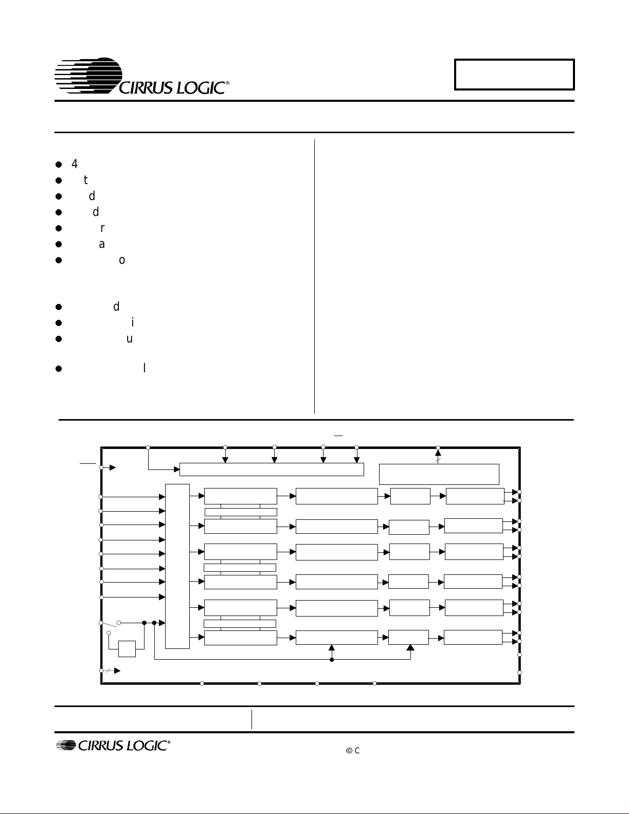
The C S4362 is a com plete 6-channel digital-to-analog
system including digital i nterpolation, fifth-order deltasigma digital-to-analog conversion, digital de-em phas is,
volume control and analog filtering. The advant ages of
this architecture include: ideal differential linearity, no
distortion mechanism s due to res istor matching errors,
no linearity drift over time and temperature and a hi gh
tolerance to clock jitter.
The CS4362 accepts PCM data at sample rates from
4 k Hz to 192 kHz, DSD audio data, and operates over a
wide power supply range. These features are ideal for
multi-channel audio systems including D VD players.
SACD players, A/V receivers, digital T V’s and VCR’s,
mixing consoles, effects process ors and s et-top box
systems.
ORDERING INFORM ATION
CS4362-KQ -10 to 70 48-pin LQ FP
CS4362-BQ -40 to 85 48-pin LQ FP
CDB4362 Evaluation Board
MUTEC [1:6]
RST
VLS
SCLK
LRCK
SCLK
L RCK 2
SD I N1
SD IN2
SD IN3
MCLK
DSDxx
1
1
2
2
÷
6
Volume C ontrol Interpolation Filter Analog Filter∆Σ
Mixer
Volume C ontrol
Volume C ontrol Interpolation Filter A nalog Filter∆Σ
Mixer
S e ri al P o rt
Volum e C ontrol
Volume C ontrol Interpolation Filter A nalog Filter∆Σ
Mixer
Volum e C ontrol
Preliminary Product Information
P.O. Box 17847, Austin, Texas 78760
(512) 445 7222 FAX: (512) 445 7581
http://www.cirrus.com
6
Control P ort/Mode Select
Interp olation Filter
Interp olation Filter
Interp olation Filter
GND
VAGNDVD
Mute Control
DAC
∆Σ
DAC
DAC
∆Σ
DAC
DAC
∆Σ
DAC
External
Analog Filter
Analog Filter
Analog Filter
This document contains information for a new product.
Cirrus Logic reserves the right to modify this product withoutnotice.
CopyrightCirrus Logic, Inc. 2002
(All Rights Reserved)
AO UTA1+
AO UTA1-
AO UTB1+
AO UTB1-
AO UTA2+
AO UTA2-
AO UTB2+
AO UTB2-
AO UTA3+
AO UTA3-
AO UTB3+
AO UTB3-
VQ
FILT+
MAR ‘02
DS257PP2
1
TABLE OF CONTENTS
1. CHARACT ERISTICS AND SPECIFICATIONS ........................................................................4
2. REGISTER Q UICK REFERENCE ..........................................................................................14
3. REGISTER DESCRIPTION ....................................................................................................15
4. PIN DESCRIPTION .................................................................................................................24
5. APPLICATIONS ...................................................................................................................... 27
5.1 G rounding and Power Supply Decoupling .......................................................................27
5.2 Oversampling Modes .......................................................................................................27
5.3 Recommended P ower-up S equenc e ...............................................................................27
5.4 Analog Output and Filtering .............................................................................................27
5.5 Interpolation Filter ............................................................................................................27
5.6 Clock Source Selection ....................................................................................................28
5.7 Using DSD mode .............................................................................................................28
6. CONTROL PORT INTERFACE.............................................................................................. 28
6.1 Enabl ing the Control Port .................................................................................................28
6.2 Format Selection ..............................................................................................................28
2
6.3 I
C Format .......................................................................................................................29
6.3.1 Writing in I
6.3.2 Reading in I
6.4 SPI Format .......................................................................................................................29
6.4.1 Writing in SPI ......................................................................................................29
6.5 Memory A ddress Pointer (MAP)......................................................................................30
7. PARAMETER DEFINITIONS.................................................................................................. 38
8. REFERENCES ........................................................................................................................ 38
9. PACKAGE DIMENSIONS .......................................................................................................39
CS4362
2
C Format ...........................................................................................29
2
C Format ........................................................................................29
LIST OF FIGURES
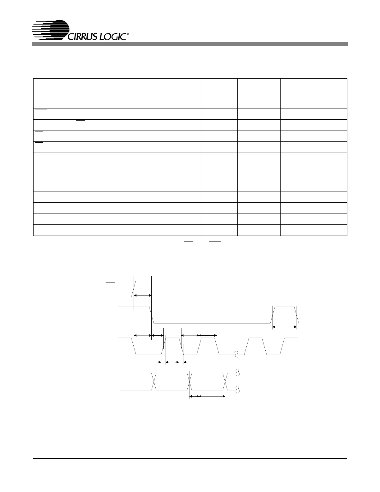
Figure 1 . Serial Mode Input Timing .................................................................................................8
Figure 2 . Direct Stream Digital - Serial Audio Input Timing .............................................................9
Figure 3. Control Port Timing - I
Contacting Cirrus Logic Support
For a complete listing of Direct Sales, Distributor, and Sales Representative contacts, visit the Cirrus Logic web site at:
http://www.cirrus.com/corporate/contacts
IMPORTANT NOTICE
"Preliminary" product information describes products that are in production, but for which full characterization data is not yet available. "Advance" product informa-
tion describes products that are in development and subject to development changes. Cirrus Logic, Inc. and its subsidiaries ("Cirrus") believe that the information
contained in this document is accurate and reliable. However, the information is subject to change without notice and is provided "AS IS" without warranty of any
kind (express or implied). Customers are advised to obtain the latest version of relevant information to verify, before placing orders, that information being relied
onis current and complete. All products aresoldsubject to thetermsand conditions of salesupplied at the time of order acknowledgment, including thosepertaining
to warranty, patent infringement, and limitation of liability. No responsibility is assumed by Cirrus for the use of this information, including use of thisinformatio nas
the basis for manufacture or sale of any items, or for infringement of patents or other rights of third parties. This document isthe property of Cirrus and by furnishing
this information, Cirrus grants no license, express or impliedunder any patents, mask workrights, copyrights, trademarks,trade secretsor other intellectual property
rights. Cirrus owns the copyrights of the information containedherein and gives consent forcopies to be made of the information only for use withinyour organization
with respect to Cirrus integrated circuits or other parts of Cirrus. This consent does not extend to other copyingsuch as copying for general distribution,advertising
or promotional purposes, or for creating any work for resale.
An export permit needs to be obtained fromthe competent authorities of the Japanese Government if any of the products or technologies described in this material
and controlled under the"Foreign Exchange and Foreign Trade Law" is to be exportedor taken out of Japan. A nexport license and/or quota needs to be obtained
from the competent authorities of theChineseGovernment if any of the products or technologies described in this material is subject to the PRC Foreign Trade Law
and is to be exported or taken out of the PRC.
CERTAIN APPLICATIONS USING SEMICONDUCTOR PRODUCTS MAY INVOLVE POTENTIAL RISKS OF DEATH, PERSONAL INJURY, OR SEVERE PROPERTY OR ENVIRONMENTAL DAMAGE ("CRITICAL APPLICATIONS"). CIRRUS PRODUCTS ARE NOT DESIGNED, AUTHORIZED, OR WARRANTED TO BE
SUITABLE FOR USE IN LIFE-SUPPORT DEVICES OR SYSTEMS OR OTHER CRITICAL APPLICATIONS. INCLUSION OF CIRRUS PRODUCTS IN SUCH
APPLICATIONS IS UNDERSTOOD TO BE FULLY AT THE CUSTOMER'S RISK.
Purchase of I
those components in a standard I
Cirrus Logic, Cirrus, andthe Cirrus Logic logo designs are trademarks of Cirrus Logic, Inc. A ll other brand and product names inthis document may be trademarks
or service marks of their respective owners.
2
C components of Cirrus Logic, Inc., or one of its sublicensed Associated Companies conveys a license under the Phillips I2C Patent Rights to use
2
Csystem.
2
C Format ...................................................................................10
2

CS4362
Figure 4 . Control Port Timing - SPI Format................................................................................... 11
Figure 5 . Typical Connection Diagram Control Port......................................................................12
Figure 6 . Typical Connection Diagram Stand-Alone..................................................................... 13
Figure 7. Control Port Timing, I
Figure 8 . Control Port Timing, SPI Format.................................................................................... 30
Figure 9 . Single Speed (fast) Stopband Rejection........................................................................ 31
Figure 1 0. Single Speed (fast) Transition Band ............................................................................ 31
Figure 1 1. Single Speed (fast) Transition Band (detail) . . ..............................................................31
Figure 1 2. Single Speed (fast) Passband Ripple .......................................................................... 31
Figure 13. Single Speed (slow) Stopband Rejection..................................................................... 31
Figure 14. Single Speed (slow) Transition Band........................................................................... 31
Figure 1 5. Single Speed (slow) Transition Band (detail)............................................................... 32
Figure 16. Single Speed (slow) Passband Ripple......................................................................... 32
Figure 1 7. Double Spee d (fast) Stopband Rejection ..................................................................... 32
Figure 1 8. Double Spee d (fast) Transition Band........................................................................... 32
Figure 1 9. Double Spee d (fast) Transition Band (detail)............................................................... 32
Figure 2 0. Double Spee d (fast) Passband Ripple......................................................................... 32
Figure 2 1. Double Speed (slow) Stopband Rejection ................................................................... 33
Figure 2 2. Double Speed (slow) Transition Band .........................................................................33
Figure 2 3. Double Speed (slow) Transition Band (detail) .............................................................33
Figure 2 4. Double Speed (slow) Passband Ripple ....................................................................... 33
Figure 2 5. Quad Speed (fast) Stopband Rejection.......................................................................33
Figure 2 6. Quad Speed (fast) Transition Band .............................................................................33
Figure 2 7. Quad Speed (fast) Transition Band (detail)................................................................. 34
Figure 2 8. Quad Speed (fast) Passband Ripple ........................................................................... 34
Figure 2 9. Quad Speed (slow) Stopband Rejection...................................................................... 34
Figure 3 0. Quad Speed (slow) Transition Band............................................................................34
Figure 3 1. Quad Speed (slow) Transition Band (detail)................................................................ 34
Figure 3 2. Quad Speed (slow) Passband Ripple.......................................................................... 34
Figure 3 3. Format 0 - Left Justified up to 24-bit Data.................................................................... 35
Figure 34. Format1 - I
Figure 3 5. Format 2 - R ight Justified 16-bit Data .......................................................................... 35
Figure 3 6. Format 3 - R ight Justified 24-bit Data .......................................................................... 35
Figure 3 7. Format 4 - R ight Justified 20-bit Data .......................................................................... 36
Figure 3 8. Format 5 - R ight Justified 18-bit Data .......................................................................... 36
Figure 3 9. De-Emphasis Curve.....................................................................................................36
Figure 4 0. Chann el Pair Routing Diagram (x = C hannel Pair 1, 2, or 3)....................................... 36
Figure 4 1. ATAPI Block Diagram (x = channel pair 1, 2, or 3)...................................................... 37
Figure 4 2. Recommended Output Filter........................................................................................37
2
S up to 24-bit Data...................................................................................35
2
C Format .................................................................................... 30
LIST OF TABLES
Table 1. Digital Interface Formats - PCM Mode............................................................................ 16
Table 2. Digital Interface Formats - DSD Mode............................................................................16
Table 3. ATAPI Decode ................................................................................................................ 21
Table 4. Example Digital Volume Settings .................................................................................... 22
Table 5. Commo n Clock Frequenc ies........................................................................................... 26
Table 6. Digital Interface Format, Stand-Alone M ode Options...................................................... 26
Table 7. Mode Selection, Stand-Alone Mode O ptions.................................................................. 26
Table 8. Direct Stream Digital (DSD), Stand-Alone Mode Options...............................................26
3
CS4362
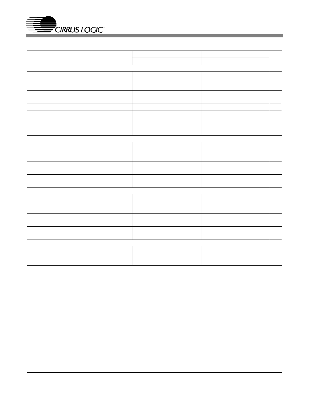
1. CHARACTERISTICS AND SPECIFICATIONS
ANALOG CHARACTERISTICS (Full-Scale Output Sine Wave, 997 Hz; Measuremen t Bandwid th
10 Hz to 20 kHz, unless otherwise specified; Test load R
For Single speed Mode Fs = 48 kHz, SCLK = 3.072 MHz, MCLK = 12.288 MHz;
For Double Speed Mode Fs = 96 kHz, SCLK = 6.144 MHz, MCLK = 12.288 MHz;
For Quad Speed Mode Fs = 192 kHz, SCLK = 12.288 MHz, MCLK = 24.576 MHz;
For Direct Stream Digital Mode Fs = 128 x 48 kHz, DSD_SCLK = 6.144 MHz , MCLK = 12.288 MHz).
Parameters Symbol Min Typ Max Unit
CS4362-KQ Dynamic Performance - All PCM mo des and DSD (Note 1)
Specified Temperature Range T
Dynamic Range (Note 2) 24-bit unweighted
A-Weighted
16-bit unweighted
(Note 3) A-Weighted
Total Harmonic Distortion + Noise (Note 2 )
24-bit 0 dB
-20 dB
-60 dB
16-bit 0 dB
(Note 3) -20 dB
-60 dB
Idle Channel Noise / Signal-to-noise ratio - 114 - dB
Interchannel Isolation (1 k Hz ) - 90 - dB
CS4362-BQ Dynamic Performance - All PCM mo des and DSD (Note 4)
Specified Temperature Range T
Dynamic Range (Note 2) 24-bit unweighted
A-Weighted
16-bit unweighted
(Note 3) A-Weighted
Total Harmonic Distortion + Noise (Note 2 )
24-bit 0 dB
-20 dB
-60 dB
16-bit 0 dB
(Note 3) -20 dB
-60 dB
Idle Channel Noise / Signal-to-noise ratio - 114 - dB
Interchannel Isolation (1 k Hz ) - 90 - dB
=3kΩ,CL= 100 pF, VA = 5 V, VD = 3.3V (see Figure 5)
L
A
THD+N
A
THD+N
-10 - 70 °C
105
108
-
-
-
-
-
-
-
-
-40 - 85 °C
102
105
-
-
-
-
-
-
-
-
111
114
94
97
-100
-91
-51
-94
-74
-34
111
114
94
97
-100
-91
-51
-94
-74
-34
-
-
-
-
-94
-
-
-
-
-
-
-
-
-
-91
-
-
-
-
-
dB
dB
dB
dB
dB
dB
dB
dB
dB
dB
dB
dB
dB
dB
dB
dB
dB
dB
dB
dB
Notes: 1. CS4362-KQ parts are tested at 25 °C.
2. One-half LSB of triangular PDF dither is added to data.
3. Performance limited by 16-bitquantization noise.
4. CS4362-BQ parts are tested at the extremes of the specifiedtemperature range and Min/Max
performance numbers are guaranteed across the specified temperature range, T
takenat25°C.
4
. Typical numbers are
A
CS4362
ANALOG CHARACTERISTICS (Continued)
Parameters Symbol Min Typ Max Units
Analog Output - All PCM mo des an d DSD
FullScaleDifferential OutputVoltage (Note 5) V
Quiescent Voltage V
Max Currentfrom V
Q
FS
I
QMAX
Q
Interchannel Gain Mismatch - 0.1 - dB
Gain Drift - 100 - ppm/°C
Output Impedance (Note 5) Z
AC-Load Resistance R
Load C apacitance C
OUT
L
L
POWER AND THERMAL CHARACTERISTICS
Parameters Symbol Min Typ Max Units
Power Supplies
Power Supply Current normal operation, V
(Note 6) V
Interface current, VLC=5V (Note 7, 8)
power-down state (all supplies) (Note 9)
Power Dissipation (Note 6)
VA = 5 V, VD = 3.3 V normal operation
power-down (Not e 9)
VA = 5 V, VD = 5 V normal operation
power-down (Not e 9)
Package Thermal Resistance θ
Power Supply Rejection Ratio (Note 10) (1 k Hz )
A
D
V
=3.3V
D
VLS=5V
(60 Hz)
=5V
=5V
88% V
A
92% V
A
94% V
A
Vpp
-50%VA-VDC
-1 -µA
- 100 - Ω
3- -kΩ
- - 100 pF
I
A
I
D
I
D
I
LC
I
LS
I
pd
JA
θ
JC
PSRR -
-
-
-
-
-
-
-
-
-
-
-
-
50
38
25
2
84
200
335
1
440
1
48
15
60
-
40
55
60
40
-
-
-
410
-
575
-
-
-
-
-
mA
mA
mA
µA
µA
µA
mW
mW
mW
mW
°C/Watt
°C/Watt
dB
dB
Notes: 5. VFSis tested under load RLand includes attenuation due to Z
6. Current cons umption increases with increasing FS within a given s peed mode and is signal dependant.
Max values are based on highest FS and highest MCLK.
7. I
measured wi th no external loading on the SDA pin.
LC
8. This s pec ification is violated when the VLC s upply is greater than VD and when pin 16 (M1/SDA) i s t ied
or pulled low. Logic tied to pin 16 needs to be able to sink this current .
9. Power down mode is defined as RST
pin = L ow w ith all clock and data lines held static.
10. Valid with the recommended capac itor values on FILT+ and VQ as shown in Figures 5 and 6.
OUT
5
CS4362
ANALOG FILTER RESPONSE
Fast Roll-Off Slow Roll-Off (Note 11)
Parameter
Combined Digital and On-chip Analog Filter Response - Single Speed Mode (Note 12)
Passband (Note 13) to -0.01 dB corner
to -3 dB corner00
Frequency Response 10 Hz to 20 k Hz -0.01 - +0.01 -0.01 - +0.01 dB
StopBand .547 - - .583 - - Fs
StopBand Attenuation (Note 14) 90 - - 64 - - dB
Group Delay - 12/Fs - - 6.5/Fs - s
Passband Group Delay Deviation 0 - 20 kHz - - ±0.41/Fs - ±0.14/Fs s
De-emphasis Error (Note 1 5) Fs = 32 k H z
(Relative to 1kHz) Fs = 44.1 kHz
Fs = 48 kHz
Combined Digital an d On -chip Analog Filter Response - Double Speed Mode - 96kHz (Note 12)
Passband (Note 13) to -0.01 dB corner
to -3 dB corner00
Frequency Response 10 Hz to 20 kHz -0.01 - 0.01 -0.01 - 0.0 1 dB
StopBand .583 - - .792 - - Fs
StopBand Attenuation (Note 14) 80 - - 70 - - dB
Group Delay - 4.6/Fs - - 3.9/Fs - s
Passband Group Delay Deviation 0 - 20 kHz - - ±0.03/Fs - ±0.01/Fs s
Combined Digital and On-chip Analog Filter Respons e - Quad Speed Mode - 192kHz (Note 12)
Passband (Note 13) to -0.01 dB corner
to -3 dB corner00
Frequency Response 10 Hz to 20 kHz -0.01 - 0.01 -0.01 - 0.0 1 dB
StopBand .635 - - .868 - - Fs
StopBand Attenuation (Note 14) 90 - - 75 - - dB
Group Delay - 4.7/Fs - - 4.2/Fs - s
Passband Group Delay Deviation 0 - 20 kHz - - ±0.01/Fs - ±0.01/Fs s
Combined Digital and On-chip Analog Filter Response - DSD Mode (Note 12)
Passband (Note 13) to -0.1 dB c orner
to -3 dB corner
Frequency Response 10 Hz to 20 kHz - - - -.01 - 0.1 dB
Notes: 11. Slow Roll-Offinterpolation filter is only availablein control port mode.
12. Filter response is not tested but is guaranteedby design.
13. Response is clock dependent and will scale with Fs. Note that the response plots (Figures 9 to 32) have
been normalized to Fs and can be de-normalized by multiplying the X-axis scale by Fs.
14. Single and Double Speed Mode Measurem ent Bandwidth is from stopband to 3 Fs.
Quad Speed Mode Measurement Bandwidth is from stopband to 1.34 Fs.
15. De-emphasis is available only in Single Speed Mode; Only 44.1kHz De-emphasis is av ailable in StandAlone Mode
-
-
-
-
-
-
-
-
-
-
-
-
-
-
-
-
.454
.499
±0.23
±0.14
±0.09
.430
.499
.105
.490
-
-
0
0
-
-
-
0
0
0
0
0
0
-
-
-
-
-
-
-
-
-
-
-
0.417
0.499
±0.23
±0.14
±0.09
.296
.499
.104
.481
20
120
UnitMin Typ Max Min Typ Max
kHz
kHz
Fs
Fs
dB
dB
dB
Fs
Fs
Fs
Fs
6

CS4362
DIGITAL CHAR ACTERISTICS (For KQ T
=-10to+70°C;ForBQTA=-40to+85°C;VLC=VLS=
A
1.8 V to 5.5 V)
Parameters Symbol Min Typ Max Units
High-Level Input Voltage Serial Data Port
Control P ort
Low-Level Input Voltage Serial Data Port
Control P ort
Input Leakage Current (Note 8) I
V
V
V
V
IH
IH
IL
IL
in
70% VLS
70% VLC
-
-
-
-
-
20% VLS
-
20% VLCVV
-
-
--±10µA
V
V
Input Capacitance - 8 - pF
Maximum MUTEC Drive C urrent - 3 - mA
MUTEC High-Level Output Voltage V
MUTEC Low-Level Output Voltage V
OH
OL
-VA-V
-0-V
ABSOLUTE MAXIMUM RATINGS (GND = 0V; all voltages wi th respect to ground.)
Parameters Symbol Min Max U nits
DC Power Supply Analog power
Digital internal power
Serial dataport interface power
Control port interface power
Input Current, Any Pin Except Supplies I
Digital InputVoltage Serial dataport interface
Control port interface
Ambient Operating Temperature (power applied) T
Storage Tem perature T
WARNING: Operation at or beyond these limits may result in permanent damage to the device. Normal operation is
not gu aranteed at these extremes.
VD
VLS
VLC
V
IND-S
V
IND-C
VA
stg
-0.3
-0.3
-0.3
-0.3
in
-±10mA
-0.3
-0.3
A
-55 125 °C
6.0
6.0
6.0
6.0
VLS+ 0.4
VLC+ 0.4
V
V
V
V
V
V
-65 150 °C
RECOMMENDED OPERATING CONDITIONS (GND = 0V; all voltages with respect to ground.)
Parameters Symbol Min Typ Max Units
DC Power Supply Analog powe r
Digital internal power
Serial dataport interface power
Control port interface power
VA
VD
VLS
VLC
4.5
3.0
1.8
1.8
5.0
3.3
5.0
5.0
5.5
5.5
5.5
5.5
V
V
V
V
7
CS4362
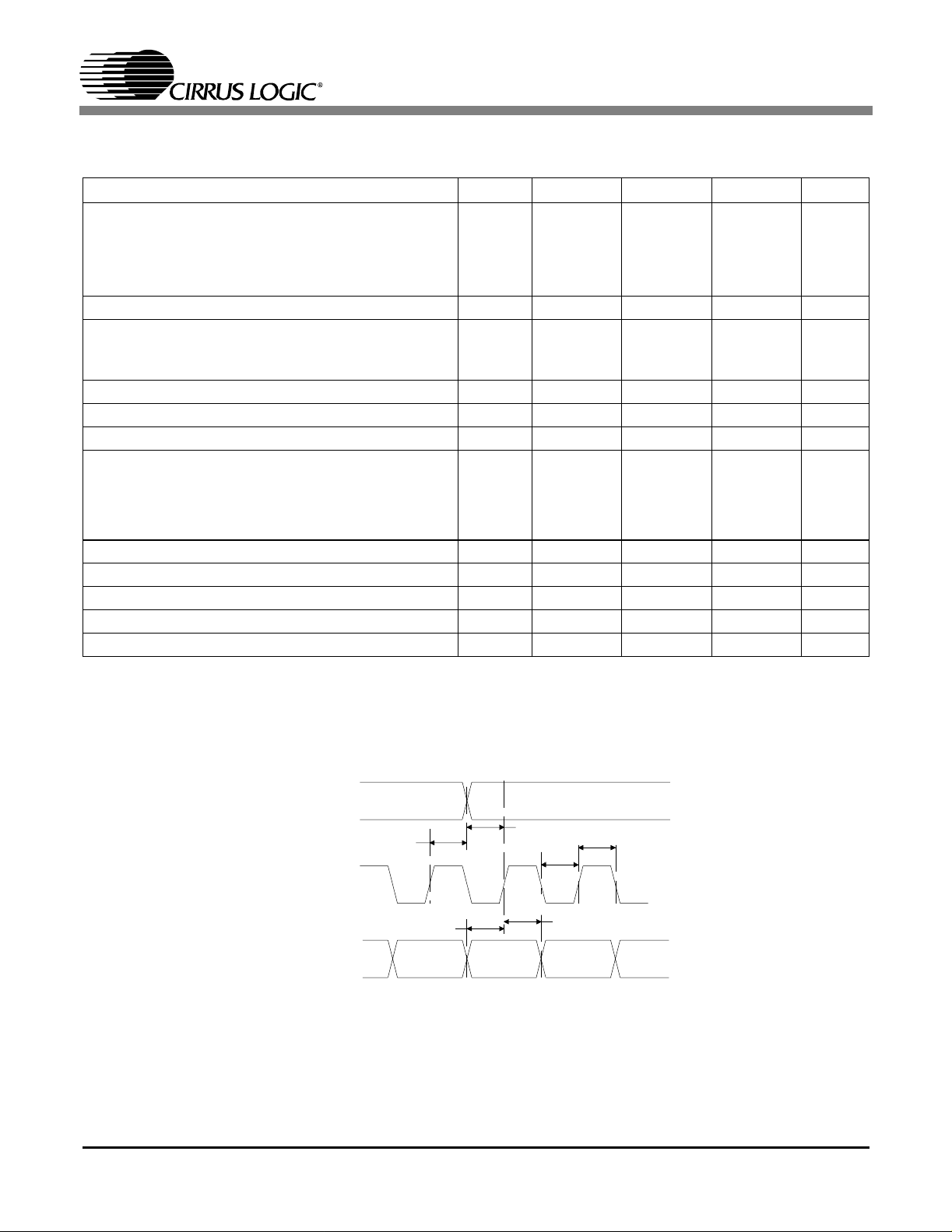
SWITCHING CHARACTERISTI CS (For KQ T
1.8 V to 5.5 V; Inputs: Logic 0 = GND, Logic 1 = VLS, C
=-10to+70°C;ForBQTA=-40to+85°C;VLS=
A
= 30pF)
L
Parameters Symbol Min Typ Max Units
MCLK Frequency (Note 16)
Single Speed Mode 1.024 - 51.2 MHz
Double Speed Mode 6.400 - 51.2 MHz
Quad Speed Mode 6.400 - 51.2 MHz
MCLK Duty Cycle 40 50 60 %
Input S ample Rate Single Speed Mode
Double Speed Mode
Quad Speed Mode
Fs
Fs
Fs
4
50
100
-
-
-
50
100
200
kHz
kHz
kHz
LRCK Duty Cycle 45 50 55 %
SCLK Pulse Wi dth Low t
SCLK Pulse Width High t
SCLK Period t
(Note 17) t
SCLK rising to LRCK edge delay t
SCLK rising to LRCK edge setup time t
SDATA valid to SCLK rising setup time t
SCLK rising to SDATA hold time t
sclkl
sclkh
sclkw
sclkw
slrd
slrs
sdlrs
sdh
20 - - ns
20 - - ns
2
------------------
MCLK
4
------------------
MCLK
--ns
--ns
20 - - ns
20 - - ns
20 - - ns
20 - - ns
LRCK1 to LRCK2 frequenc y ratio (Note 18) 0.25 1.00 4.00
Notes: 16. See T able 5 on page 26 for suggested MCLK frequencies
17. This serial clock is available only in Cont rol Port Mode when the MCLK Divide bit is enabled.
18. The higher frequency LRCK mus t be an exact integer mul tiple (1, 2, or 4) of the lower frequency LRCK
.
LRCK
t
t
slrd
SCLK
t
sdlrs
SDATA
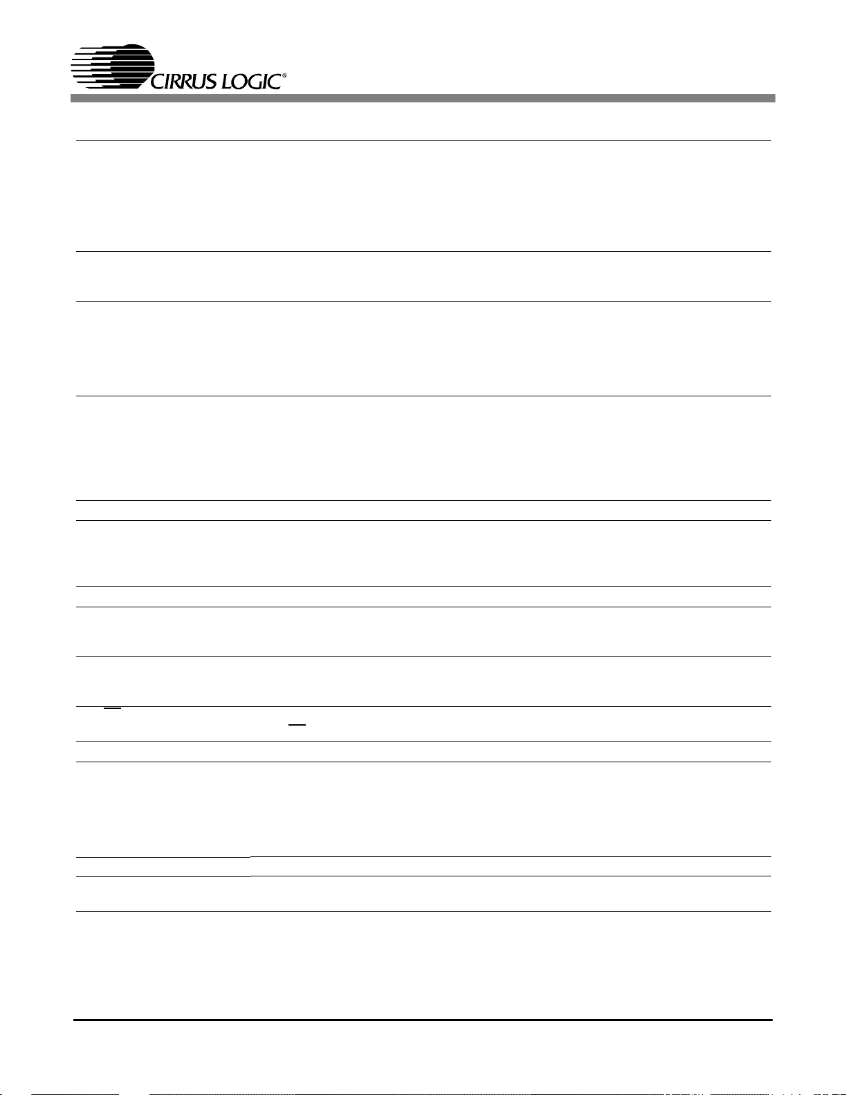
Figure 1. Serial Mode Input Timing
slrs
t
sclkl
t
sdh
t
sclkh
8
CS4362
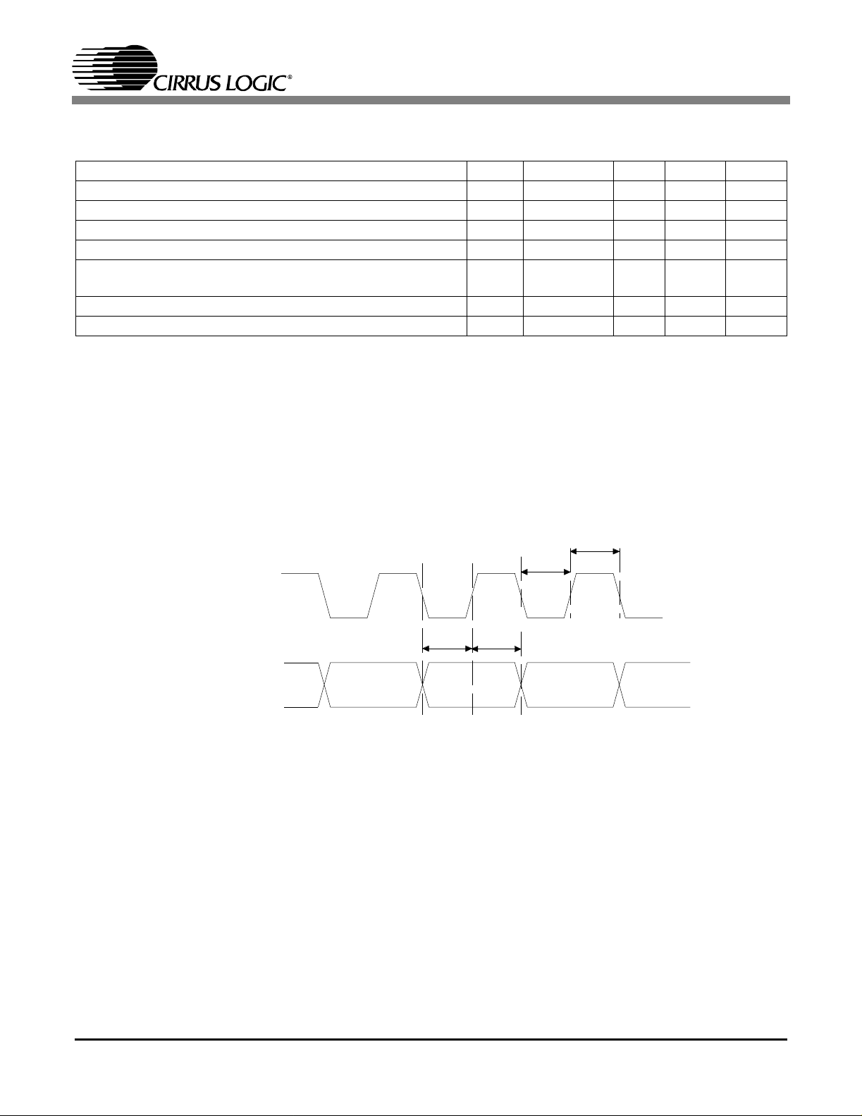
DSD - SWITCHING CHARACTERISTICS (T
5.5 V; Logic 1 = VLS Volts; C
=30pF)
L
= -10 t o 70°C; Logic 0 = GND; VLS = 1.8 V to
A
Parameter Symbol Min Typ Max Unit
Master Clock Frequency (Note 19) 4.096 - 38.4 MHz
MCLK Duty Cycle (All DSD modes) 40 50 60 %
DSD_SCLK Pulse Width Low t
DSD_SCLK Pulse W idth High t
DSD_SCLK Frequency (64x Oversam pled)
(128x Oversampled)
DSD_L / _R valid to DSD_SCLK rising setup time t
DSD_SCLK rising to DSD_L or DSD_R hold time t
sclkl
sclkh
sdlrs
sdh
20 --ns
20 --ns
1.024
2.048
-
-
3.2
6.4
MHz
MHz
20 --ns
20 --ns
Note: 19. Min is 4 times 64x DSD or 2 times 128x DSD, and Max is 12 times 64x DSD or 6 times 128x DSD. The
proper MCLK to DSD_SCLK ratio must be set either by the DIF registers or the M0:2 pins
t
sclkh
t
sclkl
DSD_SCLK
DSD_L, DSD_R
Figure 2. Direct Stre am Digital - Serial Audio Input Timing
sdlrstsdh
t
9
CS4362
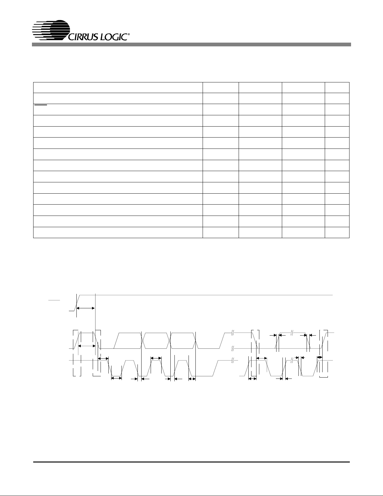
SWITCHING CHARACTERISTICS - CONTROL PORT - I2CFORMAT
(For KQ TA=-10to+70°C; For BQ TA=-40to+85°C; VLC = 1.8 V to 5.5 V; Inputs: Logic 0 = GND, Logic
1=VLC,C
SCL Clock Frequency f
Rising Edge to Start t
RST
Bus F ree Time Between Transmissions t
Start C ondition Hold Time (prior to first clock pulse) t
Clock Low time t
Clock High Time t
Setup Time for Repeated Start Condition t
SDA Hold Time from SCL Falling (Note 20) t
SDA Setup time to SCL Rising t
Rise Time of SCL and SDA t
Fall TimeSCL and SDA t
Setup Time for Stop Condition t
Acknowledge Delay from SCL Falling (Note 21 ) t
=30pF)
L
Parameter Symbol Min Max Unit
scl
irs
buf
hdst
low
high
sust
hdd
sud
rc,trc
fc,tfc
susp
ack
- 100 kHz
500 - ns
4.7 - µs
4.0 - µs
4.7 - µs
4.0 - µs
4.7 - µs
0-µs
250 - ns
-1µs
- 300 ns
4.7 - µs
-(Note22)ns
Notes: 20. Data must be held for s ufficient time to bridge the transition t im e, t
21. The acknowledge delay is based on MCLK and can limit the maximum transaction speed.
15
22. forSingle-Speed Mode, forDouble-Speed Mode, forQuad-SpeedMode.
RST
SDA
SCL
--------------------256 Fs×
t
irs
Stop S t a rt
t
buf
t
hdst
t
low
t
hdd
t
high
15
-------------------- 128 Fs×
t
sud
t
Repeated
ack
Figure 3. Control Port Timing - I2CFormat
,ofSCL.
fc
Start
t
sust
15
----------------- 64 Fs×
t
rd
t
hdst
Stop
t
fd
t
fc
t
rc
t
susp
10
CS4362
SWITCHING CHARACTERISTI CS - CONTROL PORT - SPI FORMAT
(For KQ TA=-10to+70°C; For BQ TA=-40to+85°C; VLC = 1.8 V to 5.5 V; Inputs: Logic 0 = GND, Logic
1=VLC,C
CCLK Clock Fr equency f
RST
Rising Edge to CS Falling t
CCLK Edge to CS
High Time Between Transmissions t
CS
Falling to CCLK Edge t
CS
CCLK Low Time t
=30pF)
L
Parameter Symbol Min Max Unit
Falling (Note 23) t
sclk
srs
spi
csh
css
scl
-MHz
500 - ns
500 - ns
1.0 - µs
20 - ns
1
----------------- MCLK
MCLK
----------------- 2
-ns
CCLK High Time t
CDIN to CCLK Rising Setup Time t
CCLK Rising to DATA Hold Time (Note 24) t
Rise Time of CCLK and CDIN (Note 25) t
Fall Time of CCLK and CDIN (Note 25) t
Notes: 23. t
only needed before first falling edge of CS after RST rising edge. t
spi
24. Data must be held for sufficient t im e to bridge the transition time of CCLK .
25. For F
SCK
<1MHz.
RST
t
srs
CS
t
t
spi
css
t
scl
t
sch
CCLK
sch
dsu
dh
r2
f2
1
----------------- MCLK
-ns
40 - ns
15 - ns
- 100 ns
- 100 ns
= 0 at all other times.
spi
t
csh
CDIN
t
r2
t
t
f2
dsu
t
dh
Figure 4. Control Port Timing - SPI Format
11
CS4362
+3.3 V to + 5 V
+1.8Vto+5V
Micro-
Co ntroller
PCM
Digital
Audio
Source
DSD
Audio
Source
1µF
0.1 µ F
10
12
11
13
43
47
46
42
19
15
16
17
+
6
7
9
8
3
2
1
48
0.1 µF
VD
MCLK
LRCK 1
SCLK1
LRCK2
SCLK2
SDIN1
SDIN2
SDIN3
VLS
DSDA1
DSDB1
DSDA2
DSDB2
DSDA3
DSDB3
DSD_SCLK
RST
SCL/CC LK
SDA/CDIN
ADO/CS
4
CS4362
32
VA
AOUTA1+
AOUTA1-
AOUTB1+
AOUTB1-
AOUTA2+
AOUTA2-
AOUTB2+
AOUTB2-
AOUTA3+
AOUTA3-
AOUTB3+
AOUTB3-
MUTEC1
MUTEC2
MUTEC3
MUTEC4
MUTEC5
MUTEC6
0.1 µ F
39
40
38
37
35
36
34
33
29
30
28
27
41
26
25
24
23
22
+
1µF
Analog Conditioning
and M uting
Analog Conditioning
and M uting
Analog Conditioning
and M uting
Analog Conditioning
and M uting
Analog Conditioning
and M uting
Analog Conditioning
and M uting
Mute
Drive
+5 V
+1.8 V to +5 V
12
Ω
2K
Note*:Necessary for I2C
control port o peration
Ω
2K
Note*
0.1 µF
Figure 5. Typical Connection Diagram Control Port
18
VLC
GND
5
GND
31
FILT+
CMOUT
20
21
0.1 µ
+
47 µF
F
F
1µF
+
0.1 µ

CS4362
+3.3Vto+5V
VLS
+1.8Vto+5V
Note
PCM
Digital
Audio
Source
Audio
Source
DSD
DSD
1µF
47 K
Ω
0.1 µF
Note
10
12
11
13
43
DSD
+
6
7
9
8
3
2
1
48
47
46
0.1 µF
MCLK
LRCK1
SCLK1
LRCK2
SCLK2
SDIN1
SDIN2
SDIN3
VLS
DSDA1
DSDB1
DSDA2
DSDB2
DSDA3
DSDB3
4
VD
CS4362
32
VA
AOUTA1+
AOUTA1-
MUTEC1
AOUTB1+
AOUTB1-
MUTEC2
AOUTA2+
AOUTA2-
MUTEC3
AOUTB2+
AOUTB2-
MUTEC4
AOUTA3+
AOUTA3-
MUTEC5
0.1 µF
39
40
41
38
37
26
35
36
25
34
33
24
29
30
23
+
1µF
Analog C onditioning
and Muting
Analog C onditioning
and Muting
Analog C onditioning
and Muting
Analog C onditioning
and Muting
Analog C onditioning
and Muting
+5 V
Stand-Alone
Mode
Configuration
+1.8Vto+5V
VLC
Note
:Ifseriesresistorsare
used they m ust be <1k O hm. If
possible tie VLC to the VD supply
to reduce possible excess current
consum ption from VLC .
47 K
Ω
42
Note
VLC
0.1 µF
M3(DSD_SCLK)
15
M2
16
M1
17
M0
19
RST
18
VLC
GND
5
AOUTB3+
AOUTB3-
MUTEC6
CMOUT
GND
31
FILT+
28
27
22
20
21
Figure 6. Typical Connection Diagram Stand-Alone
Analog C onditioning
and Muting
+
47 µF
F
F
0.1 µ
DSD
Note
1)LRCK1mustbetiedtoVLSand
rema in st a t ic high.
2) M 3 PCM stand-alone configuration
pin becom es DSD_SCLK
1µF
+
: For DSD operation:
0.1 µ
13

CS4362
2. REGISTER QUICK REFERENCE
Addr Function 7 6 5 4 3 2 1 0
01h Mode Control 1 CPEN FREEZE
default
02h Mode Control 2 Reserved DIF2 DIF1 DIF0 Reserved SDIN3CLK SDIN2CLK SDIN1CLK
default
03h Mode Control 3 SZC1 SZC0 SNGLVOL RMP_UP MUTEC+/- AMUTE MUTEC1 MUTEC0
default
04h Filter Control Reserved Reserved Reserved FILT_SEL Reserved DEM1 DEM0 RMP_DN
default
05h Invert Control Reserved Reserved INV_B3 INV_A3 INV_B2 INV_A2 I NV_B1 I NV_A1
default
06h Mixing Control
Pair 1 (AOUTx1)
default
07h Vol.Control A1 A1_MUTE A1_VOL6 A1_VOL5 A1_VOL4 A1_VOL3 A1_VOL2 A1_VOL1 A1_VOL0
default
08h Vol.Control B1 B1_MUTE B1_VOL6 B1_VOL5 B1_VOL4 B1_VOL3 B1_VOL2 B1_VOL1 B1_VOL0
default
09h Mixing Control
Pair 2 (AOUTx2)
default
0Ah Vol. Control A2 A2_MUTE A2_VOL6 A2_VOL5 A2_VOL4 A2_VOL3 A2_VOL2 A2_VOL1 A2_VOL0
default
0Bh Vol. Control B2 B2_MUTE B2_VOL6 B2_VOL5 B2_VOL4 B2_VOL3 B2_VOL2 B2_VOL1 B2_VOL0
default
0Ch Mixing Control
Pair 3 (AOUTx3)
default
0Dh Vol.Control A3 A3_MUTE A3_VOL6 A3_VOL5 A3_VOL4 A3_VOL3 A3_VOL2 A3_VOL1 A3_VOL0
default
0Eh Vol. Control B3 B3_MUTE B3_VOL6 B3_VOL5 B3_VOL4 B3_VOL3 B3_VOL2 B3_VOL1 B3_VOL0
default
12h Chip Revision PART3 PART2 PART1 PART0 Reserved Reserved Reserved Reserved
default
00
00000000
10000100
00000000
00000000
P1_A=B P1ATAPI4 P1ATAPI3 P1ATAPI2 P1ATAPI1 P1ATAPI0 P1FM1 P1FM0
00100100
00000000
00000000
P2_A=B P2ATAPI4 P2ATAPI3 P2ATAPI2 P2ATAPI1 P2ATAPI0 P2FM1 P2FM0
00100100
00000000
00000000
P3_A=B P3ATAPI4 P3ATAPI3 P3ATAPI2 P3ATAPI1 P3ATAPI0 P3FM1 P3FM0
00100100
00000000
00000000
1110----
MCLKDIV
0
Reserved DAC3_DIS DAC2_DIS DAC1_DIS PDN
00001
14

CS4362
3. REGISTER DESCRIPTION
Note: All registers are read/write in I2C mode and write only in S PI, unless otherwise noted.
3.1 Mode Control 1 (address 01h)
76543210
CPEN FREEZE
00
MCLKDIV
0
3.1.1 CONTROL PORT ENABLE (CPEN)
Default = 0
0 - Disabled
1-Enabled
Reserved DAC3_DIS DAC2_DIS DAC1_DIS PDN
00001
Function
:
This bit defaults to 0, allowing the device to power-up in Stand-Alone mo de. The Control port mode
can be accessed by setting this bit to 1. This will allow the operation of the device to be controlle d by
the registers and the pin definitions will conform t o Control Port Mode. To ac c omplish a clean powerup, the user should write this bit within 10 ms following the release of Reset.
3.1.2 FREEZE CONTROLS (FREEZE)
Default = 0
0 - Disabled
1-Enabled
Function:
This func tion allows modifications to be made to the registers w ithout the changes taking effect until
the FREEZE is di sa bled. To make multiple changes in the Control port registers take ef f ect simultaneously, enable the FREEZE Bit, make all register changes , then Disable the FREEZE bit.
3.1.3 MASTER CLOCK DIV IDE ENABLE (MCLKDIV)
Default = 0
0 - Disabled
1-Enabled
Function:
The M CLKDIV bit enables a circuit which divides the externally applied MCLK signal by 2 prior to all
other internal circuitry.
3.1.4 DAC PAIR DISABLE ( DACX_DIS)
Default = 0
0-Enabled
1 - Disabled
Function:
When enabled the respectiv e DAC channel pai rx (AOUTAx and AOUTBx) will remain in a reset state.
It is advised that changes to these bits be made while the power down bit is enabled to eliminate the
possibility of audible artifacts.
15

CS4362
3.1.5 POWER DOWN (PDN)
Default = 1
0 - Disabled
1-Enabled
Function:
The entire device will enter a low-power state when this funct ion is enabled, and the contents of the
control registers are retained in this mode. The p ower-down bit defaults to ‘enabled’ on power-up and
must be disabled before normal operation in Control Port mode can occur.
3.2 Mode Control 2 (address 02h)
76543210
Reserved DIF2 DIF1 DI F0 Reserved SDIN3CLK SDIN2CLK SDIN1CLK
00000000
3.2.1 DIGITAL INTERFACE FORMAT (DIF)
Default = 000 - Format 0 (Left Justified, up to 24-bit data)
Function:
These bits s elect the interface format for the serial audio input. The Functional Mode bits determine
whether PCM or DS D mode is selected.
PCM Mode: The required relationship b etwe en the Left/Rightclock, serial clock and s erialdata is defined
by the Di gital Interface Format and the options are detailed in Figures 33-38.
DIF2 DIF1 DIF0 DESCRIPTION Format FIGURE
000
001
010
011
100
101
110
111
Left Justified, up to 24-bit data
I2S, up to 24-bit data
Right J us tified, 16-bit data
Right J us tified, 24-bit data
Right J us tified, 20-bit data
Right J us tified, 18-bit data
Reserved
Reserved
033
134
235
336
437
538
Table1.DigitalInterfaceFormats-PCMMode
DSD Mode: The relationship between the oversampling ratio of the DSD audio data and the required
Master clock to DS D data rate is defined by the Digital I nterface Format pins.
DIF2 DIF1 DIFO DESCRIPTION
0 0 0 64x oversampled DSD data with a 4x MCLK to DSD data rate
0 0 1 64x oversampled DSD data with a 6x MCLK to DSD data rate
0 1 0 64x oversampled DSD data with a 8x MCLK to DSD data rate
0 1 1 64x oversampled DSD data with a 12x M CLK to DSD data rate
1 0 0 128x ov ersampled DSD data with a 2x MCLK to DSD data rate
1 0 1 128x ov ersampled DSD data with a 3x MCLK to DSD data rate
1 1 0 128x ov ersampled DSD data with a 4x MCLK to DSD data rate
1 1 1 128x ov ersampled DSD data with a 6x MCLK to DSD data rate
Table 2. Digital Interface Formats - DSD Mode
16

CS4362
3.2.2 SERIAL AUDIO DATA CLOCK SOURCE (SDINXCLK)
Default = 0
0 - SDINx clocked by SCLK1 and LRCK1
1 - SDINx clocked by SCLK2 and LRCK2
Function:
The SDINxCLK bit specifies which SCLK/LRCK input pair is used to clock in the data on the given
SDINx line. For more details see “Clock Source Selection” on page 28.
3.3 Mode Control 3 (address 03h)
76543210
SZC1 SZC0 SNGLVOL RMP_UP Reserved AMUTE MUTEC1 MUTEC0
10000100
3.3.1 SOFT RAMP AND ZERO CROSS CONTROL (SZC)
Default = 10
00 - Immediate Change
01 - Zero Cross
10 - Soft Ramp
11 - So ft Ramp on Zero Crossings
Function:
Immediate Change
When Immediate Change is selected all level changes will t ak e effect immediat ely in one step.
Zero Cross
Zero Cross Enable dictat es that signal level changes, either by attenuation changes or muting, will
occur on a sig nal zero crossing to minimize audible artifacts. The requested level change will occur
after a timeout period between 512 and 1024 sampl e periods (10.7 ms to 21.3 ms at 48 kHz sampl e
rate) if the signal does not encounter a zero crossing. The zero cross funct ion is independently monitored and im plemented for each channe l.
Soft Ramp
Soft Ramp allows level changes, both muting and attenuation, to be implemented by incrementally
ramping, in 1/8 dB steps, from the c urrent level to the new level at a rate of 1 dB per 8 left/right clock
periods.
Soft Ramp on Zero Crossing
Soft Ramp and Zero Cross Enable dictates that signal level changes, either by attenuation c hanges
or muting, will occur in 1/8 dB steps and be implemented on a signal zero crossing. The 1/8 dB level
change will occur after a time out period between 512 and 1024 sample periods (10.7 m s to 21.3 ms
at 48 kHz sample rate) if the signal does not enco unter a zero crossing. The zero cross funct ion is
independently monitored and implemented for each channel.
17

3.3.2 SINGLE VOLUME C ONTROL (SNGLVOL)
Default = 0
0 - Disabled
1-Enabled
Function:
The individual channel v olum e le ve ls are independent ly cont ro lled by their respective Volume Control
Bytes when this func tion is disabled. The volume on all channels is determined by the A 1 Channel
Volume Control Byte, and the other Volume Control Bytes are ignored when this function is enabled.
3.3.3 SOFT VOLUME RAMP -UP A FTER ERROR (RMP_UP)
Default = 0
0 - Disabled
1-Enabled
Function:
An un-mute will be performed after executing a filter mode change, af ter a LRCK/MCLK ratio change
or error, and after changing the Functional Mode. When this feature is enabled, this un-mute is ef fected, similar to attenuation changes, by the Soft an d Ze ro Cros s bits in the ModeControl 3 register.
When disabled, an immediate un-mute is performed in these instances.
CS4362
Note: For best results, it is recommended that this feature be used in conjunction with the RMP_DN
bit.
3.3.4 MUTEC POLARITY (MUTEC+/-)
Default = 0
0-ActiveHigh
1-ActiveLow
Function:
The active polarity of the MUTEC pin(s) is determined b y this register. When set to 0 (default) the
MUTEC pins are high when active. When set to 1 the MUTEC pin(s) are low when active.
Note: When the on board mute circuitry is des igned for active low, the MUTEC outputs will be high
(un-muted) for the period of time during reset and before this bit is enabled t o 1.
3.3.5 AUTO-MUTE (AMUTE)
Default = 1
0 - Disabled
1-Enabled
Function:
The Digital-to-Analog converter output will mute following the reception of 8192 consecutive audio
samples of s tatic 0 or -1. A s ingle sample of non-static data will release the mute. Detecti on and
muting is done independently for each channel. The quiescent voltage on the output will be retained
and the Mute Control pin will go active during t he mutepe riod. Themuting function is affected, sim ilar
to volume control changes, by the Soft and Zero Cross bits in t he Mod e Control 3 register.
18
CS4362
3.3.6 MUTE PIN CONTRO L(MUTEC1, MUTEC0)
Default = 00
00 - Six mute control signals
01 - Three mute control signals
10 - One m ute control signal
11 - Res erve d
Function:
Selects how the internal mute control signals are routed to the MUTEC1 through MUTEC6 pins.
When set to ‘00’, there is one m ut e control signal f or each channel: AOUT1A on MUTEC1, AOUT1B
on MUTEC2, etc. When set to ‘01’, there are three m ute control signals, one for each stereo pair:
AOUT1A and AOUT1B on MUTEC1, AOUT2A and AOUT2B on MUTEC2, and AOUT3A and
AOUT3B on MUTEC3. When set to ‘10’, there is a single mute control signal on the MUTEC1 pin.
3.4 Filter Control (address 04h)
76543210
Reserved Reserved Reserved FILT_SEL Reserved DEM1 D EM0 RMP_DN
00000000
3.4.1 INTERPOLATION FILTER SELECT (FILT_SEL)
Default = 0
0-Fastroll-off
1 - Slow roll-off
Function
:
This Function allows t he user to select whether the interpolation filter has a fas t or slow roll off. For
filter characteristics pleas e see Section 1.
3.4.2 DE-EMPHASIS CONTROL (DEM)
Default = 00
00 - Disabled
01 - 44.1 kHz
10 - 48 kHz
11 - 32 kHz
Function:
Selects the appropriate digital filter to maintain the standa rd 15 µs/50 µs digital de-emphasis filter response at 32, 44.1 or 48 kHz sam ple rates. (see Figure 39)
De-emphasis is only available in Single Speed Mode.
19

CS4362
3.4.3 SOFT RAMP-DOWN BE FORE FILTER MODE CHANGE (RMP_DN)
Default = 0
0 - Disabled
1-Enabled
Function:
A mute will be performed prior to executing a filter mode change. When this feature is enabled, this
mute is effected, simi lar to attenuation changes, by the Soft and Z ero Cross bits in the Mode Control
3 register. When disabl ed, an immediate mute is performed prior to exec uting a filter mode change.
Note: F or bes t results, it is recommended that this feature be used in conjunction with the RMP_UP
bit.
3.5 Invert control (address 05h)
76543210
Reserved Reserved INV_B3 INV_A3 INV_B2 INV_A2 INV_B1 INV_A1
00000000
3.5.1 INVERT SIGNAL POLARITY (INV_XX)
Default = 0
0 - Disabled
1-Enabled
Function:
When enabled, these bits will in vert the signal polarity of their respective channels.
3.6 Mixing Control Pair 1 (Channels A1 & B1)(address 06h)
Mixing Control Pair 2 (Channels A2 & B2)(address 09h)
Mixing Control Pair 3 (Channels A3 & B3)(address 0Ch)
76543210
Px_A=B PxATAPI4 PxATAPI3 PxATAPI2 PxATAPI1 PxATAPI0 PxFM1 PxFM0
00100100
3.6.1 CHANNEL A V OLUME = CHANNEL B VOLUME (A=B)
Default = 0
0 - Disabled
1-Enabled
Function:
The AOUTAx and AOUTBx volume levels are independently controlled by the A and the B Channel
Volume Control Bytes when this func tion i s disabled. The volume on both AOUTAx and AOUTBx are
determined by the A Channel Attenuation and Volume Control Bytes (per A-B pair), and the B Channel Bytes are ignored when this function is enabled.
20

3.6.2 ATAPI CHANNEL MIXING AND MUTING (ATAPI)
Default = 01001 - AOU TAx =aL, AO UTB x =bR ( S tereo)
Function:
The CS4362 implements the channel mixing functions of t he A TA PI CD-ROM specification. The ATAPI
functions are applied per A-B pair. Refer to Table 3 and Figure 41 for ad ditional informat ion.
ATAPI4 ATAPI3 ATAPI2 ATAPI1 ATAPI0 AOUTAx AOUTBx
00000 MUTE MUTE
00001 MUTE bR
00010 MUTE bL
00011 MUTE b[(L+R)/2]
00100 aR MUTE
00101 aR bR
00110 aR bL
00111 aR b[(L+R)/2]
01000 aL MUTE
01001 aL bR
01010 aL bL
01011 aL b[(L+R)/2]
01100 a[(L+R)/2] MUTE
01101 a[(L+R)/2] bR
01110 a[(L+R)/2] bL
0 1 1 1 1 a[(L+R)/2] b[(L+R)/2]
10000 MUTE MUTE
10001 MUTE bR
10010 MUTE bL
1 0 0 1 1 MUTE [(aL+bR)/2]
10100 aR MUTE
10101 aR bR
10110 aR bL
1 0 1 1 1 aR [(bL+aR)/2]
11000 aL MUTE
11001 aL bR
11010 aL bL
1 1 0 1 1 aL [(aL+bR)/2]
1 1 1 0 0 [(aL+bR)/2] MUTE
1 1 1 0 1 [(aL+bR)/2] bR
1 1 1 1 0 [(bL+aR)/2] bL
1 1 1 1 1 [(aL+bR)/2] [(aL+ bR)/2]
CS4362
Ta bl e 3. ATAP I Decode
21

CS4362
3.6.3 FUNCTIONAL MODE (FM)
Default = 00
00 - Single-Speed Mode (4 to 50 kHz sample rates)
01 - Double-Speed Mode (50 to 100 kHz sample rates)
10 - Quad-Speed Mode (100 to 200 kHz sample rates)
11 - Direct Stream Digital Mode
Function:
Selects the required r ange of input sam ple rates or DSD Mode. When DSD mode is selected for any
channel pair then all pairs will switch to DSD mo de.
3.7 Volume control (addresses 07h, 08h, 0Ah, 0Bh, 0Dh, 0Eh)
76543210
xx_MUTE xx_VOL6 xx_VOL5 xx_VOL4 xx_VOL3 xx_VOL2 xx_VOL1 xx_VOL0
00000000
3.7.1 MUTE (MUTE)
Default = 0
0 - Disabled
1-Enabled
Function:
The Digital-to-Analog converter output will mute when enabled. The quiescent voltage on the output
will be retained. The muting function is effected, simi lar to attenuation changes, by the Soft and Zero
Cross bits. The MUTE pins will go active during the mute period according to the MUTEC bits.
3.7.2 VOLUME CONTROL (XX_VOL)
Default = 0 (No attenuation)
Function:
The Digital Volume Control registers allow independent control of the signal levels in 1 dB increment s
from 0 to -127 dB. Volume settings are decoded as shown in Table 4. The volume changes are implemented as dictated by the Soft and Zero Cross bits. All volume settings less than -127 dB are equivalent
to enabling the MUTE bit.
Binary Code Decimal Value Volume Setting
0000000 0 0 dB
0010100 20 -20 dB
0101000 40 -40 dB
0111100 60 -60 dB
1011010 90 -90 dB
Ta bl e 4. Examp le Digital Volume Settings
22

CS4362
3.8 Chip Revision (address 12h)
76543210
PART3 PART2 PART1 PART0 Reserved Reserved Reserved Reserved
1110- - - -
3.8.1 PART NUMBER ID (PART) [READ ONLY]
1110 - CS4362
Function:
This read-only register c an be used to identify the model number of the device.
23
4. PIN DESCRIPTION
CS4362
DSDA2
DSDB1
DSDA1
VD
GND
MCLK
LRCK1(DSD_EN)
SDIN1
SCLK1
LRCK2
SDIN2
SCLK2
VLS
M3(DSD_SCLK)
TST
TST
DSDB3
DSDA3
DSDB2
48 47 46 45 44 43 42 41 40 39 38 37
1
2
3
4
5
6
7
8
9
10
11
2
1
13 14 15 16 17 18 19 20 21 22 23 24
CS4362
TST
SDIN3
VLC
RST
M0(AD0/CS)
M1(SDA/CDIN)
M2(SCL/CCLK)
AOUTB1+
AOUTB1-
AOUTA1 -
AOUTA1 +
MUTEC1
AOUTA2-
36
AOUTA2+
35
AOUTB2+
34
AOUTB2-
33
32
VA
GND
31
30
AOUTA3AOUTA3+
29
AOUTB3+
28
27
AOUTB3-
26
MUTEC2
25
MUTEC3
VQ
FILT+
MUTEC4
MUTEC5
MUTEC6
Pin Name # Pin Description
VD 4
GND 531Ground (Input) - Ground reference. Shouldbe connected to analog ground.
MCLK 6 Master Clock (Input) - Clock source for the delta-sigma modulator and digital filters. Table 5
LRCK1
LRCK2
SDIN1
SDIN2
SDIN3
SCLK1
SCLK2
TST 14
RST
VA 32
VLS 43
VLC 18
Digital Power (Input) - Positive power supply f or the digital section. Refer to the Recom-
mended Operating Conditions f or appropriatevoltages.
illustrates several standard audio sample rates and the required master clock frequencies.
710Left Right Clock (Input) - Determineswhich channel, Left or Right, is currently active on the
serial audio data line. The frequency of the left/right clock must be at the audio sample rate, Fs.
Serial Data Input (Input) - Input for two’s complement serial audio data.
8
11
13
912Serial Clock (Input) - Serial clocks for the serial audio interface.
Test - These pins need to be tied to analog ground.
44
45
19 Reset (Input) - The device enters a low power mode and all internal registers are reset to their
default settings when low.
Analog Power (Input) - Positive power supply for the analog section. Refer to the Recom-
mended Operating Conditions f or appropriatevoltages.
Serial Audio Interface Power (Input) - Determines the required signal level for the serial audio
interface.Refer to the Recommended Operating Conditions for appropriate voltages.
Control Port Power (Input) - Determines the required signal level forthe control port and stand
alone configuration pins. Refer to the Recommended Operating Conditions for appropriate volt-
ages.
24
CS4362
Pin Name # Pin Description
VQ 21 Quiescent Voltage (Output) - Filter connection for internal quiescent voltage. VQ must be
capacitively coupled to analog ground, as shown in the Typical Connection Diagram. The nominal voltage level is specified in the Analog Characteristics and Specifications section. VQ presents an appreciable source impedance and any current drawn from this pin will alter device
performance.However,VQ can be used to bias the analog circuitry assuming there is no AC
signalcomponent and the DC current is less then the maximum specified in the Analog Characteristicsand Specifications section.
FILT+ 20 Positive Voltage Reference (Output) - Positive reference voltage for the internal sampling cir-
cuits. Requires t he capacitive decoupling to analog ground as shown in the Typical Connection
Diagram.
DifferentialAnalog Output (Output) - The full scale differentialanalog output level is specified
AOUTA1 +,AOUTB1 +,AOUTA2 +,AOUTB2 +,AOUTA3 +,AOUTB3 +,-
MUTEC1
MUTEC2
MUTEC3
MUTEC4
MUTEC5
MUTEC6
Stand Alone Definitions
M0
M1
M2
M3
Control Port Definitions
SCL/CCLK 15 Serial Control Port Clock (Input)- Serial clock for the serial control port. Requires an external
SDA/CDIN 16 Serial Control Port Data (Input/Output)-SDAisadataI/OlineinI
AD0/CS
DSD Definitions
DSDA1
DSDB1
DSDA2
DSDB2
DSDA3
DSDB3
DSD_SCLK 42 DSD Serial Clock (Input) - Ser ial clock for the Direct Stream Digital serial audio interface.
DSD_EN 7 DSD Enable (Input)- When held at logic ‘1’ the device will enter DSD mode (Stand-Alone mode
39,40
in the Analog Characteristics specificationtable.
37,38
35,36
33,34
29,30
27,28
41
Mute Cont rol (Output) - The Mute Control pins go high during power-up initialization, reset,
26
muting, power-down or if the m aster clock to left/right clock frequency ratio is incorrect. These
25
pinsare intended to be used as a control for externalmute circuitson the line outputs to prevent
24
the clicks and pops that can occur in any single supply system. Use of Mute Control is not man-
23
datory but recommendedfor designs requiring the absolute minimum in extraneous clicks and
22
pops.
Mode Selection (Input) - Determines the operational mode of the device as detailed in Tables
17
6and7.
16
15
42
pull-up resistor to the logic interface voltage in I
Diagram.
requiring an external pull-up resistor to the logic interface voltage, as shown in the Typical Connection Diagram; CDIN is the input data line for the control port i nterface in SPI mode.
17 AddressBit 0 (I2C) / Control Port Chi p Select (SPI) (Input) - AD0 is a chip address pin in I2C
mode; CS
Direct Stream Digital Input (Input) - Input for Direct Stream Digital serial audio data.
3
2
1
48
47
46
only).
is the chip select signal for SPI mode.
2
C mode as shown in the TypicalConnection
2
C mode and is open drain,
25

CS4362
Mode
(sample-rate range)
MCLK Ratio 256x 384x 512x 768x 1024x*
Single Speed
(4 to 50 kHz)
MCLK Ratio 128x 192x 256x 384x 512x*
Double Speed
(50 to 100 kHz)
MCLK Ratio 64x 96x 128x 192x 256x*
Quad Speed
(100 to 200 kHz)
*Note: These modes are only available in control port mode by setting the MCLKDIV bit = 1.
M1
(DIF1)
00
01
10
11
M0
(DIF0)
Sample
Rate
(kHz)
32 8.1920 12.2880 16.3840 24.5760 32.7680
44.1 11.2896 16.9344 22.5792 33.8688 45.1584
48 12.2880 18.4320 24.5760 36.8640 49.1520
64 8.1920 12.2880 16.3840 24.5760 32.7680
88.2 11.2896 16.9344 22.5792 33.8688 45.1584
96 12.2880 18.4320 24.5760 36.8640 49.1520
176.4 11.2896 16.9344 22.5792 33.8688 45.1584
192 12.2880 18.432 0 24.5760 36.8640 49.1520
Table 5. Common Clock Frequencies
DESCRIPTION FORMAT FIGURE
Left Jus ti fied, up to 24-bit data
2
S, up to 24-bit data
I
Right J us tified, 16-bit Data
Right J us tified, 24-bit Data
Table 6. Digital Interface Format, Stand-Alone Mode Options
MCLK (MHz)
033
134
235
336
Control port
only modes
M3 M2
(DEM)
00
01
10
11
DSD_Mode
(LRCK1)
1000
1001
1010
1011
1100
1101
1110
1111
M2 M1 M0 DESCRIPTION
Single-Speed without De-Emphasis (4 to 50 kHz s ample rates)
Single-Speed with 44.1kHz De-Emphasis; see Figure 39
Double-Speed (50 to 100 kHz s ample rates)
Quad-Speed (100 to 200 kHz sample rates)
Ta bl e 7. Mode Selection, Stand-Alone Mode Options
Ta ble 8. Direct Stream Digital (DSD), Stand-Alone Mode Options
DESCRIPTION
64x ov ers ampled DSD data with a 4x MCLK to DSD data rate
64x ov ers ampled DSD data with a 6x MCLK to DSD data rate
64x ov ers ampled DSD data with a 8x MCLK to DSD data rate
64x ov ers ampled DSD data with a 12x MCLK to DSD data rate
128x oversampled DSD data with a 2x MCLK to DSD data rate
128x oversampled DSD data with a 3x MCLK to DSD data rate
128x oversampled DSD data with a 4x MCLK to DSD data rate
128x oversampled DSD data with a 6x MCLK to DSD data rate
26

CS4362
5. APPLICATIONS
5.1 Grounding and Power Supply Decoupling
As with any high resolution converter, the CS4362
requires careful attention to power supply and
grounding arrangements to optimize performance.
Figures 5 & 6 show the recommended power arrangement with VA, VD, VLS and VLC connected
to clean supplies. Decoupling capacitors should be
located as close to the device package as possible.
If desired, all supply pins may be connected to the
same supply, but a decoupling capacitor shouldstill
be placed on each supply pin (see Section 1 for recommended voltages).
5.2 Oversampling Modes
The CS4362 operates in one of three oversampling
modes based on the input sample rate. Mode selection is determined by the M3 and M2 pins in StandAlone mode or the FM bits in Control Port mode.
Single-Speed mode supports input sample rates up
to 50 kHz and uses a 128x oversampling ratio.
Double-Speed mode supports input sample rates up
to 100 kHz and uses an oversampling ratio of 64x.
Quad-Speed mode supports input sample rates up
to 200 kHz and uses an oversampling ratio of 32x.
5.3 Recommended Power-up Sequence
1. Hold RST low until the power supply, master,
and left/right clocks are stable. In this state, the
control port is reset to its default settings and VQ
will remain low.
2. Bring RST high. The device will remain in a low
power state with VQ low and will initiate the
Stand-Alone power-up sequence. The control port
will be accessible at this time. If Control Port operation is desired, write the CPEN bit prior to the
completion of the Stand-Alone power-up sequence, approximately 512 LRCK cycles in Sin-
gle-Speed Mode (1024 LRCK cycles in DoubleSpeed Mode, and 2048 LRCK cycles in QuadSpeed Mode). Writing this bit will halt the StandAlone power-up sequence and initialize the control
port to its default settings. The desired register settings can be loaded while keeping the PDN bit set
to 1.
3. If Control Port Mode is selected via the CPEN
bit, set the PDN bit to 0 which will initiate the power-up sequence.
5.4 Analog Output and Filtering
The application note “Design Notes for a 2-Pole
Filter with Differential Input” discusses the second-order Butterworth filter and differential to single-ended converter which was implemented on the
CS4362 evaluation board, CDB4362, as seen in
Figure 42. The CS4362 does not include phase or
amplitude compensation for an external filter.
Therefore, the DAC system phase and amplitude
response will be dependent on the external analog
circuitry.
5.5 Interpolation Filter
To accommodate the increasingly complex requirements of digital audio systems, the CS4362
incorporates selectable interpolation filters for each
mode of operation. A “fast” and a “slow” roll-off
filter is available in each of Single, Double, and
Quad Speed modes. These filters have been designed to accommodate a variety of musical tastes
and styles. The FILT_SEL bit is used to select
which filter is used (see the control port section for
more details).
When in stand-alone mode, only the “fast” roll-off
filter is available.
Filter specifications can be found in Section 1, and
filter response plots can be found in Figures 9 to 32.
27

CS4362
5.6 Clock Source Selection
The CS4362 has two serial clock and two left/right
clock inputs. The SDINxCLK bits in the control
port allow the user to set which SCLK/LRCK pair
is used to latch the data for each SDINx pin. The
clocks applied to LRCK1 and LRCK2 must be derived from the same MCLK and must be exact frequency multiples of each other as specified in the
“SwitchingCharacteristics” on page 8. When using
both SCLK1/LRCK1 and SCLK2/LRCK2, if either SCLK/LRCK pair loses synchronization then
both SCLK/LRCK pairs will go through a retime
period where the device is re-evaluating clock ratios. During the retime period all DAC pairs are
temporarily inactive, outputs are muted, and the
mute control pins will go active according to the
MUTEC bits.
If unused, SCLK2 and LRCK2 should be tied static
low and SDINx bits should all be set to
SCLK1/LRCK1.
In stand-alone mode all DAC pairs use SCLK1 and
LRCK1 for timing and SCLK2/LRCK2 should be
tied to ground.
5.7 Using DSD mode
6. CONTROL PORT INTERFACE
The control port is used to load all the internal settings. The operation of the control port may be
completely asynchronous with the audio sample
rate. However, to avoid potential interference problems, the control port pins should remain static if
no operation is required.
The CS4362 has MAP auto increment capability,
enabled by the INCR bit in the MAP register,
which is the MSB. If INCR is 0, then the MAP will
stay constant for successive writes. If INCR is set
to 1, then MAP will auto increment after each byte
is written from register 01h to 08h and then from
09h and 11h, allowing block reads or writes of successive registers in two separate sections (the
counter will not auto-increment to register 09h
from register 08h).
6.1 Enabling the Control Port
On the CS4362 the control port pins are shared
with stand-alone configuration pins. To enable the
control port, the user must set the CPEN bit. This
2
is done by performing a I
control port is enabled, these pins are dedicated to
control port functionality.
C or SPI write. Once the
In stand-alone mode, DSD operation is selected by
holding DSD_EN(LRCK1) high and applying the
DSD data and clocks to the appropriate pins. The
M2:0 pins set the expected DSD rate and MCLK
ratio.
In control-port mode the FM bits set the device into
DSD mode (DSD_EN pin is not required to be held
high). The DIF register then controls the expected
DSD rate and MCLK ratio.
During DSD operation, the PCM related pins
should either be tied low or remain active with
clocks (except LRCK1 in Stand-Alone mode).
When the DSD related pins are not being used they
should either be tied static low, or remain active
with clocks (except M3 in Stand-Alone mode).
28
To prevent audible artifacts the CPEN bit (see Section 3.1.1) should be set prior to the completion of
the Stand-Alone power-up sequence, approximately 1024 LRCK cycles. Writing this bit will halt the
Stand-Alone power-up s equence and initialize the
control port to its default settings. Note, the CP_EN
bit can be set any time after RST
ever, setting this bit after the Stand-Alone powerup sequence has completed can cause audible artifacts.
goes high; how-
6.2 Format Selection
The control port has 2 formats: SPI and I2C, with
the CS4362 operating as a slave device.
2
C operation is desired, AD0/CS should be tied
If I
to VLC or GND. If the CS4362 ever detects a high

CS4362
tolow transition on AD0/CS after power-up and after the control port is activated , SPI format will be
selected.
6.3 I2C Format
In I2C Format, SDA is a bidirectional data line.
Data is clocked into and out of the part by the clock,
SCL, with a clock to data relationship as shown in
Figure 7. The receiving device should send an acknowledge (ACK) after each byte received. There
is no CS
dress and should be tied to VLC or GND as required. The upper 6 bits of the 7 bit address field
must be 001100.
Note: MCLK is required during all I
tions. Please see reference 4 for further details.
pin. Pin AD0 forms the partial chip ad-
2
C transac-
6.3.1 Writing in I2C Format
To communicate with the CS4362, initiate a
START condition of the bus. Next, send the chip
address. The eighth bit of the address byte is the
bit (low for a write). The next byte is the
R/W
Memory Address Pointer, MAP, which selects the
register to be read or written. The MAP is then followed by the data to be written. To write multiple
registers, continue providing a clock and data,
waiting for the CS4362 to acknowledge between
each byte. To end the transaction, send a STOP
condition.
6.3.2 Reading in I2C Format
address. The eighth bit of the address byte is the
bit (high for a read). The contents of the reg-
R/W
ister pointed to by the MAP will be output after the
chip address. To read multiple registers, continue
providing a clock and issue an ACK after each
byte. To end the transaction, send a STOP condition.
6.4 SPI Format
In SPI format, CS is the CS4362 chip select signal,
CCLK is the control port bit clock, CDIN is the input data line from the microcontroller and the chip
address is 0011000. CS
inputs and data is clocked in on the rising edge of
CCLK.
Note that the CS4362 is write-only when in SPI
format.
, CCLK and CDIN are all
6.4.1 Writing in SPI
Figure 8 shows the operation of the control port in
SPI format. To write to a register, bring CS
The first 7 bits on CDIN form the chip address and
must be 0011000. The eighth bit is a read/write indicator (R/W
next 8 bits form the Memory Address Pointer
(MAP), which is set to the address of the register
that is to be updated. The next 8 bits are the data
which will be placed into register designated by the
MAP. To write multiple registers, keep CS
continue providing clocks on CCLK. End the read
transaction by setting CS
), which must be low to write. The
high.
low.
low and
To communicate with the CS4362, initiate a
START condition of the bus. Next, send the chip
29

Note 1
CS4362
SDA
SCL
Start
Note: If operation is a write, this byte contains the M emory Address Pointer, MAP.
001100
ADDR
AD0
R/W
Figure 7. Control Port Timing, I2CFormat
CS
CCLK
CHIP
ADDRESS
CDIN
0011000
MAP = Memory Address Pointer
Figure 8. Control Port Timing, SPI Format
6.5 Memory Address Pointer (MAP)
ACK
R/W
DATA
1-8
MAP
ACK
MSB
byte 1
DATA
1-8
DATA
ACK
Stop
LSB
byte n
76543210
INCR Reserved Reserved MAP4 MAP3 MAP2 MAP1 MAP0
00000000
6.5.1 INCR (AUTO MAP INCREME NT E NABLE)
Default = ‘0’
0 - Disabled
1-Enabled
Note: When Auto Map Increment is enabled, the register must be written it two separate blocks: from
register 01h to 08h and then from 09h and 11h. The counter will not auto-increment to register 09h from
register 08h
6.5.2 MAP4-0 (MEMORY ADDR ESS POINTER)
Default = ‘00000’
30

CS4362
0
20
40
60
Amplitude (dB)
80
100
120
0.4 0.5 0.6 0.7 0.8 0.9 1
Frequency(normalized to Fs)
0
20
40
60
Amplitude (dB)
80
100
120
0.4 0.42 0.44 0.46 0.48 0.5 0.52 0.54 0.56 0.58 0.6
Frequency(normalized to Fs)
Figure 9. Single Speed (fast) Stopband Rejection Figure10. Single Speed (fast) T ransition Band
0
1
2
3
4
5
Amplitude (dB)
6
7
8
9
10
0.45 0.46 0.47 0.48 0.49 0.5 0.51 0.52 0.53 0.54 0.55
Frequency(normalized to Fs)
0.02
0.015
0.01
0.005
0
Amplitude (dB)
0.005
0.01
0.015
0.02
0 0.05 0.1 0.15 0.2 0.25 0.3 0.35 0.4 0.45 0.5
Frequency(normalized to Fs)
Figure 11. Single Speed (fast) Transition Ban d (detail) Figure 12 . Single Speed (fast) Passband Ripple
0
20
40
60
Amplitude (dB)
80
100
120
0.4 0.5 0.6 0.7 0.8 0.9 1
Frequency(normalized to Fs)
0
20
40
60
Amplitude (dB)
80
100
120
0.4 0.42 0.44 0.46 0.48 0.5 0.52 0.54 0.56 0.58 0.6
Frequency(normalized to Fs)
Figure 13. Single Speed (slow) Stopband Rejection Figure 14. Single Speed (sl o w) Transition Band
31

CS4362
0
1
2
3
4
5
Amplitude (dB)
6
7
8
9
10
0.45 0.46 0.47 0.48 0.49 0.5 0.51 0.52 0.53 0.54 0.55
Frequency(normalized to Fs)
0.02
0.015
0.01
0.005
0
Amplitude (dB)
0.005
0.01
0.015
0.02
0 0.05 0.1 0.15 0.2 0.25 0.3 0.35 0.4 0.45 0.5
Frequency(normalized to Fs)
Figure 15. Single Speed (slow) Tr ansition Band (detail) Figure 16. Single Speed (slow) Passband Ripple
0
20
40
60
Amplitude (dB)
80
0
20
40
60
Amplitude (dB)
80
100
120
0.4 0.5 0.6 0.7 0.8 0.9 1
Frequency(normalized to Fs)
100
120
0.4 0.42 0.44 0.46 0.48 0.5 0.52 0.54 0.56 0.58 0.6
Frequency(normalized to Fs)
Figure 17. Do uble Speed (fast) Stopband Rejection Figure 18. Do uble Speed (fast) Transition Band
0
1
2
3
4
5
Amplitude (dB)
6
7
8
9
10
0.45 0.46 0.47 0.48 0.49 0.5 0.51 0.52 0.53 0.54 0.55
Frequency(normalized to Fs)
0.02
0.015
0.01
0.005
0
Amplitude (dB)
0.005
0.01
0.015
0.02
0 0.05 0.1 0.15 0.2 0.25 0.3 0.35 0.4 0.45 0.5
Frequency(normalized to Fs)
Figure 19. Double Speed (fast) Transition Band (detail) Figure 20. Double Speed (fast) Passband Ripple
32

CS4362
0
20
40
60
Amplitude (dB)
80
100
120
0.2 0.3 0.4 0.5 0.6 0.7 0.8 0.9 1
Frequency(normalized to Fs)
0
20
40
60
Amplitude (dB)
80
100
120
0.2 0.3 0.4 0.5 0.6 0.7 0.8
Frequency(normalized to Fs)
Figure 21. Do uble Speed (slow) Stopband Rejection Figure 22. Double Speed (slow) Transition Band
0
1
2
3
4
5
Amplitude (dB)
6
7
8
9
10
0.45 0.46 0.47 0.48 0.49 0.5 0.51 0.52 0.53 0.54 0.55
Frequency(normalized to Fs)
0.02
0.015
0.01
0.005
0
Amplitude (dB)
0.005
0.01
0.015
0.02
0 0.05 0.1 0.15 0.2 0.25 0.3 0.35
Frequency(normalized to Fs)
Figure 23. DoubleSpeed (slow) T ransi tion Band (detail) Figure 24. Double Speed (slow) P assband Ripple
0
20
40
60
Amplitude (dB)
80
100
120
0.2 0.3 0.4 0.5 0.6 0.7 0.8 0.9 1
Frequency(normalized to Fs)
0
20
40
60
Amplitude (dB)
80
100
120
0.2 0.3 0.4 0.5 0.6 0.7 0.8
Frequency(normalized to Fs)
Figure 25. Qua d Speed (fast) Stopband Re jection Figure 26. Quad Speed (fast) Transition Band
33

CS4362
0
1
2
3
4
5
Amplitude (dB)
6
7
8
9
10
0.45 0.46 0.47 0.48 0.49 0.5 0.51 0.52 0.53 0.54 0.55
Frequency(normalized to Fs)
0.2
0.15
0.1
0.05
0
Amplitude (dB)
0.05
0.1
0.15
0.2
0 0.05 0.1 0.15 0.2 0.25
Frequency(normalized to Fs)
Figure 27. Qua d Speed (fast) Transition Ba nd (detail) F igur e 28. Quad Speed (fast) Passband Ripple
0
20
40
60
Amplitude (dB)
80
0
20
40
60
Amplitude (dB)
80
100
120
0.1 0.2 0.3 0.4 0.5 0.6 0.7 0.8 0.9 1
Frequency(normalized to Fs)
100
120
0.1 0.2 0.3 0.4 0.5 0.6 0.7 0.8 0.9
Frequency(normalized to Fs)
Figure 29. Quad Speed (slo w) Stopband Rejectio n Figure 30. Quad Speed (slow) Transition Band
0
1
2
3
4
5
Amplitude (dB)
6
7
8
9
10
0.45 0.46 0.47 0.48 0.49 0.5 0.51 0.52 0.53 0.54 0.55
Frequency(normalized to Fs)
0.02
0.015
0.01
0.005
0
Amplitude (dB)
0.005
0.01
0.015
0.02
0 0.02 0.04 0.06 0.08 0.1 0.12
Frequency(normalized to Fs)
Figure 31. Quad Speed (slow) Transition Band (de tail) Figure 32. Quad Speed (s low) Passband Ripple
34
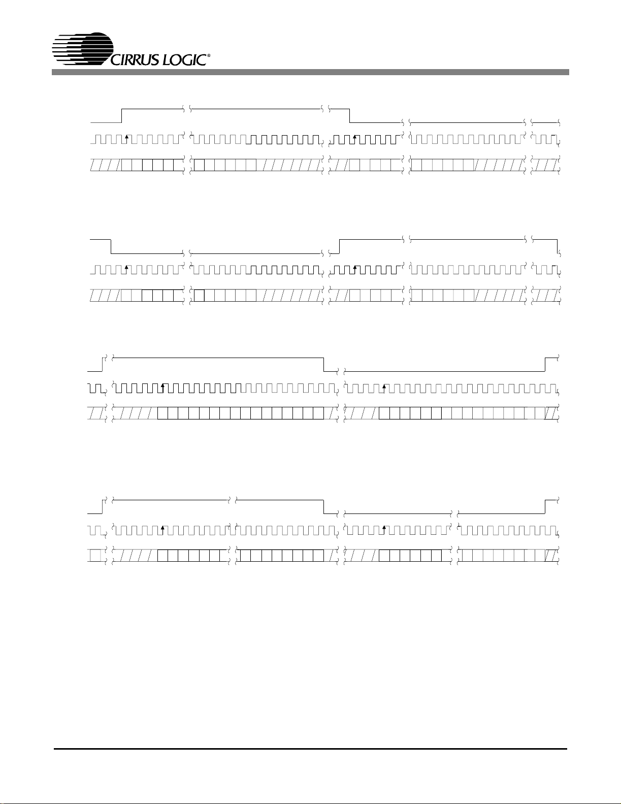
CS4362
LRCK
SCLK
SDINx +3 +2 +1+5 +4-1 -2 -3 -4 -5 +3 +2 +1+5 +4
MSB LSB MSB LSB
Left Channel
-2 -3 -4
-1
Right Channel
Figure 33. Format 0 - L eft Justified up to 24-bit Data
LRCK
SCLK
MSB MSBLSB LSB
SDINx +3 +2 +1+5 +4
-2 -3 -4 -5
-1
Left Channel
-1
-2 -3 -4
Right Channel
Figure 34. Format 1 - I2S up to 24-bit Data
LRCK
SCLK
Left Channel
Right Channel
+3 +2 +1+5 +4
SDINx
LRCK
SCLK
SDINx
15 14 13 12 11 10
32 clocks
6543210987
15 14 13 12 11 10
6543210987
Figure 35. Format 2 - Right Justified 16-bit Data
Left Channel
0
23 22 21 20 19 18
32 clocks
65432107
23 22 21 20 19 18
Right Channel
65432107
Figure 36. Format 3 - Right Justified 24-bit Data
35
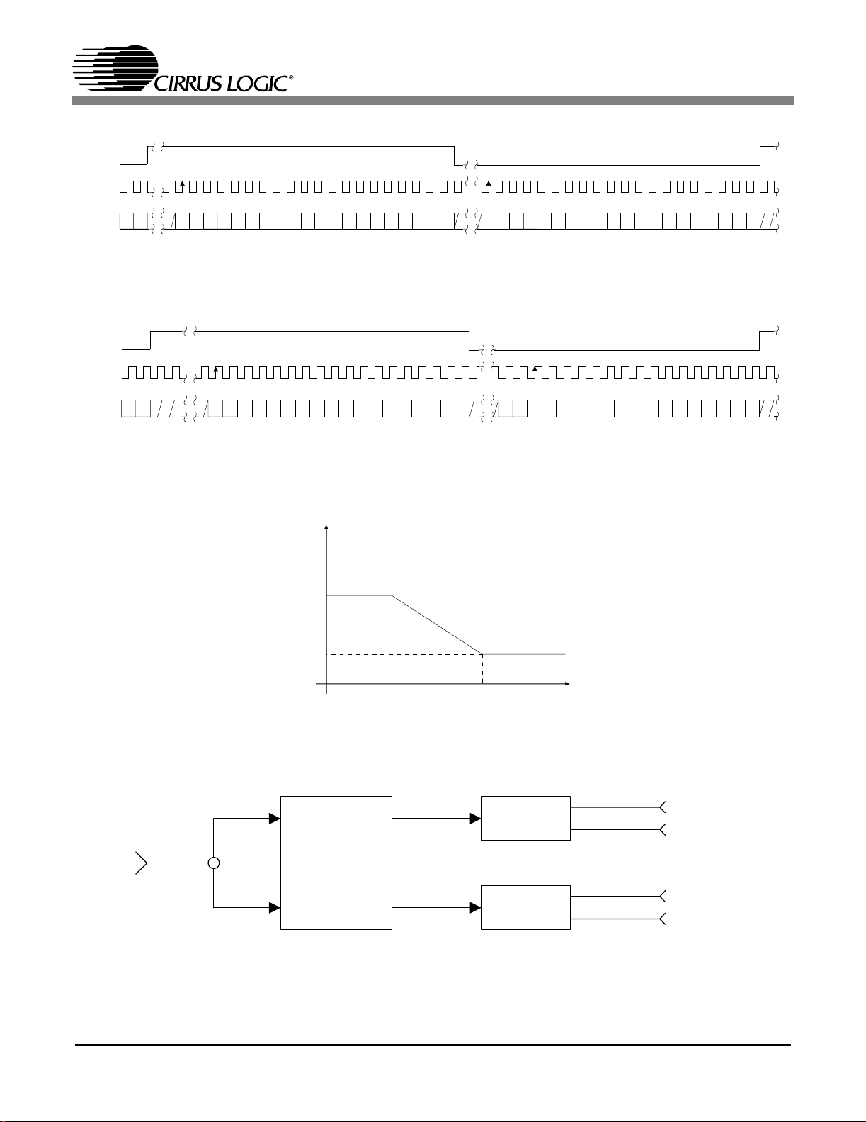
CS4362
LRCK
SCLK
SDINx
10 6543210987
17 16 17 16
19 18 19 18
Left Channel
15 14 13 12 11 10
32 clocks
6543210987
15 14 13 12 11 10
Figure 37. Format 4 - Right Justified 20-bit Data
LRCK
SCLK
SDINx
10
Left Channel
654321098715 14 13 12 11 10
32 clocks
Figure 38. Format 5 - Right Justified 18-bit Data
Gain
dB
Right Channel
Right Channel
654321098715 14 13 12 11 1017 16 17 16
SDINx
T1=50 µs
0dB
T2 = 15 µs
-10dB
F1 F2
3.183 kHz 10.61 kHz
Frequency
Figure 39. De-Emphasis Curve
L
DAC
Channel
Pair x
Control
R
DAC
Figure 40. Cha nnel Pair Routing Diagram (x = Channel Pair 1, 2, or 3)
AOUTAx+
AOUTAx-
AOUTBx+
AOUTBx-
36
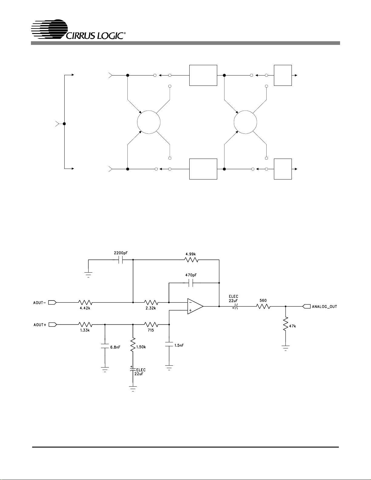
CS4362
SDINx
Left Channel
Audio Data
Right Channel
Audio Data
A Channel
Volume
Control
ΣΣ
B Channel
Volume
Control
Figure 41. ATAPI Block Diagram (x = channel pair 1, 2, or 3)
MUTE
MUTE
AoutAx
AoutBx
Figure 42. Recommended Output Filter
37

7. PARAMETER DEFINITIONS
Total Harmo nic Distortion + Noise (THD+N)
The ratio of the rms value of the signal to the rms sum of all other spectral component s over the specified
bandwidth (typically 10Hz to 20kHz), including distortion components. Expressed in decibels.
Dynamic Range
The ratio of the full scal e rms value of the signal to the rms sum of all other spectral components ov er the
specified bandwidth. Dynamic range is a signal-to-noise measurem ent over the specified bandwi dth
made with a -60 dBFS signal. 60 dB is then added t o the resulting measurement to referthe meas urement
to full scale. This technique ensures that the distortion components are below the noise level and do not
effect the m eas urement. This measurement technique has been accepted by the Audio Engineering Society, AES17-1991, and the Electronic Industries Association of Japan, EIAJ CP-307.
Interchannel Isolation
A measure of crosstalk between the left and right channels. Measured for each channel at the converter's
output with al l zeros to the input under test and a full-scale signal applied to t he ot her cha nnel. Units in
decibels.
Interchannel Gain Mismatch
The gain dif fe re nc e betwee n left and right channels. Units in decibels.
CS4362
Gain Error
The deviation from the nominal full scale analog output for a full scale digital input.
Gain Drift
The change in gain value with temperature. Units in ppm/°C.
8. REFERENCES
1. "How to Achieve Optimum Performance from Delta-Sigma A/D & D/A Converters" by St even Harris.
Paper presented at the 93rd Convention of the Audio Engineering Society, October 1992.
2. CDB4362 E va luation Board Datash eet
3. “Design Notes for a 2-Pole Filter with Differential Input” by Steven Green. Cirrus Logic Application Note
AN48
4. “The I
2
C-Bus Spec ification: Version 2.0” Philips S emiconductors, December 1998.
http://www.semiconductors.philips.com
38

9. PACKAGE DIMENSIONS
48L LQFP PACKAGE DRAWING
D1
D
CS4362
E
E1
1
e
∝
B
A
A1
L
INCHES MILLIMETERS
DIM MIN NOM MAX MIN NOM MAX
A --- 0.055 0.063 --- 1.40 1.60
A1 0.002 0.004 0.006 0.05 0.10 0.15
B 0. 007 0.009 0.011 0.17 0.22 0.27
D 0.343 0.354 0.366 8.70 9.0 BSC 9.30
D1 0.272 0.28 0.280 6.90 7.0 BSC 7.10
E 0. 343 0.354 0.366 8.70 9.0 BSC 9.30
E1 0.272 0.28 0.280 6.90 7.0 BSC 7.10
e* 0.016 0.020 0.024 0.40 0. 50 B SC 0.60
L 0.018 0.24 0. 030 0.45 0.60 0.75
∝
* Nominal pin pitch is 0.50 mm
0.000° 4° 7.000° 0.00° 4° 7.00°
Controlling dimension is mm.
JEDEC Designation: MS022
39

 Loading...