

Page 1
CS4360
24-Bit, 192 kHz 6-channel D/A Converter
Features
24-bit Conversion
102 dB Dynamic Range
-91 dB THD+N
Low Clock Jitter Sensitivity
Digital Volume Control with Soft Ramp
– 119 dB Attenuation
– 1-dB Step Size
– Zero Crossing Click-Free Transitions
ATAPI Mixing
Logic Levels Between 5.0 V and 1.8 V
+3.3 V or +5 V Analog Power Supply
116 mW with 3.3 V Supply
Popguard Technology® for Control of Clicks
and Pops
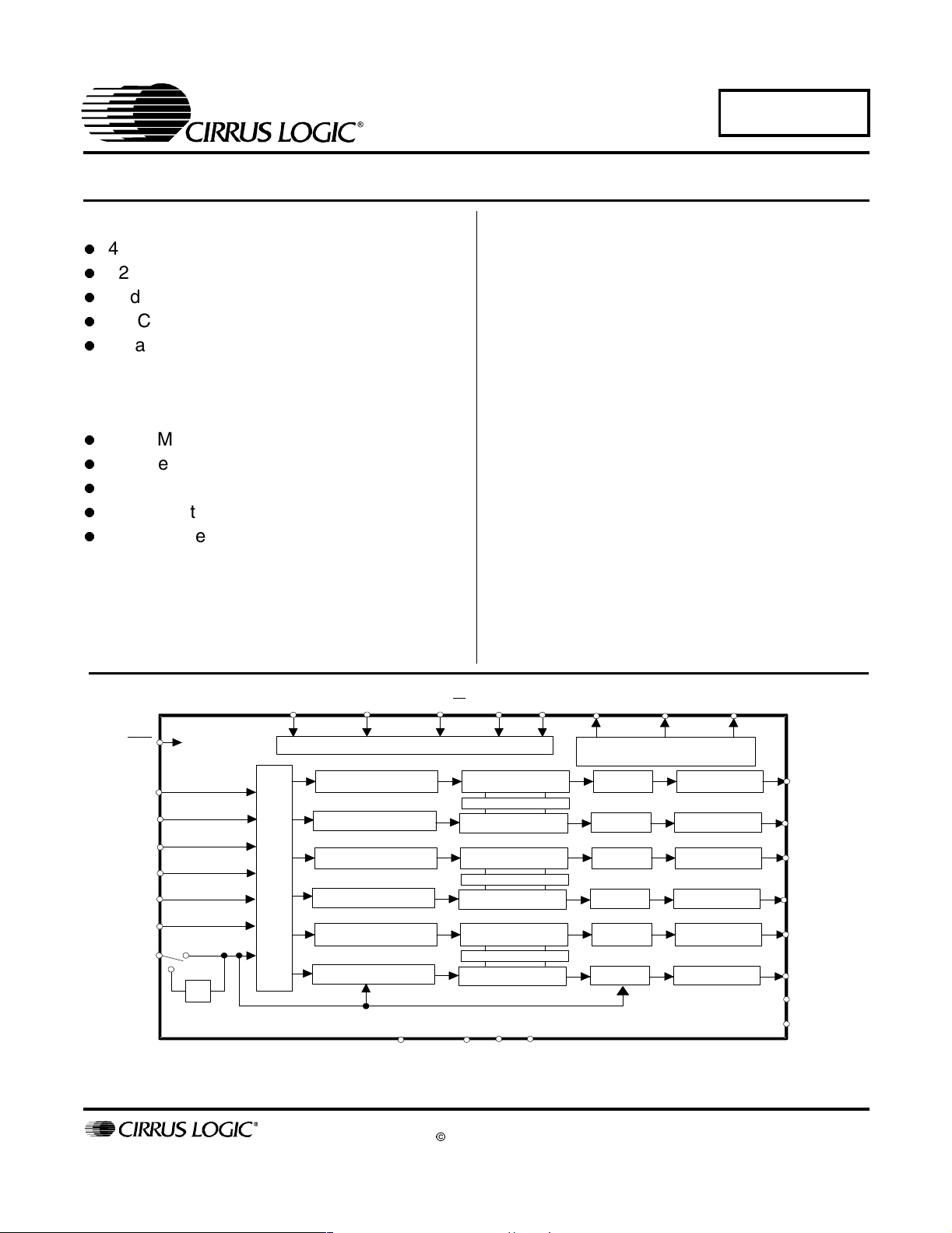
I
Description
The CS4360 is a complete 6-channel digital-to-analog
system including digital interpolation, fourth-order deltasigma digital-to-analog conversion, digital de-emphasis,
volume control, channel mixing and analog filtering. The
advantages of this architecture include: ideal differential
linearity, no distortion mechanisms due to resistor
matching errors, no linearity drift over time and temperature, and a high tolerance to clock jitter.
The CS4360 accepts data at audio sample rates from
4 kHz to 200 kHz, consumes very little power, and operates over a wide power supply range. These features are
ideal for cost-sensitive, multi-channel audio systems including DVD players, A/V receivers, set-top boxes,
digital TVs and VCRs, mini-component systems, and
mixing consoles.
ORDERING INFORMATION
CS4360-KZ -10 to 70 °C 28-pin TSSOP
CS4360-KZZ -10 to 70 °C Lead Free 28-pin TSSOP
CS4360-DZZ -40 to 85 °C Lead Free 28-pin TSSOP
CDB4360 Evaluation Board
RST
VLS
SCLK
LRCK
SD I N1
SD I N2
SD I N3
MCLK
2
÷
http://www.cirrus.com
DIF1/ SCL/CCLK
Serial Port
DIF0/SDA/CDIN M1/AD0/CS
Control Port
Interpolation Filter
Interpolation Filter
Interpolation Filter
VD
Copyright © Cirrus Logic, Inc. 2004
(All Rights Reserved)
VLC
M2
Volume C ontrolInterpolati on Filter Analog Filter AOUT A1
Mixer
Volume Control
Volume C ontrolInterpolation Filter Analog Filter AOUT A2
Mixer
Volume Control
Volume C ontrolInterpolation Filter Analog Filter AOUT A3
Mixer
Volu me Control
VA
GND
GND
MUTEC1 MUTEC2 MUTEC3
External
Mute Control
∆Σ
DAC
∆Σ
DAC
∆Σ
DAC
∆Σ
DAC
∆Σ
DAC
∆Σ
DAC
Analog Filter
Analog Filter
Analog Filter
AO UTB1
AO UTB2
AO UT B3
VQ
FILT+
DS517F2
JUL ‘04
1
Page 2

TABLE OF CONTENTS
1. PIN DESCRIPTION ................................................................................................................... 5
2. TYPICAL CONNECTION DIAGRAM ...................................................................................... 7
3. CHARACTERISTICS AND SPECIFICATIONS ........................................................................ 8
SPECIFIED OPERATING CONDITIONS ................................................................................. 8
ABSOLUTE MAXIMUM RATINGS ........................................................................................... 8
ANALOG CHARACTERISTICS (CS4360-KZ/KZZ) .................................................................. 9
ANALOG CHARACTERISTICS (CS4360-DZZ) ..................................................................... 11
COMBINED INTERPOLATION & ON-CHIP ANALOG FILTER RESPONSE......................... 13
SWITCHING SPECIFICATIONS - SERIAL AUDIO INTERFACE........................................... 16
SWITCHING SPECIFICATIONS - CONTROL PORT INTERFACE ....................................... 17
SWITCHING SPECIFICATIONS - CONTROL PORT INTERFACE ....................................... 18
DC ELECTRICAL CHARACTERISTICS.................................................................................19
DIGITAL INPUT CHARACTERISTICS ...................................................................................19
DIGITAL INTERFACE SPECIFICATIONS..............................................................................20
THERMAL CHARACTERISTICS AND SPECIFICATIONS ....................................................20
4. APPLICATIONS ...................................................................................................................... 21
4.1 Sample Rate Range/Operational Mode Select ................................................................ 21
4.1.1 Stand-alone Mode ............................................................................................... 21
4.1.2 Control Port Mode ............................................................................................... 21
4.2 System Clocking .............................................................................................................. 21
4.3 Digital Interface Format .................................................................................................... 22
4.3.1 Stand-alone Mode ............................................................................................... 22
4.3.2 Control Port Mode ..............................................................................................23
4.4 De-emphasis Control ....................................................................................................... 23
4.4.1 Stand-alone Mode ............................................................................................... 24
4.4.2 Control Port Mode ............................................................................................... 24
4.5 Recommended Power-up Sequence ............................................................................... 24
CS4360
Contacting Cirrus Logic Support
For all product questions and inquiries contact a Cirrus Logic Sales Representative.
To find one nearest you go to http://www.cirrus.com/
IMPORTANT NOTICE
Cirrus Logic, Inc. and its subsidiaries ("Cirrus") believe that the information contained in this document is accurate and reli able. However, the information is subject to change without notice and is provided "AS IS" without warranty of any kind (express or implied). Customers are advi sed to obtain the latest version of
relevant information to verify, before placing orders, that i nformation being relied on is current and complete. All products are sol d subject to the terms and conditions of sale supplied at the time of order acknowledgment, incl uding those pertaini ng to warranty, patent infringement, and l imitation of liability. No responsibility is assumed by Cirrus for the use of this information, includi ng use of this information as the basis for manufacture or sale of any i tems, or for infringement
of patents or other rights of third parties. This document is the property of Cirrus and by furni shing thi s information, Cirrus grants no license, express or implied
under any patents, mask work rights, copyrights, trademarks, trade secrets or other intellectual property rights. Cirrus owns the copyrights associated with the
information contained herein and gives consent for copies to be made of the informati on only for use within your organization with respect to Cirrus integrated
circuits or other products of Cirrus. This consent does not extend to other copying such as copying for general distribution, advertising or promotional purposes,
or for creating any work for resale.
CERTAIN APPLICATIONS USING SEMICONDUCTOR PRODUCTS MAY INVOLVE POTENTIAL RISKS OF DEATH, PERSONAL INJURY, OR SEVERE
PROPERTY OR ENVIRONMENTAL DAMAGE ("CRITICAL APPLICATIONS") . CIRRUS PRODUCTS ARE NOT DESIGNED, AUTHORIZED OR WARRANTED FOR USE I N AIRCRAFT SYSTEMS, MIL ITARY APPLI CATIONS, PRODUCTS SURGICA LLY IMPLANTED I NTO THE BODY, LI FE SUPPORT PRODUCTS
OR OTHER CRITICAL APPLICATIONS (INCLUDING MEDICAL DEVICES, AIRCRAFT SYSTEMS OR COMPONENTS AND PERSONAL OR AUTOMOTIVE
SAFETY OR SECURITY DEVICES). INCLUSION OF CIRRUS PRODUCTS IN SUCH APPLICATIONS IS UNDERSTOOD TO BE FULLY AT THE CUSTOMER'S RISK AND CIRRUS DISCLAIMS AND MAKES NO WARRANTY, EXPRESS, STATUTORY OR IMPLIED, INCLUDING THE IMPLIED WARRANTIES OF
MERCHANTABILITY AND FITNESS FOR PARTI CULAR PURPOSE, WITH REGARD TO ANY CIRRUS PRODUCT THAT IS USED IN SUCH A MANNER. IF
THE CUSTOMER OR CUSTOMER'S CUSTOMER USES OR PERMITS THE USE OF CIRRUS PRODUCTS IN CRITICAL APPLICATIONS, CUSTOMER
AGREES, BY SUCH USE, TO FULLY INDEMNIFY CIRRUS, ITS OFFICERS, DIRECTORS, EMPLOYEES, DISTRIBUTORS AND OTHER AGENTS FROM
ANY AND ALL L IABILITY, INCLUDING ATTORNEYS' FEES AND COSTS, THAT MAY RESULT FROM OR ARISE IN CONNECTI ON WITH THESE USES.
Cirrus Logic, Cirrus, and the Cirrus Logic logo designs are trademarks of Cirrus Logic, Inc. All oth er brand and product names i n this document may be trademarks or servi ce marks of their respective owners.
I²C is a registered trademark of Philips Semiconductor. Purchase of I²C Components of Cirrus Logic, Inc., or one of its sublicensed Associ ated Companies conveys a license under the Philips I²C Patent Rights to use those components in a standard I ²C system.
2 DS517F2
Page 3

CS4360
4.5.1 Stand-alone Mode ............................................................................................... 24
4.5.2 Control Port Mode ............................................................................................... 24
4.6 Popguard
4.6.1 Power-up ............................................................................................................. 24
4.6.2 Power-down ........................................................................................................ 24
4.6.3 Discharge Time ................................................................................................... 25
4.7 Mute Control .................................................................................................................... 25
4.8 Grounding and Power Supply Arrangements .................................................................. 25
4.8.1 Capacitor Placement ........................................................................................... 25
4.8.2 Power Supply Sections ....................................................................................... 25
4.9 Control Port Interface ...................................................................................................... 25
4.9.1 Memory Address Pointer (MAP) ......................................................................... 26
4.9.2 I²C Mode ............................................................................................................. 26
4.9.3 SPI Mode ............................................................................................................ 27
5. REGISTER QUICK REFERENCE ......................................................................................... 29
6. REGISTER DESCRIPTIONS .................................................................................................. 30
6.1 Mode Control 1 (address 01h) ......................................................................................... 30
6.1.1 Auto-mute (AMUTE) Bit 7 ....................................................................................... 30
6.1.2 Digital Interface Format (DIF) Bit 4-6 ...................................................................... 30
6.1.3 De-emphasis Control (DEM) Bit 2-3........................................................................ 31
6.1.4 Functional Mode (FM) Bit 0-1.................................................................................. 31
6.2 Invert Signal (address 02h) ............................................................................................. 31
6.2.1 Invert Signal Polarity (INV_xx) Bit 0-5..................................................................... 31
6.3 Mixing Control Pair 1 (Channels A1 & B1) (address 03h)
Mixing Control Pair 2 (Channels A2 & B2) (address 04h)
Mixing Control Pair 3 (Channels A3 & B3) (address 05h)............................................. 31
6.3.1 ATAPI Channel Mixing and Muting (atapi) Bit 0-3................................................... 32
6.4 Volume Control (addresses 06h - 0Bh) ........................................................................... 33
6.4.1 MUTE (MUTE) Bit 7 ................................................................................................ 33
6.4.2 VOLUME CONTROL (xx_VOL) Bit 0-6................................................................... 33
6.5 Mode Control 2 (address 0Dh) ......................................................................................... 33
6.5.1 Soft Ramp and Zero Cross CONTROL (SZC) Bit 6-7............................................. 33
6.5.2 Control Port Enable (CPEN) Bit 5 ........................................................................... 34
6.5.3 Power Down (PDN) Bit 4......................................................................................... 34
6.5.4 Popguard® Transient Control (POPG) Bit 3 ........................................................... 34
6.5.5 Freeze Controls (FREEZE) Bit 2............................................................................. 35
6.5.6 Master Clock DIVIDE ENABLE (MCLKDIV) Bit 1 ................................................... 35
6.5.7 Single Volume Control (SNGLVOL) Bit 0................................................................ 35
6.6 Revision Register (Read Only) (address 0Dh) ................................................................ 35
6.6.1 Revision Indicator (REV) [Read Only] Bit 0-3 ......................................................... 35
®
Transient Control .......................................................................................... 24
4.9.1a INCR (Auto Map Increment) ................................................................ 26
4.9.1b MAP0-3 (Memory Address Pointer) ..................................................... 26
4.9.2a I²C Write ............................................................................................... 26
4.9.2b I²C Read ............................................................................................... 27
4.9.3a SPI Write .............................................................................................. 28
7. PARAMETER DEFINITIONS .................................................................................................. 36
Total Harmonic Distortion + Noise (THD+N) .......................................................................... 36
Dynamic Range...................................................................................................................... 36
Interchannel Isolation ............................................................................................................. 36
Interchannel Gain Mismatch ................................................................................................... 36
Gain Error............................................................................................................................... 36
Gain Drift ................................................................................................................................ 36
DS517F2 3
Page 4

8. REFERENCES ........................................................................................................................ 36
9. PACKAGE DIMENSIONS ....................................................................................................... 37
LIST OF FIGURES
Figure 1. Typical Connection Diagram .......................................................................................... 7
Figure 2. Output Test Load ......................................................................................................... 10
Figure 3. Maximum Loading ........................................................................................................10
Figure 4. Single-speed Stopband Rejection ................................................................................ 14
Figure 5. Single-speed Transition Band ...................................................................................... 14
Figure 6. Single-speed Transition Band (Detail) ......................................................................... 14
Figure 7. Single-speed Passband Ripple .................................................................................... 14
Figure 8. Double-speed Stopband Rejection .............................................................................. 14
Figure 9. Double-speed Transition Band .....................................................................................14
Figure 10. Double-speed Transition Band (Detail) ........................................................................ 15
Figure 11. Double-speed Passband Ripple ................................................................................... 15
Figure 12. Serial Mode Input Timing .............................................................................................16
Figure 13. Control Port Timing - I²C Mode .................................................................................... 17
Figure 14. Control Port Timing - SPI Mode ...................................................................................18
Figure 15. Left Justified up to 24-Bit Data .....................................................................................23
Figure 16. I
Figure 17. Right Justified Data ...................................................................................................... 23
Figure 18. De-emphasis Curve .....................................................................................................23
Figure 19. I²C Write ....................................................................................................................... 27
Figure 20. I²C Read .......................................................................................................................27
Figure 21. SPI Write ...................................................................................................................... 28
Figure 22. ATAPI Block Diagram ..................................................................................................32
2
S, up to 24-Bit Data ................................................................................................... 23
CS4360
LIST OF TABLES
Table 1. CS4360 Stand-alone Operational Mode............................................................................. 21
Table 2. CS4360 Control Port Operational Mode............................................................................. 21
Table 3. Single-speed Mode Standard Frequencies ........................................................................ 21
Table 4. Double-speed Mode Standard Frequencies ....................................................................... 21
Table 5. Quad-speed Mode Standard Frequencies ......................................................................... 22
Table 6. Digital Interface Format - Stand-alone Mode...................................................................... 22
Table 7. Power Supply Control Sections ..........................................................................................25
Table 8. Digital Interface Formats - Control Port Mode....................................................................30
Table 9. ATAPI Decode.................................................................................................................... 32
Table 10. Example Digital Volume Settings ..................................................................................... 33
4 DS517F2
Page 5
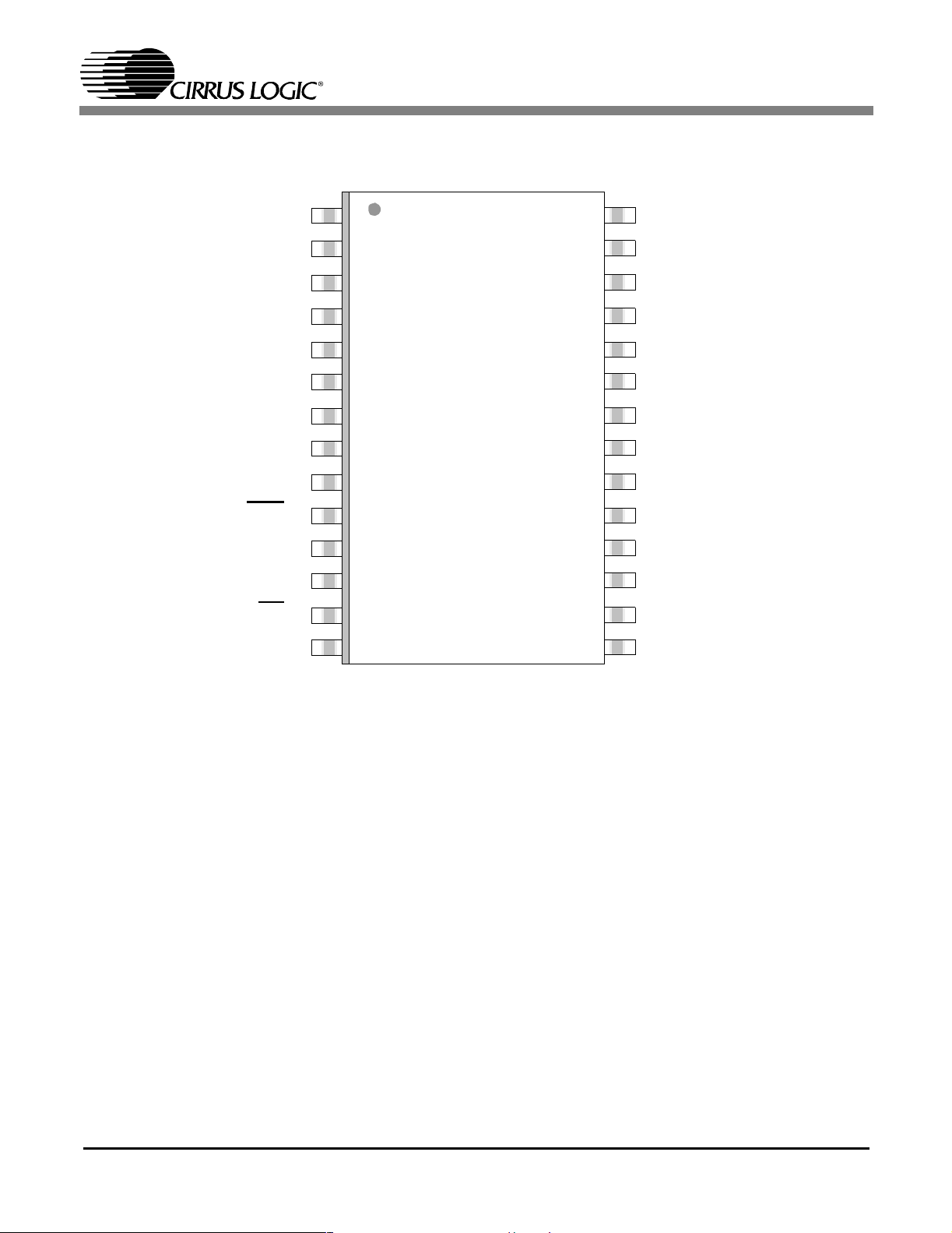
1. PIN DESCRIPTION
CS4360
VLS MUTEC1
SDIN1 AOUTA1
SDIN2 AOUTB1
SDIN3 MUTEC2
SCLK AOUTA2
LRCK AOUTB2
MCLK VA
VD GND
GND AOUTA3
RST
DIF1/SCL/CCLK MUTEC3
DIF0/SDA/CDIN VQ
M1/AD0/CS FILT+
VLC M2
1
2
3
4
5
6
7
821
9
10
11
12 17
13
14 15
CS4360
28
27
26
25
24
23
22
20
19
18
16
AOUTB3
DS517F2 5
Page 6
Pin Name # Pin Description
VLS
SDIN1
SDIN2
SDIN3
SCLK
LRCK
MCLK
VD
GND
Serial Audio Interface Power (Input) - Positive power for the serial audio interface.
1
Serial Audio Data Input (Input) - Input for two’s complement serial audio data.
2
3
4
Serial Clock (Input) - Serial clock for the serial audio interface.
5
Left Right Clock (Input) - Determines which channel, Left or Right, is currently active on the serial audio
6
data line.
Master Clock (Input) - Clock source for the delta-sigma modulator and digital filters.
7
8 Digital Power (Input) - Positive power supply for the digital section.
Ground (Input)
9
21
RST
VLC
FILT+
VQ
VA
AOUTB3
AOUTA3
AOUTB2
AOUTA2
AOUTB1
AOUTA1
MUTEC3
MUTEC2
MUTEC1
Control Port
Definitions
SCL/CCLK
SDA/CDIN
AD0/CS
Stand-Alone
Definitions
DIF1
DIF0
M1
M2
Reset (Input) - Powers down device and resets all internal resisters to their default settings.
10
Control Port Interface Power (Input) - Positive power for the control port interface.
14
Positive Voltage Reference (Output) - Positive reference voltage for the internal sampling circuits.
16
17 Quiescent Voltage (Output) - Filter connection for internal quiescent voltage.
22 Analog Power (Input) - Positive power supply for the analog section.
Analog Outputs (Output) - The full scale analog line output level is specified in the Analog Char acter is-
19
tics and Specifications table.
20
23
24
26
27
Mute Control (Output) - Control signal for optional mute circuit.
18
25
28
Serial Control Port Clock (Input) - Serial clock for the control port interface.
11
12 Serial Control Data I/O (Input/Output) - Input/Output for I²C data. Input for SPI data.
Address Bit / Chip Select (Input) - Chip address bit in I²C Mode. Control signal used to select the chip
13
in SPI mode.
Digital Interface Format (Input) - Defines the required relationship between the Left Right Clock, Serial
11
Clock and Serial Audio Data.
12
13
Mode Selection (Input) - Determines the operational mode of the device.
15
CS4360
6 DS517F2
Page 7
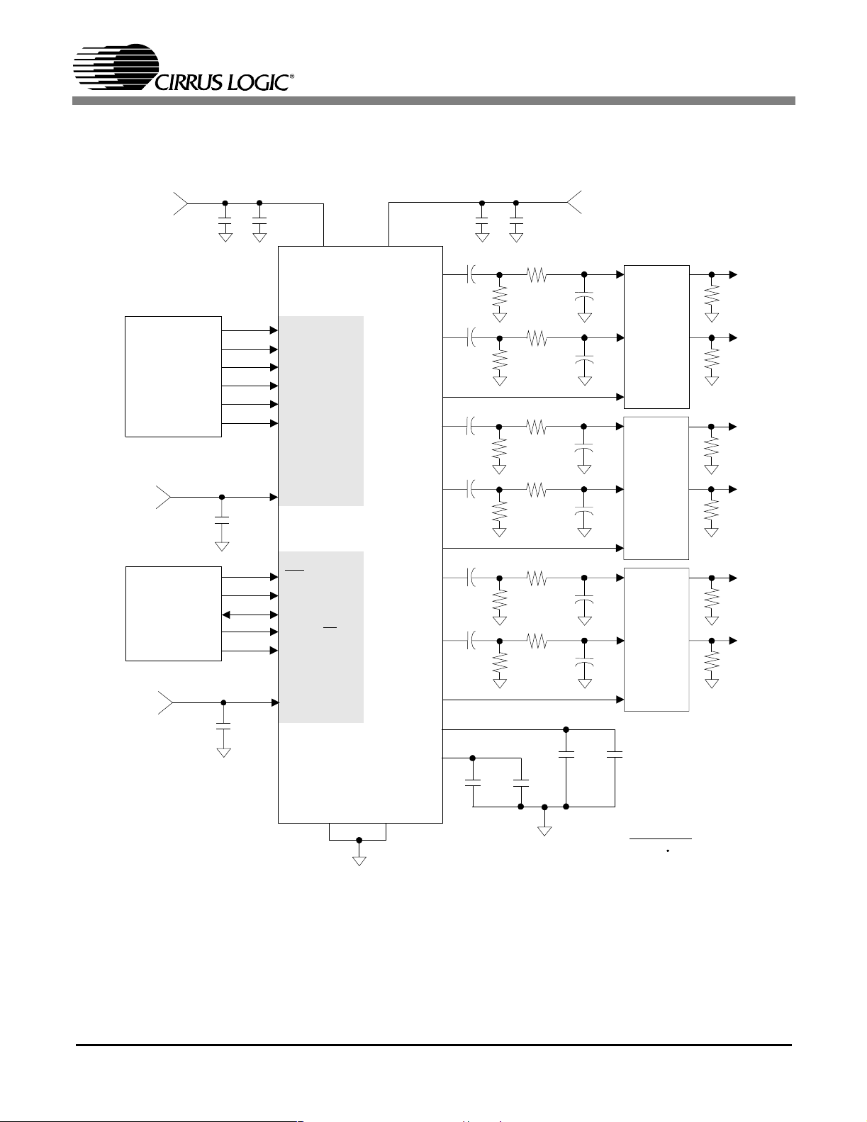
2. TYPICAL CONNECTION DIAGRAM
CS4360
+3.3 V to +5 V *
+1.8 V to +5 V *
Configuration
Digital
Audio
Source
µ C/
Mode
1 µF
0.1 µF
+
0.1 µF
7
MCLK
6
LRCK
5
SCLK
4
SDIN1
3
SDIN2
2
SDIN3
1
VLS
10
RST
11
DIF1/SCL/CCLK
12
DIF0/SDA/CDIN
13
M1/AD0/CS
15
M2
22
VA
CS4360
8
VD
AOUTA1
AOUTB1
MUTEC1
AOUTA2
AOUTB2
MUTEC2
AOUTA3
AOUTB3
0.1 µF
27
+
3.3 µF
26
+
3.3 µF
28
24
+
3.3 µF
23
+
3.3 µF
25
20
+
3.3 µF
19
+
3.3 µF
10 k
10 k
10 k
10 k
10 k
10 k
+
1 µF
560 Ω
Ω
560 Ω
Ω
560 Ω
Ω
560 Ω
Ω
560 Ω
Ω
560 Ω
Ω
+3.3 V to VA *
* All supplies can be tied together
C
OPTIONAL
MUTE
CIRCUIT
C
C
OPTIONAL
MUTE
CIRCUIT
C
C
OPTIONAL
MUTE
CIRCUIT
C
R
L
R
L
R
L
R
L
R
L
R
L
AOUTA1
AOUTB1
AOUTA2
AOUTB2
AOUTA3
AOUTB3
FILT+
VQ
18
16
17
0.1 µ
+
F
C =
3.3 µF
4πFs(R
R
+560
L
560)
L
F
3.3 µF
+
0.1 µ
+1.8 V to +5 V *
0.1 µF
14
VLC
GND
9
MUTEC3
GND
21
Figure 1. Typical Connection Diagram
DS517F2 7
Page 8
CS4360
3. CHARACTERISTICS AND SPECIFICATIONS
Typical performance characteristics are derived from measurements taken at T
characteristics and specifications are guaranteed over the operating temperature and voltages.
SPECIFIED OPERATING CONDITIONS GND = 0 V; all voltages with respect to GND.
Parameters Symbol Min Typ Max Units
DC Power Supply
Analog 3.3 V Nominal
(Note 1) 5.0 V Nominal
Digital 2.5 V Nominal
(Note 1) 3.3 V Nominal
5.0 V Nominal
Serial Audio Interface 1.8 V Nominal
2.5 V Nominal
3.3 V Nominal
5.0 V Nominal
Control Port Interface 1.8 V Nominal
2.5 V Nominal
3.3 V Nominal
5.0 V Nominal
VA 3.0
VD 2.25
VLS 1.7
VLC 1.7
= 25°C. Min/Max performance
A
4.5
3.0
4.5
2.25
3.0
4.5
2.25
3.0
4.5
3.3
5
2.5
3.3
5
1.8
2.5
3.3
5
1.8
2.5
3.3
5
3.6
5.5
2.75
3.6
5.5
1.9
2.75
3.6
5.5
1.9
2.75
3.6
5.5
V
V
V
V
V
V
V
V
V
V
V
V
V
ABSOLUTE MAXIMUM RATINGS
GND = 0 V; all voltages with respect to GND. Operation beyond these limits may result in permanent damage to
the device. Normal operation is not guaranteed at these extremes.
Parameters Symbol Min Max Units
DC Power Supply Analog
Digital
Serial Audio Interface
Control Port Interface
Input Current
(Note 2) I
Digital Input Voltage Serial Audio Interface
Control Port Interface
Ambient Operating Temperature (power applied) T
Storage Temperature T
Notes: 1. Nominal VD supply must be less than or equal to the nominal VA supply.
2. Any pin except supplies.
VA
VD
VLS
VLC
V
IND_S
V
IND_C
in
stg
-0.3
-0.3
-0.3
-0.3
6.0
6.0
6.0
6.0
V
V
V
V
-±10mA
-0.3
-0.3
A
-55 125 °C
VLS+0.4
VLC+0.4
V
V
-65 150 °C
8 DS517F2
Page 9

CS4360
ANALOG CHARACTERISTICS (CS4360-KZ/KZZ)
Test conditions (unless otherwise specified): Input test signal is a 997 Hz sine wave at 0 dBFS; measurement
bandwidth is 10 Hz to 20 kHz; test load R
Parameter
Single-Speed Mode Fs = 48 kHz
Dynamic Range
Total Harmonic Distortion + Noise
Double-Speed Mode Fs = 96 kHz
Dynamic Range
40 kHz Bandwidth A-Weighted
Total Harmonic Distortion + Noise
Quad-Speed Mode Fs = 192 kHz
Dynamic Range
40 kHz Bandwidth A-Weighted
Total Harmonic Distortion + Noise
=10kΩ, CL = 10 pF (see Figure 2). All supplies = VA = 5.0 V or 3.3 V.
L
5.0 V 3.3 V
Min Typ Max Min Typ Max Unit
(Note 3)
unweighted
A-Weighted
A-Weighted
(Note 3)
0 dB
-20 dB
-60 dB
(Note 3)
unweighted
A-Weighted
(Note 3)
0 dB
-20 dB
-60 dB
(Note 3)
unweighted
A-Weighted
(Note 3)
0 dB
-20 dB
-60 dB
94
97
94
97
94
97
99
102
-
100
-
-91
-
-79
-
-39
99
102
-
100
-
-91
-
-79
-
-39
99
102
-
100
-
-91
-
-79
-
-39
-
-
-
-86
-
-
-
-
-
-86
-
-
-
-
-
-86
-
-
89
92
89
92
89
92
94
97
-
-
-
-
97
-91
-74
-34
94
97
-
-
-
-
97
-91
-74
-34
94
97
-
-
-
-
97
-91
-74
-34
-
-
-
-86
-
-
-
-
-
-86
-
-
-
-
-
-86
-
-
dB
dB
dB
dB
dB
dB
dB
dB
dB
dB
dB
dB
dB
dB
dB
dB
dB
dB
Notes: 3. One-half LSB of triangular PDF dither is added to data.
DS517F2 9
Page 10
CS4360
ANALOG CHARACTERISTICS (CS4360-KZ/KZZ) (Continued)
Parameters Symbol Min Typ Max Units
Dynamic Performance for All Modes
Interchannel Isolation (1 kHz) - 102 - dB
DC Accuracy
Interchannel Gain Mismatch ICGM - 0.1 - dB
Gain Drift - ±100 - ppm/°C
Analog Output Characteristics and Specifications
Full Scale Output Voltage 0.60•VA 0.66•VA 0.72•VA Vpp
Output Impedance Z
Minimum AC-Load Resistance
Maximum Load Capacitance
(Note 4) R
(Note 4) C
4. Refer to Figure 3.
.
out
L
L
125
- 100 - Ω
-3-kΩ
- 100 - pF
AGND
3.3 µF
AOUTx
+
Figure 2. Output Test Load
100
L
V
out
R
L
C
L
75
50
25
Capacitive Load -- C (pF)
2.5
51015
3
Safe Operating
Region
Resistive Load -- R (kΩ)
L
20
Figure 3. Maximum Loading
10 DS517F2
Page 11
CS4360
ANALOG CHARACTERISTICS (CS4360-DZZ)
Test conditions (unless otherwise specified): Input test signal is a 997 Hz sine wave at 0 dBFS; measurement
bandwidth is 10 Hz to 20 kHz; test load R
Parameter
Single-speed Mode Fs = 48 kHz
Dynamic Range
Total Harmonic Distortion + Noise
Double-speed Mode Fs = 96 kHz
Dynamic Range
40 kHz Bandwidth A-Weighted
Total Harmonic Distortion + Noise
Quad-speed Mode Fs = 192 kHz
Dynamic Range
40 kHz Bandwidth A-Weighted
Total Harmonic Distortion + Noise
= 10 kΩ, CL = 10 pF (see Figure 2). All supplies = VA = 5.0 V and 3.3 V.
L
VA = 5.0 V VA = 3.3 V
Min Typ Max Min Typ Max Unit
(Note 3)
unweighted
A-Weighted
A-Weighted
(Note 3)
0 dB
-20 dB
-60 dB
(Note 3)
unweighted
A-Weighted
(Note 3)
0 dB
-20 dB
-60 dB
(Note 3)
unweighted
A-Weighted
(Note 3)
0 dB
-20 dB
-60 dB
89
92
89
92
89
92
99
102
-
100
-
-91
-
-79
-
-39
99
102
-
100
-
-91
-
-79
-
-39
99
102
-
100
-
-91
-
-79
-
-39
-
-
-
-84
-
-
-
-
-
-84
-
-
-
-
-
-84
-
-
89
92
89
92
89
92
94
97
-
-
-
-
97
-91
-74
-34
94
97
-
-
-
-
97
-91
-74
-34
94
97
-
-
-
-
97
-91
-74
-34
-
-
-
-84
-
-
-
-
-
-84
-
-
-
-
-
-84
-
-
dB
dB
dB
dB
dB
dB
dB
dB
dB
dB
dB
dB
dB
dB
dB
dB
dB
dB
DS517F2 11
Page 12

CS4360
ANALOG CHARACTERISTICS (CS4360-DZZ) (Continued)
Parameters Symbol Min Typ Max Units
Dynamic Performance for All Modes
Interchannel Isolation (1 kHz) - 102 - dB
DC Accuracy
Interchannel Gain Mismatch ICGM - 0.1 - dB
Gain Drift - ±100 - ppm/°C
Analog Output Characteristics and Specifications
Full Scale Output Voltage 0.60•VA 0.66•VA 0.72•VA Vpp
Output Impedance Z
AC-load Resistance
Load Capacitance
(Note 4) R
(Note 4) C
out
L
L
- 100 - Ω
3--kΩ
--100pF
12 DS517F2
Page 13

CS4360
COMBINED INTERPOLATION & ON-CHIP ANALOG FILTER RESPONSE
The filter characteristics and the X-axis of the response plots have been normalized to the sample rate (Fs) and can
be referenced to the desired sample rate by multiplying the given characteristic by Fs.
Parameter Min Typ Max Unit
Single-Speed Mode (4 kHz to 50 kHz sample rates)
Passband
to -0.05 dB corner
to -3 dB corner
Frequency Response 10 Hz to 20 kHz -0.02 - +0.035 dB
StopBand 0.5465 - - Fs
StopBand Attenuation
Group Delay - 9/Fs - s
De-emphasis Error (Relative to 1 kHz)
Control Port Mode Fs = 32 kHz
Fs = 44.1 kHz
(Note 5) 50 - - dB
(Note 6)
Fs = 48 kHz
0
0
-
-
-
-
-
-
-
-
0.4535
0.4998
+0.2/-0.1
+0.05/-0.14
+0/-0.22
Fs
Fs
dB
dB
dB
Stand-alone Mode Fs = 32 kHz
Fs = 44.1 kHz
Fs = 48 kHz
Double-Speed Mode (50 kHz to 100 kHz sample rates)
Passband
to -0.1 dB corner
to -3 dB corner
Frequency Response 10 Hz to 20 kHz -0.1 - 0 dB
StopBand 0.577 - - Fs
StopBand Attenuation
Group Delay - 4/Fs - s
Quad-Speed Mode - (100 kHz to 200 kHz sample rates)
Passband
to -3 dB corner
Frequency Response 10 Hz to 20 kHz -0.7 - 0 dB
Group Delay - 1.5/Fs - s
Notes: 5. For Single-speed Mode, the measurement bandwidth is 0.5465 Fs to 3 Fs.
For Double-speed Mode, the measurement bandwidth is 0.577 Fs to 1.4 Fs.
6. De-emphasis is only available in Single-speed Mode.
(Note 5) 55 - - dB
-
-
-
0
0
0 - 0.25 Fs
-
-
-
-
-
+1.5/-0
+0.05/-0.14
+0.2/-0.4
0.4621
0.4982
dB
dB
dB
Fs
Fs
DS517F2 13
Page 14

CS4360
Figure 4. Single-speed Stopband Rejection Figure 5. Single-speed Transition Band
Figure 6. Single-speed Transition Band (Detail) Figure 7. Single-speed Passband Ripple
Figure 8. Double-speed Stopband Rejection Figure 9. Double-speed Transition Band
14 DS517F2
Page 15

CS4360
Figure 10. Double-speed Transition Band (Detail) Figure 11. Double-speed Passband Ripple
DS517F2 15
Page 16

CS4360
SWITCHING SPECIFICATIONS - SERIAL AUDIO INTERFACE
Inputs: Logic 0 = GND, Logic 1 = VLS.
Parameters Symbol Min Max Units
MCLK Frequency 1.024 51.2 MHz
MCLK Duty Cycle 40 60 %
Input Sample Rate Single-speed Mode
Double-speed Mode
Quad-speed Mode
F
s
F
s
F
s
4
50
100
LRCK Duty Cycle 45 55 %
SCLK Pulse Width Low t
SCLK Pulse Width High t
SCLK Frequency Single-speed Mode
Double-speed Mode
Quad-speed Mode (MCLKDIV = 0)
Quad-speed Mode (MCLKDIV = 1)
SCLK rising to LRCK edge delay t
SCLK rising to LRCK edge setup time t
SDINx valid to SCLK rising setup time t
SCLK rising to SDINx hold time t
sclkl
sclkh
slrd
slrs
sdlrs
sdh
20 - ns
20 - ns
-
-
-
-
20 - ns
20 - ns
20 - ns
20 - ns
50
100
200
128xFs
64xFs
MCLK
------------ ----2
MCLK
------------ ----4
kHz
kHz
kHz
Hz
Hz
Hz
Hz
LRCK
SCLK
SDINx
t
t
slrd
t
sdlrs
Figure 12. Serial Mode Input Timing
slrs
t
sclkl
t
sdh
t
sclkh
16 DS517F2
Page 17

SWITCHING SPECIFICATIONS - CONTROL PORT INTERFACE
2
s
-
-- -
1
s
-
--
6
s
-
--
Inputs: Logic 0 = GND, Logic 1 = VLC
Parameter Symbol Min Max Unit
I²C Mode
SCL Clock Frequency f
RST
Rising Edge to Start
Bus Free Time Between Transmissions t
Start Condition Hold Time (prior to first clock pulse) t
Clock Low time t
Clock High Time t
Setup Time for Repeated Start Condition t
SDA Hold Time from SCL Falling
(Note 7) t
SDA Setup time to SCL Rising t
Rise Time of SCL and SDA t
Fall Time SCL and SDA t
Setup Time for Stop Condition t
Acknowledge Delay from SCL Falling
(Note 8) t
scl
t
irs
buf
hdst
low
high
sust
hdd
sud
, t
rc
, t
fc
susp
ack
rc
fc
- 100 kHz
500 - ns
4.7 - µs
4.0 - µs
4.7 - µs
4.0 - µs
4.7 - µs
0-µs
250 - ns
-1µs
- 300 ns
4.7 - µs
- (Note 9) ns
CS4360
Notes: 7. Data must be held for sufficient time to bridge the transition time, t
8. The acknowledge delay is based on MCLK and can limit the maximum transaction speed.
9. for Single-Speed Mode, for Double-Speed Mode, for Quad-Speed Mode.
5
----------------56 F
×
5
-----------------28 F
×
RST
t
SDA
SCL
irs
Stop Sta rt
t
buf
t
t
hdst
low
t
high
t
hdd
t
sud
t
ack
Figure 13. Control Port Timing - I²C Mode
Re peated
, of SCL.
fc
--------------4F
Start
t
sust
5
×
t
t
hdst
Stop
rd
t
rc
t
fd
t
fc
t
susp
DS517F2 17
Page 18

CS4360
SWITCHING SPECIFICATIONS - CONTROL PORT INTERFACE (Continued)
Parameter Symbol Min Max Unit
SPI Mode
CCLK Clock Frequency f
RST
Rising Edge to CS Falling
CCLK Edge to CS
CS
High Time Between Transmissions
CS
Falling to CCLK Edge
Falling (Note 10)
CCLK Low Time t
CCLK High Time t
CDIN to CCLK Rising Setup Time t
CCLK Rising to DATA Hold Time
Rise Time of CCLK and CDIN
Fall Time of CCLK and CDIN
(Note 11) t
(Note 12) t
(Note 12) t
sclk
t
srs
t
spi
t
csh
t
css
scl
sch
dsu
dh
r2
f2
-6MHz
500 - ns
500 - ns
1.0 - µs
20 - ns
1
------------ ----MCLK
1
------------ ----MCLK
-ns
-ns
40 - ns
15 - ns
- 100 ns
- 100 ns
Notes: 10. t
11. Data must be held for sufficient time to bridge the transition time of CCLK.
12. For f
only needed before first falling edge of CS after RST rising edge. t
spi
< 1 MHz.
sclk
RST
CS
CCLK
CDIN
t
srs
t
t
css
spi
t
r2
Figure 14. Control Port Timing - SPI Mode
t
scl
t
f2
t
dsu
t
sch
t
dh
= 0 at all other times.
spi
t
csh
18 DS517F2
Page 19

CS4360
DC ELECTRICAL CHARACTERISTICS GND = 0 V; all voltages with respect to GND.
Parameters Symbol Min Typ Max Units
Normal Operation
Power Supply Current VA = 5.0 V
(Note 13)
VD = 5.0 V
I
A
I
D
-
-
22
25
-
-
mA
mA
VA = 3.3 V
VD = 3.3 V
VLS = 5.0 V
VLC = 5.0 V
VLS = 3.3 V
VLC = 3.3 V
(Note 14)
Power Dissipation All Supplies = 5.0 V
All Supplies = 3.3 V
Power-d ow n Mo de
(Note 15)
Power Supply Current All Supplies = 5.0 V
All Supplies = 3.3 V
Power Dissipation All Supplies = 5.0 V
All Supplies = 3.3 V
I
A
I
D
I
LS
I
LC
I
LS
I
LC
-
-
-
-
-
-
-
-
-
-
-
-
21
14
6
2
2
1
235
116
16
12
80
40
-
-
-
-
-
-
265
128
-
-
-
-
mA
mA
µA
µA
µA
µA
mW
mW
µA
µA
µW
µW
All Modes of Operation
Power Supply Rejection Ratio
V
Nominal Voltage
Q
(Note 16) 1 kHz
Output Impedance
Maximum allowable DC current source/sink
Filt+ Nominal Voltage
Output Impedance
Maximum allowable DC current source/sink
60 Hz
PSRR -
60
-
-
-
-
-
-
-
40
0.5•VA
250
0.01
VA
250
0.01
-
-
-
-
-
-
-
-
dB
dB
V
kΩ
mA
V
kΩ
mA
MUTEC Low-level Output Voltage - 0 - V
MUTEC High-level Output Voltage - VA - V
Maximum MUTEC Drive Current - 3 - mA
Notes: 13. Normal operation is defined as RST
= HI with a 997 Hz, 0 dBFS input sampled at the highest Fs for each
speed mode, and open outputs, unless otherwise specified.
14. I
15. Power Down Mode is defined as RST
measured with no external loading on pin 12 (SDA).
LC
= LO with all clocks and data lines held static.
16. Valid with the recommended capacitor values on FILT+ and VQ as shown in Figure 1. Increasing the
capacitance will also increase the PSRR.
DIGITAL INPUT CHARACTERISTICS GND = 0 V; all voltages with respect to GND.
Parameters Symbol Min Typ Max Units
Input Leakage Current I
in
Input Capacitance - 8 - pF
DS517F2 19
--±10µA
Page 20

CS4360
DIGITAL INTERFACE SPECIFICATIONS GND = 0 V; all voltages with respect to GND.
Parameters Symbol Min Max Units
1.8 V Logic
High-level Input Voltage Serial Audio
Control Port
Low-level Input Voltage Serial Audio
Control Port
2.5 V Logic
High-level Input Voltage Serial Audio
Control Port
Low-level Input Voltage Serial Audio
Control Port
3.3 V Logic
High-level Input Voltage Serial Audio
Control Port
Low-level Input Voltage Serial Audio
Control Port
5.0 V Logic
High-level Input Voltage Serial Audio
Control Port
Low-level Input Voltage Serial Audio
Control Port
V
IH
V
IH
V
IL
V
IL
V
IH
V
IH
V
IL
V
IL
V
IH
V
IH
V
IL
V
IL
V
IH
V
IH
V
IL
V
IL
80%
80%
-
70%
70%
-
70%
70%
-
70%
70%
-
-
-
13%
13%
-
-
13%
13%
-
-
13%
13%
-
-
13%
13%
VLS
VLC
VLS
VLC
VLS
VLC
VLS
VLC
VLS
VLC
VLS
VLC
VLS
VLC
VLS
VLC
THERMAL CHARACTERISTICS AND SPECIFICATIONS
Parameters Symbol Min Typ Max Units
Package Thermal Resistance TSSOP (-KZ/KZZ & -DZZ) θ
Ambient Operating Temperature (Power Applied) -KZ/KZZ
-DZZ
JA
T
A
-40-°C/Watt
-10
-40
-
+70
-
+85
°C
°C
20 DS517F2
Page 21

CS4360
4. APPLICATIONS
4.1 Sample Rate Range/Operational Mode Select
4.1.1 Stand-Alone Mode
The device operates in one of four operational modes determined by the Mode pins in Stand-alone mode.
Sample rates outside the specified range for each mode are not supported.
M2 M1 Input Sample Rate (FS)MODE
0 0 4 kHz - 50 kHz Single-Speed (without De-emphasis)
0 1 32 kHz - 48 kHz Single-Speed (with De-emphasis)
1 0 50 kHz - 100 kHz Double-Speed
1 1 100 kHz - 200 kHz Quad-Speed
Table 1. CS4360 Stand-Alone Operational Mode
4.1.2 Control Port Mode
The device operates in one of three operational modes determined by the FM bits (see section 6.1.4) in
Control Port mode. Sample rates outside the specified range for each mode are not supported.
FM1 FM0 Input Sample Rate (FS)MODE
0 0 4 kHz - 50 kHz Single-speed
0 1 50 kHz - 100 kHz Double-speed
1 0 100 kHz - 200 kHz Quad-speed
1 1 Reserved Reserved
Table 2. CS4360 Control Port Operational Mode
4.2 System Clocking
The device requires external generation of the master (MCLK), left/right (LRCK) and serial (SCLK) clocks.
The LRCK, defined also as the input sample rate (Fs), must be synchronously derived from the MCLK
according to specified ratios. The specified ratios of MCLK to LRCK, along with several standard audio
sample rates and the required MCLK frequency, are illustrated in Tables 3-5.
Sample Rate
(kHz)
32 8.1920 12.2880 16.3840 24.5760 32.7680
44.1 11.2896 16.9344 22.5792 33.8688 45.1584
48 12.2880 18.4320 24.5760 36.8640 49.1520
256x 384x 512x 768x 1024x*
Table 3. Single-speed Mode Standard Frequencies
MCLK (MHz)
Sample Rate
(kHz)
64 8.1920 12.2880 16.3840 24.5760 32.7680
88.2 11.2896 16.9344 22.5792 33.8688 45.1584
96 12.2880 18.4320 24.5760 36.8640 49.1520
128x 192x 256x 384x 512x*
Table 4. Double-speed Mode Standard Frequencies
MCLK (MHz)
DS517F2 21
Page 22

CS4360
Sample Rate
(kHz)
176.4 11.2896 16.9344 22.5792 33.8688 45.1584
192 12.2880 18.4320 24.5760 36.8640 49.1520
64x 96x 128x 192x 256x*
Table 5. Quad-speed Mode Standard Frequencies
MCLK (MHz)
*Requires MCLKDIV bit = 1 in the Mode Control 2 register (address 0Ch)
4.3 Digital Interface Format
The device will accept audio samples in 1 of 4 digital interface formats in Stand-alone mode, as illustrated
in Table 6, and 1 of 6 formats in Control Port mode, as illustrated in Table 8.
4.3.1 Stand-Alone Mode
The desired format is selected via the DIF1 and DIF0 pins. For an illustration of the required relationship
between the LRCK, SCLK and SDIN, see Figures 15-17.
DIF1 DIF0 DESCRIPTION FORMAT FIGURE
00
01
10
11
Left Justified, up to 24-bit Data
I2S, up to 24-bit Data
Right Justified, 16-bit Data
Right Justified, 24-bit Data
Table 6. Digital Interface Format - Stand-alone Mode
016
115
217
317
22 DS517F2
Page 23

CS4360
4.3.2 Control Port Mode
The desired format is selected via the DIF2, DIF1 and DIF0 bits in the Mode Control 2 register (see section
6.1.2). For an illustration of the required relationship between LRCK, SCLK and SDIN, see Figures 15-17.
LRCK
SCLK
SDIN +3 +2 +1+5 +4
MSB
-1 -2 -3 -4 -5
Left Channel
LRCK
SCLK
SDIN +3 +2 +1+5 +4
MSB
-1 -2 -3 -4 -5
LRCK
SCLK
Left Channel
Left Channel
LSB
MSB
-1 -2 -3 -4
Figure 15. Left Justified up to 24-Bit Data
LSB LSB
MSB
-1 -2 -3 -4
Figure 16. I2S, up to 24-Bit Data
Right Channel
+3 +2 +1+5 +4
Right Channel
+3 +2 +1+5 +4
Right Channel
LSB
SDIN
MSB LSB
+6 +5 +4 +3 +2 +1+7-1 -2 -3 -4 -5LSB
MSB LSB
+6 +5 +4 +3 +2 +1+7-1 -2 -3 -4 -5
Figure 17. Right Justified Data
4.4 De-Emphasis Control
The device includes on-chip digital de-emphasis. Figure 18 shows the de-emphasis curve for Fs equal to
44.1 kHz. The frequency response of the de-emphasis curve will scale proportionally with changes in
sample rate, Fs.
Gain
dB
T1=50 µs
0dB
T2 = 15 µs
-10dB
F1 F2
3.183 kHz 10.61 kHz
Figure 18. De-emphasis Curve
Notes: De-emphasis is only available in Single-speed Mode.
Frequency
DS517F2 23
Page 24

CS4360
4.4.1 Stand-Alone Mode
The operational mode pins, M2 and M1, selects the 44.1 kHz de-emphasis filter. Please see section 4.1
for the desired de-emphasis control.
4.4.2 Control Port Mode
The Mode Control bits selects either the 32, 44.1, or 48 kHz de-emphasis filter. Please see section 6.1.3
for the desired de-emphasis control.
4.5 Recommended Power-up Sequence
4.5.1 Stand-Alone Mode
1) Hold RST low until the power supply and configuration pins are stable, and the master and left/right
clocks are locked to the appropriate frequencies, as discussed in section 4.2. In this state, the control
port is reset to its default settings and VQ will remain low.
2) Bring RST
alone power-up sequence after approximately 512 LRCK cycles in Single-Speed Mode (1024 LRCK
cycles in Double-Speed Mode, and 2048 LRCK cycles in Quad-Speed Mode).
high. The device will remain in a low power state with VQ low and will initiate the Stand-
4.5.2 Control Port Mode
1) Hold RST low until the power supply is stable, and the master and left/right clocks are locked to the
appropriate frequencies, as discussed in section 4.2. In this state, the control port is reset to its default
settings and VQ will remain low.
2) Bring RST
3) Load the desired register settings while keeping the PDN bit set to 1.
4) Set the PDN bit to 0. This will initiate the power-up sequence, which lasts approximately 50 µS when
the POPG bit is set to 0. If the POPG bit is set to 1, see Section 4.6 for a complete description of power-up timing.
high. The device will remain in a low power state with VQ low.
4.6 Popguard® Transient Control
The CS4360 uses a novel technique to minimize the effects of output transients during power-up and power-down. This technology, when used with external DC-blocking capacitors in series with the audio outputs, minimizes the audio transients commonly produced by single-ended single-supply converters. It is
activated inside the DAC when the RST
control, aside from choosing the appropriate DC-blocking capacitors.
pin or PDN bit is enabled/disabled and requires no other external
4.6.1 Power-up
When the device is initially powered-up, the audio outputs, AOUTAx and AOUTBx, are clamped to GND.
Following a delay of approximately 1000 LRCK cycles, each output begins to ramp toward the quiescent
voltage. Approximately 10,000 LRCK cycles later, the outputs reach VQ and audio output begins. This
gradual voltage ramping allows time for the external DC-blocking capacitors to charge to the quiescent
voltage, minimizing the power-up transient.
4.6.2 Power-down
To prevent transients at power-down, the device must first enter its power-down state. When this occurs,
audio output ceases and the internal output buffers are disconnected from AOUTAx and AOUTBx. In their
place, a soft-start current sink is substituted which allows the DC-blocking capacitors to slowly discharge.
Once this charge is dissipated, the power to the device may be turned off and the system is ready for the
next power-on.
24 DS517F2
Page 25

CS4360
4.6.3 Discharge Time
To prevent an audio transient at the next power-on, the DC-blocking capacitors must fully discharge before turning on the power or exiting the power-down state. If full discharge does not occur, a transient will
occur when the audio outputs are initially clamped to GND. The time that the device must remain in the
power-down state is related to the value of the DC-blocking capacitance and the output load. For example,
with a 3.3 µF capacitor, the minimum power-down time will be approximately 0.4 seconds.
4.7 Mute Control
The Mute Control pins go high during power-up initialization, reset, muting (see section 6.1.1 and 6.4.1),
or if the MCLK to LRCK ratio is incorrect. These pins are intended to be used as control for external mute
circuits to prevent the clicks and pops that can occur in any single-ended single supply system.
Use of the Mute Control function is not mandatory but recommended for designs requiring the absolute
minimum in extraneous clicks and pops. Also, use of the Mute Control function can enable the system
designer to achieve idle channel noise/signal-to-noise ratios which are only limited by the external mute
circuit. Please see the CDB4360 data sheet for a suggested mute circuit.
4.8 Grounding and Power Supply Arrangements
As with any high-resolution converter, the CS4360 requires careful attention to power supply and grounding arrangements if its potential performance is to be realized. Figure 1 shows the recommended power
arrangements, with VA, VD, VLS and VLC connected to clean supplies. If the ground planes are split between digital ground and analog ground, the GND pins of the CS4360 should be connected to the analog
ground plane.
All signals, especially clocks, should be kept away from the FILT+ and VQ pins in order to avoid unwanted
coupling into the modulators. The CDB4360 evaluation board demonstrates the optimum layout and power supply arrangements.
4.8.1 Capacitor Placement
Decoupling capacitors should be placed as close to the DAC as possible, with the low-value ceramic capacitor being the closest. To further minimize impedance, these capacitors should be located on the same
layer as the DAC. If desired, all supply pins may be connected to the same supply, but a decoupling capacitor should still be placed on each supply pin and referenced to analog ground.
4.8.2 Power Supply Sections
Each power supply pin provides power to specific sections of the CS4360. The logic voltage level for each
section must adhere to the corresponding power supply voltage setting. For example: If VLC = 1.8 V; VLS
= 3.3 V; VD = VA = 5 V; then the logic level for all mode configuration inputs must equal 1.8 V.
Pin #s Description Power Supply Reference
2, 3, 4, 5, 6, 7
10, 11, 12, 13, 15
Serial Audio Interface Inputs
Mode Configuration Inputs
Table 7. Power Supply Control Sections
VLS
VLC
4.9 Control Port Interface
The control port is used to load all the internal register settings (see section 6). The operation of the control
port may be completely asynchronous with the audio sample rate. However, to avoid potential interference problems, the control port pins should remain static if no operation is required.
The control port operates in one of two modes: I²C or SPI.
Notes: MCLK must be applied during all I²C communication.
DS517F2 25
Page 26

CS4360
4.9.1 Memory Address Pointer (MAP)
The MAP byte precedes the control port register byte during a write operation and is not available again
until after a start condition is initiated. During a read operation the byte transmitted after the ACK will contain the data of the register pointed to by the MAP (see sections 4.9.1a and 4.9.3 for write/read details).
76543210
INCR Reserved Reserved Reserved MAP3 MAP2 MAP1 MAP0
00000000
4.9.1a INCR (Auto Map Increment)
The device has MAP auto increment capability enabled by the INCR bit (the MSB) of the MAP. If INCR is
set to 0, MAP will stay constant for successive I²C writes or reads and SPI writes. If INCR is set to 1, MAP
will auto increment after each byte is written, allowing block reads or writes of successive registers.
Default = ‘0’
0 - Disabled
1 - Enabled
4.9.1b MAP0-3 (Memory Address Pointer)
Default = ‘0000’
4.9.2 I²C Mode
In the I²C mode, data is clocked into and out of the bi-directional serial control data line, SDA, by the serial
control port clock, SCL. There is no CS pin. Pin AD0 enables the user to alter the chip address
(001000[AD0][R/W]) and should be tied to VLC or GND as required, before powering up the device. If the
device ever detects a high-to-low transition on the AD0/CS pin after power-up, SPI mode will be selected.
4.9.2a I²C Write
To write to the device, follow the procedure below while adhering to the control port Switching Specifications in section 3.
1) Initiate a START condition to the I²C bus followed by the address byte. The upper 6 bits must be
001000. The seventh bit must match the setting of the AD0 pin, and the eighth must be 0. The eighth
bit of the address byte is the R/W
2) Wait for an acknowledge (ACK) from the device, then write to the memory address pointer, MAP. This
byte points to the register to be written.
3) Wait for an acknowledge (ACK) from the device, then write the desired data to the register pointed to
by the MAP.
4) If the INCR bit (see section 4.9.1a) is set to 1, repeat the previous step until all the desired registers
are written, then initiate a STOP condition to the bus.
5) If the INCR bit is set to 0 and further I²C writes to other registers are desired, it is necessary to repeat
the procedure detailed from step 1. If no further writes to other registers are desired, initiate a STOP
condition to the bus.
bit.
26 DS517F2
Page 27

CS4360
SDA
SCL
Start
001000 AD0
W
ACK
MAP
1-8
ACK
DATA
1-8
ACK
Stop
Figure 19. I²C Write
4.9.2b I²C Read
To read from the device, follow the procedure below while adhering to the control port Switching Specifications. During this operation it is first necessary to write to the device, specifying the appropriate register
through the MAP.
1) After writing to the MAP (see section 4.9.1), initiate a repeated START condition to the I²C bus followed by the address byte. The upper 6 bits must be 001000. The seventh bit must match the setting
of the AD0 pin, and the eighth must be 1. The eighth bit of the address byte is the R/W
2) Signal the end of the address byte by not issuing an acknowledge. The device will then transmit the
contents of the register pointed to by the MAP. The MAP will contain the address of the last register
written to the MAP.
3) If the INCR bit is set to 1, the device will continue to transmit the contents of successive registers. Continue providing a clock but do not issue an ACK on the bytes clocked out of the device. After all the
desired registers are read, initiate a STOP condition to the bus.
bit.
4) If the INCR bit is set to 0 and further I²C reads from other registers are desired, it is necessary to repeat
the procedure detailed from step 1. If no further reads from other registers are desired, initiate a STOP
condition to the bus.
SDA
SCL
001000 AD0 W
Start
ACK
MAP
1-8
ACK 001000 AD0 R
Repeated START
or
Ab orte d W RIT E
Figure 20. I²C Read
ACK
Data 1-8
(pointed to by MAP)
ACK
Data 1-8
(pointed to by MAP)
Stop
4.9.3 SPI Mode
In SPI mode, data is clocked into the serial control data line, CDIN, by the serial control port clock, CCLK
(see Figure 21 for the clock to data relationship). There is no AD0 pin. Pin CS is the chip select signal and
is used to control SPI writes to the control port. When the device detects a high-to-low transition on the
AD0/CS pin after power-up, SPI mode will be selected. All signals are inputs and data is clocked in on the
rising edge of CCLK.
DS517F2 27
Page 28

CS4360
4.9.3a SPI Write
To write to the device, follow the procedure below while adhering to the control port Switching Specifications in section 3.
1) Bring CS
low.
2) The address byte on the CDIN pin must then be 00100000.
3) Write to the memory address pointer, MAP. This byte points to the register to be written.
4) Write the desired data to the register pointed to by the MAP.
5) If the INCR bit (see section 4.9.1a) is set to 1, repeat the previous step until all the desired registers
are written, then bring CS
high.
6) If the INCR bit is set to 0 and further SPI writes to other registers are desired, it is necessary to bring
high, and repeat the procedure detailed from step 1. If no further writes to other registers are de-
CS
sired, bring CS high.
CS
CCLK
CDIN
CHIP
ADDRESS
00100 00
MAP = Memory Address Pointer
Figure 21. SPI Write
R/W
MAP
MSB
byte 1
DATA
LSB
byte n
28 DS517F2
Page 29

CS4360
5. REGISTER QUICK REFERENCE
Addr Function 7 6 5 4 3 2 1 0
1h Mode Control 1 AMUTE DIF2 DIF1 DIF0 DEM1 DEM0 FM1 FM0
default
2h Invert Signal Reserved Reserved INV_B3 INV_A3 INV_B2 INV_A2 INV_B1 INV_A1
default
3h Mixing Control P1 Reserved Reserved Reserved Reserved P1ATAPI3 P1ATAPI2 P1ATAPI1 P1ATAPI0
default
4h Mixing Control P2 Reserved Reserved Reserved Reserved P2ATAPI3 P2ATAPI2 P2ATAPI1 P2ATAPI0
default
5h Mixing Control P3 Reserved Reserved Reserved Reserved P3ATAPI3 P3ATAPI2 P3ATAPI1 P3ATAPI0
default
6h Volume Control A1 A1_MUTE A1_VOL6 A1_VOL5 A1_VOL4 A1_VOL3 A1_VOL2 A1_VOL1 A1_VOL0
default
7h Volume Control B1 B1_MUTE B1_VOL6 B1_VOL5 B1_VOL4 B1_VOL3 B1_VOL2 B1_VOL1 B1_VOL0
default
8h Volume Control A2 A2_MUTE A2_VOL6 A2_VOL5 A2_VOL4 A2_VOL3 A2_VOL2 A2_VOL1 A2_VOL0
default
9h Volume Control B2 B2_MUTE B2_VOL6 B2_VOL5 B2_VOL4 B2_VOL3 B2_VOL2 B2_VOL1 B2_VOL0
default
0Ah Volume Control A3 A3_MUTE A3_VOL6 A3_VOL5 A3_VOL4 A3_VOL3 A3_VOL2 A3_VOL1 A3_VOL0
default
0Bh Volume Control B3 B3_MUTE B3_VOL6 B3_VOL5 B3_VOL4 B3_VOL3 B3_VOL2 B3_VOL1 B3_VOL0
default
0Ch Mode Control 2 SZC1 SZC0 CPEN PDN POPG FREEZE MCLKDIV SNGLVOL
default
0Dh Revision Indicator Reserved Reserved Reserved Reserved REV3 REV2 REV1 REV0
default
10000000
00000000
00001001
00001001
00001001
00000000
00000000
00000000
00000000
00000000
00000000
10
0000XXXX
0
11000
DS517F2 29
Page 30

CS4360
6. REGISTER DESCRIPTIONS
Note: All registers are read/write in I²C mode and write only in SPI, unless otherwise stated.
6.1 MODE CONTROL 1 (ADDRESS 01H)
76543210
AMUTE DIF2 DIF1 DIF0 DEM1 DEM0 FM1 FM0
10000000
6.1.1 AUTO-MUTE (AMUTE) BIT 7
Default = 1
0 - Disabled
1 - Enabled
Function:
The Digital-to-Analog converter output will mute following the reception of 8192 consecutive audio
samples of static 0 or 1. A single sample of non-static data will release the mute. Detection and muting
is done independently for each channel. The quiescent voltage on the output will be retained and the
Mute Control pin will become active during the mute period. The muting function is affected, similar
to volume control changes, by the Soft and Zero Cross bits in the Power and Muting Control register.
6.1.2 DIGITAL INTERFACE FORMAT (DIF)
Default = 000 - Format 0 (Left Justified, up to 24-bit data)
Function:
The required relationship between the Left/Right clock, serial clock and serial data is defined by the
Digital Interface Format and the options are detailed in Figures 15-17.
DIF2 DIF1 DIF0 DESCRIPTION Format FIGURE
000
001
010
011
100
101
110
111
Table 8. Digital Interface Formats - Control Port Mode
Left Justified, up to 24-bit data
I2S, up to 24-bit data
Right Justified, 16-bit data
Right Justified, 24-bit data
Right Justified, 20-bit data
Right Justified, 18-bit data
Reserved
Reserved
BIT 4-6
015
116
217
317
417
517
--
--
30 DS517F2
Page 31

6.1.3 DE-EMPHASIS CONTROL (DEM) BIT 2-3
Default = 00
00 - Disabled
01 - 44.1 kHz
10 - 48 kHz
11 - 32 kHz
Function:
Selects the appropriate digital filter to maintain the standard 15 µs/50 µs digital de-emphasis filter response at 32-, 44.1- or 48-kHz sample rates. (See Figure 18.)
Note: De-emphasis is only available in Single-speed Mode.
CS4360
6.1.4 FUNCTIONAL MODE (FM)
Default = 00
00 - Single-speed Mode (4- to 50-kHz sample rates)
01 - Double-speed Mode (50- to 100-kHz sample rates)
10 - Quad-speed Mode (100- to 200-kHz sample rates)
11 - Reserved
BIT 0-1
Function:
Selects the required range of input sample rates.
6.2 INVERT SIGNAL (ADDRESS 02H)
76543210
Reserved Reserved INV_B3 INV_A3 INV_B2 INV_A2 INV_B1 INV_A1
00000000
6.2.1 INVERT SIGNAL POLARITY (INV_XX) BIT 0-5
Default = 0
0 - Disabled
1 - Enabled
Function:
When enabled, these bits invert the signal polarity for each of their respective channels.
6.3 MIXING CONTROL PAIR 1 (CHANNELS A1 & B1) (ADDRESS 03H)
MIXING CONTROL PAIR 2 (CHANNELS A2 & B2) (ADDRESS 04H)
MIXING CONTROL PAIR 3 (CHANNELS A3 & B3) (ADDRESS 05H)
76543210
Reserved Reserved Reserved Reserved PxATAPI3 PxATAPI2 PxATAPI1 PxATAPI0
00001001
DS517F2 31
Page 32

6.3.1 ATAPI CHANNEL MIXING AND MUTING (ATAPI) BIT 0-3
A
B
Default = 1001 - AOUTAx = L, AOUTBx = R (Stereo)
Function:
The CS4360 implements the channel mixing functions of the ATAPI CD-ROM specification. Refer to
Table 9 and Figure 22 for additional information.
Note: All mixing functions occur prior to the digital volume control. Mixing only occurs in channel pairs.
ATAPI3 ATAPI2 ATAPI1 ATAPI0 AOUTAx AOUTBx
0000 MUTE MUTE
0001 MUTE R
0010 MUTE L
0011 MUTE [(L+R)/2]
0100 R MUTE
0101 R R
0110 R L
0111 R [(L+R)/2]
1000 L MUTE
1001 L R
1010 L L
1011 L [(L+R)/2]
1100[(L+R)/2] MUTE
1101[(L+R)/2] R
1110[(L+R)/2] L
1111[(L+R)/2] [(L+R)/2]
Table 9. ATAPI Decode
CS4360
Left Channel
Audio Data
Right Channel
Audio Data
A Channel
Volume
Control
& Mute
Σ
B Channel
Volume
Control
& Mute
Figure 22. ATAPI Block Diagram
Aout
Aout
32 DS517F2
Page 33

CS4360
6.4 VOLUME CONTROL (ADDRESSES 06H - 0BH)
76543210
xx_MUTE xx_VOL6 xx_VOL5 xx_VOL4 xx_VOL3 xx_VOL2 xx_VOL1 xx_VOL0
00000000
6.4.1 MUTE (MUTE) BIT 7
Default = 0
0 - Disabled
1 - Enabled
Function:
The Digital-to-Analog converter output will mute when enabled. The quiescent voltage on the output
will be retained. The muting function is affected, similar to attenuation changes, by the Soft and Zero
Cross bits. The MUTEC pin will become active during the mute period if the Mute function is enabled
for both channels in the pair.
6.4.2 VOLUME CONTROL (XX_VOL)
BIT 0-6
Default = 0
Function:
The Digital Volume Control registers allow independent control of the signal levels in 1-dB increments
from 0 to -119 dB. Volume settings are decoded as shown in Table 10. The volume changes are implemented as dictated by the Soft Ramp and Zero Cross bits. All volume settings less than -119 dB
are equivalent to enabling the MUTE bit.
Binary Code Decimal Value Volume Setting
0001010 10 -10 dB
0010100 20 -20 dB
0101000 40 -40 dB
0111100 60 -60 dB
1011010 90 -90 dB
Table 10. Example Digital Volume Settings
6.5 MODE CONTROL 2 (ADDRESS 0DH)
76543210
SZC1 SZC0 CPEN PDN POPG FREEZE MCLKDIV SNGLVOL
10011000
6.5.1 SOFT RAMP AND ZERO CROSS CONTROL (SZC) BIT 6-7
Default = 10
00 - Immediate Change
01 - Zero Cross
10 - Soft Ramp
11 - Soft Ramp and Zero Cross
Function:
Immediate Change
When Immediate Change is selected all level changes will be implemented immediately in one step.
DS517F2 33
Page 34

Zero Cross
Zero Cross Enable dictates that signal level changes, either by attenuation changes or muting, will
occur on a signal zero crossing to minimize audible artifacts. The requested level change will occur
after a timeout period between 512 and 1024 sample periods (10.7 ms to 21.3 ms at 48 kHz sample
rate) if the signal does not encounter a zero crossing. The zero cross function is independently monitored and implemented for each channel.
Soft Ramp
Soft Ramp allows level changes, both muting and attenuation, to be implemented by incrementally
ramping, in 1/8 dB steps, from the current level to the new level at a rate of 1 dB per 8 left/right clock
periods.
Soft Ramp and Zero Cross
Soft Ramp and Zero Cross dictates that signal level changes, either by attenuation changes or muting, will occur in 1/8 dB steps and will be implemented on successive signal zero crossings. The
1/8 dB level changes will occur after timeout periods between 512 and 1024 sample periods (10.7 ms
to 21.3 ms at 48 kHz sample rate) if the signal does not encounter zero crossings. The zero cross
function is independently monitored and implemented for each channel.
CS4360
6.5.2 CONTROL PORT ENABLE (CPEN)
Default = 0
0 - Disabled
1 - Enabled
BIT 5
Function:
The Control Port will become active and reset to the default settings when this function is enabled.
6.5.3 POWER DOWN (PDN)
Default = 1
0 - Disabled
1 - Enabled
BIT 4
Function:
The entire device will enter a low-power state when this function is enabled, but the contents of the
control registers will be retained in this mode. The power-down bit defaults to ‘enabled’ on power-up
and must be disabled before normal operation in Control Port mode can occur.
6.5.4 POPGUARD® TRANSIENT CONTROL (POPG)
Default = 1
0 - Disabled
1 - Enabled
BIT 3
Function:
The PopGuard® Transient Control allows the quiescent voltage to slowly ramp to and from 0 volts to
the quiescent voltage during power-on or power-off when this function is enabled. Please see section
4.6 for implementation details.
34 DS517F2
Page 35

6.5.5 FREEZE CONTROLS (FREEZE) BIT 2
Default = 0
0 - Disabled
1 - Enabled
Function:
This function allows modifications to be made to the registers without the changes taking effect until
the FREEZE is disabled. To have multiple changes in the control port registers take effect simultaneously, enable the FREEZE bit, make all register changes, then disable the FREEZE bit.
CS4360
6.5.6 MASTER CLOCK DIVIDE ENABLE (MCLKDIV)
Default = 0
0 - Disabled
1 - Enabled
BIT 1
Function:
The MCLKDIV bit enables a circuit which divides the externally applied MCLK signal by 2 prior to all
other internal circuitry.
6.5.7 SINGLE VOLUME CONTROL (SNGLVOL)
Default = 0
0 - Disabled
1 - Enabled
BIT 0
Function:
The individual channel volume levels are independently controlled by their respective Volume Control
Bytes when this function is disabled. When enabled, the volume on all channels is determined by the
A1 Channel Volume Control Byte, and the other Volume Control Bytes are ignored.
6.6 REVISION REGISTER (READ ONLY) (ADDRESS 0DH)
76543210
Reserved Reserved Reserved Reserved REV3 REV2 REV1 REV0
0000XXXX
6.6.1 REVISION INDICATOR (REV) [READ ONLY] BIT 0-3
Default = none
0001 - Revision A
0010 - Revision B
0011 - Revision C
etc.
Function:
This read-only register indicates the revision level of the device.
DS517F2 35
Page 36

7. PARAMETER DEFINITIONS
Total Harmonic Distortion + Noise (THD+N)
The ratio of the RMS value of the signal to the RMS sum of all other spectral components over the specified bandwidth (typically 10 Hz to 20 kHz), including distortion components. Expressed in decibels.
Dynamic Range
The ratio of the full-scale RMS value of the signal to the RMS sum of all other spectral components over
the specified bandwidth. Dynamic range is a signal-to-noise measurement over the specified bandwidth
made with a -60 dBFS signal. 60 dB is then added to the resulting measurement to refer the measurement
to full scale. This technique ensures that the distortion components are below the noise level and do not
affect the measurement. This measurement technique has been accepted by the Audio Engineering Society, AES17-1991, and the Electronic Industries Association of Japan, EIAJ CP-307.
Interchannel Isolation
A measure of crosstalk between the left and right channels. Measured for each channel at the converter's
output with all zeros to the input under test and a full-scale signal applied to the other channel. Units in
decibels.
Interchannel Gain Mismatch
The gain difference between left and right channels. Units in decibels.
CS4360
Gain Error
The deviation from the nominal full-scale analog output for a full-scale digital input.
Gain Drift
The change in gain value with temperature. Units in ppm/°C.
8. REFERENCES
1) CDB4360 Evaluation Board Datasheet
2) “The I²C Bus Specification: Version 2.1” Philips Semiconductors, January 2000.
http://www.semiconductors.philips.com
36 DS517F2
Page 37

9. PACKAGE DIMENSIONS
28L TSSOP (4.4 mm BODY) PACKAGE DRAWING
N
CS4360
1
23
TOP VIEW
D
E
e
2
b
SIDE VIEW
A2
A1
A
SEATING
PLANE
L
INCHES MILLIMETERS
1
E1
END VIEW
NOTE
DIM MIN NOM MAX MIN NOM MAX
A-- --0.47-- --1.20
A1 0.002 0.004 0.006 0.05 0.10 0.15
A2 0.03150 0.035 0.04 0.80 0.90 1.00
b 0.00748 0.0096 0.012 0.19 0.245 0.30 2,3
D 0.378 BSC 0.382 BSC 0.386 BSC 9.60 BSC 9.70 BSC 9.80 BSC 1
E 0.248 0.2519 0.256 6.30 6.40 6.50
E1 0.169 0.1732 0.177 4.30 4.40 4.50 1
e -- 0.026 BSC -- -- 0.65 BSC --
L 0.020 0.024 0.029 0.50 0.60 0.75
∝
0° 4° 8° 0° 4° 8°
∝
JEDEC #: MO-153
Controlling Dimension is Millimeters.
Notes: 1. “D” and “E1” are reference datums and do not included mold flash or protrusions, but do include mold
mismatch and are measured at the parting line, mold flash or protrusions shall not exceed 0.20 mm per
side.
2. Dimension “b” does not include dambar protrusion/intrusion. Allowable dambar protrusion shall be
0.13 mm total in excess of “b” dimension at maximum material condition. Dambar intrusion shall not
reduce dimension “b” by more than 0.07 mm at least material condition.
3. These dimensions apply to the flat section of the lead between 0.10 and 0.25 mm from lead tips.
DS517F2 37
 Loading...