

CS4334/5/6/7/8/9
8-Pin, 24-Bit, 96 kHz Stereo D/A Converter
Features
l Complete Stereo DAC System: Inte rpolation,
D/A, Output Analog Filtering
l 24-Bit Conversion
l 96 dB Dynamic Range
l -88 dB THD+N
l Low Clock Jitter Sensitivity
l Single +5 V Power Supply
l Filtered Line Level Outputs
l On-Chip Digital De-emphasis
l Popgaurd
l Functionally Compatible with CS4330/31/33
I
®
Technology
Description
The CS4334 family m ember s are compl ete, st ereo dig ital-to-analog output systems including interpolation, 1-bit
D/A conversion and output analog filtering in an 8-pin
package. The CS433 4/5/6/7/ 8/9 su pport all maj or a udio
data interface format s, and the individu al devices differ
only in the supported interface format.
The CS4334 family is based on delta-sigma modulation,
where the modulator output c ontrols the referenc e voltage input to an ultra-li near analog low-pass filter. This
architecture allows for infinite adjustment of sample rate
between 2 kHz and 100 kHz simply by changing the
master clock freque nc y.
The CS4334 family contai ns on-chip digital de-emphasis, operates from a single +5V power supply, and
requires minimal support circuitry. These features are
ideal for set-top boxes, DVD players, SVCD players, and
A/V receivers.
ORDERING INFORMATION
See page 23
3
LRCK
SDAT A
1
Serial Input
Interface
Interpolator
Interpolator
Preliminary Product Information
DEM/SCLK
2
De-emphasis
∆Σ
Modulator
∆Σ
Modulator
4
MCLK
This document contains information for a new product.
Cirrus Logic reserves the right to modify this product without notice.
AGND
Voltage Reference
DAC
DAC
VA
6
7
Analog
Low-Pass
Filter
Analog
Low-Pass
Filter
AOUTL
8
AOUTR
5
P.O. Box 17847, Austin, Texas 78760
(512) 445 7222 FAX: (512) 445 7581
http://www.cirrus.com
Copyright Cirrus Logic, Inc. 1999
(All Rights Reserved)
SEP ‘99
DS248PP3
1

TABLE OF CONTENTS
1. CHARACTERISTICS/SPECIFICATIONS ...................................................... 4
ANALOG CHARACTERISTICS................................................................... 4
POWER AND THERMAL CHARACTERISTICS ......................................... 6
DIGITAL CHARACTERISTICS.................................................................... 7
ABSOLUTE MAXIMUM RATINGS.............................................................. 7
RECOMMENDED OPERATING CONDITIONS.......................................... 7
SWITCHING CHARACTERISTICS .................................... ....... ...... ....... ..... 8
2. TYPICAL CONNECTION DIAGRAM ...........................................................10
3. GENERAL DESCRIPTION .......................................................................... 11
3.1 Digital Interpolation Filter ................................................................... 11
3.2 Delta-Sigma Modulator ...................................................................... 11
3.3 Switched-Capacitor DAC ................................................................... 11
3.4 Analog Low-Pass Filter ...................................................................... 11
4. SYSTEM DESIGN ........................................................................................12
4.1 Master Clock ...................................................................................... 12
4.2 Serial Clock ........................................................................................12
4.2.1 External Serial Clock Mode ......................................................12
4.2.2 Internal Serial Clock Mode ....................................................... 12
4.3 De-Emphasis .....................................................................................12
4.4 Initialization and Power-Down ...........................................................12
4.5 Output Transient Control ................................................................... 13
4.6 Grounding and Power Supply Decoupling ......................................... 13
4.7 Analog Output and Filtering ............................................................... 13
4.8 Overall Base-Rate Frequency Response .......................................... 17
4.9 Overall High-Rate Frequency Response ...........................................18
4.10 Base Rate Mode Performance Plots ...............................................19
4.11 High Rate Mode Performance Plots ................................................20
5. PIN DESCRIPTIONS ................................................................................... 21
6. PARAMETER DEFINITIONS ....................................................................... 22
7. REFERENCES ............................................................................................. 22
8. ORDERING INFORMATION: ...................................................................... 23
9. FUNCTIONAL COMPATIBILITY ................................................................. 23
10. PACKAGE DIMENSIONS .......................................................................... 24
CS4334/5/6/7/8/9
Contacting Cirrus Logic Support
For a complete listing of Direct Sales, Distributor, and Sales Representative contacts, visit the Cirrus Logic web site at:
http://www.cirrus.com/corporate/contacts/
Preliminary product info rmation describes products which are in production, but for which full characteriza t i on da ta i s not yet available. Advance produ ct i nfor mation describes products which are in development and subject to development changes. Cirrus Logic, Inc. has made best efforts to ensure that the information
contained in this document is accurate and reli able. However , the i nformati on is sub ject to change with out no tice and i s provi ded “AS IS” withou t warranty of
any kind (express or implied). No responsibility is assumed by Cirrus Logic, Inc. for the use of this information, nor for infringements of patents or other rights
of third parties. This document i s the propert y of Cirru s Logic, Inc. and implie s no licen se under patent s, copyri ghts, trademarks, or tr ade secrets. No part of
this publication may be copied, reproduced , stored in a retrieval system, or transmitted, in any form or by any means (electronic, mechanical, photographic, or
otherwise) without the pri or wri tt en consen t of Ci rrus Logic, Inc. Items from any Cirrus Logi c websi te or disk may be printed for use by the user. However, no
part of the printout or electronic files may be copied, reproduced, stored in a retrieval system, or transmitted, in any form or by any means (electronic, mechanical,
photographic, or otherwise) without the prior written consent of Cirrus Logic, Inc.Furthermore, no part of this publication may be used as a basis for manufacture
or sale of any items without the prior written consent of Cirrus Logic, Inc. The names of products of Cirrus Logic, Inc. or other vendors and suppliers appearing
in this document may be trademarks or service marks of their respective owners which may be registered in some jurisdictions. A list of Cirrus Logic, Inc. trademarks and service marks can be found at http://www.cirrus.com.
2 DS248PP3

LIST OF FIGURES
Figure 1.Output Test Load....................................................................................6
Figure 2.Maximum Loading...................................................................................6
Figure 3.Power vs. Sample Rate..........................................................................6
Figure 4.External Serial Mode Input Timing..........................................................9
Figure 5.Internal Serial Mode Input Timing...........................................................9
Figure 6. Internal Serial Clock Generation............................................................9
Figure 7.Recommended Connection Diagram....................................................10
Figure 8.System Block Diagram..........................................................................11
Figure 9.De-Emphasis Curve (Fs = 44.1kHz).....................................................13
Figure 10.CS4334 Data Format (I
Figure 11.CS4335 Data Format..........................................................................14
Figure 12.CS4336 Data Format..........................................................................14
Figure 13.CS4337 Data Format..........................................................................15
Figure 14.CS4338 Data Format..........................................................................15
Figure 15.CS4339 Data Format..........................................................................15
Figure 16.CS4334/5/6/7/8/9 Initialization and Power-Down Sequence..............16
Figure 17.Stopband Rejection.............................................................................17
Figure 18.Transition Band...................................................................................17
Figure 19.Transition Band...................................................................................17
Figure 20.Passband Ripple.................................................................................17
Figure 21.Stopband Rejection.............................................................................18
Figure 22.Transition Band...................................................................................18
Figure 23.Transition Band...................................................................................18
Figure 24.Passband Ripple.................................................................................18
Figure 25.0 dBFS FFT (BRM).............................................................................19
Figure 26. -60 dBFS FFT (BRM).........................................................................19
Figure 27.Idle Channel Noise FFT (BRM)...........................................................19
Figure 28.Twin Tone IMD FFT (BRM).................................................................19
Figure 29.THD+N vs. Amplitude (BRM)..............................................................19
Figure 30.THD+N vs. Frequency (BRM).............................................................19
Figure 31.0 dBFS FFT (HRM).............................................................................20
Figure 32. -60 dBFS FFT (HRM).........................................................................20
Figure 33.Idle Channel Noise FFT (HRM)..........................................................20
Figure 34.Twin Tone IMD FFT (HRM)................................................................20
Figure 35.THD+N vs. Amplitude (HRM)..............................................................20
Figure 36. THD+N vs. Frequency (HRM)............................................................20
CS4334/5/6/7/8/9
2
S)..................................................................14
DS248PP3 3
1. CHARACTERISTICS/SPECIFICATIONS
CS4334/5/6/7/8/9
ANALOG CHARACTERISTICS (T
Full-Scale Output Sine Wave, 997 Hz; MCLK = 12.288 MHz; Fs for Base-rate Mode = 48 kHz, SCLK = 3.072 MHz,
Measurement Bandwidth 10 Hz to 20 kHz, unless otherwise specified; Fs for High-Rate Mode = 96 kHz,
SCLK = 6.144 MHz, Measurement Bandwidth 10 Hz to 40 kHz, unless otherwise specified. Test load R
C
= 10 pF (see Figure 1))
L
Parameter
= 25 °C; Logic "1" = VA = 5 V; Logic "0" = AGND;
A
= 10 kΩ,
L
Base-rate Mode High-Rate Mode
Symbol Min T yp Max Min Typ Max Unit
Dynamic Performance for CS4334/5/6/7/8/9-KS
Specified Temperature Range T
Dynamic Range (Note 1)
18 to 24-Bit unweighted
A-Weighted
16-Bit unweighted
A-Weighted
Total Harmonic Distortion + Noise (Note 1)
18 to 24-Bit 0 dB
-20 dB
-60 dB
16-Bit 0 dB
-20 dB
-60 dB
Interchannel Isolation (1 kHz) - 94 - - 95 - dB
A
THD+N
-10 - 70 -10 - 70 °C
dB
88
91
86
89
93
96
91
94
-
-
-
-
-
-
-88
-73
-33
-86
-71
-31
-
-
-
-
-83
-68
-28
-81
-66
-26
-
91
-
89
-
-
-
-
-
-
90
96
88
94
-88
-70
-30
-86
-68
-28
-
-
-
-
-83
-65
-25
-81
-63
-23
dB
dB
dB
dB
dB
dB
dB
dB
dB
Dynamic Performance for CS4334/5/6/7/8/9-BS
Specified Temperature Range T
Dynamic Range (Note 1)
18 to 24-Bit unweighted
A-Weighted
16-Bit unweighted
A-Weighted
Total Harmonic Distortion + Noise (Note 1)
18 to 24-Bit 0 dB
-20 dB
-60 dB
16-Bit 0 dB
-20 dB
-60 dB
Interchannel Isolation (1 kHz) - 94 - - 95 - dB
A
THD+N
-40 - 85 -40 - 85 °C
dB
85
88
83
86
93
96
91
94
-
-
-
-
-
-
-88
-73
-33
-86
-71
-31
-
-
-
-
-82
-65
-25
-70
-63
-23
-
88
-
86
-
-
-
-
-
-
90
96
88
94
-88
-70
-30
-86
-68
-28
-
-
-
-
-82
-62
-22
-80
-60
-20
dB
dB
dB
dB
dB
dB
dB
dB
dB
Notes: 1. One-half LSB of triangular PDF dither added to data.
4 DS248PP3

CS4334/5/6/7/8/9
ANALOG CHARACTERISTICS (Continued)
Base-rate Mode High-Rate Mode
Parameter
Combined Digital and On-chip Analog Filter Response
Passband (Note 3)
to -0.05 dB corner
to -0.1 dB corner
to -3 dB corner
Frequency Response 10 Hz to 20 kHz -.01 - +.08 -.05 - +.2 dB
Passband Ripple - - ±.08 - - ±.2 dB
StopBand .5465 - - .5770 - - Fs
StopBand Attenuation (Note 4) 50 - - 55 - - dB
Group Delay tgd - 9/Fs - - 4/Fs - s
Passband Group Delay Deviation 0 - 40 kHz
0 - 20 kHz
De-emphasis Error Fs = 32 kHz
Fs = 44.1 kHz
Fs = 48 kHz
Symbol Min Typ Max Min Typ Max Unit
(Note 2)
0
-
0
- ±0.36/Fs - --±1.39/Fs
-
-
-
-
-
-
-
-
-
.4780
-
.4996
+1.5/+0
+.05/-.25
-.2/-.4
0
0
±0.23/Fs--
(Note 5)
-
-
-
.4650
.4982
Fs
Fs
Fs
s
s
dB
dB
dB
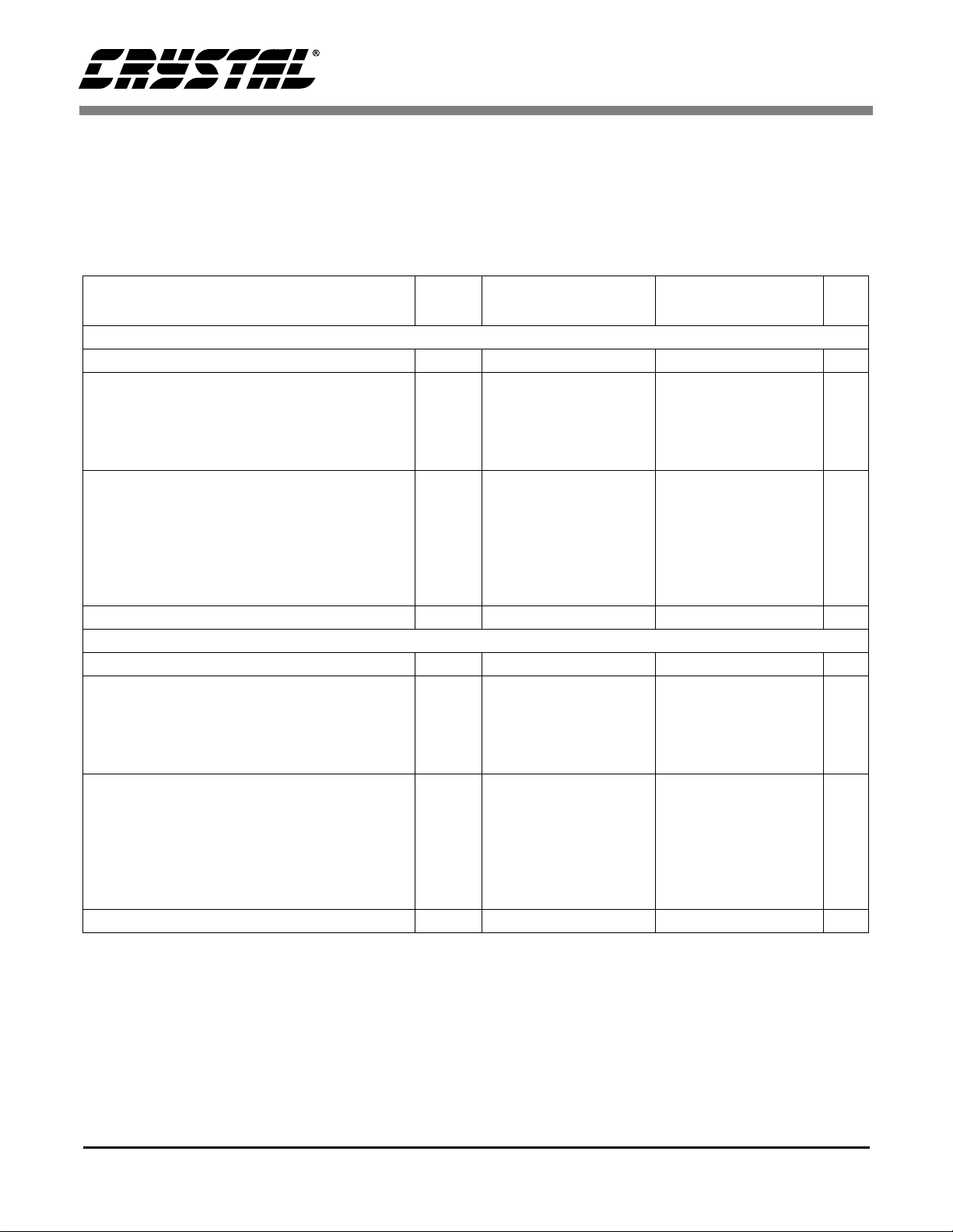
Parameters Symbol Min Typ Max Units
dc Accuracy
Interchannel Gain Mismatch - 0.1 0.4 dB
Gain Error - ±5 - %
Gain Drift - 100 - ppm/°C
Analog Output
Full Scale Output Voltage 3.25 3.5 3.75 Vpp
Quiescent Voltage V
Max AC-Load Resistance (Note 6) R
Max Load Capacitance (Note 6) C
Notes: 2. Filter response is not tested but is guaranteed by design.
3. Response is clock dependent and will scale with Fs. Note that the response plots (Figures 17-24) have
been normalized to Fs and can be de-normalized by multiplying the X-axis scale by Fs.
4. For Base-Rate Mode, the Measurement Bandwidth is 0.5465 Fs to 3 Fs.
For High-Rate Mode, the Measurement Bandwidth is 0.577 Fs to 1.4 Fs.
5. De-emphasis is not avai lab le in High - Rate Mod e.
6. Refer to Figure 2.
Q
L
L
-2.2-VDC
-3-k
- 100 - pF
Ω
DS248PP3 5
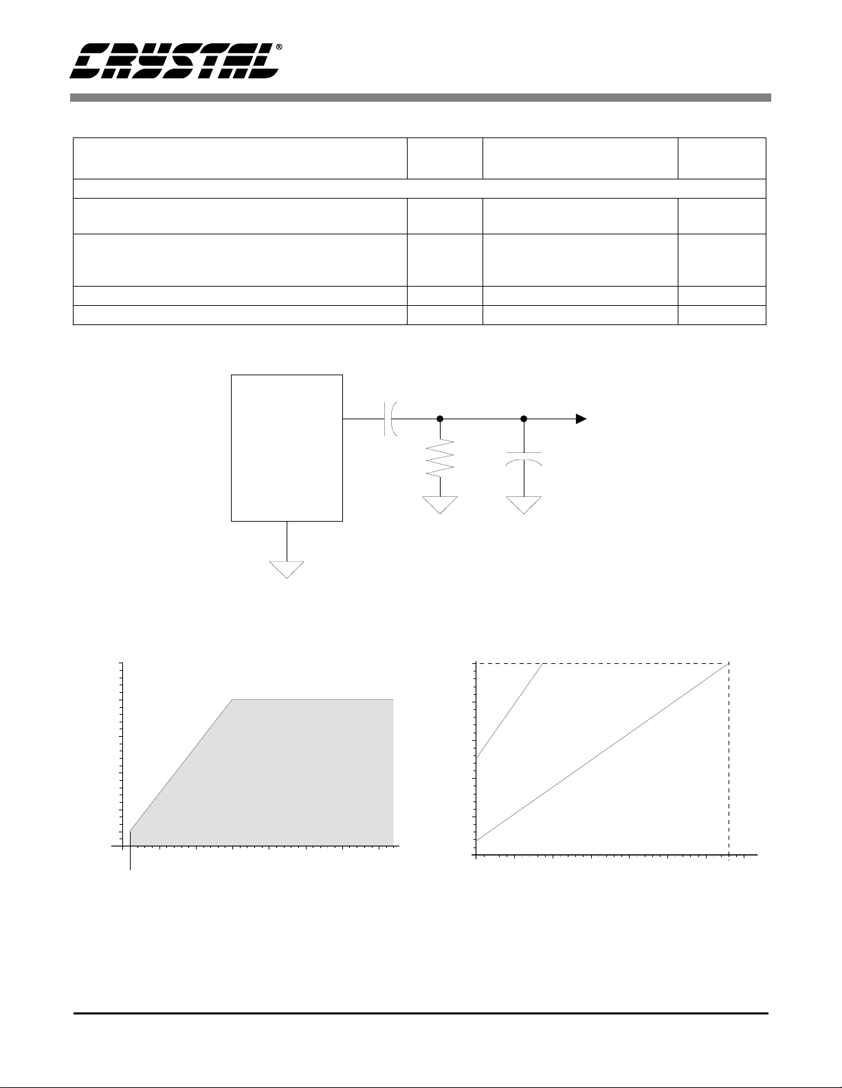
CS4334/5/6/7/8/9
100
50
75
25
2.5
51015
Safe Operating
Region
Capacitive Load -- C (pF)
L
Resistive Load -- R (kΩ)
L
125
3
20
Figure 2. Maximum Loading
POWER AND THERMAL CHARACTERISTICS
Parameters Symbol Min Typ Max Units
Power Supplies
Power Supply Current normal operation
power-down state
Power Dissipation (Note 7)
normal operation
power-down
Package Thermal Resistance
Power Supply Rejection Ratio (1 kHz) PSRR - 79 - dB
Notes: 7. Refer to Figure 3. Max Power Dissipation is measured at VA=5.5V.
10 µF
I
A
I
A
θ
JA
-
-
-
-
15
40
75
0.2
19
-
104
-
mA
µ
mW
mW
-110-°C/Watt
A
AGND
AOUTx
Figure 1. Output Test Load
V
out
R
L
75
70
65
60
Power (mW)
55
C
L
M
R
B
M
R
H
6 DS248PP3
50
30
40 50 60 70 80 90
Sample Rate (kHz)
Figure 3. Power vs. Sample Rate
100
CS4334/5/6/7/8/9
DIGITAL CHARACTERISTICS (T
= 25°C; VA = 4.75V - 5.5V)
A
Parameters Symbol Min Typ Max Units
High-Level Input Voltage V
Low-Level Input Voltage V
Input Leakage Current (Note 8) I
IH
IL
in
2.0 - - V
--0.8V
--±10µA
Input Capacitance - 8 - pF
Notes: 8. I
for CS433X LRCK is ±20µA max.
in
ABSOLUTE MAXIMUM RATINGS (AGND = 0V; all voltages with respect to ground.)
Parameters Symbol Min Max Units
DC Power Supply VA -0.3 6.0 V
Input Current, Any Pin Except Supplies I
Digital Input Voltage V
Ambient Operating Temperature (power applied) T
Storage Temperature T
in
IND
A
stg
-±10mA
-0.3 VA+0.4 V
-55 125 °C
-65 150 °C
WARNING: Operation at or beyond these limits may result in permanent damage to the device. Normal operation is
not guaranteed at these extremes.
RECOMMENDED OPERATING CONDITIONS (AGND = 0V; all voltages with respect to ground.)
Parameters Symbol Min Typ Max Units
DC Power Supply VA 4.75 5.0 5.5 V
DS248PP3 7

CS4334/5/6/7/8/9
()
()
SWITCHING CHARACTERISTICS (T
= -40 to 85°C; VA = 4.75V - 5.5V; Inputs: Logic 0 = 0V,
A
Logic 1 = VA, CL = 20pF)
Parameters Symbol Min Typ Max Units
Input Sample Rate Fs 2 - 100 kHz
MCLK Pulse Width High MCLK/LRCK = 512 10 - 1000 ns
MCLK Pulse Width Low MCLK/LRCK = 512 10 - 1000 ns
MCLK Pulse Width High MCLK / LRCK = 384 or 192 21 - 1000 ns
MCLK Pulse Width Low MCLK / LRCK = 384 or 192 21 - 1000 ns
MCLK Pulse Width High MCLK / LRCK = 256 or 128 31 - 1000 ns
MCLK Pulse Width Low MCLK / LRCK = 256 or 128 31 - 1000 ns
External SCLK Mode
LRCK Duty Cycle (External SCLK only) 40 50 60 %
SCLK Pulse Width Low t
SCLK Pulse Width High t
SCLK Period MCLK / LRCK = 512, 256 or 384 t
SCLK Period MCLK / LRCK = 128 or 192 t
SCLK rising to LRCK edge delay t
SCLK rising to LRCK edge setup time t
SDATA valid to SCLK rising setup time t
SCLK rising to SDATA hold time t
sclkl
sclkh
sclkw
sclkw
slrd
slrs
sdlrs
sdh
20 - - ns
20 - - ns
1
------------------- --128
1
------------------ 64
Fs
Fs
--ns
--ns
20 - - ns
20 - - ns
20 - - ns
20 - - ns
Internal SCLK Mode
LRCK Duty Cycle (Internal SCLK only) (Note 9) - 50 - %
SCLK Period (Note 10) t
SCLK rising to LRCK edge t
SDATA valid to SCLK rising setup time t
sclkw
sclkr
sdlrs
1
---------------- SCLK
--
1
------------------- --- 10+
()
512
Fs
--ns
tsclkw
----------------- 2
µ
--ns
s
SCLK rising to SDATA hold time
MCLK / LRCK = 512, 256 or 128
SCLK rising to SDATA hold time
MCLK / LRCK = 384 or 192
Notes: 9. In Internal SCLK Mode, the Duty Cycle must be 50%
t
sdh
t
sdh
1
------------------ ----15+
()
512
Fs
1
------------------ ----15+
()
384
Fs
+/−
1/2 MCLK Period.
--ns
--ns
10. The SCLK / LRCK ratio may be either 32, 48, or 64. This ratio depends on part type and MCLK/LRCK
ratio. (See figures 10-15)
8 DS248PP3
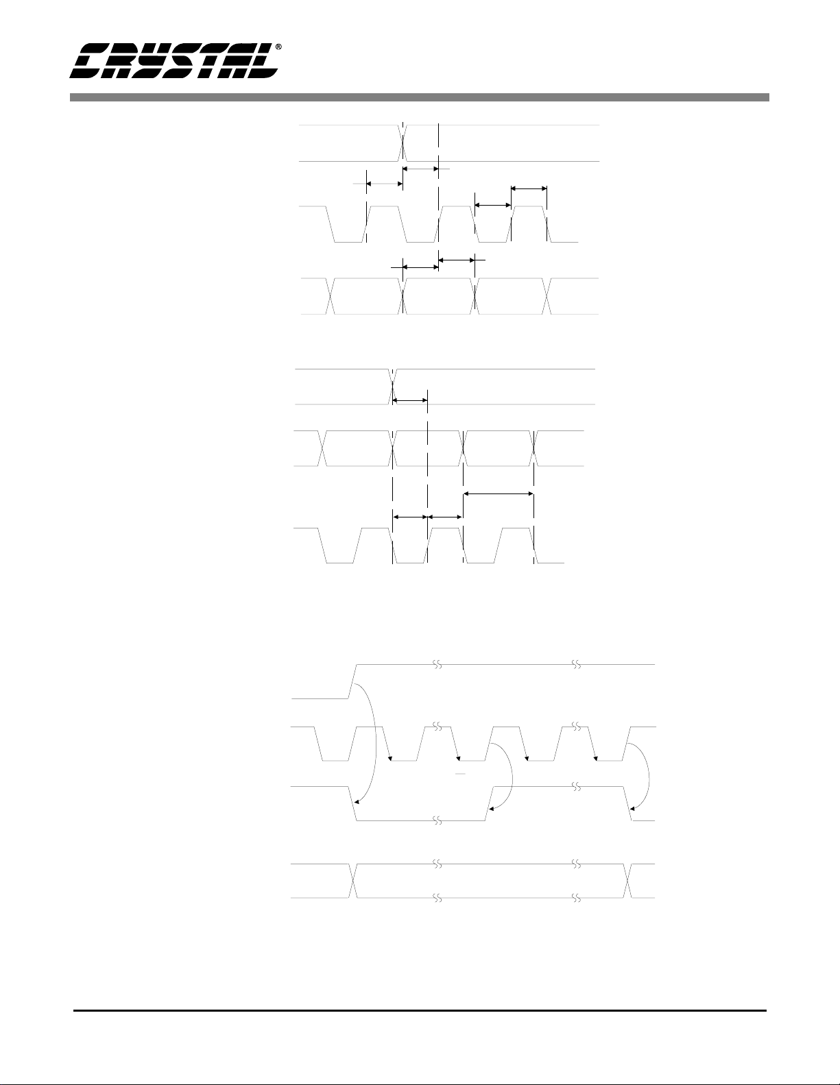
LRCK
SCLK
t
slrd
t
slrs
t
sclkl
t
sclkh
CS4334/5/6/7/8/9
t
sdh
SDATA
t
sdlrs
Figure 4. External Serial Mode Input Timing
LRCK
SDATA
*INTERNAL SCLK
t
sclkr
t
sdlrstsdh
t
sclkw
Figure 5. Internal Serial Mode Input Timing
* The SCLK pulses shown are internal to the CS4334/5/6/7/8/9.
LRCK
MCLK
*INTERNAL SCLK
SDATA
1
N
2
N
Figure 6. Internal Serial Clock Generation
* The SCLK pulses shown are internal to the CS4334/5/6/7/8/9.
N equals MCLK divided by SCLK
DS248PP3 9

2. TYPICAL CONNECTION DIAGRAM
CS4334/5/6/7/8/9
Audio
Data
Processor
External Clock
1
2
3
4
SDATA
DEM/SCLK
LRCK
CS4334
CS4335
CS4336
CS4337
CS4338
CS4339
MCLK
VA
7
0.1 µF
AOUTL
AOUTR
8
267 k
5
267 k
+
1 µF
3.3 µF
+
10 k
3.3 µF
+
10 k
+5V
560
Ω
Left Audio
Output
Ω
560
Ω
Ω
C
C
R
L
Right Audio
Output
R
L
R + 560
AGND
6
C =
L
4
Fs(R 560)
π
L
Figure 7. Recommended Connection Diagram
10 DS248PP3

CS4334/5/6/7/8/9
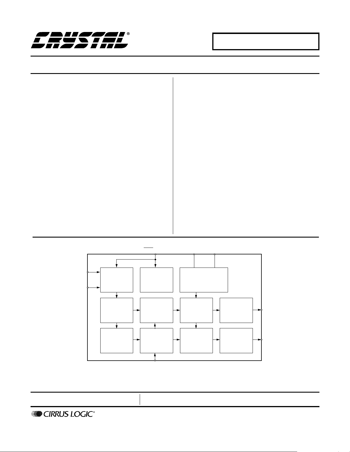
3. GENERAL DESCRIPTION
The CS4334 family of devices offers a complete
stereo digital-to-analog system including digital interpolation, fourth-order delta-sigma digital-to-analog conversion, digital de-emphasis and analog
filtering, as shown in Figure 8. This architecture
provides a high tolerance to clock jitter.
The primary purpose of using delta-sigma modulation techniques is to avoid the limitations of resistive laser trimmed digital-to-analog converter
architectures by using an inherently linear 1-bit
digital-to-analog converter. The advantages of a 1bit digital-to-analog converter include: ideal differential linearity, no distortion mechanisms due to resistor matching errors and no linearity drift over
time and temperature due to variations in resistor
values.
The CS4334 family of devices supports two modes
of operation. The devices operate in Base Rate
Mode (BRM) when MCLK/LRCK is 256, 384 or
512 and in High Rate Mode (HRM) when
MCLK/LRCK is 128 or 192. High Rate Mode allows input sample rates up to 100 kHz.
filter eliminates images of the baseband audio signal which exist at multiples of the input sample
rate. The resulting frequency spectrum has images
of the input signal at multiples of 4 Fs. These images are easily removed by the on-chip analog lowpass filter and a simple external analog filter (see
Figure 7).
3.2 Delta-Sigma Modulator
The interpolation filter is followed by a fourth order delta-sigma modulator which converts the interpolation filter output into 1-bit data at a rate of
128 Fs in BRM (or 64 Fs in HRM).
3.3 Switched-Capacitor DAC
The delta-sigma modulator is followed by a digitalto-analog converter which translates the 1-bit data
into a series of charge packets. The magnitude of
the charge in each packet is determined by sampling of a voltage reference onto a switched capacitor, where the polarity of each packet is controlled
by the 1-bit data. This technique greatly reduces the
sensitivity to clock jitter and provides low-pa ss filtering of the output.
3.1 Digital Interpolation Filter
The digital interpolation filter increases the sample
rate, Fs, by a factor of 4 and is followed by a
32× digital sample-and-hold (16× in HRM). This
Digital
Input
Interpolator
Delta-Sigma
Modulator
Figure 8. System Block Diagram
3.4 Analog Low-Pass Filter
The final signal stage consists of a continuous-time
low-pass filter which serves to smooth the output
and attenuate out-of-band noise.
DAC
Analog
Low-Pass
Filter
Analog
Output
DS248PP3 11

CS4334/5/6/7/8/9
4. SYSTEM DESIGN
The CS4334 family accepts data at standard audio
sample rates including 48, 44.1 and 32 kHz in
BRM and 96, 88.2 and 64 kHz in HRM. Audio data
is input via the serial data input pin (SDATA). The
Left/Right Clock (LRCK) defines the channel and
delineation of data, and the Serial Clock (SCLK)
clocks audio data into the input data buffer. The
CS4334/5/6/7/8/9 differ in serial data formats as
shown in Figures 10-15.
4.1 Master Clock
MCLK must be either 256x, 384x or 512x the de-
sired input sample rate in BRM and either 128x or
192x the desired input sample rate in HRM. The
LRCK frequency is equal to Fs, the frequency at
which words for each channel are input to the device. The MCLK-to-LRCK frequency ratio is detected automatically during the initialization
sequence by counting the number of MCLK transitions during a single LRCK period. Internal dividers are set to generate the proper clocks. Table 1
illustrates several standard audio sample rates and
the required MCLK and LRCK frequencies. Please
note there is no required phase relationship, but
MCLK, LRCK and SCLK must be synchronous.
4.2.1 External Serial Clock Mode
The CS4334 family will enter the External Serial
Clock Mode when 16 low to high transitions are
detected on the DEM/SCLK pin during any phase
of the LRCK period. When this mode is enabled,
the Internal Serial Clock Mode and de-emphasis
filter cannot be accessed. The CS4334 family will
switch to Internal Serial Clock Mode if no low to
high transitions are detected on the DEM/SCLK
pin for 2 consecutive frames of LRCK. Refer to
Figure 16.
4.2.2 Internal Serial Clock Mode
In the Internal Serial Clock Mode, the serial clock
is internally derived and synchronous with MCLK
and LRCK. The SCLK/LRCK frequency ratio is either 32, 48, or 64 depending upon data format. Operation in this mode is identical to operation with
an external serial clock synchronized with LRCK.
This mode allows access to the digital de-emphasis
function. Refer to Figures 10 - 16 for details.
While the Internal Serial Clock Mode is provided
to allow access to the de-emphasis filter, the Internal Serial Clock Mode also eliminates possible
clock interference from an external SCLK.
MCLK (MHz)
LRCK
(kHz)
32 4.0960 6.1440 8.1920 12.2880 16.3840
44.1 5.6448 8.4672 11.2896 16.9344 22.5792
48 6.1440 9.2160 12.2880 18.4320 24.5760
64 8.1920 12.2880 - - -
88.2 1 1.2896 16.9344 - - 96 12.2880 18.4320 - - -
HRM BRM
128x 192x 256x 384x 512x
4.3 De-Emphasis
The CS4334 family includes on-chip digital de-emphasis. Figure 9 shows the de-emphasis curve for
Fs equal to 44.1 kHz. The frequency response of
the de-emphasis curve will scale proportionally
with changes in sample rate, Fs.
The de-emphasis filter is active (inactive) if the
DEM/SCLK pin is low (high) for 5 consecutive
Table 1. Common Clock Frequencies
4.2 Serial Clock
The serial clock controls the shifting of data into
the input data buffers. The CS4334 family supports
both external and internal serial clock generation
modes. Refer to Figures 10-15 for data formats.
12 DS248PP3
falling edges of LRCK. This function is available
only in the internal serial clock mode.
4.4 Initialization and Power-Down
The Initialization and Power-Down sequence flow
chart is shown in Figure 16. The CS4334 family enters the Power-Down State upon initial power-up.

CS4334/5/6/7/8/9
Figure 9. De-Emphasis Curve (Fs = 44.1kHz)
Gain
dB
T1=50 µs
0dB
-10dB
F1 F2
3.183 kHz 10.61 kHz
T2 = 15 µs
Frequency
The interpolation filters and delta-sigma modulators are reset, and the internal voltage reference,
one-bit digital-to-analog converters and switchedcapacitor low-pass filters are powered down. The
device will remain in the Power-Down mode until
MCLK and LRCK are present. Once MCLK and
LRCK are detected, MCLK occurrences are counted over one LRCK period to determine the
MCLK/LRCK frequency ratio. Power is then applied to the internal voltage reference. Finally, power is applied to the D/A converters and switchedcapacitor filters, and the analog outputs will ramp to
the quiescent voltage, VQ.
4.5 Output Transient Control
capacitor to charge to VQ, effectively blocking the
quiescent DC voltage.
To prevent transients at power-down, the device
must first enter its power-down state. This is accomplished by removing MCLK or LRCK. When
this occurs, audio output ceases and the internal
output buffers are disconnected from AOUTL and
AOUTR. A soft-start current sink is substituted in
place of AOUTL and AOUTR which allows the
DC-blocking capacitors to slowly discharge. Once
this charge is dissipated, the power to the device
may be turned off, and the system is ready for the
next power-on.
To prevent an audio transient at the next power-on,
the DC-blocking capacitors must fully discharge
before turning off the power or exiting the powerdown state. If full discharge does not occur, a transient will occur when the audio outputs are initially
clamped to AGND. The time that the device must
remain in the power-down state is related to the
value of the DC-blocking capacitanc e. For example, with a 3.3 µF capacitor, the time that the de vice
must remain in the power-down state will be approximately 0.4 seconds.
The CS4334 family uses Popgaurd® technology to
minimize the effects of output transients during
power-up and power-down. This technique eliminates the audio transients commonly produced by
single-ended single-supply converters when it is
implemented with external DC-blocking capacitors
connected in series with the audio outputs. To
make best use of this feature, it is necessary to understand its operation.
When the device is initially powered-up, the audio
4.6 Grounding and Power Supply Decoupling
As with any high resolution converter, the CS4334
family requires careful attention to power supply
and grounding arrangements to optimize performance. Figure 7 shows the recommended power arrangement with VA connected to a clean +5V
supply. For best performance, decoupling capacitors should be located as close to the device pack-
age as possible with the smallest capacitor closest.
outputs, AOUTL and AOUTR, are clamped to
AGND. After a short delay of approximately 1000
sample periods, each output begins to ramp towards its quiescent voltage, VQ. Approximately
10,000 sample cycles later, the outputs reach V
and audio output begins. This gradual voltage
ramping allows time for the external DC-blocking
DS248PP3 13
4.7 Analog Output and Filtering
The analog filter present in the CS4334 family is a
switched-capacitor filter followed by a continuous
time low pass filter. Its response, combined with
Q
that of the digital interpolator, is given in Figures
17 - 24.

CS4334/5/6/7/8/9
LRCK
SCLK
SDATA +3 +2 +1
MSB
-1 -2 -3 -4 -5
Left Channel
+5 +4
Internal SCLK Mode External SCLK Mode
2
I
S, 16-Bit data and INT SCLK = 32 Fs if
MCLK/LRCK = 512, 256 or 128
2
I
S, Up to 24-Bit data and INT SCLK = 48 Fs if
MCLK/LRCK = 384 or 192
Figure 10. CS4334 Data Format (I2S)
LRCK
SCLK
SDATA +3 +2 +1
MSB
-1 -2 -3 -4 -5
Left Channel
+5 +4
LSB
LSB
Right Channel
+3 +2 +1
MSB
-1 -2 -3 -4
2
I
S, up to 24-Bit Data
+5 +4
Data Valid on Rising Edge of SCLK
Right Channel
+3 +2 +1
MSB
-1 -2 -3 -4
+5 +4
LSB
LSB
Internal SCLK Mode External SCLK Mode
Left Justified, up to 24-Bit Data
INT SCLK = 64 Fs if MCLK/LRCK = 512, 256 or 128
INT SCLK = 48 Fs if MCLK/L RCK = 384 or 192
Figure 11. CS4335 Data Format
LRCK
SCLK
SDATA
0
Left Channel
23 22 21 20 19 18
32 clocks
65432107
Internal SCLK Mode External SCLK Mode
Right Justified, 24-Bit Data
INT SCLK = 64 Fs if MCLK/LRCK = 512, 256 or 128
INT SCLK = 48 Fs if MCLK/L RCK = 384 or 192
Figure 12. CS4336 Data Format
Left Justified, up to 24-Bit Data
Data Valid on Rising Edge of SCLK
Right Channel
23 22 21 20 19 18
65432107
Right Justified, 24-Bit Data
Data Valid on Rising Edge of SCLK
SCLK Must Have at Least 48 Cycles per LRCK Period
14 DS248PP3

CS4334/5/6/7/8/9
LRCK
SCLK
SDATA
10 6543210987
17 16 17 16
19 18 19 18
Left Channel
15 14 13 12 11 10
32 clocks
6543210987
Internal SCLK Mode External SCLK Mode
Right Justified, 20-Bit Data
INT SCLK = 64 Fs if MCLK/LRCK = 512, 256 or 128
INT SCLK = 48 Fs if MCLK/L RCK = 384 or 192
Figure 13. CS4337 Data Format
LRCK
SCLK
SDATA
Left Channel
15 14 13 12 11 10
32 clocks
6543210987
Right Channel
15 14 13 12 11 10
Right Justified, 20-Bit Data
Data Valid on Rising Edge of SCLK
SCLK Must Have at Least 40 Cycles per LRCK Period
Right Channel
15 14 13 12 11 10
6543210987
Internal SCLK Mode External SCLK Mode
Right Justified, 16-Bit Data
INT SCLK = 32 Fs if MCLK/LRCK = 512, 256 or 128
INT SCLK = 48 Fs if MCLK/L RCK = 384 or 192
Figure 14. CS4338 Data Format
LRCK
SCLK
SDATA
10
17 16 17 16
Left Channel
15 14 13 12 11 10
32 clocks
6543210987
Internal SCLK Mode External SCLK Mode
Right Justified, 18-Bit Data
INT SCLK = 64 Fs if MCLK/LRCK = 512, 256 or 128
INT SCLK = 48 Fs if MCLK/L RCK = 384 or 192
Figure 15. CS4339 Data Format
Right Justified, 16-Bit Data
Data Valid on Rising Edge of SCLK
SCLK Must Have at Least 32 Cycles per LRCK Period
Right Channel
15 14 13 12 11 10
6543210987
Right Justified, 18-Bit Data
Data Valid on Rising Edge of SCLK
SCLK Must Have at Least 36 Cycles per LRCK Period
DS248PP3 15

CS4334/5/6/7/8/9
Figure 16. CS4334/5/6/7/8/9 Initialization and Power-Down Sequence
16 DS248PP3

4.8 Overall Base-Rate Frequency Response
Figure 17. Stopband Rejection Figure 18. Transition Band
CS4334/5/6/7/8/9
0.1
0.08
0.06
0.04
Amplitude dB
0.02
0
0.02
0 0.05 0.1 0.15 0.2 0.25 0.3 0.35 0.4 0.45
Frequency (normalized to Fs)
Figure 19. Transition Band Figure 20. Passband Ripple
DS248PP3 17

4.9 Overall High-Rate Frequency Response
Figure 21. Stopband Rejection Figure 22. Transition Band
CS4334/5/6/7/8/9
0.25
0.2
0.15
0.1
0.05
Amplitude dB
0
0.05
0.1
0.15
0 0.05 0.1 0.15 0.2 0.25 0.3 0.35 0.4 0.45
Frequency (normalized to Fs)
Figure 23. Transition Band Figure 24. Passband Ripple
18 DS248PP3
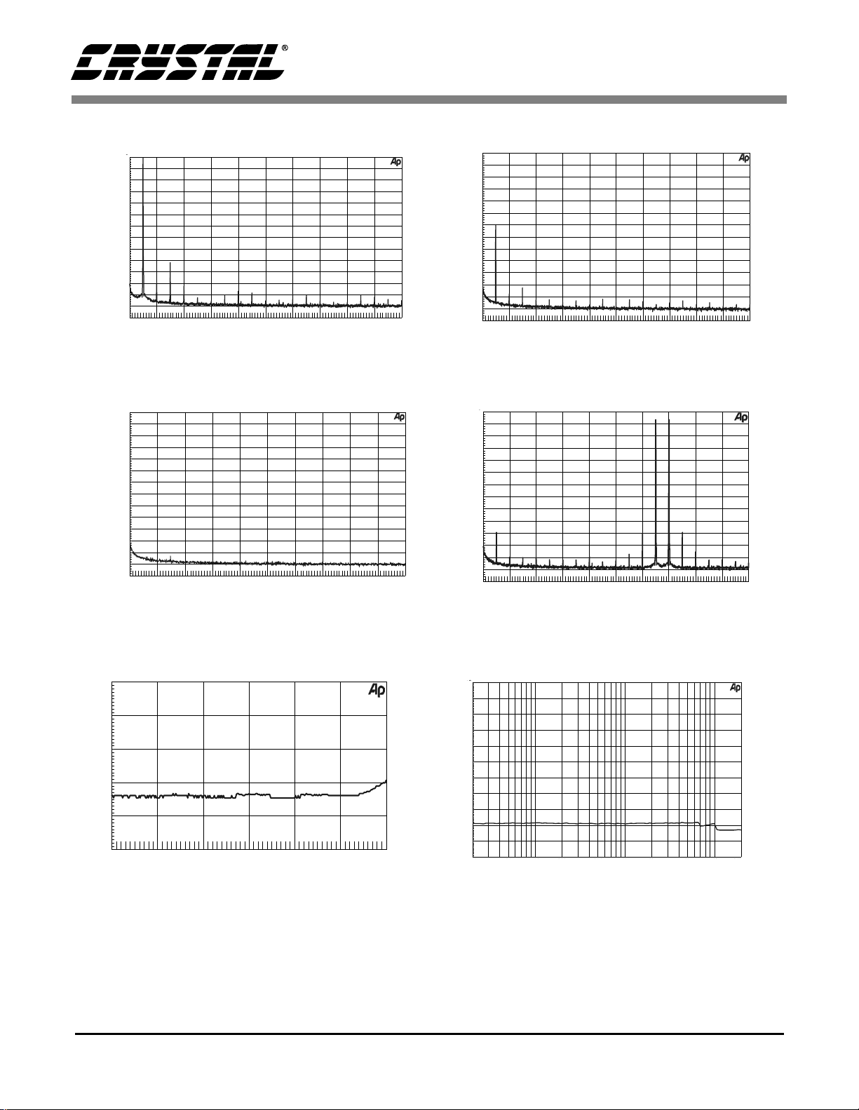
4.10 Base Rate Mode Performance Plots
+0
+0
+0
-110
-60
-100
-90
-80
-70
d
B
r
A
-60 +0-50 -40 -30 -20 -10
dBFS
-50 -40 -30 -20 -10
dBFS
-60 +0
-110
-100
-90
-80
-70
-60
dBr A
+0
+0
+0
-10
-10
-10
-20
-20
-20
-30
-30
-30
-40
-40
-40
-50
-50
-50
-60
-60
-60
d
B
-70
r
-70
dBr A
-70
dBr A
A
-80
-80
-80
-90
-90
-90
-100
-100
-100
-110
-110
-110
-120
-120
-120
-130
-130
-130
-140
-140
-140
2k 20k4k 6k 8k 10k 12k 14k 16k 18k
4k 6k 8k 10k 12k 14k 16k 18k
2k
2k 6k4k 8k 10k 12k 14k 16k 18k 20k
(16k FFT of a 1 kHz input signal)
Figure 25. 0 dBFS FFT (BRM)
Hz
Hz
Hz
CS4334/5/6/7/8/9
+0
+0
-10
-10
-10
-20
-20
-20
-30
-30
-30
-40
-40
-40
-50
-50
-50
-60
-60
-60
d
B
-70
r
-70
-70
dBr A
dBr A
A
-80
-80
-80
-90
-90
-90
-100
-100
-100
-110
-110
-110
-120
-120
-120
-130
-130
-130
-140
-140
20k
20k
-140
2k 20k4k 6k 8k 10k 12k 14k 16k 18k
4k 6k 8k 10k 12k 14k 16k 18k
2k
2k 6k4k 8k 10k 12k 14k 16k 18k
Hz
Hz
Hz
(16k FFT of a 1 kHz input signal)
Figure 26. -60 dBFS FFT (BRM)
20k
20k
+0
+0
+0
-10
-10
-10
-20
-20
-20
-30
-30
-30
-40
-40
-40
-50
-50
-50
-60
-60
-60
d
B
-70
r
-70
dBr A
-70
dBr A
A
-80
-80
-80
-90
-90
-90
-100
-100
-100
-110
-110
-110
-120
-120
-120
-130
-130
-130
-140
-140
-140
2k 20k4k 6k 8k 10k 12k 14k 16k 18k
4k 6k 8k 10k 12k 14k 16k 18k
2k
2k 6k4k 8k 10k 12k 14k 16k 18k
Hz
Hz
Hz
20k
20k
(16k FFT with no input signal)
Figure 27. Idle Channel Noise FFT (BRM)
(THD+N plots measured using a 1kHz 24-bit dithered input signal)
Figure 29. THD+N vs. Amplitude (BRM)
+0
+0
-10
-10
-10
-20
-20
-20
-30
-30
-30
-40
-40
-40
-50
-50
-50
-60
-60
-60
d
B
-70
r
-70
dBr A
-70
dBr A
A
-80
-80
-80
-90
-90
-90
-100
-100
-100
-110
-110
-110
-120
-120
-120
-130
-130
-130
-140
-140
-140
2k 20k4k 6k 8k 10k 12k 14k 16k 18k
4k 6k 8k 10k 12k 14k 16k 18k
2k
2k 6k4k 8k 10k 12k 14k 16k 18k
Hz
Hz
Hz
20k
20k
(16k FFT of intermodulation distortion using 13 kHz and 14 kHz input signals)
Figure 28. Twin Tone IMD FFT (BRM)
+0
+0
-10
-10
-10
-20
-20
-20
-30
-30
-30
-40
-40
-40
A
d
-50
-50
r
-50
B
B
r
d
-60
-60
dBr A
-60
A
-70
-70
-70
-80
-80
-80
-90
-90
-90
-100
-100
-100
-110
-110
-110
20 20k50 100 200 500 1k 2k 5k 10k
20 50 100
50 200 500 1k 2k 5k 10k
20 20k
100
200
500 1k 2k 5k 10k 20k
Hz
Hz
Hz
(THD+N plots measured using a 1kHz 24-bit dithered input signal)
Figure 30. THD+N vs. Frequency (BRM)
All measurements were taken from the CDB4334 evaluation board using the Audio Precision Dual Domain
DS248PP3 19
System Two Cascade.
4.11 High Rate Mode Performance Plots
+0
+0
+0
Audio P
08/05/99 11:11:36D-A CCIF IMD
AMPLITUDE
-60
+0
+0
+0
-10
-10
-10
-20
-20
-20
-30
-30
-30
-40
-40
-40
-50
-50
-50
-60
-60
-60
d
B
-70
r
-70
-70
dBr A
dBr A
A
-80
-80
-80
-90
-90
-90
-100
-100
-100
-110
-110
-110
-120
-120
-120
-130
-130
-130
-140
-140
-140
2k 20k4k 6k 8k 10k 12k 14k 16k 18k
4k 6k 8k 10k 12k 14k 16k 18k
2k
2k 6k4k 8k 10k 12k 14k 16k 18k
(16k FFT of a 1 kHz input signal)
Figure 31. 0 dBFS FFT (HRM)
Hz
Hz
Hz
20k
CS4334/5/6/7/8/9
+0
+0
-10
-10
-10
-20
-20
-20
-30
-30
-30
-40
-40
-40
-50
-50
-50
-60
-60
-60
d
B
-70
r
-70
-70
dBr A
dBr A
A
-80
-80
-80
-90
-90
-90
-100
-100
-100
-110
-110
-110
-120
-120
-120
-130
-130
-130
-140
-140
-140
2k 20k4k 6k 8k 10k 12k 14k 16k 18k
4k 6k 8k 10k 12k 14k 16k 18k
2k
20k
2k 6k4k 8k 10k 12k 14k 16k 18k
(16k FFT of a 1 kHz input signal)
Hz
Hz
Hz
Figure 32. -60 dBFS FFT (HRM)
20k
20k
+0
+0
-10
-10
-10
-20
-20
-20
-30
-30
-30
-40
-40
-40
-50
-50
-50
-60
-60
-60
d
B
-70
r
-70
-70
dBr A
dBr A
A
-80
-80
-80
-90
-90
-90
-100
-100
-100
-110
-110
-110
-120
-120
-120
-130
-130
-130
-140
-140
-140
2k 20k4k 6k 8k 10k 12k 14k 16k 18k
4k 6k 8k 10k 12k 14k 16k 18k
2k 6k4k 8k
2k
12k 14k 16k 18k
10k
Hz
Hz
Hz
(16k FFT with no input signal)
Figure 33. Idle Channel Noise FFT (HRM)
-60
-70
-70
-80
d
-80
B
r
dBr A
A
-90
-90
-100
-100
-110
-110
-60 +0-50 -40 -30 -20 -10
-60 +0
(THD+N plots measured using a 1kHz 24-bit dithered input signal)
-50 -40 -30 -20 -10
Figure 35. THD+N vs. Amplitude (HRM)
dBFS
dBFS
20k
20k
recision
+0
+0
+0
-10
-10
-10
-20
-20
-20
-30
-30
-30
-40
-40
-40
-50
-50
-50
-60
d
-60
-60
B
-70
r
-70
-70
dBr A
dBr A
-80
A
-80
-80
-90
-90
-90
-100
-100
-100
-110
-110
-110
-120
-120
-120
-130
-130
-130
-140
-140
-140
2k 20k4k 6k 8k 10k 12k 14k 16k 18k
4k 6k 8k 10k 12k 14k 16k 18k
2k
2k 6k4k 8k 10k 12k 14k 16k 18k
(16k FFT of intermodulation distortion using 13 kHz and 14 kHz input signals)
vs
20k
Hz
Hz
Hz
20k
Figure 34. Twin Tone IMD FFT (HRM)
+0
+0
-10
-10
-10
-20
-20
-20
-30
-30
-30
-40
-40
-40
d
A
-50
B
-50
r
-50
B
r
d
-60
-60
dBr A
-60
A
-70
-70
-70
-80
-80
-80
-90
-90
-90
-100
-100
-100
-110
-110
-110
20 20k50 100 200 500 1k 2k 5k 10k
20 50 100
20 20k
50 200
100
200
500 1k 2k 5k 10k 20k
500
1k 2k
Hz
Hz
Hz
5k 10k
(THD+N plots measured using a 1kHz 24-bit dithered input signal)
Figure 36. THD+N vs. Frequency (HRM)
All measurements were taken from the CDB4334 evaluation board using the Audio Precision Dual Domain
System Two Cascade.
20 DS248PP3

5. PIN DESCRIPTIONS
CS4334/5/6/7/8/9
SERIAL DATA INPUT SDATA AOUTL ANALOG LEFT CHANNEL OUTPUT
DE-EMPHASIS / SCLK DEM/SCLK VA ANALOG POWER
LEFT / RIGHT CLOCK LRCK AGND ANALOG GROUND
MASTER CLOCK MCLK AOUTR ANALOG RIGHT CHANNEL OUTPUT
No. Pin Name I/O Pin Function and Description
1SDATAI
2DEM/SCLKI
3 LRCK I
4MCLKI
5AOUTRO
6AGNDI
7VAI
8AOUTLO
Serial Audio Data Input
The data is clocked into the CS4334/5/6/7/8/9 via internal or external SCLK, and the
channel is determined by LRCK.
De-Emphasis/External Serial Clock Input
nal serial clock input.
Left/Right Clock
Data Input pin, SDATA.
Master Clock
either 128x or 192x the input sample rate in HRM.
Analog Right Channel Output
Analog Ground
Analog Power
Analog Left Channel Output
- determines which channel is currently being input on the Audio Serial
- frequency must be 256x, 384x, or 512x the input sample rate in BRM and
- analog ground reference is 0V.
- analog power supply is nominally +5V.
- two’s complement MSB-first serial data is input on this pin.
81
72
63
54
- used for de-emphasis filter control or exter-
- typically 3.5 Vp-p for a full-scale input signal.
- typically 3.5 Vp-p for a full-scale input signal.
DS248PP3 21
6. PARAMETER DEFINITIONS
Tot al Harmonic Distortion + Noise (THD+N)- The ratio of the rms value of the signal to the
rms sum of all other spectral components over the specified bandwidth (typically 10Hz to
20kHz), including distortion components. Expressed in decibels.
Dynamic Range - The ratio of the full scale rms value of the signal to the rms sum of all other
spectral components over the specified bandwidth. Dynamic range is a signal-to-noise
measurement over the specified bandwidth made with a -60 dBFS signal. 60 dB is then added
to the resulting measurement to refer the measurement to full scale. This technique ensures that
the distortion components are below the noise level and do not effect the measurement. This
measurement technique has been accepted by the Audio Engineering Society, AES17-1991, and
the Electronic Industries Association of Japan, EIAJ CP-307.
Interchannel Isolation - A measure of crosstalk between the left and right channels. Measured
for each channel at the converter’s output with all zeros to the input under test and a full-scale
signal applied to the other channel. Units in decibels.
Interchannel Gain Mismatch - The gain difference between left and right channels. Units in
decibels.
CS4334/5/6/7/8/9
Gain Error - The deviation from the nominal full scale analog output for a full scale digital
input.
Gain Drift - The change in gain value with temperature. Units in ppm/°C.
7. REFERENCES
1) "How to Achieve Optimum Performance from
Delta-Sigma A/D & D/A Converters" by
Steven Harris. Paper presented at the 93rd Convention of the Audio Engineering Society, October 1992.
2) CDB4334/5/6/7/8/9 Evaluation Board Datasheet
22 DS248PP3
8. ORDERING INFORMATION:
Model Temperature Package Serial Interface
CS4334-KS -10 to +70 °C 8-pin Plastic SOIC 16 to 24-bit, I2S
CS4335-KS -10 to +70 °C 8-pin Plastic SOIC 16 to 24-bit, left justified
CS4336-KS -10 to +70 °C 8-pin Plastic SOIC 24-bit, right justified
CS4337-KS -10 to +70 °C 8-pin Plastic SOIC 20-bit, right justified
CS4338-KS -10 to +70 °C 8-pin Plastic SOIC 16-bit, right justified
CS4339-KS -10 to +70 °C 8-pin Plastic SOIC 18-bit, right justified, 32 F
CS4334-BS -40 to +85 °C 8-pin Plastic SOIC 16 to 24-bit, I2S
CS4335-BS -40 to +85 °C 8-pin Plastic SOIC 16 to 24-bit, left justified
CS4336-BS -40 to +85 °C 8-pin Plastic SOIC 24-bit, right justified
CS4337-BS -40 to +85 °C 8-pin Plastic SOIC 20-bit, right justified
CS4338-BS -40 to +85 °C 8-pin Plastic SOIC 16-bit, right justified
CS4339-BS -40 to +85 °C 8-pin Plastic SOIC 18-bit, right justified, 32 F
9. FUNCTIONAL COMPATIBILITY
CS4330-KS ⇒ CS4339-KS
CS4334/5/6/7/8/9
Internal SCLK mode
s
Internal SCLK mode
s
CS4331-KS ⇒ CS4334-KS
CS4333-KS ⇒ CS4338-KS
CS4330-BS ⇒ CS4339-BS
CS4331-BS ⇒ CS4334-BS
CS4333-BS ⇒ CS4338-BS
DS248PP3 23
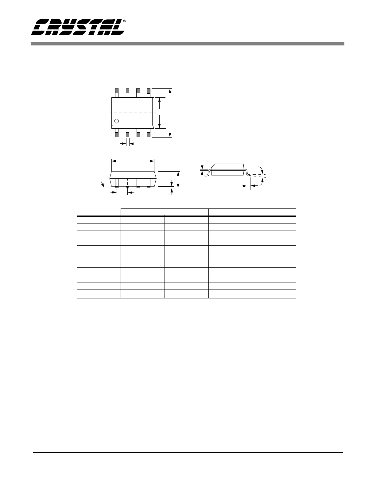
10. PACKAGE DIMENSIONS
8L SOIC (150 MIL BODY) PACKAGE DRAWING
1
b
CS4334/5/6/7/8/9
E
H
c
L
SEATING
PLANE
D
A
e
A1
INCHES MILLIMETERS
DIM MIN MAX MIN MAX
A 0.053 0.069 1.35 1.75
A1 0.004 0.010 0.10 0.25
B 0.013 0.020 0.33 0.51
C 0.007 0.010 0.19 0.25
D 0.189 0.197 4.80 5.00
E 0.150 0.157 3.80 4.00
e 0.040 0.060 1.02 1.52
H 0.228 0.244 5.80 6.20
L 0.016 0.050 0.40 1.27
∝
0° 8° 0° 8°
JEDEC # : MS-012
∝
24 DS248PP3

• Notes •

 Loading...