

CS4329
20-Bit, Stereo D/A Converter for Digital Audio
Features
l
20-Bit Conversion
l
115 dB Signal-to-Noise-Ratio (EIAJ)
l
Complete Stereo DAC System
- 128X Interpolation Filter
- Delta-Sigma DAC
- Analog Post Filter
l
106 dB Dynamic Range
l
Low Clock Jitter Sensitivity
l
Filtered Line-Level Outputs
- Linear Phase Filtering
- Zero Phase Error Between Channels
l
Adjustable System Sampling Rates
- including 32 kHz, 44.1 kHz & 48 kHz
l
Digital De-emphasis for 32 kHz, 44.1 kHz, &
48 kHz
l
Pin-compatible with the CS4390
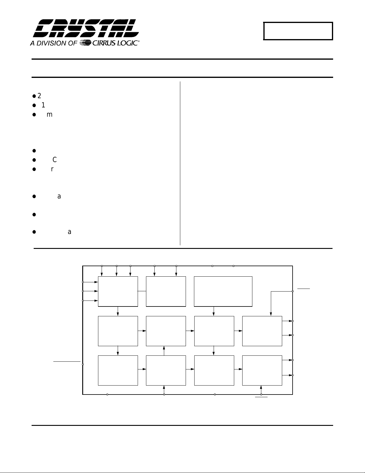
I
Description
The CS4329 is a complete stereo digital-to-analog output system. In addit ion to the tr aditional D/A function, t he
CS4329 includes a digital interpolation filter followed by
an 128X oversampled delt a-sigma modulator. The modulator output controls the reference voltage input to an
ultra-linear analog low-pass filter. This architecture allows for infin ite adjustment of sample rate between 1 and
50 kHz while maintaining linear phase response simply
by changing the master clock frequency.
The CS4329 also includes an extremely flexible serial
port utilizing mode select pins to support multiple interface formats.
The master clock can be either 256, 384, or 512 times
the input sample rate, supporting various audio
environments.
ORDERING INFORMATION
CS4329-KP -10° to 70° C 20-pin Plastic DIP
CS4329-KS -10° to 70° C 20-pin Plastic SSOP
CDB4329 Evaluation Board
DIF0
DIF1
DIF2
20
19
12 3 6
10
7
9
11
Serial Input
Interface
Interpolator
Interpolator
5
DGND
LRCK
SCLK
SDATA
AUTO_MUTE
Cirrus Logic, Inc.
Crystal Semiconductor Products Division
P.O. Box 17847, Austin, Texas 78760
(512) 445 7222 FAX: (512) 445 7581
http://www.crystal.com
DEM01DEM1
De-emphasis
Delta-Sigma
Modulator
Delta-Sigma
Modulator
8
MCLK
VA VD
2
Voltage Reference
DAC
DAC
4
AGND
Copyright Cirrus Logic, Inc. 1998
(All Rights Reserved)
Analog
Low-Pass
Filter
Analog
Low-Pass
Filter
15
MUTE_R
MUTE_L
16
AOUTL+
18
AOUTL-
17
AOUTR+
14
AOUTR-
13
APR ‘98
DS153F1
1
CS4329
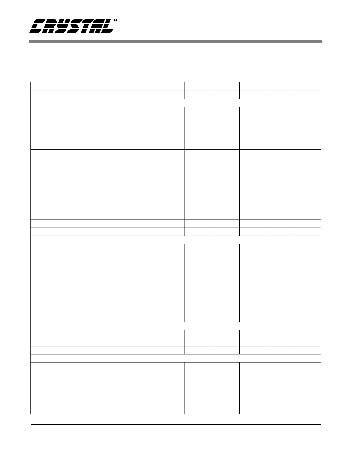
ANALOG CHARACTERISTICS (T
48 kHz; Input Data = 20 Bits; SCLK = 3.072 MHz; MCLK = 12.288 MHz; R
= 25°C; Full-Scale Differential Output Sine wave, 997 Hz; Fs =
A
= 20 kΩ differential; VD = VA = 5 V;
L
Logic "1" = VD; Logic "0" = DGND; Measurement Bandwidth is 10 Hz to 20 kHz, unweighted unless otherwise
specified.)
Parameter Symbol Min Typ Max Unit
Specified Temperature Operating Range T
A
-10 - 70 °C
Dynamic Performance
Dynamic Range 20-Bit (Note 1)
(A-Weighted)
18-Bit
(A-Weighted)
16-Bit
(A-Weighted)
Total Harmonic Distortion + Noise (Note 1)
20-Bit 0 dB
-20 dB
-60 dB
18-Bit 0 dB
-20 dB
-60 dB
16-Bit 0 dB
-20 dB
-60 dB
THD+N
98
101
-
-
-
-
-90
-78
-38
-
-
-
-
-
-
103
106
101
104
94
96
-97
-83
-43
-96
-81
-41
-93
-74
-34
-
-
-
-
-
-
-
-
-
-
-
-
-
-
-
dB
dB
dB
dB
dB
dB
dB
dB
dB
dB
dB
dB
dB
dB
dB
Idle Channel Noise / Signal-to-Noise-Ratio (Note 2) - 115 - dBFS
Interchannel Isolation (1 kHz) - -110 - dB
Combined Digital and Analog Filter Characteristics
Frequency Response 10 Hz to 20 kHz (Note 3) - ±0.1 - dB
Deviation from linear phase - ±0.5 - deg
Passband: to -0.1 dB corner (Note 3) 0 - 21.77 kHz
Passband Ripple - - ±0.001 dB
StopBand (Note 3) 26.23 - - kHz
StopBand Attenuation (Note 3) 75 - - dB
Group Delay (Note 4) - 25/Fs - s
De-emphasis Error (referenced to 1 kHz) Fs = 32 kHz
Fs = 44.1 kHz
Fs = 48 kHz
-
-
-
-
-
-
+0.3/-0.3
+0.2/-0.4
+0.1/-0.45
dB
dB
dB
dc Accuracy
Interchannel Gain Mismatch - 0.1 - dB
Ga in E rror - ±2 ±5 %
Gain Drift - 200 - ppm/°C
Power Supplies
Power Supply Current: Normal Operation
Power-down
Power Dissipation Normal Operation
Power-down
I
I
IA+I
A
D
D
-
-
-
-
-
-
30
12
42
500
185
2.5
-
-
45
-
22.5
-
mA
mA
mA
µA
mW
mW
Power Supply Rejection Ratio (1 kHz) PSRR - 60 - dB
2 DS153F1
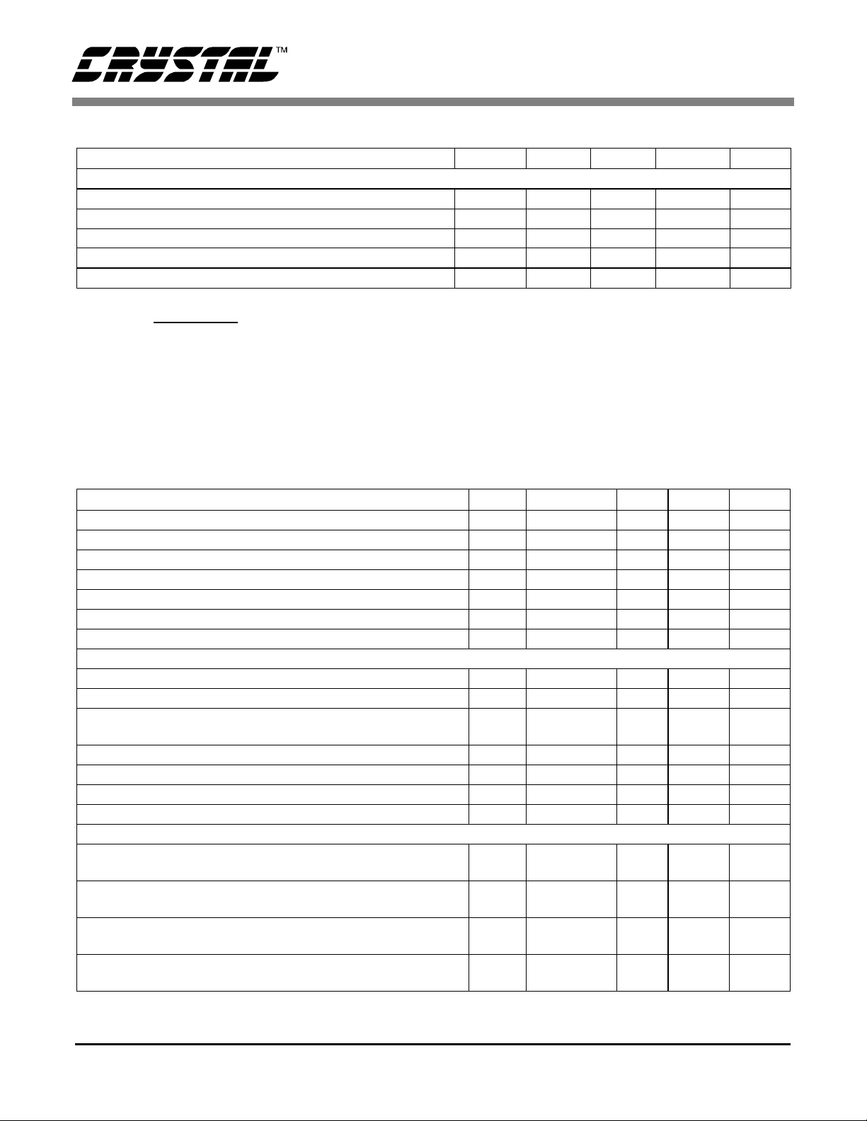
CS4329
ANALOG CHARACTERISTICS (CONTINUED)
Parameter Symbol Min Typ Max Unit
Analog Output
Differential Full Scale Output Voltage (Note 5) 1.90 2.0 2.10 Vrms
Output Common Mode Voltage - 2.2 - V
Differentia l Offs et - 3 15 mV
AC Load Resistance R
Load Capacitance C
Notes: 1. Triangular PDF Dithered Data
2. AUTO-MUTE
active. See parameter definitions
3. The passband and stopband edges scale with frequency. For input sample rates, Fs, other than 48 kHz,
the passband edge is 0.4535×Fs and the stopband edge is 0.5465×Fs.
4. Group Delay for Fs=48 kHz 25/48 kHz=520µs
5. Specified for a fully differential output ±((AOUT+)-(AOUT-)). See Figure 12.
L
L
4- -k
- - 100 pf
Ω
SWITCHING CHARACTERISTICS
to 4.75 Volts; C
=20pF)
L
(TA= -10 to 70°C; Logic 0 = AGND = DGND; Logic 1 = VD = VA = 5.25
Parameter Symbol Min Typ Max Unit
Input Sample Rate Fs 1 - 50 kHz
MCLK Pulse Width High MCLK / LRCK = 512 10 - - ns
MCLK Pulse Width Low MCLK / LRCK = 512 10 - - ns
MCLK Pulse Width High MCLK / LRCK = 384 21 - - ns
MCLK Pulse Width Low MCLK / LRCK = 384 21 - - ns
MCLK Pulse Width High MCLK / LRCK = 256 31 - - ns
MCLK Pulse Width Low MCLK / LRCK = 256 32 - - ns
External SCLK Mode
SCLK Pulse Width Low t
SCLK Pulse Width High t
SCLK Period t
SCLK rising to LRCK edge delay t
SCLK rising to LRCK edge setup time t
SDATA valid to SCLK rising setup time t
SCLK rising to SDATA hold time t
sclkl
sclkh
sclkw
slrd
slrs
sdlrs
sdh
20 --ns
20 --ns
1
-------------------128 Fs()
--ns
20 --ns
20 --ns
20 --ns
20 --ns
Internal SCLK Mode
SCLK Period SCLK / LRCK = 64 t
SDATA valid to SCLK rising setup time t
SCLK rising to SDATA hold time MCLK / LRCK = 256 or 512 t
SCLK rising to SDATA hold time MCLK / LRCK = 384 t
sclkw
sdlrs
sdh
sdh
1
----------------64 Fs()
1
-------------------512 Fs()
1
-------------------512 Fs()
1
-------------------384 Fs()
--ns
10+
15+
15+
--ns
--ns
--ns
DS153F1 3
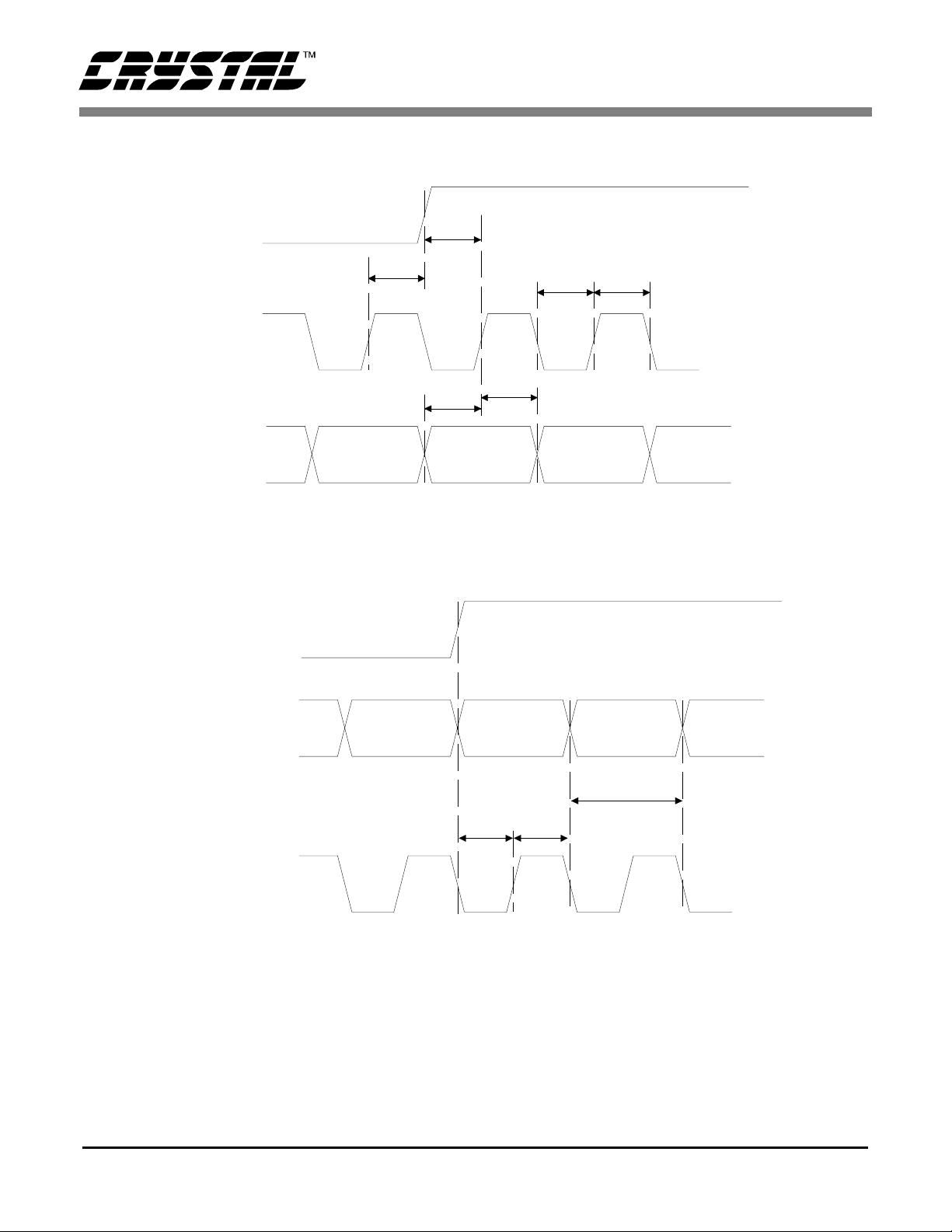
LRCK
SCLK
SDATA
t
slrs
t
slrd
t
sdlrs
External Serial Mode Input Timing
t
t
sclkl
sdh
t
sclkh
CS4329
LRCK
SDATA
*INTERNA L SCLK
* The SCLK pin must be terminated to ground.
The SCLK pulses shown are internal to the CS4329.
sdlrstsdh
Internal Serial Mode Input Timing
t
t
sclkw
4 DS153F1
CS4329
DIGITAL CHARACTERISTICS (T
Parameter Symbol Min Typ Max Unit
High-Level Input Voltage V
Low-Level Input Voltage V
Input Leakage Current V
Digital Input Capacitance - 10 - pF
= 25°C; VD = 5 V ±5%)
A
IH
IL
in
2.0 - - V
--0.8V
--±10.0
µ
A
ABSOLUTE MAXIMUM RATINGS (AGND = 0 V, all voltages with respect to ground.)
Parameter Symbol Min Max Unit
DC Power Supply: Positive Analog
Positi ve D ig ital
|VA - VD|
Input Current, Any Pin Except Supplies I
Digital Input Voltage V
Ambient Operating Temperature (power applied) T
Storage Temperature T
WARNING: Operation at or beyond these limits may result in permanent damage to t he device.No rmal operat ion is
not guaranteed at these extremes.
RECOMMENDED OPERATING CONDITIONS
VA
VD
in
IND
A
stg
(DGND = 0V; all voltages with respect to ground)
-0.3
-0.3
0.0
-±10mA
-0.3 (VD)+0.4 V
-55 125 °C
-65 150 °C
6.0
6.0
0.4
V
V
V
Parameter Symbol Min Typ Max Unit
DC Power Supply: Positive Digital
Positi ve Analog
|VA - VD|
VD
VA
4.75
4.75
-
5.0
5.0
-
5.25
5.25
0.4
V
V
V
DS153F1 5
CS4329
Ω
10
1 µF
+
0.1 µF
+
1 µF
0.1 µF
+5V
Analog
Mode
Select
Audio
Data
Processor
External Clock
20
DIF0
19
DIF1
12
DIF2
7
LRCK
9
SCLK*
10
SDATA
1
DEM0
2
DEM1
15
MUTE_R
16
MUTE_L
11
AUTO_MUTE
8
MCLK
VD
6
DGND
CS4329
AGND
5
3
VA
AOUTL-
AOUTL+
AOUTR-
AOUTR+
4
17
Analog
Conditioning
18
13
Analog
Conditioning
14
* SCLK mus t be connec ted to D GND
for operation in Internal SCLK Mode
Figure 1. Typical Connection Diagram
6 DS153F1
CS4329
GENERAL DESCRIPTION
The CS4329 is a com plete ste reo dig ital-t o-analo g
system including 128× digital interpolation, fourthorder delta-sigma digital-to-analog conversion,
128× oversampled one-bit delta-sigma modulator
and analog filtering. This architecture provides a
high insensitivity to clock jitter. The DAC converts
digital data at a ny input sample rat e bet w een 1 and
50 kHz, including the standa rd audio rates of 48,
44.1 and 32 kHz.
The primary purpose of using delta-sigma modula-
tion techni ques is to avo id the limi tations of lase r
trimmed resistive DAC architectures by using an
inherently linear 1-bit DAC. The advantages of a 1bit DAC include: ideal differential linearity, no distortion mechanisms due to resistor matching errors
and no linearity drift over time and temperature due
to variations in resist or va lues.
Digital Interpolation Filter
The digital interpolation filter increases the sample
rate by a factor of 4 and is followed by a 32× digital
sample-and hold to effectivel y achieve a 128× interpolation filter. This filter eliminates images of
the baseband audio s ignal w hich exi st at m ultiple s
of the input sample rate, Fs. This allows for the selection of a less complex analog filter based on outof-band noise atte nuat ion requi reme nts rath er t han
anti-image filtering. Following the interpolation
filter, the resulting frequ ency spectrum ha s i ma g e s
of the input signa l at multiples of 128× the in put
sample rate. These images are removed by the external analog filter.
Delta-Sigma Modulator
The interpola tion filter is fol lowed by a fo urth-order delta-sigm a modula tor whic h convert s the 24bit interpolation filter output into 1-bit data at
128× Fs.
Switched-Capacitor Filter
The delta-sigma modulator is followed by a digitalto-analog co nverter whi ch transl ates the 1-bi t data
into a se ries of char ge packets. T he magnitud e of
the charge in each packet is determined by sampling of a voltage reference onto a switched capacitor, where the polarity of each packet is controlled
by the 1-b it signa l. Thi s techn ique greatl y reduce s
the sensitivity to clock jitter and is a major improvement over earlier generations of 1-bit digitalto-analog converters where the magnitude of
charge in the D-to-A process is determined by
switching a curr ent reference for a period of time
defined by the mast er c loc k.
The CS4329 incorporates a differential output to
maximize the output level to minimize the amount
of gain required in the output analog stage. The differential outp ut also allows for the can cellation of
common mode errors in the di fferential to si ngledended conve rter.
Interpolator
DS153F1 7
Delta-Sigma
Modulator
DAC
Figure 2. Block Diagram
Analog
Low-Pass
Filter
AOUTL+
AOUTL-
CS4329
SYSTEM DESIGN
Master Clock
The Maste r Clock, MCLK, is us ed to operate the
digital interpolation filter and the delta-sigma mod-
ulator. MCLK must be either 256×, 384 × or 512×
the desired Input Sample Rate, Fs. Fs is the frequency at which digital audio samples for each
channel a re input to th e DAC and is e qual to the
LRCK frequ ency. The MCL K to LRCK freq uency
ratio is dete ct ed au toma tic ally dur ing the init ia lization seque nce by counting the number of MCLK
transitions during a single LR CK period. Internal
dividers are th en set to generate the proper clocks
for the digital filter, delta-sigma modulator and
switched-capa citor filter. LRCK must be synchronous with MCLK. Once the MCLK to LRCK frequency ratio has been detected, the phase and
frequency relationship between the two clocks
must remain fix ed. If during any LRCK th is relationship is changed, the CS4329 will reset. Table 1
illustrate s the stand ard audio sam ple rates and the
required MCLK frequencies.
Fs
(kHz)
32 8.1920 12.2880 16.3840
44.1 11.2896 16.9344 22.5792
48 12.2880 18.4320 24.5760
Table 1. Common Clock Frequencies
256x 384x 512x
MCLK (MHz)
in 2's-complement format with the MSB-first in all
seven formats .
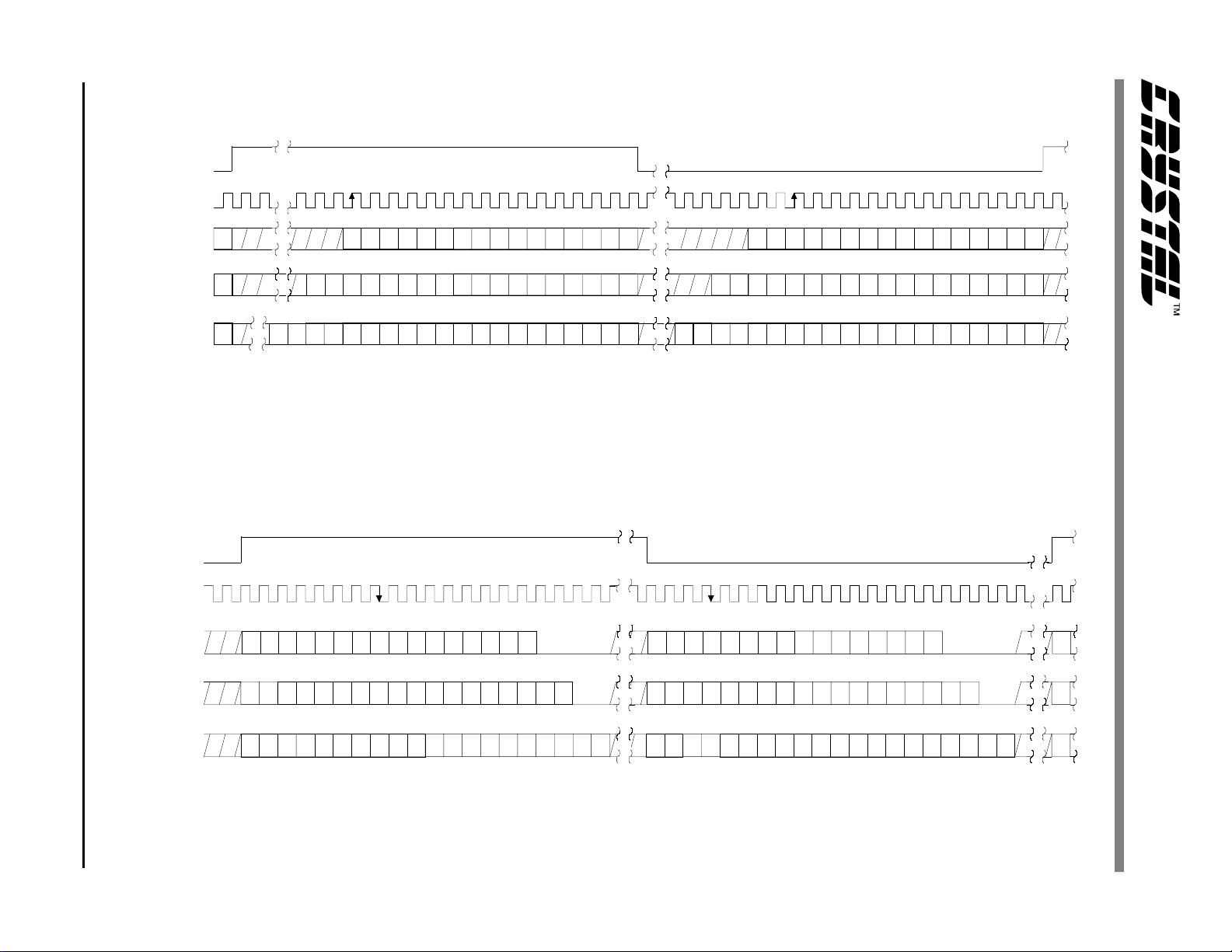
Formats 0, 1 and 2 are shown in Figure 3. The audio
data is right-justified, LSB aligned with the trailing
edge of LRCK, and latched into the serial input
data buffer on the rising edge of SCLK. Formats 0,
1 and 2 are 16, 18 and 20-b it versions and differ
only in the number of data bits required.
Formats 3 and 4 are 20-bit left justified, MSB
aligned with the leading edge of LRCK, and are
identical with the exception of the SCLK edge used
to latch data . Data is latc hed on t he fa lli ng edge of
SCLK in Format 3 a nd the rising edge of SCLK in
Format 4. Both form ats will suppo rt 16 an d 18-bit
inputs if the data is followed by four or two zeros to
simulate a 20-bit input as shown in Figures 4 and 5.
A very small of fset will result if th e 18 or 16-bit
data is follow ed by stat ic non-zero data.
2
Formats 5 and 6 are compatible with the I
S serial
data protocol and are shown in Figures 6 and 7. Notice that the MSB is delayed 1 period of SCLK following the leading edge of LRCK and LRCK is
inverted compared to the pre vious formats. Data is
latched on the rising edge of SCLK. Format 5 is 16-
2
S while Format 6 is 20-bit I2S. 18-bit I2S can
bit I
be implemented in Format 6 if the data is followed
by two zeros to simulate a 20-bit inpu t as shown in
Figure 7. A very small offset will result if the 18-bit
data is follow ed by stat ic non-zero data.
Serial Data Interface
The Seri al Data interfac e is accomplis hed via the
serial data input, SDATA, serial data clock, SCLK,
and the left/r ight clock, LRCK . The CS4329 supports seven seri al data formats wh ich are select ed
via the digital input format pins DIF0, DIF1 and
DIF2. The different formats control the relationship of LRCK to the serial data and the edge of
DIF2 DIF1 DIF0 Format Figure
00003
00113
01023
01134
10045
10156
11067
111Calibrate-
SCLK used t o latch t he data into th e input b uffer.
Table 2 lists the seven formats, along with the associated fi gu re numb er. The s er ial dat a is re pres en ted
8 DS153F1
Table 2. Digital Input Formats
DS153F1 9
LRCK
SCLK
SDATA
Format 0
SDATA
Format 1
SDATA
Format 2
LRCK
SCLK
Left Channel
0
0
0
19 18
15 14 13 12 11 10
15 14 13 12 11 10
17 16
15 14 13 12 11 1017 16
6543210987
6543210987
6
54321098 7
1819
15 14 13 12 11 10
17
15 14 13 12 11 10
16
17 16
15 14 131211 10
Right Channel
6543210987
6543210987
6543210987
NOTE: Format 1 is not compatible with CS4390
Figure 3. Digital Input Format 0, 1 and 2.
Left Channel
Right Channel
SDATA
16-Bit
SDATA
18-Bit
SDATA
20-Bit
15 14 15 14
16
15 14 13 12 11 10 654321098715 14 13 12 11 10
17
19 18
4321076513 12 11 10 9 8 654321098713 12 11 10
6
543210987
654321098715 14 13 12 11 1017 16
17 16
19 18
Figure 4. Digital Input Format 3.
15
17
654321098715 14 13 12 11 1017 16
19
CS4329
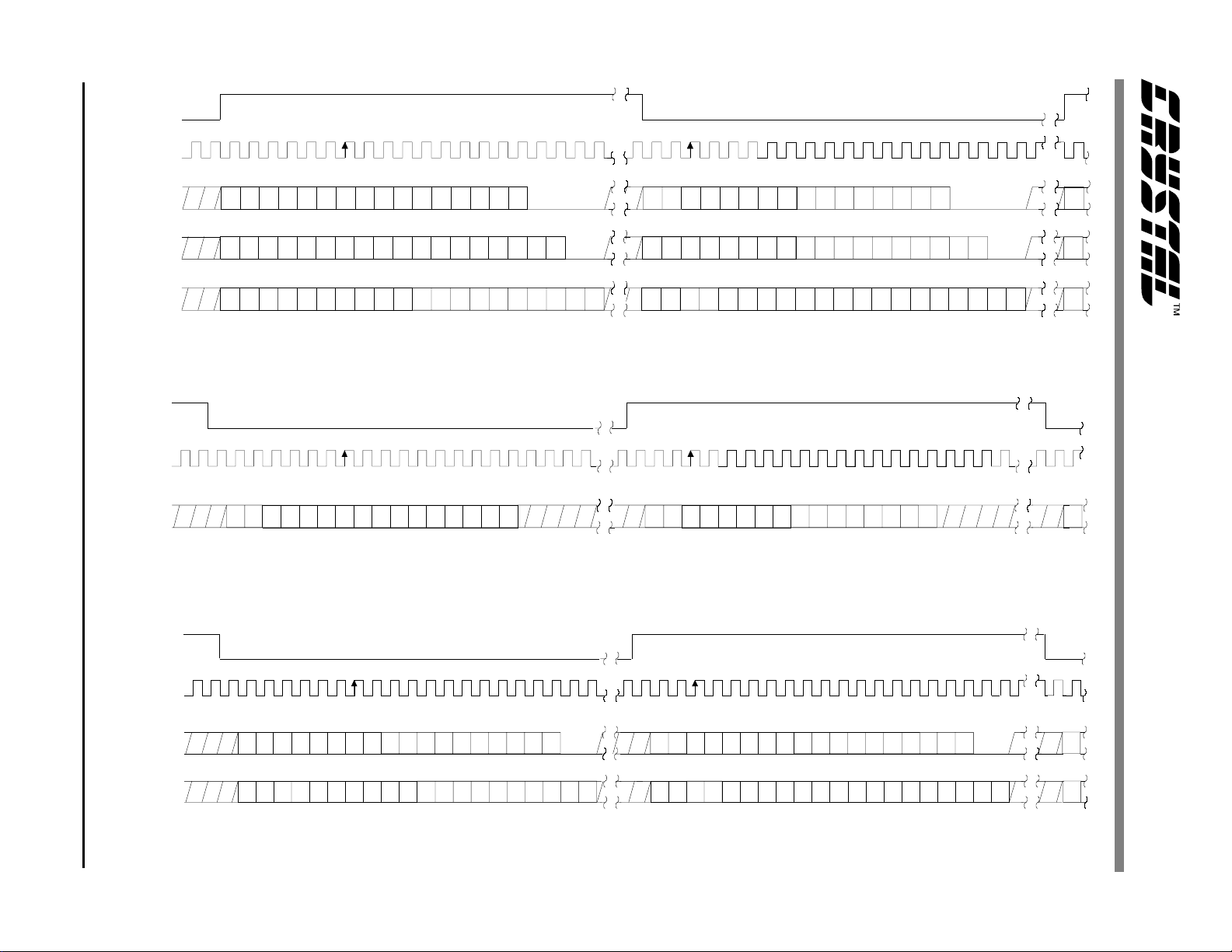
10 DS153F1
LRCK
SCLK
Left Channel
Right Channel
SDATA
16-Bit
SDATA
18-Bit
SDATA
20-Bit
LRCK
SCLK
SDATA
16-Bit
15 14 15 14
16
15 14 13 12 11 10 654321098715 14 13 12 11 10
17
14 13 12 11 10
17
16
15
19 18
4321076513 12 11 10 9 8 654321098713 12 11 10
6
543210987
6543210987
17 16
19 18
Figure 5. Digital Input Format 4.
Left Channel Right Ch an ne l
7
15 14 13 12 11 10
98
654321
0
Figure 6. Digital Input Format 5.
9
6543210
8715 141312 11 10
15
17
5
6
4321098715 14 13 12 11 1017 16
19
15
LRCK
SCLK
SDATA
18-Bit
SDATA
20-Bit
15 14 13 12 11 10
17 16
19 18
Left Channel Right Channel
6543210987
654321098715 14 13 12 11 1017 16
17 16
19 18
17
16
15
14 13 12 11 10
Figure 7. Digital Input Format 6.
654321098715 14 13 12 11 10
17
CS4329
6543210987
19
CS4329
Serial Clock
The serial clo ck controls the shi fting of data into
the input dat a buffers. The CS4329 su pports both
external and internal serial clock generation modes.
External Serial Clock
The CS4329 will enter the external serial clock
mode if 15 or more high\low transitions are detected on the SCLK pin during any phase of the LRCK
period. When this mode is enabled, internal serial
clock mode can not be accessed without ret urning
to the power down mode.
Internal Serial Clock
In the Internal Serial Cl ock Mode, the seria l clock
is internally derived and synchronous with MCLK.
The interna l SCLK / LRCK ratio is al ways 64 and
operation in this mode is identical to operation with
an external serial clock synchron ized with L RCK.
The SCLK pin must be connected to DGND for
proper operation.
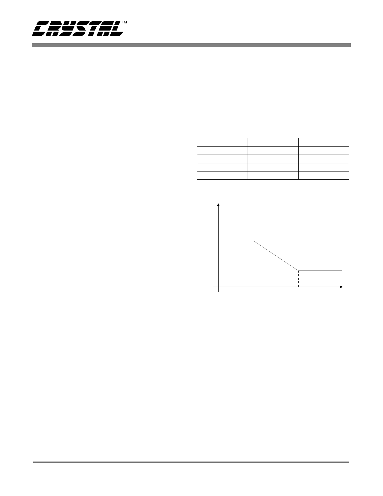
De-Emphasis
Implementation of digital de-emphasis requires reconfigu ration of th e digital f ilter to main tain the fi lter response sh own in Figure 8 at m ultipl e samp le
rates. The CS4 329 is capa ble of di gital de-e mphasis for 32, 44.1 or 48kHz sample rates. Table 3
shows the de-emphasis con trol inputs for DEM 0
and DEM 1.
DEM 1 DEM 0 De-emphasis
0032kHz
0144.1kHz
1048kHz
11OFF
Table 3. De-Emphasis Filter Selection
Gain
dB
µ
s
0dB
T1=50
The inte rnal serial clock mode is advant ageous in
that there are situations where improper serial
clock routin g on the printe d circuit board can degrade system pe rforma nce. The use of th e intern al
serial clock mode simplifies the routing of the
printed circ uit board by allowing the serial clock
trace to be deleted and avoids possible interference
effects.
Mute Functions
The CS4329 includes an auto-mute function which
will initiate a mute if 8192 consecutive 0’s or 1’s are
input on both the Left and Right channels. The
mute will be released when non-st at ic input data is
applied to the DAC. The auto-mute function is useful for applicat ions, such as com pact disk playe rs,
where the idle channel noise must be minimized.
This feature is active only if the AUTO_MUTE
is low and is independent of the status of MUTE_L
and MUTE_R. Either channel can also be muted
instantaneou sly with the MUTE_L or MUT E _R.
pin
F2
T2 = 15µs
Frequency
-10dB
F1
3.183 kHz
Figure 8. De-emphasis Filter Response
10.61 kHz
Initialization, Calibration and Power-Down
Upon initia l power -up, the DA C en te rs the po wer down mode. The interpolation filters and delta-sigma modulat ors are reset, and the in ternal voltage
reference, one-bit D/A converters and switched-capacitor low-pass filters are powered down. The device will remain in the power-down mode until
MCLK and LR CK are pres en te d. Once MCLK and
LRCK are detected, MCLK occurrences are counted over one LRCK period to determine the
MCLK/LRCK fre qu ency rati o. The ph ase and fre quency rela tionship between the two clocks m ust
remain fixed. If during any LRCK this relationship
DS153F1 11

CS4329
is changed, the CS4390 will reset. Power is applied
to the internal voltage ref erence, the D/A co nverters, switched-capacitor filters and the DAC will
then enter a calibration mode to properly set the
common m ode bia s volt age and minimi ze the differential offset. This initialization and calibration
sequence requires approximately 2700 cycles of
LRCK.
A offset cali bration c an also b e invok ed by taking
the Format select pins, DIF0, DIF1 and DIF2, to a
logic 1 as shown in Table 2. During calibration, the
differential outputs are shorted together and the
common-m ode voltage a ppears at the ou tput with
approxima tely an 8 kohm ou tput impedance . Following calibration, the analog output impedance
becomes less than 10 ohms and the common mode
voltage will move to approximat el y 2. 2 V .
The CS4329 will enter the power-down mode,
within 1 period of LRCK, if either MCLK or
LRCK is removed. The initialization sequence, as
described above , occurs when MCLK and LRCK
are restored.
Combined Digital and Analog Filter Response
The frequency response of the combined analog
switched-capacitor and digital filters is shown in
Figures 9, 10 and 11. The overall response is clock
dependent an d will sca le wit h Fs. Note t hat the response plots have been normalized to Fs and can be
de-normaliz ed by multiplyin g the X-axis scale b y
Fs, such as 48 kHz.
Analog Output and Filtering
The analog output should be operated in a differential mode which allows for the cancellation of common mode errors including noise, distortion and
offset voltage. E ac h output will prod uc e a nominal
2.83 Vpp (1 Vrms) output for a full scale digital input which equa te s to a 5. 66 Vpp (2Vrms) differen tial signal as shown in Figure 12.
0
-10
-20
-30
-40
-50
-60
Magnitude (dB)
-70
-80
-90
-100
0.0 0.1 0.2 0.3 0.4 0.5 0.6
Frequency (x Fs)
Figure 9. CS4329 Combin ed Digital a nd Analog Filter
Stopband Rejection
0
-10
-20
-30
-40
-50
-60
Magnitude (dB)
-70
-80
-90
-100
0.45 0.48 0.51 0.54
Frequency (x Fs)
Figure 10. CS4329 Combined Digital and Analog
Filter
0
-1
-2
-3
-4
-5
-6
Magnitude (dB)
-7
-8
-9
-10
0.46
Figure 11. Combined Digital and Analog Filter
0.47 0.48 0.49 0.50 0.51 0.52
Frequency (x Fs)
0.7
0.8 0.9 1.0
0.57
0.60
12 DS153F1

CS4329
Figure 13 displa ys the CS4329 outpu t noise spectrum. The n oise beyond the audio band c an be further reduced with additiona l analog filtering. The
applications note "Design Notes for a 2-Pole Fil te r
with Differential Input " discusses the second-order
Butterworth filter and differenti al to signal-ended
converter whi ch was impl emented on the CS4329
evaluation board, CDB4329. The CS4329 filter is a
linear phase design and does not include phase or
amplitude compensation for an external filter.
Therefore, the DAC system phase and amplitude
response will be de pendent on the external a nalog
circuitry .
CS4329
AOUT+
AOUT-
Full Scale Input level= (AIN+) - (AIN-)= 5.66 Vpp
Figure 12. Full Scale Input Voltage
0
-20
-40
-60
-80
-100
Magnitude (dB)
-120
-140
-160
0 .25 .50 .75 1.00 1.25
Frequency (x Fs)
Figure 13. CS4329 Output Noise Spectrum
1.50
1.75 2.00
(2.2 + 1.4)V
2.2V
(2.2 - 1.4)V
(2.2 + 1.4)V
2.2V
(2.2 - 1.4)V
2.25
2.50
Figure 1 shows the recom mended power arrange ments with VA connected to a clean +5volt supply.
VD should be derived from VA through a 10 Ω resistor. VD should not be used to powe r additional
digital circui try. All mode pins whi ch require VD
should be co nnected to pin 6 of the C S4329. All
mode pins which require DGND should be connected to pin 5 of the CS4329. Pins 4 and 5, AGND
and DGND, should be connected together at the
CS4329. DGND for the CS4329 should not be confused with the ground for the d igita l sec tion of the
system. The CS4329 should be positioned over the
analog ground plane near the digital/analog ground
plane spli t. The analog and digi tal ground planes
must be connected elsewhere in the system. The
CS4329 evaluation board, CDB4329, demonstrates
this layout technique. This technique minimizes
digital noise and insures proper power supply
matching and sequencing. Decoupling capacitors
should be lo cated as nea r to the CS432 9 as possible.
Performance Plots
The follow ing collect ion of CS4329 measure ment
plots were taken from the CDB4329 evaluation
board using the Audio Precision Dual Domain System Two.
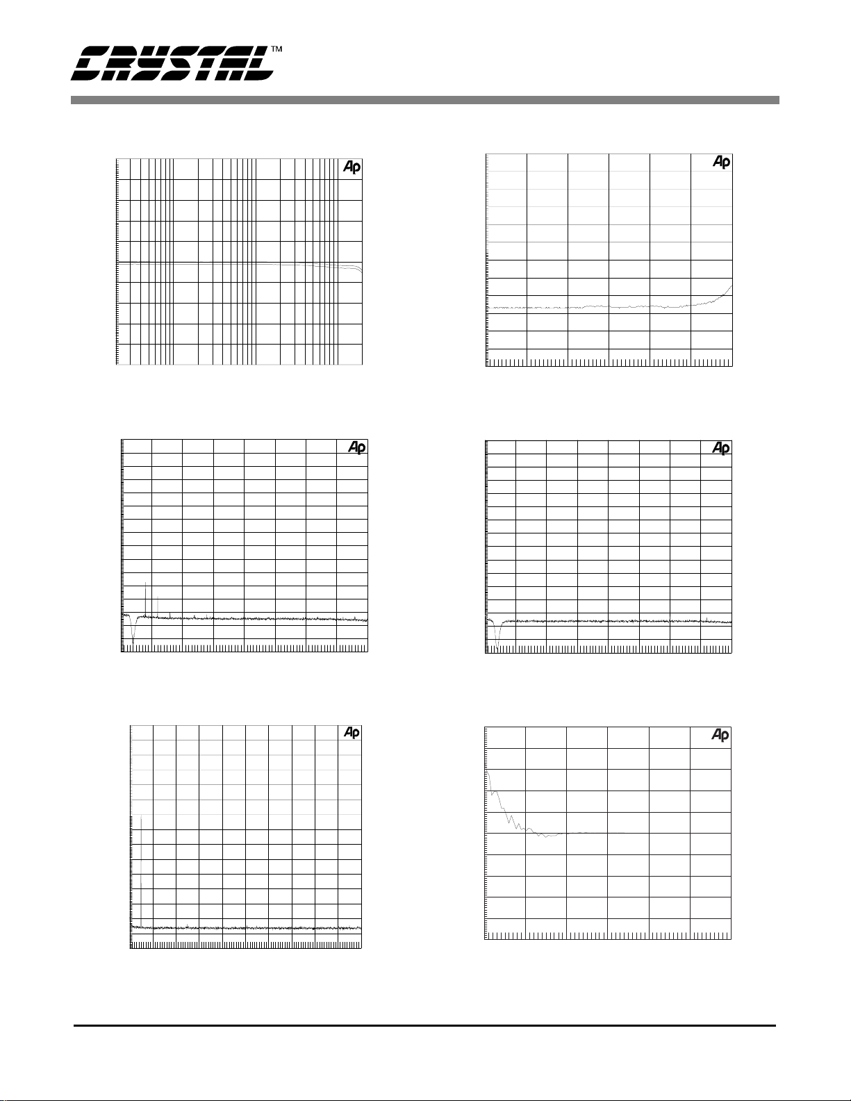
Figure 14 shows the frequency response at a
48 kHz sample ra te. The respo nse i s fl at to 20 kHz
+/-0.1 dB as spec i f ie d.
Figure 15 shows THD+ N versus signal amplit ude
for a 1 kHz 20-bit dithered input signal. Notice that
the there is no increase in disto rtion as the signal
level decreases. This indicates very good low-level
linearity, one of the key benefits of delta-sigma
digital to ana log convers ion.
Figure 16 shows a 16 k FFT of a 1 kHz ful l-scale
Grounding and Power Supply Decoupling
As with any high resolution converter, the CS4329
requires careful attention to power supply and
grounding ar rangement s to optim ize performa nce.
input signal. The signal has been filtered by a notch
filter within the System Two to remove the fundamental component of the signal. This minimizes
the distortion created in the analyzer analog-to-digital converter. This technique is discussed by Audio
DS153F1 13

CS4329
Precision i n the 10th an niversary ad dition of A UDIO.TST.
Figure 17 shows a 16 k FFT of a 1 kHz -20 dBFS
input signal. The signal has been filtered by a notch
filter within the Syste m T wo to re mov e the fun damental com ponent of the signal.
Figure 18 shows a 16 k FFT of a 1 kHz -60 dBFS
input signal.
Figure 19 shows the fade-to-noise linearity. The input signal is a dithered 20-bit 500 Hz sine wave
which fades from -60 to -120 dBFS. During the
fade, the o utp ut fro m t he CS4 329 is meas ured and
compared t o the ideal level. Notice the very close
tracking of the output level to the ideal, even at low
level inputs. The gradual shift of the plot away
from zero at signals l evels < - 110 dB i s caused b y
the background noise starting to dominate the measurement.
14 DS153F1
CS4329
+1
+0.8
+0.6
+0.4
+0.2
d
B
+0
r
A
-0.2
-0.4
-0.6
-0.8
-1
20 20k50 100 200 500 1k 2k 5k 10k
Hz
Figure 14. Frequency Response Figure 15. THD+N vs. Amplitude
+0
-10
-20
-30
-40
-50
-60
d
-70
B
r
-80
A
-90
-100
-110
-120
-130
-140
-150
-160
2.5k 20k5k 7.5k 10k 12.5k 15k 17.5k
Hz
Figure 16. 0 dBFS FFT Figure 17. -20 dBFS FFT
-60
-65
-70
-75
-80
-85
d
B
-90
r
A
-95
-100
-105
-110
-115
-120
-60 +0-50 -40 -30 -20 -10
dBFS
+0
-10
-20
-30
-40
-50
-60
-70
d
B
-80
r
-90
A
-100
-110
-120
-130
-140
-150
-160
2.5k 20k5k 7.5k 10k 12.5k 15k 17.5k
Hz
+0
-10
-20
-30
-40
-50
-60
d
-70
B
r
-80
A
-90
-100
-110
-120
-130
-140
-150
2k 20k4k 6k 8k 10k 12k 14k 16k 18k
Hz
+5
+4
+3
+2
+1
d
B
-0
r
A
-1
-2
-3
-4
-5
-120 +0-100 -80 -60 -40 -20
dBFS
Figure 18. -60 dBFS FFT Figure 19. Fade-to-Noise Linearity
DS153F1 15

PIN DESCRIPTIONS
CS4329
PDIP and SSOP
SDATA
Power Supply Connections
VA - Positive Analog Power, PIN 3.
Positive analog sup ply. Nominally +5 volts.
VD - Positive Digital Power, PIN 6.
Positive supply fo r the digital section. Nomina lly +5 volts.
AGND - Analog Ground, PIN 4.
DEM0
DEM1
VA
AGND
DGND
VD
LRCK
MCLK
SCLK
1
2
3
4
5
6
7
8
9
20
19
18
17
16
15
14
13
12
10 11
DIF0
DIF11
AOUTL+
AOUTLMUTE_ L
MUTE_ R
AO UT R+
AO UT RDIF2
AUTO-MUTE
Analog ground reference.
DGND - Digital Ground, PIN 5.
Digital ground for the digita l section.
Analog Outputs
AOUTR+,AOUTR- - Differential Right Channel Analog Outputs, PIN 14, PIN 13.
Analog output connections for the Right channel differential outputs. Nominally 2 Vrms
(differential ) for full-sca le digital in put signa l.
AOUTL+,A OUTL- - Differential Left Chan nel Analog O utputs , PIN 18, PI N 17.
Analog output connections for the Left channel differential outputs. Nominally 2 Vrms
(differential ) for full-sca le digital in put signa l.
16 DS153F1

Digital Inputs
MCLK - Clock Input, PIN 8.
The freque ncy must b e either 25 6×, 384× or 51 2× the i nput sample rate (Fs).
LRCK - Left/Right Clock, PIN 7.
This input determines which channel is currently being input on the Serial Data Input pin,
SDATA. The format of LRCK is controlled by D IF0, DIF1 and DIF2.
SCLK - Serial Bit Input Clock, PIN 9.
Clocks the individual bits of the serial data in from the SDATA pin. The edge used to latch
SDATA is controlled by DIF0, DIF1 and DIF2.
SDATA - Serial Data Input, PIN 10.
Two's complement MSB-first serial data of either 16, 18 or 20 bits is input on this pin. The
data is clocked into the CS4329 via the SCLK clock and the channel is determined by the
LRCK clock. T he format for the previous two clo cks is determin ed by the Digital Input Format
pins, DIF0, DIF1 and DIF2.
CS4329
DIF0, DIF1, DIF2 - Digital Input Format, PINS 20, 19, 12
These three p ins select one o f seven format s for the inco ming serial data stream. These pins set
the format of the SCLK and LRCK clocks with respect to SDATA. The formats are listed in
Ta b l e 2 .
DEM0, DEM1 - De-Emphasis Select, PINS 1, 2.
Controls th e activation of the standard 50/15us de-emp hasis filter for ei ther 32, 44.1 or 48 kHz
sample rates.
AUTO-MUTE
When Auto-Mute is low the analog outputs are muted following 8192 consecutive LRCK
cycles of stati c 0 or 1 data . Mute is cance led with th e return of non -static inp ut data.
MUTE_R
MUTE_L
muting funct ion for the Right channe l.
- Automatic Mute on Zero-Data, PIN 11.
, MUTE_L M ute, PINS 15, 16.
low activates a muting function for the Left channel. MUTE_R low activates a
DS153F1 17

PARAMETER DEFINITIONS
Dynamic Range
The ratio of the full scale rms value of the signal to the rms sum of all other spectral
components over the specified bandwidth. Dynamic range is a signal-to-noise measurement
over the specifi ed bandwidth made with a -60 dBFS signal. 60 dB is then added to the resulting
measurement to refer the measurement to full scale. This tech nique ensures that the distortio n
components are below the noise level and do not effect the measurement. This measurement
technique has been accepted by the Audio Engineering Society, AES17-1991, and the
Electronic Industries Asso ciation of Japan, EIAJ CP- 307.
Tot al Harmonic Di stortion + Nois e
The ratio of the rms value of the signal to the rms sum of all other spectral components over
the specified bandwidth (typically 10 Hz to 20 kHz), including distortion components.
Expressed in decibels.
Idle Channel Noise / Signa l-to-Noise-Ratio
The ratio of the rms analog output level with 1kHz full scale digital input to the rms analog
output level w ith all zeros into the digit al input. Measured A-w eighted over a 10 Hz to 20 kHz
bandwidth. Units in decibels. This specification has been standardized by the Audio
Engineering Society, AES17-1991, and re ferred to as Idle Channe l Noise. This sp ecific ation has
also been standardized by the Electronic Industries Association of Japan, EIAJ CP-307, and
referred to a s Signal-to-N oise-Ratio.
CS4329
Interchannel Isolation
A measure of crosstalk between the left and right channels. Measured for each channel at the
converter’s output with all zeros to the input under test and a full-scale signal applied to the
other channel . Units in deci bels.
Frequency R esponse
A measure of th e amplitude response v ariation from 10 Hz t o 20 kHz re lative to the ampl itude
response at 1 kHz. Uni ts in decibels.
De-Emphasis Error
A measure of the difference between the ideal de-emphasis filter and the actual de-emphasis
filter response. Me asured from 1 0 Hz to 20 kHz rel ative to 1 kHz. Units i n decibels.
Interchannel Gain Mismatch
The gain di fference be tween le ft and right channe ls. Units in decibe ls.
Gain Error
The devia tion from th e nomin al full sc ale analo g output f or a full sc ale dig ital input .
Gain Drift
The change in gain value with t empera ture. Un its in ppm /°C.
18 DS153F1

PACKAGE DIMENSIONS
N
CS4329
20L SSOP PACKAGE DRAWING
1
23
TOP VIEW
D
E
e
2
b
SIDE VIEW
A2
A1
A
SEATING
PLANE
L
1
E1
END VIEW
INCHES MILLIMETERS NOTE
DIM MIN MAX MIN MAX
A -- 0.084 -- 2.13
A1 0.002 0.010 0.05 0.25
A2 0.064 0.074 1.62 1.88
b 0.009 0.015 0.22 0.38 2,3
D 0.272 0.295 6.90 7.50 1
E 0.291 0.323 7.40 8.20
E1 0.197 0.220 5.00 5.60 1
e 0.022 0.030 0.55 0.75
L 0.025 0.041 0.63 1.03
∝ 0° 8° 0° 8°
Notes: 1. “D” and “E1” are reference datums and do not included mold flash or protrusions, but do include mold
mismatch and are measured at th e parting line, mold flash or pr otrusions shall not exce ed 0.20 mm per
side.
2. Dimension “b” does not include dambar protrusion/intrusion. Allowable dambar protrusion shall be
0.13 mm total in excess of “b” dimension at maximum material condition. Dambar intrusion shall not
reduce dimension “b” by more than 0.07 mm at least material conditi on.
3. These dimensions apply to the flat section of the lead between 0.10 and 0.25 mm from lead tips.
DS153F1 19

20 PIN PLASTIC (PDIP) PACKAGE DRAWING
CS4329
D
1
TOP VIEW
E1
SEATING
PLANE
b1
e
BOTTOM VIEW
A
A2
A1
b
L
INCHES MILLIMETERS
DIM MIN MAX MIN MAX
A 0.000 0.210 0.00 5.33
A1 0.015 0.025 0.38 0.64
A2 0.115 0.195 2.92 4.95
b 0.014 0.022 0.36 0.56
b1 0.045 0.070 1.14 1.78
c 0.008 0.014 0.20 0.36
D 0.980 1.060 24.89 26.92
E 0.300 0.325 7.62 8.26
E1 0.240 0.280 6.10 7.11
e 0.090 0.110 2.29 2.79
eA 0.280 0.320 7.11 8.13
eB 0.300 0.430 7.62 10.92
eC 0.000 0.060 0.00 1.52
L 0.115 0.150 2.92 3.81
∝
0° 15° 0° 15°
eB
E
∝
eA
SIDE VIEW
eC
c
20 DS153F1

CDB4329
CDB4390
Evaluation Board for CS4329 and CS4390
Features
l
Demonstrates recommended layout
and grounding arrangements
l
CS8412 Receives AES/EBU, S/PDIF,
& EIAJ-340 Compatible Digital Audio
l
Digital and Analog Patch Areas
l
Requires only a digital signal source
and power supplies for a complete Digital-toAnalog-Converter system
I
Description
The CDB4329/90 evaluation board is an excellent
means for quickly evaluating the CS4329 or CS4390 24bit, stereo D/A converter. Evaluation requires an analog
signal analyzer, a digital signal source and a power supply. Analog outputs are provided via RCA connectors for
both channels.
The CS8412 digital audio receiver I.C. provides the system timing necessary to operate the CS4329/90 and will
accept AES/EBU, S/PDIF, and EIAJ-340 compatible
audio data. The evaluation board may also be configured to accept external timing signals for operation in a
user application during system development.
ORDERING INFO
CDB4329
CDB4390
I/O for
Clocks
and Data
CS8412
Digital
Audio
Interface
Preliminary Product Information
Cirrus Logic, Inc.
Crystal Semiconductor Products Division
P.O. Box 17847, Austin, Texas 78760
(512) 445 7222 FAX: (512) 445 7581
http://www.crystal.com
CS4329
or
CS4390
This document contains information for a new product.
Cirrus Logic reserves the right to modify this product without notice.
Copyright Cirrus Logic, I nc. 1997
(All Rights Reserv ed)
Analog
Filter
DS153DB3
NOV ‘97
21

CDB4329 CDB4390
CDB4329/90 SYSTEM OVERVIEW
The CDB4329/90 evaluation board is an excellent
means of quickly evaluating the CS4329/90. The
CS8412 digital audio interface receiver provides an
easy interface to digital audio signal sources including the majority of digital audio test equipment. The evaluation board also allows the user to
supply clocks and data through a 10-pin header for
system development.
The CDB4329/90 schematic has been partitioned
into 8 schematics shown in Figures 2 through 9.
Each partitioned schematic is represented in the
system diagram shown in Figure 1. Notice that the
system diagram also includes the interconnections
between the partitioned schematics.
CS4329/90 Digital to Analog Converter
A description of the CS4329 or CS4390 is included
in the CS4329 and CS4390 data sheets.
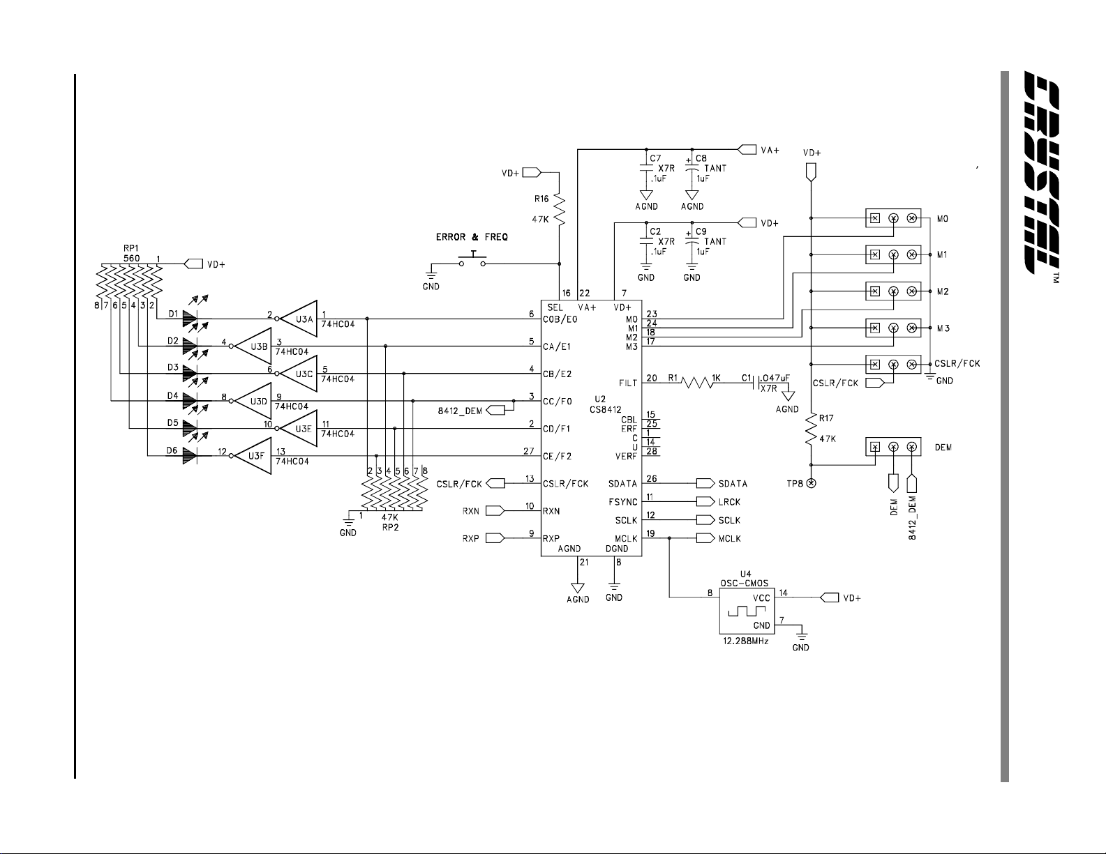
CS8412 Digital Audio Receiver
The system receives and decodes the standard
S/PDIF data format using a CS8412 Digital Audio
Receiver, Figure 9. The outputs of the CS8412 include a serial bit clock, serial data, left-right clock
(FSYNC), de-emphasis control and a 256Fs master
clock.
During normal operation, the CS8412 operates in
the Channel Status mode where the LED ’s display
channel status information for the channel selected
by the CSLR/FCK jumper. This allows the CS8412
to decode and supply the de-emphasis bit from the
digital audio interface for control of the CS4329/90
de-emphasis filter via pin3, CC/F0, of the CS8412.
When the Error Information Switch is activated,
the CS8412 operates in the Error and Frequency information mode. The information displayed by the
LED’s can be decoded by consulting the CS8412
data sheet. If the Error Information Switch is activated, the CC/F0 output has no relation to the deemphasis bit and it is likely that the de-emphasis
control for the CS4329/90 will be erroneous and
produce an incorrect audio output.
Encoded sample frequency information can be displayed provided a proper clock is being applied to
the FCK pin of the CS8412. When an LED is lit,
this indicates a "1" on the corresponding pin located on the CS8412. When an LED is off, this indicates a "0" on the corresponding pin. Neither the L
or R option of CSLR/FCK should be selected if the
FCK pin is being driven by a clock signal.
The evaluation board has been designed such that
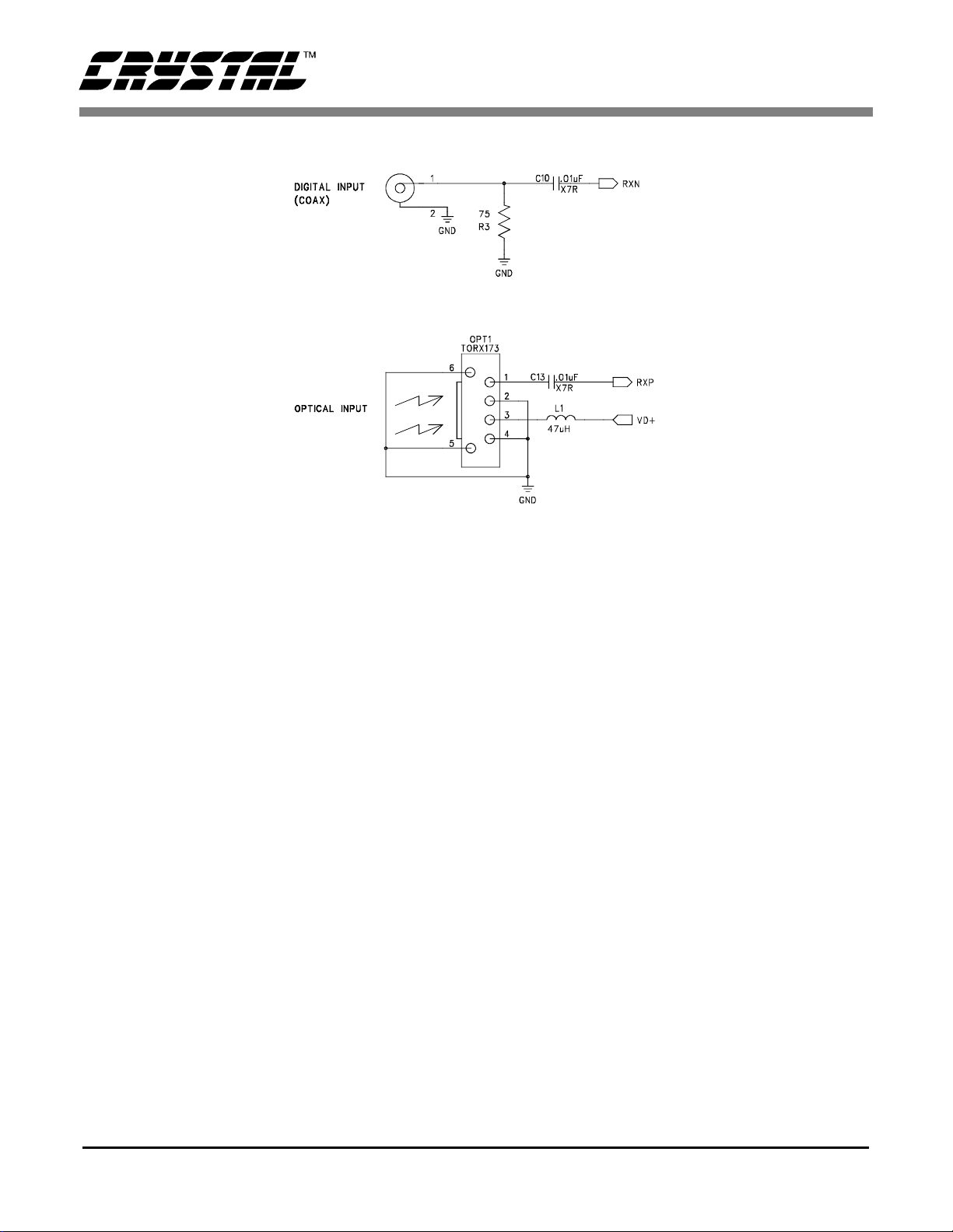
the input can be either optical or coax, Figure 8. It
is not necessary to select the active input. However,
both inputs can not be driven simult aneously.
Data Format
The CS4329/90 must be configured to be compatible with the incoming data and can be set with
DIF0, DIF1, and DIF2. The CS8412 data format
can be set with the M0, M1, M2 and M3. There are
several data formats which the CS8412 can produce that are compatible with CS4329/90. Refer to
Table 2 for one possibility.
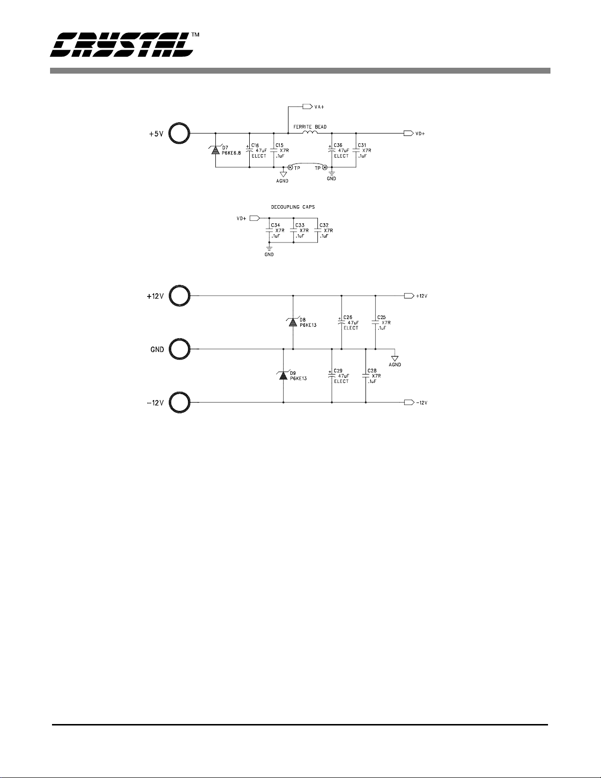
Power Supply Circuitry
Power is supplied to the evaluation board by four
binding posts, Figure 10. The +5 Volt input supplies power to the CS4329/90 (through VA+), the
CS8412 (through VA+ and VD+), a nd t he +5 Volt
digital circuitry (through VD+). The ±12 volt input
supplies power to the analog filter circuitry.
Input/Output for Clocks and Data
The evaluation board has been designed to allow
the interface to external systems via the 10-pin
header, J1. This header allows the evaluation board
to accept externally generated clocks and data. The
schematic for the clock/data I/O is shown in Figure
7. The 74HC243 transceiver functions as an I/O
buffer where the CLK SOURCE jumper determines if the transceiver operates as a transmitter or
receiver.
22 DS153DB3

CDB4329 CDB4390
The transceiver operates as a trans mitter with the
CLK SOURCE jumper in the 8412 position.
LRCK, SDATA, and SCLK from the CS8412 will
be available on J1. J22 must be in the 0 position and
J23 must be in the 1 position for MCLK to be an
output and to avoid bus contention on MCLK.
The transceiver operates as a receiver with the CLK
SOURCE jumper in the EXTERNAL position.
LRCK, SDATA and SCLK on J1 be come inputs.
The CS8412 must be removed from the evaluation
board for operation in this mode.
There are 2 options for the source of MCLK in the
EXT CLK source mode. MCLK can be an input
with J23 in the 1 position and J22 in the 0 position.
However, the recommended mode of operation is
to generate MCLK on the evaluation board. MCLK
becomes an output with LRCK, SCLK and SDATA inputs. This technique insures that the
CS4329/90 receives a jitter free clock to maximize
performance. This c an be accom plished by install ing a crystal oscillator into U4, see Figure 9 (the
socket for U4 is located within the footprint for the
CS8412) and placing J22 in t he 1 position a nd J23
in the 0 position.
Analog Filter
The design of the second-order Butterworth lowpass filter, Figure 6, is discussed in the CS4329 and
CS4390 data sheets and the applications note "Design Notes for a 2-pole Filter with Differential Input."
Grounding and Power Supply Decoupling
The CS4329/90 requires careful attention to power
supply and grounding arrangements to optimize
performance. The recommended power arrangements would be VA+ connected to a clean +5 Volt
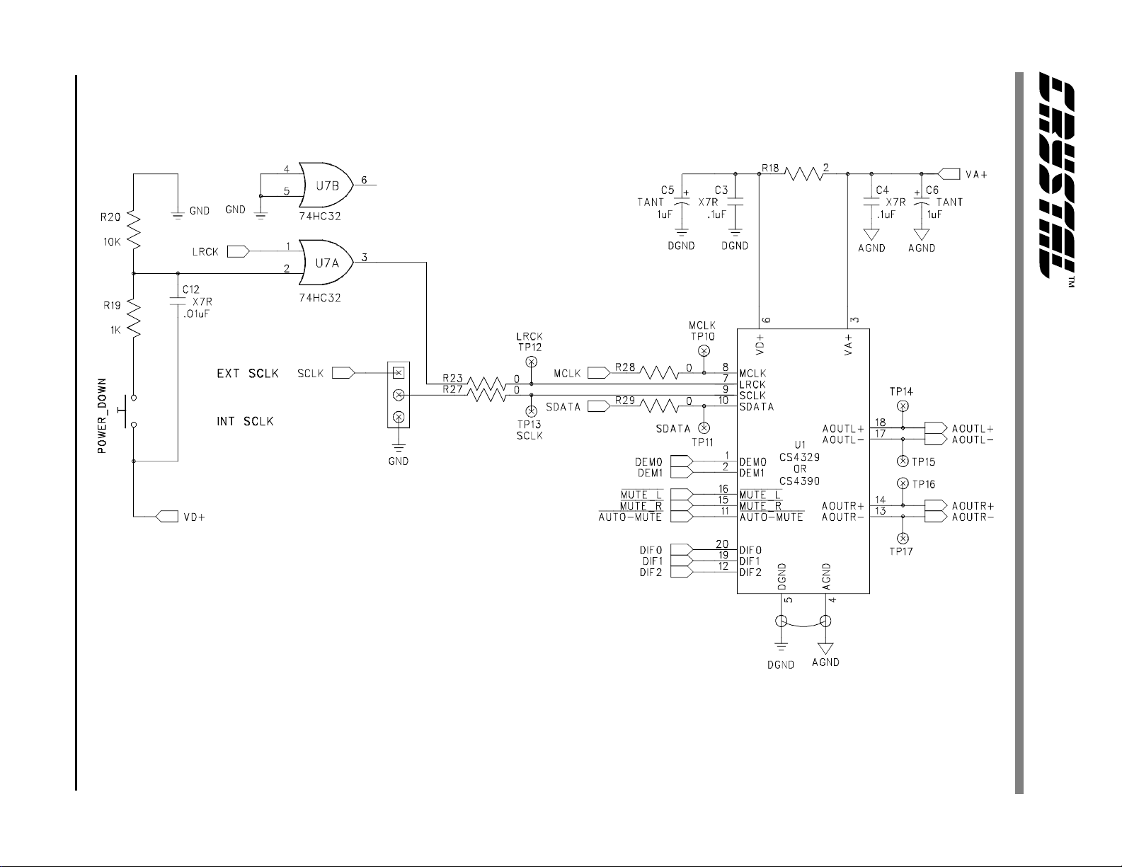
supply. The voltage VD+ (pin 6 of the CS4329/90)
should be derived from VA+ through a 2 ohm resistor and should not used for any additional digital
circuitry. Ideally, mode pins which require this
voltage should be connected directly to VD+ (pin 6
of the CS4329/90) and mode pins which require
DGND should be connected directly to pin 5 of the
CS4329/90. AGND and DGND, Pins 4 and 5, are
connected together at the CS4329/90. However, it
was not possible to connect VD+ (pin 6 of the
CS4329/90) and DGND to the mode pins on the
CDB4329/90 due to layout complications resulting
from the hardware selected to exercise the features
of the CS4329/90.
Figure 2 shows the CS4329/90 and connections.
The evaluation board has separate analog and digital regions with individual ground planes. DGND
for the CS4329/90 should not be confused with the
ground for the digital section of the system (GND).
The CS4329/90 is positioned over the analog
ground plane near the digital/analog ground plane
split. These ground planes are connected elsewhere
on the board. This layout technique is used to minimize digital noise and to insure proper power supply matching/sequencing. The decoupling
capacitors are located as close to the CS4329/90 as
possible. Extensive use of ground plane fill on both
the analog and digital sections of the evaluation
board yield large reductions in radiated noise effects.
DS153DB3 23

CDB4329 CDB4390
CONNECTOR INPUT/OUTPUT SIGNAL PRESENT
+5V input +5 Volts for the CS4329/90, CS8412 and digital section
±12V input ±12 volts for analog filter section
GND input ground connection from power supply
Digital input input digital audio interface input via coax
Optical input input digital audio interface input via optical
J1 input/output I/O for system clocks and digital audio data
AOUTL output left channel analog output
AOUTR output right channel analog output
Table 1. System Connections
JUMPER PURPOSE POSITION FUNCTION SELECTED
CSLR/FCK Selects channel for
CS8412 channel status
information
Clock Select Selects source of system
clocks and data
J22
J23
M0
M1
M2
M3
auto_mute CS4329/90 Auto Mute *Low
DEM0
DEM1
DIF0
DIF1
DIF2
SCLK CS4329/90 SCLK Mode *INT
DEM_8412 Selects source of de-
Selects MCLK as
input or output
CS8412 mode select *Low
De-emphasis select *High
CS4329/90 digital input
format
emphasis control
L
R
*8412
EXT
0
1
*Low
*Low
*Low
High
*Low
*High
*High
*Low
EXT
*Low
High
See CS8412 data sheet for details
CS8412 clock/data source
External clock/data source
See
Input/Output for Clocks and Data
text
See CS8412 data sheet for details
On
Off
See CS4329 and CS4390 data sheets for details
set for 44.1 kHz
See CS4329 and CS4390 data sheets for details
Internal SCLK Mode
External SCLK Mode
CS8412 de-emphasis
De-emphasis input static high
section of
Notes:1.* Default setting from factory
Table 2. CDB4329/90 Jumper Selectable Options
24 DS153DB3

CDB4329 CDB4390
Digital
Audio
Input
Fig 8 Fig 7
RXP
RXN
MCLK
LRCK
SCLK
CS8412
SDATA
I/O for
Clocks
and Data
Digital
Audio
Interface
CS4329
or
CS4390
AOUTL-
AOUTL+
AOUTR-
AOUTR+
Analog
Filter
Fig 6
Fig 9 Fig 2
MUTE_R
DEM0
DEM1
De-emphasis
Mode
MUTE_L
AUTOMUTE
Mute
Section
DIF0
DIF1
Calibration and
Format Select
Section
Fig 5Fig 4Fig 3
Figure 1. System Block Diagram and Signal Flow
DIF2
DS153DB3 25
26 DS153DB3
Figure 2. CS4329/90 and Connections
CDB4329 CDB4390
Figure 3. De-emphasis Circuitry
CDB4329 CDB4390
Figure 4. Mute Circuitry
Figure 5. Calibration and Format Select Circuitry
DS153DB3 27

NOTE: Rigth channel components in parentheses.
Figure 6. 2-pole Analog Filter
CDB4329 CDB4390
Figure 7. I/O Interface for Clocks and DATA
28 DS153DB3
CDB4329 CDB4390
OPTI Toshiba TORX173 optical receiver available from Insight Electronics
Figure 8. Digital Audio Input Circuit
DS153DB3 29
30 DS153DB3
Note: U2 and U4 can not be installed simultaneously .
Figure 9. CS8412 and Connections
CDB4329 CDB4390
CDB4329 CDB4390
Figure 10. Power Supply Connections
DS153DB3 31

CDB4329 CDB4390
Figure 11. CDB4329/90 Component Side Silkscreen
32 DS153DB3

CDB4329 CDB4390
Figure 12. CDB4329/90 Component Side (top)
DS153DB3 33

CDB4329 CDB4390
Figure 13. CDB4329/90 Solder Side (bottom)
34 DS153DB3

• Notes •

 Loading...