

CS42L51
Low Power, Stereo CODEC with Headphone Amp
DIGITAL to ANALOG FEATURES
! 98 dB Dynamic Range (A-wtd)
! -86 dB THD+N
! Headphone Amplifier - GND Centered
– On-Chip Charge Pump Provides -VA_HP
– No DC-Blocking Capacitor Required
– 46 mW Power Into Stereo 16 Ω @ 1.8 V
– 88 mW Power Into Stereo 16 Ω @ 2.5 V
– -75 dB THD+N
! Digital Signal Processing Engine
– Bass & Treble Tone Control, De-Emphasis
– PCM + ADC Mix w/Independent Vol Control
– Master Digital Volume Control
– Soft Ramp & Zero Cross Transitions
! Beep Generator
– Tone Selections Across Two Octaves
– Separate Volume Control
– Programmable On & Off Time Intervals
– Continuous, Periodic or One-Shot Beep
Selections
! Programmable Peak-Detect and Limiter
! Pop and Click Suppression
ANALOG to DIGITAL FEATURES
! 98 dB Dynamic Range (A-wtd)
! -88 dB THD+N
! Analog Gain Controls
– +32 dB or +16 dB MIC Pre-Amplifiers
– Analog Programmable Gain Amplifier
(PGA)
! +20 dB Digital Boost
! Programmable Automatic Level Control (ALC)
– Noise Gate for Noise Suppression
– Programmable Threshold and
Attack/Release Rates
! Independent Channel Control
! Digital Volume Control
! High-Pass Filter Disable for DC Measurements
! Stereo 3:1 Analog Input MUX
! Dual MIC Inputs
– Programmable, Low Noise MIC Bias Levels
– Differential MIC Mix for Common Mode
Noise Rejection
! Very Low 64 Fs Oversampling Clock Reduces
Power Consumption
Serial Audio
Input
Hardware
2
Mode or I
SPI Software
Mode
Control Data
Reset
Serial Audio
Output
1.8 V to 3.3 V
C &
Level Translator
1.8 V to 2.5 V 1.8 V to 2.5 V
Beep
Generator
PCM Serial Interface
Register
Configuration
Advance Product Information
http://www.cirrus.com
High Pass
Filters
1.8 V to 2.5 V
Digital
Signal
Processing
Engine
ALC
ALC
Volume
Controls
MUX
MUX
Multibit
∆Σ Modulator
Multibit
Oversampling
ADC
Multibit
Oversampling
ADC
Switched
Capacitor DAC
and Filter
Switched
Capacitor DAC
and Filter
MUX
PGA
MUX
PGA
Headphone
Amp - GND
Headphone
Amp - GND
MUX
Centered
Centered
Charge
Pump
+32 dB
+32 dB
MIC
Bias
Left HP Out
Right HP Out
Stereo Input 1
Stereo Input 2
Stereo Input 3 /
Mic Input 1 & 2
This document contains information for a new product.
Cirrus Logic reserves the right to modify this product without notice.
Copyright © Cirrus Logic, Inc. 2005
(All Rights Reserved)
SEPTEMBER '05
DS679A2

CS42L51
SYSTEM FEATURES
! 24-bit Converters
! 4 kHz to 96 kHz Sample Rate
! Multi-bit Delta Sigma Architecture
! Low Power Operation
– Stereo Playback: 12.93 mW @ 1.8 V
– Stereo Record and Playback: 20.18 mW @
1.8 V
! Variable Power Supplies
– 1.8 V to 2.5 V Digital & Analog
– 1.8 V to 3.3 V Interface Logic
! Power Down Management
– ADC, DAC, CODEC, MIC Pre-Amplifier,
PGA
! Software Mode (I²C & SPI™ Control)
! Hardware Mode (Stand-Alone Control)
! Digital Routing/Mixes:
– Analog Out = ADC + Digital In
– Digital Out = ADC + Digital In
– Internal Digital Loopback
– Mono Mixes
! Flexible Clocking Options
– Master or Slave Operation
– High-Impedance Digital Output Option (for
easy MUXing between CODEC and Other
Data Sources)
– Quarter-Speed Mode - (i.e. Allows 8 kHz Fs
while maintaining a flat noise floor up to
16 kHz)
APPLICATIONS
! HDD & Flash-Based Portable Audio Players
! MD Players/Recorders
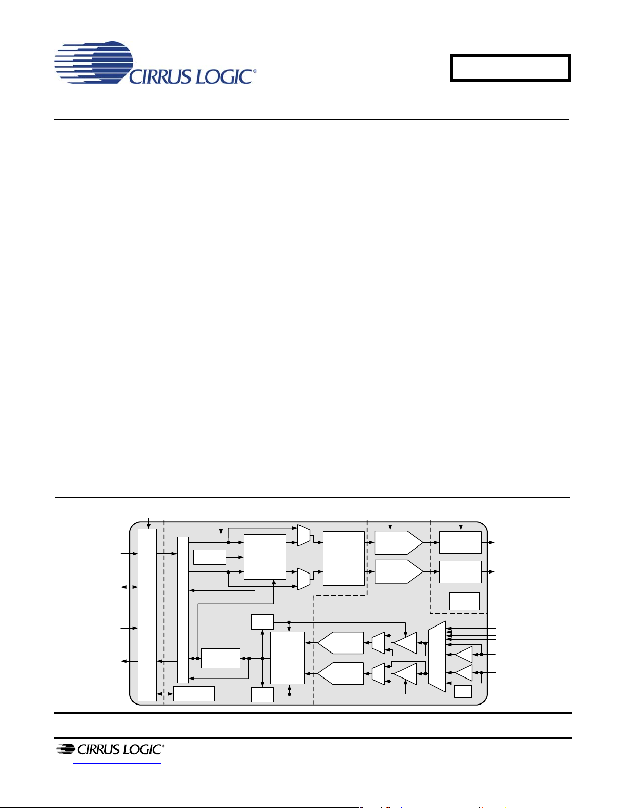
GENERAL DESCRIPTION
The CS42L51 is a highly integrated, 24-bit, 96 kHz, low
power stereo CODEC. Based on multi-bit, delta-sigma
modulation, it allows infinite sample rate adjustment between 4 kHz and 96 kHz. Both the ADC and DAC offer
many features suitable for low power, portable system
applications.
The ADC input path allows independent channel control
of a number of features. An input multiplexer selects between line-level or microphone level inputs for each
channel. The microphone input path includes a selectable programmable-gain pre-a mplifier stage and a low
noise MIC bias voltage supply. A PGA is available for
line or microphone inputs and provides analog gain with
soft ramp and zero cross transitions. The ADC also features a digital volume attenuator with soft ramp
transitions. A programmable ALC and Noise Gate monitor the input signals and adjust the volume levels
appropriately.
The DAC output path includes a digital signal pro cessing engine. Tone Control provides bass and treble
adjustment of four selectable corner frequencies. The
Mixer allows independent volume control for both the
ADC mix and the PCM mix, as well as a master digital
volume control for the analog output. All volume level
changes may be configured to occur on soft ramp and
zero cross transitions. The DAC also includes de-emphasis, limiting functions and a beep generator
delivering tones selectable across a range of two full
octaves.
The stereo headphone amplifier is powered from a separate positive supply and the integrated charge pump
provides a negative supply. This allows a gr ound-centered analog output with a wide signal swing and
eliminates external DC-blocking capacitors.
In addition to its many features, the CS42L51 operates
from a low-voltage analog and digital core, making this
CODEC ideal for portable systems that require extremely low power consumption in a minimal amount of
space.
! PDAs
! Personal Media Players
! Portable Game Consoles
! Digital Voice Recorders
! Digital Camcorders
! Digital Cameras
! Smart Phones
2 DS679A2
The CS42L51 is available in a 32-pin QFN package in
both Commercial (-10 to +70° C) and Automotive
grades (-40 to +85° C). The CDB42L51 Customer Demonstration board is also available for device evaluation
and implementation suggestions. Please see “Ordering
Information” on page 81 for complete details.

TABLE OF CONTENTS
1. PIN DESCRIPTIONS - SOFTWARE (HARDWARE) MODE .................................................... 7
1.1 Digital I/O Pin Characteristics ....................... ... ... .... ... ... .....................................................9
2. TYPICAL CONNECTION DIAGRAMS ................................................................................... 10
3. CHARACTERISTIC AND SPECIFICATION TABLES ........................................................... 12
SPECIFIED OPERATING CONDITIONS............................................................................... 12
ABSOLUTE MAXIMUM RATINGS.........................................................................................12
ANALOG INPUT CHARACTERISTICS (COMMERCIAL - CNZ)............................................ 13
ANALOG INPUT CHARACTERISTICS (AUTOMOTIVE - DNZ) ............................................ 14
ADC DIGITAL FILTER CHARACTERISTICS......................................................................... 15
ANALOG OUTPUT CHARACTERISTICS (COMMERCIAL - CNZ)........................................ 16
ANALOG OUTPUT CHARACTERISTICS (AUTOMOTIVE - DNZ) ........................................ 17
LINE OUTPUT VOLTAGE CHARACTERISTICS................................................................... 18
HEADPHONE OUTPUT POWER CHARACTERISTICS........................................................ 19
COMBINED DAC INTERPOLATION & ON-CHIP ANALOG FILTER RESPONSE................ 20
SWITCHING SPECIFICATIONS - SERIAL PORT.................................................................20
SWITCHING SPECIFICATIONS - I²C CONTROL PORT.......................................................22
SWITCHING CHARACTERISTICS - SPI CONTROL PORT..................................................23
DC ELECTRICAL CHARACTERISTICS .......... ... ... ... .... ...................................................... ... 24
DIGITAL INTERFACE SPECIFICATIONS & CHARACTERISTICS....................................... 24
POWER CONSUMPTION......................................................................................................25
4. APPLICATIONS ..................................................................................................................... 26
4.1 Overview ... ... .... ... ... ... .... ................................................................................................... 26
4.1.1 Architecture ......................................... ... .... ... ... ................................................... 26
4.1.2 Line & MIC Inputs ..................... .... ... ....................................................... ... ... ......26
4.1.3 Line & Headphone Outputs ........................ ... ... ... .... ... ... ... ... ................................ 26
4.1.4 Signal Processing Engine ................... ... .... ... ... ... .... ... ......................................... 26
4.1.5 Beep Generator ..................... ... .... ... ... ... .... ... ... ... ................................................ 26
4.1.6 Device Control (Hardware or Software Mode) .................................................... 26
4.1.7 Power Management ............................................ .... ... ... ... ... .... ............................ 26
4.2 Hardware Mode .. ....................................................... ... ... .... ... ... ...................................... 27
4.3 Analog Inputs ............................................................... ... .... ............................................ 28
4.3.1 Digital Code, Offset & DC Measurement ............................................................ 28
4.3.2 High-Pass Filter and DC Offset Calibration ........................................................ 29
4.3.3 Digital Routing ..................... ... ....................................................... ... ................... 29
4.3.4 Differential Inputs ................ ... ....................................................... ... .... ... ... ... ......29
4.3.4.1 External Passive Components ............. ............. ............. ................ ......... 29
4.3.5 Analog Input Multiplexer ..................................................................................... 30
4.3.6 MIC & PGA Gain .............................................. ... .... ............................................ 31
4.3.7 Automatic Level Control (ALC) ........................................................................... 31
4.3.8 Noise Gate .......... ... ... .... ... ... ... ... .......................................................................... 32
4.4 Analog Outputs .......................... ... ... ... ....................................................... ... .... ............... 33
4.4.1 De-Emphasis Filter ................ ... .... ... ... ... ....................................................... ... ... 33
4.4.2 Volume Controls ................. ... ... ....................................................... .... ... ............ 34
4.4.3 Mono Channel Mixer ...........................................................................................34
4.4.4 Beep Generator ..................... ... .... ... ... ... .... ... ... ... ................................................ 34
4.4.5 Tone Control ................................................. ... ... .... ... ... ...................................... 35
4.4.6 Limiter ................................................. ... .... .........................................................35
4.4.7 Line-Level Outputs and Filtering .........................................................................36
4.4.8 On-Chip Charge Pump ................. ... ... ... ....................................................... ... ... 36
4.5 Serial Port Clocking ............................................................. ... ... ... ... ................................ 37
4.5.1 Slave ......... ... .... ... ... ... .................................................... ... ... .... ... ... ...................... 37
4.5.2 Master ................................................................................................................. 38
CS42L51
DS679A2 3

CS42L51
4.5.3 High-Impedance Digital Output ........................................................................... 38
4.5.4 Quarter- and Half-Speed Mode ..................................... ... ... .... ... ... ... .... ... ... ... ... ... 39
4.6 Digital Interface Formats ................................................................................................. 39
4.7 Initialization ...................................................................................................................... 40
4.8 Recommended Power-Up Sequence .............................................................................. 40
4.9 Recommended Power-Down Sequence ......................................................................... 41
4.10 Software Mode ........... ... ... ... .... ... ... ... ....................................................... ... .... ... ... ... ... ... 42
4.10.1 SPI Control ........................... ... .... ... ... ... .... ... ... ... .... ... ......................................... 42
4.10.2 I²C Control ............................ ... .... ... ... ... .... ... ... ................................................... 42
4.10.3 Memory Address Pointer (MAP) ....................................................................... 44
4.10.3.1 Map Increment (INCR) ..........................................................................44
5. REGISTER QUICK REFERENCE ............. .......................................................... .... ... ... ... ... ... 45
6. REGISTER DESCRIPTION ................................................. ... .... ... ... ... ... ................................ 47
6.1 Chip I.D. and Revision Register (Address 01h) (Read Only) ............... ... ... ... .... ... ............ 47
6.2 Power Control 1 (Address 02h) ................................................. ... ... .... ... ... ... .... ... ... ... ... ... 47
6.3 MIC Power Control & Speed Control (Address 03h) ...................................................... 48
6.4 Interface Control (Address 04h) ...................................................................................... 49
6.5 MIC Control (Address 05h) .............................................................................................. 51
6.6 ADC Control (Address 06h) ............................................................................................. 52
6.7 ADCx Input Select, Invert & Mute (Address 07h) ............................................................ 53
6.8 DAC Output Control (Address 08h) ................................................................................. 54
6.9 DAC Control (Address 09h) ............................................................................................. 55
6.10 ALCX & PGAX Control:
ALCA, PGAA (Address 0Ah) & ALCB, PGAB (Address 0Bh) ..................................... 56
6.11 ADCx Attenuator:
ADCA (Address 0Ch) & ADCB (Address 0Dh) ............................................................ 57
6.12 ADCx Mixer Volume Control:
ADCA (Address 0Eh) & ADCB (Address 0Fh) ....................... ...................................... 58
6.13 PCMX Mixer Volume Control:
PCMA (Address 10h) & PCMB (Address 11h) .................... ................ ................ ......... 59
6.14 Beep Frequency & Timing Configuration (Address 12h) ............................................... 60
6.15 Beep Off Time & Volume (Address 13h) ....................................................................... 61
6.16 Beep Configuration & Tone Configuration (Address 14h) ............................................. 62
6.17 Tone Control (Address 15h) .............................................. ... ... ... ... .... ... ... ... .... ... ... ... ... ... 63
6.18 AOUTx Volume Control:
AOUTA (Address 16h) & AOUTB (Address 17h) ......................................................... 64
6.20 Limiter Threshold SZC Disable (Address 19h) .............................................................. 65
6.21 Limiter Release Rate Register (Address 1Ah) ...................................... ......................... 66
6.22 Limiter Attack Rate Register (Address 1Bh) ......................................... ......................... 67
6.23 ALC Enable & Attack Rate (Address 1Ch) .................................................................... 67
6.24 ALC Release Rate (Address 1Dh) ................................................................................. 68
6.25 ALC Threshold (Address 1Eh) ....................................................................................... 69
6.26 Noise Gate Configuration & Misc. (Address 1Fh) .................... ................................ ...... 70
6.27 Status (Address 20h) (Read Only) ............. ... ... .... ... ... ... .... ... ... ... ... .... ... ... ... .... ... ... ... ... ... 71
6.28 Charge Pump Frequency (Address 21h) ....................................................................... 71
7. ANALOG PERFORMANCE PLOTS ...................................................................................... 72
7.1 Headphone THD+N versus Output Power Plots ............................................................. 72
7.2 ADC_FILT+ Capacitor Effects on THD+N ....................................................................... 74
8. EXAMPLE SYSTEM CLOCK FREQUENCIES ...................................................................... 75
8.1 Auto Detect Enabled ........................................................................................................75
8.2 Auto Detect Disabled .......................................................................................................76
9. PCB LAYOUT CONSIDERATIONS .............................................. ... ... ... .... ... ... ... .... ... ... ... ... ... 77
9.1 Power Supply, Grounding ................................................................................................ 77
9.2 QFN Thermal Pad ........................................................................................................... 77
4 DS679A2

CS42L51
10. ADC & DAC DIGITAL FILTERS .......................................................................................... 78
11. PARAMETER DEFINITIONS ................................................................................................ 79
12. PACKAGE DIMENSIONS ................................................................................................... 80
THERMAL CHARACTERISTICS............................................................................................ 80
13. ORDERING INFORMATION ............................................................................................... 81
14. REFERENCES ................................................................................ ... ... .... ... ... ...................... 81
15. REVISION HISTORY ........................................................................................................... 82
DS679A2 5

LIST OF FIGURES
Figure 1. Typical Connection Diagram (Software Mode).......................................................................... 10
Figure 2. Typical Connection Diagram (Hardware Mode)......................................................................... 11
Figure 3. Headphone Output Test Load.................................................................................................... 19
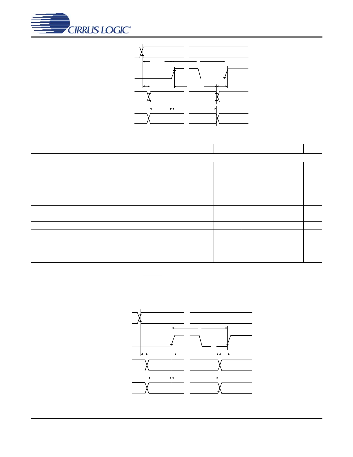
Figure 4. Serial Audio Interface Slave Mode Timing.................................................. .... ... ... ... ... .... ... ... ..... 21
Figure 5. TDM Serial Audio Interface Timing............................................................................................ 21
Figure 6. Serial Audio Interface Master Mode Timing............................................................................... 21
Figure 7. Control Port Timing - I²C............................................................................................................ 22
Figure 8. Control Port Timing - SPI Format............................................................................................... 23
Figure 9. Analog Input Architecture............................ ... ... .... ... ... ... ............................................................ 28
Figure 10. MIC Input Mix w/Common Mode Rejection.............................................................................. 30
Figure 11. Differential Input....................................................................................................................... 30
Figure 12. ALC................. ... ... .... ... ... ... ....................................................... ... .... ........................................ 31
Figure 13. Noise Gate Attenuation............................................. ... .... ........................................................ 32
Figure 14. Output Architecture.................................................................................................................. 33
Figure 15. De-Emphasis Curve................................................................................................................. 33
Figure 16. Beep Configuration Options............................................. ... ... ... ... .... ... ... ... .... ... ... ... ... .... ........... 34
Figure 17. Peak Detect & Limiter .............................................................................................................. 35
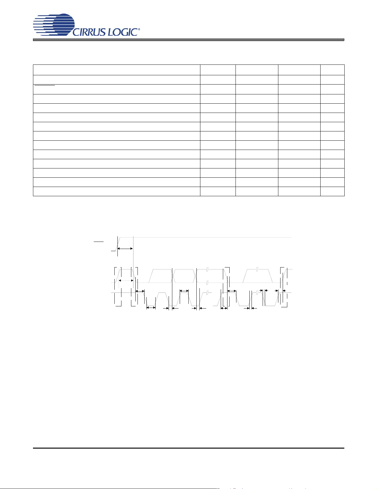
Figure 18. Master Mode Timing................................................................................................................ 38
Figure 19. Tri-State Serial Port ................................................................................................................. 38
Figure 20. I²S Format.................... ... ... .... ... ... ... ... .... ....................................................... ... ........................ 39
Figure 21. Left-Justified Format................................................................................................................ 39
Figure 22. Right-Justified Format (DAC only) ........................................................................................... 39
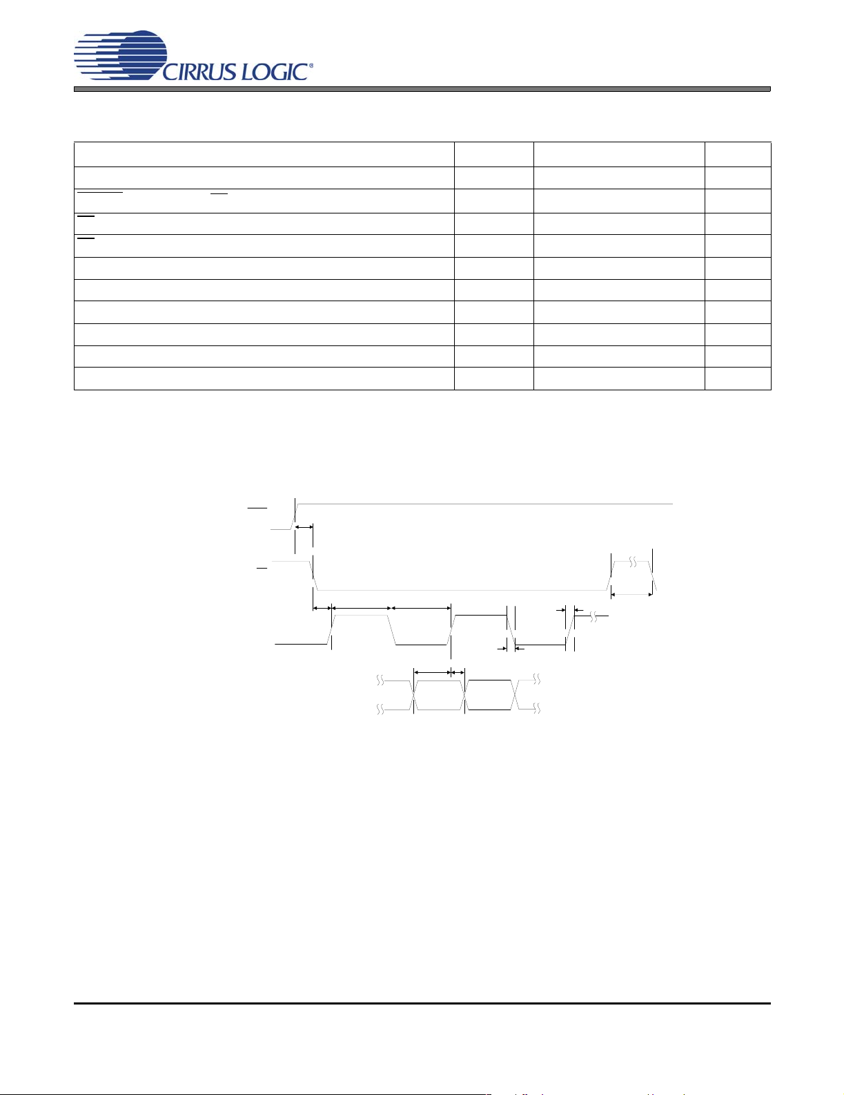
Figure 23. Initialization Flow Chart............................................................................................................ 41
Figure 24. Control Port Timing in SPI Mode ........................ ... ... ... .... ... ... ... ... .... ........................................ 42
Figure 25. Control Port Timing, I²C Write................................................... ... .... ... ... ... .... ... ... ... ... ............... 43
Figure 26. Control Port Timing, I²C Read............................. ... ... ... .... ... ... ... ... .... ... ... .................................. 43
Figure 27. AIN & PGA Selection ............................................................................................................... 53
Figure 28. THD+N vs. Ouput Power per Channel at 1.8 V (16 Ω load) .................................................... 72
Figure 29. THD+N vs. Ouput Power per Channel at 2.5 V (16 Ω load) .................................................... 72
Figure 30. THD+N vs. Ouput Power per Channel at 1.8 V (32 Ω load) .................................................... 73
Figure 31. THD+N vs. Ouput Power per Channel at 2.5 V (32 Ω load) .................................................... 73
Figure 32. ADC THD+N vs. Frequency w/Capacitor Effects..................................................................... 74
Figure 33. ADC Passband Ripple ............................................................................................................. 78
Figure 34. ADC Stopband Rejection......................................................................................................... 78
Figure 35. DAC Passband Ripple ............................................................................................................. 78
Figure 36. DAC Stopband......................................................................................................................... 78
Figure 35. DAC Transition Band ............................................................................................................... 78
Figure 36. DAC Transition Band (Detail)................................................................................................... 78
Figure 35. ADC Transition Band ............................................................................................................... 78
Figure 36. ADC Transition Band (Detail)................................................................................................... 78
CS42L51
6 DS679A2
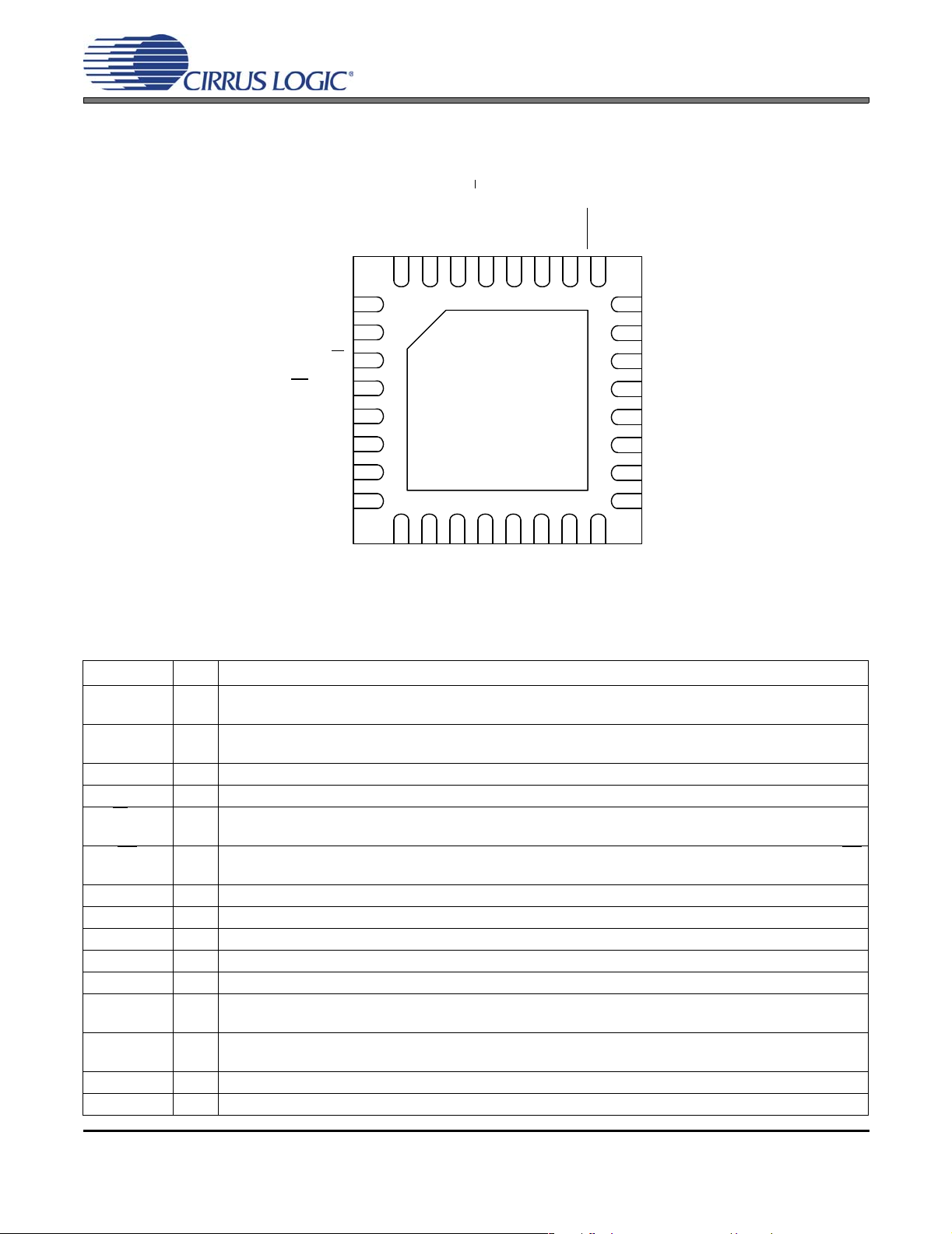
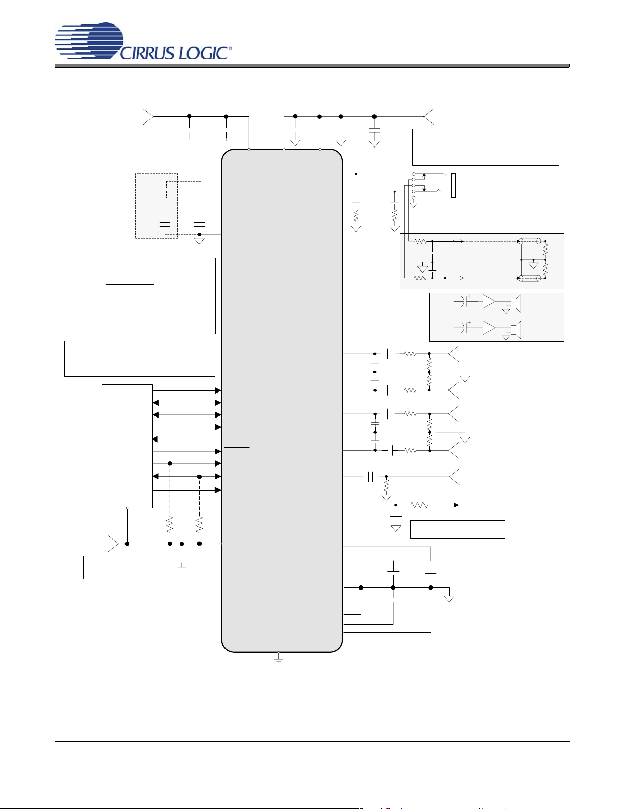
1. PIN DESCRIPTIONS - SOFTWARE (HARDWARE) MODE
)
CS42L51
RESET
VL
262728
25
AIN1B
24
AIN1A
23
AFILTB
22
AFILTA
21
20
AIN2B/BIAS
AIN2A
19
MICIN2/BIAS/AIN3B
18
MICIN1/AIN3A
17
VQ
ADC_FILT+
LRCK
SDA/CDIN (MCLKDIV2)
SCL/CCLK (I²S/LJ
AD0/CS
(DEM)
VA_HP
FLYP
GNDHP
FLYN
SDIN
SCLK
MCLK
SDOUT (M/S
303132
29
1
2
)
3
4
5
6
7
8
CS42L51
109
11
AOUTA
AOUTB
VSS_HP
12
VA
VD
DGND
13 14 15 16
AGND
DAC_FILT+
Pin Name # Pin Description
LRCK 1 Left Right Clock (Input/Output) - Determines which channel, Left or Right, is currently active on the
serial audio data line.
SDA/CDIN 2 Serial Control Data (Input/Output) - SDA is a data I/O in I²C mode. CDIN is the input data line for the
control port interface in SPI mode.
(MCLKDIV2) MCLK Divide by 2 (Input) - Hardware Mode: Divides the MCLK by 2 prior to all internal circuitry.
SCL/CCLK 3 Serial Control Port Clock (Input) - Serial clock for the serial control port.
(I²S/LJ
) Interface Format Selection (Input) - Hardware Mode: Selects between I²S & Left-Justified interface for-
mats for the ADC & DAC.
AD0/CS
(DEM) De-Emphasis (Input) - Hardware Mode: Enables/disables the de-emphasis filter.
VA_HP 5 Analog Power For Headphone (Input) - Positive power for the internal analog headphone section.
FLYP 6 Charge Pump Cap Positive Node (Input) - Positive node for the external charge pump capacitor.
GNDHP 7 Analog Ground (Input) - Ground reference for the internal headphone/charge pump section.
FLYN 8 Charge Pump Cap Negative Node (Input) - Negative node for the external charge pump capacitor.
VSS_HP 9 Negative Voltage From Charge Pump (Output) - Negative voltage rail for the internal analog head-
AOUTB
AOUTA
VA 12 Analog Power (Input) - Positive power for the internal analog section.
AGND 13 Analog Ground (Input) - Ground reference for the internal analog section.
4 Address Bit 0 (I²C) / Control Port Chip Select (SPI) (Input) - AD0 is a chip address pin in I²C mode; CS
is the chip select signal for SPI format.
phone section.
1011Analog Audio Output (Output) - The full-scale output level is specified in the DAC Analog Characteris-
tics specification table.
DS679A2 7
CS42L51
DAC_FILT+
ADC_FILT+1416
VQ 15 Quiescent Voltage (Output) - Filter connection for internal quiescent voltage.
MICIN1/
AIN3A
MICIN2/
BIAS/AIN3B
AIN2A 19 Analog Input (Input) - The full-scale level is specified in the ADC Analog Characteristics specification
AIN2B/BIAS 20 Analog Input (Input/Output) - The full-scale level is specified in the ADC Analog Characteristics specifi-
AFILTA
AFILTB
AIN1A
AIN1B
RESET
VL 26 Digital Interface Power (Input) - Determines the required signal level for the serial audio interface and
VD 27 Digital Power (Input) - Positive power for the internal digital section.
DGND 28 Digital Ground (Input) - Ground reference for the internal digital section.
SDOUT 29 Serial Audio Data Output (Output) - Output for two’s complement serial audio data.
(M/S
) Serial Port Master/Slave (Input/Output) - Hardware Mode Startup Option: Selects between master and
MCLK 30 Master Clock (Input) -Clock source for the delta-sigma modulators.
SCLK 31 Serial Clock (Input/Output) - Serial clock for the serial audio interface.
SDIN 32 Serial Audio Data Input (Input) - Input for two’s complement serial audio data.
Thermal Pad - Thermal relief pad for optimized heat dissipation. See “QFN Thermal Pad” on page 77.
Positive Voltage Reference (Output) - Positive reference voltage for the internal sampling circuits.
17 Microp hone Input 1 (Input) - The full-scale level is specified in the ADC Analog Characteristics specifi-
cation table.
18 Microp hone Input 2 (Input/Output) - The full-scale level is specified in the ADC Analog Characteristics
specification table. This pin can also be configured as an output to provide a low noise bias supply for an
external microphone. Electrical characteristics are specified in the DC Electrical Characteristics table.
table.
cation table. This pin can also be configured as an output to provide a low noise bias supply for an exter-
nal microphone. Electrical characteristics are specified in the DC Electrical Characteristics table.
2122Filter Connection (Output) - Filter connection for the ADC inputs.
2324Analog Input (Input) - The full-scale level is specified in the ADC Analog Characteristics specification
table.
25 Reset (Input) - The device enters a low power mode when this pin is driven low.
host control port. Refer to the Recommended Operating Conditions for appropriate voltages.
slave mode for the serial port.
8 DS679A2
CS42L51
1.1 Digital I/O Pin Characteristics
The logic level for each input should adhere to the corr esponding power rail and should not exceed the maximum
ratings.
Power
Rail
VL
Pin Name
SW/(HW)
RESET Input
SCL/CCLK
(I²S/LJ)
SDA/CDIN
(MCLKDIV2)
AD0/CS
(DEM)
MCLK Input
LRCK Input/Output
SCLK Input/Output
SDOUT
(M/S)
SDIN Input
Input/Output
Input/Output
I/O Driver Receiver
- 1.8 V - 3.3 V
Input
- 1.8 V - 3.3 V, with Hysteresis
1.8 V - 3.3 V, CMOS/Open Drain 1.8 V - 3.3 V, with Hysteresis
Input
- 1.8 V - 3.3 V
- 1.8 V - 3.3 V
1.8 V - 3.3 V, CMOS 1.8 V - 3.3 V
1.8 V - 3.3 V, CMOS 1.8 V - 3.3 V
1.8 V - 3.3 V, CMOS 1.8 V - 3.3 V
- 1.8 V - 3.3 V
Table 1. I/O Power Rails
DS679A2 9
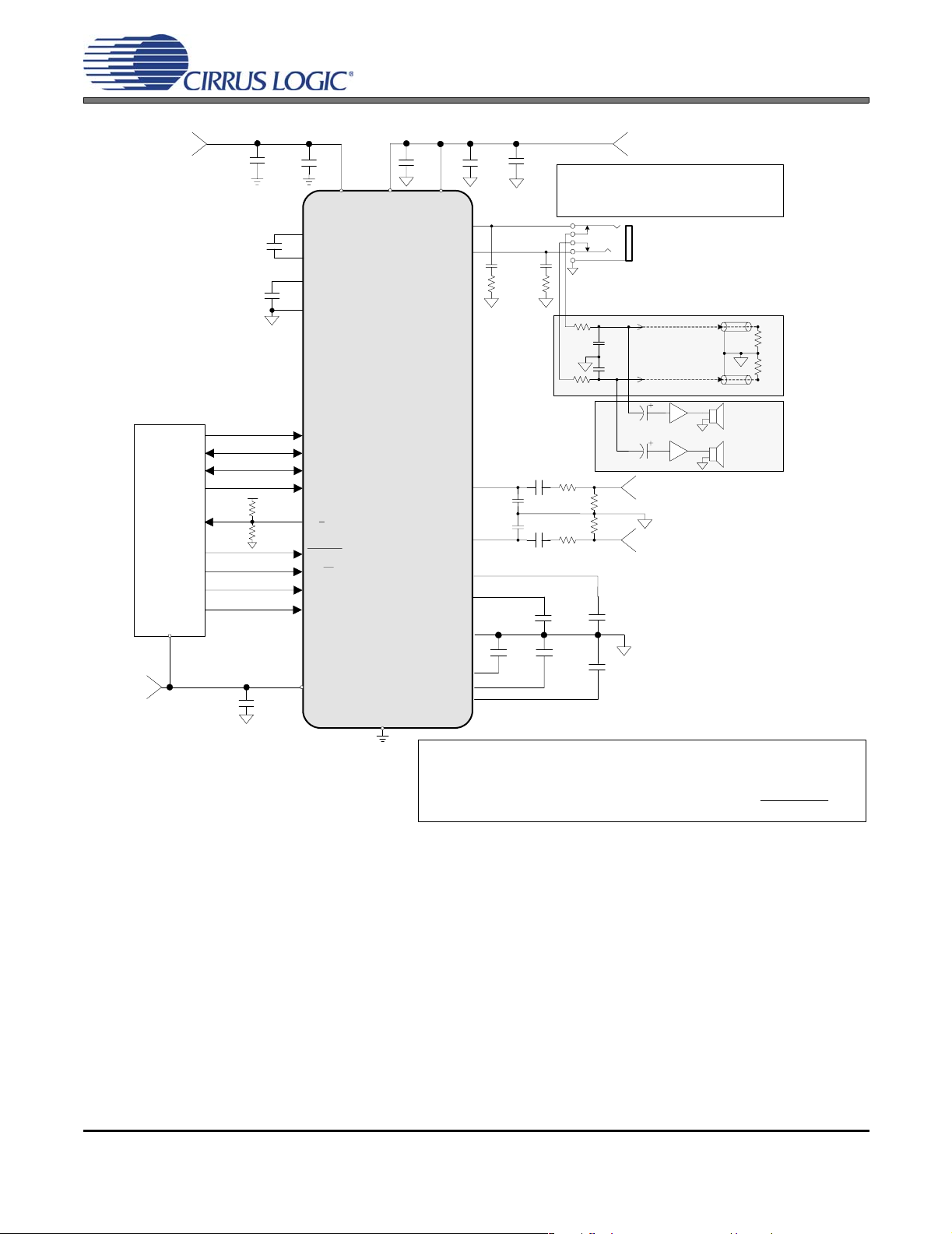
2. TYPICAL CONNECTION DIAGRAMS
+1.8 V o r +2.5 V
* *Use low ESR ceramic capacitors.
Note 2 :
For best response to Fs/2 :
C
This circuitry is intended fo r applications where the
CS42L51 connects directly to an unbalanced output of the
device. For internal routing applications please see the
DAC Analog Output Cha racteristics section for loading
limitations.
Note 5 :
Larger capacitors, such as 1.5 µF, improves the charge
pump performance (and subsequent THD+N) at the full
scale output power achieved with gain (G) settings
greater than default.
470×+
R
ext
=
()
RFs
π
ext
1.5 µF
See Note 5
1.5 µF
4704
**
**
1 µF
1 µF
1 µF
Digital Audio
Processor
2 k
2 k
Ω
+1.8 V, +2.5 V
See Note 1
or +3.3 V
Note 1:
Resistors are required for I²C
control port operation
Ω
0.1 µF
0.1 µF
**
**
VD
FLYP
FLYN
VSS_HP
GND_HP
CS42L51
MCLK
SCLK
LRCK
SDIN
SDOUT
RESET
SCL/CCLK
SDA/CDIN
AD0/CS
VL
DGND
0.1 µF
VA
AIN3B/MICIN2
ADC_FILT+
DAC_FILT+
VA_HP
AOUTB
AOUTA
AIN1A
AIN1B
AIN2A
AIN2B
BIAS1
MICIN1
AIN3A
BIAS2
AGND
AFILTA
AFILTB
0.1 µF
1800 pF
1800 pF
1800 pF
1800 pF
**
VQ
* Capacitors must be C0G or equivalent
0.022 µF
51.1 Ω
*
*
*
*
1 µF
0.1 µF
1000 pF
1 µF
1 µF
1 µF
1 µF
1 µF
See Note 4
+1.8 V or +2.5 V
Note 4:
Series resistance in the path of the power supplies must
be avoided. Any voltage drop on VA_HP will dir ectly
impact the negative charge pump supply (VSS_HP) and
result in clipping on the audio output .
Headphone Out
Left & Right
470
Ω
C
Line Level Out
Left & Right
See Note 2
C
470
Ω
Speaker Driver
Left Analog Input 1
100 Ω
100 kΩ
100 kΩ
100 Ω
100 Ω
100 Ω
100 kΩ
R
L
Note 3: The value of RL is dictated
by the microphone cartridge.
1 µF
1000 pF
Right Analog Input 1
Left Analog Input 2
100 kΩ
100 kΩ
Right Analog Input 2
Microphone Input
Microphone Bias
See Note 3
10 µF
1 µF
CS42L51
R
ext
R
ext
Figure 1. Typical Connection Diagram (Software Mode)
10 DS679A2
CS42L51
+1.8V or +2.5V
* *Use low ESR ceramic capacitors.
Digital Audio
Processor
+1.8V, 2.5 V
or +3.3V
1 µF
1 µF
1 µF
VL
0.1 µF
0.1 µF
**
**
VD
FLYP
FLYN
VSS_HP
GND_HP
MCLK
SCLK
LRCK
SDIN
SDOUT/
M/S
RESET
I²S/LJ
MCLKDIV2
DEM
VL
VA
CS42L51
DGND
0.1 µF
VA_HP
AOUTB
AOUTA
AIN1A
AIN1B
0.1 µF
1800 pF
1800 pF
0.022 µF
51.1 Ω
*
*
See Note 4
1 µF
Note 4:
Series resistance in the path of the power supplies (typically
used for added filtering) must be avoided. Any voltage drop
on VA_HP will directly impact the negative charge pump
supply (VSS_HP) and result in clipping on the audio output .
470Ω
470Ω
100 Ω
1 µF
100 Ω
1 µF
+1.8V or +2.5V
C
Line Level Out
Left & Right
See Note 2
C
Speaker Driver
Left Analog Input 1
100 kΩ
100 kΩ
Right Analog Input 1
Headphone Out
Left & Right
R
ext
R
ext
ADC_FILT+
DAC_FILT+
AGND
AFILTA
AFILTB
VQ
1 µF
**
* Capacitors must be C0G or equivalent
1000 pF
1000 pF
10 µF
1 µF
Note 2 :
This circuitry is intended for applications where the CS 42L51 connects directly to an unbalanced output of the device . For
internal routing applications please see the DAC Analog Output Characteristics section for loading limitations .
470×+
R
ext
=
For best response to Fs/2 :
C
()
RFs
π
ext
4704
Figure 2. Typical Connection Diagram (Hardware Mode)
DS679A2 11
CS42L51
3. CHARACTERISTIC AND SPECIFICATION TABLES
(All Min/Max characteristics and specifications are guaranteed over the Specified Operating Conditions. Typical
performance characteristics and spe cif icat ion s ar e de ri ved from measurements taken at nominal supply voltages
and T
= 25° C.)
A
SPECIFIED OPERATING CONDITIONS
(AGND=DGND=0 V, all voltages with respect to ground.)
Parameters Symbol Min Nom Max Units
DC Power Supply (Note 1)
Analog Core VA 1.71
2.37
Headphone Amplifier VA_HP 1.71
2.37
Digital Core VD 1.71
2.37
Serial/Control Port Interface VL 1.71
2.37
3.14
Ambient Temperature
Commercial - CNZ
Automotive - DNZ
T
A
-10
-40
1.8
2.5
1.8
2.5
1.8
2.5
1.8
2.5
3.3
1.89
2.63
1.89
2.63
1.89
2.63
1.89
2.63
3.47
-
-
+70
+85
V
V
V
V
V
V
V
V
V
°C
°C
ABSOLUTE MAXIMUM RATINGS
(AGND = DGND = 0 V; all voltages with respect to ground.)
Parameters Symbol Min Max Units
DC Power Supply Analog
Digital
Serial/Control Port Interface
Input Current (Note 2) I
Analog Input Voltage (Note 3)
Digital Input Voltage
(Note 3))
Ambient Operating Temperature Commercial - CNZ
(power applied) Automotive - DNZ
Storage Temperature T
WARNING:Operation at or beyond these limits may result in permanent damage to the device. Normal operation
is not guaranteed at these extremes.
Notes:
1. The device will operate properly over the full range of the analog, headphone amplifier, digital core and
serial/control port interface supplies.
2. Any pin except supplies. Transient currents of up to ±100 mA on the analog input pins will not cause
SCR latch-up.
3. The maximum over/under voltage is limited by the input current.
VA, VA_HP
VD
VL
in
V
IN
V
IND
T
A
stg
-0.3
-0.3
-0.3
-±10mA
3.0
3.0
4.0
V
V
V
AGND-0.7 VA+0.7 V
-0.3 VL+ 0.4 V
-20
-50
-65 +150 °C
+85
+95
°C
°C
12 DS679A2

CS42L51
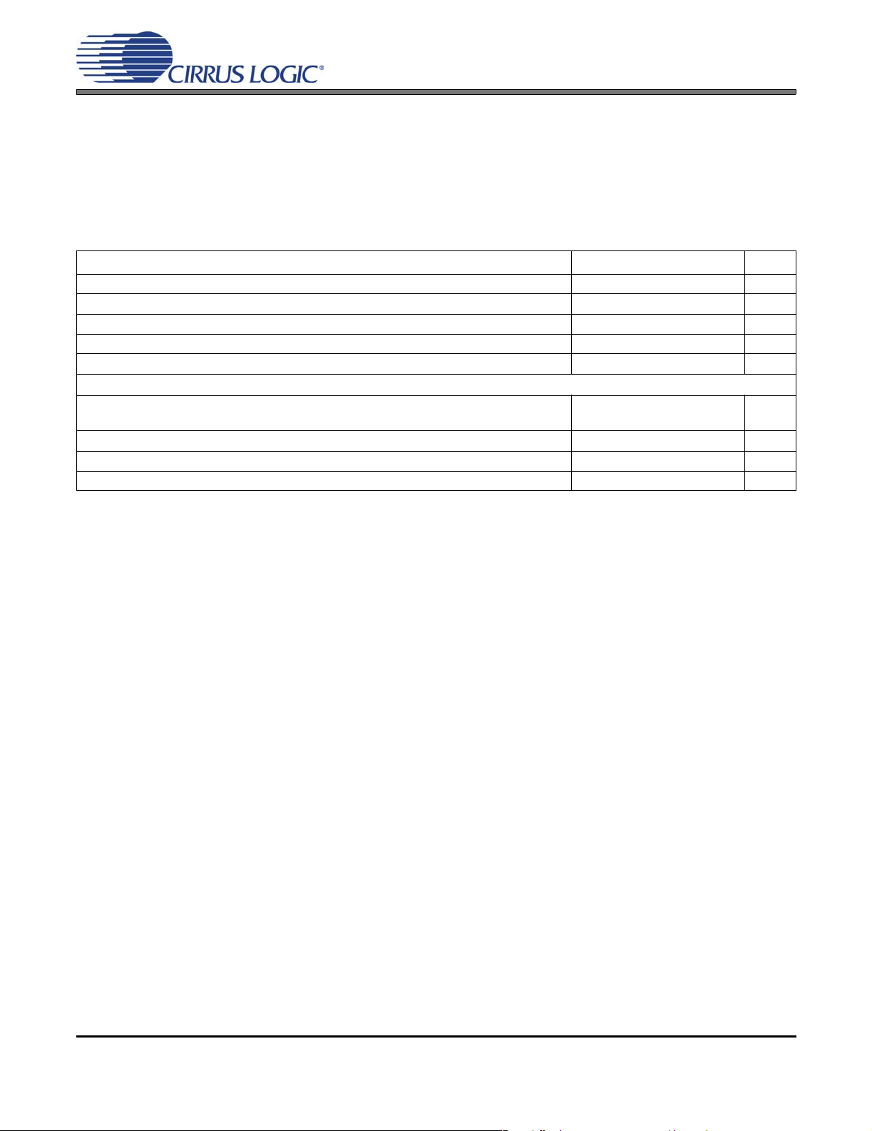
ANALOG INPUT CHARACTERISTICS (COMMERCIAL - CNZ)
(Test Conditions (unless otherwise specified): All supplies = VA = 2.5 V and 1.8 V; Input sine wave (relative to digital full-scale): 1 kHz through passive input filter; Measurement Bandwidth is 10 Hz to 20 kHz unless otherwise
specified. Sample Frequency = 48 kHz)
VA = 2.5V VA = 1.8V
Parameter (Note 4)
Analog In to ADC (PGA bypassed)
Dynamic Range A-weighted
unweighted9390
Total Harmonic Distortion + Noise -1 dBFS
-20 dBFS
-60 dBFS
Analog In to PGA to ADC
Dynamic Range
PGA Setting: 0 dB A-weighted
unweighted9289
PGA Setting: +12 dB A-weighted
unweighted8582
Total Harmonic Distortion + Noise
PGA Setting: 0 dB -1 dBFS
-60 dBFS
PGA Setting: +12 dB -1 dBFS - -85 -79 - -83 -77 dB
Analog In to MIC Pre-Amp(+16 dB) to PGA to ADC
Dynamic Range
PGA Setting: 0 dB A-weighted
unweighted
Total Harmonic Distortion + Noise
PGA Setting: 0 dB -1 dBFS - -76 - - -74 - dB
Analog In to MIC Pre-Amp(+32 dB) to PGA to ADC
Dynamic Range
PGA Setting: 0 dB A-weighted
unweighted
Total Harmonic Distortion + Noise
PGA Setting: 0 dB -1 dBFS - -74 - - -71 - dB
Other Characteristics
DC Accuracy
Interchannel Gain Mismatch - 0.1 - - 0.1 - dB
Gain Drift - ±100 - - ±100 - ppm/°
Input
Interchannel Isolation - 90 - - 90 - dB
DAC Isolation (Note 5) -70- -70-dB
Full-scale Input Voltage (x•VA) (Note 7) 0.70•VA 0.72•VA 0.75•VA 0.70•VA 0.72•VA 0.75•VA Vpp
Input Impedance (Note 6) ADC
PGA
MIC
Min Typ Max Min Typ Max Unit
18
40
50
99
96
-
-
-
-
-
-
-
-
-
-86
-76
-36
98
95
91
88
-88
-35
86
83
78
74
-
-
-
-80
-82
-
-
-
-
-
-
-
-
-
-
-
-
-
-
-
-
90
87
89
86
82
79
18
40
50
96
93
-
-
-
-
-
-
-
-
-
-84
-73
-33
95
92
88
85
-86
-32
83
80
75
71
-
-
-
-78
-80
-
-
-
-
-
-
-
-
-
-
-
-
-
-
-
-
dB
dB
dB
dB
dB
dB
dB
dB
dB
dB
dB
dB
dB
dB
dB
C
Ω
k
kΩ
kΩ
DS679A2 13

CS42L51
ANALOG INPUT CHARACTERISTICS (AUTOMOTIVE - DNZ)
(Test Conditions (unless otherwise specified): All supplies = VA = 2.5 V and 1.8 V; Input sine wave (relative to fullscale): 1 kHz through passive input filter; Measurement Bandwidth is 10 Hz to 20 kHz unless otherwise specified.
Sample Frequency = 48 kHz)
VA = 2.5V VA = 1.8V
Parameter (Note 4)
Analog In to ADC
Dynamic Range A-weighted
unweighted9178
Total Harmonic Distortion + Noise -1 dB
-20 dB
-60 dB
Analog In to PGA to ADC
Dynamic Range
PGA Setting: 0 dB A-weighted
unweighted9087
PGA Setting: +12 dB A-weighted
unweighted8380
Total Harmonic Distortion + Noise
PGA Setting: 0 dB -1 dB
-60 dB
PGA Setting: +12 dB -1 dB - -85 -77 - -83 -75 dB
Analog In to MIC Pre-Amp(+16 dB) to PGA to ADC
Dynamic Range
PGA Setting: 0 dB A-weighted
unweighted
Total Harmonic Distortion + Noise
PGA Setting: 0 dB -1 dB - -76 - - -74 - dB
Analog In to MIC Pre-Amp(+32 dB) to PGA to ADC
Dynamic Range
PGA Setting: 0 dB A-weighted
unweighted
Total Harmonic Distortion + Noise
PGA Setting: 0 dB -1 dB - -74 - - -71 - dB
Other Characteristics
DC Accuracy
Interchannel Gain Mismatch - 0.1 - - 0.1 - dB
Gain Drift - ±100 - - ±100 - ppm/°
Input
Interchannel Isolation - 90 - - 90 - dB
DAC Isolation (Note 5) -70- -70-dB
Full-scale Input Voltage (Note 7) 0.70•VA 0.72•VA 0.75•VA 0.70•VA 0.72•VA 0.75•VA Vpp
Input Impedance (Note 6) ADC
PGA
MIC
Notes:
4. Referred to the typical full-scale voltage.
5. Measured with DAC delivering full-scale output power into 16 Ω.
Min Typ Max Min Typ Max Unit
18
40
50
99
96
-
-
-
-
-
-
-
-
-
-86
-76
-36
98
95
91
88
-88
-35
86
83
78
74
-
-
-
-
-
-78
-
-
-
-
-
-
-80
-
-
-
-
-
-
-
-
88
85
87
84
80
77
18
40
50
96
93
-
-
-
-
-
-
-
-
-
-84
-73
-33
95
92
88
85
-86
-32
83
80
75
71
-
-
-
-
-
-76
-
-
-
-
-
-
-78
-
-
-
-
-
-
-
-
dB
dB
dB
dB
dB
dB
dB
dB
dB
dB
dB
dB
dB
dB
dB
C
Ω
k
kΩ
kΩ
14 DS679A2
CS42L51
Notes:
6. Measured between AINxx and AGND.
7. Full-scale input voltage characteristics for the PGA and Microphone inputs are scaled based on the gain
setting for each.
ADC DIGITAL FILTER CHARACTERISTICS
Parameter (Note 8) Min Typ Max Unit
Passband (Frequency Response) to -0.1 dB corner 0 - 0.4948 Fs
Passband Ripple -0.09 - 0 dB
Stopband 0.6677 - - Fs
Stopband Attenuation 48.4 - - dB
Total Group Delay - 2.7/Fs - s
High-Pass Filter Characteristics
Frequency Response -3.0 dB
-0.13 dB
Phase Deviation @ 20 Hz - 10 - Deg
Passband Ripple - - 0.17 dB
Filter Settling Time -10
-
-
3.7
24.2
5
/Fs 0 s
-
-
Hz
Hz
Notes:
8. Response is clock dependent and will scale with Fs. Note that the response plots (Figures 33 to 36 on
page 78) have been normalized to Fs and can be de-normalized by multiplying the X-axis scale by Fs.
DS679A2 15
CS42L51
ANALOG OUTPUT CHARACTERISTICS (COMMERCIAL - CNZ)
(Test conditions (unless otherwise specified): Input test signal is a full-scale 997 Hz sine wave; measurement
bandwidth is 10 Hz to 20 kHz; Sample Frequency = 48 kHz; test load R
(see Figure 3), and test load R
= 16 Ω, CL = 10 pF (see Figure 3) for the headphone output. HP_GAIN[2:0] = 011.)
L
= 10 kΩ, CL = 10 pF for the line output
L
Parameter (Note 9)
Min Typ Max
VA = 2.5V
VA = 1.8V
Min Typ Max Unit
RL = 10 kΩ
Dynamic Range
18 to 24-Bit A-weighted
unweighted
16-Bit A-weighted
unweighted
Total Harmonic Distortion + Noise
18 to 24-Bit 0 dB
-20 dB
-60 dB
16-Bit 0 dB
-20 dB
-60 dB
92
89
98
95
-
-
-
-
-
-
-
-
96
93
-86
-75
-35
-86
-73
-33
-80
-
-
-
-
-
-
-
-
-
89
86
95
92
-
-
-
-
-
-
-
-
93
90
-88
-72
-32
-88
-70
-30
-82
-
-
-
-
-
-
-
-
-
dB
dB
dB
dB
dB
dB
dB
dB
dB
dB
RL = 16 Ω
Dynamic Range
18 to 24-Bit A-weighted
unweighted
16-Bit A-weighted
unweighted
Total Harmonic Distortion + Noise
18 to 24-Bit 0 dB
-20 dB
-60 dB
16-Bit 0 dB
-20 dB
-60 dB
Other Characteristics for RL = 16 Ω or 10 k
Output Parameters Modulation Index (MI)
(Note 10) Analog Gain Multiplier (G)
Full-scale Output Voltage (2•G•MI•VA) (Note 10) Refer to Table “Line Output Voltage Characteristics” on
Full-scale Output Power (Note 10) Refer to Table “Headphone Output Power Characteristics” on
Interchannel Isolation (1 kHz) 16 Ω
Interchannel Gain Mismatch - 0.1 0.25 - 0.1 0.25 dB
Gain Drift - ±100 - - ±100 - ppm/°
AC-Load Resistance (R
Load Capacitance (C
) (Note 11) 16 - - 16 - - Ω
L
) (Note 11) - - 150 - - 150 pF
L
Ω
10 kΩ
92
89
-
-
-
-
-
-
-
-
- 0.6787
-
-
98
95
96
93
-75
-75
-35
-75
-73
-33
0.6047
80
95
-
-
-
-
-69
-
-
-
-
-
- - 0.6787
page 18
-
-
89
86
-
-
-
-
-
-
-
-
page 19
-
-
95
92
93
90
-75
-72
-32
-75
-70
-30
0.6047
80
93
-69
-
-
-
-
-
-
-
-
-
-
-
-
dB
dB
dB
dB
dB
dB
dB
dB
dB
dB
Vpp
dB
dB
C
16 DS679A2

CS42L51
ANALOG OUTPUT CHARACTERISTICS (AUTOMOTIVE - DNZ)
(Test conditions (unless otherwise specified): Input test signal is a full-scale 997 Hz sine wave; measurement
bandwidth is 10 Hz to 20 kHz; Sample Frequency = 48 kHz and 96 kHz; test load R
line output (see Figure 3), and test load R
= 16 Ω, CL = 10 pF (see Figure 3) for the headphone output.
L
HP_GAIN[2:0] = 011.)
= 10 kΩ, CL = 10 pF for the
L
Parameter (Note 9)
Min Typ Max
VA = 2.5V
VA = 1.8V
Min Typ Max Unit
RL = 10 kΩ
Dynamic Range
18 to 24-Bit A-weighted
unweighted
16-Bit A-weighted
unweighted
Total Harmonic Distortion + Noise
18 to 24-Bit 0 dB
-20 dB
-60 dB
16-Bit 0 dB
-20 dB
-60 dB
90
87
98
95
-
-
-
-
-
-
-
-
96
93
-86
-75
-35
-86
-73
-33
-78
-
-
-
-
-
-
-
-
-
87
84
95
92
-
-
-
-
-
-
-
-
93
90
-88
-72
-32
-88
-70
-30
-80
-
-
-
-
-
-
-
-
-
dB
dB
dB
dB
dB
dB
dB
dB
dB
dB
RL = 16 Ω
Dynamic Range
18 to 24-Bit A-weighted
unweighted
16-Bit A-weighted
unweighted
Total Harmonic Distortion + Noise
18 to 24-Bit 0 dB
-20 dB
-60 dB
16-Bit 0 dB
-20 dB
-60 dB
Other Characteristics for RL = 16 Ω or 10 k
Output Parameters Modulation Index (MI)
(Note 10) Analog Gain Multip lier (G)
Full-scale Output Voltage (2•G•MI•VA) (Note 10) Refer to Table “Line Output Voltage Characteristics” on
Full-scale Output Power (Note 10) Refer to Table “Headphone Output Power Characteristics” on
Interchannel Isolation (1 kHz) 16 Ω
Interchannel Gain Mismatch - 0.1 0.25 - 0.1 0.25 dB
Gain Drift - ±100 - - ±100 - ppm/°
AC-Load Resistance (R
Load Capacitance (C
) (Note 11) 16 - - 16 - - Ω
L
) (Note 11) - - 150 - - 150 pF
L
Ω
10 kΩ
90
87
-
-
-
-
-
-
-
-
- 0.6787
-
-
98
95
96
93
-75
-75
-35
-75
-73
-33
0.6047
80
95
-
-
-
-
-67
-
-
-
-
-
- - 0.6787
page 18
-
-
87
84
-
-
-
-
-
-
-
-
page 19
-
-
95
92
93
90
-75
-72
-32
-75
-70
-30
0.6047
80
93
-67
-
-
-
-
-
-
-
-
-
-
-
-
dB
dB
dB
dB
dB
dB
dB
dB
dB
dB
Vpp
dB
dB
C
DS679A2 17
CS42L51
LINE OUTPUT VOLTAGE CHARACTERISTICS
Test conditions (unless otherwise specified): Inp ut test signal is a fu ll-scale 997 Hz sine wave; measurement bandwidth is 10 Hz to 20 kHz; Sample Frequency = 48 kHz; test load R
= 10 kΩ, CL = 10 pF (see Figure 3).
L
Parameter
AOUTx Voltage Into RL = 10 k
HP_GAIN[2:0] Analog
Min Typ Max
Ω
VA_HP
VA = 2.5V
VA = 1.8V
Min Typ Max Unit
Gain (G)
000 0.3959 1.8 V - 1.34 - - 0.97 - V
2.5 V - 1.34 - - 0.97 - V
001 0.4571 1.8 V - 1.55 - - 1.12 - V
2.5 V - 1.55 - - 1.12 - V
010 0.5111 1.8 V - 1.73 - - 1.25 - V
2.5 V - 1.73 - - 1.25 - V
011 (default) 0.6047 1.8 V - 2.05 - 1.41 1.48 1.55 V
2.5 V 1.95 2.05 2.15 - 1.48 - V
100 0.7099 1.8 V - 2.41 - - 1.73 - V
2.5 V - 2.41 - - 1.73 - V
101 0.8399 1.8 V - 2.85 - 2.05 V
2.5 V - 2.85 - - 2.05 - V
110 1.0000 1.8 V - 3.39 - - 2.44 - V
2.5 V - 3.39 - - 2.44 - V
1 11 1.1430 1.8 V (See (Note 12) 2.79 V
2.5 V - 3.88 - - 2.79 - V
pp
pp
pp
pp
pp
pp
pp
pp
pp
pp
pp
pp
pp
pp
pp
pp
18 DS679A2
CS42L51
HEADPHONE OUTPUT POWER CHARACTERISTICS
Test conditions (unless otherwise specified): Input test signal is a full-scale 997 Hz sine wave; measurement bandwidth is 10 Hz to 20 kHz; Sample Frequency = 48 kHz; test load R
= 16 Ω, CL = 10 pF (see Figure 3).
L
Parameter
AOUTx Power Into RL = 16
HP_GAIN[2:0] Analog
Min Typ Max
Ω
VA_HP
VA = 2.5V
VA = 1.8V
Min Typ Max Unit
Gain (G)
000 0.3959 1.8 V - 14 - - 7 - mW
2.5 V - 14 - - 7 - mW
001 0.4571 1.8 V - 19 - - 10 - mW
2.5 V - 19 - - 10 - mW
010 0.5111 1.8 V - 23 - - 12 - mW
2.5 V - 23 - - 12 - mW
011 (default) 0.6047 1.8 V (Note 12) -17 -mW
2.5 V - 32 - - 17 - mW
100 0.7099 1.8 V (Note 12) -23 -mW
2.5 V - 44 - - 23 - mW
101 0.8399 1.8 V (Note 10)) See Figure 28 on
mW
rms
rms
rms
rms
rms
rms
rms
rms
rms
rms
rms
page 72
2.5 V -32 -mW
110 1.0000 1.8 V (Note 10, 12) See Figures 28 and 29 on page 72 mW
2.5 V mW
111 1.1430 1.8 V mW
2.5 V mW
rms
rms
rms
rms
rms
Notes:
9. One-half LSB of triangular PDF dither is added to data.
10. Full-scale output voltage and power is determined by the gain setting, G, in register “Headphone Analog
Gain (HP_GAIN[2:0])” on page 54. High gain settings at certain VA and VA_HP supply levels may
cause clipping when the audio signal approaches full-scale, maximum power output, as shown in
Figures 28 - 31 on page 73.
11. See Figure 3. R
quired for the internal op-amp's stability and signal integrity. In this circuit topology, C
and CL reflect the recommended minimum resistance and maximum capacitance re-
L
will effectively
L
move the band-limiting pole of the amp in the output stage. Increasing this value beyond the recommended 150 pF can cause the internal op-amp to become unstable.
12. VA_HP settings lower than VA reduces the headroom of the h eadphone amplifier. As a resu lt, the DAC
may not achieve the full THD+N performance at full-scale output voltage and power.
AOUTx
51 Ω
0.022 µF
AGND
C
L
Figure 3. Headphone Output Test Load
R
L
DS679A2 19
CS42L51
COMBINED DAC INTERPOLATION & ON-CHIP ANALOG FILTER RESPONSE
Parameter (Note 13))MinTypMaxUnit
Frequency Response 10 Hz to 20 kHz -0.01 - +0.08 dB
Passband to -0.05 dB corner
to -3 dB corner00
StopBand 0.5465 - - Fs
StopBand Attenuation (Note 14) 50 - - dB
Group Delay - 9/Fs - s
De-emphasis Error Fs = 32 kHz
Fs = 44.1 kHz
Fs = 48 kHz
-
-
-
-
-
-
-
-
0.4780
0.4996
+1.5/+0
+0.05/-0.25
-0.2/-0.4
Fs
Fs
dB
dB
dB
Notes:
13. Response is clock dependent and will scale with Fs. Note that the response plots (Figures 35 and 36 on
page 78) have been normalized to Fs and can be de-normalized by multiplying the X-axis scale by Fs.
14. Measurement Bandwidth is from Stopband to 3 Fs.
SWITCHING SPECIFICATIONS - SERIAL PORT
(Inputs: Logic 0 = DGND, Logic 1 = VL, SDOUT C
LOAD
= 15 pF.)
Parameters Symbol Min Max Units
RESET pin Low Pulse Width (Note 15)
MCLK Frequency 1.024 38.4 MHz
MCLK Duty Cycle (Note 16) 45 55 %
1-ms
Slave Mode
Input Sample Rate (LRCK) Quarter-Speed Mode
Half-Speed Mode
Single-Speed Mode
Double-Speed Mode
LRCK Duty Cycle 45 55 %
SCLK Frequency 1/t
SCLK Duty Cycle 45 55 %
LRCK Setup Time Before SCLK Rising Edge t
LRCK Edge to SDOUT MSB Output Delay t
SDOUT Setup Time Before SCLK Rising Edge t
SDOUT Hold Time After SCLK Rising Edge t
SDIN Setup Time Before SCLK Rising Edge t
SDIN Hold Time After SCLK Rising Edge t
F
s
F
s
F
s
F
s
P
s(LK-SK)
d(MSB)
s(SDO-SK)
h(SK-SDO)
s(SD-SK)
h
4
8
4
50
-64•FsHz
40 - ns
-40ns
30 - ns
30 - ns
20 - ns
20 - ns
12.5
25
50
100
kHz
kHz
kHz
kHz
20 DS679A2
CS42L51
LRCK
//
t
s(LK-SK)
//
t
P
//
SCLK
//
SDOUT
SDIN
t
d(MSB)
t
s(SD-SK)
MSB
MSB
t
h(SK-SDO)
//
//
t
//
//
t
s(SDO-SK)
MSB-1
h
MSB-1
Figure 4. Serial Audio Interface Slave Mode Timing
Parameters Symbol Min Max Units
Master Mode (Note 17)
Output Sample Rate (LRCK) All Speed Modes F
s
LRCK Duty Cycle 45 55 %
SCLK Frequency 1/t
P
SCLK Duty Cycle 45 55 %
SCLK Rising Edge to SDOUT Output Delay t
LRCK Edge to SDOUT MSB Output Delay t
SDOUT Setup Time Before SCLK Rising Edge t
SDOUT Hold Time After SCLK Rising Edge t
SDIN Setup Time Before SCLK Rising Edge t
SDIN Hold Time After SCLK Rising Edge t
d
d(MSB)
s(SDO-SK)
h(SK-SDO)
s(SD-SK)
h
-Hz
- 64•F
-s
MCLK
----------------128
1
-----------------
MCLK
Hz
s
-40ns
30 - ns
30 - ns
20 - ns
20 - ns
Notes:
15. After powering up the CS42L51, RESET should be held low after the power supplies and clocks are se ttled.
16. See “Example System Clock Frequencies” on page 75 for typical MCLK frequencies.
17. See “Master” on page 38.
//
LRCK
//
t
P
//
SCLK
//
t
d(MSB)
SDOUT
t
s(SD-SK)
SDIN
Figure 6. Serial Audio Interface Master Mode Timing
DS679A2 21
MSB
MSB
t
h(SK-SDO)
//
//
t
//
//
t
s(SDO-SK)
MSB-1
h
MSB-1
SWITCHING SPECIFICATIONS - I²C CONTROL PORT
(Inputs: Logic 0 = DGND, Logic 1 = VL, SDA CL=30pF)
Parameter Symbol Min Max Unit
SCL Clock Frequency f
RESET Rising Edge to Start
Bus Free Time Between Transmissions t
Start Condition Hold Time (prior to first clock pulse) t
Clock Low time t
Clock High Time t
Setup Time for Repeated Start Condition t
SDA Hold Time from SCL Falling (Note 18) t
SDA Setup time to SCL Rising t
Rise Time of SCL and SDA t
Fall Time SCL and SDA t
Setup Time for Stop Condition t
Acknowledge Delay from SCL Falling t
Notes:
18. Data must be held for sufficient time to bridge the transition time, tfc, of SCL.
scl
t
irs
buf
hdst
low
high
sust
hdd
sud
rc
fc
susp
ack
CS42L51
- 100 kHz
500 - ns
4.7 - µs
4.0 - µs
4.7 - µs
4.0 - µs
4.7 - µs
0-µs
250 - ns
-1µs
- 300 ns
4.7 - µs
300 1000 ns
RST
SDA
SCL
t
irs
Stop Start
t
buf
Repeated
Start
t
t
hdst
low
t
high
t
hdd
t
sud
t
sust
Figure 7. Control Port Timing - I²C
t
hdst
Stop
t
f
t
r
t
susp
22 DS679A2
SWITCHING CHARACTERISTICS - SPI CONTROL PORT
(Inputs: Logic 0 = DGN D, Lo gic 1 = VL)
Parameter Symbol Min Max Units
CCLK Clock Frequency f
RESET Rising Edge to CS Falling
CS
Falling to CCLK Edge t
CS High Time Between Transmissions t
CCLK Low Time t
CCLK High Time t
CDIN to CCLK Rising Setup Time t
CCLK Rising to DATA Hold Time (Note 19) t
Rise Time of CCLK and CDIN (Note 20) t
Fall Time of CCLK and CDIN (Note 20) t
Notes:
19. Data must be held for sufficient time to bridge the transition time of CCLK.
20. For f
<1 MHz.
sck
t
sck
srs
css
csh
scl
sch
dsu
dh
r2
f2
20 - ns
20 - ns
1.0 - µs
66 - ns
66 - ns
40 - ns
15 - ns
CS42L51
06.0MHz
-100ns
-100ns
RST
CS
CCLK
CDIN
t
srs
t
t
sch
css
t
scl
t
f2
t
t
dh
dsu
Figure 8. Control Port Timing - SPI Format
t
csh
t
r2
DS679A2 23
CS42L51
DC ELECTRICAL CHARACTERISTICS
(AGND = 0 V; all voltages with respect to ground.)
Parameters Min Typ Max Units
VQ Characteristics
Nominal Voltage
Output Impedance
DC Current Source/Sink
DAC_FILT+ Nominal Voltage
(Note 21)
ADC_FILT+ Nominal Voltage
-
-
-
-
-
VSS_HP Characteristics
Nominal Voltage
DC Current Source
-
-
MIC BIAS Characteristics
Nominal Voltage MICBIAS _LVL[1:0] = 00
MICBIAS_LVL[1:0] = 01
MICBIAS_LVL[1:0] = 10
MICBIAS_L VL[1:0] = 11
DC Current Source
Power Supply Rejection Ratio (PSRR) 1 kHz
Power Supply Rejection Ratio (PSRR) (Note 22) 1 kHz - 60 - dB
-
-
-
-
-
-
0.5•VA
23
-
VA
VA
-0.8•(VA_HP) -
0.8•VA
0.7•VA
0.6•VA
0.5•VA
-
50
-
-
10
-
-
10
-
-
-
-
1
-
V
kΩ
µA
V
V
V
µA
V
V
V
V
mA
dB
Notes:
21. The DC current draw represents the allowed current draw from the VQ pin due to typical leakage
through electrolytic de-coupling capacitors.
22. Valid with the recommended capacitor values on DAC_FILT+, ADC_FILT+ and VQ. In cr ea sin g t he capacitance will also increase the PSRR.
DIGITAL INTERFACE SPECIFICATIONS & CHARACTERISTICS
Parameters (Note 23) Symbol Min Max Units
Input Leakage Current I
Input Capacitance -10pF
1.8 V - 3.3 V Logic
High-Level Output Voltage
Low-Level Output Voltage (I
High-Level Input Voltage V
Low-Level Input Voltage V
(IOH = -100 µA) V
= 100 µA) V
OL
in
OH
OL
IH
IL
23. See “Digital I/O Pin Characteristics” on page 9 for serial and control port power rails.
-±10µA
VL - 0.2 - V
-0.2V
0.65•VL - V
- 0.35•VL V
24 DS679A2
CS42L51
POWER CONSUMPTION
See (Note 24).
Power Ctl. Registers Typical Current (mA)
02h 03h
Total
Power
Operation
1
(Note 25)
Off
2 Standby (Note 26) xxxxxx1xxx1.8 0 0.01 0.02 0 0.05
3 Mono Record ADC11111001111.8 0 1.85 2.03 0.03 7.05
PGA to ADC11101001111.8 0 2.35 2.03 0.03 7.95
MIC to PGA to ADC
(with Bias)
MIC to PGA to ADC
(no Bias)
4 Stereo Record ADC11110001111.8 0 2.69 2.12 0.03 8.72
PGA to ADC11000001111.8 0 3.65 2.12 0.03 10.45
MIC to PGA to ADC
(no Bias)
5 Mono Playback 10111101111.8 1.66 1.40 2.35 0.01 9.74
6 Stereo Playback 00111101111.8 2.77 2.05 2.35 0.01 12.93
7 Mono Record & Playback
PGA in (no MIC) to Mono Out
8 Phone Monitor
MIC (w/bias) in to Mono Out
9 Stereo Record & Playback
PGA in (no MIC) to Stereo Out
PDN_DACB
PDN_DACA
PDN_PGAB
PDN_PGAA
PDN_ADCB
PDN_ADCA
PDN
PDN_MICB
xxxxxxxxxx1.8 0 0 0 0 0
11101001001.8 0 3.67 2.05 0.03 10.36
11101001011.8 0 3.27 2.03 0.03 9.61
11000000011.8 0 5.48 2.11 0.03 13.73
10101001111.8 1.66 3.63 2.73 0.03 14.49
10101001001.8 1.66 4.95 2.75 0.03 16.90
00000001111.8 2.77 5.59 2.82 0.03 20.18
V
PDN_MICA
VA_HP VA VDVL(Note 27)
PDN_MICBIAS
2.5 0 0 0 0 0
2.5 0 0.01 0.03 0 0.10
2.5 0 2.07 3.05 0.05 12.94
2.5 0 2.58 3.08 0.05 14.29
2.5 0 3.95 3.09 0.05 17.71
2.5 0 3.52 3.08 0.05 16.62
2.5 0 2.93 3.18 0.04 15.40
2.5 0 3.91 3.17 0.04 17.84
2.5 0 5.76 3.17 0.04 22.45
2.5 2.03 1.71 3.48 0.02 18.08
2.5 3.21 2.50 3.49 0.02 23.02
2.5 2.03 4.16 4.08 0.05 25.79
2.5 2.03 5.52 4.08 0.05 29.20
2.5 3.21 6.28 4.19 0.04 34.30
(mW
rms
)
Notes:
24. Unless otherwise noted, test conditions are as follows: All zeros input, slave mode, sample rate =
48 kHz; No load. Digital (VD) and logic (VL) supply current will vary depending on speed mode and master/slave operation.
25. RESET
26. RESET
pin 25 held LO, all clocks and data lines are held LO.
pin 25 held HI, all clocks and data lines are held HI.
27. VL current will slightly increase in master mode.
DS679A2 25

4. APPLICATIONS
4.1 Overview
4.1.1 Architecture
The CS42L51 is a highly integrated, low power, 24-bit au dio CODEC comprised of stereo analog-to-digital
converters (ADC), and stereo digital-to-analog converters (DAC) designed using multi-bit delta-sigma
techniques. The DAC operates at an oversampling ratio of 128Fs and the ADC operates at 64Fs, where
Fs is equal to the system sample rate. The different clock rates ma ximize power savings while maintaining
high performance. The CODEC operates in one of four sample rate speed modes: Quarter, Half, Single
and Double. It accepts and is capable of generating serial port clocks (SCLK, LRCK) derived from an input
Master Clock (MCLK).
4.1.2 Line & MIC Inputs
The analog input portion of the CODEC allows selection from and configuration of multiple combinations
of stereo and microphone (MIC) sources. Six line inputs with configuration for two MIC inputs (or one MIC
input with common mode rejection), two MIC bias outputs and independent channel control (including a
high-pass filter disable function) are available. A Programmable Gain Amplifier (PGA), MIC boost, and Automatic Level Control (ALC), with noise gate settings, provide analog gain and adjustment. Digital volume
controls, including gain, boost, attenuation and inversion are also available.
CS42L51
4.1.3 Line & Headphone Outputs
The analog output portion of the CODEC includes a headphone amplifier capable of driving headphone
and line-level loads. An on-chip charge pump creates a negative headphone supply allowing a full-scale
output swing centered around groun d. Th is elim in at es the need for large DC-Blocking capacitors and allows the amplifier to deliver more power to headphone loads at lower supply voltages. Eigh t gain settings
for the headphone amplifier are available.
4.1.4 Signal Processing Eng ine
A signal processing engine is available to process se rial input d ata (PCM) and ADC data before output to
the DAC. The ADC and PCM data have independent volume controls and mixi ng functions such as mono
mixes and left/right channel swaps. A Tone Control provides bass and treble at four selectable corner frequencies. An automatic level control provides limiting capabilities at programmable attack and release
rates, maximum thresholds and soft ramping. A 15/50µs de-emphasis filter is also available at a 44.1 kHz
sample rate.
4.1.5 Beep Generator
A beep may be generated internally at select frequencies across approximately two octave major scales
and configured to occur continuously, periodically or at single time interva ls controlled by the user. Volume
may be controlled independently.
4.1.6 Device Control (Hardware or Software Mode)
In software mode, all functions and features may be controlled via a two-wire I²C or three-wire SPI con trol
port interface. In hardware mode, a limited fea tu re set may be controlled via stand-alone control pins.
4.1.7 Power Management
Two software mode control registers provide independent power down control of the ADC, DAC, PGA,
MIC pre-amp and MIC bias, allowing operation in select applications with minimal power consumption.
26 DS679A2
CS42L51
4.2 Hardware Mode
A limited feature-set is available when the CODEC powers up in hardware mode (see “Recommended Power-Up
Sequence” on page 40) and may be controlled via stand-alone control pins. Table 2 shows a list of functions/fea-
tures, the default configuration and the associated stand-alone control available.
Hardware Mode Feature/Function Summary
Feature/Function Default Configuration Stand-Alone Control Note
Power Control CODEC
PGAx
ADCx
DACx
MIC Bias
MICx Pre-amplifier
Auto Detect
Speed Mode Serial Port Slave
Serial Port Master
MCLK Divide
Serial Port Master / Slave Selection
Interface Control ADC
DAC
ADC Volume & Gain Digital Boost
Soft Ramp
Zero Cross
Invert
PGAx
Attenuator
ALC
Noise Gate
ADCx High-Pass Filter
ADCx High-Pass Filter Freeze
Line/MIC Input Select
DAC Volume & Gain HP Gain
AOUTx Volume
Invert
Soft Ramp
Zero Cross
Ramp
DAC De-Emphasis
Signal Processing Engine (SPE) MIX
Beep
Tone Control
Peak Detect & Limiter
Data Selection
Channel Mix ADC
DAC
Charge Pump Frequency
Table 2. Hardware Mode Feature Summary
Powered Up
Powered Up
Powered Up
Powered Up
Powered Down
Powered Down
Enabled -
Auto-Detect Speed Mode
Single-Speed Mode
(Selectable)
“MCLKDIV2” pin 2
(Selectable) “M/S” pin 29
(Selectable) “I²S/LJ” pin 3
Disabled
Disabled
Disabled
Disabled
0 dB
0 dB
Disabled
Disabled
Enabled
Continuous DC Subtraction
AIN1A to PGAA
AIN1B to PGAB
G = 0.6047
0 dB
Disabled
Enabled
Disabled
Disabled
(Selectable)
“DEM” pin 4
Disabled
Disabled
Disabled
Disabled
Data Input (PCM) to DAC -
ADCA = L; ADCB = R
PCMA = L; PCMB = R
(64xFs)/7 -
-
-
-
-
-
-
-
-
-
-
-
see Section 4.5
on page 37
see Section 4.5
on page 37
see Section 4.6
on page 39
-
-
-
-
see Section
4.4.1 on page 33
-
-
-
-
DS679A2 27

4.3 Analog Inputs
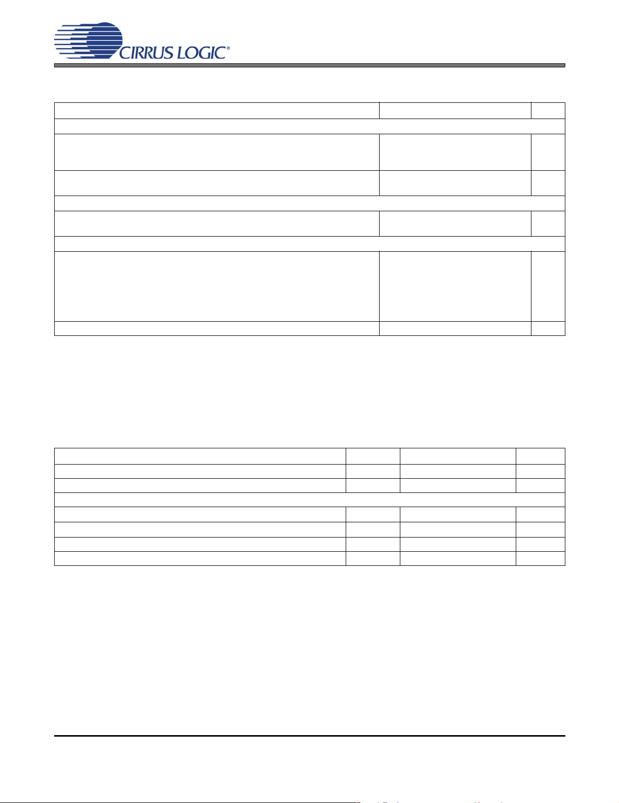
AINxA and AINxB are the analog inputs, internally biased to VQ, that accepts line-level and MIC-level signals, allowing various gain and signal adjustments for each channel.
CS42L51
ADCA_MUTE
ALC_ENA
ALC_ENB
ADCA_ATT[7:0]
0/-96dB
1dB steps
ALC
Attenuator
SOFTA
MUX
DIGMIX
MUX
MICMIX
ADCA_DBOOST
Σ
+20dB
Digital
Boost
ADCA_HPF FREEZE
ADCA_HPF ENABLE
ALC_ARATE[5:0]
ALC_RRATE[5:0]
ALCA_SRDIS
ALCA_ZCDIS
MAX[2:0]
MIN[2:0]
ALCB_SRDIS
ALCB_ZCDIS
PCM Serial Interface
MUX
MUX
ADCB_DBOOST
+20dB
Digital
Boost
ADCB_HPF FREEZE
ADCB_HPF ENABLE
TO SIGNAL PROCESSING
ENGINE (SPE)
FROM SIGNAL
PROCESSING ENGINE (SPE)
SOFTB
Attenuator
ADCB_MUTE
ADCB_ATT[7:0]
0/-96dB
1dB steps
Figure 9. Analog Input Architecture
4.3.1 Digital Code, Offset & DC Measurement
Noise Gate
PDN_ADCA
Multibit
Oversampling
ADC
INV_ADCA
NG_ALL
NG_EN
THRESH[3:0]
NGDELAY[1:0]
PDN_ADCB
Multibit
Oversampling
ADC
INV_ADCB
PGAA_VOL[5:0]
ADC_SNGVOL
SOFTA
ZCROSSA
+12/-3dB
0.5dB steps
PGA
PDN_PGAA
AINA_MUX[1:0]
MICBIAS_LVL[1:0]
PDN_MICBIAS
PGAB_VOL[5:0]
ADC_SNGVOL
SOFTB
ZCROSSB
+12/-3dB
0.5dB steps
PGA
PDN_PGAB
AINB_MUX[1:0]
MUX
MUX
+16/
32 dB
MICA_BOOST
PDN_MICA
MICBIAS
+16/
32 dB
MICB_BOOST
PDN_MICB
MICBIAS_SEL
AIN1A
AIN2A
AIN3A/ MICIN1
AIN1B
AIN2B/MICBIAS
AIN3B/ MICIN2/
MICBIAS
The ADC output data is in two’s complement binary format. For inputs above positive full-scale or below
negative full-scale, the ADC will output 7FFFFFH or 800000H, respectively and cause the ADC overflow
bit to be set to a ‘1’.
Given the two’s complement format, low-level signals may cause the MSB of the se rial data to periodically
toggle between ‘1’ and ‘0’, poss ibly int roducing noise in to the sys tem as the bit switches back an d fort h.
To prevent this phenomena, a constant DC offset is a dded to th e ser ial d ata brin ging th e low- level sig nal
just above the point at which the MSB would normally toggle, thus reducing the noise introduced.
The CODEC may be used to measure DC voltages by disabling the high-pass filter for the designated
channel. DC levels are measured relative to VQ and will be decoded as positive two’s complement binary
numbers above VQ and negative two’s complement binary numbers below VQ.
Software
Controls:
“Status (Address 20h) (Read Only)” on page 71, “ADC Control (Address 06h)” on page 52.
28 DS679A2

4.3.2 High-Pass Filter and DC Offset Calibration
The high-pass filter continuously subtracts a measure of the DC offset from the output of the decimation
filter. If the high-pass filter is “frozen” during normal operation, the current value of the DC offset for the
corresponding channel is held. It is this DC offset that will continue to be subtracted from the conversion
result. This feature makes it possible to perform a system DC offset calibration by:
1. 1) Running the CODEC with the high-pass filter enable d and the DC offset not “frozen ” until the filte r
settles. See the Digital Filter Characteristics for filter settling time.
2. Freezing the DC offset.
The high-pass filters are controlled using the ADCx_HPFRZ and ADCx_HPFEN bits.
If a particular ADC channel is used to measure DC voltages, the high-pass filter may be disabled using
the ADCx_HPFEN bit.
Software
Controls:
“ADC Control (Address 06h)” on page 52.
4.3.3 Digital Routing
The digital output of the ADC may be internally routed to the signal processing engine fo r playback of analog input signals. Volume to the DAC may be controlled using the ADCMIX[6:0] bits. The serial input data
may also be routed to the ADC serial interface using the DIGMIX bit. This is useful for recording a digital
mix along with the analog input.
Software
Controls:
“ADCx Mixer Volume Control: ADCA (Address 0Eh) & ADCB (Address 0Fh)” on page 58, “Inter-
face Control (Address 04h)” on page 49.
CS42L51
4.3.4 Differential Inputs
The stereo pair inputs act as a single differential input when the MICMIX bit is enabled. This p rovides common mode rejection of noise in digitally intense PCB’s where the microphone signal traverses long traces,
or across long microphone cables as illustrated in Figure 10.
Since the mixer provides a differential combination of the two signals, the potential input mix may exceed
the maximum full-scale input and result in clipping. The level out of the mixer, therefore, is automatically
attenuated 6 dB. Gain may be applied using either the analog PGA o r MIC Pre-amp or the digital ADCMIX
volume control to re-adjust a small signal to desired levels.
The analog inputs may also be used as a differential input pair as illustrated in Figure 11. The two channels are differentially combined when the MICMIX bit is enabled.
4.3.4.1 External Passive Components
The microphone input is internally biased to VQ. Input signals must be AC coupled using external capacitors with values consistent with the desired high-pass filter design. The MICINx input resistance of 50 kΩ
may be combined with an external capacitor of 1 µF to achieve the cutoff frequency defined by the equation,
An electrolytic capacitor must be placed such that the positive terminal is positioned relative to the side with
the greater bias voltage. The MICBIAS voltage level is controlled by the MICBIAS_LVL[1:0] bits.
f
------------------------------------------- 3.1 8Hz==
c
2π 50kΩ()1µ F()
1
DS679A2 29
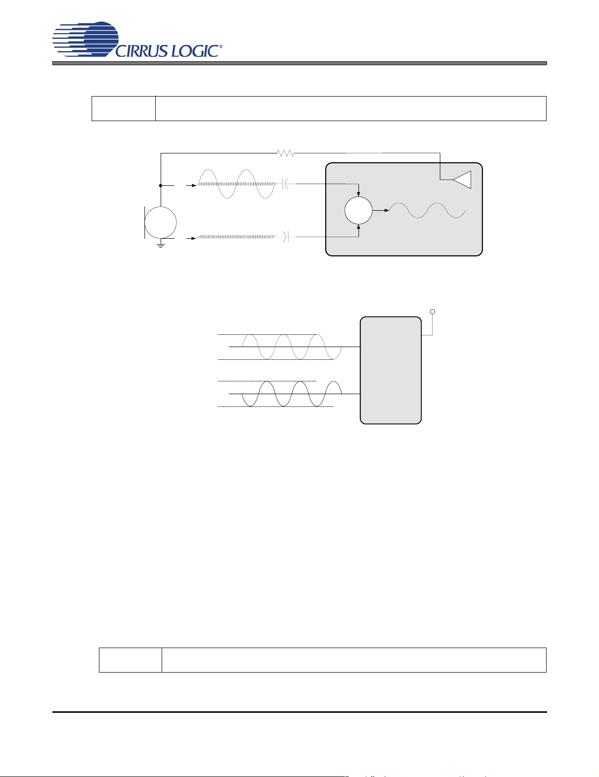
CS42L51
The MICBIAS series resistor must be selected based on the requirements of the particular microphone
used. The MICBIAS output pin is selected using the MICBIAS_SEL bit.
Software
Controls:
“Interface Control (Address 04h)” on page 49, “MIC Control (Ad dress 05h)” on page 51.
MICBIAS
20
MICIN1
//
+
17
Σ
MICIN2
//
Figure 10. MIC Input Mix w/Common Mode Rejection
+
18
2.5 V
2.15 V
1.25 V
0.35 V
2.15 V
1.25 V
0.35 V
Full-Scale Differential Input Level (MICMIX=1)
= (AINxA - AINxB) = 3.6 V
4.3.5 Analog Input Multiplexer
A stereo 4-to-1 analog input multiplexer selects between a line-level input source, or a mic-level input
source, depending on the PDN_PGAx and AINx_MU X[1:0] bit settings. Signals may be routed to or bypassed around the PGA. To conserve power, the PGA’s may be powered down allowing the user to select
from multiple line-level sources and route the stereo signal directly to the ADC. When using the MIC preamp, however, the PGA must be powered up.
Analog input channel B may also be used as an outp ut for the MIC bias volta ge. The MICBIAS_SEL bit
routes the bias voltage to either of two pins. The multiplexer must then select from the remainder of the
two input channels.
The ADC, PGA and MIC pre-amplifier each has an associated input resistance. When selecting between
these paths, the input resistance to the CODEC will change accordingly. Refer to the input resistance
characteristics in the Characteristic and Specification Tables for the input resistance of each path.
Software
Controls:
“Power Control 1 (Address 02h)” on page 47, “MIC Control (Ad dress 05h)” on page 51, “ADCx
Input Select, Invert & Mute (Address 07h)” on page 53.
= 1.27 V
PP
RMS
Figure 11. Differential Input
VA
AINxA
AINxB
30 DS679A2
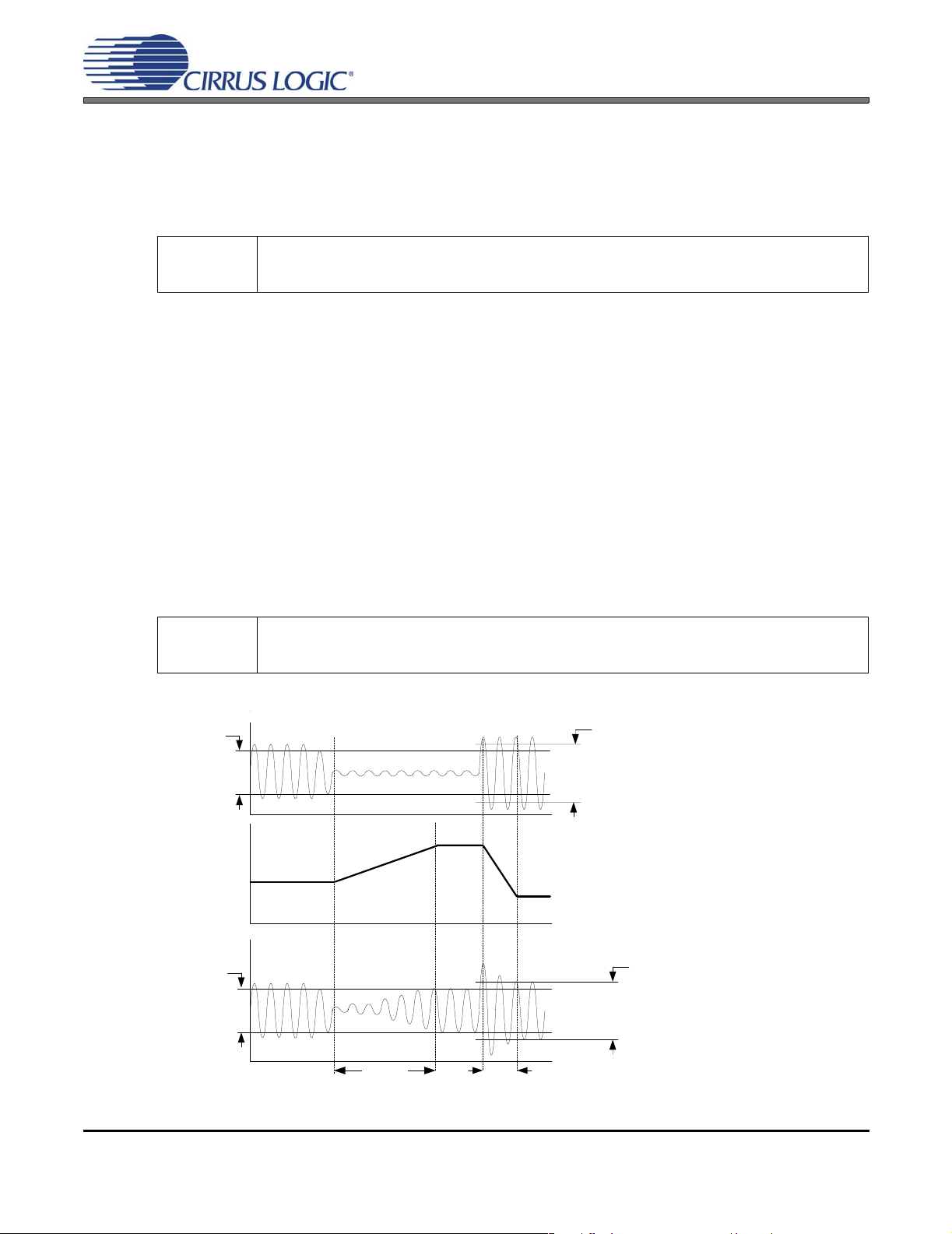
4.3.6 MIC & PGA Gain
The MIC-level input passes through a +16 dB or +32 dB analog gain stage prior to the input multiplexer,
allowing it to be used for microphone level signals without the need for any e x terna l ga in. The PGA mu st
be powered up when using the MIC pre-amp.
The PGA stage provides an additional +12 dB to -3 dB of analog gain in 0.5 dB steps.
Software
Controls:
“Power Control 1 (Address 02h)” on page 47, “ADCx Input Select, Invert & Mute (Address 07h)” on
page 53, “ALCX & PGAX Control: ALCA, PGAA (Address 0Ah) & ALCB, PGAB (Address 0Bh)” on
page 56, “MIC Control (Address 05h)” on page 51.
4.3.7 Automatic Level Control (ALC)
When enabled, the ALC monitors the analog input signal after the digital attenuator, detects when peak
levels exceed the maximum threshold settings and lowers, first, the PGA g ain settings and then increases
the digital attenuation levels at a programmable attack rate and maintains the resulting level below the
maximum threshold.
When input signal levels fall below the minimum threshold, digit al attenuation levels are decreased first
and the PGA gain is then increased at a programmable release rate and maintain s the resulting level below the minimum threshold.
Attack and release rates are affected by the ADC soft ramp/zer o cross settings an d sample rate, Fs. ALC
soft ramp and zero cross dependency may be independently enabled/disabled.
CS42L51
Recommended settings: Best level control may be realized with the fa stest attack and slowest release
setting with soft ramp enabled in the control registers.
NOTE: When the ALC is enabled the PGA and At-
tenuator is automatically controlled and should not be adjusted manually.
Software
Controls:
“ALC Enable & Attack Rate (Address 1Ch)” on page 67, “ALC Release Rate (Address 1Dh)” on
page 68, “ALC Threshold (Address 1Eh)” on page 69, “ALCX & PGAX Control: ALCA, PGAA
(Address 0Ah) & ALCB, PGAB (Address 0Bh)” on page 56.
MIN[2:0]
below full scale
(after ALC)
MIN[2:0]
below full scale
Input
ALC
Output
PGA Gain and/or
Attenuator
MAX[2:0]
below full scale
MAX[2:0]
below full scale
ADCx_ATT[7:0] and
PGAx_VOL[4:0] volume
controls should NOT be
adjusted manually when
ALCx is enabled.
RRATE[5:0]
ARATE[5:0]
Figure 12. ALC
DS679A2 31
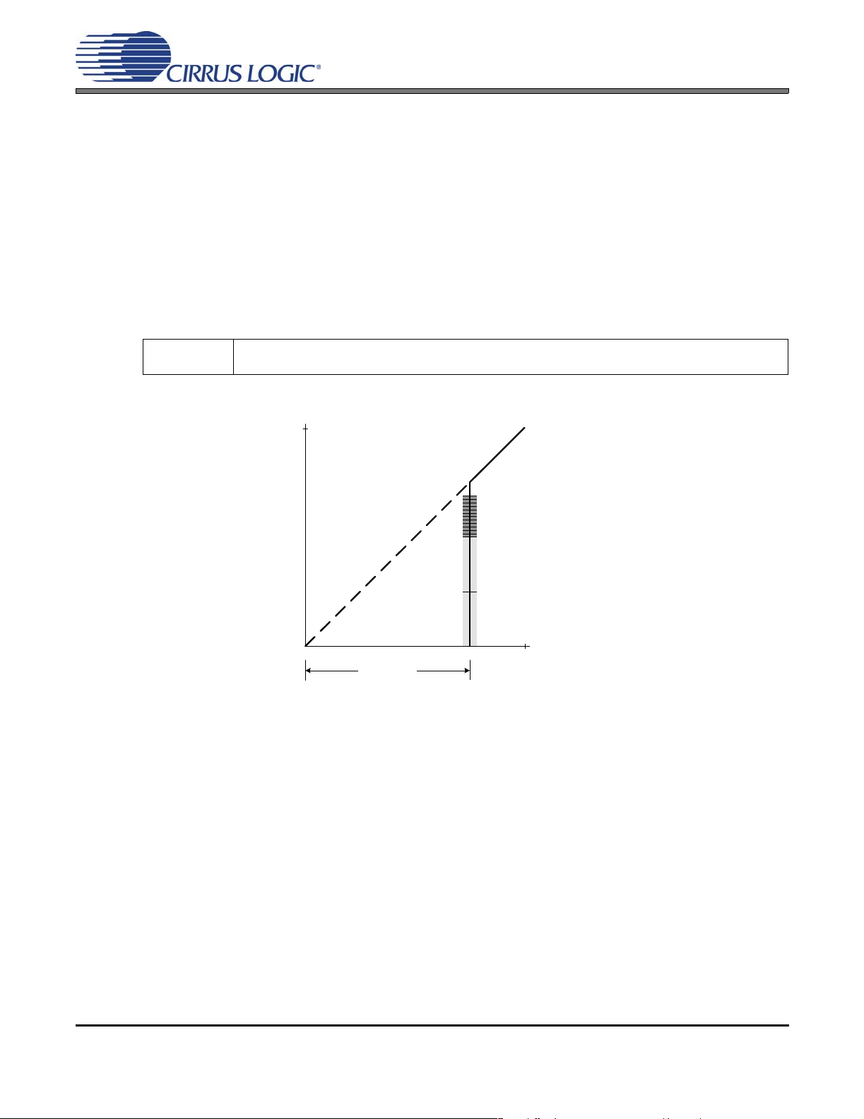
4.3.8 Noise Gate
The noise gate may be used to mute signal levels that fall below a programma ble threshold. This prevents
the ALC from applying gain to noise. A programmable delay may be used to set the minimum ti me before
the noise gate attacks the signal.
*Maximum noise gate attenuation levels will depend on the gain applied in either the PGA or MIC preamplifier. For example: If both +32 dB pre-amplification and +12 dB programmable gain is applied, the
maximum attenuation that the noise gate achieves will be 52 dB (-96 + 32 + 12) below full-scale.
Ramp down time to the maximum setting is affected by the SOFTx bit.
Recommended settings: For best results, enable soft ramp for the d igital attenuator. When the a nalog in-
puts are configured for differential signals (see “Differential Inputs” on page 29), en able the NG_ALL bit
to trigger the noise gate only when both inputs fall below the threshold.
Software
Controls:
CS42L51
“Noise Gate Configuration & Misc. (Address 1Fh)” on page 70, “ADC Control (Address 06h)” on
page 52.
Output
(dB)
1
=
N
E
G
N
0
=
N
E
G
N
Maximum Attenuation*
-96 -40
THRESH[2:0]
Figure 13. Noise Gate Attenuation
-52 dB
-64 dB
-80 dB
Input (dB)
32 DS679A2

4.4 Analog Outputs
AOUTA and AOUTB are the ground-centered line or headphone ou tputs. Various signal processin g options
are available, including digital mixes with the ADC signal and an internal Beep Generator. T he desired p ath
to the DAC must be selected using the DATA_SEL[1:0] bits.
Software
Controls:
INPUTS FROM ADCA
and ADCB
“DAC Control (Address 09h)” on page 55.
CS42L51
SIGNAL PROCESSING ENGINE (SPE)
MUTE_ADCMIXA
MUTE_ADCMIXB
ADCMIXA_VOL[6:0]
ADCMIXB_VOL[6:0]
+12dB/-51.5dB
0.5dB steps
VOL
OFFTIME[2:0]
ONTIME[3:0]
FREQ[3:0]
REPEAT
BEEP
VOL
PCMA[1:0]
PCMB[1:0]
ADCA[1:0]
ADCB[1:0]
Channel
Beep
Generator
Swap
BPVOL[4:0]
0dB/-50dB
2.0dB steps
MUTE_PCMMIXA
MUTE_PCMMIXB
PCMMIXA_VOL[6:0]
PCMMIXB_VOL[6:0]
DEEMPH
+12dB/-51.5dB
0.5dB steps
PCM Serial Interface
Demph
Digital Mix to ADC
Serial Interface
4.4.1 De-Emphasis Filter
The CODEC includes on-chip digital de-emphasis optimized for a sample rate of 44.1 kHz. The filter response is shown in Figure 15. The de-emphasis feature is included to accommodate audio recordings
that utilize 50/15 µs pre-emphasis equalization as a means of noise reduction. De-empha sis is only available in Single Speed Mode.
Software
Controls:
Hardware
Control:
“DAC Control (Address 09h)” on page 55.
Pin Setting Selection
“DEM” pin 4.
OUTA_VOL[7:0]
OUTB_VOL[7:0]
+12dB/-102dB
0.5dB steps
Chnl Vol.
Settings
Channel
VOL
Swap
Σ
Σ
DAC_SZC[1:0]
DACA_MUTE
DACB_MUTE
INV_DACA
INV_DACB
DAC_SNGVOL
AMUTE
VOL
TC_EN
Treble/
Control
BASS_CF[1:0]
TREB_CF[1:0]
+12.0dB/-10.5dB
Figure 14. Output Architecture
LO
HI
Bass/
BASS[3:0]
TREB[3:0]
1.5dB steps
ARATE[7:0]
RRATE[7:0]
MAX[2:0]
MIN[2:0]
LIM_SRDIS
LIM_ZCDIS
LIMIT_EN
Limiter
Peak
Detect
No De-Emphasis
De-Emphasis Applied
DATA_SEL[1:0]
10
01
00
PDN_DACA
PDN_DACB
Switched
Capacitor DAC
and Filter
Headphone
Amp - GND
Centered
Charge
CHRG_FREQ[3:0]
HP_GAIN[2:0]
Pump
Left/Right
HP Out
Gain
dB
T1=50 µs
0dB
T2 = 15 µs
-10dB
F1 F2
3.183 kHz 10.61 kHz
Frequency
Figure 15. De-Emphasis Curve
DS679A2 33

4.4.2 Volume Controls
Three digital volume control functions are implemented, offering independent control over the ADC and
PCM signal paths into the mixer as well as a combined control over the mixed signals. All volume controls
are programmable to ramp in increments of 0.125 dB at a rate controlled by the DAC soft ramp/zero cross
settings.
All signal paths may also be independently muted via mute control bits. When enabled, each bit attenuates the signal to its maximum value. When the mute bit is disabled, the signal returns to the attenuation
level set in the respective volume control regis ter. The attenuation is ramped up and down at the rate
specified by the DAC_SZC[1:0] bits.
Software
Controls:
“ADCx Mixer Volume Control: ADCA (Address 0Eh) & ADCB (Address 0Fh)” on page 58 , “PCMX
Mixer Volume Control: PCMA (Address 10h) & PCMB (Address 11h)” on page 59, “AOUTx Volume Control: AOUTA (Address 16h) & AOUTB (Address 17h)” on page 64, “DAC Output Control
(Address 08h)” on page 54.
4.4.3 Mono Channel Mixer
A channel mixer may be used to create a mix of the left and right channels for either the PCM or ADC
signals. This mix allows the user to produce a MONO signal fr om a stereo source. Th e mixer may also be
used to implement a left/right channel swap.
Software
Controls:
“ADC & PCM Channel Mixer (Address 18h)” on page 64.
CS42L51
4.4.4 Beep Generator
The Beep Generator generates audio freq uencies across approximately two octave major scales. It offers
three modes of operation: Continuous, multiple and single (one-shot) beeps. Sixteen on and eight off
times are available.
NOTE: The Beep is generated before the limiter and may affect desired limiting performance. If the limiter
function is used, it may be required to set the Beep volume sufficiently below the threshold to prevent the
peak detect from triggering. Since the master volume control, AOUTx_VOL[7:0], will affect the Beep volume, DAC volume may alternatively be controlled using the PCMMIXx_VOL[6:0] bits.
Software
Controls:
BPVOL[4:0]
REPEAT = '1'
BEEP = '1'
REPEAT = '1'
BEEP = '0'
REPEAT = '0'
BEEP = '1'
“Beep Frequency & Timing Configuration (Address 12h)” on page 60, “Beep Off Time & Volume
(Address 13h)” on page 61, “Beep Configuration & Tone Configuration (Address 14h)” on page 62
CONTINUOUS BEEP: Beep turns on at a configurable frequency (FREQ) and volume (BPVOL) and remains
on until REPEAT is cleared.
MULTI-BEEP: Beep turns on at a configurable frequency (FREQ)
and volume (BPVOL) for the duration of ONTIME and turns off for
the duration of OFFTIME. On and off cycles are repeated until
REPEAT is cleared.
SINGLE-BEEP: Beep turns on at a
configurable frequency (FREQ) and
volume (BPVOL) for the duration of
ONTIME. BEEP must be cleared
and set for additional beeps.
...
FREQ[3:0]
ONTIME[3:0] OFFTIME[2:0]
Figure 16. Beep Configuration Options
34 DS679A2

4.4.5 Tone Control
Shelving filters are used to implement bass and treble (boost and cut) with four selectable corner frequencies. Boosting will affect peak detect and limiting when levels exceed the maximum threshold settings.
Software
Controls:
4.4.6 Limiter
When enabled, the limiter monitors the digital input signal before the DAC m odulator, detects when levels
exceed the maximum threshold settings and lowers the AOUT volume at a programmable attack rate below the maximum threshold. When the input signal level falls below the maximum threshold, the AOUT
volume returns to its original level set in the Volume Control register at a programmable release rate . Attack and release rates are affected by the DAC soft ramp/zero cross settings and sample rate, Fs. Limiter
soft ramp and zero cross dependency may be independently enabled/disabled.
Recommended settings: Best limiting performance may be realized with the fastest attack and slowest
release setting with soft ramp enabled in the control registers. The “cushion” bits allow the user to set a
threshold slightly below the maximum threshold for hysteresis control - this cushions the sound as th e limiter attacks and releases.
trolled and should not be adjusted manually. Alternative volume control may be realized using the
PCMMIXx_VOL[6:0] bits.
Software
Controls:
CS42L51
“Tone Control (Address 15h)” on page 63.
NOTE: When the Limiter is enabled the AOUT Volume is automatically con-
“Limiter Release Rate Register (Address 1Ah)” on page 66, “Limiter Attack Rate Register (Address
1Bh)” on page 67, “DAC Control (Address 09h)” on page 55
Input
MAX[2:0]
Limiter
Output
(after Limiter)
MAX[2:0]
Volume
ATTACK/RELEASE SOUND
CUSHION
AOUTx_VOL[7:0] volume
control should NOT be
adjusted manually when
Limiter is enabled.
CUSH[2:0]
RRATE[5:0]ARATE[5:0]
Figure 17. Peak Detect & Limiter
DS679A2 35

4.4.7 Line-Level Outputs and Filtering
The CODEC contains on-chip buffer amplifiers capable of producing line level single-ended outputs on
AOUTA and AOUTB. These amplifiers are ground centered and do not have any DC offset. A load stabilizer circuit, shown in the “Typical Connection Diagram (Software Mode)” on page 10 and the “Typical
Connection Diagram (Hardware Mod e)” on page 11, is required on the analog outputs. This allows the
DAC amplifiers to drive line or headphone outputs.
Also shown in the Typical Connection diagrams is the recommended passive output filter to support high-
er impedances such as those found on the inputs to operational amplifiers. “Rext”, shown in the typical
connection diagrams, is the input impedance of the receiving device.
The invert and digital gain controls may be used to provide phase and/o r amplitude compensation for an
external filter.
The delta-sigma conversion process produces high frequency noise beyond the audio pa ssband, most of
which is removed by the on-chip analog filters. The re maining ou t-of-band noise can be attenua ted using
an off-chip low pass filter.
Software
Controls:
“DAC Output Control (Address 08h)” on page 54, “AOUTx Volume Control: AOUTA (Address 16h)
& AOUTB (Address 17h)” on page 64.
4.4.8 On-Chip Charge Pump
An on-chip charge pump derives a negative supply voltage from the VA_HP supply. This provides dual
rail supplies allowing a full-scale output swing centered around ground and eliminates the need for large,
DC-blocking capacitors. Added benefits include greater pop suppression and improved low frequency
(bass) response.
drop on the VA_HP supply will directly impact the derived negative voltage on the charge pump supply,
VSS_HP, and may result in clipping.
Note: Series resistance in the path of the power supplies must be avoided. Any voltage
CS42L51
The FLYN and FLYP pins connect to internal switches that char ges and discharges the externa l capacitor
attached, at a default switching frequency. This frequency may be adjusted in the control port registers.
Increasing the charge-pumping capacitor will slightly decease the pumping frequency. The capacitor connected to VSS_HP acts as a charge reservoir for the negative supply as well as a filter for the ripple induced by the charge pump. Increasing this capacitor will decrease the ripple on VSS_HP. Refer to the
typical connection diagrams in Figure 1 on page 10 or Figure 2 on page 11 for the recommended capacitor
values for the charge pump circuitry.
Software
Controls:
“Charge Pump Frequency (Address 21h)” on page 71.
36 DS679A2

4.5 Serial Port Clocking
The CODEC serial audio interface port operates either as a slave or master. It accepts externally generated
clocks in slave mode and will generate synchronous clocks derived from an input master clock (MCLK) in
master mode.
The frequency of the MCLK must be an integer m ultiple of, and synchro nous with, the system sample rate,
Fs. The LRCK frequency is equal to Fs, the frequency at which audio samples for each channel are clocke d
into or out of the device.
CS42L51
The SPEED and MCLKDIV2 software control bits or the SDOUT/(M/S
pins, configure the device to generate the proper clocks in Master Mode and receive the proper clocks in
Slave Mode. The value on the SDOUT pin is latched immediately after powering up in hardware mode.
Software
Control:
Hardware
Control:
4.5.1 Slave
LRCK and SCLK are inputs in Slave Mode. The speed of the CODEC is automatically determined based
on the input MCLK/LRCK ratio when the Auto-Detect function is enabled. Certain input clock ratios will
then require an internal divide-by-two of MCLK* using either the MCLKDIV2 bit or the MCLKDIV2 standalone control pin.
Additional clock ratios are allowed when the Auto-Detect function is disabled; but the appropriate speed
mode must be selected using the SPEED[1:0] bits.
Auto-Detect QSM HSM SSM DSM
Disabled
(Software
Mode only)
Enabled 1024, 1536, 2048*,
*MCLKDIV2 must be enabled.
) and MCLKDIV2 stand-alone control
“MIC Power Control & Speed Control (Address 03h)” on page 48, “DAC Control (Address 09h)” on
page 55.
Pin Setting Selection
“SDOUT, M/S” pin 2947 kΩ Pull-down Slave
47 kΩ Pull-up Master
“MCLKDIV2” pin 2 LO No Divide
HI MCLK is divided by 2 prior to all internal circuitry.
512, 768, 1024,
1536, 2048, 3072
3072*
256, 384, 512, 768,
1024, 1536
512, 768, 1024*,
1536*
Table 3. MCLK/LRCK Ratios
128, 192, 256, 384,
256, 384, 512*, 768* 128, 192, 256*, 384*
128, 192, 256, 384
512, 768
DS679A2 37

4.5.2 Master
LRCK and SCLK are internally derived from the internal MCLK (after the divide, if MCLKDIV2 is enabled).
In hardware mode the CODEC operates in single-speed only. In software mode the CODEC operates in
either quarter-, half-, single- or double-speed depending on the setting of the SPEED[1:0] bits.
CS42L51
÷ 1
0
MCLK
÷ 2
1
MCLKDIV2
Figure 18. Master Mode Timing
4.5.3 High-Impedance Digital Output
The serial port may be placed on a clock/data bus that allows multiple masters, without the need for external buffers. The 3ST_SP bit places the internal buffers for the serial port signals in a high-impedance
state, allowing another device to transmit clocks or data without bus contention.
÷ 128
÷ 128
÷ 256
÷ 512
÷ 2
÷ 2
÷ 4
÷ 8
Double
Speed
Single
Speed
Half
Speed
Quarter
Speed
Double
Speed
Single
Speed
Half
Speed
Quarter
Speed
00
01
10
11
SPEED[1:0]
00
01
10
11
LRCK Output
(Equal to Fs)
SCLK Output
CS42L51
Transmitting Device #1
3ST_SP
Transmitting Device #2
SDOUT
SCLK/LRCK
Receiving Device
Figure 19. Tri-State Serial Port
38 DS679A2
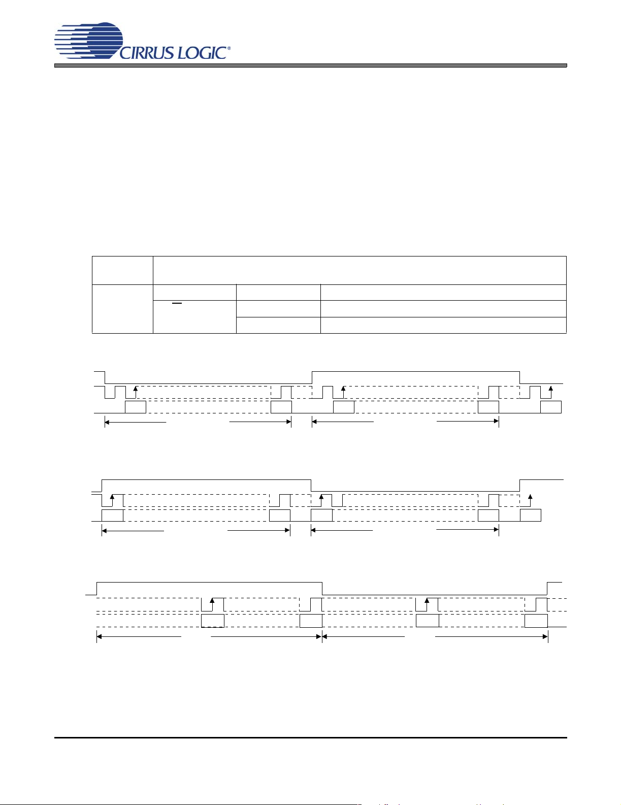
4.5.4 Quarter- and Half-Sp eed Mode
Quarter-Speed Mode (QSM) and Half-Speed Mode (HSM) allow lower sample rates while maintaining a
relatively flat noise floor in the typical audio band of 20 Hz - 20 kHz. Single-Speed Mode (SSM) wi ll allow
lower frequency sample rates; however, the DAC's noise floor, that normally rises out-of-band, will scale
with the lower sample rate and begin to rise within th e audio band. QSM and HSM corre cts for most of
this scaling, effectively increasing the dynamic range of the CODEC at lower sample rates, relative to
SSM.
4.6 Digital Interface Formats
The serial port operates in standard I²S, Left-Justified or Right-Justified(DAC only) digital interface formats
with varying bit depths fr om 16 to 24. Data is clocked out of the ADC or in to t he DA C o n th e rising edge of
SCLK. Figures 20-22 illustrate the general structure of each format. Refer to “Switching Specifications - Se-
rial Port” on page 20 for exact timing relationship between clocks and data.
CS42L51
SDOUT
LRCK
SCLK
SDIN
SDOUT
LRCK
SCLK
SDIN
Software
Control:
Hardware
Control:
“Interface Control (Address 04h)” on page 49.
Pin Setting Selection
“I²S/LJ” pin 3 LO Left-Justified Interface
HI I²S Interface
Left C hannel Right C hannel
MSB LSB
AOUTA / AINxA
Figure 20. I²S Format
Left Channel Right Channel
MSB LSB
AOUTA / AINxA
Figure 21. Left-Justified Format
MSB
MSB
AOUTB / AINxB
AOUTB / AINxB
LSB
LSB
MSB
MSB
LRCK
SCLK
SDIN
Left Channel Right Channel
MSB LSB
AOUTA
MSB
AOUTB
LSB
Figure 22. Right-Justified Format (DAC only)
DS679A2 39

4.7 Initialization
The initialization and Power-Down sequence flow chart is shown in Figure 23 on page 41. The CODEC e nters a Power-Down state upon initial power-up. The interpolation & decimation filters, delta-sigma modulators and control port registers are reset. The internal voltage reference, multi-bit DAC and ADC and
switched-capacitor low-pass filters are powered down.
CS42L51
The device will remain in the Power-Down state until the RESET
cessible once RESET
in “Software Mode” on page 42. If a valid write sequence to the control port is not made within approximately
10 ms, the CODEC will enter Hardware Mode.
Once MCLK is valid, the quiescent voltage, VQ, and the internal voltage references, DAC_FILT+ and
ADC_FILT+, will begin powering up to normal operation. The charge pump slowly powers up and charges
the capacitors. Power is then applied to the headphone amplifiers and switched-capacitor filters, and the analog/digital outputs enter a muted state. Once LRCK is valid, MCLK occurrences are counted over one LRCK
period to determine the MCLK/LRCK frequency ratio and normal operation begins.
is high and the desired register settings can be loaded per the interface descriptions
4.8 Recommended Power-Up Sequence
1. Hold RESET low until the power supplies are stable.
2. Bring RESET
3. For Software Mode operation, set the PDN bit to ‘1’b in under 10 ms. This will place the device in “standby”.
4. Load the desired register settings while keeping the PDN bit set to ‘1’b.
5. Start MCLK to the appropriate freque n cy, as discu sse d in Sec tio n 4. 5.
6. Set the PDN bit to ‘0’b.
7. Apply LRCK, SCLK and SDIN for normal operation to begin.
8. Bring RESET
prevent power glitch related issues.
high. After approximately 10 ms, the device will enter Hardware Mode.
low if the analog or digital supplies drop below the recommended operating condition to
pin is brought high. The control port is ac-
40 DS679A2
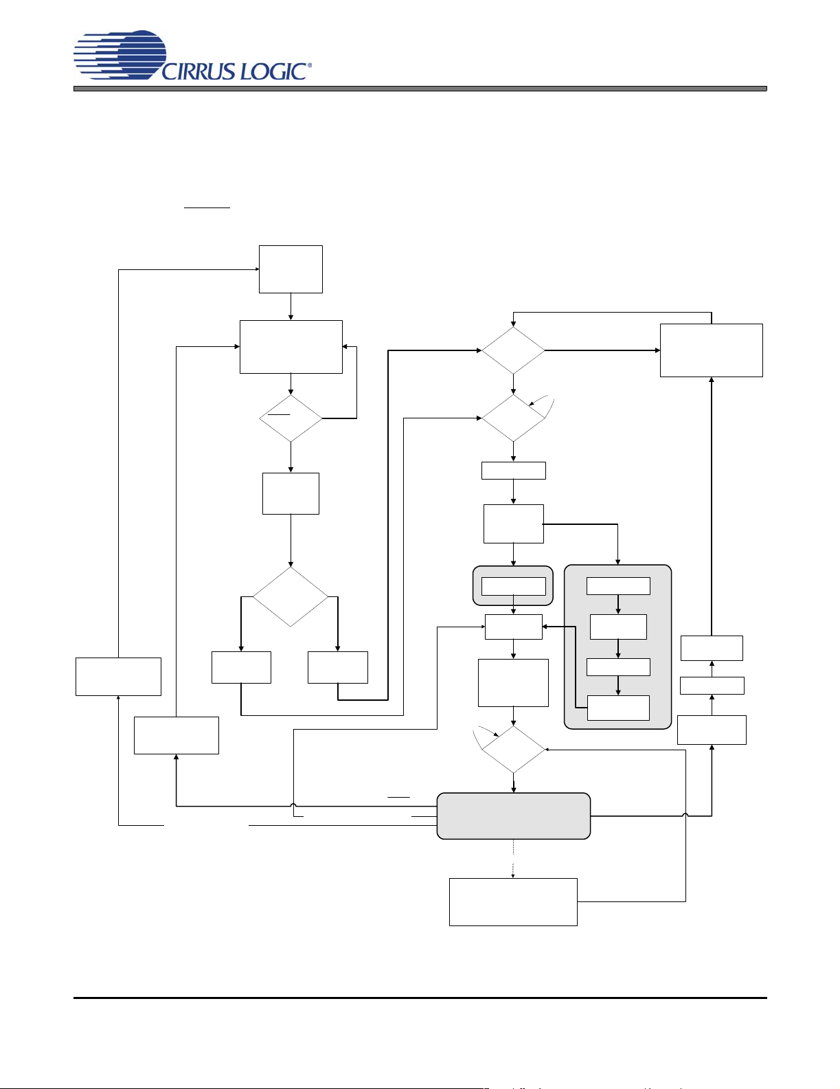
4.9 Recommended Power-Down Sequence
To minimize audible pops when turning off or placing the CODEC in standby,
1. Mute the DAC’s & ADC’s.
2. Set the PDN bit in the power control register to ‘1’b. The CODEC will not power down until it reaches a
fully muted sate.
3. Bring RESET
low.
No Power
1. No audio signal
generated.
CS42L51
Power Off Transition
1. Audible pops.
Reset Transition
1. Pops suppressed.
Off Mode (Power Applied)
1. No audio signal generated.
2. Control Port Registers reset
to default.
RESET = Low?
Control Port
Control Port Valid
No
Write Seq. within
Hardware Mode
Minimal feature
set support.
No
Active
10 ms?
Yes
Yes
Software Mode
Registers setup to
desired settings.
PDN bit = '1'b?
Valid
MCLK Applied?
20 ms delay
Charge Caps
1. VQ Charged to
quiescent voltage.
2. Filtx+ Charged.
ADC Initialization
2048 internal
MCLK cycle delay
Digital/Analog
Output Muted
Sub-Clocks Applied
1. LRCK valid.
2. SCLK valid.
3. Audio samples
processed.
No
Valid
MCLK/LRCK
Ratio?
Yes
Standby Mode
Yes
No
No
DAC Initialization
50 ms delay
Charge Pump
Powered Up
20 µs delay
Headphone Amp
Powered Up
1. No audio signal generated.
2. Control Port Registers retain
settings.
Headphone Amp
Powered Down
20 µs delay (DAC
only)
Stand-By
Transition
1. Pops suppressed.
ERROR: Power removed
RESET = Low
ERROR: MCLK/LRCK ratio change
Audio signal generated per control port or stand-
Normal Operation
alone settings.
ERROR: MCLK removed
Analog Output Freeze
1. Aout bias = last audio sample.
2. DAC Modulators stop operation.
3. Audible pops.
PDN bit set to '1'b
(software mode only)
Figure 23. Initialization Flow Chart
DS679A2 41

4.10 Software Mode
The control port is used to access the registers allowing the CODEC to be configure d for the desired operational modes and formats. The operation of the control port ma y be completely asynchron ous with respect
to the audio sample rates. However, to avoid potential interference problems, the control port pins should
remain static if no operation is required.
The control port operates in 2 modes: SPI and I²C, with the CODEC acting as a slave device. SPI mode is
selected if there is a high-to-low transition on the AD0/CS
I²C mode is selected by connecting the AD0/CS
selecting the desired AD0 bit address state.
4.10.1 SPI Control
In SPI mode, CS is the CS42L51 chip select signal, CCLK is the control port bit clock (input into the
CS42L51 from the microcontroller), CDIN is the input data line from the microcontroller. Data is clocked
in on the rising edge of CCLK. The CODEC will only support write operations. Read request will be ignored.
CS42L51
pin after the RESET pin has been brought high.
pin through a resistor to VL or DGND, thereby permanently
Figure 24 shows the operation of the control port in SPI mode. To write to a register, bring CS
first seven bits on CDIN form the chip address and must be 1001010. The eighth bit is a read/write indicator (R/W
), which should be low to write. The next eight bits form the Memory Address Pointer (MAP),
which is set to the address of the register that is to be updated. Th e next eight bits are the data wh ich will
be placed into the register designated by the MAP.
There is MAP auto increment capability, enabled by the INCR bit in the MAP register. If INCR is a zero,
the MAP will stay constant for successive read or writes. If INCR is set to a 1, the MAP will autoincrement
after each byte is read or written, allowing block reads or writes of successive registers.
CS
CCLK
CDIN
4.10.2 I²C Control
In I²C mode, SDA is a bidirectional data line. Data is clocked into and out of the part by the clock, SCL.
There is no CS
through a resistor to VL or DGND as desired. The state of the pin is sensed while the
reset.
low. The
0 1 2 3 8 9 12 16 1710 11 13 14 15
CHIP ADDRESS (WRITE) MAP BYTE DATA
1 0 0 1 0 1 0 0
4 5 6 7
INCR 6 5 4 3 2 1 0 7 6 1 0
Figure 24. Control Port Timing in SPI Mode
DATA +n
7 6 1 0
pin. Pin AD0 forms the least significant bit of the chip address and should be connected
CS42L51 is being
The signal timings for a read and write cycle are shown in Figure 25 and Figure 26. A Start c ondition is
defined as a falling transition of SDA while the clock is high. A Stop condition is a rising transition while
the clock is high. All other transitions of SDA occur while the clock is low. The first byte sent to the
CS42L51
after a Start condition consists of a 7 bit chip address field a nd a R/W bit (high for a read, low for a write).
The upper 6 bits of the 7-bit address field are fixed at 100101. To communicate with a
address field, which is the first byte sent to the
the AD0 pin. The eighth bit of the address is the R/W
CS42L51, should match 100101 followed by the setting of
bit. If the operation is a write, the next byte is the
CS42L51, the chip
Memory Address Pointer (MAP) which selects the register to be read or written. If the o peration is a read,
42 DS679A2
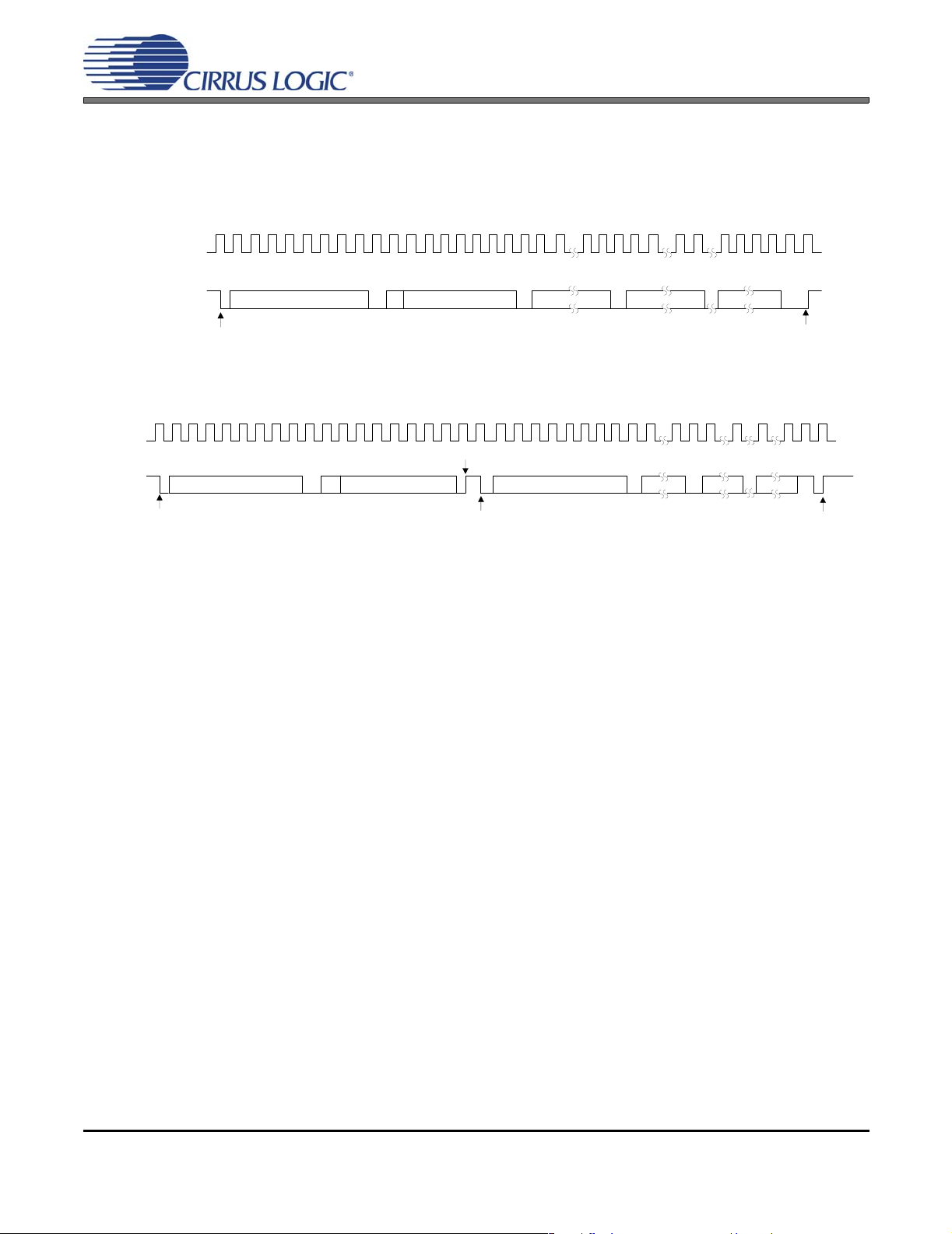
CS42L51
the contents of the register pointed to by the MAP will be output. Setting the auto increment bit in MAP
allows successive reads or writes of consecutive registers. Each byte is separated by an acknowledge
bit. The ACK bit is output from the
the microcontroller after each transmitted byte.
CS42L51 after each input byte is read, and is input to the CS42L51 from
SCL
SDA
26
DATA +1
DATA +n
ACKACKACK
STOP
SCL
SDA
0 1 2 3 8 9 12 16 17 18 1910 11 13 14 15 27 28
CHIP ADDRESS (WRITE) MAP BYTE DATA
1 0 0 1 0 1 AD0 0
START
4 5 6 7 24 25
INCR 6 5 4 3 2 1 0 7 6 1 0 7 6 1 0 7 6 1 0
ACK
Figure 25. Control Port Timing, I²C Write
2 3 10 11 17 18 19 25
CHIP ADDRESS (WRITE)
1 0 0 1 0 1 AD0 0
START
MAP BYTE
INCR 6 5 4 3 2 1 0
ACK
168 9 12 13 14 154 5 6 7 0 1 20 21 22 23 24
STOP
ACK
START
CHIP ADDRESS (READ)
1 0 0 1 0 1 AD0 1
26 27 28
DATA
7 0 7 0 7 0
ACK
DATA +1
ACK
DATA + n
NO
ACK
STOP
Figure 26. Control Port Timing, I²C Read
Since the read operation can not set the MAP, an aborted write operation is used as a preamble. As
shown in Figure 26, the write operation is aborted after the acknowledge for the MAP byte by sending a
stop condition. The following pseudocode illustrates an aborted write operation followed by a read operation.
Send start condition.
Send 100101x0 (chip address & write operation).
Receive acknowledge bit.
Send MAP byte, auto increment off.
Receive acknowledge bit.
Send stop condition, aborting write.
Send start condition.
Send 100101x1(chip address & read operation).
Receive acknowledge bit.
Receive byte, contents of selected register.
Send acknowledge bit.
Send stop condition.
Setting the auto increment bit in the MAP allows successive reads or writes of consecutive registers. Each
byte is separated by an acknowledge bit.
DS679A2 43

4.10.3 Memory Address Pointer (MAP)
The MAP byte comes after the address byte and selects the register to be read or written. Refer to the
pseudo code above for implementation details.
4.10.3.1 Map Increment (INCR)
The device has MAP auto increment capability enabled by the INCR bit (the MSB) of the MAP. If INCR is
set to 0, MAP will stay constant for successive I²C writes or reads and SPI writes. If INCR is set to 1, MAP
will auto increment after each byte is written, allowing block reads or writes of successive registers.
CS42L51
44 DS679A2

CS42L51
5. REGISTER QUICK REFERENCE
Software Mode register defaults are as shown. “Reserved” registers must maintain their default state.
AddrFunction76543210
01h ID. Chip_ID4 Chip_ID3 Chip_ID2 Chip_ID1 Chip_ID0 Rev_ID2 Rev_ID1 Rev_ID0
p47. default11011000
02h Power Ctl. 1. Reserved PDN_DACB PDN_DACA PDN_PGAB PDN_PGAA PDN_ADCB PDN_ADCA PDN
p47. default00000000
03h Speed Ctl. &
Power Ctl. 2.
p48. default10101110
04h Interface Ctl. SDOUT->SDIN M/S
p49. default00000000
05h MIC Control
& Misc.
p51. default00000000
06h ADC Control. ADCB_HPFENADCB_HP
p52. default10100000
07h ADC Input
Select. ,
Invert, Mute.
p53. default00000000
08h DAC Output
Control.
p54. default01100000
09h DAC Control. DATA_SEL1 DATA_SEL0 FREEZE Reserved DEEMPH Reserved DAC_SZC1 DAC_SZC0
p55. default00000110
0Ah ALCA SZC &
PGAA Volume.
p56. default00000000
0Bh ALCB SZC &
PGAB Volume .
p56. default00000000
0Ch ADCA Atten-
uator.
p57. default00000000
0Dh ADCB Atten-
uator .
p57. default00000000
0Eh Vol. Control
ADCMIXA.
p58. default10000000
0Fh Vol. Control
ADCMIXB.
p58. default10000000
10h Vol. Control
PCMMIXA.
p59. default10000000
11h Vol. Control
PCMMIXB.
p59. default10000000
AUTO SPEED1 SPEED0 3-ST_SP PDN_MICB PDN_MICA PDN_
DAC_DIF2 DAC_DIF1 DAC_DIF0 ADC_I²S/LJ DIGMIX MICMIX
ADC_SNGVOL ADCB_
DBOOST
FRZ
AINB_MUX1 AINB_MUX0AINA_MUX1 AINA_MUX0 INV_ADCB INV_ADCA ADCB_
HP_GAIN2 HP_GAIN1 HP_GAIN0 DAC_SNG
ALCA_SR
DIS
ALCB_SR
DIS
ADCA_ATT7 ADCA_ATT6ADCA_ATT5 ADCA_ATT4 ADCA_ATT3 ADCA_ATT2 ADCA_ATT1 ADCA_ATT0
ADCB_ATT7 ADCB_ATT6ADCB_ATT5 ADCB_ATT4 ADCB_ATT3 ADCB_ATT2 ADCB_ATT1 ADCB_ATT0
MUTE_ADC
MIXA
MUTE_ADC
MIXB
MUTE_PCM
MIXA
MUTE_PCM
MIXB
ALCA_ZC
DIS
ALCB_ZC
DIS
ADCMIXA
VOL6
ADCMIXB
VOL6
PCMMIXA
VOL6
PCMMIXB
VOL6
ADCA_
DBOOST
ADCA_HPFENADCA_HP
Reserved PGAA
Reserved PGAB
ADCMIXA
VOL5
ADCMIXB
VOL5
PCMMIXA
VOL5
PCMMIXB
VOL5
MICBIAS_
SEL
FRZ
VOL
VOL4
VOL4
ADCMIXA
VOL4
ADCMIXB
VOL4
PCMMIXA
VOL4
PCMMIXB
VOL4
MICBIAS_
LVL1
SOFTB ZCROSSB SOFTA ZCROSSA
INV_DACB INV_DACA DACB_
PGAA
VOL3
PGAB
VOL3
ADCMIXA
VOL3
ADCMIXB
VOL3
PCMMIXA
VOL3
PCMMIXB
VOL3
MICBIAS_
LVL0
PGAA
VOL2
PGAB
VOL2
ADCMIXA
VOL2
ADCMIXB
VOL2
PCMMIXA
VOL2
PCMMIXB
VOL2
MICBIAS
MICB_
BOOST
MUTE
MUTE
PGAA
VOL1
PGAB
VOL1
ADCMIXA
VOL1
ADCMIXB
VOL1
PCMMIXA
VOL1
PCMMIXB
VOL1
MCLKDIV2
MICA_
BOOST
ADCA_
MUTE
DACA_
MUTE
PGAA
VOL0
PGAB
VOL0
ADCMIXA
VOL0
ADCMIXB
VOL0
PCMMIXA
VOL0
PCMMIXB
VOL0
DS679A2 45
CS42L51
AddrFunction76543210
12h BEEP Freq. &
OnTime .
p60. default 0 0 0 0 0 0 0 0
13h BEEP Off
Time & Vol.
p61. default 0 0 0 0 0 0 0 0
14h BEEP Con-
trol & Tone
Config.
p62. default 0 0 0 0 0 0 0 0
15h Tone Control. TREB3 TREB2 TREB1 TREB0 BASS3 BASS2 BASS1 BASS0
p63. default 1 0 0 0 1 0 0 0
16h Vol. Control
AOUTA.
p64. default 0 0 0 0 0 0 0 0
17h Vol. Control
AOUTB.
p64. default 0 0 0 0 0 0 0 0
18h PCM & ADC
Channel
Mixer.
p64. default 0 0 0 0 0 0 0 0
19h Limiter
Threshold &
SZC Disable.
p65. default 0 0 0 0 0 0 0 0
1Ah Limiter Con-
fig & Release
Rate.
p66. default 0 1 0 0 0 0 0 0
1Bh Limiter Attack
Rate.
p67. default 0 0 0 0 0 0 0 0
1Ch ALC Enable
& Attack
Rate.
p67. default 0 0 0 0 0 0 0 0
1Dh ALC Release
Rate.
p68. default 0 0 0 0 0 0 0 0
1Eh ALC Thresh-
old.
p69. default 0 0 0 0 0 0 0 0
1Fh Noise Gate
Config.
p70. default 0 0 0 0 0 0 0 0
20h Status. Reserved SP_CLKERRSPEB_OVFL SPEA_OVFL PCMA_OVFL PCMB_OVFL ADCA_OVFL ADCB_OVFL
FREQ3 FREQ2 FREQ1 FREQ0 ONTIME3 ONTIME2 ONTIME1 ONTIME0
OFFTIME2 OFFTIME1 OFFTIME0 BPVOL4 BPVOL3 BPVOL2 BPVOL1 BPVOL0
REPEAT BEEP Reserved TREB_CF1 TREB_CF0 BASS_CF1 BASS_CF0 TC_EN
AOUTA_
VOL7
AOUTB_
VOL7
PCMA1 PCMA0 PCMB1 PCMB0 ADCA1 ADCA0 ADCB1 ADCB0
MAX2 MAX1 MAX0 CUSH2 CUSH1 CUSH0 LIM_SRDIS LIM_ZCDIS
LIMIT_EN LIMIT_ALL LIM_RRATE5LIM_RRATE4LIM_RRATE3LIM_RRATE2LIM_RRATE1LIM_RRATE
Reserved Reserved LIM_ARATE5 LIM_ARATE4 LIM_ARATE3 LIM_ARATE2 LIM_ARATE1 LIM_ARATE0
ALC_ENB ALC_ENA ALC_ARATE5AALC_RATE4ALC_ARATE
Reserved Reserved ALC_RRATE5ALC_RRATE4ALC_RRATE3ALC_RRATE2ALC_RRATE1ALC_RRATE
MAX2 MAX1 MAX0 MIN2 MIN1 MIN0 Reserved Reserved
NG_ALL NG_EN NG_BOOST THRESH2 THRESH1 THRESH0 NGDELAY1 NGDELAY0
AOUTA_
VOL6
AOUTB_
VOL6
AOUTA_
VOL5
AOUTB_
VOL5
AOUTA_
VOL4
AOUTB_
VOL4
AOUTA_
VOL3
AOUTB_
VOL3
3
AOUTA_
VOL2
AOUTB_
VOL2
ALC_ARATE2ALC_ARATE1ALC_ARATE
AOUTA_
VOL1
AOUTB_
VOL1
AOUTA_
VOL0
AOUTB_
VOL0
0
0
0
p71. default 0 0 0 0 0 0 0 0
21h Charge Pump
Frequency.
p71. default 0 1 0 1 0 0 0 0
CHRG_FREQ3 CHRG_
FREQ2
CHRG_
FREQ1
CHRG_
FREQ0
Reserved Reserved Reserved Reserved
46 DS679A2

CS42L51
6. REGISTER DESCRIPTION
All registers are read/write except for the ch ip I.D. and Revision Register and In terrupt Status Register which are
read only. See the following bit definition tables for bit assignment information. The default state of each bit after a
power-up sequence or reset is listed in each bit description.
All “Reserved” registers must maintain their default state.
Note: Certain functions are only available when the “Signal Processing Engine to DAC” option is selected using
the DATA_SEL[1:0] bits, as described in section “DAC Data Selection (DATA_SEL[1:0])” on page 55.
6.1 Chip I.D. and Revision Register (Address 01h) (Read Only)
76543210
Chip_ID4 Chip_ID3 Chip_ID2 Chip_ID1 Chip_ID0 Rev_ID2 Rev_ID1 Rev_ID0
Chip I.D. (Chip_ID[4:0])
Default: 11011
Function:
I.D. code for the CS42L51. Permanently set to 11011.
Chip Revision (Rev_ID[2:0])
Default: 000
Function:
CS42L51 revision level. Revision A is coded as 000.
6.2 Power Control 1 (Address 02h)
76543210
Reserved PDN_DACB PDN_DACA PDN_PGAB PDN_PGAA PDN_ADCB PDN_ADCA PDN
Notes:
1. To activate the power down sequence for individual channels (A or B) both channels must first be powered down either by enabling the PDN bit or by enabling the power down bits for both channels. Enabling the power down bit on an individual channel basis after the CODEC has fully powered up, will
mute the selected channel without achieving any po we r sav ing s.
Recommended channel power down sequence: (1) Enable the PDN bit, (2) enable power down for the select channels, (2) disable the PDN bit.
Power Down DAC X (PDN_DACX)
Default: 0
0 - Disable
1 - Enable
Function:
DAC channel x will either enter a power down or muted state when this bit is enabled. See Note 1 above.
DS679A2 47
CS42L51
Power Down PGA X (PDN_PGAX)
Default: 0
0 - Disable
1 - Enable
Function:
PGA channel x will either enter a power down or muted state when this bit is enabled. See note 1 on page
47.
This bit is used in conjunction with AINx_MUX bits to determine the analog input path to the ADC. Refer to
“ADCX Input Select Bits (AINX_MUX[1:0])” on page 53 for the required settings.
Power Down ADC X (PDN_ADCX)
Default: 0
0 - Disable
1 - Enable
Function:
ADC channel x will either enter a power down or muted state when this bit is enabled. See note 1 on page
47.
Power Down (PDN)
Default: 0
0 - Disable
1 - Enable
Function:
The entire CODEC will enter a low-power state when this function is enabled. The contents of the control
port registers are retained in this mode.
6.3 MIC Power Control & Speed Control (Address 03h)
76543210
AUTO SPEED1 SPEED0 3-ST_SP PDN_MICB PDN_MICA PDN_MICBIAS MCLKDIV2
Auto-Detect Speed Mode (AUTO)
Default: 1
0 - Disable
1 - Enable
Function:
Enables the auto-detect circuitry for detecting the speed mode of the CODEC when o perating a s a slave.
When AUTO is enabled, the MCLK/LRCK ratio must be implemented according to Table 3 on page 37. The
SPEED[1:0] bits are ignored when this bit is enabled. Speed is determined by the MCLK/LRCK ratio.
Speed Mode (SPEED[1:0])
Default: 01
11 - Quarter-Speed Mode (QSM) - 4 to 12.5 kHz sample rates
10 - Half-Speed Mode (HSM) - 12.5 to 25 kHz sample rates
01 - Single-Speed Mode (SSM) - 4 to 50 kHz sample rates
00 - Double-Speed Mode (DSM) - 50 to 100 kHz sample rates
Function:
Sets the appropriate speed mode for the CODEC in master or slave mod e. QSM is optimized for 8 kHz sample rate and HSM is optimized for 16 kHz sample rate. These bits are ignored when the AUTO bit is enabled
(see Auto-Detect Speed Mode (AUTO) above).
48 DS679A2

CS42L51
Tri-State Serial Port Interface (3ST_SP)
Default: 0
0 - Disable
1 - Enable
Function:
When enabled, and the device is configured as a master, then all Serial Port interface signals will be placed
in a high-impedance output state. If the serial port interface is configured as a slave, only the SDOUT pin
will be placed in a high-impedance state. The other signals will remain as inputs.
Power Down MIC X (PDN_MICX)
Default: 1
0 - Disable
1 - Enable
Function:
When enabled, the microphone pre-amplifier for channel x will be in a power down state.
Power Down MIC BIAS (PDN_MICBIAS)
Default: 1
0 - Disable
1 - Enable
Function:
When enabled, the microphone bias circuit will be in a power down state.
MCLK Divide By 2 (MCLKDIV2)
Default: 0
0 - Disabled
1 - Divide by 2
Function:
Divides the input MCLK by 2 prior to all internal circuitry. This bit is ignored when the AUTO bit is disabled
in slave mode.
6.4 Interface Control (Address 04h)
76543210
SDOUT->SDIN M/S
SDOUT to SDIN Loopback (SDOUT->SDIN)
Default: 0
0 - Disabled; SDOUT internally disconnected from SDIN
1 - Enabled; SDOUT internally connected to SDIN
Function:
Internally loops the signal on the SDOUT pin to SDIN.
Master/Slave Mode (M/S)
DAC_DIF2 DAC_DIF1 DAC_DIF0 ADC_I²S/LJ DIGMIX MICMIX
Default: 0
0 - Slave
1 - Master
Function:
Selects either master or slave operation for the serial port.
DS679A2 49
CS42L51
DAC Digital Interface Format (DAC_DIF[2:0])
Default = 000
DAC_DIF[2:0] Description Figure
000 Left Justified, up to 24-bit data 21 on page 39
001 I²S, up to 24-bit data 20 on page 39
010 Right Justified, 24-bit data 22 on page 39
011 Right Justified, 20-bit data 22 on page 39
100 Right Justified, 18-bit data 22 on page 39
101 Right Justified, 16-bit data 22 on page 39
110 Reserved 100 Reserved -
Function:
Selects the digital interface format used for the data in on SDIN. The required relationship between the
Left/Right clock, serial clock and serial data is defined by the Digital Interface Format and the options are
detailed in the section “Digital Interface Formats” on page 39.
ADC I²S or Left-Justified (ADC_I²S/LJ)
Default: 0
0 - Left-Justified
1 - I²S
Function:
Selects either the I²S or Left-Justified digital interface format for the data on SDOUT. The required relationship between the Left/Right clock, serial clock and serial data is defined by the Digital Interface Format and
the options are detailed in the section “Digital Interface Formats” on page 39.
Digital Mix (DIGMIX)
Default: 0
DIGMIX DATA_SEL[1:0] Mix Selected
0 xx No Mix: ADC to ADC serial port, SDOUT data.
00 No Mix: SDIN data to ADC serial port, SDOUT data.
1
Function:
Selects between the ADC or a digital mix of the ADC and DAC into the serial port to the SDOUT pin. This
mix function is affected by the data select bits DATA_SEL[1:0].
Microphone Mix (MICMIX)
Default: 0
0 - Disabled; No Mix: Left/Right Channel to ADC serial port, SDOUT.
1 - Enabled; Mix: Differential mix ((A-B)/2)to ADC serial port, SDOUT.
01 Mix: ADC + SDIN data to ADC serial port, SDOUT data.
10 No Mix: ADC to ADC serial port, SDOUT data.
11 Reserved
Function:
Selects between the ADC stereo mix or a differential mix of analog inputs A and B.
50 DS679A2

CS42L51
6.5 MIC Control (Address 05h)
76543210
ADC_SNGVOL ADCB_DBOOST ADCA_DBOOST MICBIAS_SEL MICBIAS_LVL1 MICBIAS_LVL0 MICB_BOOST MICA_BOOST
ADC Single Volume Control (ADC_SNGVOL)
Default: 0
0 - Disabled
1 - Enabled
Function:
The individual PGA Volume (PGAx_VOLx) and ADC channel attenuation ( ADCx_ATTx) levels are independently controlled by their respective control registe rs when this function is disabled. Whe n enabled, the volume on both channels is determined by the ADCA Attenuator Control reg ister, or the PGAA Control register,
and the ADCB Attenuator and PGAB Control registers are ignored.
ADCx 20dB Digital Boost (ADCx_DBOOST)
Default: 0
0 - Disabled
1 - Enabled
Function:
Applies a 20dB digital gain to the input signal on ADC channel x, regardless of the input path.
MIC Bias Select (MICBIAS_SEL)
Default: 0
0 - MICBIAS on AIN3B/MICIN2 pin
1 - MICBIAS on AIN2B pin
Function:
Determines the output pin for the internally generated MICBIAS signal. If set to ‘0’b, then the MICBIAS is
output on the AIN3B/MICIN2 pin. If set to ‘1’b, then the MICBIAS is output on the AIN2B pin.
MIC Bias Level (MICBIAS_LVL[1:0])
Default: 00
00 - 0.8 x VA
01 - 0.7 x VA
10 - 0.6 x VA
11 - 0.5 x VA
Function:
Determines the output voltage level of the MICBIAS output.
MIC X Preamplifier Boost (MICX_BOOST)
Default: 0
0 - +16 dB Gain
1 - +32 dB Gain
Function:
Determines the amount of gain applied to the microphone preamplifier for channel x.
DS679A2 51

CS42L51
6.6 ADC Control (Address 06h)
76543210
ADCB_HPFEN ADCB_HPFRZ ADCA_HPFEN ADCA_HPFRZ SOFTB ZCROSSB SOFTA ZCROSSA
ADCX High-Pass Filter Enable (ADCX_HPFEN)
Default: 1
0 - High-pass filter is disabled
1 - High-pass filter is enabled
Function:
When this bit is set, the internal high-pass filter will be enabled for ADCx. When set to ‘0’, the high-pass filter
will be disabled. For DC measurements, this bit must be cleared to ‘0’. See “ADC Digital Filter Characteristics” on page 15.
ADCX High-Pass Filter Freeze (ADCX_HPFRZ)
Default: 0
0 - Continuous DC Subtraction
1 - Frozen DC Subtraction
Function:
The high-pass filter works by co ntinuously subtracting a meas ure of the DC offset from the ou tput of the
decimation filter. If the ADCx_HPFRZ bit is taken high during nor mal operation, the curren t value of the DC
offset is frozen and this DC offset will continue to be subtracted from the conversion result. For DC measurements, this bit must be set to ‘1’. See “ADC Digital Filter Characteristics” on page 15.
Soft Ramp CHX Control (SOFTX)
Default: 0
0 - Disabled
1 - Enabled
Function:
Soft Ramp allows level changes to be implemented via an incremental ramp. ADCx_ATT[7:0] digital attenuation changes are ramped from the current level to the new level at a rate of 0.125 dB per LRCK period.
PGAx_VOL[4:0] gain changes are ramped in 0.5 dB steps every 16 LRCK periods.
Soft Ramp & Zero Cross Enabled
When used in conjunction with the ZCROSSx bit, the PGAx_VOL[4:0] gain changes will occur in 0.5 dB
steps and be implemented on a signal zero crossing.
Zero Cross CHX Control (ZCROSSX)
Default: 0
0 - Disabled
1 - Enabled
Function:
Zero Cross Enable dictates that signal level changes will occur on a signal zero crossing to minimize audible
artifacts. The requested level change will occur after a timeout period of 1024 sample periods (approximately 10.7 ms at 48 kHz sample rate) if the signal does not encounter a zero crossing. The zero cross function
is independently monitored and implemented for each channel.
Soft Ramp & Zero Cross Enabled
When used in conjunction with the SOFTx bit, the PGAx_VOL[4:0] gain changes will occur in 0.5 dB steps
and be implemented on a signal zero crossing.
The ADC Attenuator ADCx_ATT[7:0] is not affected by the ZCROSSx bit.
52 DS679A2

CS42L51
SOFTx ZCROSSx Analog PGA Volume
Digital Attenuator (ADCx_ATT[7:0])
(PGAx_VOL[4:0])
00
01
10
11
Volume changes immediately. Volume changes immediately.
Volume changes at next zero cross time. Volume changes immediately.
Volume changes in 0.5 dB steps. Change volume in 0.125 dB steps.
Volume changes in 0.5 dB steps at every
signal zero-cross.
Change volume in 0.125 dB steps.
6.7 ADCx Input Select, Invert & Mute (Address 07h)
76543210
AINB_MUX1 AINB_MUX0 AINA_MUX1 AINA_MUX0 INV_ADCB INV_ADCA ADCB_MUTE ADCA_MUTE
ADCX Input Select Bits (AINX_MUX[1:0])
Default: 00
PDN_PGAx AINx_MUX[1:0] Selected Path to ADC
000
001
010
011
100
101
110
111
AIN1x-->PGAx
AIN2x-->PGAx
AIN3x/MICINx-->PGAx
AIN3x/MICINx-->Pre-Amp(+16/+32 dB Gain)-->PGAx
AIN1x
AIN2x
AIN3x/MICINx
Reserved
Function:
Selects the specified analog input signal into ADCx. The microphone pre-amplifier is only available when
PDN_PGAx is disabled. See Figure 27.
AIN1x
AIN1x
AIN2x
AIN3x / MICINx
+16/
32 dB
MUX
AIN2x
AIN3x
PGA
Decoder
MUX
ADC
AINx_MUX[1:0]
PDN_PGAx
Figure 27. AIN & PGA Selection
DS679A2 53

CS42L51
ADCX Invert Signal Polarity (INV_ADCX)
Default: 0
0 - Disabled
1 - Enabled
Function:
When enabled, this bit will invert the signal polarity of the ADC x channel.
ADCX Channel Mute (ADCX_MUTE)
Default: 0
0 - Disabled
1 - Enabled
Function:
The output of channel x ADC will mute when enabled. The muting function is affected by the ADCx Soft bit
(SOFT).
6.8 DAC Output Control (Address 08h)
76543210
HP_GAIN2 HP_GAIN1 HP_GAIN0 DAC_SNGVOLINV_PCMB INV_PCMA DACB_MUTE DACA_MUTE
Headphone Analog Gain (HP_GAIN[2:0])
Default: 011
HP_GAIN[2:0] Gain Setting
000 0.3959
001 0.4571
010 0.5111
011 0.6047
100 0.7099
101 0.8399
110 1.000
111 1.1430
Function:
These bits select the gain multiplier for the headphone/line outputs. See “Line Output Voltage Characteris-
tics” on page 18 and “Headphone Output Power Characteristics” on page 19.
DAC Single Volume Control (DAC_SNGVOL)
Default: 0
Function:
The individual channel volume levels are independently controlled by their respective Volume Control registers when this function is disabled. When enabled, the volume on all channels is determ ined by the AOUTA Volume Control register and the AOUTB Volume Control register is ignored.
54 DS679A2

CS42L51
PCMX Invert Signal Polarity (INV_PCMX)
Default: 0
0 - Disabled
1 - Enabled
Function:
When enabled, this bit will invert the signal polarity of the PCM x channel.
DACX Channel Mute (DACX_MUTE)
Default: 0
0 - Disabled
1 - Enabled
Function:
The output of channel x DAC will mute when enabled. The muting function is affected by the DACx Soft and
Zero Cross bits (DACx_SZC[1:0]).
6.9 DAC Control (Address 09h)
76543210
DATA_SEL1 DATA_SEL0 FREEZE Reserved DEEMPH Reserved DAC_SZC1 DAC_SZC0
DAC Data Selection (DATA_SEL[1:0])
Default: 00
00 - PCM Serial Port to DAC
01 - Signal Processing Engine to DAC
10 - ADC Serial Port to DAC
11 - Reserved
Function:
Selects the digital signal source for the DAC.
Processing Engine to DAC” option is selected using these bits.
Freeze Controls (FREEZE)
Default: 0
Function:
This function will freeze the previous settings of, and allow modifications to be made to all control port registers without the changes taking effect until the FREEZE is disabled. To have multiple changes in the control port registers take effect simultaneously, enable the FREEZE bit, make all register changes, then
disable the FREEZE bit.
DAC De-Emphasis Control (DEEMPH)
Default: 0
0 - No De-Emphasis
1 - De-Emphasis Enabled
Function:
NOTE: The DATA_SEL[1:0] bits in reg09h must be set to ‘01’b to enable function control.
NOTE: Certain functions are only available when the “Signal
Enables the digital filter to apply the standard 15µs/50µs digital de-emphasis filter response for a sample
rate of 44.1 kHz.
DS679A2 55

CS42L51
DAC Soft Ramp and Zero Cross Control (DAC_SZC[1:0])
Default = 01
00 - Immediate Change
01 - Zero Cross
10 - Soft Ramp
11 - Soft Ramp on Zero Crossings
Function:
NOTE: The DATA_SEL[1:0] bits in reg09h must be set to ‘01’b to enable function control
Immediate Change
When Immediate Change is selected all volume level changes will take effect immediately in one step.
Zero Cross
This setting dictates that signal level changes, either by gain changes, attenuation changes or muting, will
occur on a signal zero crossing to minimize audible artifacts. The requested level change will occur after a
timeout period between 1024 and 2048 sample periods (21.3 ms to 42.7 ms at 48 kHz sample rate) if the
signal does not encounter a zero crossing . The zer o cross func tion is indep endently monitored and imple mented for each channel.
Soft Ramp
Soft Ramp allows level changes, either by gain changes, attenuation changes or muting, to be impleme nted
by incrementally ramping, in 1/ 8 dB steps, from the current level to the new level at a rate of 0.5 dB per 4
left/right clock periods.
NOTE: The LIM_SRDIS bit is ignored.
Soft Ramp on Zero Crossing
This setting dictates that signal level changes, either by gain changes, attenuation changes or muting, will
occur in 1/8 dB steps and be implemented on a signal zero crossing. The 1/8 dB level change will occur
after a timeout period between 512 and 1024 sample per iod s (10.7 ms to 21.3 ms at 48 kHz sample rate) if
the signal does not encounter a zero crossing. The zero cross function is indep enden tly mo nitored and implemented for each channel.
NOTE: The LIM_SRDIS bit is ignored.
6.10 ALCX & PGAX Control: ALCA, PGAA (Address 0Ah) & ALCB, PGAB (Address 0Bh)
76543210
ALCX_SRDIS ALCX_ZCDIS Reserved PGAX_VOL4 PGAX_VOL3 PGAX_VOL2 PGAX_VOL1 PGAX_VOL0
ALCX Soft Ramp Disable (ALCX_SRDIS)
Default: 0
0 - Off
1 - On
Function:
Overrides the SOFTx bit setting for the ADC. When this bit is set, the ALC attack rate in the PGA will not be
dictated by the soft ramp setting. ALC volume level changes will take effect in one step.
56 DS679A2

CS42L51
ALCX Zero Cross Disable (ALCX_ZCDIS)
Default: 0
0 - Off
1 - On
Function:
Overrides the ZCROSSx bit setting for the ADC. When this bit is set, the ALC attack rate in the PGA will not
be dictated by the zero cross setting. ALC volume level changes will take effect immediately in one step.
PGA X Gain Control (PGAX_VOL[4:0])
Default: 00000
Binary Code Volume Setting
11000 +12 dB
··· ···
01010 +5 dB
··· ···
00000 0 dB
11111 -0.5 dB
11110 -1 dB
··· ···
11010 -3 dB
Function:
The PGAx Gain Control register allows independent setting of the signal levels in 0.5 dB increments as dictated by the ADCx Soft and Zero Cross bits (SOFTx & ZCROSSx) from +12 dB to -3 dB. Gain settings are
decoded as shown in the table above. The gain changes are implemented as dictated by the ALCX Soft &
Zero Cross bits (ALCX_SZC). Levels are decoded as described in the table above.
Note: When the ALC is enabled the PGA is automatically controlled and should not be adjusted manually.
6.11 ADCx Attenuator: ADCA (Address 0Ch) & ADCB (Address 0Dh)
76543210
ADCx_ATT7 ADCx_A TT6 ADCx_ATT5 ADCx_ATT4 ADCx_ATT3 ADCx_ATT2 ADCx_ATT1 ADCx_ATT0
ADCX Attenuation Control (ADCX_ATT[7:0])
Default: 00h
Binary Code Volume Setting
0111 1111 0 dB
··· ···
0000 0000 0 dB
1111 1111 -1 dB
1111 1110 -2 dB
··· ···
1010 0000 -96 dB
··· ···
1000 0000 -96 dB
Function:
The level of ADCX can be adjusted in 1.0 dB increments as dictated by the ADCx Soft and Zero Cro ss bits
DS679A2 57
CS42L51
(SOFTx & ZCROSSx) from 0 to -96 dB. Levels are decoded in two’s complement, as shown in the table
above.
Note: When the ALC is enabled the Attenuator and PGA volume is automatically controlled and should
not be adjusted manually.
6.12 ADCx Mixer Volume Control: ADCA (Address 0Eh) & ADCB (Address 0Fh)
76543210
MUTE_ADCMIXx ADCMIXx_VOL6 ADCMIXx_VOL5 ADCMIXx_VOL4 ADCMIXx_VOL3 ADCMIXx_VOL2 ADCMIXx_VOL1 ADCMIXx_VOL0
NOTE: The DATA_SEL[1:0] bits in reg09h must be set to ‘01’b to enable function control in this register.
ADCX Mixer Channel Mute (MUTE_ADCMIXX)
Default: 1
0 - Disabled
1 - Enabled
Function:
The ADC channel X input to the output mixer will mute when enabled. The muting function is affected by
the DACX Soft and Zero Cross bits (DACX_SZC[1:0]).
ADCX Mixer Volume Control (ADCMIXX_VOL[6:0])
Default = 000 0000
Binary Code Volume Setting
001 1000 +12.0 dB
··· ···
000 0000 0 dB
111 1111 -0.5 dB
111 1110 -1.0 dB
··· ···
001 1001 -51.5 dB
Function:
The level of the ADCX input to the output mixer can be adjusted in 0.5 dB increments as dictated by the
DACX Soft and Zero Cross bits (DACX_SZC[1:0]) from +12 to -51.5 dB. Levels are decoded as shown in
the table above.
58 DS679A2
CS42L51
6.13 PCMX Mixer Volume Control: PCMA (Address 10h) & PCMB (Address 11h)
76543210
MUTE_PCMMIXx PCMMIXx_VOL6PCMMIXx_VOL5PCMMIXx_VOL4PCMMIXx_VOL3PCMMIXx_VOL2PCMMIXx_VOL1PCMMIXx_VOL
NOTE: The DATA_SEL[1:0] bits in reg09h must be set to ‘01’b to enable function control in this register.
PCMX Mixer Channel Mute (MUTE_PCMMIXX)
Default = 1
0 - Disabled
1 - Enabled
Function:
The PCM channel X input to the output mixer will mute when enabled. The muting function is affected by
the DACX Soft and Zero Cross bits (DACX_SZC[1:0]).
PCMX Mixer Volume Control (PCMMIXX_VOL[6:0])
Default: 000 0000
Binary Code Volume Setting
001 1000 +12.0 dB
··· ···
000 0000 0 dB
111 1111 -0.5 dB
111 1110 -1.0 dB
··· ···
001 1001 -51.5 dB
0
Function:
The level of the PCMX input to the output mixer can be adjusted in 0.5 dB increments as dictated by the
DACX Soft and Zero Cross bits (DACX_SZC[1:0]) from +12 to -51.5 dB. Levels are decoded as described
in the table above.
DS679A2 59

CS42L51
6.14 Beep Frequency & Timing Configuration (Address 12h)
76543210
FREQ3 FREQ2 FREQ1 FREQ0 ONTIME3 ONTIME2 ONTIME1 ONTIME0
NOTE: The DATA_SEL[1:0] bits in reg09h must be set to ‘01’b to enable function control in this register.
Beep Frequency (FREQ[3:0])
Default: 0000
FREQ[3:0] Frequency
Pitch
Fs = 12, 24, 48 or 96
kHz
0000 260.87 Hz C4
0001 521.74 Hz C5
0010 585.37 Hz D5
0011 666.67 Hz E5
0100 705.88 Hz F5
0101 774.19 Hz G5
0110 888.89 Hz A5
0111 1000.00 Hz B5
1000 1043.48 Hz C6
1001 1200.00 Hz D6
1010 1333.33 Hz E6
1011 1411.76 Hz F6
1100 1600.00 Hz G6
1101 1714.29 Hz A6
1110 2000.00 Hz B6
1111 2181.82 Hz C7
Function:
The frequency of the beep signal can be adjusted from 260.87 Hz to 2181.82 Hz. Beep frequency will scale
directly with sample rate, Fs, but is fixed at the nominal Fs within each speed mode. Refer to Figure 16 on
page 34 for single, multiple and continuous beep configurations using the REPEAT and BEEP bits.
Beep On Time Duration (ONTIME[3:0])
Default: 00h
TIME[3:0] On Time
Fs = 12, 24, 48 or 96
kHz
0000
86 ms
··· ···
1111
5.2 s
Function:
The on-duration of the beep signal can be adjusted from approximate ly 86 ms to 5.2 s. The on-duration will
scale inversely with sample rate, Fs, but is fixed at the nominal Fs within each speed mode. Refer to Figu re
16 on page 34 for single, multiple and continuous beep configurations using the REPEAT and BEEP bits.
60 DS679A2

CS42L51
6.15 Beep Off Time & Volume (Address 13h)
76543210
OFFTIME2 OFFTIME1 OFFTIME0 BPVOL4 BPVOL3 BPVOL2 BPVOL1 BPVOL0
NOTE: The DATA_SEL[1:0] bits in reg09h must be set to ‘01’b to enable function control in this register.
Beep Off Time (OFFTIME[2:0])
Default: 0
OFFTIME[2:0] Off Time
Fs = 12, 24, 48 or
96 kHz
000
001
010
011
100
101
110
111
Function:
The off-duration of the beep signal can be adjus ted from approximately 75 ms to 680 ms. The off-duration
will scale inversely with sample rate, Fs, but is fixed at the nominal Fs within each speed mode. Refer to
Figure 16 on page 34 for single, multiple and continuous beep configurations using the REPEAT and BEEP
bits.
1.23 s
2.58 s
3.90 s
5.20 s
6.60 s
8.05 s
9.35 s
10.80 s
Beep Volume (BPVOL[4:0])
Default: 00000
Binary Code Volume Setting
00110 +12.0 dB
··· ···
00000 0 dB
11111 -2 dB
11110 -4 dB
··· ···
00111 -50 dB
Function:
The level of the Beep into the output mixer can be adjusted in 2.0 dB increments from +12 dB to -50 dB.
Refer to Figure 16 on page 34 for single, multiple and continuous beep configurations using the REPEAT
and BEEP bits. Levels are decoded as described in the table above.
DS679A2 61

CS42L51
6.16 Beep Configuration & Tone Configuration (Address 14h)
76543210
REPEAT BEEP Reserved TREB_CF1 TREB_CF0 BASS_CF1 BASS_CF0 TC_EN
NOTE: The DATA_SEL[1:0] bits in reg09h must be set to ‘01’b to enable function control in this register.
Repeat Beep (REPEAT)
Default: 0
0 - Disabled
1 - Enabled
Function:
This bit is used in conjunction with the BEEP bit to mix a continuous or periodic beep with the analog output.
Refer to Figure 16 on page 34 for a description of each configuration option.
Beep (BEEP)
Default: 0
0 - Disabled
1 - Enabled
Function:
This bit is used in conjunction with the REPEAT bit to mix a continuous or periodic beep with the analog
output.
remain ON for the maximum ONTIME duration. Refer to Figure 16 on page 34 for a descrip tion of each configuration option.
Note: Re-engaging the beep be fore it has completed its initial cycle will cause the beep signal to
Treble Corner Frequency (TREB_CF[1:0])
Default: 00
00 - 5 kHz
01 - 7 kHz
10 - 10 kHz
11 - 15 kHz
Function:
The treble corner frequency is user selectable as shown above.
Bass Corner Frequency (BASS_CF[1:0])
Default: 00
00 - 50 Hz
01 - 100 Hz
10 - 200 Hz
11 - 250 Hz
Function:
The bass corner frequency is user selectable as shown above.
Tone Control Enable (TC_EN)
Default = 0
0 - Disabled
1 - Enabled
Function:
The Bass and Treble tone control features are active when this bit is enabled.
62 DS679A2
CS42L51
6.17 Tone Control (Address 15h)
76543210
TREB3 TREB2 TREB1 TREB0 BASS3 BASS2 BASS1 BASS0
NOTE: The DATA_SEL[1:0] bits in reg09h must be set to ‘01’b to enable function control in this register.
Treble Gain Level (TREB[3:0])
Default: 1000 dB (No Treble Gain)
Binary Code Gain Setting
0000 +12.0 dB
··· ···
01 11 +1.5 dB
1000 0 dB
1001 -1.5 dB
··· ···
1111 -10.5 dB
Function:
The level of the shelving treble gain filter is set by Treble Gain Level. The level can be adjusted in 1.5 dB
increments from +12.0 to -10.5 dB.
Bass Gain Level (BASS[3:0])
Default: 1000 dB (No Bass Gain)
Binary Code Gain Setting
0000 +12.0 dB
··· ···
01 11 +1.5 dB
1000 0 dB
1001 -1.5 dB
··· ···
1111 -10.5 dB
Function:
The level of the shelving ba ss ga in filte r is s et by Bass Gain Level. The level can be adjusted in 1.5 dB increments from +10.5 to -10.5 dB.
DS679A2 63
CS42L51
6.18 AOUTx Volume Control: AOUTA (Address 16h) & AOUTB (Address 17h)
76543210
AOUTx_VOL7 AOUTx_VOL6 AOUTx_VOL5 AOUTx_VOL4 AOUTx_VOL3 AOUTx_VOL2 AOUTx_VOL1 AOUTx_VOL0
NOTE: The DATA_SEL[1:0] bits in reg09h must be set to ‘01’b to enable function control in this register.
AOUTX Volume Control (AOUTX_VOL[7:0])
Default = 00h
Binary Code Volume Setting
0001 1000 +12.0 dB
··· ···
0000 0000 0 dB
1111 1111 -0.5 dB
1111 1110 -1.0 dB
··· ···
0011 0100 -102 dB
··· ···
0001 1001 -102 dB
Function:
The level of the analog outputs can be adjusted in 0.5 dB increments as di ctated by the DAC Soft and Zero
Cross bits (DACX_SZC[1:0]) from +12 to -102 dB. Levels are decoded a s described in unsigned in the ta ble
above.
Note: When the limiter is enabled the AOUT Volume is automatically controlled and should not be adjust-
ed manually. Alternative volume control may be achieved using the PCMMIXx_VOL[6:0] bits.
6.19 ADC & PCM Channel Mixer (Address 18h)
76543210
PCMA1 PCMA0 PCMB1 PCMB0 ADCA1 ADCA0 ADCB1 ADCB0
NOTE: The DATA_SEL[1:0] bits in reg09h must be set to ‘01’b to enable function control in this register.
Channel Mixer (PCMx[1:0] & ADCx[1:0])
Default: 00
PCMA[1:0]
and/or
AOUTA PCMB[1:0]
ADCB[1:0]
and/or
ADCA[1:0]
00 L 00 R
01 01
10 10
11 R 11 L
LR+
------------
2
Function:
Implements mono mixes of the left and right channels as well as a left/right channel swap.
AOUTB
LR+
------------
2
64 DS679A2

CS42L51
6.20 Limiter Threshold SZC Disable (Address 19h)
76543210
MAX2 MAX1 MAX0 CUSH2 CUSH1 CUSH0 LIM_SRDIS LIM_ZCDIS
NOTE: The DATA_SEL[1:0] bits in reg09h must be set to ‘01’b to enable function control in this register.
Maximum Threshold (MAX[2:0])
Default: 000
MAX[2:0] Threshold
Setting
(dB)
000 0
001 -3
010 -6
011 -9
101 -12
101 -18
110 -24
111 -30
Function:
Sets the maximum level, below fullscale, at which to limit and attenuate the output signal at the attack rate.
Bass, Treble and digital gain settings that boost the signal beyond the maximum threshold may trigger an
attack.
Cushion Threshold (CUSH[2:0])
Default: 000
CUSH[2:0] Threshold
Setting
(dB)
000 0
001 -3
010 -6
011 -9
101 -12
101 -18
110 -24
111 -30
Function:
Sets a cushion level below fullscale. This setting is usually set slightly below the maximum (MAX[2:0])
threshold. The Limiter uses this cushion as a hysteresis point for the input signal as it maintains the signal
below the maximum as well as below the cushion setting. This provides a more natural sound as the limiter
attacks and releases.
DS679A2 65
CS42L51
Limiter Soft Ramp Disable (LIM_SRDIS)
Default: 0
0 - Off
1 - On
Function:
Overrides the DAC_SZC setting. When this bit is set, the Limiter attack and release rate will not be dictated
by the soft ramp setting. NOTE: This bit is ignored when the zero-cross function is enabled (i.e. when
DAC_SZC[1:0] = ‘01’b or ‘11’b.)
Limiter Zero Cross Disable (LIM_ZCDIS)
Default: 0
0 - Off
1 - On
Function:
Overrides the DAC_SZC setting. When this bit is set, the Limiter attack & release rate will not be dictated
by the zero cross setting.
6.21 Limiter Release Rate Register (Address 1Ah)
76543210
LIMIT_EN LIMIT_ALL RRATE5 RRATE4 RRATE3 RRATE2 RRATE1 RRATE0
NOTE: The DATA_SEL[1:0] bits in reg09h must be set to ‘01’b to enable function control in this register.
Peak Detect and Limiter Enable (LIMIT_EN)
Default: 0
0 - Disabled
1 - Enabled
Function:
Limits the maximum signal amplitude to prevent cli pping when this function is enabled. Peak Signal Limiting
is performed by digital attenuation.
controlled and should not be adjusted manually. Alternative volume control may be realized using the
PCMMIXx_VOL[6:0] bits.
Peak Signal Limit All Channels (LIMIT_ALL)
Default: 1
0 - Individual Channel
1 - Both channel A & B
Function:
When set to 0, the peak signal limiter will limit the maximum signal amplitude to prevent clipping on the specific channel indicating clipping. The other channels will not be affected.
When set to 1, the peak signal limiter will limit the maximum signal amplitude to prevent clipping on both
channels in response to any single channel indicating clipping.
NOTE: When the limiter is enabled the AOUT Volume is automatically
66 DS679A2

CS42L51
Limiter RELEASE Rate (RRATE[5:0])
Default: 111111
Binary Code Release Time
000000
··· ···
111111
Function:
Sets the rate at which the limiter releases the digital attenuation from levels below the minimum setting in
the limiter threshold register, and returns the analog output level to the AOUTx_VOL[7:0] setting.
The limiter release rate is user selectable but is also a function of the sampling frequency, Fs, and the
DAC_SZC setting unless the disable bit is enabled.
6.22 Limiter Attack Rate Register (Address 1Bh)
76543210
Reserved Reserved ARATE5 ARATE4 ARATE3 ARATE2 ARATE1 ARATE0
NOTE: The DATA_SEL[1:0] bits in reg09h must be set to ‘01’b to enable function control in this register.
Limiter Attack Rate (ARATE[5:0])
Default: 000000
Fastest Release
Slowest Release
Binary Code Attack Time
000000
Fastest Attack
··· ···
111111
Function:
Sets the rate at which the limiter attenuates the analog ou tput from levels above the maximum setting in th e
limiter threshold register.
The limiter attack rate is user-selectable but is also a function of the sampling frequency, Fs, and the
DAC_SZC setting unless the disable bit is enabled.
Slowest Attack
6.23 ALC Enable & Attack Rate (Address 1Ch)
76543210
ALC_ENB ALC_ENA ALC_ARATE5 ALC_ARATE4 ALC_ARATE3 ALC_ARATE2 ALC_ARATE1 ALC_ARATE0
ALC Enable (ALC_ENX)
Default: 0
0 - Disabled
1 - Enabled
Function:
Enables automatic level control for ADC channel x.
Note: When the ALC is enabled, the Attenuator and PGA volume is automatically controlled and should
not be adjusted manually.
DS679A2 67

CS42L51
ALC Attack Rate (ARATE[5:0])
Default: 000000
Binary Code Attack Time
000000
··· ···
111111
Function:
Sets the rate at which the ALC attenuates the analog input from levels above the maximum setting in the
ALC threshold register.
The limiter attack rate is user-selectable but is also a function of the sampling fr equency, Fs, and the SOFTx
& ZCROSSx bit settings unless the disable bit for each function is enabled.
6.24 ALC Release Rate (Address 1Dh)
76543210
Reserved Reserved ALC_RRATE5 ALC_RRATE4 ALC_RRATE3 ALC_RRATE2 ALC_RRATE1 ALC_RRATE0
ALC Release Rate (RRATE[5:0])
Default: 111111
Binary Code Release Time
000000
··· ···
111111
Fastest Attack
Slowest Attack
Fastest Release
Slowest Release
Function:
Sets the rate at which the ALC releases the PGA & digital attenuation from levels below the minimum setting
in the ALC threshold register, and returns the input level to the PGA_VOL[4:0] & ADCx_ATT[7:0] setting.
The ALC release rate is user selectable but is also a function of the sampling frequency, Fs, and the SOFTx
& ZCROSS bit settings unless the disable bit for each function is enabled.
68 DS679A2

CS42L51
6.25 ALC Threshold (Address 1Eh)
76543210
MAX2 MAX1 MAX0 MIN2 MIN1 MIN0 Reserved Reserved
Maximum Threshold (MAX[2:0])
Default: 000
MAX[2:0] Threshold
Setting
(dB)
000 0
001 -3
010 -6
011 -9
100 -12
101 -18
110 -24
111 -30
Function:
Sets the maximum level, relative to full-scale, at which to limit and attenuate the input signal at the attack
rate.
Minimum Threshold (MIN[2:0])
Default: 000
MIN[2:0] Threshold
Setting
(dB)
000 0
001 -3
010 -6
011 -9
100 -12
101 -18
110 -24
111 -30
Function:
Sets the minimum level at which to disengage the ALC’s attenuation or amplify the input signal at a rate set
in the release rate register until levels again reach this minimum thr esho ld. T he ALC uses th is mini mum as
a hysteresis point for the input signal as it maintains the signal below the maximum as well as be low the
minimum setting. This provides a more natural sound as the ALC attacks and releases.
DS679A2 69

CS42L51
6.26 Noise Gate Configuration & Misc. (Address 1Fh)
76543210
NG_ALL NG_EN NG_BOOST THRESH2 THRESH1 THRESH0 NGDELAY1 NGDELAY0
Noise Gate Channel Gang (NG_ALL)
Default: 0
0 - Disabled
1 - Enabled
Function:
Gangs the noise gate function for channel A and B. When enable d, both channels must fall below the threshold setting for the noise gate attenuation to take effect.
Noise Gate Enable (NG_EN)
Default: 0
0 - Disabled
1 - Enabled
Function:
Enables the noise gate. Maximum attenuation is relative to all gain settings applied.
Noise Gate Boost (NG_BOOST) and Threshold (THRESH[3:0])
Default: 000
THRESH[2:0] Minimum Setting
(NG_BOOST = ‘0’b)
000 -64 dB -34 dB
001 -67 dB -37 dB
010 -70 dB -40 dB
011 -73 dB -43 dB
100 -76 dB -46 dB
101 -82 dB -52 dB
110 Reserved -58 dB
111 Reserved -64 dB
Function:
Sets the threshold level of the noise gate. Input signals below the threshold level will be attenuated to -96
dB. NG_BOOST = ‘1’b adds 30 dB to the threshold settings.
Noise Gate Delay Timing (NGDELAY[1:0])
Default: 00
00 - 50 ms
01 - 100 ms
10 - 150 ms
11 - 200 ms
Minimum Setting
(NG_BOOST = ‘1’b)
Function:
Sets the delay time before the noise gate attacks. Noise gate attenuation is dictated by the SOFTx &
ZCROSS bit settings unless the disable bit for each function is enabled.
70 DS679A2

CS42L51
6.27 Status (Address 20h) (Read Only)
76543210
Reserved SP_CLKERR SPEA_OVFL SPEB_OVFL PCMA_OVFL PCMB_OVFL ADCA_OVFL ADCB_OVFL
For all bits in this register, a “1” means the associated error condition has occurred at least once since the
register was last read. A”0” means the associated error condition has NOT occurred since the last re ad ing
of the register. Reading the register resets all bits to 0.
Serial Port Clock Error (SP_CLK Error)
Default: x
Function:
Indicates an invalid MCLK to LRCK ratio. See “Serial Port Clocking” on page 37 for valid clock ratios.
Note: On initial power up and application of clocks, this bit will be high as the serial port re-synchronizes.
Signal Processing Engine Overflow (MIXX_OVFL)
Default: x
Function:
Indicates a digital overflow condition within the data path after the signal processing engine.
PCMX Overflow (PCMX_OVFL)
Default: x
Function:
Indicates a digital overflow condition within the data path of the PCM mix.
ADC Overflow (ADCX_OVFL)
Default = x
Function:
Indicates that there is an over-range cond ition anywhere in the CS42L51 ADC signal path of each of the
associated ADC’s.
6.28 Charge Pump Frequency (Address 21h)
76543210
CHRG_FREQ3CHRG_FREQ2CHRG_FREQ1CHRG_FREQ0Reserved Reserved Reserved Reserved
Charge Pump Frequency (CHRG_FREQ[3:0])
Default: 0101
N CHRG_FREQ[3:0] Frequency
00000
... ...
15 1111
64xFs
---------------- N 2+
Function:
Alters the clocking frequency of the charge pump in 1/(N+2) fractions of the DAC oversampling rate, 128Fs,
should the switching frequency interfere with other system frequencies such as those in the AM radio band.
Note: Distortion performance may be affected.
DS679A2 71

7. ANALOG PERFORMANCE PLOTS
7.1 Headphone THD+N versus Output Power Plots
Test conditions (unless otherwise specified): Input test signal is a 997 Hz sine wave; measurement bandwidth is 10 Hz to 20 kHz; Fs = 48 kHz. Plots were taken from the CDB42L51 using an Audio Precision analyzer.
-10
-15
VA_HP = VA = 1.8 V
-20
-25
-30
-35
-40
-45
-50
d
B
-55
r
A
-60
-65
-70
-75
-80
-85
-90
-95
-100
0 80m10m 20m 30m 40m 50m 60m 70m
W
Figure 28. THD+N vs. Ouput Power per Channel at 1.8 V (16 Ω load)
CS42L51
G = 0.6047
G = 0.7099
G = 0.8399
G = 1.0000
G = 1.1430
Legend
NOTE: Graph shows the out-
put power per channel (i.e.
Output Power = 23 mW into
single 16 Ω and 46 mW into
stereo 16 Ω with THD+N = 75 dB).
-10
-15
VA_HP = VA = 2.5 V
-20
-25
-30
-35
-40
-45
-50
d
B
-55
r
A
-60
-65
-70
-75
-80
-85
-90
-95
-100
0 80m10m 20m 30m 40m 50m 60m 70m
Figure 29. THD+N vs. Ouput Power per Channel at 2.5 V (16 Ω load)
W
G = 0.6047
G = 0.7099
G = 0.8399
G = 1.0000
G = 1.1430
Legend
NOTE: Graph shows the out-
put power per channel (i.e.
Output Power = 44 mW into
single 16 Ω and 88 mW into
stereo 16 Ω with THD+N = 75 dB).
72 DS679A2

VA_HP = VA = 1.8
-20
-30
-35
-40
-45
-50
-55
d
B
-60
r
A
-65
-70
-75
-80
-85
-90
-95
-100
0 60m6m 12m 18m 24m 30m 36m 42m 48m 54m
W
CS42L51
G = 0.6047
G = 0.7099
G = 0.8399
G = 1.0000
G = 1.1430
Legend
NOTE: Graph shows the out-
put power per channel (i.e.
Output Power = 22 mW into
single 32 Ω and 44 mW into
stereo 32 Ω with THD+N = 75 dB).
Figure 30. THD+N vs. Ouput Power per Channel at 1.8 V (32 Ω load)
-20
VA_HP = VA = 2.5 V
-25
-30
-35
-40
-45
-50
-55
d
B
-60
r
A
-65
-70
-75
-80
-85
-90
-95
-100
0 60m5m 10m 15m 20m 25m 30m 35m 40m 45m 50m 55m
Figure 31. THD+N vs. Ouput Power per Channel at 2.5 V (32 Ω load)
W
G = 0.6047
G = 0.7099
G = 0.8399
G = 1.0000
G = 1.1430
Legend
NOTE: Graph shows the out-
put power per channel (i.e.
Output Power = 42 mW into
single 32 Ω and 84 mW into
stereo 32 Ω with THD+N = 75 dB).
DS679A2 73
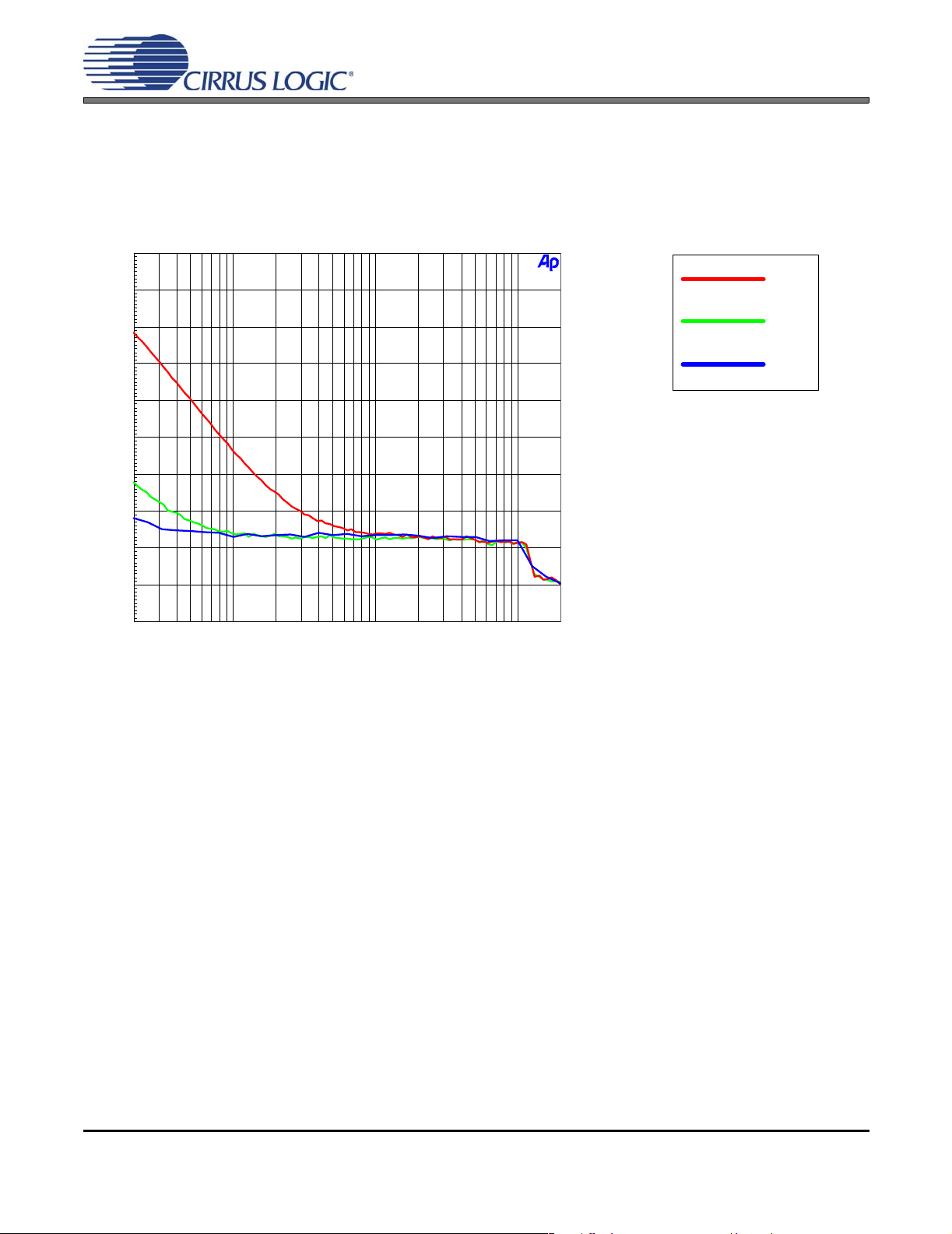
7.2 ADC_FILT+ Capacitor Effects on THD+N
60
The value of the capacitor on the ADC_FILT+ pin, 16, affects the low frequency total harmonic distortion +
noise (THD+N) performance of the ADC. Larger capacitor values yield significant improvement in THD+N
at low frequencies. Figure 32 shows the THD+N versus frequency for the ADC analog input. Plots were taken from the CDB42L51 using an Audio Precision analyzer.
-
CS42L51
-64
-68
-72
-76
d
B
-80
F
S
-84
-88
-92
-96
-100
20 20k50 100 200 500 1k 2k 5k 10k
Hz
Figure 32. ADC THD+N vs. Frequency w/Capacitor Effects
1 µF
10 µF
22 µF
Legend –
Capacitor Value on ADC_FILT+
74 DS679A2
8. EXAMPLE SYSTEM CLOCK FREQUENCIES
8.1 Auto Detect Enabled
CS42L51
Sample Rate
LRCK (kHz)
8 8.1920 12.2880 16.3840 24.5760
11 .025 11.2896 16.9344 22.5792 33.8688
12 12.2880 18.4320 24.5760 36.8640
1024x 1536x 2048x* 3072x*
MCLK (MHz)
Sample Rate
LRCK (kHz)
16 8.1920 12.2880 16.3840 24.5760
22.05 11.2896 16.9344 22.5792 33.8688
24 12.2880 18.4320 24.5760 36.8640
512x 768x 1024x* 1536x*
Sample Rate
LRCK (kHz)
32 8.1920 12.2880 16.3840 24.5760
44.1 11.2896 16.9344 22.5792 33.8688
48 12.2880 18.4320 24.5760 36.8640
256x 384x 512x* 768x*
Sample Rate
LRCK (kHz)
64 8.1920 12.2880 16.3840 24.5760
88.2 11.2896 16.9344 22.5792 33.8688
96 12.2880 18.4320 24.5760 36.8640
128x 192x 256x* 384x*
MCLK (MHz)
MCLK (MHz)
MCLK (MHz)
*The ”MCLKDIV2” pin 4 must be set HI.
DS679A2 75

8.2 Auto Detect Disabled
CS42L51
Sample Rate
LRCK (kHz)
8 - 6.1440 8.1920 12.2880 16.3840 24.5760
11 .025 - 8.4672 11.2896 16.9344 22.5792 33.8688
12 6.1440 9.2160 12.2880 18.4320 24.5760 36.8640
512x 768x 1024x 1536x 2048x 3072x
Sample Rate
LRCK (kHz)
16 - 6.1440 8.1920 12.2880 16.3840 24.5760
22.05 - 8.4672 11.2896 16.9344 22.5792 33.8688
24 6.1440 9.2160 12.2880 18.4320 24.5760 36.8640
256x 384x 512x 768x 1024x 1536x
Sample Rate
LRCK (kHz)
32 8.1920 12.2880 16.3840 24.5760
44.1 11.2896 16.9344 22.5792 33.8688
48 12.2880 18.4320 24.5760 36.8640
256x 384x 512x 768x
Sample Rate
LRCK (kHz)
64 8.1920 12.2880 16.3840 24.5760
88.2 11.2896 16.9344 22.5792 33.8688
96 12.2880 18.4320 24.5760 36.8640
128x 192x 256x 384x
MCLK (MHz)
MCLK (MHz)
MCLK (MHz)
MCLK (MHz)
76 DS679A2

9. PCB LAYOUT CONSIDERATIONS
9.1 Power Supply, Grounding
As with any high resolution converter, the CS42L51 requires careful attention to power supply and grounding
arrangements if its potential performance is to be realized. Figure 1 on page 10 shows the recommended
power arrangements, with VA and VA_HP connected to clean supplies. VD, which powers the digita l circuitry, may be run from the system logic supply. Alternatively, VD may be powered from the analog supply via
a ferrite bead. In this case, no additional devices should be powered from VD.
Extensive use of power and ground planes, ground plane fill in unused areas and surface mount decoupling
capacitors are recommended. Decoupling capa citors sh ould be as close to the pins of the
sible. The low value ceramic capacitor should be closest to the pin and should be mounted on the same
side of the board as the
kept away from the DAC_FILT+/ADC_FILT+ and VQ pins in order to avoid unwanted coupling into the modulators. The DAC_FILT+/ADC_FILT+ and VQ de co up lin g ca pacitors, particularly the 0.1 µF, must be positioned to minimize the electrical path from DAC_FILT+/ADC_FILT+ and AGND. The CDB42L51 e valuation
board demonstrates the optimum layout and power supply arrangements.
9.2 QFN Thermal Pad
The CS42L51 is available in a compact QFN package. The under side o f the QFN pa ckage reveals a la rge
metal pad that serves as a thermal relief to provide for maximum heat dissipation. This pad must mate with
an equally dimensioned copper pad on the PCB and must be electrically connected to ground. A series of
vias should be used to connect this copper pad to one or more larger ground planes on other PCB layers.
In split ground systems, it is recommended that this thermal pad be connected to AGND for best performance. The CS42L51 evaluation board demonstrates the op timum thermal pad and via configuration.
CS42L51 to minimize inductance effects . All signals, especially clocks, should be
CS42L51
CS42L51 as pos-
DS679A2 77
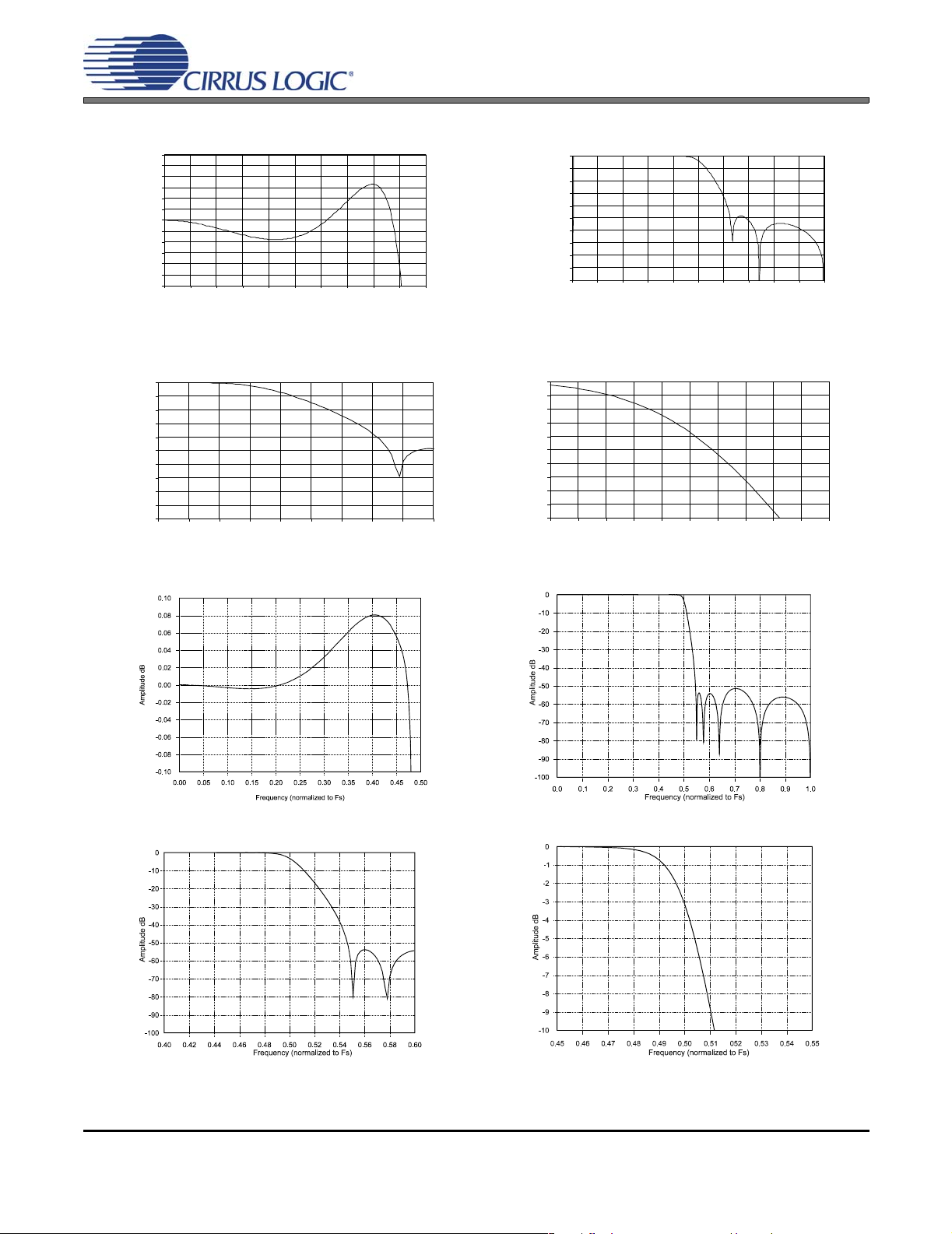
10.ADC & DAC DIGITAL FILTERS
CS42L51
0.3
0.25
0.2
0.15
0.1
0.05
0
-0.05
-0.1
Amplitude dB
-0.15
-0.2
-0.25
-0.3
0 0.05 0.1 0.15 0.2 0.25 0.3 0.35 0.4 0.45 0.5
Frequency (norma l iz ed to Fs)
0
-10
-20
-30
-40
-50
-60
Amplitude dB
-70
-80
-90
-100
0 0.1 0.2 0.3 0.4 0.5 0.6 0.7 0.8 0.9 1
Frequency (normalized to Fs)
Figure 33. ADC Passband Ripple Figure 34. ADC Stopband Rejection
0
-10
-20
-30
-40
-50
-60
Amplitude dB
-70
-80
-90
-100
0.4 0.43 0.46 0.49 0.52 0.55 0.58 0.61 0.64 0.67
Frequency (norma l i z ed to Fs)
0
-1
-2
-3
-4
-5
-6
Amplitude dB
-7
-8
-9
-10
0.45 0.46 0.47 0.48 0.49 0.5 0.51 0.52 0.53 0.54 0.55
Frequen cy (norma l iz ed to Fs)
Figure 35. ADC Transition Band Figure 36. ADC Transition Band
(Detail)
Figure 35. DAC Passband Ripple Figure 36. DAC Stopband
Figure 35. DAC Transition Band Figure 36. DAC Transition Band (Detail)
78 DS679A2

11.PARAMETER DEFINITIONS
Dynamic Range
The ratio of the rms value of the signal to the rms sum of all other spectral components over the specified
bandwidth. Dynamic Range is a signal-to-noise ratio measurement over the specified band width made with
a -60 dBFS signal. 60 dB is added to resulting measurement to refer the measurement to full-scale. This
technique ensures that the distortion components ar e below the n oise level an d do n ot affect the m easu rement. This measurement technique has been accepted by the Audio Engineering Society, AES17-1991,
and the Electronic Industries Association of Japan, EIAJ CP-307. Expressed in decibels.
Total Harmonic Distortion + Noise
The ratio of the rms value of the signal to the rms sum of all other spectral components over the specified
band width (typically 10 Hz to 20 kHz), including distortion components. Expressed in decibels. Measured
at -1 and -20 dBFS as suggested in AES17-1991 Annex A.
Frequency Response
A measure of the amplitude response variation from 10 Hz to 20 kHz relative to the amplitude response at
1 k Hz. Units in decibels.
Interchannel Isolation
A measure of crosstalk between the left and right channel pairs. Mea sured for ea ch channel at the co nverter's output with no signal to the input under test and a full-scale signa l applied to the other channel. Units in
decibels.
CS42L51
Interchannel Gain Mismatch
The gain difference between left and right channel pairs. Units in decibels.
Gain Error
The deviation from the nominal full-scale analog output for a full-scale digital input.
Gain Drift
The change in gain value with temperature. Units in ppm/°C.
Offset Error
The deviation of the mid-scale transition (111...111 to 000...000) from the ideal. Units in mV.
DS679A2 79

12.PACKAGE DIMENSIONS
32L QFN (5 X 5 mm BODY) PACKAGE DRAWING
CS42L51
e Pin #1 Corner
Pin #1 Corner
D
Top View
b
E
Side View
E2
A1
A
L
D2
Bottom View
INCHES MILLIMETERS NOTE
DIM MIN NOM MAX MIN NOM MAX
A----0.0394----1.001
A1 0.0000 -- 0.0020 0.00 -- 0.05 1
b 0.0071 0.0091 0.0110 0.18 0.23 0.28 1,2
D 0.1969 BSC 5.00 BSC 1
D2 0.1280 0.1299 0.1319 3.25 3.30 3.35 1
E 0.1969 BSC 5.00 BSC 1
E2 0.1280 0.1299 0.1319 3.25 3.30 3.35 1
e 0.0197 BSC 0.50 BSC 1
L 0.0118 0.0157 0.0197 0.30 0.40 0.50 1
JEDEC #: MO-220
Controlling Dimension is Millimeters.
1. Dimensioning and tolerance per ASME Y 14.5M-1995.
2. Dimensioning lead width applies to the plated terminal and is measured between 0.20 mm and 0.25 mm
from the terminal tip.
THERMAL CHARACTERISTICS
Parameter Symbol Min Typ Max Units
Junction to Ambient Thermal Impedance 2 Layer Board
4 Layer Board
80 DS679A2
θ
JA
-
-
52
38
-
-
°C/Watt
CS42L51
13.ORDERING INFORMATION
Product Description Package Pb-Free Grade Temp Range Container Order #
Rail CS42L51-CNZ
Tape & Reel CS42L51-CNZR
Rail CS42L51-DNZ
Tape & Reel CS42L51-DNZR
CS42L51
CDB42L51
CRD42L51
Low-Power Stereo
CODEC w/HP Amp for
Portable Apps
CS42L51 Evaluation
Board
CS42L51 Reference
Design
Commercial -10 to +70° C
32L-QFN Yes
Automotive -40 to +85° C
- No - - - CDB42L51
- No - - - CRD42L51
14.REFERENCES
1. C irr us Lo g i c, Audio Quality Measurement Specification, Version 1.0, 1997.
http://www.cirrus.com/products/papers/meas/meas.html
2. Cirrus Logic, AN18: Layout and Design Rules for Data Converters and Other Mixed Signal Devices,
Version 6.0, February 1998.
3. Cirru s Logic, Techniques to Measure and Maximize the Performance of a 120 dB, 96 kHz A/D Conv erter
Integrated Circuit, by Steven Harris, Steven Green and Ka Leung. Presented at the 103rd Co nvention of the
Audio Engineering Society, September 1997.
4. Cirrus Logic, A Stereo 16-bit Delta-Sigma A/D Converter for Digital Audio, by D.R. Welland, B.P. Del Signore, E.J. Swanson, T. Tanaka, K. Hamashita, S. Hara, K. Takasuka. Paper presented at the 85th Convention
of the Audio Engineering Society, November 1988.
5. Cirrus Logic, The Effects of Sampling Clock Jitter on Nyquist Sampling Analog-to-Digital Converters, and
on Oversampling Delta Sigma ADC's, by Steven Harris. Paper presented at the 87th Convention of the Audio Engineering Society, October 1989.
6. Cirrus Logic, An 18-Bit Dual-Channel Oversampling Delta-Sig ma A/D Converter, with 19-Bit M ono Applica-
tion Example, by Clif Sanchez. Paper presented at the 87th Convention of the Audio Engineering Society,
October 1989.
7. Cirrus Logic, How to Achieve Optimum Performance from Delta-Sigma A/D and D/A Converters, by Steven
Harris. Presented at the 93rd Convention of the Audio Engineering Society, October 1992.
8. Cirrus Logic, A Fifth-Order Delta-Sigma Modulator with 110 dB Audio Dynamic Range, by I. Fujimori, K. Hamashita and E.J. Swanson. Paper presented at the 93rd Convention of the Aud io Engineering Society, October 1992.
9. Philips Semiconductor, The I²C-Bus Specification: Version 2.1, January 2000.
http://www.semiconductors.philips.com
DS679A2 81

15.REVISION HISTORY
Rev. Date Changes
A1 May 2005 Initial Release subject to legal notice.
A2 September 2005 Renamed pin 14, FILT1+, to DAC_FILT+ and pin 16, FILT2+, to ADC_FILT+.
Added 1.5 µF capacitor recommendation to figure “Typical Connection Diagram (Software Mode)”
on page 10.
Removed the 0.1µF capacitors from pins DAC_FILT+, ADC_FILT+ and VQ on the figures “Typical
Connection Diagram (Software Mode)” on page 10 and “Typical Connection Diagram (Hardware
Mode)” on page 11.
Added DAC Isolation specification to “Analog Input Characteristics (Commercial - CNZ)” on
page 13 and “Analog Input Characteristics (Automotive - DNZ)” on page 14.
Corrected specification table “Headphone Output Power Characteristics” on page 19.
Removed t
page 20.
Added t
Serial Port” on page 20.
Adjusted timing specifications t
tion “Switching Specifications - Serial Port” on page 20.
Added MIC Bias PSRR specification to “DC Electrical Characteristics” on page 24.
Adjusted specification table “Power Consumption” on page 25.
Removed QSM clock ratios 128, 192, 256, 384 and HSM ratios 128, 192 from Table 3 on page 37.
Modified Digital Mix description in section “Digital Mix (DIGMIX)” on page 50.
Corrected DAC Zero Cross timeout period in section “Zero Cross” on page 56.
Adjusted BEEP off time settings in section “Beep Off Time (OFFTIME[2:0])” on page 61.
Modified BEEP description in section “Beep (BEEP)” on page 62.
Adjusted the minimum settings for the “Noise Gate Boost (NG_BOOST) and Threshold
(THRESH[3:0])” on page 70.
Swapped bits PCMA_OVFL w/PCMB_OVFL and ADCA_OVFL w/ADCB_OVFL in register “Status
(Address 20h) (Read Only)” on page 71.
Corrected Charge Pump Frequency setting in section “Charge Pump Frequency
(CHRG_FREQ[3:0])” on page 71.
Added sections “Headphone THD+N versus Output Power Plots” on page 72 and “ADC_FILT+
Capacitor Effects on THD+N” on page 74.
timing specification from table in section “Switching Specifications - Serial Port” on
d
s(SDO-SK)
and t
h(SK-SDO)
timing specification to table in section “Switching Specifications -
s(SD-SK)
from 0 ns to 20 ns and th from 50 ns to 20 ns in table in sec-
CS42L51
82 DS679A2

CS42L51
e
t
n
e
n
g
y
r
-
E
D
A
-
Y
r
ontacting Cirrus Logic Support
For all product questions and inquiries contact a Cirrus Logic Sales Representative.
o find the one nearest to you go to www.cirrus.com
MPORTANT NOTICE
Advance" product information describes prod ucts that are in development and subject to developm ent changes. Cirrus Logic, Inc. and its subsidiaries ("Cirrus") believ
hat the information contained in this document is accurate and reliable. However, the information is subject to change without notice and is provided "AS IS" withou
arranty of any kind (express or implied). Customers are advised to obtain the latest version of relevant information to verify, before placing orders, that informatio
eing relied on is current an d compl ete. All produ cts are so ld subject to the terms and cond itions of sa le supplie d at the time of order acknowledgment, including thos
ertaining to warranty, indem nific ation , an d lim ita tion o f lia bility. No respo nsibility is assum ed b y C irrus for th e u se of th is inform ati on, inc lud ing u se of this infor matio
s the basis for manufacture or sale of any items, or for infringement of patents or other rights of third parties. This document is the property of Cirrus and by furnishin
his information, Cirrus grants no license, express or implied under any patents, mask work rights, copyrights, trademarks, trade secrets or other intellectual propert
ights. Cirrus owns the copyrights associated with the information contained herein and gives consent for copies to be made of the information only for use within you
rganization with respect to Cirrus integrated circuits or other products of Cirrus. This consent does not extend to other cop ying such as copying for general distribu tion,
dvertising or promotional purposes, or for creating any work for resale.
ERTAIN APPLICATIONS USING SEMICONDUCTOR PRODUCTS MAY INVOLVE POTENTIAL RISKS OF DEATH, PERSONAL INJURY, OR SEVERE PROPER
Y OR ENVIRONMENTAL DAMAGE (“CRITICAL APPLICATIONS”). CIRRUS PRODUCTS ARE NOT DESIGNED, AUTHORIZED OR WARRANTED FOR USE IN
IRCRAFT SYSTEMS, MILITARY APPLICATIONS, PRODUCTS SURGICALLY IMPLANTED INTO THE BODY, AUTOMOTIVE SAFETY OR SECURITY DEVICES,
IFE SUPPORT PRODUCTS OR OTHER CRITICAL APPLICATIONS. INCLUSION OF CIRRUS PRODUCTS IN SUCH APPLICATIONS IS UNDERSTOOD TO B
ULLY AT THE CUSTOMER’S RISK AND CIRRUS DISCLAIMS AND MAKES NO WARRANTY, EXPRESS, STATUTORY OR IMPLIED, INCLUDING THE IMPLIE
ARRANTIES OF MERCHANTABILITY AND FITNESS FOR PARTICULAR PURPOSE, WITH REGARD TO ANY CIRRUS PRODUCT THAT IS USED IN SUCH
ANNER. IF THE CUSTOMER OR CUSTOMER’S CUSTOMER USES OR PERMITS THE USE OF CIRRUS PRODUCTS IN CRITICAL APPLICATIONS, CUSTOM
R AGREES, BY SUCH USE, TO FULLY INDEMNIFY CIRRUS, ITS OFFICERS, DIRECTORS, EMPLOYEES, DISTRIBUTORS AND OTHER AGENTS FROM AN
ND ALL LIABILITY, INCLUDING ATTORNEYS’ FEES AND COSTS, THAT MAY RESULT FROM OR ARISE IN CONNECTION WITH THESE USES.
irrus Logic, Cirrus, and the Cirrus Logic logo designs are trademarks of Cirrus Logic, Inc. All other brand and product names in this document may be trademarks o
ervice marks of their respective owners.
PI is a trademark of Motorola, Inc.
DS679A2 83
 Loading...