

CrystalClear SoundFusion™ Audio Codec ’97
Features
l AC ’97 2.1 Compatible
l Industry Leading Mixed Signal Technology
l 20-bit Stereo Digital-to-Analog Converters
l 18-bit Stereo Analog-to-Digital Converters
l Sample Rate Converters
l Four Analog Line-level Stereo Inputs for
LINE_IN, CD, VIDEO, and AUX
l Two Analog Line-level Mono Inputs for
Modem and Internal PC Beep
l Dual Stereo Line-level Outputs for
LINE_OUT and ALT_LINE_OUT
l Dual Microphone Inputs
l High Quality Pseudo-Differential CD Input
l Extensive Power Management Support
CS4299
l Meets or Exceeds the Microsoft
Audio Performance Requirements
l S/PDIF Digital Audio Output
l CrystalClear
3D Stereo Enhancement
Description
The CS4299 is an AC ’97 2.1 compatible stereo audio
codec designed for PC multimedia systems. Using the
industry leading CrystalClear
signal technology, the CS4299 enables the design of
PC 99-compliant desktop, portable, and entertainment
PCs.
Coupling the CS4299 with a PCI audio accelerator or
core logic supporting the AC ’97 interface, implements a
cost effective, superior quality, audio solution. The
CS4299 surpasses PC 99 and AC ’97 2.1 audio quality
standards.
ORDERING INFO
CS4299-KQ 48-pin TQFP 9x9x1.4 mm
CS4299-JQ 48-pin TQFP 9x9x1.4 mm
delta-sigma and mixed
PC 99
AC-LINK AND AC’97
REGISTERS
PWR
MGT
SYNC
BIT_CLK
SDATA_OUT
SDATA_IN
RESET#
AC-
LINK
AC’97
REGISTERS
S/PDIF
Preliminary Product Information
P.O. Box 17847, Austin, Texas 78760
(512) 445 7222 FAX: (512) 445 7581
http://www.cirrus.com
ANALOG INPUT MUX
AND OUTPUT MIXER
LINE
CD
AUX
ADC
DAC
INPUT
MUX
OUTPUT
MIXER
Σ
SRC
GAIN / MUTE CONTROLS
MIXER / MUX SELECTS
SRC
This document contains information for a new product.
Cirrus Logic reserves the right to modify this product without notice.
PCM_DATA
PCM_DATA
Copyright Cirrus Logic, Inc. 2001
(All Rights Reserved)
18 bits
20 bits
VIDEO
MIC1
MIC2
PHONE
PC_BEEP
LINE_OUT
ALT_LINE_OUT
MONO_OUT
JUN ‘01
DS319PP5
1

TABLE OF CONTENTS
1. CHARACTERISTICS AND SPECIFICATIONS .................................................................5
Analog Characteristics ........................................................................................................5
Mixer Characteristics ..........................................................................................................6
Absolute Maximum Ratings ................................................................................................6
Recommended Operating Conditions.................................................................................6
Digital Characteristics .........................................................................................................6
AC ’97 Serial Port Timing....................................................................................................7
2. GENERAL DESCRIPTION ...............................................................................................10
2.1 AC-Link ....................................................................................................................10
2.2 Control registers ......................................................................................................10
2.3 Output Mixer .............................................................................................................11
2.4 Input Mux .................................................................................................................11
2.5 Volume Control ........................................................................................................11
3. AC LINK FRAME DEFINITION .........................................................................................13
3.1 AC-Link Serial Data Output Frame ..........................................................................14
3.1.1 Serial Data Output Slot Tags (Slot 0) ...........................................................14
3.1.2 Command Address Port (Slot 1) ..................................................................15
3.1.3 Command Data Port (Slot 2) ........................................................................15
3.1.4 PCM Playback Data (Slots 3-10) .................................................................15
3.2 AC-Link Audio Input Frame ......................................................................................16
3.2.5 Serial Data Input Slot Tag Bits (Slot 0) .......................................................16
3.2.6 Status Address Port (Slot 1) .........................................................................16
3.2.7 Status Data Port (Slot 2) ..............................................................................17
3.2.8 PCM Capture Data (Slot 3-10) .....................................................................17
3.3 AC-Link Protocol Violation - Loss of SYNC ..............................................................18
4. REGISTER INTERFACE ..................................................................................................19
4.3 Reset Register (Index 00h) ......................................................................................20
4.4 Master Volume Register (Index 02h) .......................................................................20
4.5 Alternate Volume Register (Index 04h) ....................................................................21
4.6 Mono Volume Register (Index 06h) .........................................................................21
4.7 PC_BEEP Volume Register (Index 0Ah) .................................................................22
4.8 Phone Volume Register (Index 0Ch) ........................................................................22
4.9 Microphone Volume Register (Index 0Eh) ................................................................23
CS4299
Contacting Cirrus Logic Support
For a complete listing of Direct Sales, Distributor, and Sales Representative contacts, visit the Cirrus Logic web site at:
http://www.cirrus.com/corporate/contacts/sales.cfm
Microsoft is a registered trademark of Microsoft Corporation in the United States and/or other countries.
Intel is a registered trademark of Intel Corporation.
Crystal Clear and Sound Fusion are trademarks of Cirrus Logic.
Preliminary product information describes products which are in production, but for which full characterization data is not yet available. Advance product information describes products which are in development and subject to development changes. Cirrus Logic, Inc. has made best efforts to ensure that the information contained in this document is accurate and reliable. However, the information is subject to change without notice and is provided “AS IS” without
warranty of any kind (express or implied). No responsibility is assumed by Cirrus Logic, Inc. for the use of this information, nor for infringements of patents or
other rights of third parties. This document is the property of Cirrus Logic, Inc. and implies no license under patents, copyrights, trademarks, or trade secrets.
No part of this publication may be copied, reproduced, stored in a retrieval system, or transmitted, in any form or by any means (electronic, mechanical, photographic, or otherwise) without the prior written consent of Cirrus Logic, Inc. Items from any Cirrus Logic website or disk may be printed for use by the user.
However, no part of the printout or electronic files may be copied, reproduced, stored in a retrieval system, or transmitted, in any form or by any means (electronic, mechanical, photographic, or otherwise) without the prior written consent of Cirrus Logic, Inc.Furthermore, no part of this publication may be used as a
basis for manufacture or sale of any items without the prior written consent of Cirrus Logic, Inc. The names of products of Cirrus Logic, Inc. or other vendors
and suppliers appearing in this document may be trademarks or service marks of their respective owners which may be registered in some jurisdictions. A list
of Cirrus Logic, Inc. trademarks and service marks can be found at http://www.cirrus.com.
2

4.10 Stereo Analog Mixer Input Gain Registers (Index 10h - 18h) ................................. 24
4.11 Input Mux Select Register (Index 1Ah) ................................................................... 25
4.12 Record Gain Register (Index 1Ch) ......................................................................... 25
4.13 General Purpose Register (Index 20h) ................................................................... 26
4.14 3D Control Register (Index 22h) .............................................................................26
4.15 Powerdown Control/Status Register (Index 26h) ...................................................27
4.16 Extended Audio ID Register (Index 28h) ................................................................ 28
4.17 PCM Front DAC Rate Register (Index 2Ch) ........................................................ 28
4.18 PCM L/R ADC Rate Register (Index 32h) .............................................................. 28
4.19 AC Mode Control Register (Index 5Eh) .................................................................. 29
4.20 Misc. Crystal Control Register (Index 60h) ............................................................. 29
4.21 S/PDIF Control Register (Index 68h) ..................................................................... 30
4.22 Vendor ID1 Register (Index 7Ch) ........................................................................... 31
4.23 Vendor ID2 Register (Index 7Eh) ........................................................................... 31
5. POWER MANAGEMENT ................................................................................................. 32
5.1 AC ’97 Reset Modes ................................................................................................ 32
5.1.1 Cold AC ‘97 Reset ....................................................................................... 32
5.1.2 Warm AC ’97 Reset ..................................................................................... 32
5.1.3 Register AC ’97 Reset ................................................................................. 32
5.2 Powerdown Controls ................................................................................................ 33
6. ANALOG HARDWARE DESCRIPTION ......................................................................... 35
6.1 Analog Inputs ........................................................................................................... 35
6.1.4 Line-Level Inputs ........................................................................................ 35
6.1.5 CD Input ..................................................................................................... 35
6.1.6 Microphone Inputs ...................................................................................... 36
6.1.7 PC Beep Input ............................................................................................36
6.1.8 Phone Input ................................................................................................37
6.2 Analog Outputs ........................................................................................................ 37
6.2.9 Stereo Outputs ........................................................................................... 37
6.2.10 Mono Output .............................................................................................37
6.3 Miscellaneous Analog Signals .................................................................................38
6.4 Power Supplies ........................................................................................................ 38
6.5 Reference Design ....................................................................................................38
7. SONY/PHILIPS DIGITAL INTERFACE (S/PDIF) ............................................................ 39
8. GROUNDING AND LAYOUT .......................................................................................... 39
9. PIN DESCRIPTIONS 41
10. PARAMETER AND TERM DEFINITIONS ....................................................................46
11. REFERENCE DESIGN ................................................................................................. 48
12. REFERENCES .............................................................................................................. 49
13. PACKAGE DIMENSIONS ............................................................................................. 50
CS4299
LIST OF FIGURES
Figure 1. Power Up Timing .......................................................................................................8
Figure 2. Codec Ready from Startup or Fault Condition........................................................... 8
Figure 3. Clocks ........................................................................................................................ 8
Figure 4. Data Setup and Hold.................................................................................................. 9
Figure 5. PR4 Powerdown and Warm Reset ............................................................................ 9
Figure 6. Test Mode .................................................................................................................. 9
Figure 7. AC-link Connections ................................................................................................10
Figure 8. Mixer Diagram.......................................................................................................... 12
Figure 9. AC-link Input and Output Framing ........................................................................... 13
Figure 10. Line Input (Replicate for Video and Aux) ...............................................................35
3

Figure 11. Differential 2 VRMS CD Input ................................................................................35
Figure 12. Differential 1 VRMS CD Input ................................................................................35
Figure 13. Microphone Input ...................................................................................................36
Figure 14. Microphone Pre-amplifier .......................................................................................36
Figure 15. PC_BEEP Input......................................................................................................36
Figure 16. Modem Connection ................................................................................................37
Figure 17. Alternate Line Output as Headphone Output .........................................................37
Figure 18. Stereo Output .........................................................................................................37
Figure 19. Voltage Regulator ..................................................................................................38
Figure 20. S/PDIF Output ........................................................................................................39
Figure 21. Conceptual Layout for the CS4297A......................................................................40
Figure 22. Pin Locations for the CS4297A ..............................................................................41
Figure 23. CS4297A Reference Design ..................................................................................48
LIST OF TABLES
Table 1. Mixer Registers .........................................................................................................19
Table 2. Analog Mixer Output Attenuation ..............................................................................21
Table 3. Microphone Input Gain Values ..................................................................................23
Table 4. Analog Mixer Input Gain Values................................................................................24
Table 5. Stereo Volume Register Index ..................................................................................24
Table 6. Input Mux Selection...................................................................................................25
Table 7. Slot Mapping ............................................................................................................29
Table 8. Device ID with Corresponding Part Number .............................................................31
Table 9. Revision Values.........................................................................................................31
Table 10. Powerdown PR Bit Functions..................................................................................33
Table 11. Powerdown PR Function Matrix ..............................................................................34
Table 12. Power Consumption by Powerdown Mode .............................................................34
CS4299
4
1. CHARACTERISTICS AND SPECIFICATIONS
CS4299
ANALOG CHARACTERISTICS Standard test conditions unless otherwise noted: T
AVdd = 5.0 V ±5%, DVdd = 3.3 V ±5%; 1 kHz Input Sine wave; Sample Frequency, Fs = 48 kHz; Z
1000 pF load, C
= 18 pF load (Note 1); Measurement bandwidth is 20 Hz - 20 kHz, 18-bit linear coding for ADC
DL
ambient
=100 kΩ/
AL
= 25° C,
functions, 20-bit linear coding for DAC functions; Mixer registers set for unity gain.
CS4299-KQ CS4299-JQ
Parameter
(Note 2)
Symbol Path
(Note 3)
UnitMin Typ Max Min Typ Max
Full Scale Input Voltage
Line Inputs
Mic Inputs
Mic Inputs (20 dB internal gain)
A-D
A-D
A-D
0.91
0.91
0.091
1.00
1.00
0.10
-
0.91
-
0.91
-
0.091
1.00
1.00
0.10
-
V
V
V
RMS
RMS
RMS
-
-
Full Scale Output Voltage
Line,Alternate Line, and Mono Outputs D-A 0.91 1.0 1.13 0.91 1.0 1.13 V
Frequency Response (Note 4)
Analog Ac = ± 0.25 dB
DAC Ac = ± 0.25 dB
ADC Ac = ± 0.25 dB
Dynamic Range
Stereo Analog inputs to LINE_OUT
Mono Analog inputs to LINE_OUT
DAC Dynamic Range
ADC Dynamic Range
DAC SNR (-20 dB FS input w/
CCIR-RMS filter on output)
Total Harmonic Distortion + Noise
FR
DR
SNR
THD+N
A-A
D-A
A-D
A-A
A-A
D-A
A-D
20
20
20
90
85
85
85
95
90
90
90
-
-
-
20,000
20,000
20,000
-
-
-
-
20
20
20
-
20,000
-
20,000
-
20,000
90
85
87
85
-
-
-
-
-
D-A-70---- dB
RMS
Hz
Hz
Hz
dB FS A
dB FS A
dB FS A
dB FS A
(-3 dB FS input signal):
Line/Alternate Line Output
DAC
ADC (all inputs except phone/mic)
ADC (phone/mic)
A-A
D-A
A-D
A-D
-74
-90
-
-91
-
-88
-
-84
-
-80
-80
-80
-74
-
-
-
-
-
-74
-
-74
-
-74
-
dB FS
dB FS
dB FS
dB FS
Power Supply Rejection Ratio
(1 kHz, 0.5 V
w/ 5 V DC offset)(Note 4) 40 60 - - 40 - dB
RMS
Interchannel Isolation 70 88 - - 88 - dB
Spurious Tone (Note 4) - -100 - - -100 - dB FS
Input Impedance (Note 4) 10 - - 10 - - kΩ
External Load Impedance 10 - - 10 - - kΩ
Output Impedance (Note 4) - 730 - - 730 - Ω
Input Capacitance (Note 4) - 5 - - 5 - pF
Vrefout 2.0 2.28 2.5 2.0 2.28 2.5 V
Notes: 1. Z
2. Parameter definitions are given in the Section 10, Parameter and Term Definitions.
3. Path refers to the signal path used to generate this data. These paths are defined in the Section 10,
4. This specification is guaranteed by silicon characterization, it is not production tested.
refers to the analog output pin loading and CDL refers to the digital output pin loading.
AL
Parameter and Term Definitions.
5
CS4299
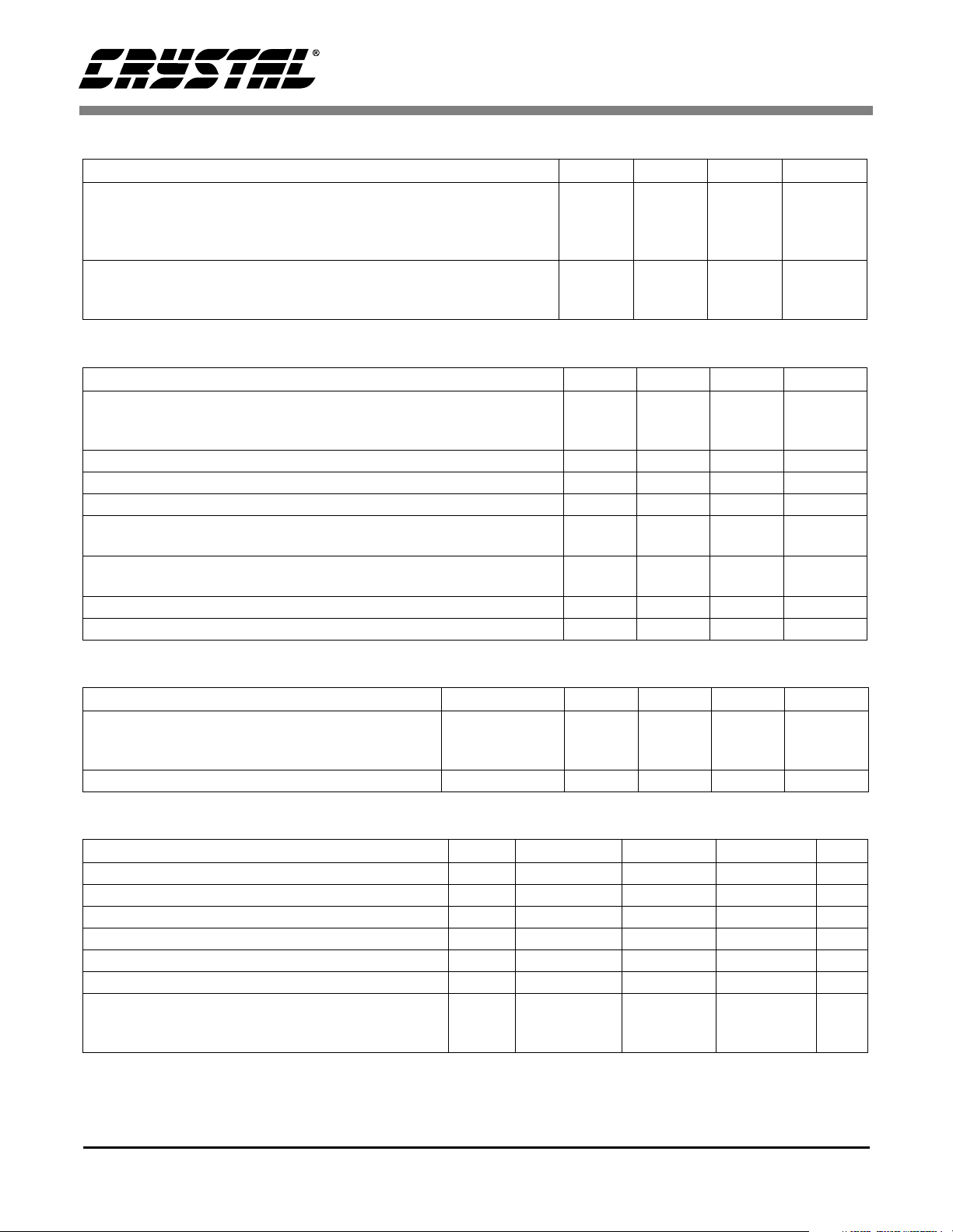
MIXER CHARACTERISTICS (for CS4299-KQ only)
Parameter Min Typ Max Unit
Mixer Gain Range Span
Line In, Aux, CD, Video, Mic1, Mic2, Phone, PC Beep
Mono Out, Alternate Line Out
Line Out
Step Size
All volume controls except PC Beep
PC Beep
ABSOLUTE MAXIMUM RATINGS (AVss1 = AVss2 = DVss1 = DVss2 = 0 V)
Parameter Min Typ Max Unit
Power Supplies +3.3 V Digital
+5 V Digital
Analog
Total Power Dissipation (Supplies, Inputs, Outputs) - - 1.25 W
Input Current per Pin (Except Supply Pins) -10 - 10 mA
Output Current per Pin (Except Supply Pins) -15 - 15 mA
Analog Input voltage -0.3 - AVdd+
Digital Input voltage -0.3 - DVdd +
Ambient Temperature (Power Applied) -55 - 110 °C
Storage Temperature -65 - 150 °C
-
-
-
-
-
-0.3
-0.3
-0.3
46.5
46.5
94.5
1.5
3.0
-
-
-
-
-
-
-
-
6.0
6.0
6.0
0.3
0.3
dB
dB
dB
dB
dB
V
V
V
V
V
RECOMMENDED OPERATING CONDITIONS (AVss1 = AVss2 = DVss1 = DVss2 = 0 V)
Parameter Symbol Min Typ Max Unit
Power Supplies +3.3 V Digital
+5 V Digital
Analog
Operating Ambient Temperature 0 - 70 °C
DVdd1, DVdd2
DVdd1, DVdd2
AVdd1, AVdd2
3.135
4.75
4.75
3.3
5
5
3.465
5.25
5.25
V
V
V
DIGITAL CHARACTERISTICS (AVss = DVss = 0 V)
Parameter Symbol Min Typ Max Unit
Low level input voltage V
High level input voltage V
High level output voltage V
Low level output voltage V
Input Leakage Current (AC-link inputs) -10 - 10 µA
Output Leakage Current (Tri-stated AC-link outputs) -10 - 10 µA
Output buffer drive current
BIT_CLK, S/PDIF_OUT
SDATA_IN, EAPD (Note 4)
il
ih
oh
ol
- -0.8V
0.65 x DVdd - - V
0.90 x DVdd 0.99 x DVdd - V
- 0.03 0.10 x DVdd V
-
-
24
-
4
-
mA
mA
6
CS4299
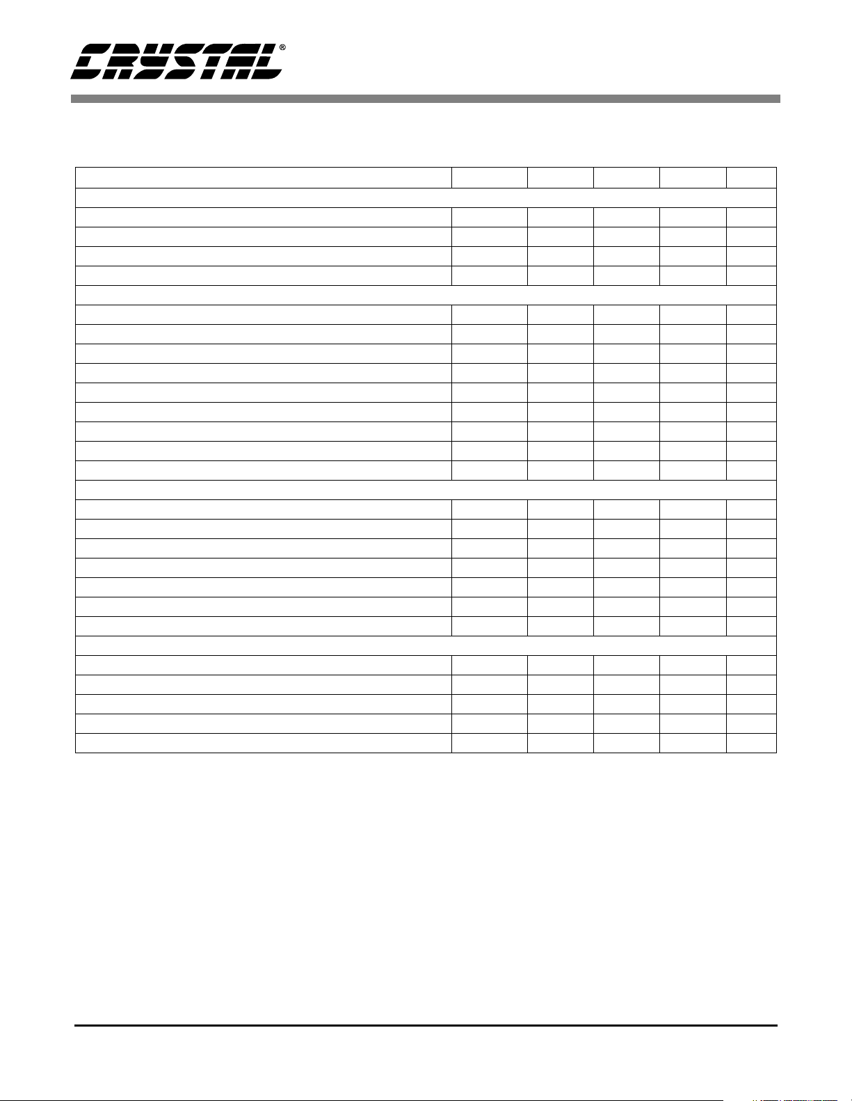
AC ’97 SERIAL PORT TIMING Standard test conditions unless otherwise noted: T
AVdd = 5.0 V, DVdd = 3.3 V; C
= 55 pF load.
L
ambient
= 25° C,
Parameter Symbol Min Typ Max Unit
RESET Timing
RESET# active low pulse width T
RESET# inactive to BIT_CLK start-up delay T
1st SYNC active to CODEC READY set T
Vdd stable to Reset inactive T
rst_low
rst2clk
sync2crd
vdd2rst#
1.0 - - µs
- 40.0 - µs
- 62.5 - µs
100 - - µs
Clocks
BIT_CLK frequency F
BIT_CLK period T
clk_period
clk
- 12.288 - MHz
- 81.4 - ns
BIT_CLK output jitter (depends on XTAL_IN source) - - 750 ps
BIT_CLK high pulse width T
BIT_CLK low pulse width T
SYNC frequency F
SYNC period T
SYNC high pulse width T
SYNC low pulse width T
sync_period
sync_high
sync_low
clk_high
clk_low
sync
36 40.7 45 ns
36 40.7 45 ns
-48-kHz
- 20.8 - µs
-1.3-µs
- 19.5 - µs
Data Setup and Hold
Output Propagation delay from rising edge of BIT_CLK T
Input setup time from falling edge of BIT_CLK T
Input hold time from falling edge of BIT_CLK T
Input Signal rise time T
Input Signal fall time T
Output Signal rise time (Note 4) T
Output Signal fall time (Note 4) T
co
isetup
ihold
irise
ifall
orise
ofall
81012ns
10 - - ns
0--ns
2-6ns
2-6ns
246ns
246ns
Misc. Timing Parameters
End of Slot 2 to BIT_CLK, SDATA_IN low (PR4) T
SYNC pulse width (PR4) Warm Reset T
SYNC inactive (PR4) to BIT_CLK start-up delay T
Setup to trailing edge of RESET# (ATE test mode) (Note 4) T
s2_pdown
sync_pr4
sync2clk
setup2rst
Rising edge of RESET# to Hi-Z delay (Note 4) T
off
-.281.0µs
1.0 - - µs
162.8 285 - ns
15 - - ns
- - 25 ns
7
BIT_CLK
CS4299
RESET#
Vdd
BIT_CLK
SYNC
CODEC_READY
T
rst_low
T
vdd2rst#
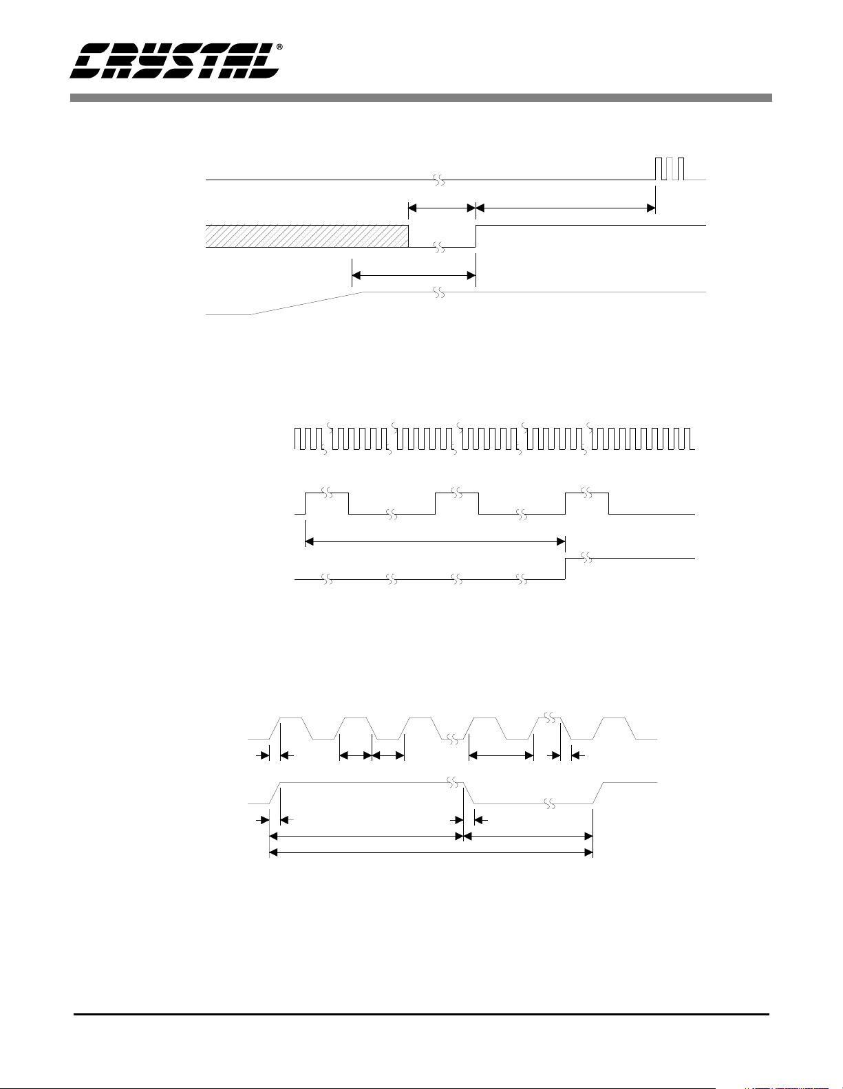
Figure 1. Power Up Timing
T
sync2crd
T
rst2clk
BIT_CLK
T
orise
SYNC
T
irise
Figure 2. Codec Ready from Startup or Fault Condition
T
clk_highTclk_low
T
sync_high
T
Figure 3. Clocks
T
ifall
sync_period
T
clk_period
T
sync_low
T
ifall
8
BIT_CLK
BIT_CLK
SDATA_IN
SDATA_OUT,
SYNC
Slot 1 Slot 2
T
co
T
isetup
Figure 4. Data Setup and Hold
T
CS4299
ihold
SDATA_OUT
SDATA_IN
SYNC
Write to 0x20 Data PR4 Don’t Care
T
s2_pdown
T
Figure 5. PR4 Powerdown and Warm Reset
RESET#
T
setup2rst
SDATA_OUT,
SYNC
T
off
sync_pr4
T
sync2clk
SDATA_IN,
BIT_CLK
Hi-Z
Figure 6. Test Mode
9

CS4299
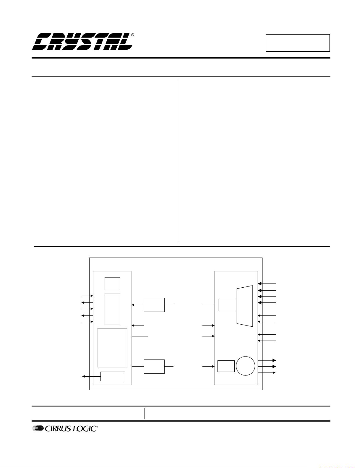
2. GENERAL DESCRIPTION
The CS4299 is a mixed-signal serial audio Codec
compliant to the Intel® Audio Codec ‘97 Specifica-
tion, revision 2.1 [1]. It is designed to be paired
with a digital controller, typically located on the
PCI bus or integrated within the system core logic
chip set. The controller is responsible for all communications between the CS4299 and the remainder of the system. The CS4299 contains two
distinct functional sections: digital and analog. The
digital section includes the AC-link interface,
S/PDIF interface, serial data port, Sample Rate
Converters, and power management support. The
analog section includes the analog input multiplexer (mux), stereo output mixer, mono output mixer,
stereo Analog-to-Digital Converters (ADCs), stereo Digital-to-Analog Converters (DACs), and
their associated volume controls.
2.1 AC-Link
All communication with the CS4299 is established
with a 5-wire digital interface to the controller, as
shown in Figure 7. This interface is called the
AC-link. All clocking for the serial communication
is synchronous to the BIT_CLK signal. BIT_CLK
is generated by the primary audio codec and is used
to clock the controller and any secondary audio co-
decs. Both input and output AC-link audio frames
are organized as a sequence of 256 serial bits forming 13 groups referred to as ‘slots’. During each audio frame, data is passed bi-directionally between
the CS4299 and the controller. The input frame is
driven from the CS4299 on the SDATA_IN line.
The output frame is driven from the controller on
the SDATA_OUT line. The controller is also responsible for issuing reset commands via the RESET# signal. Following a Cold Reset, the CS4299
is responsible for notifying the controller that it is
ready for operation after synchronizing its internal
functions. The CS4299 AC-link signals must use
the same digital supply voltage as the controller
chip, either +5 V or +3.3 V. See Section 3, AC Link
Frame Definition, for detailed AC-link information.
2.2 Control registers
The CS4299 contains a set of AC ’97 compliant
control registers and a set of Cirrus Logic defined
control registers. These registers control the basic
functions and features of the CS4299. Read accesses of the control registers by the AC ’97 controller
are accomplished with the requested register index
in Slot 1 of a SDATA_OUT frame. The following
SDATA_IN frame will contain the read data in its
10
Digital AC’97
Controller
Figure 7. AC-link Connections
SYNC
BIT_CLK
SDATA_OUT
SDATA_IN
RESET#
CODEC

CS4299
Slot 2. Write operations are similar, with the register index in Slot 1 and the write data in Slot 2 of a
SDATA_OUT frame. The function of each input
and output frame is detailed in Section 3, AC Link
Frame Definition. Individual register descriptions
are found in Section 4, Register Interface.
2.3 Sample Rate Converters
The Sample Rate Converters (SRCs) provide high
accuracy digital filters supporting sample frequencies other than 48 kHz to be captured from the
CS4299 or played from the controller. AC ’97 requires support for two audio rates (44.1 and
48kHz). In addition, the Intel® I/O Controller Hub
(ICHx) specification requires support for five more
audio rates (8, 11.025, 16, 22.05, and 32). The
CS4299 supports all these rate, as shown in Table 7
on page 29.
2.4 Output Mixer
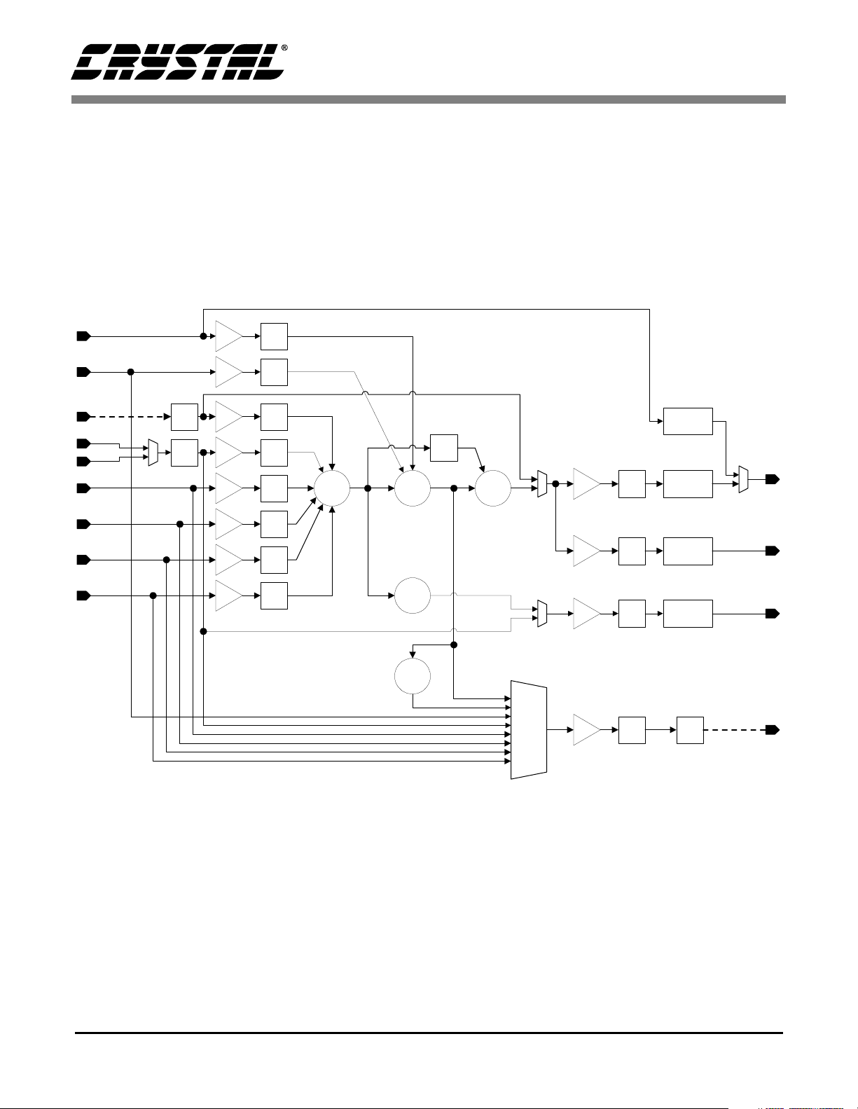
The CS4299 has two output mixers, illustrated in
Figure 8. The stereo output mixer sums together
the analog inputs to the CS4299, including the
PC_BEEP and PHONE signals, according to the
settings in the volume control registers. The stereo
output mix is sent to the LINE_OUT and
ALT_LINE_OUT pins on the CS4299. The mono
output mixer generates a monophonic sum of the
left and right channels from the stereo input mixer.
The mono output mix is sent to the MONO_OUT
output pin on the CS4299.
2.5 Input Mux
The input multiplexer controls which analog input
is sent to the ADCs. The output of the input mux is
converted to stereo 18-bit digital PCM data and
sent to the controller by means of the AC-link
SDATA_IN signal.
2.6 Volume Control
The CS4299 volume registers control analog input
levels to the input mixer and analog output levels,
including the master volume level, and the alternate
volume level. The PC_BEEP volume control uses
3 dB steps with a range of 0 dB to -45 dB attenuation. All other analog volume controls use 1.5 dB
steps. The analog inputs have a mixing range of
+12 dB signal gain to -34.5 dB signal attenuation.
The analog output volume controls have from 0 dB
to -94.5 dB attenuation for LINE_OUT and from
0 dB to -46.5 dB attenuation for ALT_LINE_OUT
and MONO_OUT.
11
CS4299
PC_BEEP
PHONE
PCM_OUT
MIC1
MIC2
LINE
CD
VIDEO
AUX
MIC
SELECT
MAIN D/A
CONVERTERS
DAC
BOOST
VOL
VOL
VOL
VOL VOL
VOL VOL VOL
MUTE
MUTE
MUTE
MUTE
MUTE
MUTE
MUTE
MUTE
PC BEEP BYPASS
Σ Σ
INPUT MIXER
ANALOG STEREO
Σ
ANALOG STEREO
OUTPUT MIXER
STEREO TO
MONO MIXER
Σ
1/2
STEREO TO
MONO MIXER
Σ
1/2
BYPASS
BUFFER
3D
3D OUTPUT
MIXER
DAC DIRECT
MONO OUT
ADC
INPUT
MUX
MODE
SELECT
MASTER
VOLUME
VOL VOL
ALT LINE
VOLUME
MONO
VOLUME
VOL
MAIN ADC
GAIN
VOL
MUTE
MUTE
MUTE
OUTPUT
BUFFER
OUTPUT
BUFFER
OUTPUT
BUFFER
MAIN A/D
CONVERTERS
ADCMUTE
LINE OUT
ALT LINE OUT
MONO OUT
PCM_IN
12
Figure 8. Mixer Diagram
CS4299
3. AC LINK FRAME DEFINITION
The AC-link is a bidirectional serial port with data
organized into frames consisting of one 16-bit and
twelve 20-bit time-division multiplexed slots. The
first slot, called the tag slot, contains bits indicating
if the CS4299 is ready to receive data (input frame)
and which, if any, other slots contain valid data.
Slots 1 through 12 contain audio or control/status
data. Both the serial data output and input frames
are defined from the controller perspective, not
from the CS4299 perspective.
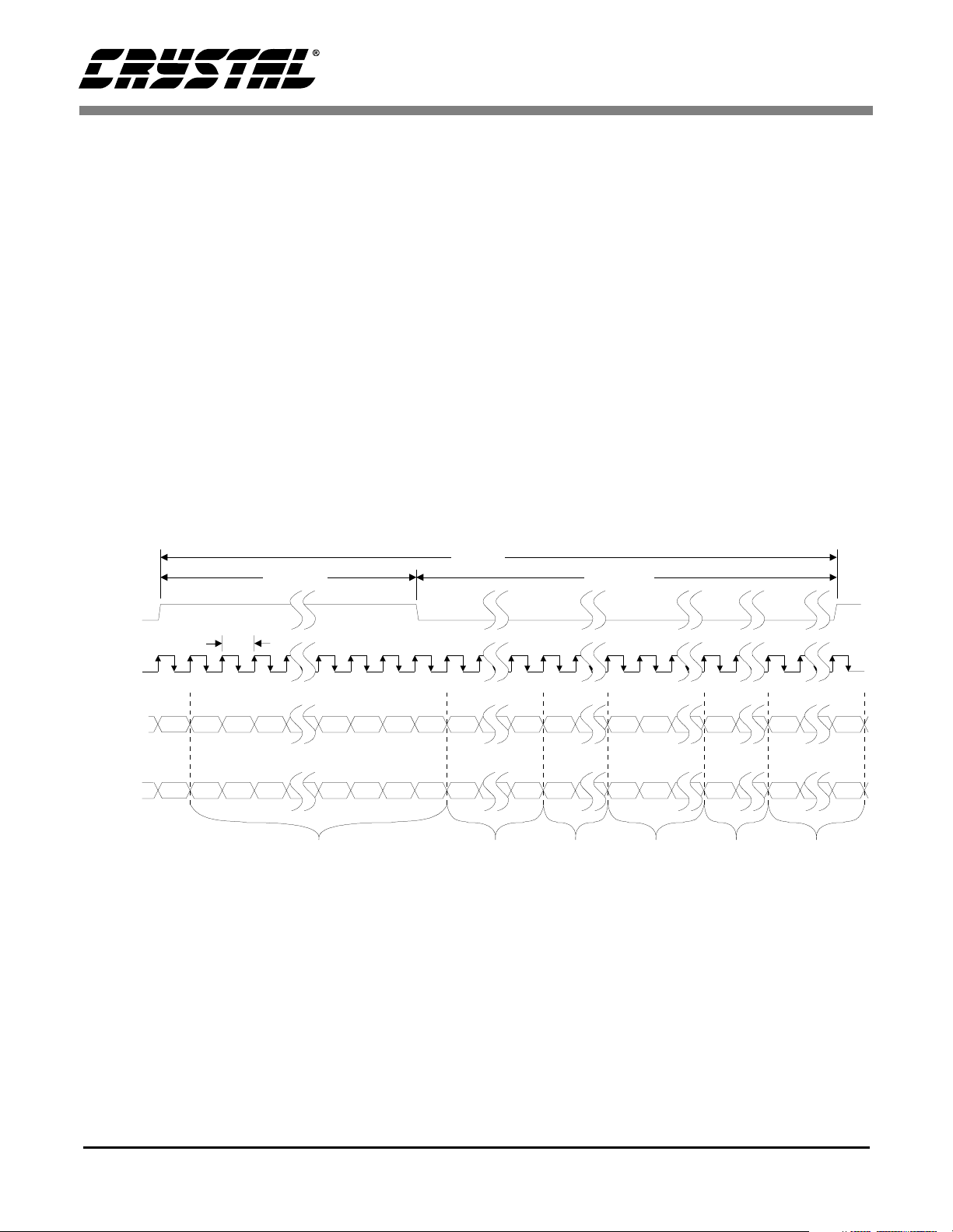
The controller synchronizes the beginning of a
frame with the assertion of the SYNC signal.
Tag Phase Data Phase
Figure 9 shows the position of each bit location
within the frame. The first bit position in a new se-
rial data frame is F0 and the last bit position in the
serial data frame is F255. When SYNC goes active
(high) and is sampled active by the CS4299 (on the
falling edge of BIT_CLK), both devices are syn-
chronized to a new serial data frame. The data on
the SDATA_OUT pin at this clock edge is the final
bit of the previous frame’s serial data. On the next
rising edge of BIT_CLK, the first bit of Slot 0 is
driven by the controller on the SDATA_OUT pin.
On the next falling edge of BIT_CLK, the CS4299
latches this data in, as the first bit of the frame.
20.8 µs
(48 kHz)
SYNC
BIT_CLK
Bit Frame Position:
SDATA_OUT
Bit Frame Position:
SDATA_IN
12.288 MHz
81.4 ns
F0 F1 F2 F16F15F14F13F12
F255
Valid
Frame
F0 F1 F2 F16F15F14F13F12 F35 F56 F76F255
Codec
Ready
Slot 1
Valid
Slot 1
Valid
GPIO
INT
0
Slot 2
Valid
Slot 2
Valid
F36 F57
Slot 12
Valid
Slot 12
Valid
Slot 0 Slot 1 Slot 2 Slot 3 Slot 4 Slots 5-12
Codec
Codec
0
ID1
R/W 0 WD15
ID0
0000
F35
F36
0
F56
D19 D18
F57
D19 D18 D19RD15
F76
D19
F96
D19
F96
D19
Figure 9. AC-link Input and Output Framing
F255
F255
GPIO
0
INT
13

CS4299
3.1 AC-Link Serial Data Output Frame
In the serial data output frame, data is passed on the SDATA_OUT pin to the CS4299 from the AC ’97
controller. Figure 9 illustrates the serial port timing.
The PCM playback data being passed to the CS4299 is shifted out MSB first in the most significant bits
of each slot. Any PCM data from the AC ’97 controller that is not 20 bits wide should be left justified in
its corresponding slot and dithered or zero-padded in the unused bit positions.
Bits that are reserved should always be ‘cleared’ by the AC ’97 controller.
3.1.1 Serial Data Output Slot Tags (Slot 0)
Bit 1514131211109876543210
Val id
Slot 1
Frame
Valid Frame The Valid Frame bit determines if any of the following slots contain either valid playback data
Slot [1:2] Valid The Slot [1:2] Valid bits indicate the validity of data in their corresponding serial data output
Valid
Slot 2
Valid
Slot 3
Valid
Slot 4
Valid
Slot 5
Valid
Slot 6
Valid
Slot 7
Valid
Slot 8
Valid
Slot 9
Valid
Slot 10
Valid
Reserved
Codec
for the CS4299 DACs or data for read/write operations. When ‘set’, at least one of the other
AC-link slots contain valid data. If this bit is ‘clear’, the remainder of the frame is ignored.
slots. If a bit is ‘set’, the corresponding output slot contains valid data. If a bit is ‘cleared’, the
corresponding slot will be ignored.
ID1
Codec
ID0
Slot [3:10] Valid The Slot [3:10] Valid bits indicate Slot [3:10] contains valid playback data for the CS4299. If a
Slot Valid bit is ‘set’, the named slot contains valid audio data. If the bit is ‘clear’, the slot will be
ignored. The CS4299 supports alternate slot mapping as defined in the AC ’97 2.1 specification.
For more information, see the AC Mode Control Register (Index 5Eh).
Codec ID[1:0] The Codec ID[1:0] bits display the Codec ID of the audio codec being accessed during the cur-
rent AC-link frame. Codec ID[1:0] = 00 indicates the primary codec is being accessed. Codec
ID[1:0] = 01, 10, or 11 indicates one of three possible secondary codecs is being accessed. A
non-zero value of one or more of the Codec ID bits indicates a valid Read or Write Address in
Slot 1, and the Slot 1 R/W bit indicates presence or absence of valid Data in Slot 2.
14

CS4299
3.1.2 Command Address Port (Slot 1)
Bit 191817161514131211109876543210
R/W RI6RI5RI4RI3RI2RI1RI0000000000000
R/W Read/Write. When this bit is ‘set’, a read of the AC ’97 register specified by the register index
bits will occur in the AC ’97 2.1 audio codec. When the bit is ‘cleared’, a write will occur. For any
read or write access to occur, the Frame Valid bit (F0) must be ‘set’ and the Codec ID[1:0] bits
(F[14:15]) must match the Codec ID of the AC ’97 2.1 audio codec being accessed. Additionally,
for a primary codec, the Slot 1 Valid bit (F1) must be ‘set’ for a read access and both the Slot 1
Valid bit (F1) and the Slot 2 Valid bit (F2) must be ‘set’ for a write access. For a secondary codec, both the Slot 1 Valid bit (F1) and the Slot 2 Valid bit (F2) must be ‘cleared’ for read and
write accesses. See Figure 9 for bit frame positions.
RI[6:0] Register Index. The RI[6:0] bits contain the 7-bit register index to the AC ’97 registers in the
CS4299. All registers are defined at word addressable boundaries. The RI0 bit must be ‘clear’
to access CS4299 registers.
3.1.3 Command Data Port (Slot 2)
Bit 191817161514131211109876543210
WD15 WD14 WD13 WD12 WD11 WD10 WD9 WD8 WD7 WD6 WD5 WD4 WD3 WD2 WD1 WD0 Reserved
WD[15:0] Write Data. The WD[15:0] bits contain the 16-bit value to be written to the register. If an access
is a read, this slot is ignored.
NOTE: For any write to an AC ’97 register, the write is defined to be an ‘atomic’ access. This means
that when the Slot 1 Valid bit in output Slot 0 is ‘set’, the Slot 2 Valid bit in output slot 0 should
always be ‘set’ during the same audio frame. No write access may be split across 2 frames.
3.1.4 PCM Playback Data (Slots 3-10)
Bit 191817161514131211109876543210
PD19 PD18 PD17 PD16 PD15 PD14 PD13 PD12 PD11 PD10 PD9 PD8 PD7 PD6 PD5 PD4 PD3 PD2 PD1 PD0
PD[19:0] Playback Data. The PD[19:0] bits contain the 20-bit PCM playback (2’s complement) data for
the left and right DACs and/or the S/PDIF transmitter. Table 8 on page 30 lists a cross reference
for each function and its respective slot. The mapping of a given slot to a DAC is determined by
the state of the ID[1:0] bits in the Extended Audio ID Register (Index 28h) and by the SM[1:0]
and AMAP bits in the AC Mode Control Register (Index 5Eh).
15

CS4299
3.2 AC-Link Audio Input Frame
In the serial data input frame, data is passed on the SDATA_IN pin from the CS4299 to the AC ’97 con-
troller. The data format for the input frame is very similar to the output frame. Figure 9 on page 13 illustrates the serial port timing.
The PCM capture data from the CS4299 is shifted out MSB first in the most significant 18 bits of each slot.
The least significant 2 bits in each slot will be ‘cleared’. If the host requests PCM data from the AC ’97
Controller that is less than 18 bits wide, the controller should dither and round or just round (but not truncate) to the desired bit depth.
Bits that are reserved or not implemented in the CS4299 will always be returned ‘cleared’.
3.2.1 Serial Data Input Slot Tag Bits (Slot 0)
Bit 1514131211109876543210
Codec
Ready
Slot 1
Valid
Slot 2
Valid
Slot 3
Valid
Slot 4
Valid
Slot 5
Valid
Slot 6
Valid
Slot 7
Valid
Slot 8
Valid
Slot 9
Valid
Slot 10
Valid
00000
Codec Ready The Codec Ready bit indicates the readiness of the CS4299 AC-link. Immediately after a Cold
Reset this bit will be ‘clear’. Once the CS4299 clocks and voltages are stable, this bit will be
‘set’. Until the Codec Ready bit is ‘set’, no AC-link transactions should be attempted by the
controller. The Codec Ready bit does not indicate readiness of the DACs, ADCs, Vref, or any
other analog function. Those must be checked in the Powerdown Control/Status Register (In-
dex 26h) by the controller before any access is made to the mixer registers. Any accesses to
the CS4299 while Codec Ready is ‘clear’ are ignored.
Slot 1 Valid When ‘set’, the Slot 1 Valid bit indicates Slot 1 contains a valid read back address.
Slot 2 Valid When ‘set’, the Slot 2 Valid bit indicates Slot 2 contains valid register read data.
Slot [3:10] Valid When ‘set’, the Slot [3:10] Valid bits indicate Slot [3:10] contains valid capture data from the
CS4299 ADCs. Only if a Slot [3:10] Valid bit is ‘set’ will the corresponding input slot contain
valid data.
3.2.2 Status Address Port (Slot 1)
Bit 1918171615141312111098 7 65 4 3210
0 RI6 RI5 RI4 RI3 RI2 RI1 RI0 SR3 SR4 SR5 SR6 SR7 SR8 SR9 SR10 0 Reserved
RI[6:0] Register Index. The RI[6:0] bits echo the AC ’97 register address when a register read has
been requested in the previous frame. The CS4299 will only echo the register index for a read
access. Write accesses will not return valid data in Slot 1.
SR[3:10] Slot Request. If SRx is ‘set’, this indicates the CS4299 SRC does not need a new sample on
the next AC-link frame for that particular slot. If SRx is ‘clear’, the SRC indicates a new sample
is needed on the following frame. If the VRA bit in the Extended Audio Status/Control Register
(Index 2Ah) is ‘clear’, the SR[3:10] bits are always 0. When VRA is ‘set’, the SRC is enabled
and the SR[3:10] bits are used to request data.
16

CS4299
3.2.3 Status Data Port (Slot 2)
Bit 19 18 17 16 15 14 13 12 11 10 9 8 7 6 5 4 3 2 1 0
RD15 RD14 RD13 RD12 RD11 RD10 RD9 RD8 RD7 RD6 RD5 RD4 RD3 RD2 RD1 RD0 Reserved
RD[15:0] Read Data. The RD[15:0] bits contain the register data requested by the controller from the
previous read request. All read requests will return the read address in the input Slot 1 and
the register data in the input Slot 2 on the following serial data frame.
3.2.4 PCM Capture Data (Slot 3-10)
Bit 191817161514131211109876543210
CD17 CD16 CD15 CD14 CD13 CD12 CD11 CD10 CD9 CD8 CD7 CD6 CD5 CD4 CD3 CD2 CD1 CD0 0 0
CD[17:0] Capture Data. The D[17:0] bits contain 18-bit PCM (2’s complement) capture data. The map-
ping of a given slot to an ADC is determined by the state of the ID[1:0] bits in the Extended
Audio ID Register (Index 28h) and the SM[1:0] and AMAP bits in the AC Mode Control Register (Index 5Eh). The definition of each slot can be found in Table 8 on page 30.
17

CS4299
3.3 AC-Link Protocol Violation - Loss of SYNC
The CS4299 is designed to handle SYNC protocol
violations. The following are situations where the
SYNC protocol has been violated:
• The SYNC signal is not sampled high for exact-
ly 16 BIT_CLK clock cycles at the start of an
audio frame.
• The SYNC signal is not sampled high on the
256th BIT_CLK clock period after the previous
SYNC assertion.
• The SYNC signal goes active high before the
256th BIT_CLK clock period after the previous
SYNC assertion.
Upon loss of synchronization with the controller,
the CS4299 will ‘clear’ the Codec Ready bit in the
serial data input frame until two valid frames are
detected. During this detection period, the CS4299
will ignore all register reads and writes and will
discontinue the transmission of PCM capture data.
In addition, if the LOSM bit in the Misc. Crystal
Control Register (Index 60h) is ‘set’ (default), the
CS4299 will mute all analog outputs. If the LOSM
bit is ‘clear’, the analog outputs will not be muted.
18

CS4299
4. REGISTER INTERFACE
Reg Register Name D15 D14 D13 D12 D11 D10 D9 D8 D7 D6 D5 D4 D3 D2 D1 D0 Default
00h Reset 0 SE4 SE3 SE2 SE1 SE0 0 ID8 ID7 0 0 ID4 0 0 0 0 1990h
02h Master Volume Mute 0 ML5 ML4 ML3 ML2 ML1 ML0 0 0 MR5 MR4 MR3 MR2 MR1 MR0 8000h
04h Alternate Volume Mute 0 ML5
06h Mono Volume Mute 000000000MM5
0AhPC_BEEP Volume Mute0000000000PV3PV2PV1PV000000h
0Ch Phone Volume Mute 0000000000GN4GN3GN2GN1GN08008h
0EhMic Volume Mute00000000
10h Line In Volume Mute 0 0 GL4 GL3 GL2 GL1 GL0 0 0 0 GR4 GR3 GR2 GR1 GR0 8808h
12h CD Volume Mute 0 0 GL4 GL3 GL2 GL1 GL0 0 0 0 GR4 GR3 GR2 GR1 GR0 8808h
14h Video Volume Mute 0 0 GL4 GL3 GL2 GL1 GL0 0 0 0 GR4 GR3 GR2 GR1 GR0 8808h
16h Aux Volume Mute 0 0 GL4 GL3 GL2 GL1 GL0 0 0 0 GR4 GR3 GR2 GR1 GR0 8808h
18h PCM Out Volume Mute 0 0 GL4 GL3 GL2 GL1 GL0 0 0 0 GR4 GR3 GR2 GR1 GR0 8808h
1AhRecord Select 00000SL2SL1SL000000SR2SR1SR00000h
1Ch Record Gain Mute 0 0 0 GL3 GL2 GL1 GL0 0 0 0 0 GR3 GR2 GR1 GR0 8000h
20h General Purpose 0 0 3D 0 0 0 MIX MS
22h3D Control 000000000000S3S2S1S00000h
EAPD
26h Powerdown Ctrl/Stat
28h Extended Audio ID ID1 ID0 0000
2Ah Extended Audio Ctrl/Stat 0 0000000000000 0VRA0000h
2Ch PCM Front DAC Rate
32h PCM L/R ADC Rate
PR6 PR5 PR4 PR3 PR2 PR1 PR0 0 0 0 0 REF ANL DAC ADC 000Fh
SR15 SR14 SR13 SR12 SR11 SR10
SR15 SR14 SR13 SR12 SR11 SR10
Cirrus Logic Defined Registers:
5E AC Mode Control 0 000000
60 Misc. Crystal Control 0 0 0 0 Reserved 0 0 Reserved 0 Reserved
SPEN
68 S/PDIF Control
7Ch Vendor ID1(CR) F7 F6 F5 F4 F3 F4 F1 F0 S7 S6 S5 S4 S3 S2 S1 S0 4352h
7Eh Vendor ID2(Y-) T7 T6 T5 T4 T3 T2 T1 T0 0
Val 0 Fs L CC6 CC5 CC4 CC3 CC2 CC1 CC0
ML4 ML3 ML2 ML1 ML0 0 0 MR5 MR4 MR3 MR2 MR1 MR0 8000h
MM4 MM3 MM2 MM1 MM0 8000h
20dB
0 GN4 GN3 GN2 GN1 GN0 8008h
LPBK
0 0 0 0 0 0 0 0000h
AMAP
0 0 0 0 0 0 0 0 VRA 0201h
SR9 SR8 SR7 SR6 SR5 SR4 SR3 SR2 SR1 SR0 BB80h
SR9 SR8 SR7 SR6 SR5 SR4 SR3 SR2 SR1 SR0 BB80h
DDM AMAP
0 SM1 SM0 0 0 0 0 0080h
LOSM
0023h
DID2 DID1 DID0
Emph Copy /Audio
REV2 REV1 REV0
0
Pro 0000h
5931h
Table 1. Mixer Registers
19

CS4299
4.1 Reset Register (Index 00h)
D15 D14 D13 D12 D11 D10 D9 D8 D7 D6 D5 D4 D3 D2 D1 D0
0SE4SE3SE2SE1SE00ID8ID700ID40000
SE[4:0] Crystal 3D Stereo Enhancement. SE[4:0] = 00110, indicating this feature is present.
ID8 18-bit ADC Resolution. The ID8 bit is ‘set’, indicating this feature is present.
ID7 20-bit DAC resolution. The ID7 bit is ‘set’, indicating this feature is present.
ID4 Headphone Output (Alt Line Out). The ID4 bit is ‘set’, indicating this feature is present.
Default 1990h. The data in this register is read-only data.
Any write to this register causes a Register Reset to the default state of the audio (Index 00h - 38h) and vendor spe-
cific (Index 5Ah - 7Ah) registers. A read from this register returns configuration information about the CS4299.
4.2 Master Volume Register (Index 02h)
D15 D14 D13 D12 D11 D10 D9 D8 D7 D6 D5 D4 D3 D2 D1 D0
Mute 0 ML5 ML4 ML3 ML2 ML1 ML0 0 0 MR5 MR4 MR3 MR2 MR1 MR0
Mute Master Mute. Setting this bit mutes the LINE_OUT_L/R output signals.
ML[5:0] Master Volume Left. These bits control the left master output volume. Each step corresponds
to 1.5 dB gain adjustment, with 00000 = 0 dB. The total range is 0 dB to -94.5 dB attenuation.
MR[5:0] Master Volume Right. These bits control the right master output volume. Each step corresponds
to 1.5 dB gain adjustment, with 00000 = 0 dB. The total range is 0 dB to -94.5 dB attenuation.
Default 8000h. This value corresponds to 0 dB attenuation and Mute ‘set’.
20

CS4299
4.3 Alternate Volume Register (Index 04h)
D15 D14 D13 D12 D11 D10 D9 D8 D7 D6 D5 D4 D3 D2 D1 D0
Mute 0 ML5
Mute Alternate Mute. Setting this bit mutes the ALT_LINE_OUT_L/R output signals.
ML[4:0] Alternate Volume Left. These bits control the left alternate output volume. Each step corre-
ML4 ML3 ML2 ML1 ML0 0 0 MR5 MR4MR3MR2MR1MR0
sponds to 1.5 dB gain adjustment, with 00000 = 0 dB. The total range is 0 dB to -46.5 dB attenuation. See Table 2 for further attenuation levels.
ML5
MR[4:0] Alternate Volume Right. These bits control the right alternate output volume. Each step corre-
MR5 Alternate Volume Right Max Attenuation. Setting MR5 sets the right channel attenuation to
Default 8000h. This value corresponds to 0 dB attenuation and Mute ‘set’.
Alternate Volume Left Max Attenuation. Setting ML5 sets the left channel attenuation to
-46.5 dB by forcing ML[4:0] to a ‘1’ state. ML[5:0] will read back 011111 when ML5
‘set’. Table 2 summarizes this behavior.
sponds to 1.5 dB gain adjustment, with 00000 = 0 dB. The total range is 0 dB to -46.5 dB attenuation. See Table 2 for further attenuation levels.
-46.5 dB by forcing MR[4:0] to a ‘1’ state. MR[5:0] will read back 011111 when MR5
‘set’. Table 2 summarizes this behavior.
Mx[5:0]
Write
000000 000000 0 dB
000001 000001 -1.5 dB
……...
011111 011111 -46 . 5 d B
100000 011111 -46.5 dB
... ... ...
111111 011111 - 46 .5 d B
Mx[5:0]
Read
Gain
Level
has been
has been
Table 2. Analog Mixer Output Attenuation
4.4 Mono Volume Register (Index 06h)
D15 D14 D13 D12 D11 D10 D9 D8 D7 D6 D5 D4 D3 D2 D1 D0
Mute000000000MM5
Mute Mono Mute. Setting this bit mutes the MONO_OUT signal.
MM[5:0] Mono Volume. These bits control the mono output volume. Each step corresponds to 1.5 dB
gain adjustment, with a total available range from 0 dB to -46.5 dB attenuation. See Table 2 for
further attenuation levels.
MM5
Default 8000h. This value corresponds to 0 dB attenuation and Mute ‘set’.
Mono Volume Max Attenuation. Setting the MM5 bit sets the mono attenuation to -46.5 dB by
forcing MM[4:0] to a ‘1’ state. MM[5:0] will read back 011111 when MM5
summarizes this behavior.
MM4 MM3 MM2 MM1 MM0
has been ‘set’. Table 2
21

CS4299
4.5 PC_BEEP Volume Register (Index 0Ah)
D15 D14 D13 D12 D11 D10 D9 D8 D7 D6 D5 D4 D3 D2 D1 D0
Mute 0 0 0 0 0 0 0 0 0 0 PV3 PV2 PV1 PV0 0
Mute PC_BEEP Mute. Setting this bit mutes the PC_BEEP input signal.
PV[3:0] PC_BEEP Volume Control. The PV[3:0] bits are used to control the gain levels of the PC_BEEP
input source to the Input Mixer. Each step corresponds to 3 dB gain adjustment, with
0000 = 0 dB. The total range is 0 dB to -45 dB attenuation.
Default 0000h. This value corresponds to 0 dB attenuation and Mute ‘clear’.
This register has no effect on the PC_BEEP volume during RESET#.
4.6 Phone Volume Register (Index 0Ch)
D15 D14 D13 D12 D11 D10 D9 D8 D7 D6 D5 D4 D3 D2 D1 D0
Mute0000000000GN4GN3GN2GN1GN0
Mute Phone Mute. Setting this bit mutes the Phone input signal.
GN[4:0] Phone Volume Control. The GN[4:0] bits are used to control the gain levels of the Phone input
source to the Input Mixer. Each step corresponds to 1.5 dB gain adjustment, with 01000 = 0 dB.
The total range is +12 dB to -34.5 dB gain. See Table 4 on page 24 for further details.
Default 8008h. This value corresponds to 0 dB gain and Mute ‘set’.
22

CS4299
4.7 Microphone Volume Register (Index 0Eh)
D15 D14 D13 D12 D11 D10 D9 D8 D7 D6 D5 D4 D3 D2 D1 D0
Mute0000000020dB0GN4GN3GN2GN1GN0
Mute Microphone Mute. Setting this bit mutes the MIC1 or MIC2 signal. The selection of the MIC1 or
MIC2 input pin is controlled by the MS bit in the General Purpose Register (Index 20h).
GN[4:0] Microphone Volume Control. The GN[4:0] bits are used to control the gain level of the Micro-
phone input source to the Input Mixer. Each step corresponds to 1.5 dB gain adjustment, with
01000 = 0 dB. The total range is +12 dB to -34.5 dB gain. See Table 3 for further details.
20dB Microphone 20 dB Boost. When ‘set’, the 20dB bit enables the +20 dB microphone boost block.
This bit allows for variable boost of 0 dB or +20 dB. Table 3 summarizes this behavior.
Default 8008h. This value corresponds to 0 dB gain and Mute ‘set’.
GN[4:0]
00000 +12.0 dB +32.0 dB
00001 +10.5 dB +30.5 dB
……...
00111 +1.5 dB +21.5 dB
01000 0.0 dB +20.0 dB
01001 -1.5 dB +18.5 dB
……...
11111 -34.5 dB -14.5 d B
Table 3. Microphone Input Gain Values
Gain Level
20dB = 0 20dB = 1
23

CS4299
4.8 Stereo Analog Mixer Input Gain Registers (Index 10h - 18h)
D15 D14 D13 D12 D11 D10 D9 D8 D7 D6 D5 D4 D3 D2 D1 D0
Mute 0 0 GL4 GL3 GL2 GL1 GL0 0 0 0 GR4 GR3 GR2 GR1 GR0
Mute Stereo Input Mute. Setting this bit mutes the respective input signal, both right and left inputs.
GL[4:0] Left Volume Control. The GL[4:0] bits are used to control the gain level of the left analog input
source to the Input Mixer. Each step corresponds to 1.5 dB gain adjustment, with 01000 = 0 dB.
The total range is +12 dB to -34.5 dB gain. See Table 4 for further details.
GR[4:0] Right Volume Control. The GR[4:0] bits are used to control the gain level of the right analog in-
put source to the Input Mixer. Each step corresponds to 1.5 dB gain adjustment, with 01000 =
0 dB. The total range is +12 dB to -34.5 dB gain. See Table 4 for further details.
Default 8808h. This value corresponds to 0 dB gain and Mute ‘set’.
The Stereo Analog Mixer Input Gain Registers are listed in Table 5.
Gx[4:0] Gain Level
00000 +12.0 dB
00001 +10.5 dB
……
00111 +1.5 dB
01000 0.0 dB
01001 -1.5 dB
……
11111 -3 4. 5 dB
Table 4. Analog Mixer Input Gain Values
Register Index Function
10h Line In Volume
12h CD Volume
14h Video Volume
16h Aux Volume
18h PCM Out Volume
Table 5. Stereo Volume Register Index
24

CS4299
4.9 Input Mux Select Register (Index 1Ah)
D15 D14 D13 D12 D11 D10 D9 D8 D7 D6 D5 D4 D3 D2 D1 D0
00000SL2SL1SL000000SR2SR1SR0
SL[2:0] Left Channel Source. The SL[2:0] bits select the left channel source to pass to the ADCs for
recording. See Table 6 for possible values.
SR[2:0] Right Channel Source. The SR[2:0] bits select the right channel source to pass to the ADCs for
recording. See Table 6 for possible values.
Default 0000h. This value selects the Mic input for both channels.
Sx[2:0] Record Source
000 Mic
001 CD Input
010 Video Input
011 Aux Input
100 Line Input
101 Stereo Mix
110 Mono Mix
111 Phone Input
Table 6. Input Mux Selection
4.10 Record Gain Register (Index 1Ch)
D15 D14 D13 D12 D11 D10 D9 D8 D7 D6 D5 D4 D3 D2 D1 D0
Mute 0 0 0 GL3 GL2 GL1 GL0 0 0 0 0 GR3 GR2 GR1 GR0
Mute Record Gain Mute. Setting this bit mutes the input to the L/R ADCs.
GL[3:0] Left ADC Gain. The GL[3:0] bits control the input gain on the left channel of the analog source,
applied after the input mux and before the ADCs. Each step corresponds to 1.5 dB gain adjustment, with 0000 = 0 dB. The total range is 0 dB to +22.5 dB gain.
GR[3:0] Right ADC Gain. The GR[3:0] bits control the input gain on the right channel of the analog
source, applied after the input mux and before the ADCs. Each step corresponds to 1.5 dB gain
adjustment, with 0000 = 0 dB. The total range is 0 dB to +22.5 dB gain.
Default 8000h. This value corresponds to 0 dB gain and Mute ‘set’.
25

CS4299
4.11 General Purpose Register (Index 20h)
D15 D14 D13 D12 D11 D10 D9 D8 D7 D6 D5 D4 D3 D2 D1 D0
003D000MIXMSLPBK0000000
3D 3D Enable. When ‘set’, the 3D bit enables the CrystalClearTM 3D stereo enhancement. This
function is not available in DAC Direct Mode (DDM).
MIX Mono Output Select. The MIX bit selects the source for the Mono Out output. When ‘set’, the
microphone input is selected. When ‘clear’, the stereo-to-mono mixer is selected.
MS Microphone Select. The MS bit determines which of the two Mic inputs are passed to the mixer.
When ‘set’, the MIC2 input is selected. When ‘clear’, the MIC1 input is selected.
LPBK Loopback Enable. When ‘set’, the LPBK bit enables the ADC/DAC Loopback Mode. This bit
routes the output of the ADCs to the input of the DACs without involving the AC-link.
Default 0000h
4.12 3D Control Register (Index 22h)
D15 D14 D13 D12 D11 D10 D9 D8 D7 D6 D5 D4 D3 D2 D1 D0
000000000000S3S2S1S0
S[3:0] Spacial Enhancement Depth. These bits control the amount of “space” added to the output ste-
reo signal. When S[3:0] = 0000, the minimum amount of spatial enhancement is added. When
S[3:0] = 1111, the maximum amount of spatial enhancement is added. The 3D function is enabled and disabled by the 3D bit in the General Purpose Register (Index 20h).
Default 0000h. This value corresponds to minimum spatial enhancement added to the output signal.
26

CS4299
4.13 Powerdown Control/Status Register (Index 26h)
D15 D14 D13 D12 D11 D10 D9 D8 D7 D6 D5 D4 D3 D2 D1 D0
EAPD PR6 PR5 PR4 PR3 PR2 PR1 PR0 0 0 0 0 REF ANL DAC ADC
EAPD External Amplifier Power Down. The EAPD pin follows this bit and is generally used to power
down external amplifiers.
PR6 Alternate Line Out Powerdown. When ‘set’, the alternate line out buffer is powered down.
PR5 Internal Clock Disable. When ‘set’, this bit completely powers down both the analog and digital
sections of the CS4299. The only way to recover from setting this bit is through a Cold Reset
(driving the RESET# signal active).
PR4 AC-link Powerdown. When ‘set’, the AC link is powered down (BIT_CLK off). The AC-link can
be restarted through a Warm Reset using the SYNC signal, or a Cold Reset using the RESET#
signal (primary audio codec only).
PR3 Analog Mixer Powerdown (Vref off). When ‘set’, the analog mixer and voltage reference are
powered down. When clearing this bit, the ANL, ADC, and DAC bits should be checked before
writing any mixer registers.
PR2 Analog Mixer Powerdown (Vref on). When ‘set’, the analog mixer is powered down (the voltage
reference is still active). When clearing this bit, the ANL bit should be checked before writing
any mixer registers.
PR1 Front DACs Powerdown. When ‘set’, the DACs are powered down. When clearing this bit, the
DAC bit should be checked before sending any data to the DACs.
PR0 L/R ADCs and Input Mux Powerdown. When ‘set’, the ADCs and the ADC input muxes are pow-
ered down. When clearing this bit, no valid data will be sent down the AC link until the ADC bit
goes high.
REF Voltage Reference Ready Status. When ‘set’, indicates the voltage reference is at a nominal
level.
ANL Analog Ready Status. When ‘set’, the analog output mixer, input multiplexer, and volume con-
trols are ready. When clear, no volume control registers should be written.
DAC Front DAC Ready Status. When ‘set’, the DACs are ready to receive data across the AC link.
When clear, the DACs will not accept any valid data.
ADC L/R ADC Ready Status. When ‘set’, the ADCs are ready to send data across the AC link. When
clear, no data will be sent to the Controller.
Default 0000h. This value indicates all blocks are powered on. The lower four bits will change as the
CS4299 finishes an initialization and calibration sequence.
The PR[6:0] and the EAPD bits are powerdown control for different sections of the CS4299 as well as external amplifiers. The REF, ANL, DAC, and ADC bits are read-only status bits which, when ‘set’, indicate that a particular section of the CS4299 is ready. After the controller receives the Codec Ready bit in input Slot 0, these status bits must
be checked before writing to any mixer registers. See Section 5, Power Management, for more information on the
powerdown functions.
27

CS4299
4.14 Extended Audio ID Register (Index 28h)
D15 D14 D13 D12 D11 D10 D9 D8 D7 D6 D5 D4 D3 D2 D1 D0
ID1ID00000AMAP00000000VRA
ID[1:0] Codec Configuration ID. When ID[1:0] = 00, the CS4297A is the primary audio codec. When
ID[1:0] = 01, 10, or 11, the CS4297A is a secondary audio codec. The state of the ID[1:0] bits
is determined at power-up from the ID[1:0]# pins.
AMAP Audio Slot Mapping. The AMAP bit indicates whether the optional AC ’97 2.1 compliant AC-link
slot to audio DAC mapping is supported. This bit is a shadow of the AMAP bit in the AC Mode
Control Register (Index 5Eh). The PCM playback and capture slots are mapped according to
Table 8 on page 30.
VRA Variable Rate PCM Audio. The VRA bit indicates whether variable rate PCM audio is supported.
This bit always returns ‘1’, indicating that variable rate PCM audio is available.
Default x201h. Where x is determined by the state of ID[1:0]# input pins. The Extended Audio ID Reg-
ister (Index 28h) is a read only register.
4.15 Extended Audio Status/Control Register (Index 2Ah)
D15 D14 D13 D12 D11 D10 D9 D8 D7 D6 D5 D4 D3 D2 D1 D0
000000000000000VRA
VRA Enable Variable Rate Audio. When ‘set’, the VRA bit allows access to the PCM Front DAC Rate
Register (Index 2Ch) and the PCM L/R ADC Rate Register (Index 32h). The bit must be ‘set’ in
order to use variable PCM playback or capture rates. The VRA bit also serves as a powerdown
for the DAC and ADC SRC blocks. Clearing VRA will reset the PCM Front DAC Rate Register
(Index 2Ch) and the PCM L/R ADC Rate Register (Index 32h) to their default values. The SRC
data path is flushed and the Slot Request bits for the currently active DAC slots will be fixed at
‘0’.
Default 0000h
28

CS4299
4.16 PCM Front DAC Rate Register (Index 2Ch)
D15 D14 D13 D12 D11 D10 D9 D8 D7 D6 D5 D4 D3 D2 D1 D0
SR15 SR14 SR13 SR12 SR11 SR10 SR9 SR8 SR7 SR6 SR5 SR4 SR3 SR2 SR1 SR0
SR[15:0] Front DAC Sample Rate. The SR[15:0] bits can only be written when the VRA bit of the Extend-
ed Audio Status/Control Register (Index 2Ah) is ‘set’. If the VRA bit is ‘clear’, all writes are ig-
nored and the register reads back BB80h; corresponding to a 48 kHz sample rate. If the VRA
bit is ‘set’, seven standard sample rates are available. If a sample rate written to the register is
not directly supported, the attempted value to be written will be decoded according to the ranges
indicated in Table 7. All register read transactions will reflect the actual value stored (column 2
in Table 7) and not the one attempted to be written.
Default BB80h. This value corresponds to 48 kHz sample rate..
Sample rate
(Hz)
8,000 1F40 0 or 1
11,025 2B11 2
16,000 3E80 3
22,050 5622 4 or 5
32,000 7D00 6 or 7
44,100 AC44 8, 9, or Ah
48,000 BB80 Bh, Ch, Dh, Eh, or Fh
SR[15:0]
SR[15:12]
Decode Range
Table 7. Standard Sample Rates
4.17 PCM L/R ADC Rate Register (Index 32h)
D15 D14 D13 D12 D11 D10 D9 D8 D7 D6 D5 D4 D3 D2 D1 D0
SR15 SR14 SR13 SR12 SR11 SR10 SR9 SR8 SR7 SR6 SR5 SR4 SR3 SR2 SR1 SR0
SR[15:0] Left/Right ADC Sample Rate. The SR[15:0] bits can only be written when the VRA bit of the
Extended Audio Status/Control Register (Index 2Ah) is ‘set’. If the VRA bit is ‘clear’, all writes
are ignored and the register reads back BB80h; corresponding to a 48 kHz sample rate. If the
VRA bit is ‘set’, seven standard sample rates are available. If a sample rate written to the register is not directly supported, the attempted value to be written will be decoded according to
the ranges indicated in Table 7. All register read transactions will reflect the actual value stored
(column 2 in Table 7) and not the one attempted to be written.
Default BB80h. This value corresponds to 48 kHz sample rate.
29

CS4299
4.18 AC Mode Control Register (Index 5Eh)
D15 D14 D13 D12 D11 D10 D9 D8 D7 D6 D5 D4 D3 D2 D1 D0
0000000DDMAMAP0SM1SM00000
DDM DAC Direct Mode. This bit controls the source to the line and alternate line output drivers. When
‘set’, the L/R DACs directly drive the line and alternate line outputs by bypassing the audio mixer. When ‘clear’, the audio mixer is the source for the line and alternate line outputs.
AMAP Audio Slot Mapping. This read/write bit controls whether the CS4299 responds to the Codec ID
based slot mapping as outlined in the AC ’97 2.1 specification. The bit is shadowed in the Ex-
tended Audio ID Register (Index 28h). Refer to Table 8 for the slot mapping configurations.
SM[1:0] Slot Map. The SM[1:0] bits define the Slot Mapping for the CS4299 when the AMAP bit is
‘cleared’. Refer to Table 8 for the slot mapping configurations.
Default 0080h
Codec ID Slot Map
Slot
Assignment
Mode
AMAP Mode 000XX 1 3434
AMAP Mode 101XX 1 3434
AMAP Mode 210XX 1 7878
AMAP Mode 311XX 1 6969
Slot Map Mode 0XX00 0 3434
Slot Map Mode 1XX01 0 5656
Slot Map Mode 2XX10 0 7878
Slot Map Mode 3 X X 1 1 0 9 10 9 10
ID1 ID0 SM1 SM0
Table 8. Slot Mapping
AMAP
Slot Assignments
DAC,
SPDIF
LRLR
ADC
4.19 Misc. Crystal Control Register (Index 60h)
D15 D14 D13 D12 D11 D10 D9 D8 D7 D6 D5 D4 D3 D2 D1 D0
0000 Reserved 00Reserved0ReservedLOSM
LOSM Loss of SYNC Mute Enable. The LOSM bit controls the loss of SYNC mute function. If this bit
is ‘set’, the CS4299 will mute all analog outputs for the duration of loss of SYNC. If this bit is
‘cleared’, the mixer will continue to function normally during loss of SYNC. The CS4299 expects to sample SYNC ‘high’ for 16 consecutive BIT_CLK periods and then ‘low’ for 240 consecutive BIT_CLK periods, otherwise loss of SYNC becomes true.
Default 0023h
30

CS4299
4.20 S/PDIF Control Register (Index 68h)
D15 D14 D13 D12 D11 D10 D9 D8 D7 D6 D5 D4 D3 D2 D1 D0
SPEN Val 0 Fs L CC6 CC5 CC4 CC3 CC2 CC1 CC0 Emph Copy /Audio Pro
SPEN S/PDIF Enable. The SPEN bit enables S/PDIF data transmission on the S/PDIF_OUT pin.
The SPEN bit routes the left and right channel data from the AC ’97 controller, the digital mixer, or the digital effects engine to the S/PDIF transmitter block. The actual data routed to the
S/PDIF block is controlled through the AMAP/SM[1:0] configuration in the AC Mode Control
Register (Index 5Eh).
Val Validity. The V bit is mapped to the V bit (bit 28) of every sub-frame. If this bit is ‘0’, the signal
is suitable for conversion or processing.
Fs Sample Rate. The Fs bit indicates the sampling rate for the S/PDIF data. The inverse of this
bit is mapped to bit 25 of the channel status block. When the Fs bit is ‘clear’, the sampling
frequency is 48 kHz. When ‘set’, the sampling frequency is 44.1 kHz. The actual rate at which
S/PDIF data are being transmitted solely depends on the master clock frequency of the
CS4299. The Fs bit is merely an indicator to the S/PDIF receiver.
L Generation Status. The L bit is mapped to bit 15 of the channel status block. For category
codes 001xxxx, 0111xxx and 100xxxx, a value of ‘0’ indicates original material and a value of
‘1’ indicates a copy of original material. For all other category codes the definition of the L bit
is reversed.
CC[6:0] Category Code. The CC[6:0] bits are mapped to bits 8-14 of the channel status block.
Emph Data Emphasis. The Emph bit is mapped to bit 3 of the channel status block. If the Emph bit
is ‘1’, 50/15us filter pre-emphasis is indicated. If the bit is ‘0’, no pre-emphasis is indicated.
Copy Copyright. The Copy bit is mapped to bit 3 of the channel status block. If the Copy bit is ‘1’
copyright is not asserted and copying is permitted.
/Audio Audio / Non-Audio. The /Audio bit is mapped to bit 1 of the channel status block. If the /Audio
bit is ‘0’, the data transmitted over S/PDIF is assumed to be digital audio. If the /Audio bit is
‘1’, non-audio data is assumed.
Pro Professional/Consumer. The Pro bit is mapped to bit 0 of the channel status block. If the Pro
bit is ‘0’, consumer use of the audio control block is indicated. If the bit is ‘1’, professional use
is indicated.
Default 0000h
For a further discussion of the proper use of the channel status bits see application note AN22: Overview of Digital
Audio Interface Data Structures [3].
31

CS4299
4.21 Vendor ID1 Register (Index 7Ch)
D15 D14 D13 D12 D11 D10 D9 D8 D7 D6 D5 D4 D3 D2 D1 D0
F7 F6 F5 F4 F3 F2 F1 F0 S7 S6 S5 S4 S3 S2 S1 S0
F[7:0] First Character of Vendor ID. With a value of F[7:0] = 43h, these bits define the ASCII ‘C’
character.
S[7:0] Second Character of Vendor ID. With a value of S[7:0] = 52h, these bits define the ASCII ‘R’
character.
Default 4352h. This register contains read-only data.
4.22 Vendor ID2 Register (Index 7Eh)
D15 D14 D13 D12 D11 D10 D9 D8 D7 D6 D5 D4 D3 D2 D1 D0
T7 T6 T5 T4 T3 T2 T1 T0 0 DID2 DID1 DID0 0 REV2 REV1 REV0
T[7:0] Third Character of Vendor ID. With a value of T[7:0] = 59h, these bits define the ASCII ‘Y’
character.
DID[2:0] Device ID. With a value of DID[2:0] = 011, these bits specify the audio codec is a CS4299.
REV[2:0] Revision. With a value of REV[2:0] = 001, these bits specify the audio codec revision is ‘A’.
Default 593xh. This register contains read-only data.
The two Vendor ID registers provide a means to determine the manufacturer of the AC ’97 audio codec. The first
three bytes of the Vendor ID registers contain the ASCII code for the first three letters of Crystal (CRY). The final
byte of the Vendor ID registers is divided into a Device ID field and a Revision field. Table 9 lists the currently defined
Device ID’s. Table 10 lists the current revisions of the CS4299.
DID[2:0] Part Name
000 CS4297
001 CS4297A
010 CS4294/CS4298
011 CS4299
100 CS4201
101 CS4205
Table 9. Device ID with Corresponding Part Number
REV[2:0] Revision
001 A
010 B
011 C
100 D, E, F, G, H
101 K
110 L
32
Table 10. Revision Values

CS4299
5. POWER MANAGEMENT
5.1 AC ’97 Reset Modes
The CS4299 supports three reset methods, as defined in the AC ’97 Specification: Cold AC ’97 Re-
set, Warm AC ’97 Reset, Register AC ’97 Reset. A
Cold Reset results in all AC ’97 logic (registers included) initialized to its default state. A Warm Reset leaves the contents of the AC ’97 register set
unaltered. A Register Reset initializes only the
AC ’97 registers to their default states.
5.1.1 Cold AC ‘97 Reset
A Cold Reset is achieved by asserting RESET# for
a minimum of 1 µs after the power supply rails
have stabilized. This is done in accordance with the
minimum timing specifications in the AC ’97 Seri-
al Port Timing section on page 7. Once deasserted,
all of the CS4299 registers will be reset to their default power-on states and the BIT_CLK and
SDATA_IN signals will be reactivated.
5.1.2 Warm AC ’97 Reset
A Warm Reset allows the AC-link to be reactivated
without losing information in the CS4299 registers.
A Warm Reset is required to resume from a D3
state, where the AC-link had been halted yet full
power had been maintained. A primary codec
Warm Reset is initiated when the SYNC signal is
driven high for at least 1 µs and then driven low in
the absence of the BIT_CLK clock signal. The
BIT_CLK clock will not restart until at least 2 normal BIT_CLK clock periods (162.8 ns) after the
SYNC signal is deasserted. A Warm Reset of the
secondary codec is recognized when the primary
codec on the AC-link resumes BIT_CLK generation. The CS4299 will wait for BIT_CLK to be stable to restore SDATA_IN activity and/or S/PDIF
transmission on the following frame.
hot
5.1.3 Register AC ’97 Reset
The third reset mode provides a Register Reset to
the CS4299. This is available only when the
CS4299 AC-link is active and the Codec Ready bit
is ‘set’. The audio (including extended audio) registers (Index 00h - 38h) and the vendor specific registers (Index 5Ah - 7Ah) are reset to their default
states by a write of any value to the Reset Register
(Index 00h).
33

CS4299
5.2 Powerdown Controls
The Powerdown Control/Status Register
(Index 26h) controls the power management func-
tions. The PR[6:0] bits in this register control the
internal powerdown states of the CS4299. Powerdown control is available for individual subsections
of the CS4299 by asserting any PRx bit or any combination of PRx bits. Most powerdown states can
be resumed by clearing the corresponding PRx bit.
Table 11 shows the mapping of the power control
bits to the functions they manage.
When PR0 is ‘set’, the L/R ADCs and the Input
Mux are shut down and the ADC bit in the Power-
down Control/Status Register (Index 26h) is
‘cleared’ indicating the ADCs are no longer in a
ready state. The same is true for the DACs, the analog mixers, and the reference voltage (Vrefout).
When the PR2 or PR3 bit of the mixer is ‘cleared’,
the mixer section will begin a power-on process,
and the corresponding powerdown status bit will be
‘set’ when the hardware is ready.
Shutting down the AC-link by ‘setting’ PR4 causes
the primary Codec to turn off the BIT_CLK and
drive SDATA_IN low. It also ignores SYNC and
SDATA_OUT in their normal capacities. Either a
Cold Reset or a Warm Reset is required to restore
operation to the CS4299. A Cold Reset will restore
all mixer registers to their power-on default values.
A Warm Reset will not alter the values of any mixer register, except clearing the PR4 bit in Power-
down Control/Status Register (Index 26h).
The PR5 bit powers down all analog and digital
subsections of the device. A Cold Reset is the only
way to restore operation to the CS4299 after a PR5
global powerdown.
The CS4299 does not automatically mute any input
or output when the powerdown bits are ‘set’. The
software driver controlling the AC ’97 device must
manage muting the input and output analog signals
before putting the part into any power management
state. The definition of each PRx bit may affect a
single subsection or a combination of subsections
within the CS4299. Table 12 on page 35 contains
the matrix of subsections affected by the respective
PRx function. Table 13 on page 35 shows the different operating power consumptions levels for different powerdown functions.
34
PR Bit Function
PR0 L/R ADCs and Input Mux Powerdown
PR1 Front DACs Powerdown
PR2 Analog Mixer Powerdown (Vref on)
PR3 Analog Mixer Powerdown (Vref off)
PR4 AC-link Powerdown (BIT_CLK off)*
PR5 Internal Clock Disable
PR6 Alternate Line Out Powerdown
* Applies only to primary codec
Table 11. Powerdown PR Bit Functions

CS4299
PR Bit ADCs DACs Mixer
PR0
•
Alternate
Line Out
Analog
ReferenceACLink
Internal
Clock Off
PR1 •
PR2 •• •
PR3 ••• • •
PR4 •
PR5 ••• • • • •
PR6 •
Table 12. Powerdown PR Function Matrix
Power State
(mA)
I
DVdd
[DVdd=3.3 V]
I
(mA)
DVdd
[DVdd=5 V]
I
AVd d
(mA)
Full Power + SRC’s 29.1 50.2 37.9
Full Power + S/PDIF
1
30.1 49.4 37.9
Full Power 24.5 43.4 37.9
ADCs off (PR0) 21.0 38.1 29.0
DACs off (PR1) 22.1 39.6 31.3
Audio off (PR2) 22.1 39.9 10.7
Vref off (PR3) 18.9 34.8 45 µA
AC-Link off (PR4) 19.3 35.5 37.9
Internal Clocks off (PR5) 11 µA27 µA45 µA
Alt line out off (PR6) 24.5 43.4 36.2
RESET 11 µA27 µA450 µA
Table 13. Power Consumption by Powerdown Mode
1
Assuming standard resistive load for transformer coupled coaxial S/PDIF output
(Rload = 292 Ohm, DVdd = 3.3 V) (Rload = 415 Ohm, DVdd = 5 V).
General: I
DVdd S/PDIF
= I
+ DVdd/Rload/2
DVdd
35
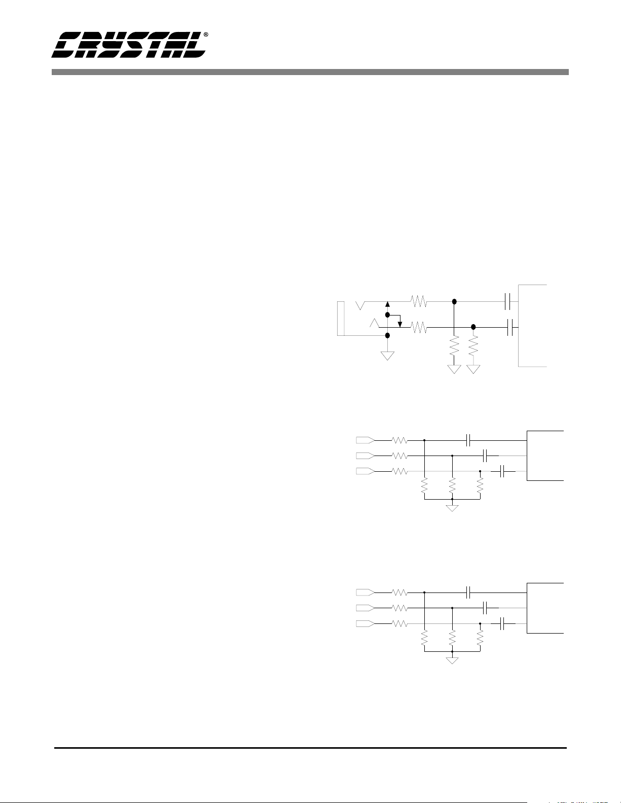
CS4299
6. ANALOG HARDWARE
DESCRIPTION
The analog line-level input hardware consists of
four stereo inputs (LINE_IN_L/R, CD_L/GND/R,
VIDEO_L/R, and AUX_L/R), two selectable
mono microphone inputs (MIC1 and MIC2), and
two mono inputs (PC_BEEP and PHONE). The analog line-level output hardware consists of a mono
output (MONO_OUT), and dual stereo line outputs
(LINE_OUT_L/R and ALT_LINE_OUT_L/R).
This section describes the analog hardware needed
to interface with these pins. The designs presented
in this section comply with specifications detailed
in Chapter 17 of the Microsoft
PC Design Guide-
lines [7] (referred to as PC 99). For EMI reduction
techniques refer to the application note N165:
CS4297A/CS4299 EMI Reduction Techniques [5].
6.1 Analog Inputs
All analog inputs to the CS4299, including
CD_GND, should be capacitively coupled to the
input pins. Unused analog inputs should be tied together and connected through a capacitor to analog
ground or tied to the Vrefout pin directly. The maximum allowed voltage for analog inputs, except the
microphone input, is 1 V
. For the microphone
RMS
input the maximum allowed voltage depends on the
selected boost setting.
6.1.1 Line-Level Inputs
Figure 10 shows circuitry for a line-level stereo input. Replicate this circuit for the Line, Video and
Aux inputs. This design attenuates the input by
6 dB, bringing the signal from the PC 99 specified
2 V
, to the CS4299 maximum allowed 1 V
RMS
RMS
6.1.2 CD Input
connected to the CD analog source ground. Following the reference designs in Figure 11 and
Figure 12 provides extra attenuation of common
mode noise coming from the CD-ROM drive,
thereby producing a higher quality signal. One percent resistors are recommended since closely
matched resistor values provide better common-mode attenuation of unwanted signals. The
circuit shown in Figure 11 can be used to attenuate
a 2 V
CD input signal by 6 dB. The circuit
RMS
shown in Figure 12 can be used for a 1 V
put signal.
Ω
6.8 k
6.8 k
Ω
Ω
6.8 k
Figure 10. Line Input (Replicate for Video and Aux)
6.8 k
CD_R
CD_L
CD_COM
(All resistors 1%)
Figure 11. Differential 2 V
CD_R
.
CD_L
CD_COM
6.8 k
3.4 k
100
100
100
Ω
Ω
Ω
6.8 k
Ω
Ω
Ω
47 k
6.8 k
Ω
AGND
47 k
Ω
1.0 µF
µ
F
1.0
Ω
6.8 k
1.0 µF
1.0 µF
2.2 µF
Ω
3.4 k
Ω
CD Input
RMS
1.0 µF
1.0 µF
2.2 µF
Ω
47 k
Ω
RMS
R
CD in-
L
CD_R
CD_L
CD_GND
CD_R
CD_L
CD_GND
The CD line-level input has an extra pin,
CD_GND, providing a pseudo-differential input
for both CD_L and CD_R. This pin takes the
common-mode noise out of the CD inputs when
36
AGND
Figure 12. Differential 1 V
CD Input
RMS

CS4299
Figure 13. Microphone Input
6.1.3 Microphone Inputs
Figure 13 illustrates an input circuit suitable for dynamic and electret microphones. Electret, or phantom-powered, microphones use the right channel
(ring) of the jack for power. The design also supports the recommended advanced frequency response for voice recognition as specified in PC 99.
Note the microphone input to the CS4299 has an
integrated pre-amplifier. Using the 20dB bit in the
Microphone Volume Register (Index 0Eh) the
pre-amplifier gain can be set to 0 dB or 20 dB.
Figure 14 shows an external pre-amplifier circuit
for an additional 18 dB gain.
2 k
Ω
Vrefout
0.1 µF
1 µF
47 k
220 pF
NPO
+
0.33 µF
X7R
Ω
MIC1
or
MIC2
0.33 µF
47
100 pF
NPO
47 k
Ω
6.8 K
Ω
Ω
+
MC33078 or
MC33178
3.3 µF
6.1.4 PC Beep Input
The PC_BEEP input is useful for mixing the output
of the “beeper” (timer chip), provided in most PCs,
with the other audio signals. When the CS4299 is
held in reset, PC_BEEP is passed directly to the
line output. This allows the system sounds or
“beeps” to be available before the AC ’97 interface
has been activated. Figure 15 illustrates a typical
input circuit for the PC_BEEP input. If PC_BEEP
is driven from a CMOS gate, the 4.7 kΩ resistor
should be tied to analog ground instead of +5VA.
Although this input is described for a low-quality
“beeper”, it is of the same high-quality as all other
analog inputs and may be used for other purposes.
+5VA (Low Noise) or
AGND if CMOS Source
4.7 k
Ω
PC_BEE P
0.1 µF
X7R
PC-BEEP-BUS
47 k
2.7 nF
X7R
Ω
AGND
Figure 15. PC_BEEP Input
+5 VA
+5 VA
U1A
8
MC33078D
3
+
1
2
-
100
+
AGND
4
AGND
k
Ω
10 µF
6.8
47 k
k
Ω
Ω
68
k
Ω
k
Ω
4
3
5
2
1
AGND
2.7
AGND
0.068 µF
X7R
220 pF 220 pF
CGND
AGND
5
6
AGND
+
+5 VA
+
-
220 pF
10 µF
8
7
4
47 k
U1B
MC33078D
Ω
AGND
47
47
X7R
k
Ω
k
Ω
1µF
MIC1/MIC2
Figure 14. Microphone Pre-amplifier
37

CS4299
Figure 16. Modem Connection
6.1.5 Phone Input
One application of the PHONE input is to interface
to the output of a modem analog front end (AFE)
device so that modem dialing signals and protocol
negotiations may be monitored through the audio
system. Figure 16 shows a design for a modem
connection where the output is fed from the
CS4299 MONO_OUT pin through a divider. The
divider ratio shown does not attenuate the signal,
providing an output voltage of 1 V
. If a lower
RMS
output voltage is desired, the resistors can be replaced with appropriate values, as long as the total
load on the output is kept greater than 10 kΩ. The
PHONE input is divided by 6 dB to accommodate
a line-level source of 2 V
RMS
.
6.2 Analog Outputs
The analog line-level output section provides two
stereo outputs and a mono output. The
LINE_OUT_L/R, ALT_LINE_OUT_L/R, and
MONO_OUT pins require 680 pF to 1000 pF NPO
capacitors between the corresponding pin and analog ground. Each analog output is DC-biased up to
the Vrefout signal reference, nominally 2.3 V. This
requires the outputs be AC-coupled to external circuitry (AC load must be greater than 10 kΩ) or DC
coupled to a buffer op-amp biased at Vrefout.
6.2.1 Stereo Outputs
See Figure 18 for a line-level stereo output reference design. See Figure 17 for a recommended
headphone stereo output reference design.
6.2.2 Mono Output
The mono output, MONO_OUT, can be either a
sum of the left and right output channels, attenuated by 6 dB to prevent clipping at full scale, or the
selected Mic signal. The mono out channel can
drive the PC internal mono speaker using an appropriate buffer circuit
PHONE
MONO_OUT
6.8 k
Ω
1.0 µF
0 Ω
6.8 k
Ω
AGND AGND
ALT_LINE_OUT_R
Vrefout
ALT_LINE_OUT_L
Figure 17. Alternate Line Output as Headphone Output
1.0 µF
47 k
Ω
1000 pF
1000 pF
NPO
AGND
PHONE
MONO_OUT
27 k
Ω
27 k
Ω
1000 pF
NPO
39 k
2
-
3
+
TDA1308
5
+
6
-
39 k
Ω
22 pF
NPO
22 pF
NPO
Ω
TDA1308
2
1
3
ALT_LINE_OUT_R
ALT_LINE_OUT_L
VREFOUT
1000 pF
+
220 µF
22 pF
NPO
4
1
2
27 k
Ω
1000 pF
NPO
NPO
AGND
0.1 µF
1 µF
Y5V
AGND
1
3
2
6
5
ELEC
4
3
220 µF
39 k
Ω
ELEC
22 pF
NPO
7
+
TDA1308
10
Ω
+
+
HP_OUT_R
1/4 WATT
Ω
10
HP_OUT_L
1/4 WATT
34
47 k
Ω
1
2
AGND
Figure 18. Stereo Output
220 µF
1
ELEC
+
220
7
µ
ELEC
+
47 k
10 Ω
Watt
1/4
AGND
47 k
1/4
10 Ω
Ω
Watt
F
Ω
Headphone
Out
38

CS4299
6.3 Miscellaneous Analog Signals
The AFLT1 and AFLT2 pins must have a 1000 pF
NPO capacitor to analog ground. These capacitors
provide a single-pole low-pass filter at the inputs to
the ADCs. This makes low-pass filters at each analog input pin unnecessary.
The REFFLT pin must have a 1 µF and a 0.1 µF capacitor connected to analog ground with a short,
wide trace to this pin (see Figure 21 in Section 8,
Grounding and Layout, for an example). The 1 µF
capacitor must not be replaced with any value higher than 1 µF. No other connection should be made,
as any coupling onto this pin will degrade the analog performance of the CS4299. Likewise, digital
signals should be kept away from REFFLT for similar reasons.
The Vrefout pin is typically 2.3 V and provides a
common mode signal for single-supply external
circuits. Vrefout only supports light DC loads and
should be buffered if AC loading is needed. For
typical use the Vrefout pin should have a 1 µF and
a 0.1 µF capacitor connected to analog ground.
6.4 Power Supplies
The power supplies providing analog power should
be as clean as possible to minimize coupling into
the analog section which could degrade analog performance. The analog power pins, AVdd1 and
AVdd2, supply power to all the analog circuitry on
the CS4299. The +5 V analog supply should be
generated from a linear voltage regulator (7805
type) connected to a +12 V supply. This helps isolate the analog circuitry from noise typically found
on +5 V digital supplies. A typical voltage regulator circuit for analog power using a
MC78M05CDT +5 V regulator is shown in
Figure 19. The digital power pins, DVdd1 and
DVdd2, should be connected to the same digital
supply as the controller AC-link interface. The digital interface on the CS4299 may operate at either
+3.3 V or +5 V and proper connection of these pins
will depend on the digital power supply of the controller.
6.5 Reference Design
See Section 11 for a CS4299 reference design.
Y5V
0.1µF
+12VD
MC78M05CDT
1
IN
+
ELEC
10µF
Figure 19. Voltage Regulator
GND
2
OUT
3
Y5V
0.1µF
+5VA
AGNDDGND
+
ELEC
10µF
39

CS4299
7. SONY/PHILIPS DIGITAL INTERFACE (S/PDIF)
The S/PDIF digital output is used to interface the
CS4299 to consumer audio equipment external to
the PC. This output provides an interface for storing digital audio data or playing digital audio data
to digital speakers. Figure 20 illustrates the circuits
necessary for implementing the IEC-958 optical or
consumer interface. For further information on
S/PDIF operation see application note AN22: Over-
view of Digital Audio Interface Data Structures [3].
For further information on S/PDIF recommended
transformers see application note AN134: AES and
S/PDIF Recommended Transformers [4].
8. GROUNDING AND LAYOUT
Figure 21 on page 41 shows the conceptual layout
for the CS4299. The decoupling capacitors should
be located physically as close to the pins as possible. Also note the connection of the REFFLT decoupling capacitors to the ground return trace
connected directly to the ground return pin, AVss1.
cuitry. All analog components and traces should be
located over the analog ground plane and all digital
components and traces should be located over the
digital ground plane.
The common connection point between the two
ground planes (required to maintain a common
ground voltage potential) should be located under
the CS4299. The AC-link digital interface connection traces should be routed such that the digital
ground plane lies underneath these signals (on the
internal ground layer). This applies along the entire
length of these traces from the AC ’97 controller to
the CS4299.
Refer to the Application Note AN18: Layout and
Design Rules for Data Converters and Other
Mixed Signal Devices [2] for more information on
layout and design rules.
It is strongly recommended that separate analog
and digital ground planes be used. Separate ground
planes keep digital noise and return currents from
modulating the CS4299 ground potential and degrading performance. The digital ground pins
should be connected to the digital ground plane and
kept separate from the analog ground connections
of the CS4299 and any other external analog cir-
J1
T
1
SPDO/SDO2
DVdd
3.3V
R
247.5
1
R
107.6
2
S/PDIF_OUT
5V
375
Ω
Ω
Ω
93.75
R
1
R
2
DGND
Ω
Figure 20. S/PDIF Output
+5V_PCI
0.1µF
DGND
SPDO/SDO2
8.2 k
Ω
4
3
2
1
TOTX-173
5
DGND
6
DGND
40
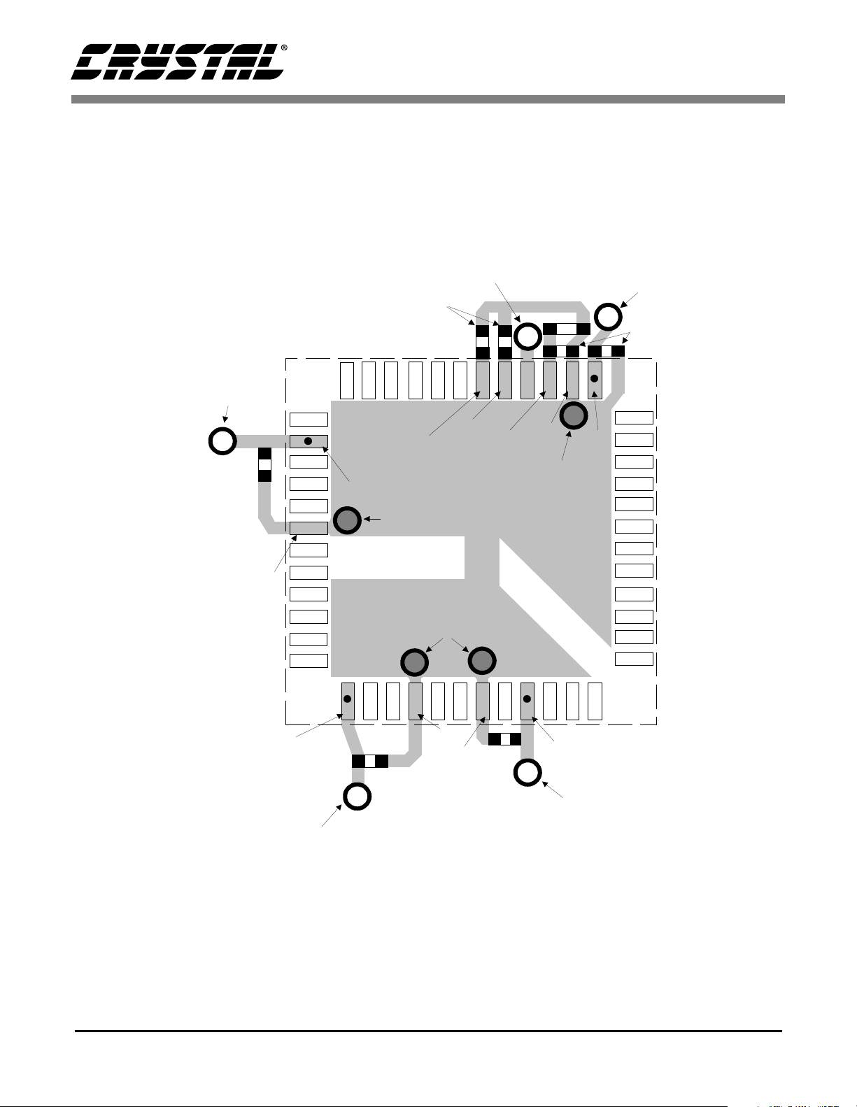
CS4299
Via to +5VA
0.1 µF
Y5V
AVss2
AVdd2
1000 pF
NPO
AFLT2
Via to Analog
Ground
Digital
Ground
Via to Digital Ground
Vrefout
to via
AFLT1
REFFLT
1
AVss1
Via to Analog
Ground
Analog
Ground
µF
Via to +5VA
0.1 µF
Y5V
AVdd1
Pin 1
DVdd1
Via to +5VD or +3.3VD
0.1 µF
Y5V
DVss1
DVss2
0.1 µF
Y5V
Figure 21. Conceptual Layout for the CS4299
DVdd2
Via to +5VD or +3.3VD
41

9. PIN DESCRIPTIONS
2
ALT_LINE_OUT_L
d
d
V
A
s2
s
ID1#
EAPD
S/PDIF_OUT
48 47 46 45 44 43 42 41 40 39 38 37
ID0#
NC
NC
AV
C
N
ALT_LINE_OUT_R
T
U
O
_
O
N
MO
CS4299
DVdd1
XTL_IN
XTL_OUT
DVss1
SDATA_OUT
BIT_CLK
DVss2
SDATA_IN
DVdd2
SYNC
RESET#
PC_BEEP
1
2
3
CS4299-xQ
(48-Pin TQFP)
4
5
6
7
8
9
10
11
12
13 14 15 16 17 18 19 20 21 22 23 24
L
E
_
X
AU
PHON
Figure 22. Pin Locations for the CS4299
R
_
X
AU
L
O_
E
D
I
V
R
O_
E
D
I
V
L
D
_
D
C
CD_GN
R
CD_
1
C
I
M
2
C
I
M
L
_
N
I
_
NE
I
L
36
35
34
33
32
31
30
29
28
27
26
25
R
_
N
I
_
NE
I
L
LINE_OUT_R
L
INE_O
UT_L
FLTO
FLTI
FLT3D
BPCFG
AFLT2
AFLT1
Vrefout
REFFLT
AVss1
AVdd1
42

Audio I/O
PC_BEEP - Analog Mono Source, Input, Pin 12
The PC_BEEP input is intended to allow the PC system POST (Power On Self-Test) tones to pass
through to the audio subsystem. The PC_BEEP input has two connections: the first connection is to the
analog output mixer, the second connection is directly to the LINE_OUT stereo outputs. While the
RESET# pin is actively being asserted and the BCFG pin is left floating, the PC_BEEP bypass path to
the LINE_OUT outputs is enabled. While the CS4299 is in normal operation mode, with RESET#
deasserted or BCFG grounded, PC_BEEP is a monophonic source to the analog output mixer. The
maximum allowable input is 1 V
reference and requires AC-coupling to external circuitry. If this input is not used, it should be connected
to the Vrefout pin or AC-coupled to analog ground.
PHONE - Analog Mono Source, Input, Pin 13
This analog input is a monophonic source to the analog output mixer. It is intended to be used as a
modem subsystem input to the audio subsystem. The maximum allowable input is 1 V
This input is internally biased at the Vrefout voltage reference and requires AC-coupling to external
circuitry. If this input is not used, it should be connected to the Vrefout pin or AC-coupled to analog
ground.
MIC1 - Analog Mono Source, Input, Pin 21
(sinusoidal). This input is internally biased at the Vrefout voltage
RMS
CS4299
(sinusoidal).
RMS
This analog input is a monophonic source to the analog output mixer. It is intended to be used as a
desktop microphone connection to the audio subsystem. The CS4299 internal mixer’s microphone input
is MUX selectable with either MIC1 or MIC2 as the input. The maximum allowable input is 1 V
(sinusoidal). This input is internally biased at the Vrefout voltage reference and requires AC-coupling to
external circuitry. If this input is not used, it should be connected to the Vrefout pin or AC-coupled to
analog ground.
MIC2 - Analog Mono Source, Input, Pin 22
This analog input is a monophonic source to the analog output mixer. It is intended to be used as an
alternate microphone connection to the audio subsystem. The CS4299 internal mixer’s microphone input
is MUX selectable with either MIC1 or MIC2 as the input. The maximum allowable input is 1 V
(sinusoidal). This input is internally biased at the Vrefout voltage reference and requires AC-coupling to
external circuitry. If this input is not used, it should be connected to the Vrefout pin or AC-coupled to
analog ground.
LINE_IN_L, LINE_IN_R - Analog Line Source, Inputs, Pins 23 and 24
These inputs form a stereo input pair to the CS4299. The maximum allowable input is 1 V
(sinusoidal). These inputs are internally biased at the Vrefout voltage reference and require AC-coupling
to external circuitry. If these inputs are not used, they should both be connected to the Vrefout pin or
both AC-coupled, with separate AC-coupling caps, to analog ground.
CD_L, CD_R - Analog CD Source, Inputs, Pins 18 and 20
These inputs form a stereo input pair to the CS4299. It is intended to be used for the Red Book CD
audio connection to the audio subsystem. The maximum allowable input is 1 V
inputs are internally biased at the Vrefout voltage reference and require AC-coupling to external circuitry.
If these inputs are not used, they should both be connected to the Vrefout pin or both AC-coupled, with
separate AC-coupling caps, to analog ground.
(sinusoidal). These
RMS
RMS
RMS
RMS
CD_GND - Analog CD Common Source, Input, Pin 19
This analog input is used to remove common mode noise from Red Book CD audio signals. The
impedance on the input signal path should be one half the impedance on the CD_L and CD_R input
paths. This pin requires AC-coupling to external circuitry. If this input is not used, it should be connected
to the Vrefout pin or AC-coupled to analog ground.
43

VIDEO_L, VIDEO_R - Analog Video Audio Source, Inputs, Pins 16 and 17
These inputs form a stereo input pair to the CS4299. It is intended to be used for the audio signal
output of a video device. The maximum allowable input is 1 V
internally biased at the Vrefout voltage reference and require AC-coupling to external circuitry. If these
inputs are not used, they should both be connected to the Vrefout pin or both AC-coupled, with separate
AC-coupling caps, to analog ground.
AUX_L, AUX_R - Analog Auxiliary Source, Inputs, Pins 14 and 15
CS4299
(sinusoidal). These inputs are
RMS
These inputs form a stereo input pair to the CS4299. The maximum allowable input is 1 V
(sinusoidal). These inputs are internally biased at the Vrefout voltage reference and require AC-coupling
to external circuitry. If these inputs are not used, they should both be connected to the Vrefout pin or
both AC-coupled, with separate AC-coupling caps, to analog ground.
LINE_OUT_L, LINE_OUT_R - Analog Line-Level, Outputs, Pins 35 and 36
These signals are analog outputs from the stereo output mixer. The full-scale output voltage for each
output is nominally 1 V
(sinusoidal). These outputs are internally biased at the Vrefout voltage
RMS
reference and require either AC-coupling to external circuitry or DC-coupling to a buffer op-amp biased
at the Vrefout voltage. These pins need a 680-1000 pF NPO capacitor attached to analog ground.
ALT_LINE_OUT_L, ALT _LINE_OUT_R - Analog Alternate Line-Level, Outputs, Pins 39 and 41
These signals are analog outputs from the stereo output mixer. The full-scale output voltage for each
output is nominally 1 V
(sinusoidal). These outputs are internally biased at the Vrefout voltage
RMS
reference and require either AC-coupling to external circuitry or DC-coupling to a buffer op-amp biased
at the Vrefout voltage. These pins need a 680-1000 pF NPO capacitor attached to analog ground.
MONO_OUT - Analog Mono Line-Level, Output, Pin 37
This signal is an analog output from the stereo-to-mono mixer or MIC1/2. The full-scale output voltage
for this output is nominally 1 V
(sinusoidal). This output is internally biased at the Vrefout voltage
RMS
reference and requires either AC-coupling to external circuitry or DC-coupling to a buffer op-amp biased
at the Vrefout voltage. This pin needs a 680-1000 pF NPO capacitor attached to analog ground.
RMS
Clock and Configuration
XTL_IN - Crystal Input/Clock Input, Pin 2
In primary mode this pin requires either a 24.576 MHz crystal, with the other pin attached to XTL_OUT,
or an external CMOS clock. The crystal frequency must be 24.576 MHz and designed for fundamental
mode, parallel resonance operation. If an external CMOS clock is used to drive this pin, it must run at
24.576 MHz. In secondary mode all timing is derived from the BIT_CLK input signal and this pin should
be left floating.
XTL_OUT - Crystal Output, Pin 3
This pin is used when a crystal is placed between XTL_OUT and XLT_IN. If an external 24.576 MHz
clock is used on XTL_IN, this pin must be left floating with no traces or components connected to it. In
secondary mode this pin should be left floating.
ID1#, ID0# - Codec ID, Inputs, Pins 45 and 46
These pins select the Codec ID and mode of operation for the CS4299. They are only sampled after the
rising edge of RESET#. These pins are internally pulled up to the digital supply voltage and should be
left floating for logic ‘0’ or tied to digital ground for logic ‘1’. When both pins are left floating the CS4299
is the primary codec. If either or both pins are tied to ground the CS4299 is a secondary codec.
44

Analog Reference, Filters, and Configuration
REFFLT - Internal Reference Voltage, Input, Pin 27
This signal is the voltage reference used internal to the CS4299. A 0.1 µF and a 1.0 µF (must not be
larger than 1 µF) capacitor with short, wide traces must be connected to this pin. No other connections
should be made to this pin.
Vrefout - Voltage Reference, Output, Pin 28
All analog inputs and outputs are centered around Vrefout, nominally 2.3 Volts. This pin may be used to
level shift external circuitry. This pin cannot drive any DC loads, thus any external loading must be
buffered.
AFLT1 - Left ADC Channel Antialiasing Filter, Input, Pin 29
This pin needs a 1000 pF NPO capacitor connected to analog ground.
AFLT2 - Right ADC Channel Antialiasing Filter, Input, Pin 30
This pin needs a 1000 pF NPO capacitor connected to analog ground.
FLTI, FLTO - 3D Filter, Input, Pin 33 and 34
A 1000 pF capacitor must be connected between FLTI and FLTO if the 3D function is used.
FLT3D - 3D Filter, Input, Pin 32
A 0.01 µF capacitor must be connected from this pin to AGND if the 3D function is used.
BCFG - Beep Configuration, Input, Pin 31
This pin is the configuration control for the PC_BEEP bypass path. If this pin is grounded, the bypass
path is disabled. If this pin is left floating, the PC_BEEP bypass path is enabled.
CS4299
Misc. Digital Interfaces
S/PDIF_OUT - Sony/Philips Digital Interface, Output, Pin 48
This pin generates the S/PDIF digital output from the CS4299 when the SPEN bit in the S/PDIF Control
Register (Index 68h) is ‘set’. This output may be used to directly drive a resistive divider and coupling
transformer to an RCA-type connector for use with consumer audio equipment.
EAPD - External Amplifier Powerdown, Output, Pin 47
This pin is used to control the powerdown state of an audio amplifier external to the CS4299. The
output is controlled by the EAPD bit in the Powerdown Ctrl/Stat Register (Index 26h). It is driven as a
normal CMOS output and defaults low (‘0’) upon power-up.
45

AC-Link
RESET# - AC ’97 Chip Reset, Input, Pin 11
This active low signal is the asynchronous Cold Reset input to the CS4299. The CS4299 must be reset
before it can enter normal operating mode.
SYNC - AC-Link Serial Port Sync pulse, Input, Pin 10
This signal is the serial port timing signal for the AC-link. Its period is the reciprocal of the maximum
sample rate, 48 kHz. The signal is generated by the controller, synchronous to BIT_CLK. SYNC is an
asynchronous input when the CS4299 is configured as a primary audio codec and is in a PR4
powerdown state. A series terminating resistor of 47 Ω should be connected on the signal near the
SYNC source.
BIT_CLK - AC-Link Serial Port Master Clock, Input/Output, Pin 6
This input/output signal controls the master clock timing for the AC-link. In primary mode, this signal is a
12.288 MHz output clock derived from a 24.576 MHz crystal on the XTL_IN input clock. When the
CS4299 is in secondary mode, this signal is an input which controls the AC-link serial interface and
generates all internal clocking including the AC-link serial interface timing and the analog sampling
clocks. A series terminating resistor of 47 Ω should be connected on this signal close to the CS4299 in
primary mode or close to the BIT_CLK source in secondary mode.
CS4299
SDATA_OUT - AC-Link Serial Data Input Stream to AC ’97, Input, Pin 5
This input signal receives the control information and digital audio output streams. The data is clocked
into the CS4299 on the falling edge of BIT_CLK. A series terminating resistor of 47 Ω should be
connected on this signal near the controller.
SDATA_IN - AC-Link Serial Data Output Stream from AC ’97, Output, Pin 8
This output signal transmits the status information and digital audio input streams from the ADCs. The
data is clocked out of the CS4299 on the rising edge of BIT_CLK. A series terminating resistor of 47 Ω
should be connected on this signal as close to the CS4299 as possible.
Power Supplies
DVdd1, DVdd2 - Digital Supply Voltage, Pins 1 and 9
Digital supply voltage for the AC-link section of the CS4299. These pins can be tied to +5 V digital or to
+3.3 V digital. The CS4299 and controller AC-link should share a common digital supply
DVss1, DVss2 - Digital Ground, Pins 4 and 7
Digital ground connection for the AC-link section of the CS4299. These pins should be isolated from
analog ground currents.
AVdd1, AVdd2 - Analog Supply Voltage, Pins 25 and 38
Analog supply voltage for the analog and mixed signal sections of the CS4299. These pins must be tied
to the analog +5 V power supply. It is strongly recommended that +5 V be generated from a voltage
regulator to ensure proper supply currents and noise immunity from the rest of the system.
AVss1, AVss2 - Analog Ground, Pins 26 and 42
Ground connection for the analog, mixed signal, and substrate sections of the CS4299. These pins
should be isolated from digital ground currents.
46

10. PARAMETER AND TERM DEFINITIONS
AC ’97 Specification
Refers to the Audio Codec ’97 Component Specification Ver 2.1 published by the Intel
AC ’97 Controller or Controller
Refers to the control chip which interfaces to the audio codec AC-link. This has been also called DC ’97
for Digital Controller ’97 [6].
AC ’97 Registers or Codec Registers
Refers to the 64-field register map defined in the AC ’97 Specification.
ADC
Refers to a single Analog-to-Digital converter in the CS4299. “ADCs” refers to the stereo pair of
Analog-to-Digital converters. The CS4299 ADCs have 18-bit resolution.
Codec
Refers to the chip containing the ADCs, DACs, and analog mixer. In this data sheet, the codec is the
CS4299.
DAC
CS4299
®
Corporation [6].
Refers to a single Digital-to-Analog converter in the CS4299. “DACs” refers to the stereo pair of
Digital-to-Analog converters. The CS4299 DACs have 20-bit resolution.
dB FS A
dB FS is defined as dB relative to full-scale. The “A” indicates an A weighting filter was used.
Differential Nonlinearity
The worst case deviation from the ideal code width. Units in LSB.
Dynamic Range (DR)
DR is the ratio of the RMS full-scale signal level divided by the RMS sum of the noise floor, in the
presence of a signal, available at any instant in time (no change in gain settings between
measurements). Measured over a 20 Hz to 20 kHz bandwidth with units in dB FS A.
FFT
Fast Fourier Transform.
Frequency Response (FR)
FR is the deviation in signal level verses frequency. The 0 dB reference point is 1 kHz. The amplitude
corner, Ac, lists the maximum deviation in amplitude above and below the 1 kHz reference point. The
listed minimum and maximum frequencies are guaranteed to be within the Ac from minimum frequency
to maximum frequency inclusive.
Fs
Sampling Frequency.
Interchannel Gain Mismatch
For the ADCs, the difference in input voltage to get an equal code on both channels. For the DACs, the
difference in output voltages for each channel when both channels are fed the same code. Units are in
dB.
47

Interchannel Isolation
The amount of 1 kHz signal present on the output of the grounded AC-coupled line input channel with 1
kHz, 0 dB, signal present on the other line input channel. Units are in dB.
Line-level
Refers to a consumer equipment compatible, voltage driven interface. The term implies a low driver
impedance and a minimum 10
Paths
A-D: Analog in, through the ADCs, onto the serial link.
D-A: Serial interface inputs through the DACs to the analog output.
A-A: Analog in to Analog out (analog mixer).
PC 99
CS4299
kΩ load impedance.
Refers to the PC 99 System Design Guide published by the Microsoft
PLL
Phase Lock Loop. Circuitry for generating a desired clock from an external clock source.
Resolution
The number of bits in the output words to the DACs, and in the input words to the ADCs.
Signal to Noise Ratio (SNR)
SNR, similar to DR, is the ratio of an arbitrary sinusoidal input signal to the RMS sum of the noise floor,
in the presence of a signal. It is measured over a 20 Hz to 20 kHz bandwidth with units in dB.
S/PDIF
Sony/Phillips Digital Interface. This interface was established as a means of digitally interconnecting
consumer audio equipment. The documentation for S/PDIF has been superseded by the IEC-958
consumer digital interface document.
SRC
Sample Rate Converter. Converts data derived at one sample rate to a differing sample rate. The
CS4299 operates at a fixed sample frequency of 48 kHz. The internal sample rate converters are used
to convert digital audio streams playing back at other frequencies to 48 kHz.
®
Corporation [7].
Total Harmonic Distortion plus Noise (THD+N)
THD+N is the ratio of the RMS sum of all non-fundamental frequency components, divided by the RMS
full-scale signal level. It is tested using a -3 dB FS input signal and is measured over a 20 Hz to 20 kHz
bandwidth with units in dB FS.
48

11. REFERENCE DESIGN
CS4299
J4
43521
LINE OUT
ELEC
+
C15 10uF
ABITCLK
ASDIN
ASYNC
ASDOUT
ARST#
AC LINK
PCI Audio Controller
or ICH Controller
C11
0.1uF
X7R
C10
0.1uF
X7R
+5VA+12V
U1 MC 78M05ACDT
C6
10uF
ELEC
+
C5
0.1uF
X7R
3
OUT
GND
2
IN
1
C4
C3
+
+3.3VD
C9
0.1uF
X7R
AGND
0.1uF
X7R
10uF
ELEC
U3
C8
0.1uF
X7R
AGND
R8 47
11
36
35
10
8
6
5
AVdd2
38
AVdd1
BIT_CLK
25
AVss2
42
AVss1
26
DVdd2
9
DVdd1
1
DVss1
DVss2
4
7
SDATA_IN
SDATA_OUT
CS4299
DGND
41
SYNC
RESET#
LINE_OUT_R
LINE_OUT_L
PC_BEEP
AUX_L14AUX_R
12
15
20
PHONO-1/8
R13
R12
ELEC
+
C17 10uF
39
31
37
MONO_OUT
ALT_LINE_OUT_L
ALT_LINE_OUT_R
CD_L18CD_GND19CD_R
MIC121MIC222LINE_IN_L23LINE_IN_R
24
AGND
220K
220K
J6
TOTX-173
12345
C18
NPO
1000pF
AGNDAGND AGND AGND
C19
NPO
1000pF
48
44
40
45
nc7
BCFG
EAPD47ID1#46ID0#
17
nc643nc5
S/PDIF_OUT
XTL_OUT
3
XTL_IN
2
FLTO
34
FLTI
33
REFFLT27Vrefout28AFLT129AFLT2
FLT3D
32
30
PHONE
VIDEO_L16VIDEO_R
13
S/PDIF OUT
C29
NPO
1000pF
C28
0.01uF
X7R
C27
NPO
1000pF
C26
NPO
1000pF
C25
0.1uF
X7R
C24
1uF
Y5V
6
DGNDDGND
R21
6.8K
C31
0.1uF
X7R
+5VD
Y1
C34
22pF
NPO
DGND
(50 PPM)
24.576 MHz
C33
22pF
NPO
DGNDAGND
Figure 23. CS4299 Reference Design
X7R
C1 0. 1uF
C2
2700pF
X7R
R2
6.8K
R1 47K
1
2
J1
PC SPEAKER
IN
C23
0.1uF
X7R
60 mil trace
GND_TIE
DGND AGND
Tie at one point only
C22
1uF
Y5V
R19 1.5K
R18 2.2K
43521
J7
MIC IN
1uF
R20 100
1uF
Y5V
1uF
Y5V
C7
AGND
R3 6.8K
AGND
DGND
2X1HDR-SN/PB
AUX IN
C12
R4 6.8K
J2
R6 6.8K
R5 6.8K
123
4
1uF
Y5V R7 47
1uF
Y5V
1uF
Y5V
C13
C14
C16
R10 100K
R9 100K
AGND
AGND
4
4X1HDR-AU
J3
CD IN
R11 100K
123
4X1HDR-AU
1uF
Y5V
C20
R14 6.8K
AGND
43521
J5
LINE IN
1uF
Y5V
C21
R16 6.8K
R15 6.8K
R17 6.8K
PHONO-1/8
+5VA
AGND AGND
under the codec
Y5V
C30
C32
10uF
ELEC
+
PHONO-1/8
AGND
AGND
49

12. REFERENCES
1) Cirrus Logic, Audio Quality Measurement Specification, Version 1.0, 1997
http://www.cirrus.com/products/papers/meas/meas.html
CS4299
2) Cirrus Logic, AN18: Layout and Design Rules for Data Converters and Other Mixed Signal Devices
Version 6.0, February 1998
3) Cirrus Logic, AN22: Overview of Digital Audio Interface Data Structures
, Version 2.0, February 1998
4) Cirrus Logic, AN134: AES and S/PDIF Recommended Transformers, Version 2, April 1999
5) Cirrus Logic, AN165: CS4297A/CS4299 EMI Reduction Techniques
6) Intel
®
, Audio Codec ’97 Component Specification, Revision 2.1, May 1998
, Version 1.0, September 1999
http://developer.intel.com/ial/scalableplatforms/audio/index.htm
7) Microsoft®, PC 99 System Design Guide, Version 1.0, July 1999
http://www.microsoft.com/hwdev/desguid/
®
8) Intel
82801AA (ICH) and 82801AB (ICH0) I/O Controller Hub, June 1999
http://developer.intel.com/design/chipsets/datashts/290655.htm
,
50

13. PACKAGE DIMENSIONS
48L LQFP PACKAGE DRAWING
D1
D
CS4299
E
E1
1
e
∝
B
A
A1
L
INCHES MILLIMETERS
DIM MIN NOM MAX MIN NOM MAX
A --- 0.055 0.063 --- 1.40 1.60
A1 0.002 0.004 0.006 0.05 0.10 0.15
B 0.007 0.009 0.011 0.17 0.22 0.27
D 0.343 0.354 0.366 8.70 9.0 BSC 9.30
D1 0.272 0.28 0.280 6.90 7.0 BSC 7.10
E 0.343 0.354 0.366 8.70 9.0 BSC 9.30
E1 0.272 0.28 0.280 6.90 7.0 BSC 7.10
e* 0.016 0.020 0.024 0.40 0.50 BSC 0.60
L 0.018 0.24 0.030 0.45 0.60 0.75
∝
* Nominal pin pitch is 0.50 mm
0.000° 4° 7.000° 0.00° 4° 7.00°
Controlling dimension is mm.
JEDEC Designation: MS022
51

 Loading...