

Page 1
CS4223
CS4224
24-Bit 105 dB Audio Codec with Volume Control
Features
105 dB Dynamic Range A/D Converters
105 dB Dynamic Range D/A Converters
110 dB DAC Signal-to-Noise Ratio (EIAJ)
Analog Volume Control (CS4224 only)
Differential Inputs / Outputs
On-chip Anti-aliasing and Output Smoothing
Filters
De-emphasis for 32, 44.1 and 48 kHz
Supports Master and Slave Modes
Single +5 V power supply
On-Chip Crystal Oscillator
3-5VDigitalInterface
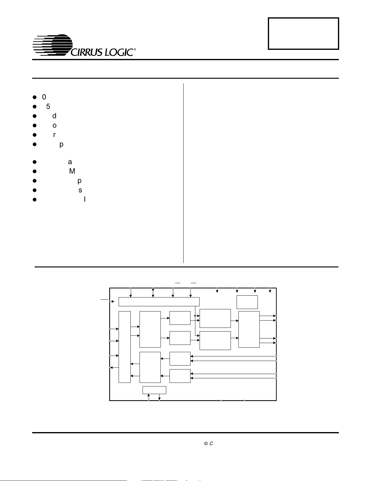
I
Description
The CS4223/4 is a highly integrated, high performance,
24-bit, audio codec providing stereo analog-to-digital and
stereo digital-to-analog converters using delta-sigma
conversion techniques. The device operates from a single +5 V power supply, and features low power
consumption. Selectable de-emphasis filter for 32, 44.1,
and 48 kHz sample rates is also included.
The CS4224 includes an analog volume control capable
of 113.5 dB attenuation in 0.5 dB steps. The analog volume control architecture preserves dynamic range
during attenuation. Volume control changes are implemented using a “soft” ramping or zero crossing
technique.
Applications include digital effects processors, DAT, and
multitrack recorders.
ORDERING INFORMATION
CS4223-KS -10 to +70 °C 28-pin SSOP
CS4223-BS -40 to +85 °C 28-pin SSOP
CS4223-DS -40 to +85 °C 28-pin SSOP
CS4224-KS -10 to +70 °C 28-pin SSOP
CDB4223/4 Evaluation Board
Cirrus Logic, Inc.
http://www.cirrus.com
RST
LRCK
SCLK
SDIN
SDOUT
(
)(
DIF1
SCL/CCLK SDA/CDIN AD0/CS MCLK VD VA
Serial Audio Data I nterface
)(
DIF0
Cont rol Port
Digital Filters
with De-Emphasis
Digital Filters
Clock OSC
XTI XTO
)
(
DEM0
Left
DAC
Right
DAC
Left
ADC
Right
ADC
( ) = CS4223
)
DEM1
2
IC/SPI
CopyrightCirrus Logic, Inc. 2002
V
L
Volume
Cont rol
Volume
Cont rol
DGND AGND
= CS4224
*
(All Rights Reserved)
*
*
Voltag e
Reference
Analog Low Pass
and Output St age
AOUTL+
AOUTL-
AOUTR+
AOUTR-
AINLAINL+
AINRAINR+
JAN ‘03
DS290F1
1
Page 2

TABLE OF CONTENTS
1. CHARACTERISTICS AND SPECIFICATIONS ........................................................................ 4
SPECIFIED OPERATING CONDITIONS ................................................................................. 4
ABSOLUTE MAXIMUM RATINGS ........................................................................................... 4
ANALOG CHARACTERISTICS ................................................................................................ 5
SWITCHING CHARACTERISTICS .......................................................................................... 8
SWITCHING CHARACTERISTICS - CONTROL PORT - SPI MODE (CS4224) ..................... 9
SWITCHING CHARACTERISTICS - CONTROL PORT - I
2. TYPICAL CONNECTION DIAGRAM — CS4223 ...................................................................11
3. TYPICAL CONNECTION DIAGRAM — CS4224 ...................................................................12
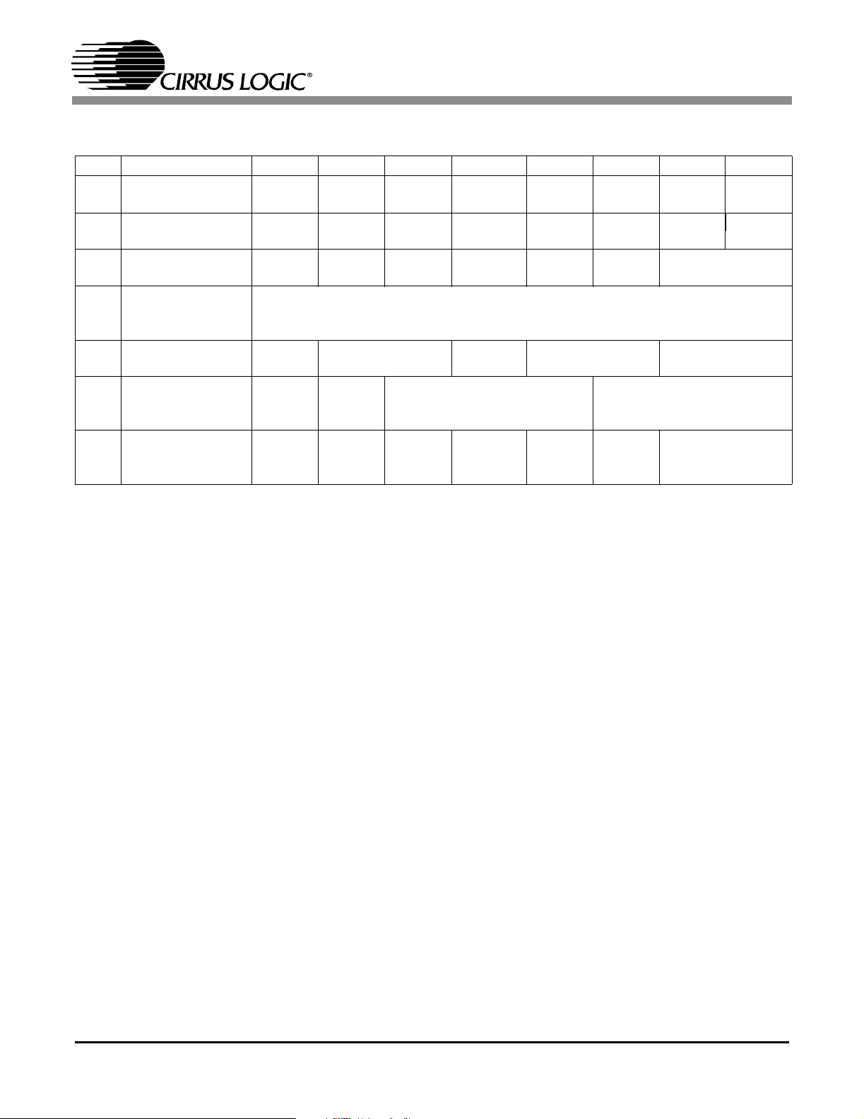
4. REGISTER QUICK REFERENCE - CS4224 .......................................................................... 13
5. REGISTER DESCRIPTIONS - CS4224 .................................................................................. 14
5.1 ADC Control (address 01h)............................................................................................... 14
5.1.1 Power Down ADC (PDN)............................................................................................... 14
5.1.2 Left and Right channel High Pass Filter Defeat (HPDR-HPDL)..................................... 14
5.1.3 Left and Right Channel ADC Muting (ADMR-ADML)..................................................... 14
5.1.4 Calibration Control (CAL)...............................................................................................14
5.1.5 Calibration Status (CALP) (Read Only) ......................................................................... 14
5.1.6 Clocking Error (CLKE) (Read Only) ............................................................................... 15
5.2 DAC Control (address 02h)............................................................................................... 15
5.2.1 Mute on Consecutive Zeros (MUTC) ............................................................................. 15
5.2.2 Mute Control (MUTR-MUTL).......................................................................................... 15
5.2.3 Soft RAMP Control (SOFT)............................................................................................ 15
5.2.4 Soft RAMP Step Rate (RMP).........................................................................................16
5.3 Left Channel Output Attenuator Level (address 03h) ....................................................... 16
5.4 Right Channel Output Attenuator Level (address 04h) ....................................................16
5.4.1 Attenuation level (ATT7-ATT0) ...................................................................................... 16
5.5 DSP Port Mode (address 05h) .......................................................................................... 17
5.5.1 De-emphasis Control (DEM).......................................................................................... 17
5.5.2 Serial Input/Output Data SCLK Polarity Select (DSCK)................................................. 17
CS4223 CS4224
2
C MODE (CS4224) .................... 10
Contacting Cirrus Logic Support
For a complete listing of Direct Sales, Distributor, and Sales Representative contacts, visit the Cirrus Logic web site at:
http://www.cirrus.com/corporate/contacts/sales.cfm
IMPORTANT NOTICE
"Preliminary" product information describes products that are in product ion, but for which full charact erization data is not yet available. "Advance" product information describes products that are in development and subject to development changes. Cirrus Logic, Inc. and its subsidiaries ("Cirrus") bel ieve that the information
contained in this document is accurate and r eliable. However, the information is subject to change without notice and is provided "AS IS" wi thout warranty of any
kind (express or i mplied). Customers are advised to obtain the latest version of relevant informati on to verify, before placing orders, that informati on being rel ied
on is current and complete. All products are sold subject to the terms and conditions of sale supplied at the time of order acknowledgment, including those pertaining
to warranty, patent infringement, and limitation of l iability. No responsibility is assumed by Cirrus for the use of this informati on, including use of this information as
the basis for manufactur e or sale of any items, or for infringement of patents or other rights of third parties. This document is the property of Cirr us and by furnishing
this information, Cirrus grants no license, express or implied under any patents, mask work rights, copyrights, trademarks, trade secrets or other intel lectual property
rights. Cirrus owns the copyrights of the information contained herein and gives consent for copies to be made of the information only for use within your organization
with respect to Cirrus integrated circuits or other parts of Cirrus. This consent does not extend to other copying such as copying for gener al distribution, advertising
or promotional purposes, or for creating any work for resale.
An export permit needs to be obtained from the competent authorities of the Japanese Government if any of the products or technologies descri bed in thismaterial
and controlled under the "Foreign Exchange and Foreign Trade Law" is to be exported or taken out of Japan. An export license and/or quota needs to be obtained
from the competent authorities of t he Chinese Government if any of the products or technologies described in thi s material is subj ect to t he PRC Foreign Trade Law
and is to be exported or taken out of the PRC.
CERTAIN APPLICATIONS USING SEMICONDUCTOR PRODUCTS MAY INVOLVE POTENTIAL RISKS OF DEATH, PERSONAL INJURY, OR SEVERE PROPERTY OR ENVIRONMENTAL DAMAGE ( "CRITICAL APPLICATIONS"). CIRRUS PRODUCTS ARE NOT DESI GNED, AUTHORIZED, OR WARRANTED TO BE
SUITABLE FOR USE IN LIFE-SUPPORT DEVICES OR SYSTEMS OR OTHER CRITICAL APPLICATIONS. INCLUSION OF CIRRUS PRODUCTS IN SUCH
APPLICATIONS IS UNDERSTOOD TO BE FULLY AT THE CUSTOMER'S RI SK.
Purchase of I
those components in a standard I
Cirrus Logic, Cirrus, and the Cirrus Logi c logo designs are trademarks of Cirrus Logic, Inc. All other brand and product names i n this document may be trademarks
or servi ce marks of their respective owners.
2 DS290F1
2
C components of Cirrus Logic, Inc., or one of its sublicensed Associated Companies conveys a license under the Philli ps I2C Patent Rights to use
2
Csystem.
Page 3

CS4223 CS4224
5.5.3 Serial Data Output Format (DOF).................................................................................. 17
5.5.4 Serial Data Input Format (DIF) ...................................................................................... 17
5.6 Converter Status Report (Read Only) (address 06h) ....................................................... 18
5.6.1 Left and Right Channel Acceptance Bit (ACCR-ACCL) ................................................ 18
5.6.2 Left and Right Channel ADC Output Level (LVR and LVL) ........................................... 18
5.7 Master Clock Control (address 07h)................................................................................. 18
5.7.1 Master Clock Control (MCK).......................................................................................... 18
6. PIN DESCRIPTIONS — CS4223 ............................................................................................ 19
7. PIN DESCRIPTIONS — CS4224 ............................................................................................ 21
8. APPLICATIONS ..................................................................................................................... 23
8.1 Overview .......................................................................................................................... 23
8.2 Grounding and Power Supply Decoupling ....................................................................... 23
8.3 High Pass Filter ...............................................................................................................23
8.4 Analog Outputs ................................................................................................................23
8.5 Master vs. Slave Mode .................................................................................................... 23
8.6 De-emphasis ................................................................................................................... 23
8.7 Power-up / Reset / Power Down Calibration ................................................................... 23
8.8 Control Port Interface (CS4224 only) .............................................................................. 24
8.8.1 SPI Mode ............................................................................................................ 24
2
8.8.2 I
8.9 Memory Address Pointer (MAP)....................................................................................... 25
8.9.1 Auto-Increment Control (INCR) ..................................................................................... 25
8.9.2 Register Pointer (MAP).................................................................................................. 25
9. ADC/DAC FILTER RESPONSE.............................................................................................. 29
10. PARAMETER DEFINITIONS................................................................................................. 30
11. PACKAGE DIMENSIONS ..................................................................................................... 31
C Mode ............................................................................................................. 24
LIST OF FIGURES
Figure 1. Serial Audio Port Data I/O Timing ............................................................................ 8
Figure 2. SPI Control Port Timing............................................................................................ 9
Figure 3. I
Figure 4. CS4223 Recommended Connection Diagram ....................................................... 11
Figure 5. CS4224 Recommended Connection Diagram ....................................................... 12
Figure 6. Control Port Timing, SPI mode............................................................................... 25
Figure 7. Control Port Timing, I
Figure 8. Serial Audio Format 0 (I2S).................................................................................... 26
Figure 9. Serial Audio Format 1............................................................................................. 26
Figure 10. Serial Audio Format 2............................................................................................. 26
Figure 11. Serial Audio Format 3............................................................................................. 27
Figure 12. Optional Input Buffer .............................................................................................. 27
Figure 13. Single-ended Input Application............................................................................... 27
Figure 14. 2- and 3-Pole Butterworth Filters............................................................................ 28
Figure 15. De-emphasis Curve................................................................................................ 28
Figure 16. Hybrid Analog/Digital Attenuation........................................................................... 28
Figure 17. ADC Filter Response.............................................................................................. 29
Figure 18. ADC Passband Ripple............................................................................................ 29
Figure 19. ADC Transition Band.............................................................................................. 29
Figure 20. DAC Filter Response.............................................................................................. 29
Figure 21. DAC Passband Ripple............................................................................................ 29
Figure 22. DAC Transition Band.............................................................................................. 29
2
C Control Port Timing .......................................................................................... 10
2
C mode ............................................................................... 25
DS290F1 3
Page 4

LIST OF TABLES
Table 1. Example Volume Settings ...............................................................................................16
Table 2. Common Clock Frequencies ........................................................................................... 19
Table 3. Digital Interface Format - DIF1 and DIF0 .......................................................................20
Table 4. De-emphasis Control.......................................................................................................20
Table 5. Common Clock Frequencies ........................................................................................... 21
CS4223 CS4224
4 DS290F1
Page 5
CS4223 CS4224
1. CHARACTERISTICS AND SPECIFICATIONS
(All Min/Max characteristics and specifications are guaranteed over the Specified Operating Conditions. Typical
performance characteristics and specifications are derived from measurements taken at nominal supply voltages
and T
SPECIFIED OPERATING CONDITIONS
(AGND, DGND = 0 V, all voltages with respect to 0 V.)
Power Supplies Digital
Ambient Operating Temperature Commercial (-KS)
ABSOLUTE MAXIMUM RATINGS (AGND, DGND = 0 V, all voltages with respect to 0 V.)
Power Supplies Digital
Input Current (Note 1) - ±10 mA
Analog Input Voltage (Note 2) -0.7 VA + 0.7 V
Digital Input Voltage (Note 2) -0.7 VD + 0.7 V
Ambient Temperature Power Applied -55 +125 °C
Storage Temperature -65 +150 °C
=25°C.)
A
Parameter Symbol Min Nom Max Unit
VD
Analog
Digital
|VA-VD|
Industrial (-BS/-DS)
Parameter Symbol Min Max Unit
Analog
VA
VL
T
T
VD
VA
AC
AI
4.75
4.75
2.7
-
-10
-40
-0.3
-0.3
5.0
5.0
5.0
-
-
-
6.0
6.0
5.25
5.25
5.25
0.4
70
85
V
V
V
V
°C
°C
V
V
WARNING: Operation at or beyond these limits may result in permanent damage to the device.
Normal operation is not guaranteed at these extremes.
Notes: 1. Any pin except supplies. Transient currents of up to 100 mA on the analog input pins will not cause SCR
latch-up.
2. The maximum over or under voltage is limited by the input current.
DS290F1 5
Page 6
CS4223 CS4224
ANALOG CHARACTERISTICS (Full Scale Input Sine wave, 997 Hz; Fs = 48 kHz; Measurement
Bandwidth is 20 Hz to 20 kHz; Local components as shown in Figures 4 and 5.)
CS4223/4 - KS CS4223/4 - BS/ - DS
Parameter Symbol
Analog Input Characteristics
Total Harmonic Distortion THD - 0.0014 - - 0.0014 - %
Dynamic Range A-weighted
unweighted
Total Harmonic Distortion + Noise (Note 3) THD+N - -97 -90 - -97 -87 dB
Interchannel Isolation (1 kHz) - 90 - - 90 - dB
Interchannel Gain Mismatch - - 0.1 - - 0.1 dB
Offset Error with High Pass Filter - - 0 - - 0 LSB
Full Scale Input Voltage (Differential) 1.9 2.0 2.1 1.9 2.0 2.1 Vrms
Gain Drift - 100 - - 100 - ppm/°C
Input Resistance 10 - - 10 - - kΩ
Input Capacitance - - 15 - - 15 pF
Common Mode Input Voltage - 2.3 - - 2.3 - V
Common Mode Rejection Ratio CMRR 75 - - 75 - - dB
A/D Decimation Filter Characteristics
Passband (Note 4) 0 - 21.8 0 - 21.8 kHz
Passband Ripple - - ±0.01 - - ±0.01 dB
Stopband (Note 4) 30 - 6114 30 - 6114 kHz
Stopband Attenuation (Note 5) 80 - - 80 - - dB
Group Delay (Fs = Output Sample Rate) Left
(Note 6) Right
Group Delay Variation vs. Frequency ∆t
High Pass Filter Characteristics
Frequency Response -3 dB (Note 4)
-0.1 dB
Phase Deviation @ 20 Hz (Note 4) - 10 - - 10 - Degree
Passband Ripple - - 0 - - 0 dB
t
gd_L
t
gd_R
gd
98
95
105
102
-
18/Fs
-
17/Fs
--0--0µs
-
-
3.7
20
-
-
-
-
-
-
95
92
105
102
-
18/Fs
-
17/Fs
-
-
3.7
20
UnitMin Typ Max Min Typ Max
-
-
-
-
-
-
dB
dB
s
s
Hz
Hz
Notes: 3. Referenced to typical full-scale differential input voltage (2 Vrms).
4. Filter characteristics scale with output sample rate. For output sample rates, Fs, other than 48 kHz, the
0.01 dB passband edge is 0.4535x Fs and the stopband edge is 0.625x Fs.
5. The analog modulator samples the input at 6.144 MHz for an Fs equal to 48 kHz. There is no rejection
of input signals which are multiples of the sampling frequency (n x 6.144 MHz ±21.8 kHz where
n = 0,1,2,3...).
6. Group delay for Fs = 48 kHz, t
6 DS290F1
= 18/48 kHz = 375 µs.
gd
Page 7
CS4223 CS4224
ANALOG CHARACTERISTICS (CONTINUED)
CS4223/4 - KS CS4223/4 - BS/ - DS
Parameter Symbol
Analog Output Characteristics - Minimum Attenuation, 10 kΩ, 100 pF load; unless otherwise specified.
Signal-to-Noise, Idle-Channel Noise
(CS4224 only) DAC muted, A-weighted
Dynamic Range DAC not muted, A-weighted
DAC not muted, unweighted
Total Harmonic Distortion THD - 0.0014 - - 0.0014 - %
Total Harmonic Distortion + Noise THD+N - -97 -92 - -97 -87 dB
Interchannel Isolation (1 kHz) - 90 - - 90 - dB
Interchannel Gain Mismatch - - 0.1 - - 0.1 dB
Attenuation Step Size All Outputs 0.35 0.5 0.65 0.35 0.5 0.65 dB
Programmable Output Attenuation Span 110 113.5 - 110 113.5 - dB
Differential Offset Voltage - ±10 - - ±10 - mV
Common Mode Output Voltage - 2.4 - - 2.4 - V
Full Scale Output Voltage 1.8 1.9 2.0 1.8 1.9 2.0 Vrms
Gain Drift - 100 - - 100 - ppm/°
Out-of-Band Energy Fs/2 to 2 Fs - -60 - - -60 - dBFs
Analog Output Load Resistance
Capacitance
Combined Digital and Analog Filter Characteristics
Frequency Response10 Hz to 20 kHz - ±0.1 - - ±0.1 - dB
Deviation from Linear Phase - ±0.5 - - ±0.5 - Degree
Passband: to 0.01 dB corner (Notes 7 and 8) 0 - 21.8 0 - 21.8 kHz
Passband Ripple (Note 8) - - ±0.01 - - ±0.01 dB
Stopband (Notes 7 and 8) 26.2 - - 26.2 - - kHz
Stopband Attenuation (Note 9) 70 - - 70 - - dB
Group Delay (Fs = Input Sample Rate) Left
Right
Power Supply
Power Supply Current VA
Total Power Down
Power Supply Rejection Ratio 1 kHz - 65 - - 65 - dB
VD
VL
t
gd_L
t
gd_R
102 110 - 97 110 - dB
10097105
102
10
-
-
-
-
-
-
-
-
-
26/Fs
27/Fs
46
9
3
0.4
-
-
-
100
-
-
60
20
5
-
95
92
10
105
102
-
-
-
-
-
-
-
-
-
26/Fs
27/Fs
46
9
3
0.4
100
60
20
UnitMin Typ Max Min Typ Max
-
-
-
-
-
5
-
dB
dB
C
kΩ
pF
s
s
mA
mA
mA
mA
Notes: 7. The passband and stopband edges scale with frequency. For input word rates, Fs, other than 48 kHz,
the 0.01 dB passband edge is 0.4535x Fs and the stopband edge is 0.5465x Fs.
8. Digital filter characteristics.
9. Measurement bandwidth is 10 Hz to 3 Fs.
DS290F1 7
Page 8
CS4223 CS4224
DIGITAL CHARACTERISTICS
Parameter Symbol Min Max Unit
High-level Input Voltage VL = 5V
VL = 3V
Low-level Input Voltage V
High-level Output Voltage at I
Low-level Output Voltage at I
=-2.0mA V
O
=2.0mA V
O
V
IH
V
IH
IL
OH
OL
2.8
2.0
-0.3 0.8 V
VL - 1.0 - V
-0.5V
Input Leakage Current Digital Inputs - 10 µA
Output Leakage Current High Impedance Digital Outputs - 10 µA
VL + 0.3
VL + 0.3
V
V
8 DS290F1
Page 9
CS4223 CS4224
SWITCHING CHARACTERISTICS (Outputs loaded with 30 pF)
Parameter Symbol Min Typ Max Unit
Audio ADC’s and DAC’s Sample Rate Fs 4 - 50 kHz
XTI Frequency XTI = 256, 384, or 512 Fs 1.024 - 26 MHz
XTI Pulse Width High XTI = 512 Fs
XTI = 384 Fs
XTI = 256 Fs
XTI Pulse Width Low XTI = 512 Fs
XTI = 384 Fs
XTI = 256 Fs
XTI Jitter Tolerance - 500 - psRMS
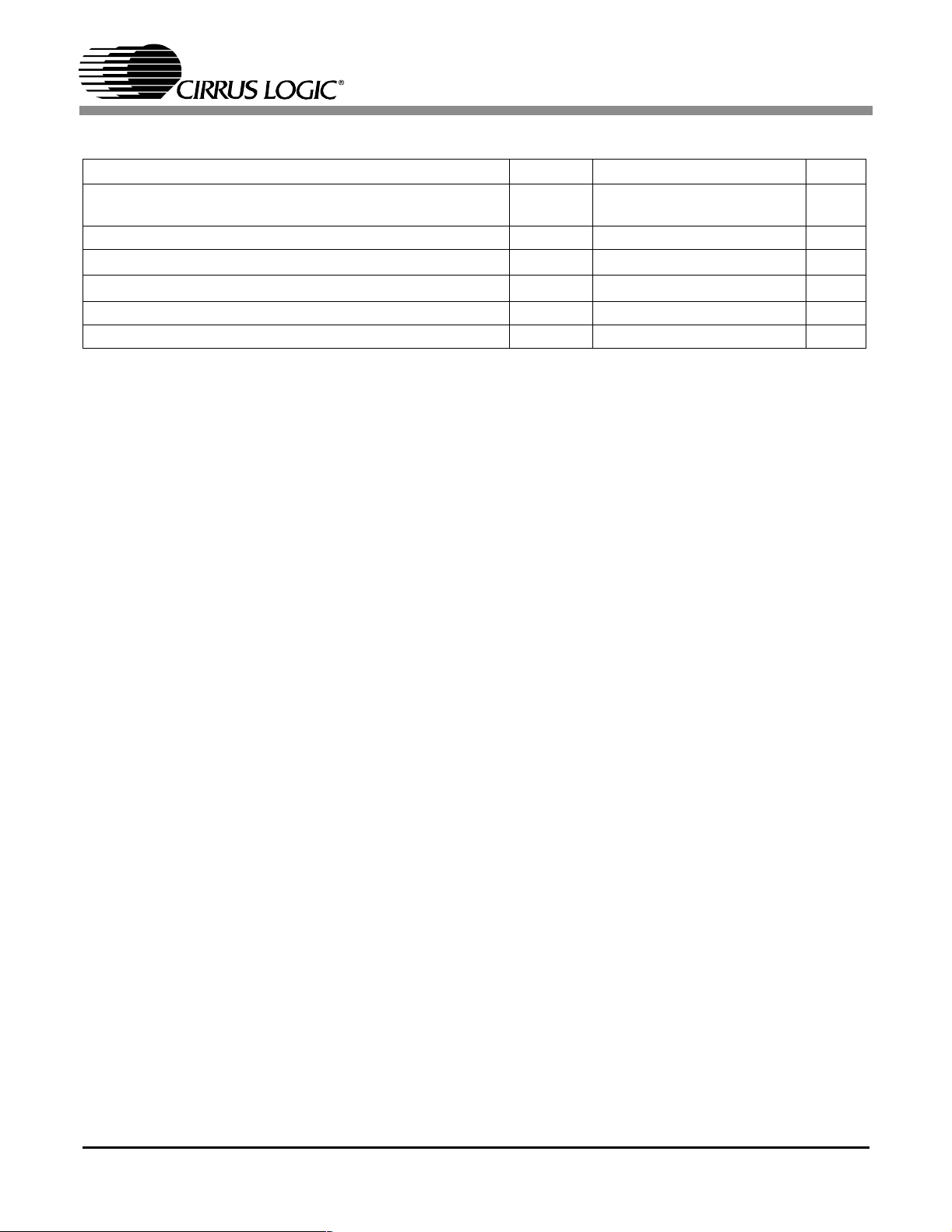
Low Time (Note 10) 10 - - ms
RST
SCLK falling edge to SDOUT output valid DSCK = 0 t
LRCK edge to MSB valid t
SDIN setup time before SCLK rising edge DSCK = 0 t
SDIN hold time after SCLK rising edge DSCK = 0 t
SCLK Period t
SCLK High Time t
SCLK Low Time t
SCLK rising to LRCK edge DSCK = 0 t
LRCK edge to SCLK rising DSCK = 0 t
dpd
lrpd
ds
dh
sckw
sckh
sckl
lrckd
lrcks
13
21
31
13
21
31
-- ns
-
-
-
-
-
-
-
-
-
-
-
-
1
---------------------- 2 0+
(384) Fs
ns
ns
ns
ns
ns
ns
--45ns
25 - - ns
25 - - ns
1
---------------------(128) Fs
--ns
40 - - ns
40 - - ns
35 - - ns
40 - - ns
Notes: 10. After powering up the CS4223/4, PDN should be held low for 10 ms to allow the power supply to settle.
LRCK
t
lrckd
SCLK*
SDIN
SDOUT
*SCLK shown for DSCK = 0, SCLK inverted for DSCK = 1.
t
lrpd
t
lrcks
t
ds
t
sckh
t
dh
MSB MSB-1
t
sckw
t
sckl
t
dpd
Figure 1. Serial Audio Port Data I/O Timing
DS290F1 9
Page 10
CS4223 CS4224
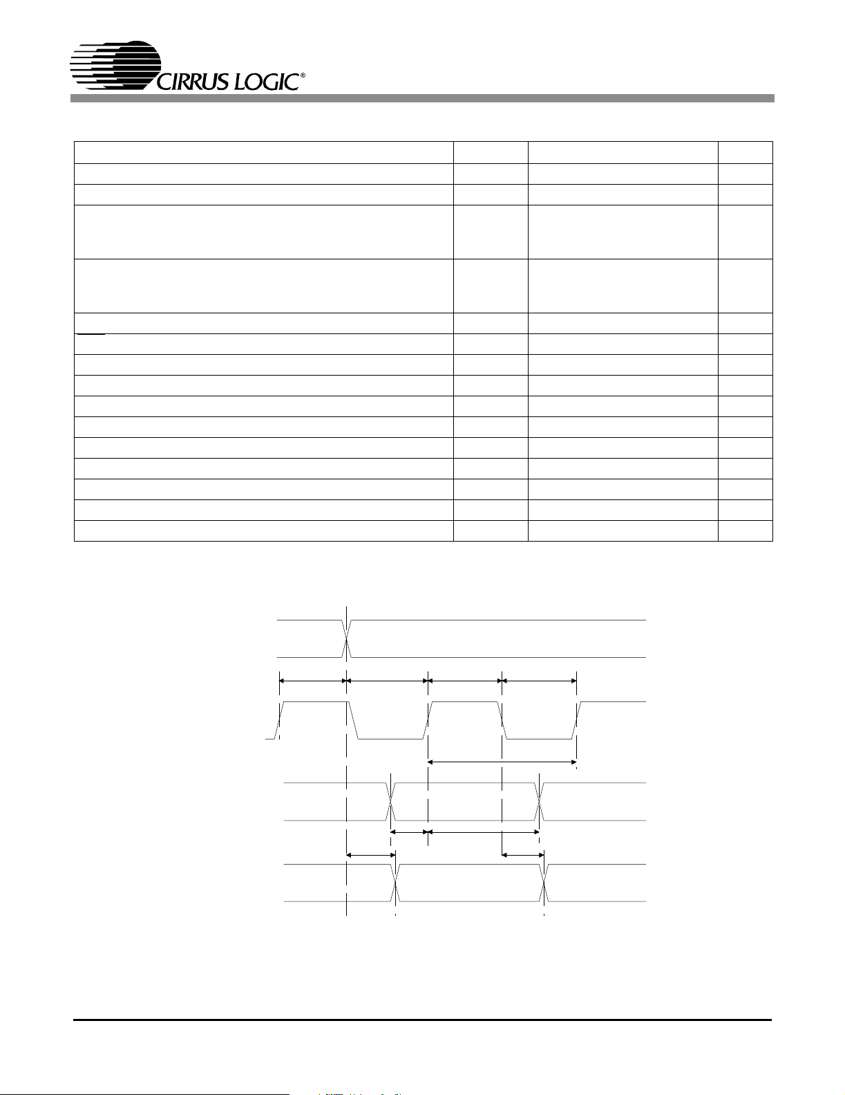
SWITCHING CHARACTERISTICS - CONTROL PORT - SPI MODE (CS4224)
(Inputs: Logic 0 = DGND, Logic 1 = VD; CL=30pF)
Parameter Symbol Min Max Unit
SPI Mode (SPI
/I2C = 0)
CCLK Clock Frequency f
RST
rising edge to CS falling (Note 11) t
CCLK edge to CS
High Time between transmissions t
CS
CS
falling to CCLK edge t
falling (Note 12) t
CCLK Low Time t
CCLK High Time t
CDIN to CCLK rising setup time t
CCLKrisingtoDATAholdtime (Note13) t
Rise time of CCLK and CDIN (Note 14) t
Fall time of CCLK and CDIN (Note 14) t
Notes: 11. Not tested but guaranteed by design.
12. t
only needed before first falling edge of CS after RST rising edge. t
spi
13. Data must be held for sufficient time to bridge the transition time of CCLK.
14. For F
SCK
<1MHz.
sck
srs
spi
csh
css
scl
sch
dsu
dh
r2
f2
-6MHz
41 - µs
500 - ns
1.0 - µs
20 - ns
66 - ns
66 - ns
40 - ns
15 - ns
- 100 ns
- 100 ns
= 0 at all other times.
spi
RST
CS
CCLK
CDIN
t
srs
t
t
css
spi
t
r2
Figure 2. SPI Control Port Timing
t
t
scl
t
t
f2
dsu
sch
t
dh
t
csh
10 DS290F1
Page 11
CS4223 CS4224
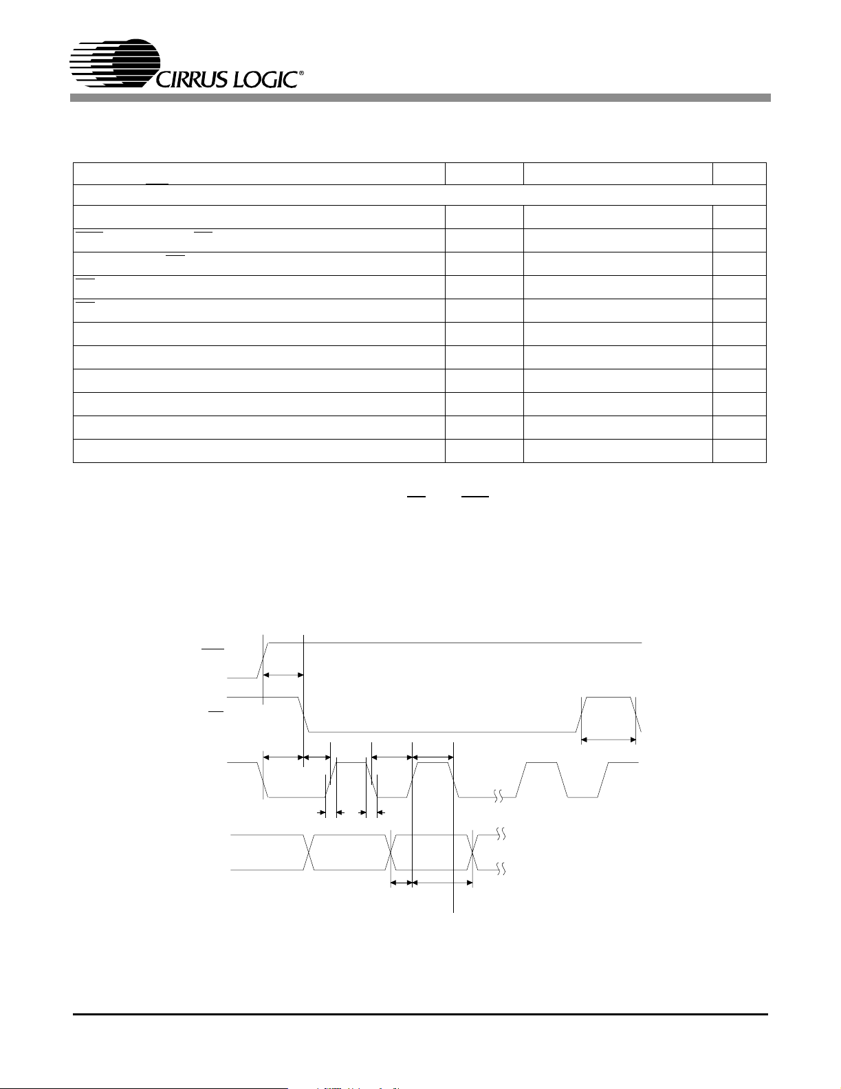
SWITCHING CHARACTERISTICS - CONTROL PORT - I2C MODE (CS4224)
(Inputs: Logic 0 = DGND, Logic 1 = VD; CL=30pF)
Parameter Symbol Min Max Unit
2C®
Mode (SPI/I2C = 1)
I
SCL Clock Frequency f
RST
rising edge to Start (Note 15)
Bus Free Time between transmissions t
Start Condition Hold Time (prior to first clock pulse) t
Clock Low Time t
Clock High Time t
Setup time for repeated Start Condition t
SDAholdtimeforSCLfalling (Note16) t
SDA setup time to SCL rising t
Rise time of SCL t
Fall time of SCL t
Rise time of SDA t
Fall time of SDA t
Setup time for Stop Condition t
scl
t
irs
buf
hdst
low
high
sust
hdd
sud
rc
fc
rd
fd
susp
- 100 kHz
50 - µs
4.7 - µs
4.0 - µs
4.7 - µs
4.0 - µs
4.7 - µs
0-µs
250 - ns
-25ns
-25ns
-1µs
- 300 ns
4.7 - µs
Notes: 15. Not tested but guaranteed by design.
16. Data must be held for sufficient time to bridge the 300 ns transition time of SCL.
RST
t
irs
Stop Start
SDA
SCL
t
buf
t
t
hdst
low
t
hdd
t
high
t
sud
Repeated
Start
t
sust
t
hdst
t
rd
t
fc
t
rc
Stop
t
fd
t
susp
Figure 3. I2C Control Port Timing
DS290F1 11
Page 12

2. TYPICAL CONNECTION DIAGRAM — CS4223
CS4223 CS4224
+5V
Supply
Ferrite Bead
+ 0.1 µF
150
150
150
150
Mode Selection
1µF
Ω
Ω
Ω
Ω
20
2.2 nF
19
17
2.2 nF
16
10
11
27
21 6
VA VD
AINL+
AINL-
AINR+
AINR-
DIF1
DIF0
RST
CS4223
2
Ω
VL
AOUTL+
AOUTL-
AOUTR+
AOUTR-
DEM1
DEM0
XTI
XTO
0.1 µF + 1µF
13
25
26
Analog Filter
24
23
18
12
3
2
Analog Filter
Digital Audio
40 pF
0.1 µF + 1µF
Source
40 pF
Eliminate the crystal
and capacitors when
using an external
clock input
+2.7 - 5V
External
Clock Input
R
*
47 k
s
R
s
R
s
R
s
Audio
DSP
Ω
R=500
s
Ω
* Required for
Master Mode only
1
NC
14
NC
15
NC
28
NC
AGND
22
Figure 4. CS4223 Recommended Connection Diagram
SCLK
LRCK
SDIN
SDOUT
DGND
7
5
4
9
8
(Also see Recommended Layout Diagram)
12 DS290F1
Page 13

3. TYPICAL CONNECTION DIAGRAM — CS4224
CS4223 CS4224
+5V
Supply
Ferrite Bead
Microcontroller
R = 500
s
* Required for
Master Mode only
Ω
+ 0.1 µF
1µF
Ω
150
150
150
150
Ω
Ω
Ω
20
2.2 nF
19
17
2.2 nF
16
10
11
12
27
18
1
14
15
28
Ω
2
21 6
VA VD
AINL+
AINL-
AINR+
CS4224
AINR-
SCL/CCLK
SDA/CDIN
AD0/CS
RST
I2C/SPI
NC
NC
NC
NC
AGND DGND
22 7
VL
AOUTL+
AOUTL-
AOUTR+
AOUTR-
XTI
XTO
SCLK
LRCK
SDIN
SDOUT
0.1 µF + 1µF
13
25
26
24
23
3
2
5
4
9
8
Analog Filter
Analog Filter
40 pF
R
R
R
R
*
Ω
47 k
s
s
s
s
0.1 µF + 1µF
External
40 pF
Eliminate the crystal
and capacitors when
using an external
clock input
Audio
DSP
Clock Input
+2.7 - 5V
Figure 5. CS4224 Recommended Connection Diagram
(Also see Recommended Layout Diagram)
DS290F1 13
Page 14
CS4223 CS4224
4. REGISTER QUICK REFERENCE - CS4224
Addr Function 7 6 5 4 3 2 1 0
0h Reserved Reserved Reserved Reserved Reserved Reserved Reserved Reserved Reserved
default 0 0 0 0 0 0 0 0
1h ADC Control PDN HPDR HPDL ADMR ADML CAL CALP CLKE
default 0 0 0 0 0 0 0 0
2h DAC Control Reserved MUTC MUTR MUTL SOFT Reserved RMP1 RMP0
default 0 0 0 0 0 0 0 0
3h-4h Output Attenuator
Level
default 0 0 0 0 0 0 0 0
5h DSP Port Mode Reserved DEM1 DEM0 DSCK DOF1 DOF0 DIF1 DIF0
default 0 0 0 0 0 0 0 0
6h Converter Status
Report
default 0 0 0 0 0 0 0 0
7h Master Clock
Control
default 0 0 0 0 0 0 0 0
ATT7 ATT6 ATT5 ATT4 ATT3 ATT2 ATT1 ATT0
ACCR ACCL LVR2 LVR1 LVR0 LVL2 LVL1 LVL0
Reserved Reserved Reserved Reserved Reserved Reserved MCK1 MCK0
14 DS290F1
Page 15

CS4223 CS4224
5. REGISTER DESCRIPTIONS - CS4224
Note: All registers are read/write in I2C mode and write-only in SPI mode, unless otherwise noted.
5.1 ADC Control (address 01h)
76543210
PDN HPDR HPDL ADMR ADML CAL CALP CLKE
00000000
5.1.1 POWER DOWN ADC (PDN)
Default = 0
0 - Disabled
1-Enabled
Function:
The ADC will enter a low-power state when this function is enabled.
5.1.2 LEFT AND RIGHT CHANNEL HIGH PASS FILTER DEFEAT (HPDR-HPDL)
Default = 0
0 - Disabled
1-Enabled
Function:
The internal high-pass filter is defeated when this function is enabled. Control of the internal highpass filter is independent for the left and right channel.
5.1.3 LEFT AND RIGHT CHANNEL ADC MUTING (ADMR-ADML)
Default = 0
0 - Disabled
1-Enabled
Function:
The output for the selected ADC channel will be muted when this function is enabled.
5.1.4 CALIBRATION CONTROL (CAL)
Default = 0
0 - Disabled
1-Enabled
Function:
The device will automatically perform an offset calibration when brought out of reset, which last approximately 50 ms. When this function is enabled, a rising edge on the reset line will initiate an offset
calibration.
5.1.5 CALIBRATION STATUS (CALP) (READ ONLY)
Default = 0
0 - Calibration done
1 - Calibration in progress
DS290F1 15
Page 16

CS4223 CS4224
5.1.6 CLOCKING ERROR (CLKE) (READ ONLY)
Default = 0
0 - No error
1 - Error
5.2 DAC Control (address 02h)
76543210
Reserved MUTC MUTR MUTL SOFT Reserved RMP1 RMP0
00000000
5.2.1 MUTE ON CONSECUTIVE ZEROS (MUTC)
Default = 0
0 - Disabled
1-Enabled
Function:
The DAC output will mute following the reception of 512 consecutive audio samples of static 0 or -1
when this function is enabled. A single sample of non-static data will release the mute. Detection and
muting is done independently for each channel. The muting function is affected, similar to volume
control changes, by the SOFT bit in the DAC Control register.
5.2.2 MUTE CONTROL (MUTR-MUTL)
Default = 0
0 - Disabled
1-Enabled
Function:
The output for the selected DAC channel will be muted when this function is enabled. The muting
function is affected, similar to volume control changes, by the SOFT bit in the DAC Control register.
5.2.3 SOFT RAMP CONTROL (SOFT)
Default = 0
0 - Soft Ramp level changes
1 - Zero Cross level changes
Function:
Soft Ramp level changes will be implemented by incrementally ramping, in 0.5 dB steps, from the current level to the new level. The rate of change defaults to 0.5 dB per 8 left/right clock periods and is
adjustable through the RMP bits in the DAC Control register.
Zero Cross level changes will be implemented in a single step from the current level to the new level.
The level change takes effect on a zero crossing to minimize audible artifacts. If the signal does not
encounter a zero crossing, the level change will occur after a timeout period of 512 sample periods
(10.7 ms at 48 kHz sample rate). Zero crossing is independently monitored and implemented for each
channel. The ACCR and ACCL bits in the Converter Status Report register indicate when a level
change has occurred for the right and left channel.
16 DS290F1
Page 17

CS4223 CS4224
5.2.4 SOFT RAMP STEP RATE (RMP)
Default = 00
00 - 1 step per 8 LRCK's
01 - 1 step per 4 LRCK's
10 - 1 step per 16 LRCK's
11 - 1 step per 32 LRCK's
Function:
The rate of change for the Soft Ramp function is adjustable through the RMP bits.
5.3 Left Channel Output Attenuator Level (address 03h)
5.4 Right Channel Output Attenuator Level (address 04h)
76543210
ATT7 ATT6 ATT5 ATT4 ATT3 ATT2 ATT1 ATT0
00000000
5.4.1 ATTENUATION LEVEL (ATT7-ATT0)
Default = 00h
Function:
The Output Attenuator Level registers allow for attenuation of the DAC outputs in 0.5 dB increments
from 0 to 113.5 dB. Level changes are implemented with an analog volume control until the residual
output noise is equal to the noise floor in the mute state. At this point, volume changes are performed
digitally. This technique is superior to purely digital volume control because the noise is attenuated
by the same amount as the signal, thus preserving dynamic range, see Figure 16. Volume changes
are performed as dictated by the SOFT bit in the DAC Control register. ATT0 represents 0.5 dB of
attenuation and settings greater than 227 (decimal value) will mute the selected DAC output.
Binary Code Decimal Value Volume Setting
00000000 00 dB
11100011 227 -113.5 dB
11100100 228 Muted
Table 1. Example Volume Settings
DS290F1 17
Page 18

CS4223 CS4224
5.5 DSP Port Mode (address 05h)
76543210
Reserved
00000000
5.5.1 DE-EMPHASIS CONTROL (DEM)
Function:
5.5.2 SERIAL INPUT/OUTPUT DATA SCLK POLARITY SELECT (DSCK)
DEM1 DEM0 DSCK DOF1 DOF0 DIF1 DIF0
Default = 00
00 - 44.1 kHz de-emphasis setting
01 - 48 kHz de-emphasis setting
10 - 32 kHz de-emphasis setting
11 - De-emphasis disabled
Selects the appropriate digital filter to maintain the standard 15 µs/50 µs digital de-emphasis filter response at 32, 44.1 or 48 kHz sample rates, see Figure 15.
Default = 0
0 - Data valid on rising edge of SCLK
1 - Data valid on falling edge of SCLK
Function:
This function selects the polarity of the SCLK edge used to clock data in and out of the serial audio
port.
5.5.3 SERIAL DATA OUTPUT FORMAT (DOF)
Default = 00
2
00 - I
S compatible
01 - Left justified
10 - Right justified, 24-bit
11 - Right justified, 20-bit
Function:
The required relationship between the left/right clock, serial clock and output serial data is defined by
the Serial Data Output Format, and the options are detailed in Figures 8-11.
Note: If the format selected is Right-Justified, SCLK must be 64 Fs when operating in slave mode.
5.5.4 SERIAL DATA INPUT FORMAT (DIF)
Default = 00
2
00 - I
S compatible
01 - Left justified
10 - Right justified, 24-bit
11- Right justified, 20-bit
Function:
The required relationship between the left/right clock, serial clock and input serial data is defined by
the Serial Data Input Format, and the options are detailed in Figures 8-11.
18 DS290F1
Page 19

CS4223 CS4224
5.6 Converter Status Report (Read Only) (address 06h)
76543210
ACCR ACCL LVR2 LVR1 LVR0 LVL2 LVL2 LVL0
00000000
5.6.1 LEFT AND RIGHT CHANNEL ACCEPTANCE BIT (ACCR-ACCL)
Default = 0
0 - Requested setting valid
1 - New setting loaded
Function:
The ACCR and ACCL bits indicate when a change in the Output Attenuator Level has occurred for
the left and right channels, respectively. The value will be high when a new setting is loaded into the
Output Attenuator Level registers. The value will return low when the requested attenuation setting
has taken effect.
5.6.2 LEFT AND RIGHT CHANNEL ADC OUTPUT LEVEL (LVR AND LVL)
Default = 000
000 - Normal output levels
001 - -6 dB level
010 - -5 dB level
011 - -4 dB level
100 - -3 dB level
101 - -2 dB level
110 - -1 dB level
111 - Clipping
Function:
The analog-to-digital converter is continually monitoring the peak digital signal output for both the left
and right channel, prior to the digital limiter. The maximum output value is stored in the LVL and LVR
bits. The LVL and LVR bits are ‘sticky’, so they are reset after each read is performed.
5.7 Master Clock Control (address 07h)
76543210
Reserved Reserved Reserved Reserved Reserved Reserved MCK1 MCK0
00000000
5.7.1 MASTER CLOCK CONTROL (MCK)
Default = 00
00 - XTI = 256 Fs for Master Mode
01 - XTI = 384 Fs for Master Mode
10 - XTI = 512 Fs for Master Mode
Function:
The MCK bits allow for control of the Master Clock, XTI, input frequency.
Note: These bits are not valid when operating in slave mode.
DS290F1 19
Page 20

6. PIN DESCRIPTIONS — CS4223
NC
XTO
XTI
LRCK
SCLK
VD
DGND
SDOUT
SDIN
DIF1
DIF0
VL
CS4223
1
2
3
4
5
6
7
821
9
10
11
12 17
13
14 15
28
27
26
25
24
23
22
20
19
18
16
NC
RST
AOUTL-
AOUTL+
AOUTR+
AOUTR-
AGND
VA
AINL+
AINL-
DEM1
AINR+DEM0
AINR-
NCNC
CS4223 CS4224
NC 1,14,15, 28 No Connect - These pins are not connected internally and should be tied to DGND to mini-
mize noise coupling.
XTI, XTO 2,3 Crystal Connections (Input/Output)-Input and output connections for the crystal used to
clock the CS4223. Alternatively, a clock may be input into XTI. This is the clock source for the
delta-sigma modulator and digital filters. The frequency of this clock must be either 256x, 384x,
or 512x Fs in Slave Mode and 256x in Master Mode.
Fs (kHz) XTI (MHz)
256x 384x 512x
32 8.1920 12.2880 16.3840
44.1 11.2896 16.9344 22.5792
48 12.2880 18.4320 24.5760
Table 2. Common Clock Frequencies
LRCK 4 Left/Right Clock (Input)-Determines which channel is currently being input/output of the
serial audio data pins SDIN/SDOUT. The frequency of the Left/Right clock must be equal to the
input sample rate. Although the outputs for each ADC channel are transmitted at different
times, Left/Right pairs represent simultaneously sampled analog inputs. The required relationship between the left/right clock, serial clock and serial data is defined by the DIF1-0 pins. The
options are detailed in Figures 8 - 11.
SCLK 5 Serial Data Clock (Input)-Clocks the individual bits of the serial data into the SDIN pin and
out of the SDOUT pin. The required relationship between the left/right clock, serial clock and
serial data is defined by the DIF1-0 pins. The options are detailed in Figures 8 - 11.
VD 6 Digital Power (Input)-Positive power supply for the digital section. Typically 5.0 VDC.
DGND 7 Digital Ground (Input)-Digital ground for the digital section.
SDOUT 8 Serial Data Output (Output)-Two's complement MSB-first serial data is output on this pin.
The required relationship between the left/right clock, serial clock and serial data is defined by
the DIF1-0 pins. The options are detailed in Figures 8 - 11.
20 DS290F1
Page 21

CS4223 CS4224
SDIN 9 Serial Data Input (Input)-Two's complement MSB-first serial data is input on this pin. The
required relationship between the left/right clock, serial clock and serial data is defined by the
DIF1-0 pins. The options are detailed in Figures 8 - 11.
DIF0, DIF1 10,11 Digital Interface Format (Input)-The required relationship between the left/right clock, serial
clock and serial data is defined by the Digital Interface Format. The options are detailed in Figures 8 - 11.
DIF1 DIF0 DESCRIPTION FORMAT FIGURE
00
0 1 Left Justified, up to 24-bit data 1 9
1 0 Right Justified, 24-bit Data 2 10
1 1 Right Justified, 20-bit Data 3 11
DEM0, DEM1 12,18 De-Emphasis Select (Input)-Controls the activation of the standard 50/15 µs de-emphasis
filter. 32, 44.1, or 48 kHz sample rate selection defined in Table 4.
DEM0 DEM1 De-Emphasis
00 32kHz
0 1 44.1 kHz
10 48kHz
1 1 Disabled
Table 4. De-emphasis Control
VL 13 Digital Logic Power (Input)-Positive power supply for the digital interface section. Typically
3.0 to 5.0 VDC.
AINR-, AINR+ 16,17 Differential Right Channel Analog Input (Input)-The full scale analog input level (differen-
tial) is specified in the Analog Characteristics specification table and may be AC coupled or DC
coupled into the device, see Figure 12 for optional line input buffer.
AINL-, AINL+ 19,20 Differential Left Channel Analog Input (Input) - The full scale analog input level (differential)
is specified in the Analog Characteristics specification table and may be AC coupled or DC
coupled into the device, see Figure 12 for optional line input buffer.
VA 21 Analog Power (Input)-Positive power supply for the analog section. Nominally +5 Volts.
AGND 22 Analog Ground (Input)-Analog ground reference.
AOUTR-,
AOUTR+
AOUTL-,
AOUTL+
RST
23, 24 Differential Right Channel Analog Output (Output)-The full scale analog output level (dif-
ferential) is specified in the Analog Characteristics specification table.
25, 26 Differential Left Channel Analog Output (Output)-The full scale analog output level (differ-
ential) is specified in the Analog Characteristics specification table.
27 Reset (Input) - When low, the device enters a low power mode and all internal registers are
reset, including the control port. When high, the control port becomes operational and normal
operation will occur.
2
S, up to 24-bit data
I
Table 3. Digital Interface Format - DIF1 and DIF0
08
DS290F1 21
Page 22

7. PIN DESCRIPTIONS — CS4224
CS4223 CS4224
CS42 24
NC
XTO
XTI
LRCK
SCLK
VD
DGND
SDOUT
SDIN
SCL/CCLK
SDA/CDIN
VL
1
2
3
4
5
6
7
821
9
10
11
12 17
13
14 15
28
27
26
25
24
23
22
20
19
18
16
NC
RST
AOU TL-
AOUTL+
AOUTR+
AOUTR-
AGN D
VA
AIN L+
AIN L-
I2C/SPI
AIN R+AD0/CS
AINR-
NCNC
NC 1,14,15, 28 No Connect - These pins are not connected internally and should be tied to DGND to mini-
mize noise coupling.
XTI, XTO 2,3 Crystal Connections (Input/Output)-Input and output connections for the crystal used to
clock the CS4224. Alternatively a clock may be input into XTI. This is the clock source for the
delta-sigma modulator and digital filters. The frequency of this clock must be either 256x, 384x,
or 512x Fs. The default XTI setting in Master Mode is 256x, but this may be changed to 384x
or 512x through the Control Port.
Fs (kHz) XTI (MHz)
256x 384x 512x
32 8.1920 12.2880 16.3840
44.1 11.2896 16.9344 22.5792
48 12.2880 18.4320 24.5760
Table 5. Common Clock Frequencies
LRCK 4 Left/Right Clock (Input)-Determines which channel is currently being input/output of the
serial audio data pins SDIN/SDOUT. The frequency of the Left/Right clock must be equal to the
input sample rate. Although the outputs for each ADC channel are transmitted at different
times, Left/Right pairs represent simultaneously sampled analog inputs. The required relationship between the left/right clock, serial clock and serial data is defined by the DSP Port Mode
(05h) register. The options are detailed in Figures 8 - 11.
SCLK 5 Serial Data Clock (Input)-Clocks the individual bits of the serial data into the SDIN pin and
out of the SDOUT pin. The required relationship between the left/right clock, serial clock and
serial data is defined by the DSP Port Mode (05h) register. The options are detailed in Figures
8-11.
VD 6 Digital Power (Input)-Positive power supply for the digital section. Typically 5.0 VDC.
DGND 7 Digital Ground (Input)-Digital ground for the digital section.
22 DS290F1
Page 23

CS4223 CS4224
SDOUT 8 Serial Data Output (Output)-Two's complement MSB-first serial data is output on this pin.
The required relationship between the left/right clock, serial clock and serial data is defined by
the DSP Port Mode (05h) register. The options are detailed in Figures 8 - 11.
SDIN 9 Serial Data Input (Input)-Two's complement MSB-first serial data is input on this pin. The
required relationship between the left/right clock, serial clock and serial data is defined by the
DSP Port Mode (05h) register. The options are detailed in Figures 8 - 11.
SCL/CCLK 10 Serial Control Port Clock (Input)-Clocks the serial control bits into and out of the CS4224.
SDA/CDIN 11
AD0/CS
VL 13 Logic Power (Input)-Positive power supply for the digital interface section. Typically 3.0 to
AINR-, AINR+ 16,17 Differential Right Channel Analog Input (Input)-The full scale analog input level (differen-
I2C/SPI
AINL-, AINL+ 19,20 Differential Left Channel Analog Input (Input)-The full scale analog input level (differential)
VA 21 Analog Power (Input)-Positive power supply for the analog section. Typically 5.0 VDC.
AGND 22 Analog Ground (Input)-Analog ground reference.
AOUTR-,
AOUTR+
AOUTL-, AOUTL+ 25, 26 Differential Left Channel Analog Outputs (Output)-The full scale analog output level (dif-
RST
12
18 Control Port Format (Input) - When this pin is high, I2C mode is selected, when low, SPI is
23, 24 Differential Right Channel Analog Outputs (Output)-The full scale analog output level (dif-
27 Reset (Input) - When low, the device enters a low power mode and all internal registers are
2
In I
C mode, SCL requires an external pull-up resistor according to the I2C specification.
2
Serial Control Port Data (Input/Output)- SDAisadataI/OlineinI
external pull-up resistor according to the I
serial control port in SPI mode.
Address Bit/Control Chip Select (Input)-In I
mode, CS
interface is defined by the SPI
5.0 VDC.
tial) is specified in the Analog Characteristics specification table and may be AC coupled or DC
coupled into the device, see Figure 12 for optional line input buffer.
selected.
is specified in the Analog Characteristics specification table and may be AC coupled or DC
coupled into the device, see Figure 12 for optional line input buffer.
ferential) is specified in the Analog Characteristics specification table.
ferential) is specified in the Analog Characteristics specification table.
reset, including the control port. When high, the control port becomes operational and normal
operation will occur.
is used to enable the control port interface on the CS4224. The CS4224 control port
/I2C pin.
2
C specification. CDIN in the input data line for the
2
C mode, AD0 is a chip address bit. In SPI
C mode and requires an
DS290F1 23
Page 24

CS4223 CS4224
8. APPLICATIONS
8.1 Overview
The CS4223 is a stand-alone device controlled
through dedicated pins. The CS4224 is controlled
with an external microcontroller using the serial
control port.
8.2 Grounding and Power Supply Decoupling
As with any high resolution converter, the
CS4223/4 requires careful attention to power supply and grounding arrangements to optimize performance. Figures 4 and 5 shows the
recommended power arrangement with VA, VD
and VL connected to clean supplies. Decoupling
capacitors should be located as close to the device
package as possible. If desired, all supply pins
may be connected to the same supply, but a decoupling capacitor should still be used on each
supply pin.
8.3 High Pass Filter
The operational amplifiers in the input circuitry driving the CS4223/4 may generate a small DC offset
into the A/D converter. The CS4223/4 includes a
high pass filter after the decimator to remove any
DC offset which could result in recording a DC level, possibly yielding "clicks" when switching between devices in a multichannel system.
8.4 Analog Outputs
The recommended off-chip analog filter is either a
2nd order Butterworth or a 3rd order Butterworth, if
greater out-of-band noise filtering is desired. The
CS4223/4 DAC interpolation filter has been precompensated for an external 2nd order Butterworthfilterwitha3dBcorneratFs,ora3rdorder
Butterworthfilterwitha3dBcornerat0.75Fsto
provide a flat frequency response and linear phase
overthepassband(seeFigure14forFs =48kHz).
If the recommended filter is not used, small frequency response magnitude and phase errors will
occur. In addition to providing out-of-band noise attenuation, the output filters shown in Figure 14 provide differential to single-ended conversion.
8.5 Master vs. Slave Mode
The CS4223/4 may be operated in either master
mode or slave mode. In master mode, SCLK and
LRCK are outputs which are internally derived from
MCLK. The device will operate in master mode
whena47kΩ pulldown resistor is present on SD-
OUT at startup or after reset, see Figure 5. LRCK
andSCLKareinputstotheCS4223/4whenoperating in slave mode. See Figures 8-11 for the available clocking modes.
8.6 De-emphasis
The CS4223/4 includes digital de-emphasis for 32,
44.1, or 48 kHz sample rates. The frequency response of the de-emphasis curve, as shown in Figure 15, will scale proportionally with changes in
samples rate, Fs. The de-emphasis feature is included to accommodate older audio recordings
that utilize pre-emphasis as a means of noise reduction.
De-emphasis control is achieved with the DEM1/0
pins on the CS4223 or through the DEM1-0 bits in
the DSP Port Mode Byte (#5) on the CS4224.
8.7 Power-up / Reset / Power Down Calibration
Upon power up, the user should hold RST =0for
approximately 10 ms. In this state, the control port
is reset to its default settings and the part remains
in the power down mode. At the end of RST
device performs an offset calibration which lasts
approximately 50 ms after which the device enters
normal operation. In the CS4224, a calibration may
also be initiated via the CAL bit in the ADC Control
Byte (#1). The CALP bit in the ADC Control Byte is
a read only bit indicating the status of the calibration.
Reset/PowerDownisachievedbyloweringthe
pin causing the part to enter power down.
RST
Once RST
and the desired settings should be loaded.
The CS4223/4 will also enter power down mode if
the master clock source stops for approximately
10 µs or if the LRCK is not synchronous to the
master clock. The control port will retain its current
settings.
The CS4223/4 will mute the analog outputs and
enter the power down mode if the supply drops below approximately 4 volts.
goes high, the control port is functional
,the
24 DS290F1
Page 25

CS4223 CS4224
8.8 Control Port Interface (CS4224 only)
The control port is used to load all the internal settings. The operation of the control port may be
completely asynchronous with the audio sample
rate. However, to avoid potential interference problems, the control port pins should remain static if
no operation is required.
The control port has 2 modes: SPI
the CS4224 operating as a slave device. The control port interface format is selected by the SPI
pin.
and I2C,with
/I2C
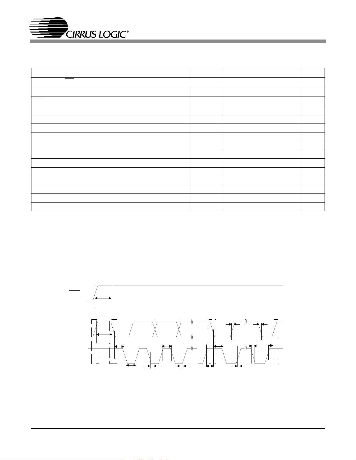
8.8.1 SPI Mode
In SPI mode, CS is the CS4224 chip select signal,
CCLK is the control port bit clock, CDIN is the input
data line from the microcontroller and the chip address is 0010000. All signals are inputs and data is
clocked in on the rising edge of CCLK.
Figure 6 shows the operation of the control port in
SPI mode. To write to a register, bring CS
first 7 bits on CDIN form the chip address, and
must be 0010000. The eighth bit is a read/write indicator (R/W
reading from the CS4224 is not supported in the
SPI mode. The next 8 bits form the Memory Address Pointer (MAP), which is set to the address of
the register that is to be updated. The next 8 bits
arethedatawhichwillbeplacedintoaregister
designated by the MAP.
), which must be low to write. Register
low. The
The CS4224 has a MAP auto increment capability,
enabled by the INCR bit in the MAP register. If
INCR is a zero, then the MAP will stay constant for
successive writes. If INCR is set to a 1, then MAP
will auto increment after each byte is written, allowing block writes of successive registers. Register
reading from the CS4224 is not supported in the
SPI mode.
8.8.2 I2CMode
In I2C mode, SDA is a bidirectional data line. Data
is clocked into and out of the part by the clock,
SCL, with the clock to data relationship as shown
in Figure 7. There is no CS
partialchipaddressandshouldbetiedtoVDor
DGND as desired. The upper 6 bits of the 7 bit address field must be 001000. In order to communicate with the CS4224, the LSB of the chip address
field (first byte sent to the CS4224) should match
the setting of the AD0 pin. The eighth bit of the address byte is the R/W
write). If the operation is a write, the next byte is the
Memory Address Pointer which selects the register
to be read or written. If the operation is a read, the
contents of the register pointed to by the Memory
Address Pointer will be output. Setting the auto increment bit in MAP, allows successive reads or
writes of consecutive registers. Each byte is separated by an acknowledge bit.
pin. Pin AD0 forms the
bit (high for a read, low for a
DS290F1 25
Page 26

CS4223 CS4224
8.9 Memory Address Pointer (MAP)
76543210
INCR
00000000
Reserved Reserved Reserved Reserved
8.9.1 AUTO-INCREMENT CONTROL (INCR)
Default = 0
0 - Disabled
1-Enabled
8.9.2 REGISTER POINTER (MAP)
Default = 000
CS
CCLK
CHIP
CDIN
ADDRESS
0010000 R/W
MAP DATA
MAP2 MAP1 MAP0
MSB LSB
byte 1 byte n
MAP = Memory Address Pointer
Figure 6. Control Port Timing, SPI mode
SDA
SCL
00100 0
Start Stop
ADDR
AD0
Figure 7. Control Port Timing, I2Cmode
ACK DATA 1-8 ACK DATA 1-8 ACK
R/W
26 DS290F1
Page 27

CS4223 CS4224
LRCK
SCLK
SDATA +3 +2 +1
MSB
-1 -2 -3 -4 -5
Left Channel
+5 +4
Master Slave
I2S, up to 24-bit data
XTI=256, 384,512 Fs (CS4223- 256 Fsonly)
LRCK = 4 to 50 kHz
SCLK = 64 Fs
LRCK
SCLK
SDATA +3 +2 +1
MSB
-1 -2 -3 -4 -5
Left Channel
+5 +4
LSB
MSB
-1 -2 -3 -4
I2S, up to 24-bit data
XTI = 256, 384, 512 Fs
LRCK = 4 to 50 kHz
SCLK = 48,64, 128 Fs
Figure 8. Serial Audio Format 0 (I2S)
LSB
MSB
-1 -2 -3 -4
Right Channel
+3 +2 +1
+5 +4
Right Channel
+3 +2 +1
+5 +4
LSB
LSB
Master Slave
Left-justified, up to 24-bit data
XTI=256, 384,512 Fs (CS4223-256Fsonly)
LRCK = 4 to 50 kHz
SCLK = 64 Fs
Figure 9. Serial Audio Format 1
LRCK
SCLK
SDATA
0
Left Channel
23 22 21 20 19 18
32 clocks
Master Slave
Right-justified, 24-bit data
XTI=256, 384,512 Fs (CS4223-256Fsonly)
LRCK = 4 to 50 kHz
SCLK = 64 Fs
Figure 10. Serial Audio Format 2
Left-justified, up to 24-bit data
XTI = 256, 384, 512 Fs
LRCK = 4 to 50 kHz
SCLK = 48, 64, 128 Fs
Right Channel
654321 07
23 22 21 20 19 18
65432 107
Right-justified, 24-bit data
XTI = 256, 384, 512 Fs
LRCK = 4 to 50 kHz
SCLK = 64 Fs
DS290F1 27
Page 28

CS4223 CS4224
LRCK
SCLK
SDATA
10 6543210987
17 16 17 16
19 18 19 18
Left Channel
15 14 13 12 11 10
32 clocks
Master Slave
Right-justified, 20-bit data
XTI=256, 384,512 Fs (CS4223-256Fs only)
LRCK = 4 to 50 kHz
SCLK = 64 Fs
6543210987
Right-justified, 20-bit data
XTI = 256, 384, 512 Fs
LRCK = 4 to 50 kHz
SCLK = 64 Fs
Figure 11. Serial Audio Format 3
Right Channel
15 14 13 12 11 10
Figure 12. Optional Input Buffer
150
Ω
AINR+
2.2 nF
Input
+
10 µF
CS4223/4
AINR-
4.7 µF
+
0.1 µF
Figure 13. Single-ended Input Application
28 DS290F1
Page 29

CS4223 CS4224
5
Figure 14. 2- and 3-Pole Butterworth Filters
Gain
dB
Analog Digital
0
Signal
Noise
Amplit ude (dB)
0 -113.
Attenuation (dB)
Figure 16. Hybrid Analog/Digital Attenuation
0dB
-10 dB
T1 = 50 µs
T2 = 15 µs
F1 F2
Frequency
Figure 15. De-emphasis Curve
DS290F1 29
Page 30

9. ADC/DAC FILTER RESPONSE
Figure 17. ADC Filter Response Figure 18. ADC Passband Ripple
CS4223 CS4224
Figure 19. ADC Transition Band Figure 20. DAC Filter Response
Figure 21. DAC Passband Ripple Figure 22. DAC Transition Band
30 DS290F1
Page 31

10.PARAMETER DEFINITIONS
Dynamic Range
The ratio of the full scale rms value of the signal to the rms sum of all other spectral components over the
specified bandwidth. Dynamic range is a signal-to-noise measurement over the specified bandwidth
made with a -60 dBFS signal. 60 dB is then added to the resulting measurement to refer the measurement
to full scale. This technique ensures that the distortion components are below the noise level and do not
affect the measurement. This measurement technique has been accepted by the Audio Engineering Society, AES17-1991, and the Electronic Industries Association of Japan, EIAJ CP-307.
Total Harmonic Distortion + Noise
The ratio of the rms value of the signal to the rms sum of all other spectral components over the specified
bandwidth (typically 20 Hz to 20 kHz), including distortion components. Expressed in decibels. ADCs are
measured at -1 dBFS as suggested in AES17-1991 Annex A and DACs are measured at 0 dBFS.
Idle Channel Noise / Signal-to-Noise-Ratio
The ratio of the rms analog output level with 1 kHz full scale digital input to the rms analog output level
with all zeros into the digital input. Measured A-weighted over a 10 Hz to 20 kHz bandwidth. Units in decibels. This specification has been standardized by the Audio Engineering Society, AES17-1991, and referred to as Idle Channel Noise. This specification has also been standardized by the Electronic Industries
Association of Japan, EIAJ CP-307, and referred to as Signal-to-Noise-Ratio.
CS4223 CS4224
Total Harmonic Distortion (THD)
THD is the ratio of the test signal amplitude to the rms sum of all the in-band harmonics of the test signal.
Units in decibels.
Interchannel Isolation
A measure of crosstalk between channels. Measured for each channel at the converter's output with no
signal to the input under test and a full-scale signal applied to the other channel. Units in decibels.
Frequency Response
A measure of the amplitude response variation from 20 Hz to 20 kHz relative to the amplitude response
at 1 kHz. Units in decibels.
Interchannel Gain Mismatch
For the ADCs, the difference in input voltage that generates the full scale code for each channel. For the
DACs, the difference in output voltages for each channel with a full scale digital input. Units are in decibels.
Gain Error
The deviation from the nominal full scale output for a full scale input.
Gain Drift
The change in gain value with temperature. Units in ppm/°C.
Offset Error
For the ADCs, the deviation in LSB's of the output from mid-scale with the selected inputs tied to a common potential. For the DAC's, the differential output voltage with mid-scale input code. Units are in volts.
DS290F1 31
Page 32
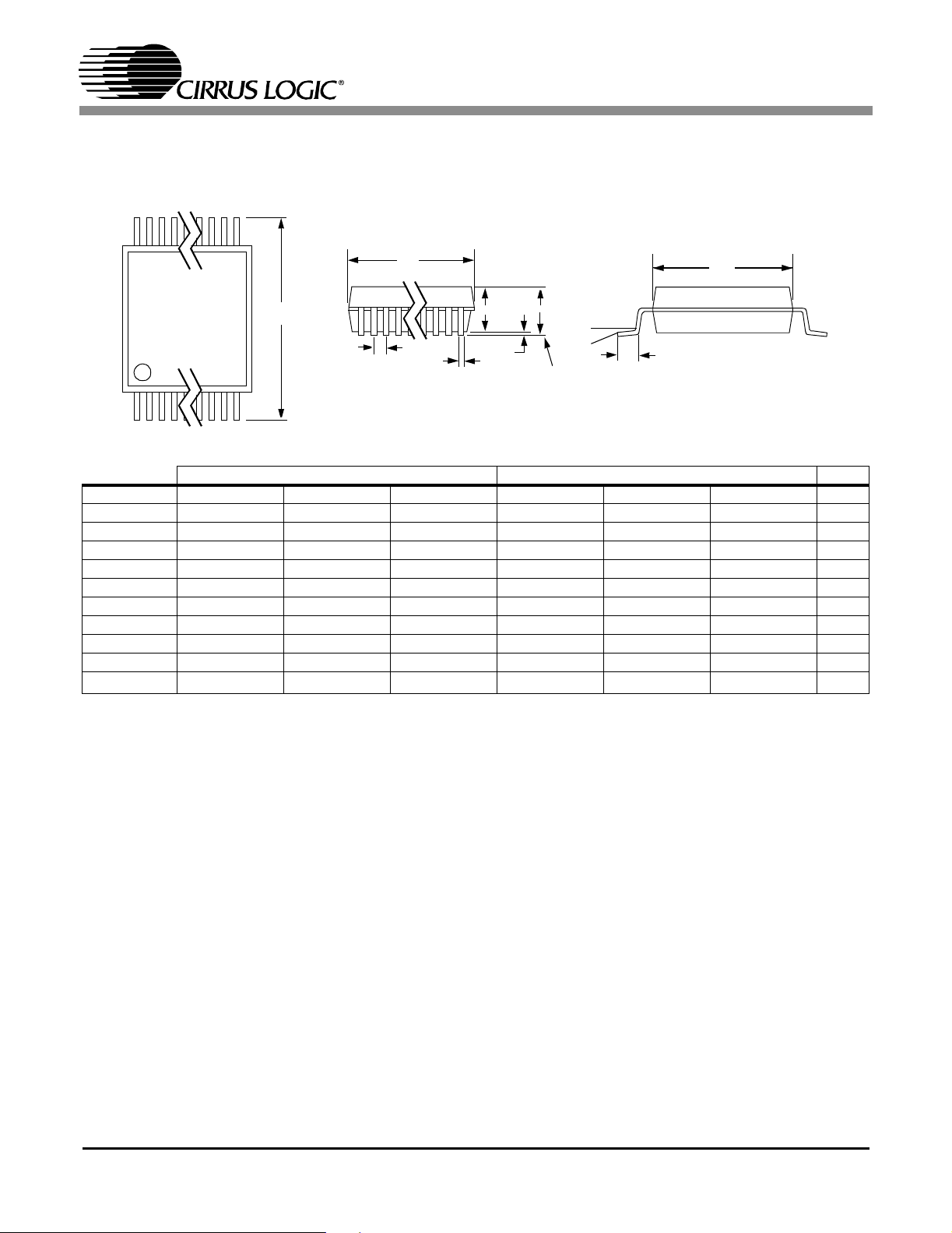
11.PACKAGE DIMENSIONS
28L SSOP PACKAGE DRAWING
N
CS4223 CS4224
D
E
A2
A
E1
1
∝
2
b
SIDE VIEW
1
23
e
TOP VIEW
INCHES MILLIMETERS NOTE
DIM MIN NOM MAX MIN NOM MAX
A -- -- 0.084 -- -- 2.13
A1 0.002 0.006 0.010 0.05 0.15 0.25
A2 0.064 0.069 0.074 1.62 1.75 1.88
b 0.009 -- 0.015 0.22 -- 0.38 2,3
D 0.390 0.4015 0.413 9.90 10.20 10.50 1
E 0.291 0.307 0.323 7.40 7.80 8.20
E1 0.197 0.209 0.220 5.00 5.30 5.60 1
e 0.022 0.026 0.030 0.55 0.65 0.75
L 0.025 0.0354 0.041 0.63 0.90 1.03
∝
0° 4° 8° 0° 4° 8°
A1
SEATING
PLANE
L
END VIEW
JEDEC #: MO-150
Controlling Dimension is Millimeters
Notes: 1. “D” and “E1” are reference datums and do not included mold flash or protrusions, but do include mold
mismatch and are measured at the parting line, mold flash or protrusions shall not exceed 0.20 mm per
side.
2. Dimension “b” does not include dambar protrusion/intrusion. Allowable dambar protrusion shall be
0.13 mm total in excess of “b” dimension at maximum material condition. Dambar intrusion shall not
reduce dimension “b” by more than 0.07 mm at least material condition.
3. These dimensions apply to the flat section of the lead between 0.10 and 0.25 mm from lead tips.
32 DS290F1
Page 33

• Notes •
Page 34

 Loading...