

Page 1
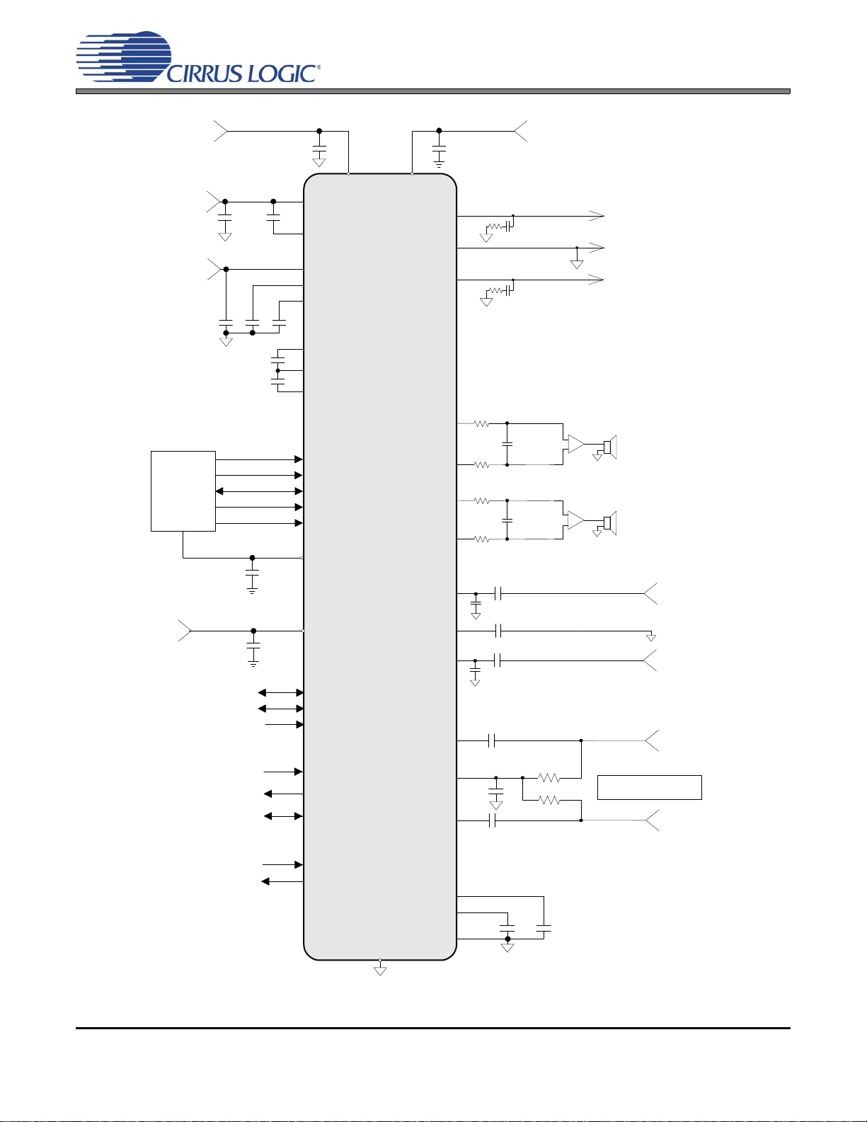
CS4207
Low-power, 4-in / 6-out HD Audio Codec with Headphone Amp
DIGITAL to ANALOG FEATURES
DAC1 (Headphone)
– 101 dB Dynamic Range (A-wtd)
– -89 dB THD+N
Headphone Amplifier - GND Centered
– Integrated Negative-voltage Regulator
– No DC-blocking Capacitor Required
– 50 mW Power/Channel into 16
DAC2 & DAC3 (Line Outs)
– 110 dB Dynamic Range (A-wtd)
– -94 dB THD+N
– Differential Balanced or Single-ended
Each DAC Supports 32 kHz to 192 kHz Sample
Rates Independently.
Digital Volume Control
– +6.0 dB to -57.5 dB in 0.5 dB Steps
– Zero Cross and/or Soft Ramp Transitions
Independent Support of D0 and D3 Power
States for Each DAC
Fast D3 to D0 Transition
– Audio Playback in Less Than 50 ms
ANALOG to DIGITAL FEATURES
ADC1 & ADC2
– 105 dB Dynamic Range (A-wtd)
– -88 dB THD+N
– Differential Balanced or Single-ended
Inputs
– Analog Programmable Gain Amplifier
(PGA) ±12 dB, 1.0 dB Steps, with Zero
Cross Transitions and Mute
MIC Inputs
– Pre-amplifier with Selectable 0 dB, +10 dB,
+20 dB, and +30 dB Gain Settings
– Programmable, Low-noise MIC Bias Level
Each ADC Supports 8 kHz to 96 kHz Sample
Rates Independently
Additional Digital Attenuation Control
– -13.0 dB to -51.0 dB in 1.0 dB steps
– Zero Cross and/or Soft Ramp Transitions
Digital Interface for Two Dual Digital Mic Inputs
Independent Support of D0 and D3 Power
States for Each ADC
HD Audio
Bus
VL_HD
(1.5 V to 3.3 V)
S/PDIF OUT 2
S/PDIF OUT 1
VL_IF
(3.3 V)
S/PDIF IN
D-Mic Clock
D-Mic In
Level Translator
Level Translator
http://www.cirrus.com
Interface
HD Bus
Fs
HD
Audio
GPIOGPIO
SPDIF
TX 2
SPDIF
TX 1
SPDIF
RX
(1.5 V to 1.8 V)
128Fs Clock
Multiplier
SPDIF
RX SRC
VD
Vol/Mute
Vol/Mute
Vol/Mute
Vol/Boost/
Mute
Vol/Boost/
Mute
SRC &
Multibit
Modulator
SRC &
Multibit
Modulator
SRC &
Multibit
Modulator
Digital
Filter &
SRC
Digital
Filter &
SRC
Copyright Cirrus Logic, Inc. 2012
(All Rights Reserved)
VA, VA_REF
(3.3 V to 5.0 V)
2-Chnl
DAC1
2-Chnl
DAC2
2-Chnl
DAC3
2-Chnl
ADC1
2-Chnl
ADC2
Jack
Sense
VA_HP
(3.3 V to 5.0 V)
Chrg
Pump
Buck
+VHP
Headphone
Amp - GND
Centered
Line
Out
Line
Out
Pump
Invert
PGA
PGA
MIC
Bias
Chrg
-VHP
Left HP Out
Right HP Out
+
Left Line Out
+
Right Line Out
+
Left Line Out
+
Right Line Out
+
Line/Mic In L
-
Line/Mic In R
+
+
Mic/Line In L
+
Mic/Line In R
-
Mic Bias
SENSE_A
AUG '12
DS880F4
Page 2

CS4207
Digital Audio Interface Receiver
Complete EIAJ CP1201, IEC 60958, S/PDIF
Compatible Receiver
32 kHz to 192 kHz Sample Rate Range
Automatic Detection of Compressed Audio
Streams
Integrated Sample Rate Converter
– 128 dB Dynamic Range
– -120 dB THD+N
– Supports Sample Rates up to 192 kHz
– 1:1 Input/Output Sample Rate Ratios
Digital Audio Interface Transmitters
Two Independent EIAJ CP1201, IEC-60958,
S/PDIF Compatible Transmitters
32 kHz to 192 kHz Sample Rate Range
System Features
Very Low D3 Power Dissipation of <7 mW
– Jack Detect Active in D3
– HDA BITCLK Not Required for D3 State
Jack Detect Does Not Require HDA Bus
BITCLK
All Configuration Settings are Preserved in D3
State
Pop/Click Suppression in State Transitions
Detects Wake Event and Generates Power
State Change Request when HDA Bus
Controller is in D3
Variable Power Supplies
– 1.5 V to 1.8 V Digital Core Voltage
– 3.3 V to 5.0 V Analog Core Voltage
– 3.3 V to 5.0 V Headphone Drivers
– 1.5 V to 3.3 V HD Bus Interface Logic
– 3.3 V Interface Logic levels for GPIO,
S/PDIF, and Digital Mic
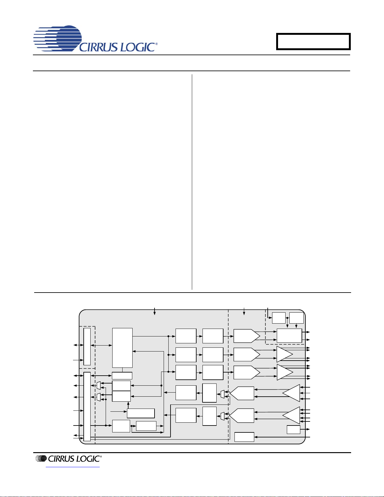
General Description
The CS4207 is a highly integrated multi-channel lowpower HD Audio Codec featuring 192 kHz DACs,
96 kHz ADCs, 192 kHz S/PDIF Transmitters and Receiver, Microphone pre-amp and bias voltage, and a
ground centered Headphone driver. Based on multi-bit,
delta-sigma modulation, it allows infinite sample rate
adjustment between 32 kHz and 192 kHz.
The ADC input path allows contro l of a number of features. The microphone input path includes a selectable
programmable-gain pre-amplifier stage and a low- noise
MIC bias voltage supply. A PGA is available for line and
microphone inputs and provides analog gain with soft
ramp and zero cross transitions. The ADC also features
an additional digital volume attenuator with soft ramp
transitions.
The stereo headphone amplifier is powered from a separate internally generated positive supply, with an
integrated charge pump providing a negative supply.
This allows a ground-centered analog output with a
wide signal swing and eliminates external DC-blo cking
capacitors.
The integrated digital audio interface receiver and transmitters utilize a 24-bit, high-performance, monolithic
CMOS stereo asynchronous sample rate converter to
clock align the PCM samples to/from the S/PDIF interfaces. Auto detection of non-PCM encoded data
disables the sample rate conversion to preserve bit accuracy of the data.
In addition to its many features, the CS4207 operates
from a low-voltage analog and digital core, making this
part ideal for portable systems that require low power
consumption in a minimal amount of space.
The CS4207 is available in a 48-pin WQFN package in
both Automotive (-40°C to +105°C) and Commercial
(-40°C to +85°C) grades. The CS4207 Customer Demonstration board is also available for device evaluation
and implementation suggestions. Please refer to “Or-
dering Information” on p 147 for complete ordering
information.
Individual Power-down Managed
– ADCs, DACs, PGAs, Headphone Driver,
S/PDIF Receiver, and Transmitters
2 DS880F4
Page 3

TABLE OF CONTENTS
1. PIN DESCRIPTIONS .............................................................................................................................. 8
1.1 CS4207 48-pin QFN Pinout: ....................................... .......................................... ........................... 8
1.2 Digital I/O Pin Characteristics .............................. .... ... ... ... .... ... ... ................................................... 10
2. TYPICAL CONNECTION DIAGRAMS .................................................................................................11
3. CHARACTERISTICS AND SPECIFICATIONS .................................................................................... 13
RECOMMENDED OPERATING CONDITIONS .................................................................................. 13
ABSOLUTE MAXIMUM RATINGS ...................................................................................................... 13
ANALOG INPUT CHARACTERISTICS (COMMERCIAL - CNZ) ......................................................... 14
ANALOG INPUT CHARACTERISTICS (AUTOMOTIVE - DNZ) ......................................................... 15
ADC DIGITAL FILTER CHARACTERISTICS ...................................................................................... 16
ANALOG OUTPUT CHARACTERISTICS (COMMERCIAL - CNZ) ..................................................... 17
ANALOG OUTPUT CHARACTERISTICS (AUTOMOTIVE - DNZ) ..................................................... 19
COMBINED DAC INTERPOLATION & ON-CHIP ANALOG FILTER RESPONSE ............................. 21
DC ELECTRICAL CHARACTERISTICS . ... ... .... ... ... ... .......................................... ................................ 21
DIGITAL MICROPHONE INTERFACE CHARACTERISTICS ............................................................. 22
DIGITAL INTERFACE SPECIFICATIONS & CHARACTERISTICS .................................................... 23
HD AUDIO BUS SPECIFICATIONS & CHARACTERISTICS .............................................................. 23
S/PDIF TRANSMITTER/RECEIVER SPECIFICATIONS & CHARACTERISTICS .............................. 23
POWER CONSUMPTION ................................................................................................................... 24
4. CODEC RESET AND INITIALIZATION ............................................................................................... 25
4.1 Link Reset ................................................................... .......................................... ......................... 25
4.2 Function Group Reset .................................... ... .......................................... ................................... 25
4.3 Codec Initialization ............................... ... .... ... ... .......................................... ................................... 25
4.4 D3 Lower Power State Support ........ .......................................... .......................................... ......... 26
4.5 Extended Power States Supported (EPSS) ................................................................................... 26
4.6 Power State Settings Reset (PS-SettingsReset) ........................................................................... 28
4.7 Register Settings Across Resets ................................................................................................... 29
5. PRESENCE DETECTION ..................................................................................................................... 31
5.1 Jack Detection Circuit .................................................................................................................... 31
5.1.1 Presence Detection and Unsolicited Response .................................................................... 31
5.1.2 S/PDIF Receiver Presence Detect ........................................................................................ 32
6. HD AUDIO CODEC SUPPORTED VERBS AND RESPONSES ......................................................... 33
6.1 Software Programming Model .......................................................................................................33
6.1.1 Node ID Summary ................................................................................................................. 34
6.1.2 Pin Configuration Register Defaults ......................................................................................35
6.2 Root Node (Node ID = 00h) ........................................................................................................... 36
6.2.1 Vendor and Device ID ..................................................... ... ... ... .... ... ... ................................... 36
6.2.2 Revision ID ............................................................................................................................ 36
6.2.3 Subordinate Node Count ....................................................................................................... 36
6.3 Audio Function Group (Node ID = 01h) ......................................................................................... 37
6.3.1 Subordinate Node Count ....................................................................................................... 37
6.3.2 Function Group Type ............................................................................................................. 37
6.3.3 Audio Function Group Capabilities ........................................................................................37
6.3.4 Supported PCM Size, Rates ...............................................................................................
6.3.5 Support
6.3.6 Supported Power States ....................................................................................................... 39
6.3.7 GPIO Capabilities .................................................................................................................. 40
6.3.8 Power States ......................................................................................................................... 41
6.3.9 GPIO Data ............................................................................................................................. 42
6.3.10 GPIO Enable Mask .............................. .......................................... ...................................... 43
6.3.11 GPIO Direction .......................................... .... ... ... ... .... ... .......................................... ............ 43
6.3.12 GPIO Sticky Mask ............................................ ... ... .... ... ... ... ... ............................................. 43
e
CS4207
.. 38
d Stream Formats ................................................................................................... 39
DS880F4 3
Page 4

CS4207
6.3.13 Implementation Identification ............................................................................................... 44
6.3.14 Function Reset .................................................................................................................... 44
6.4 DAC1, DAC2, DAC3 Output Converter Widgets (Node ID = 02h, 03h, 04h) ................................. 45
6.4.1 Audio Widget Capabilities ........... ... .... ... ... ... .... ... .......................................... ......................... 45
6.4.2 Supported PCM Size, Rates .............. ... ... ... .... ... ... ... .......................................... ................... 46
6.4.3 Supported Stream Formats ...... ... .......................................... .......................................... ...... 46
6.4.4 Supported Power States ................ .......................................... ............................................. 47
6.4.5 Output Amplifier Capabilities ................................................................................................. 47
6.4.6 Power States ......... ... .......................................... .......................................... ......................... 48
6.4.7 Converter Stream, Channel ................................................................................................... 49
6.4.8 Converter Format ............................................ ... ... ... .... ... ... ... ................................................ 49
6.4.9 Amplifier Gain/Mute ..................... .................................... ................................... ................... 51
6.5 ADC1, ADC2 Input Converter Widgets (Node ID = 05h, 06h) ....................................................... 53
6.5.1 Audio Widget Capabilities ........... ... .... ... ... ... .... ... .......................................... ......................... 53
6.5.2 Supported PCM Size, Rates .............. ... ... ... .... ... ... ... .......................................... ................... 54
6.5.3 Supported Stream Formats ...... ... .......................................... .......................................... ...... 54
6.5.4 Input Amplifier Capabilities .............................. .......................................... ............................ 55
6.5.5 Connection List Length ....................... ... ... ... .... ... ... ... .......................................... ................... 55
6.5.6 Supported Power States ................ .......................................... ............................................. 56
6.5.7 ADC1 Connection List Entry ..................................................................................................56
6.5.8 ADC1 Connection Select Control .......................................................................................... 56
6.5.9 ADC2 Connection List Entry ..................................................................................................57
6.5.10 ADC2 Connection Select Control ........... ................................................................. ............57
6.5.11 Power States ....................................................................................................................... 58
6.5.12 Converter Stream, Channel ................................................................................................. 59
6.5.13 Converter Format ................................................................................................................ 59
6.5.14 Amplifier Gain/Mute ............................................................................................................. 61
6.6 S/PDIF Receiver Input Converter Widget (Node ID = 07h) ........................................................... 63
6.6.1 Audio Widget Capabilities ........... ... .... ... ... ... .... ... .......................................... ......................... 63
6.6.2 Supported PCM Size, Rates .............. ... ... ... .... ... ... ... .......................................... ................... 64
6.6.3 Supported Stream Formats ...... ... .......................................... .......................................... ...... 64
6.6.4 Connection List Length ....................... ... ... ... .... ... ... ... .......................................... ................... 65
6.6.5 Supported Power States ................ .......................................... ............................................. 65
6.6.6 Connection List Entry ............................................................................................................ 65
6.6.7 Power States ......... ... .......................................... .......................................... ......................... 66
6.6.8 Converter Stream, Channel ................................................................................................... 67
6.6.9 Converter Format ............................................ ... ... ... .... ... ... ... ................................................ 67
6.6.10 Digital Converter Control ..................................................................................................... 69
6.7 S/PDIF Transmitter 1, S/PDIF Transmitter 2 Output Converter Widgets (Node ID = 08h, 14h) .... 70
6.7.1 Audio Widget Capabilities ........... ... .... ... ... ... .... ... .......................................... ......................... 70
6.7.2 Supported PCM Size, Rates .............. ... ... ... .... ... ... ... .......................................... ................... 71
6.7.3 Supported Stream Formats ...... ... .......................................... .......................................... ...... 72
6.7.4 Supported Power States ................ .......................................... ............................................. 72
6.7.5 Power States ......... ... .......................................... .......................................... ......................... 72
6.7.6 Converter Stream, Channel ................................................................................................... 74
6.7.7 Converter Format ............................................ ... ... ... .... ... ... ... ................................................ 74
6.7.8 Digital Converter Control ....................................................................................................... 76
6.8 Headphone Pin Widget (Node ID = 09h) .......................................................................................78
...
6.8.1 Audio Widget Capabilities ........... ... .... ... ... ... .... ... .......................................... ......................
6.8.2 Pin Capabilities ...................... ... ... ... .... ... ... ... .......................................... ................................ 78
6.8.3 Connection List Length ....................... ... ... ... .... ... ... ... .......................................... ................... 79
6.8.4 Supported Power States ................ .......................................... ............................................. 79
6.8.5 Connection List Entry ............................................................................................................ 80
6.8.6 Power States ......... ... .......................................... .......................................... ......................... 80
78
4 DS880F4
Page 5

CS4207
6.8.7 Pin Widget Control ................................................................................................................ 81
6.8.8 Unsolicited Response Control ............................................................................................... 82
6.8.9 Pin Sense .............................................................................................................................. 83
6.8.10 Configuration Default .............................. .......................................... ................................... 83
6.9 Line Out 1 Pin Widget (Node ID = 0Ah) ...................... .......................................... ......................... 85
6.9.1 Audio Widget Capabilities ..................................................................................................... 85
6.9.2 Pin Capabilities ...................................................................................................................... 86
6.9.3 Connection List Length .......................................................................................................... 86
6.9.4 Supported Power States ....................................................................................................... 87
6.9.5 Connection List Entry ............................................................................................................ 87
6.9.6 Power States ......................................................................................................................... 87
6.9.7 Pin Widget Control ................................................................................................................ 88
6.9.8 Unsolicited Response Control ............................................................................................... 89
6.9.9 Pin Sense .............................................................................................................................. 90
6.9.10 EAPD/BTL Enable ............................................................................................................... 90
6.9.11 Configuration Default .............................. .......................................... ................................... 91
6.10 Line Out 2 Pin Widget (Node ID = 0Bh) ....................................................................................... 92
6.10.1 Audio Widget Capabilities ...................... ... .... ... ... ... .... ... ... ... ... .... ... ... ....... ... ... ... ... .... ... ... . ..... 92
6.10.2 Pin Capabilities .......................... ... .... ... ... ... .... ... .......................................... ......................... 93
6.10.3 Connection List Length ..................................... .......................................... ......................... 93
6.10.4 Connection List Entry ................................................. ... ... ... ... .... ... ... ................................... 94
6.10.5 Pin Widget Control .................... .......................................... ................................................ 94
6.10.6 EAPD/BTL Enable ............................................................................................................... 95
6.10.7 Configuration Default .............................. .......................................... ................................... 96
6.11 Line In 1/Mic In 2, Mic In 1/Line In 2 Pin Widgets (Node ID = 0Ch, 0Dh) .................................... 97
6.11.1 Audio Widget Capabilities ...................... ... .... ... ... ... .... ... ... ... ... .... ... ... ....... ... ... ... ... .... ... ... . ..... 97
6.11.2 Line In 1/Mic In 2 Pin Capabilities .............................................................. ... ... ... ....... ... ...... 97
6.11.3 Mic In 1/Line In 2 Pin Capabilities .............................................................. ... ... ... .... ... ... ...... 98
6.11.4 Input Amplifier Capabilities ............................ ................................... ................................... 99
6.11.5 Supported Power States ..................... .......................................... ...................................... 99
6.11.6 Power States ....... ... .......................................... .......................................... ......................... 99
6.11.7 Line In 1/Mic In 2 Pin Widget Control ......................... ... ... ... ... .... ... ... ... .... ... ... ... ... .... ...... ... . 101
6.11.8 Mic In 1/Line In 2 Pin Widget Control .................. ....... ... ... ... ... .... ... ... ... .... ... ... ... ... .... ... ... .... 101
6.11.9 Unsolicited Response Control ................ ........................................................................... 102
6.11.10 Pin Sense ........................................................................................................................ 103
6.11.11 Mic In 1/Line In 2 EAPD/BTL Enable .............................................................................. 104
6.11.12 Line In 1/Mic In 2 Configuration Default .......................................................................... 104
6.11.13 Mic In 1/Line In 2 Configuration Default ..........................................................................105
6.11.14 Amplifier Gain/Mute ......................................................................................................... 106
6.12 Digital Mic In 1, Digital Mic In 2 Pin Widgets (Node ID = 0Eh, 12h) .... ... ... ... .... .......................... 108
6.12.1 Audio Widget Capabilities ...................... ... .... ... ... ... .... ... ... ... ... ....... ... ... .... ... ... ... ... .... ... ... .... 108
6.12.2 Pin Capabilities .......................... ... .... ... ... ... .... ... .......................................... ....................... 109
..
6.12.3 Input Amplifier Capabilities
6.12.4 Pin Widget Control .................... .......................................... .............................................. 110
6.12.5 Digital Mic In 1 Configuration Default ................................................................................ 110
6.12.6 Digital Mic In 2 Configuration Default ................................................................................ 111
6.12.7 Amplifier Gain/Mute ... ........................................................................................................ 112
6.13 S/PDIF Receiver Input Pin Widget (Node ID = 0Fh) ....... ........................................................... 114
6.13.1 Audio Widget Capabilities ...................... ... .... ... ... ... .... ... ... ... ... .... ... ... ....... ... ... ... ... .... ... ... . ... 114
6.13.2 Pin Capabilities .......................... ... .... ... ... ... .... ... .......................................... ....................... 115
6.13.3 Supported Power States ..................... .......................................... .................................... 115
6.13.4 Power States ....... ... .......................................... .......................................... ....................... 116
6.13.5 Pin Widget Control .................... .......................................... .............................................. 117
6.13.6 Unsolicited Response Control ................ ........................................................................... 117
....................................... ................................... .................... 109
DS880F4 5
Page 6

CS4207
6.13.7 Pin Sense .......................................................................................................................... 118
6.13.8 Configuration Default ......................................................................................................... 119
6.14 S/PDIF Transmitter 1, S/PDIF Transmitter 2 Output Pin Widgets (Node ID = 10h, 15h) ........... 120
6.14.1 Audio Widget Capabilities ................................................................................................. 120
6.14.2 Pin Capabilities .................................................................................................................. 121
6.14.3 Connection List Length ...................................................................................................... 121
6.14.4 S/PDIF Transmitter 1 Connection List Entry ..................................................................... 122
6.14.5 S/PDIF Transmitter 2 Connection List Entry ..................................................................... 122
6.14.6 Pin Widget Control ............................................................................................................ 123
6.14.7 S/PDIF Transmitter 1 Configuration Default ...................................................................... 124
6.14.8 S/PDIF Transmitter 2 Configuration Default ...................................................................... 125
6.15 Vendor Processing Widget (Node ID = 11h) .............................................................................. 126
6.15.1 Audio Widget Capabilities ................................................................................................. 126
6.15.2 Processing Capabilities ..................................................................................................... 126
6.15.3 Processing State ............................................................................................................... 127
6.15.4 Coefficient Index ................................................................................................................ 127
6.15.5 Processing Coefficient ....................................................................................................... 128
6.15.6 Coefficient Registers ......................................................................................................... 128
6.15.6.1 S/PDIF RX/TX Interface Status (CIR = 0000h) .................. ... ... .... ... ... ... ... .... ... ... ... . 129
6.15.6.2 S/PDIF RX/TX Interface Control (CIR = 0001h) ...................................... .... ... ....... 130
6.15.6.3 ADC Configuration (CIR = 0002h) ........................................................................ . 131
6.15.6.4 DAC Configuration (CIR = 0003h) ........................................................................ . 134
6.15.6.5 Beep Configuration (CIR = 0004h) ........................................................................ 135
6.16 Beep Generator Widget (Node ID = 13h) .................................................................................. 136
6.16.1 Audio Widget Capabilities ................................................................................................. 136
6.16.2 Beep Generation Control ........................ ... .... ... ... ... .......................................... ... .............. 137
7. APPLICATIONS ................................................................................................................................. 138
7.1 HD Audio Interface ....................................................................................................................... 138
7.1.1 Multi-Channel Streams ................................ .... ... ... ... .... ... ... .......................................... ....... 138
7.2 Analog Inputs ............................................................................................................................... 139
7.3 Analog Outputs ............................................................................................................................ 142
7.3.1 Output Filter .............................. .......................................... ................................................. 142
7.3.2 Analog Supply Removal ..... ... ... .......................................... .......................................... ... .... 142
7.4 Digital Mic Inputs .......................................................................................................................... 142
7.5 S/PDIF Input and Outputs ............................................................................................................ 143
7.5.1 S/PDIF Receiver SRC .........................................................................................................143
8. PCB LAYOUT CONSIDERATIONS ...................................................................................................144
8.1 Power Supply, Grounding ............................................................................................................ 144
8.2 QFN Thermal Pad ........................................................................................................................144
9. PARAMETER DEFINITIONS .............................................................................................................. 145
10. QFN PACKAGE DIMENSIONS ........................................................................................................ 146
THERMAL CHARACTERISTICS ....................................................................................................... 146
11. ORDERING INFORMATION ............................................................................................................ 147
12. REFERENCES .................................................................................................................................. 147
13. REVISION HISTORY ........................................................................................................................ 148
6 DS880F4
Page 7

LIST OF FIGURES
Figure 1.Typical Connection Diagram - Desktop System ......................................................................... 11
Figure 2.Typical Connection Diagram - Portable System ......................................................................... 12
Figure 3.Output Test Load, Headphone Out ............................................................................................. 18
Figure 4.Output Test Load, Line Out ......................................................................................................... 18
Figure 5.Output Test Load, Headphone Out ............................................................................................. 20
Figure 6.Output Test Load, Line Out ......................................................................................................... 20
Figure 7.Digital MIC Interface Timing ........................................................................................................ 22
Figure 8.PS-SettingsReset Behavior ........................................................................................................ 28
Figure 9.Jack Presence Detect Circuit ...................................................................................................... 31
Figure 10.Software Programming Model .................................................................................................. 33
Figure 11.Single-Ended Input Filter ........................................................................................................ 139
Figure 12.Pseudo-Differential Input Filter ............................................................................................... 140
Figure 13.Differential Input Filter ............................................................................................................. 141
Figure 14.Differential to Single-Ended Output Filter ........... ... ... ... .... ...... ... ... .... ... ... ... .... ... ... ... ... .... ... .. ..... 142
Figure 15.Passive Single-Ended Output Filter ........................................................................................ 142
LIST OF TABLES
Table 1. Register Settings Across Reset Conditions ................................................................................ 29
Table 2. Device Node ID Summary ........................... ... .......................................... ................................... 34
Table 3. Pin Configuration Register Defaults ............................................................................................ 35
Table 4. Stream Format Examples ......................................................................................................... 138
Table 5. Line In 1/Mic In 2 Input Topology Register Settings .............................. ............. ............. .......... 139
Table 6. Mic In 1/Line In 2 Input Topology Register Settings .................................................................. 139
CS4207
DS880F4 7
Page 8
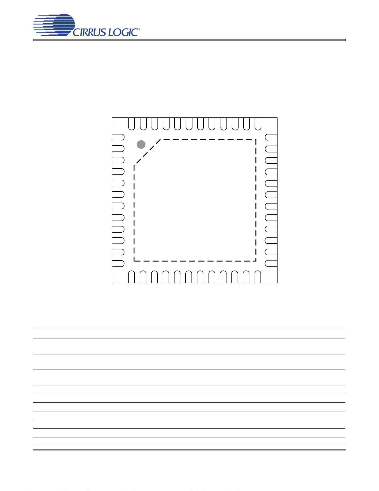
1. PIN DESCRIPTIONS
HPREF
Thermal Pad
1413
8
7
6
5
4
3
2
1
15
16
17 18 19 20
29
30
31
32
33
34
35
36
41
424344
45
464748
37
38
3940
12
11
10
9
21 22 23 24
25
26
27
28
SPDIF_OUT1
SENSE_A
VL_IF
LINEOUT_R1+
Top-Down (Through Package) View
48-Pin QFN Package
LINEOUT_L1+
LINEOUT_L1-
LINEOUT_R2-
LINEOUT_R2+
LINEOUT_L2+
LINEOUT_L2-
VBIAS (DAC)
VCOM
VREF+ (ADC)
AGND
VA
SPDIF_IN
FLYN
FLYC
VHP_FILT-
FLYP
HPOUT_L
HPREF
HPOUT_R
VA_HP
LINEOUT_R1-
GPIO0/DMIC_SDA1
VL_HD
DMIC_SCL
SDO
BITCLK
DGND
SDI
VD
SYNC
RESET#
GPIO1/DMIC_SDA2
/SPDIF_OUT2
MICBIAS
MICIN_L-
MICIN_L+
MICIN_R+
GPIO2
GPIO3
MICIN_R-
LINEIN_L+
LINEIN_C-
LINEIN_R+
VA_REF
VHP_FILT+
HPGND
1.1 CS4207 48-pin QFN Pinout:
CS4207
Pin Name QFN Pin Description
VL_IF 1
GPIO0/
DMIC_SDA1
VL_HD 3
DMIC_SCL 4 Digital Mic Clock (Output) - The high speed clock output to the digital microphone.
SDO 5 Serial Data Input (Input) - Serial data input stream from the HD Audio Bus.
BITCLK 6 Bit Clock (Input) - 24 MHz bit clock from the HD Audio Bus.
DGND 7 Digital Ground (Input) - Ground reference for the internal digital section.
SDI 8 Serial Data Output (Input/Output) - Serial data output stream to the HD Audio Bus.
VD 9 Digital Power (Input) - Positive power for the internal digital section.
SYNC 10 Sync Clock (Input) - 48 kHz sync clock from the HD Audio Bus.
8 DS880F4
2
Digital Interface Signal Level (Input) - Digital supply for the GPIO, S/PDIF and Digital Mic inter-
faces. Refer to the Recommended Operating Conditions for appropriate voltages.
General Purpose I/O (Input/Output) - General purpose input or output line, or
Digital Mic Data Input (Input) - The first data input line from a digital microphone.
Digital Interface Signal Level (Input) - Digital supply for the HD Audio interface. Refer to the
Recommended Operating Conditions for appropriate voltages.
Page 9

CS4207
Pin Name QFN Pin Description
RESET# 11 Reset (Input) - The device enters a low power mode when this pin is driven low.
GPIO1/
DMIC_SDA2/
SPDIF_OUT2
SENSE_A 13 Jack Sense Pin (Input/Output) - Jack sense detect.
GPIO2 14 General Purpose I/O (Input/Output) - General purpose input or output lines.
GPIO3 15 General Purpose I/O (Input/Output) - General purpose input or output lines.
MICBIAS 16
MICIN_L-
MICIN_L+
MICIN_R+
MICIN_R-
LINEIN_L+
LINEIN_CLINEIN_R+
VA_REF
VA
AGND 26 Analog Ground (Input) - Ground reference for the internal analog section.
VREF+ 27 Positive Voltage Reference (Ou
VCOM 28 Quiescent Voltage (Output) - Filter connection for internal quiescent voltage.
VBIAS 29 Positive Voltage Reference (Output) - Positive reference voltage for the internal DACs.
LINEOUT_L2-
LINEOUT_L2+
LINEOUT_R2+
LINEOUT_R2LINEOUT_L1LINEOUT_L1+
LINEOUT_R1+
LINEOUT_R1-
HPOUT_L
HPOUT_R
HPREF 39 Pseudo Diff. Headphone Reference (Input) - Ground reference for the headphone amplifiers.
VHP_FILT- 41
FLYN 42
FLYC 43
VHP_FILT+ 44
FLYP 45
VA_HP 46
SPDIF_IN 47 S/PDIF Input (Input) - Input to internal S/PDIF Receiver.
SPDIF_OUT1 48 S/
HPGND TP
12
17
18
19
20
21
22
23
24
25
30
31
32
33
34
35
36
37
38
40
General Purpose I/O (Input/Output) - General purpose input or output line, or
Digital Mic Data Input (Input) - The second data input line from a digital microphone, or
S/PDIF Output (Output) - Output from internal S/PDIF Transmitter.
Microphone Bias (Output) - Provides a low noise bias supply for an external microphone. Elec-
trical characteristics are specified in the DC Electrical Characteristics table.
Microphone Input Left/Right (Input) - The full-scale level is specified in the ADC Analog Characteristics specification table.
Analog Input (Input) - The full-scale level is specified in the ADC Analog Characteristics specification table.
Analog Power (Input) - Positive power for the internal analog section. VA_REF is the return pin
for the VBIAS cap.
tp
ut) - Positive reference voltage for the internal ADCs.
Analog Audio Output (Output) - The full-scale output level is specified in the DAC Analog Char-
acteristics specification table
Analog Headphone Output (Output) - The full-scale output level is specified in the DAC Analog
Characteristics specification table.
Inverting Charge Pump Filter Connection (Output) - Power suppl y from the inverting charge
pump that provides the negative rail for the headphone amplifier.
Charge Pump Cap Negative Node (Output) - Negative node for the inverting charge pump’s flying capacitor.
Charge Pump Cap Common Node (Output) - Common positive node for the step-down and
inverting charge pumps’ flying capacitor.
Non-Inverting Charge Pump Filter Connection (Output) - Power supply from the step-down
charge pump that provides the positive rail for the headphone amplifier.
Charge Pump Cap Positive Node (Output) - Positive node for the step-down charge pump’s flying capacitor.
Analog Power For Headphone (Input) - Positive power for the internal analog headphone section.
Output (Output) - Output from internal S/PDIF Transmitter.
PDIF
HP Ground (Input) - Ground reference for the internal headphone section. See “QFN Thermal
Pad” on page 144 for more information.
DS880F4 9
Page 10
1.2 Digital I/O Pin Characteristics
Input and output levels and associated power supply voltage are shown in the table below. Logic levels
should not exceed the corresponding power supply voltage.
CS4207
Notes:
Power
Supply
VL_HD
VA SENSE_A Input - 3.3 V - 5.0 V
VL_IF
Pin Name
SW/(HW)
RESET# Input - 1.5 V - 3.3 V
SDO Input - 1.5 V - 3.3 V
BITCLK Input - 1.5 V - 3.3 V
SDI (Note 1) Input/Output 1.5 V - 3.3 V 1.5 V - 3.3 V
SYNC Input - 1.5 V - 3.3 V
GPIO1/
DMIC_SDA2
GPIO2 Input/Output 3.3 V 3.3 V
GPIO3 Input/Output 3.3 V 3.3 V
SPDIF_IN Input - 3.3 V
SPDIF_OUT Output 3.3 V -
GPIO0/
DMIC_SDA1
DMIC_SCL Output 3.3 V -
I/O Driver Receiver
Input/Output 3.3 V 3.3 V
Input/Output 3.3 V 3.3 V
1. SDI output functionality also requires the VA and VL_IF rails to be at nominal levels.
10 DS880F4
Page 11
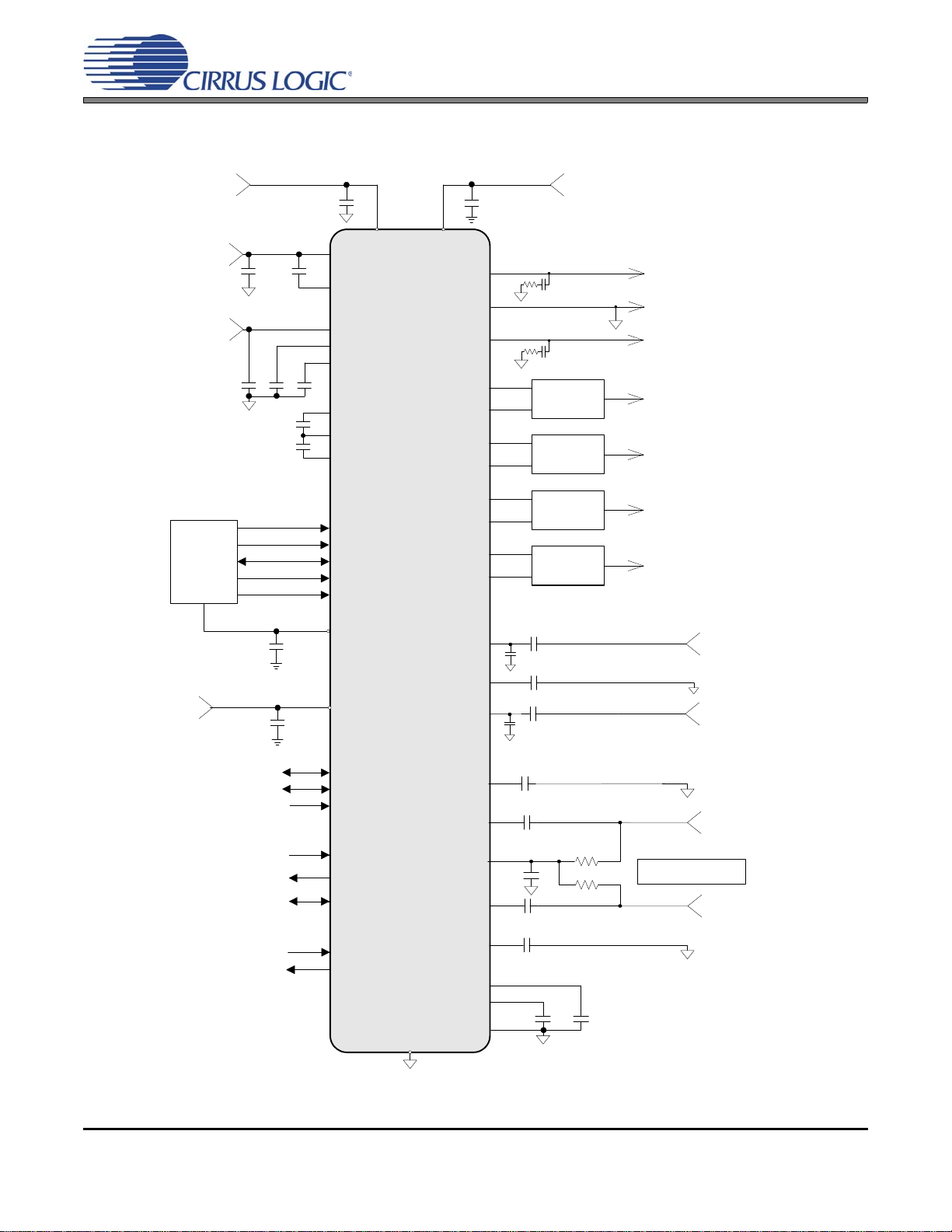
2. TYPICAL CONNECTION DIAGRAMS
1 µF
VREF+
0.1 µF
HP_GND(Thermal Pad)
VL_HD
0.1 µF
+1.5 V to +3.3 V
RESET#
SDI
BITCLK
SYNC
VA
* Capacitors must be C0G or equivalent
MICIN_L+
Differential Mic Left
SDO
CS4207
MICBIAS
HPOUT_L
HPOUT_R
R
L
The value of RL is dictated by
the microphone cartridge.
HD Audio
Bus
Left Headphone
FLYP
VHP_FILT+
2.2 µF
Microphone Bias
1 µF
0.47 µF
10 µF
**
**
** Use low ESR
ceramic capacitors.
LINEOUT_L1+
+Left Line Output 1
LINEOUT_L1-
Right Headphone
LINEOUT_R1+
+Right Line Output 1
LINEOUT_R1-
0.1 µF
33
1 µF
MICIN_L-
1 µF
R
L
Differential Mic Right
1 µF
MICIN_R+
MICIN_R-
LINEOUT_L2+
+Left Line Output 2
LINEOUT_L2-
LINEOUT_R2+
+Right Line Output 2
LINEOUT_R2-
GPIO2
GPIO2
GPIO3
GPIO3
SPDIF_IN
SPDIF_OUT1
S/PDIF TX 1
S/PDIF RX
SENSE_A
SENSE_A
DMIC_SDA1D-Mic In 1
HPREF
0.1 µF
33
Headphone Ground
+5.0 V
Differential to
Single-Ended
Output Filter
Differential to
Single-Ended
Output Filter
Differential to
Single-Ended
Output Filter
Differential to
Single-Ended
Output Filter
VA_HP
2.2 µF
**
FLYN
VHP_FILT-
+1.8 V
0.1 µF
VD
+5.0 V
AGND
10 µF0.1 µF
**
VL_IF
0.1 µF
+3.3 V
FLYC
VCOM
10 µF
‡ Input and Output
filters are optional.
‡
‡
‡
‡
DMIC_SDA2/
SPDIF_OUT2
D-Mic In 2 / S/PDIF TX 2
DMIC_SCL
D-Mic Clk
LINEIN_L+
LINEIN_C-
LINEIN_R+
Left Analog Input
1 µF
1800 pF
*
1 µF
Right Analog Input
1 µF
1800 pF
*
10 µF
VBIAS
+
VA_REF
0.1 µF
+5.0 V
Figure 1. Typical Connection Diagram - Desktop System
*** See Figure 9.
***
CS4207
DS880F4 11
Page 12
CS4207
* Capacitors must be C0G or equivalent
Speaker Driver
2200 pF
560
*
Speaker Driver
2200 pF
560
*
560
560
1 µF
VREF+
0.1 µF
HP_GND(Thermal Pad)
VL_HD
0.1 µF
+1.5 V to +3.3 V
RESET#
SDI
BITCLK
SYNC
VA
MICIN_L+
SDO
CS4207
MICBIAS
HPOUT_L
HPOUT_R
LINEIN_L+
Left Mic In
LINEIN_C-
R
L
The value of RL is dictated by
the microphone cartridge.
HD Audio
Bus
Left Headphone
LINEIN_R+
Right Mic In
FLYP
VHP_FILT+
2.2 µF
Microphone Bias
1 µF
0.47 µF
10 µF
**
**
* *Use low ESR
ceramic capacitors.
LINEOUT_L1+
LINEOUT_L1-
Right Headphone
LINEOUT_R1+
LINEOUT_R1-
0.1 µF
33
MICIN_L-
1 µF
R
L
MICIN_R+
LINEOUT_L2+
LINEOUT_L2-
LINEOUT_R2+
LINEOUT_R2-
GPIO2
GPIO2
GPIO3
GPIO3
SENSE_A
SENSE_A
HPREF
0.1 µF
33
Headphone Ground
+3.3 V
VA_HP
2.2 µF
**
FLYN
VHP_FILT-
+1.8 V
0.1 µF
VD
+3.3 V
AGND
10 µF0.1 µF
**
VL_IF
0.1 µF
+3.3 V
FLYC
VCOM
10 µF
MICIN_R-
Left Analog Input
1 µF
1800 pF
*
1 µF
Right Analog Input
1 µF
1800 pF
*
SPDIF_IN
SPDIF_OUT1
S/PDIF TX 1
S/PDIF RX
DMIC_SDA1
D-Mic In 1
D-Mic In 2 / S/PDIF TX 2
DMIC_SCL
D-Mic Clk
DMIC_SDA2/
SPDIF_OUT2
10 µF
VBIAS
+
VA_REF
0.1 µF
+3.3 V
Figure 2. Typical Connection Diagram - Portable System
*** See Figure 9.
***
12 DS880F4
Page 13
CS4207
3. CHARACTERISTICS AND SPECIFICATIONS
RECOMMENDED OPERATING CONDITIONS
(AGND=DGND=0 V, all voltages with respect to ground.)
Parameters Symbol Min Max Units
DC Power Supply (Note 1)
Analog Core VA 2.97 5.25 V
DAC Reference VA_REF 2.97 5.25 V
Headphone Amplifier VA_HP 2.97 5.25 V
Digital Core VD 1.42 1.89 V
HD Audio Bus Interface VL_HD 1.42 3.47 V
GPIO, S/PDIF and Digital Mic Interface VL_IF 2.97 3.47 V
Ambient Temperature Commercial - CNZ
Automotive - DNZ
T
A
-40
-40
+85
+105
C
C
ABSOLUTE MAXIMUM RATINGS
(AGND = DGND = 0 V; all voltages with respect to ground.)
Parameters Symbol Min Max Units
DC Power Supply Analog Core
DAC Reference
Headphone Amplifier
Digital Core
HD Audio Interface
GPIO, S/PDIF and Digital Mic Interface
Input Current (Note 2) I
Analog Input Voltage (Note 3)
Digital Input Voltage (Note 3) HD Audio Interface
GPIO, S/PDIF and Digital Mic Interface
Ambient Operating T emperature (power applied) T
Storage Temperature T
WARNING: Operation at or beyond these limits may result in permanent damage to the device. Normal operation
is not guaranteed at these extremes.
VA
VA_REF
VA_HP
VD
VL_HD
VL_IF
in
V
IN
V
IND
A
stg
-0.3
-0.3
-0.3
-0.3
-0.3
-0.3
-±10mA
AGND-0.7 VA+0.7
-0.3
-0.3
-55 +115 °C
-65 +150 °C
5.5
5.5
5.5
3.0
4.0
4.0
VL_HD+0.4
VL_IF+0.4
V
V
V
V
V
V
V
V
V
Notes:
1. The device will operate properly over the full range of the analog, digital and interface supplies.
2. Any pin except supplies. Transient currents of up to ±100 mA on the analog input pins will not cause
SCR latch-up.
3. The maximum over/under voltage is limited by the input current.
DS880F4 13
Page 14
CS4207
ANALOG INPUT CHARACTERISTICS (COMMERCIAL - CNZ)
(Test Conditions (unless otherwise specified): Input sine wave (relative to digital full-scale): 1 kHz through passive
input filter; VA_HP = VA; VL_HD = VL_IF = 3.3; VD = 1.8 V; T
20 kHz unless otherwise specified. Sample Frequency = 48 kHz)
= +25C; Measurement Bandwidth is 10 Hz to
A
Parameter
(Note 4)
VA, VA_REF = 5.0 V
(Differential/Single-ended)
Min Typ Max Min Typ Max Unit
VA, VA_R EF = 3.3 V
(Differential/Single-ended)
Line In to PGA to ADC (ADC1 or ADC2; differential perf. characteristics only valid for ADC2)
Dynamic Range
PGA Setting: 0 dB A-weighted
unweighted
PGA Setting: +12 dB A-weighted
unweighted
99/96
96/93
95/86
92/83
105/102
102/99
101/92
98/89
-
-
-
-
95/93
92/90
92/83
89/80
101/99
98/96
98/89
95/86
-
-
-
-
dB
dB
dB
dB
Total Harmonic Distortion + Noise
PGA Setting: 0 dB -1 dBFS
-60 dBFS
-
-
-88/-88
-42/-39
-82/-82
-36/-33
-
-
-95/-92
-38/-36
-89/-86
-32/-30dBdB
PGA Setting: +12 dB -1 dBFS - -88/-88 -82/-82 - -92/-86 -86/-80 dB
Mic In to PGA to ADC (+20 dB) (ADC1 or ADC2; differential perf. characteristics only valid fo r ADC2 )
Dynamic Range
A-weighted
unweighted
86/78
83/75
92/84
89/81
-
-
83/75
80/72
89/81
86/78
-
-
dB
dB
Total Harmonic Distortion + Noise
-1 dBFS - -89/-82 -83/-76 - -86/-78 -80/-72 dB
Other Analog Characteristics
DC Accuracy
Interchannel Gain Mismatch - 0.2 - - 0.2 - dB
Gain Drift - ±100 - - ±100 -
ppm/°C
Offset Error High Pass Filter On - 352 - - 352 - LSB
Interchannel Isolation - 90 - - 90 - dB
HP Amp to Analog Input Isolation
R
= 10 k
L
= 16
R
L
-
-
100
70
-
-
-
-
100
70
-
-
dB
dB
Full-scale Input Voltage - Line In/Mic In
(Differential Inputs)
PGA(0dB) 1.58•VA 1.66•VA 1.74•VA 1.58•VA 1.66•VA 1.74•VA Vpp
Full-scale Input Voltage - Line In
(Single-ended Inputs) PGA (+12dB)
PGA (0dB)
0.79•VA 0.83•VA
0.21•VA
0.87•VA 0.79•VA 0.83•VA
0.21•VA
0.87•VA Vpp
Vpp
Full-scale Input Voltage - Mic In
PGA+Boost(0dB)
(Single-ended Inputs) PGA+Boost(+20dB)
Input Impedance (Note 5)
Mic In (Differential or Pseudo-Diff)
Line In (Pseudo-Diff, PGA = -12/0/+12 dB)
Mic/Line In (Single-Ended, PGA = -12/0/+12 dB)
Common Mode Rejection (Differential Inputs)
0.79•VA 0.83•VA
0.08•VA
-
-
-
43.5
93/99/103
27/33/37
-60--60-dB
0.87•VA 0.79•VA 0.83•VA
0.08•VA
-
-
-
-
-
-
43.5
93/99/103
27/33/37
0.87•VA Vpp
Vpp
-
-
-
k
k
k
14 DS880F4
Page 15
CS4207
ANALOG INPUT CHARACTERISTICS (AUTOMOTIVE - DNZ)
(Test Conditions (unless otherwise specified): Input sine wave (relative to digital full-scale): 1 kHz through passive
input filter; VA_HP = VA; VL_HD = VL_IF = 3.3; VD = 1.8 V; T
to 20 kHz unless otherwise specified. Sample Frequency = 48 kHz)
= -40 to +85C; Measurement Bandwidth is 10 Hz
A
Parameter
(Note 4)
VA, VA_REF = 5.0 V
(Differential/Single-ended)
Min Typ Max Min Typ Max Unit
VA, VA_REF = 3.3 V
(Differential/Single-ended)
Line In to PGA to ADC (ADC1 or ADC2; differential perf. characteristics only valid for ADC2)
Dynamic Range
PGA Setting: 0 dB A-weighted
unweighted
PGA Setting: +12 dB A-weighted
unweighted
99/96
96/93
95/86
92/83
105/102
102/99
101/92
98/89
-
-
-
-
95/93
92/90
92/83
89/80
101/99
98/96
98/89
95/86
-
-
-
-
dB
dB
dB
dB
Total Harmonic Distortion + Noise
PGA Setting: 0 dB -1 dBFS
-60 dBFS
-
-
-88/-88
-42/-39
-82/-82
-36/-33
-
-
-95/-92
-38/-36
-89/-86
-32/-30
dB
dB
PGA Setting: +12 dB -1 dBFS - -88/-88 -82/-82 - -92/-86 -86/-80 dB
Mic In to PGA to ADC (+20 dB) (ADC1 or ADC2; differential perf. characteristics only valid for ADC2)
Dynamic Range
A-weighted
unweighted
86/78
83/75
92/84
89/81
-
-
83/75
80/72
89/81
86/78
-
-
dB
dB
Total Harmonic Distortion + Noise
-1 dBFS - -89/-82 -83/-76 - -86/-78 -80/-72 dB
Other Analog Characteristics
DC Accuracy
Interchannel Gain Mismatch - 0.2 - - 0.2 - dB
Gain Drift - ±100 - - ±100 -
ppm/°C
Offset Error High Pass Filter On - 352 - - 352 - LSB
Interchannel Isolation - 90 - - 90 - dB
HP Amp to Analog Input Isolation
R
= 10 k
L
R
= 16
L
-
-
100
70
-
-
-
-
100
70
-
-
dB
dB
Full-scale Input Voltage - Line In/Mic In
(Differential Inputs)
PGA(0dB) 1.58•VA 1.66•VA 1.74•VA 1.58•VA 1.66•VA 1.74•VA Vpp
Full-scale Input Voltage - Line In
(Single-ended Inputs) PGA(+12dB)
PGA(0dB)
0.79•VA 0.83•VA
0.21•VA
0.87•VA 0.79•VA 0.83•VA
0.21•VA
0.87•VA Vpp
Full-scale Input Voltage - Mic In
PGA+Boost(0dB)
(Single-ended Inputs) PGA+Boost(+20dB)
Input Impedance (Note 5)
Mic In (Differential or Pseudo-Diff)
Line In (Pseudo-Diff, PGA = -12/0/+12 dB)
Mic/Line In (Single-Ended, PGA = -12/0/+12 dB)
0.79•VA 0.83•VA
0.08•VA
-
43.5
93/99/103
27/33/37
0.87•VA 0.79•VA 0.83•VA
0.08•VA
--
43.5
93/99/103
27/33/37
0.87•VA Vpp
-
Common Mode Rejection (Differential Inputs) - 60 - - 60 - dB
4. Referred to the typical full-scale voltage. Applies to all THD+N and Dynamic Range values in the table.
5. Measured between [LINE/MIC]IN_[L/R]+ and [LINE/MIC]IN_[C/L/R]- for differential and pseudo-differential inputs, and between [LINE/MIC]IN_[L/R]+ and AGND for single-ended inputs.
DS880F4 15
Vpp
Vpp
k
k
k
Page 16
CS4207
ADC DIGITAL FILTER CHARACTERISTICS
Parameter (Note 6) Min Typ Max Unit
Passband (Frequency Response) to -0.1 dB corner 0 - .4535 Fs
Passband Ripple -0.09 - 0.17 dB
Stopband 0.6 - - Fs
Stopband Attenuation 70 - - dB
Total Group Delay - 7.6/Fs - s
High-Pass Filter Characteristics
Frequency Response -3.0 dB
Phase Deviation @ 20 Hz - 10 - Deg
Passband Ripple - - 0.17 dB
Filter Settling Time
6. Response is clock dependent and will scale with Fs.
(48 kHz Fs)
-0.13 dB
-
-
-
10
3.6
24.2
5
/Fs
-
-
0s
Hz
Hz
16 DS880F4
Page 17
CS4207
ANALOG OUTPUT CHARACTERISTICS (COMMERCIAL - CNZ)
(Test conditions (unless otherwise specified): Input test signal is a full-scale 997 Hz sine wave; VD = 1.8 V;
VL_HD = VL_IF = 3.3V; T
for the line output and test load R
= +25C; Measurement bandwidth is 10 Hz to 20 kHz; test load RL = 10 k CL= 10 pF
A
= 16 CL = 10 pF for the headphone output (see Figure 3); DAC Gain = 0 dB).
L
Parameter
(Note 4)
VA, VA_REF = 5.0 V
VA_HP = 5.0 V
(Single-ended)
Min Typ Max Min Typ Max Unit
VA, VA_REF = 3.3 V
VA_HP = 3.3 V
(Single-ended)
DAC1; RL = 16 ; DAC Gain = -5 dB
Dynamic Range
18 to 24-Bit A-weighted
unweighted
16-Bit A-weighted
unweighted
95
92
101
98
-
-
93
90
-
-
-
-
93
90
99
96
-
-
93
90
-
-
-
-
dB
dB
dB
dB
Total Harmonic Distortion + Noise
18 to 24-Bit 0 dB
-20 dB
-60 dB
16-Bit 0 dB
-20 dB
-60 dB
DAC1; R
= 10 k
L
-
-
-
-
-
-
-89
-78
-38
-89
-70
-30
-83
-72
-32
-
-
-
-
-
-
-
-
-
-93
-76
-36
-90
-70
-30
-87
-70
-30
-
-
-
dB
dB
dB
dB
dB
dB
Dynamic Range
18 to 24-Bit A-weighted
unweighted
16-Bit A-weighted
unweighted
100
97
-
-
106
103
96
93
-
-
-
-
98
95
104
101
-
-
96
93
-
-
-
-
dB
dB
dB
dB
Total Harmonic Distortion + Noise
18 to 24-Bit 0 dB
-20 dB
-60 dB
16-Bit 0 dB
-20 dB
-60 dB
Other Characteristics for DAC1; R
Full-scale Output Voltage, R
Output Power, THD+N = -75 dB, RL = 16
= 10 k 0.80•VA 0.84•VA 0.88•VA 0.80•VA 0.84•VA 0.88•VA Vpp
L
= 16 or 10 k
L
Output Power, THD+N = 1%, RL = 16 -50- -23-mW
Output Power,THD+N = 10%, RL = 16 -74- -35-mW
Interchannel Isolation (1 kHz) 16
10 k
-
-
-
-
-
-
-38- -17-mW
-
-
-88
-83
-43
-88
-73
-33
80
95
-82
-77
-37
-
-
-
-
-
-
-
-
-
-
-
-
-
-90
-81
-41
-90
-73
-33
80
93
-84
-75
-35
-
-
-
-
-
dB
dB
dB
dB
dB
dB
rms
rms
rms
dB
dB
Interchannel Gain Mismatch - 0.1 0.25 - 0.1 0.25 dB
Output Offset Volt age DAC to HPOUT - 2 4 - 2 4 mV
Gain Drift - ±100 - - ±100 - ppm/°C
AC-Load Resistance (R
Load Capacitance (C
) (Note 7) 16 - - 16 - -
L
) (Note 7) - - 150 - - 150 pF
L
Output Impedance - 300 - - 300 - m
DS880F4 17
Page 18
CS4207
AGND
R
L
C
L
0.1 F
33
HPOUT_L/R
AGND
R
L
C
L
LINEOUT_L/R
Figure 3. Output Test Load, Headphone Out Figure 4. Output Test Load, Line Out
Parameter
(Note 4)
VA, VA_REF = 5.0 V
(Differential/Single-ended)
Min Typ Max Min Typ Max Unit
VA, VA_REF = 3.3 V
(Differential/Single-ended)
DAC2/DAC3; RL = 10 k
Dynamic Range
18 to 24-Bit A-weighted
unweighted
16-Bit A-weighted
unweighted
104/100
101/97
-
-
110/106
107/103
96
93
-
-
-
-
101/97
98/94
-
-
107/103
104/100
96
93
-
-
-
-
dB
dB
dB
dB
Total Harmonic Distortion + Noise
18 to 24-Bit 0 dB
-20 dB
-60 dB
16-Bit 0 dB
-20 dB
-60 dB
Other Characteristics for DAC2/DAC3; R
Full-scale Output Voltage
-
-
-
-
-
-
= 10 k
L
1.60•VA/
0.80•VA
-94/-91
-87/-83
-47/-43
-92
-73
-33
1.68•VA/
0.84•VA
-88/-85
-81/-77
-41/-37
-
-
-
1.76•VA/
0.88•VA
-
-
-
-
-
-
1.60•VA/
0.80•VA
-96/-94
-84/-80
-44/-40
-92
-73
-33
1.68•VA/
0.84•VA
-90/-88
-78/-74
-38/-34
-
-
-
1.76•VA/
0.88•VA
dB
dB
dB
dB
dB
dB
Vpp
Interchannel Isolation (1 kHz) - 100 - - 100 - dB
Interchannel Gain Mismatch - 0.1 0.25 - 0.1 0.25 dB
Gain Drift - ±100 - - ±100 - ppm/°C
AC-Load Resistance (R
Load Capacitance (C
) (Note 7) 3--3--k
L
) (Note 7) --100--100pF
L
Output Impedance - 100 - - 100 -
7. See Figure 3 and Figure 4. RL and CL reflect the recommended minimum resistance and maximum capacitance required for the internal op-amp's stability and signal integrity.
18 DS880F4
Page 19

CS4207
ANALOG OUTPUT CHARACTERISTICS (AUTOMOTIVE - DNZ)
(Test conditions (unless otherwise specified): Input test signal is a full- scale 997 Hz sine wave; VD = 1.8 V ; VL_HD
= VL_IF = 3.3V; T
for the line output and test load R
= -40 to +85C; Measurement bandwidth is 10 Hz to 20 kHz; test load RL = 10 k CL= 10 pF
A
= 16 CL = 10 pF for the headphone output (see Figure 5); DAC Gain = 0 dB).
L
Parameter
(Note 4)
VA, VA_REF = 5.0 V
VA_HP = 5.0 V
(Single-ended)
Min Typ Max Min Typ Max Unit
VA, VA_REF = 3.3 V
VA_HP = 3.3 V
(Single-ended)
DAC1; RL = 16 ; DAC Gain = -5 dB
Dynamic Range
18 to 24-Bit A-weighted
unweighted
16-Bit A-weighted
unweighted
95
92
101
98
-
-
93
90
-
-
-
-
93
90
99
96
-
-
93
90
-
-
-
-
dB
dB
dB
dB
Total Harmonic Distortion + Noise
18 to 24-Bit 0 dB
-20 dB
-60 dB
16-Bit 0 dB
-20 dB
-60 dB
DAC1; R
= 10 k
L
-
-
-
-
-
-
-89
-78
-38
-89
-70
-30
-83
-72
-32
-
-
-
-
-
-
-
-
-
-93
-76
-36
-90
-70
-30
-87
-70
-30
-
-
-
dB
dB
dB
dB
dB
dB
Dynamic Range
18 to 24-Bit A-weighted
unweighted
16-Bit A-weighted
unweighted
100
97
-
-
106
103
96
93
-
-
-
-
98
95
104
101
-
-
96
93
-
-
-
-
dB
dB
dB
dB
Total Harmonic Distortion + Noise
18 to 24-Bit 0 dB
-20 dB
-60 dB
16-Bit 0 dB
-20 dB
-60 dB
Other Characteristics for DAC1; R
Full-scale Output Voltage, R
Output Power, THD+N = -75 dB, RL = 16
= 10 k 0.80•VA 0.84•VA 0.88•VA 0.80•VA 0.84•VA 0.88•VA Vpp
L
= 16 or 10 k
L
Output Power, THD+N = 1%, RL = 16 -50- -23-mW
Output Power,THD+N = 10%, RL = 16 -74- -35-mW
Interchannel Isolation (1 kHz) 16
10 k
-
-
-
-
-
-
-38- -17-mW
-
-
-88
-83
-43
-88
-73
-33
80
95
-82
-77
-37
-
-
-
-
-
-
-
-
-
-
-
-
-
-90
-81
-41
-90
-73
-33
80
93
-84
-75
-35
-
-
-
-
-
dB
dB
dB
dB
dB
dB
rms
rms
rms
dB
dB
Interchannel Gain Mismatch - 0.1 0.25 - 0.1 0.25 dB
Output Offset Volt age DAC to HPOUT - 2 5 - 2 5 mV
Gain Drift - ±100 - - ±100 - ppm/°C
AC-Load Resistance (R
Load Capacitance (C
) (Note 8) 16 - - 16 - -
L
) (Note 8) - - 150 - - 150 pF
L
Output Impedance - 300 - - 300 - m
DS880F4 19
Page 20
CS4207
AGND
R
L
C
L
0.1 F
33
HPOUT_L/R
AGND
R
L
C
L
LINEOUT_L/R
Figure 5. Output Test Load, Headphone Out Figure 6. Output Test Load, Line Out
Parameter
(Note 4)
VA, VA_REF = 5.0 V
(Differential/Single-ended)
Min Typ Max Min Typ Max Unit
VA, VA_REF = 3.3 V
(Differential/Single-ended)
DAC2/DAC3; RL = 10 k
Dynamic Range
18 to 24-Bit A-weighted
unweighted
16-Bit A-weighted
unweighted
104/100
101/97
-
-
110/106
107/103
96
93
-
-
-
-
101/97
98/94
-
-
107/103
104/100
96
93
-
-
-
-
dB
dB
dB
dB
Total Harmonic Distortion + Noise
18 to 24-Bit 0 dB
-20 dB
-60 dB
16-Bit 0 dB
-20 dB
-60 dB
Other Characteristics for DAC2/DAC3; R
Full-scale Output Voltage
-
-
-
-
-
-
= 10 k
L
1.60•VA/
0.80•VA
-94/-91
-87/-83
-47/-43
-92
-73
-33
1.68•VA/
0.84•VA
-88/-85
-81/-77
-41/-37
-
-
-
1.76•VA/
0.88•VA
-
-
-
-
-
-
1.60•VA/
0.80•VA
-96/-94
-84/-80
-44/-40
-92
-73
-33
1.68•VA/
0.84•VA
-88/-88
-78/-74
-38/-34
-
-
-
1.76•VA/
0.88•VA
dB
dB
dB
dB
dB
dB
Vpp
Interchannel Isolation (1 kHz) - 100 - - 100 - dB
Interchannel Gain Mismatch - 0.1 0.25 - 0.1 0.25 dB
Gain Drift - ±100 - - ±100 - ppm/°C
AC-Load Resistance (R
Load Capacitance (C
) (Note 8) 3--3--k
L
) (Note 8) --100--100pF
L
Output Impedance - 100 - - 100 -
8. See Figure 5 and Figure 6. RL and CL reflect the recommended minimum resistance and maximum capacitance required for the internal op-amp's stability and signal integrity.
20 DS880F4
Page 21
CS4207
COMBINED DAC INTERPOLATION & ON-CHIP ANALOG FILTER RESPONSE
Parameter Min Typ Max Unit
Frequency Response 10 Hz to 20 kHz -0.01 - +0.01 dB
Passband to -0.01 dB corner
to -3 dB corner
StopBand - 26256 - Hz
StopBand Attenuation (Note 9) - 102 - dB
Total Group Delay - 0.196 - ms
9. Measurement Bandwidth is from Stopband to 100 kHz.
0
0
-
-
21792
23952
Hz
Hz
DC ELECTRICAL CHARACTERISTICS
(AGND = 0 V; all voltages with respect to ground.)
Parameters Min Typ Max Units
VCOM Characteristics
Nominal Voltage
Output Impedance
DC Current Source/Sink (Note 10)
VHP_FILT+ Characteristics
Nominal Voltage - 0.5•VA_HP - V
VHP_FILT- Characteristics
Nominal Voltage - -0.5•VA_HP - V
MIC BIAS Characteristics
Nominal Voltage VREFE = 000b
VREFE = 001b
VREFE = 010b
VREFE = 100b
DC Current Source (VA=5.0V)
(VA=3.3V)
Power Supply Rejection Ratio (PSRR) (Note 11) 1 kHz - 60 - dB
-
-
-
-
-
-
-
-
-
0.5•VA
23
-
Hi-Z
0.5•VA
GND
0.8•VA
5
3
10
-
-
-
-
-
-
-
-
V
k
A
V
V
V
V
mA
mA
10. The DC current draw represents the allowed current draw from the VCOM pin due to typical leakage
through electrolytic de-coupling capacitors.
11. Valid with the recommended capacitor values on VBIAS. Increasing the capacitance will also increase
the PSRR.
DS880F4 21
Page 22
CS4207
DMIC_SCL
DMIC_SDA
t
h(CLKR-SD)
t
P
t
r
t
f
t
h(CLKF-SD)
t
s(SD-CLKR)
t
s(SD-CLKF)
Right
(B, DATA2)
Channel Data
Left
(A, DATA1)
Channel Data
Left
(A, DATA1)
Channel Data
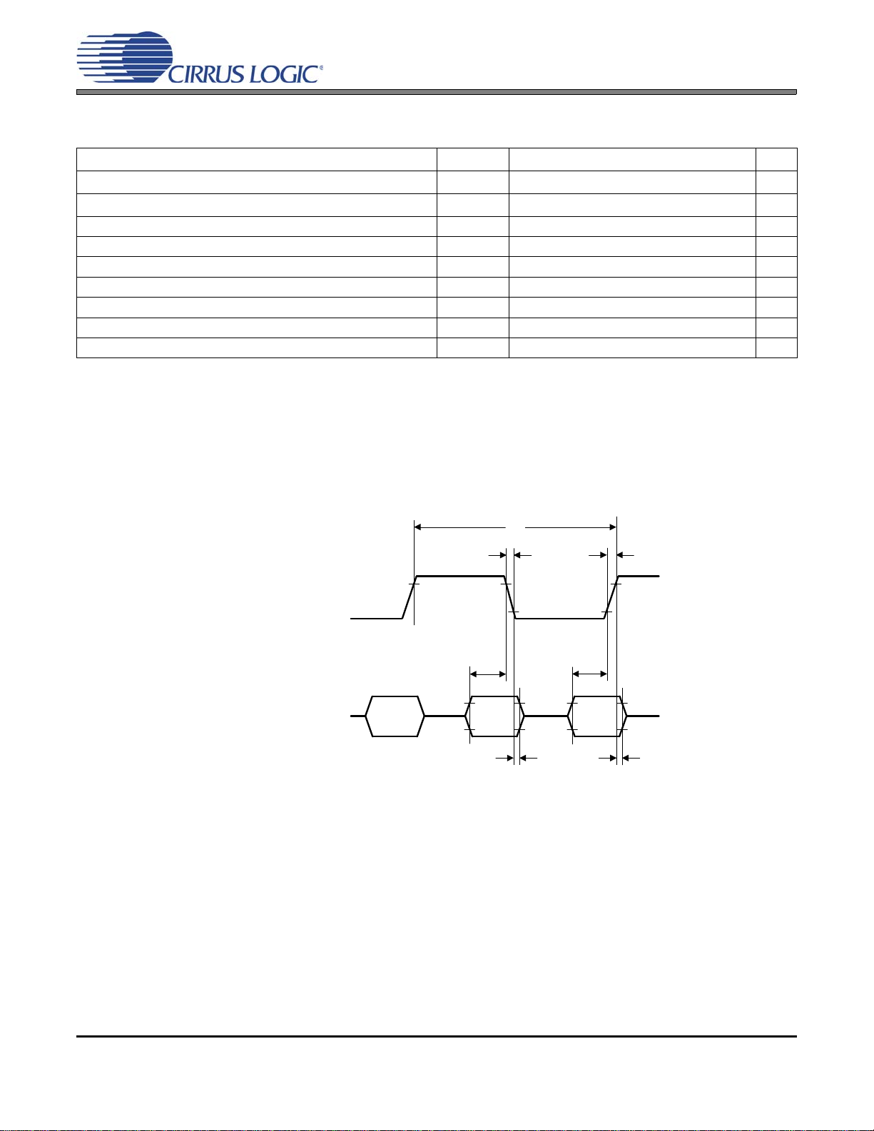
DIGITAL MICROPHONE INTERFACE CHARACTERISTICS
Test conditions: Inputs: Logic 0 = GND = 0 V, Logic 1 = VL_IF; TA = +25 C; C
Parameters Symbol Min Typ Max Units
DMIC_SCL Period (Fs
DMIC_SCL Period (Fs
DMIC_SCL Duty Cycle - 45 - 55 %
DMIC_SCL Rise Time (Note 13) t
DMIC_SCL Fall Time (Note 13) t
DMIC_SDA Setup Time Before DMIC_SCL Rising Edge t
DMIC_SDA Hold Time After DMIC_SCL Rising Edge t
DMIC_SDA Setup Time Before DMIC_SCL Falling Edge t
DMIC_SDA Hold Time After DMIC_SCL Falling Edge t
>= 44.1 kHz) (Note 12)
ADC
<= 32.0 kHz) (Note 12)
ADC
t
P
t
P
r
f
s(SD-CLKR)
h(CLKR-SD)
s(SD-CLKF)
h(CLKF-SD)
Notes:
12. The output clock frequency will follow the Bit Clock (BITCLK) frequency divided by 8 or 12, depending on
the sample rate of the ADC. Any deviation of the Bit Clock source from the nominal supported rates will be
directly imparted to the output clock rate by the same factor (e.g. +100 ppm offset in the frequency of BITCLK will become a +100 ppm offset in DMIC_SCL). For the nominal value of T_cyc reference HDA024-A
(see Note 4 in “References” on page 147).
13. Rise and fall times are measured from 0.1 • VL_IF to 0.9 • VL_IF.
= 30 pF.
LOAD
- 8 • T_cyc
- 12 • T_cyc
- - 10 ns
- - 10 ns
40 - - ns
5--ns
40 - - ns
6--ns
-
-
ns
ns
22 DS880F4
Figure 7. Digital MIC Interface Timing
Page 23

DIGITAL INTERFACE SPECIFICATIONS & CHARACTERISTICS
Parameters (Note 14) Symbol Min Max Units
Input Leakage Current I
Input Pin Capacitance C
VL_HD = 1.5 V
High-Level Input Voltage V
Low-Level Input Voltage V
High-Level Output Voltage (I
Low-Level Output Voltage (I
= -500 A) V
OUT
= 1500 A) V
OUT
VL_HD = 3.3 V
High-Level Input Voltage V
Low-Level Input Voltage V
High-Level Output Voltage (I
Low-Level Output Voltage (I
= -500 A) V
OUT
= 1500 A) V
OUT
VL_IF = 3.3 V
High-Level Input Voltage V
Low-Level Input Voltage V
High-Level Output Voltage (I
Low-Level Output Voltage (I
= -100 A) V
OH
= 100 A) V
OL
in
in
IH
IL
OH
OL
IH
IL
OH
OL
IH
IL
OH
OL
-±10A
-7.5pF
0.60•VL_HD - V
- 0.40•VL_HD V
0.90•VL_HD - V
- 0.10•VL_HD V
0.65•VL_HD - V
- 0.35•VL_HD V
0.90•VL_HD - V
- 0.10•VL_HD V
0.65•VL_IF - V
-0.35•VL_IFV
VL_IF - 0.2 - V
-0.2V
CS4207
14. See “Digital I/O Pin Characteristics” on p 10 for HD Audio I/F and control power rails.
HD AUDIO BUS SPECIFICATIONS & CHARACTERISTICS
Parameter Symbol Min Typ Max Units
BITCLK Period T
BITCLK High Time T
BITCLK Low Time T
CYC
HIGH
LOW
41.163 41.67 42.171 ns
17.50 24.16 ns
17.50 24.16 ns
BITCLK Jitter 150 500 ps
SDI Valid After BITCLK Rising T
SDO Setup Time T
SDO Hold Time T
TCO
SU
H
311ns
5ns
5ns
S/PDIF TRANSMITTER/RECEIVER SPECIFICATIONS & CHARACTERISTICS
Parameter Symbol Min Typ Max Units
Transmitter Specifications & Characteristics
AES3 Transmitter Output Jitter T
Receiver Specifications & Characteristics
PLL Clock Recovery Sample Rate Range f
Input Jitter Tolerance T
JIT(rms)
rec
JIT(rms)
meets IEC 60958-3 ps
kHz
meets IEC 60958-3 ps
DS880F4 23
Page 24
POWER CONSUMPTION
(This table represents the power consumption for individual circuit blocks within the codec) (See ( N o te 15 ))
Typical Current (mA)
CS4207
Individual Block Operation
Codec D3 State- unsolicited
1
response capable (Note 16)
ADC1 or ADC2 with PGA oper-
2
ation and Pseudo-Diff Inputs
DAC1 with Headphone/Line
3
Out (Note 17)
DAC2 or DAC3 with Differen-
4
tial Line Out (Note 18)
S/PDIF transmitter with SRC
5
function
S/PDIF receiver with SRC
6
function
i
VA
VA/
VA_ HP
3.3 0.94 0.00
5.0 1.20 0.00 12.24
3.3 5.47 0.00
5.0 6.23 0.00 44.80
3.3 11.08 1.51
5.0 14.06 1.76 95.12
3.3 10.72 0.00
5.0 13.59 0.00 83.84
3.3 0.84 0.00
5.0 1.10 0.00 22.51
3.3 0.84 0.00
5.0 1.10 0.00 28.64
i
VA_HP
i
VD
VD
=1.8V
3.34 0.07 0.00
7.27 0.17 0.00
8.79 0.06 0.00
8.72 0.06 0.00
8.90 0.07 0.23
12.67 0.10 0.00
i
VL_HD
VL_HD
=3.3V
i
VL_IF
VL_IF
=3.3V
Tota l P ower
for individual
(mW)
block
9.35
31.70
57.57
51.27
19.78
25.91
15. Unless otherwise noted, test conditions are as follows: All zeros input, sample rate = 48 kHz; No load.
16. RESET# held HI, all HDA Bus clocks and data lines are running; HDA Interface running with support
for unsolicited responses; All converters are in D3 state.
17. Full-scale single-ended output signal into a 10 k load.
18. Full-scale differential output signal into a 10 k load.
(The following table demonstrates the total power consumption for typical system operation. These total codec
power numbers are derived from the individual block power consumption numbers in the previous table.)
Power States
Typical Codec
Operation
Stereo Record from Line In
1
1 (PGA/ADC1)
Stereo Playback to Head-
2
phone (No Load)
Stereo Playback to Head-
3
phone Out and S/PDIF Out
Receive from S/PDIF and
4
Playback to S/PDIF Out
Stereo Record & Playback
5
Line In 1 / Line Out 1
ADC1
ADC2
DAC1
DAC2
DAC3
S/PDIF_OUT
D0 D3 D3 D3 D3 D3 D3
D3 D3 D0 D3 D3 D3 D3
D3 D3 D0 D3 D3 D0 D3
D3 D3 D3 D3 D3 D0 D0
D0 D3 D3 D0 D3 D3 D3
VA/
VA_ HP
S/PDIF_IN
3.3
5.0 57.04
3.3
5.0 107.36
3.3
response + DAC1+ S/PDIF OUT
5.0 129.87
3.3
5.0 63.39
3.3
5.0 140.88
Active Blocks
HDA Interface + unsolicited
response + ADC1
HDA Interface + unsolicited
response + DAC1
HDA Interface + unsolicited
HDA Interface + unsolicited
response + S/PDIF IN/OUT
HDA Interface + unsolicited
response + ADC1 + DAC2
Total Codec
Power (mW)
41.04
66.91
86.69
55.04
92.31
24 DS880F4
Page 25

4. CODEC RESET AND INITIALIZATION
4.1 Link Reset
A Link Reset is a system controller generated assertion of the HD Audio Bus RESET# signal. A Link reset
will cause some of the HD Audio bus interface logic to be initialized. Following a Link Reset, the CS4207
will perform the Codec Initialization request sequence. Many of the codec settings will remain unchanged
following a Link Reset. See “Register Settings Across Reset Conditions” section on page 29 for more details.
When the codec has detected a Link Reset condition, all converter widgets and pin widgets will transition to
a low power operating mode, if previously in D0. The actual power states reported will remain unchanged,
i.e. if in D0 or D3 prior to Link Reset, the widget stays in D0 or D3. If enabled, presence detection will continue to sense any impedance changes and issue a power state change request to the Link prior to asserting
an Unsolicited Response.
4.2 Function Group Reset
Because the CS4207 supports the Extended Power State Support (EPSS), a single occurrence of the Func-
tion Group Reset
to the power-on reset values (as descri be d in the HD Aud io Spe cification, Rev. 1.0). Whe n the CS4207 receives a single Function Group Reset verb, the codec will issue a response to the verb to acknowledge receipt, and reset each input/output converter widget’s Stream Number and Lowest Channel Number to the
default (0h). No other settings are modified. See “Register Settings Across Reset Conditions” section on
page 29 for more details.
command will NOT cause the Audio Function unit and all associated widgets to initialize
CS4207
The CS4207 will respond to the newly created “Double Function Group Reset” (as defined in HDA015-B,
March 1, 2007) and will reset most of the register settings to their power on defaults. This “Double Function
Group Reset” will not affect the HD Audio bus interface logic or the unique codec physical address, which
must be reset with the link RESET#
quence on the link. In addition, the Configuration Default settings will not be reset with a “Double Function
Group Reset”.
This new reset condition is created by sending two Function Group resets back to back. The “Double Function Group Reset” is defined as two (2) Function Group Reset verbs received without any other intervening
verbs. The Function Group Reset verbs are not required to be received in sequentia l frames, but there must
not be any other verbs received in frames between the receipt of the Function Group Reset verbs. There
are no implied time outs between the time the first Functio n Group Re set is received an d th e second Function Group Reset verb.
4.3 Codec Initialization
Immediately following the completion of a Link Reset sequence, the CS4207 will initiate a codec initialization
sequence. The purpose of this initialization sequence is to acquire a unique address by which the codec
can thereafter be referenced with Commands on the SDO signal. Durin g th is seq uence, the Contro ller provides the codec with a unique address using its attached SDI signal.
If the CS4207 codec is in a low power D3 state and enabled to support a presence detect event, it will retain
its unique address while in that low power state. If RESET# is de-asserted high, and BITCLK and SYNC are
running at the time of a presence detect event, the codec will signal an unsolicited response.
When put into the D3 low power state and enabled to support a presence detect event, with the link in the
reset state (RESET# is asserted low), the CS4207 will post the occurrence of a wake event and request a
power state change by signaling a power state change request and initialization request. It will reestablish
the connection with the controller by performing a “Codec Initialization request”.
signal. Therefore, the codec will not initiate a Codec Initialization se-
DS880F4 25
Page 26

If RESET# is asserted low, and BITCLK and SYNC are not running at the time (defined as link low power
state), the codec will signal the power state change request and initialization request asynchronously by asserting SDI high continuously until it detects the de-assertion of RESET#. It will then asynchronously drive
SDI low with the de-assertion of the RESET#. With the RESET# signal high, the codec will reestablish the
connection with the controller by performing a “Codec Initialization request”.
4.4 D3 Lower Power State Support
The D3 low power state allows for, but does not require, the lowest possible power consuming state under
software control, in which Extended Po wer States Supported
the D3 state, the CS4207 will retain sufficient operational capability to properly respond to subsequent software Get/Set Power State commands (Verb ID=F05h/705h) to the Audio Function Group (Node ID = 01h).
In addition, while in the D3 power state, Link Reset and “Double Function Group” reset are supported. All
other Get/Set commands will be ignored while the codec is in the D3 power state.
Widgets reporting an EPSS of ‘1’b will transition from D3 state to D0 state in less than 10 ms. This interval
is measured from the response to the Set Power State verb that caused the transition from D3 back to fully
operational D0 state.
It is permissible for the audio fidelity for analog outputs to be slightly degrade d if audio playback begins immediately once the fully operational state is entered. However, audio fidelity will not be degraded 75ms after
the transitioning to D0 state.
CS4207
(EPSS) requirements can be met. While in
4.5 Extended Power States Supported (EPSS)
EPSS indicates that the Audio Function Group or a particular Widget supports additional capabilities allow-
ing better low power operation. The CS4207 will report EPSS support at the Function group level and will
enable low power operation for all Input and Output Converte r Widgets, and the following pin widgets which
are capable of reporting presence detection:
– Headphone pin widget (node ID 09h)
– Line Out 1 pin widget (node ID 0Ah)
– Line In 1/Mic In 2 pin widget (node ID 0Ch)
– Mic In 1/Line In 2 pin widget (node ID 0Dh)
– S/PDIF Receiver Input pin widget (node ID 0Fh).
The following requirements will also be implemented by each input/output converter widget and the above
listed pin widgets:
• Report PowerCntrl set to ‘1’b and support the Supported Power States verb.
• Jack Presence state change reporting (when enabled) will operate regardless of the Widget and Audio
Function Group power state.
• Reporting of presence state change and issuing system wake when the link clock (BITCLK) is not operational is supported.
• The S/PDIF Receiver to S/PDIF Transmitter digital loop-through (no clock re-timing) will continue to operate (if enabled) even thoug h any one, or all of the S/PDIF Receiver In put Converter Widge t, S/PDIF
Transmitter Output Converter Widget or S/PDIF Receiver Input Pin Widget enters into low power states.
This digital loop-through will also continue to operate if the Audio Function Group is placed in the D3 low
power state, during a Link Reset, and even if the HD Audio BITCLK is stopped.
• Dependencies between converter widgets and associated pin widgets will not cause unexpected results
when one node of the dependency is placed into D3 state. The diagrams and tables below demonstrate
typical audio streams.
26 DS880F4
Page 27
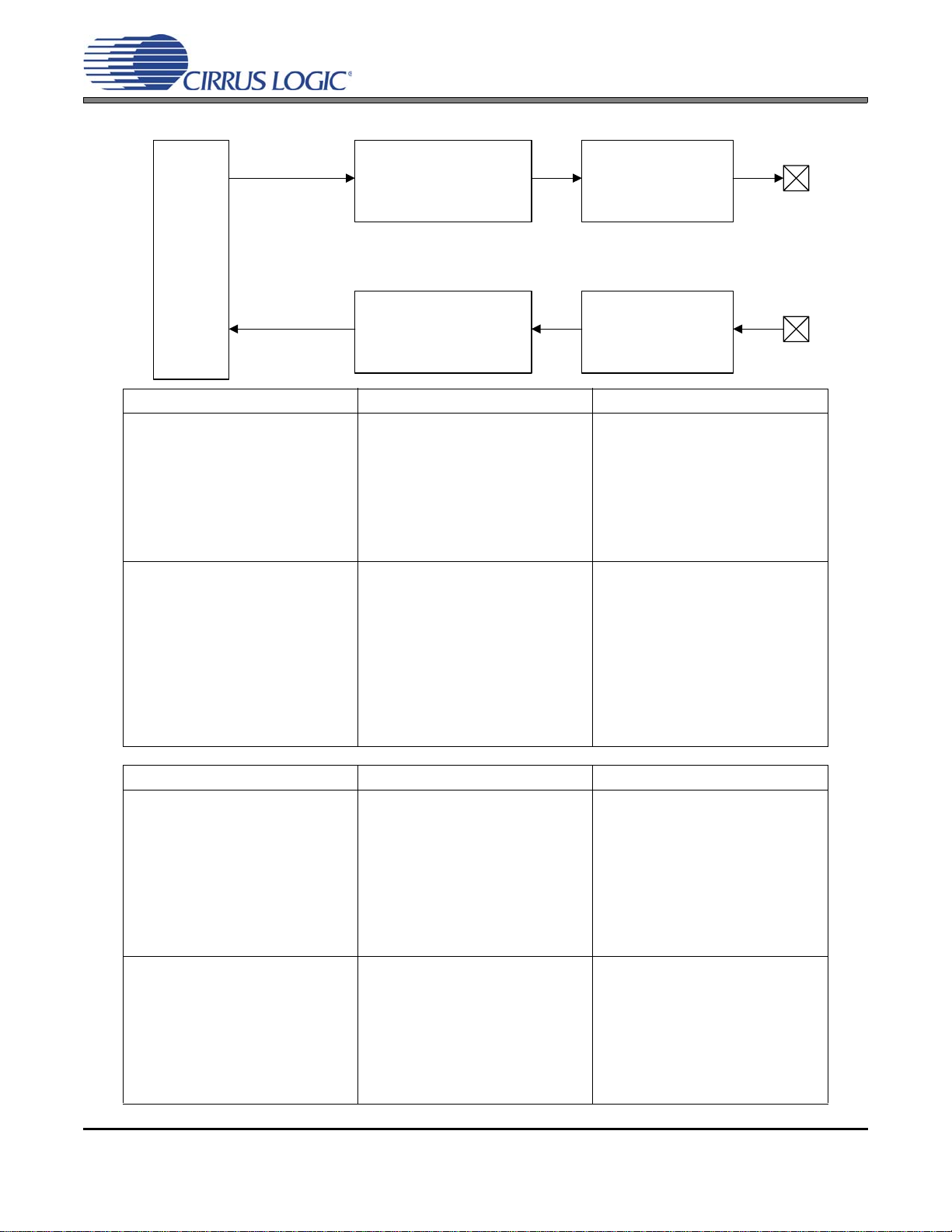
CS4207
LineOut
Output Pin Widget
D0/D3 Power States
DAC
Output Converter Widget
D0/D3 Power States
HD_Audio
Bus
Line In
Input Pin Widget
D0/D3 Power States
ADC
Input Converter Widget
D0/D3 Power States
.
Output Path Output Pin Widget D0 Output Pin Widget D3
• Converter widget continues to
accept audio samples from the
HD Audio bus.
Output Converter Widget D0
Output Converter Widget D3
• Normal Operation in D0
• Converter widget stops accepting audio samples from
the HD Audio bus, sends mute
to the Pin widget and transitions to D3.
• Pin widget outputs a muted
audio signal and supports
presence detect if enabled.
Remains in D0 state.
• Pin widget outputs a muted
audio signal, supports presence detect if enabled and
transitions to D3.
• Converter and Pin Widgets
are in low power D3 state.
Supports presence detect if
enabled.
Input Path Input Pin Widget D0 Input Pin Widget D3
• Converter widget will send
“muted” audio samples to the
HD Audio bus. Remains in D0
state.
Input Converter Widget D0
• Normal Operation in D0
• Pin widget outputs a muted
audio signal, supports presence detect if enabled and
transitions to D3.
• Converter widget stops sending audio samples to the HD
Input Converter Widget D3
Audio bus and transitions to
D3.
• Pin widget shuts down and
supports presence detect if
• Converter and Pin Widgets
are in low power D3 state.
Supports presence detect if
enabled.
enabled. Remains in D0 state.
DS880F4 27
Page 28
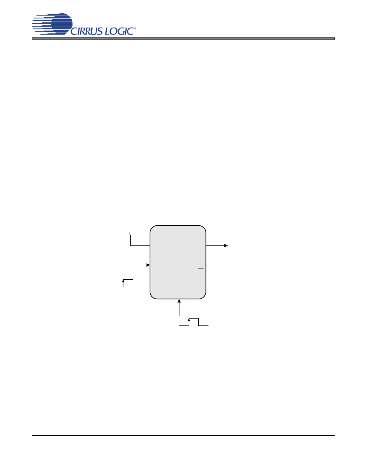
4.6 Power State Settings Reset (PS-SettingsReset)
D
CLR
Q
Q
CLK
‘1’b
Power On Reset or
Double Function
Group Reset
Get “Power State”
Verb
Function Group
PS_Settings Reset Bit
Figure 8. PS-Settings Reset Behavior
PS-SettingsReset is reported as set to on e ‘1’b when, during any low power state transition the settings that
were changed from the defaults (either through software or hardware) have been reset back to their default
state. When these settings have not be en re se t, th is is reported as ‘0’b. The conditions that may reset settings to their defaults are:
1. Power On; always sets the PS-SettingsReset to ‘1’b for all widgets that report EPSS set to ‘1’b and that
have host programmable settings and reset all settings.
2. Double Function Group Reset: sets PS-SettingsReset to ‘1’b for all widgets that report EPSS set to one
‘1’b and that have host programmable settings and resets all settings.
Single Function Group Reset, Link Reset or BITCLK stopped will not cause the PS-SettingsReset bit to be
set to ‘1’b. All settings will persist across these events.
The PS-SettingsReset will be reported at the individual widget level and at the Audio Function Group level.
The PS-SettingsReset bit for the Audio Functio n Group is ha ndled differ ently than at the widget level. For
the Audio Function Group the PS-SettingsReset b it is set to ‘1’b when any widget sets its PS-SettingsReset
to ‘1’b. The Audio Function Group’s PS-SettingsReset bit is the logical “or” of all the PS-SettingsReset bits,
but is latched so that it can be reset independently and not require all the individual widget PS-Settings Reset
bits be reset. This allows a simple poll by the host software to detect when some settings have been reset/changed. For widgets that do not support the EPSS bit, reporting PS-SettingsReset is not required.
If the PS-SettingsReset bit is set to ‘1’b, then this bit for individual widgets will be cleared to ‘0’b on receipt
of any “Set” verb to that widget; or after responding to a “Get” Power State verb to that widget.
CS4207
28 DS880F4
Bit settings within converters and pin widgets that software changed from their defaults will not be changed
by hardware across any Dx state transition, single function group resets or link resets. Table 1 on page 29
outlines how the handling of setting persistence should be performed across Dx states, clock stopping and
resets. Because the CS4207 supports EPSS, the use of PS-SettingsReset to report that settings have been
reset (changed) is required.
Page 29

4.7 Register Settings Across Resets
The CS4207 will perform a complete Power On Reset (POR) initialization if the voltage is cycled from off to
on from the VD pin of the device. All registers will be initialized to the default state. For device behavior due
to other system reset conditions or power state transitions events, see the table below.
Setting Action with
Link Reset
Action with
“Double” Function
Group reset
Action with
“Single” Function
Group reset
CS4207
Action across
D0/D3 state
transitions or link
BITCLK stopped
Unique codec physical address (SDI)
Converter Format;
Type, Base, Mult,
Div, Bits Chan fields
(verb ID = A00/2xx)
Amplifier Gain/Mute
(verb ID = Bxx/3xx)
Connection Select
Control
(verb ID = F01/701)
Power States for the
function group and
individual widgets
(verb ID = F05/705)
Requires codec initialization sequence to
acquire new unique
address.
Persist across Link
Reset.
Index, Mute and Gain
settings persist across
Link Reset.
Persist across Link
Reset.
Power State persist
across Link Reset.
Persist across
“Double” FG reset.
Settings are reset to
POR default value.
PS-SettingsReset set
to ‘1’b.
Settings are reset to
POR default value.
PS-SettingsReset set
to ‘1’b.
Settings are reset to
POR default value.
PS-SettingsReset set
to ‘1’b.
Power State persist
across “Double” FG
reset.
Persist across
“Single” FG reset.
Persist across
“Single” FG reset.
Index, Mute and Gain
settings persist across
“Single” FG reset.
Persist across
“Single” FG reset.
Power State persist
across “Single” FG
reset.
Persist across Dx
state transitions or
BITCLK stopped.
Persist across Dx
state transitions or
BITCLK stopped.
Index, Mute and Gain
settings persist across
Dx state transitions or
BITCLK stopped.
Persist across Dx
state transitions or
BITCLK stopped.
Persist across BITCLK stopped. PS-Act
and PS-Set will be
updated to the current power state
across Dx state transitions.
Converter Stream &
Channel settings
e.g. Stream number
and lowest Channel
number
(verb ID = F06/706)
Pin Widget Controls;
In/Out Enables, Vref
(verb ID = F07/707)
Unsolicited
Response control;
Enable and Tag
(verb ID = F08/708)
Reset to default by
Link reset and does
not set PS-SettingsReset to ‘1’b.
Persist across Link
Reset.
Persist across Link
Reset.
Reset to default by
“Double” FG reset and
does not set PS-SettingsReset to ‘1’b.
Settings are reset to
POR default value.
PS-SettingsReset set
to ‘1’b.
Settings are reset to
POR default value.
PS-SettingsReset set
to ‘1’b.
Reset to default by
“Single” FG reset and
does not set PS-SettingsReset to ‘1’b.
Persist across
“Single” FG reset.
Persist across
“Single” FG reset.
Reset to default
across Dx state transitions and does not set
PS-SettingsReset to
‘1’b.
Persist across Dx
state transitions or
BITCLK stopped.
Persist across Dx
state transitions or
BITCLK stopped.
Table 1. Register Settings Across Reset Conditions
DS880F4 29
Page 30

CS4207
Setting Action with
Link Reset
Pin Sense; Presence
Detect Bit only.
(verb ID = F09/709)
EAPD/BTL enable;
BTL
(verb ID = F0C/70C)
S/PDIF Digital Converter Controls 1 & 2
(verb ID = F0D/70D70E)
GPI/GPO Data,
Enable Mask, Sticky
Masks, Direction
(verb ID = F15F1A/715-71A)
Update to reflect
proper state and save
any Unsolicited
Response that has
not been sent and
send it after first verb
is received.
Persist across Link
Reset.
Persist across Link
Reset.
Persist across Link
Reset.
Action with
“Double” Function
Group reset
Update to reflect
proper state and issue
an Unsolicited
Response if enabled.
Settings are reset to
POR default value.
PS-SettingsReset set
to ‘1’b.
Settings are reset to
POR default value.
PS-SettingsReset set
to ‘1’b.
Settings are reset to
POR default value.
PS-SettingsReset set
to ‘1’b.
Action with
“Single” Function
Group reset
Update to reflect
proper state and issue
an Unsolicited
Response if enabled.
Persist across
“Single” FG reset.
Persist across
“Single” FG reset.
Persist across
“Single” FG reset.
Action across
D0/D3 state
transitions or link
BITCLK stopped
Update to reflect
proper state afte r tr ansition back to full
operation (D0).
Persist across Dx
state transitions or
BITCLK stopped.
Persist across Dx
state transitions or
BITCLK stopped.
Persist across Dx
state transitions or
BITCLK stopped.
Configuration
Default; all 32 bits
(verb ID = F1C/71C71F)
Sub-System ID
(verb ID = F20/720-
723)
Coefficient Index
(verb ID = D/5)
Processing
Coefficient
(verb ID = C/4)
Coefficient
Registers
Digital loop from
S/PDIF Receiver pin
widget to S/PDIF
Transmitter pin widget
Persist across Link
Reset.
Persist across Link
Reset.
Persist across Link
Reset.
Persist across Link
Reset.
Persist across Link
Reset.
Digital Loop persists if
enabled.
Persist across “Double” FG reset.
Persist across “Double” FG reset.
Settings are reset to
POR default value.
Settings are reset to
POR default value.
Settings are reset to
POR default value.
PS-SettingsReset set
to ‘1’b.
Digital Loop persists if
enabled.
Persist across “Single” FG reset.
Persist across
“Single” FG reset.
Persist across
“Single” FG reset.
Persist across
“Single” FG reset.
Persist across
“Single” FG reset.
Digital Loop persists if
enabled.
Persist across Dx
state transitions or
BITCLK stopped.
Persist across Dx
state transitions or
BITCLK stopped.
Persist across Dx
state transitions or
BITCLK stopped.
Persist across Dx
state transitions or
BITCLK stopped.
Persist across Dx
state transitions or
BITCLK stopped.
Digital Loop persists if
enabled.
Table 1. Register Settings Across Reset Conditions
30 DS880F4
Page 31

5. PRESENCE DETECTION
Headphone Out
Left & Right
39.2 k
+/- 1%
nc
To Codec
To Codec
Mic In
Left & Right
nc
To Codec
To Codec
Line In
Left & Right
nc
To Codec
To Codec
Line Out 1
Left & Right
nc
To Codec
To Codec
20.0 k
+/- 1%
10.0 k
+/- 1%
5.1 k
+/- 1%
To Sense_A
2.67 k
+/- 1%
VA
Figure 9. Jack Presence Detect Circuit
5.1 Jack Detection Circuit
The jack detection circuit provides attachment for to up to four pluggable jacks as described in the High Definition Audio Specification. Each jack has an isolated switch (normally open), as shown in Figure 9, which
closes when a plug is inserted into that jack. A “power of two” para llel resistor n etwork is co nnecte d to the
SENSE_A pin as shown. The codec will measure the impedance of this network to determine which jacks
have plugs inserted and set (or clear) the correspon ding “Presence Detect” bit in th e “Pin Sense” control for
that Pin Widget. The jack detect circuitry will remove switch bounce of up to 250-ms duration.
CS4207
5.1.1 Presence Detection and Unsolicited Response
The Pin Widget, if enabled to generate an unsolicited response, will deliver one such response for each
“de-bounced” state change of the “Presence Detect” bit. The “Presence Detect” bit will be stable and readable at the time an unsolicited response is issued. In sensing the insertion or remova l of a jack the codec
will measure the impedance continuously to determine when to report a change of state. Reporting of
state change and change in the presence detect state bits will not occur until any impedance change has
initially stabilized for approximately 250ms. Following this de-bounce period, the codec will report an unsolicited response, if enabled and the HD Audio BITCLK running, within 10ms. If the HD Audio BITCLK is
not running, then the request to wake the Link will occur within 10ms.
Once an unplug or plug event has been signaled to the host via the unsolicited response, another chang e
of the presence detection bits will not be generated unless the jack state has been sensed (de-bounced)
continuously for at least 250ms.
Pin Widgets programmed to generate Unsolicited Responses for Presence Detection state changes will
continue to function in all power states. When generating an Unsolicited Response for a p lug event when
the link is in a low power state (when RESET# is asserted low), sending of an Unsolicited Response will
wait until after the power state change and initialization request and the codec initialization sequence are
complete and the first verb is received to prevent the response from being lost due to software transition
to active power state.
DS880F4 31
Page 32

CS4207
If the codec has detected that the link is entering a Link Reset state (see description below), all Unsolicited
Response requests will be buffered. Once the link is in the Link Reset state, with RESET# asserted low,
the codec will request a power state change and initialization request. Following the codec initialization
cycle where a unique address is provided to the CS4207, the codec will then wait for the first verb to be
received before issuing the Unsolicited Response to prevent the response from being lost due to software
transition to active power state.
The Link Reset entry sequence is defined as follows:
1. The HD Audio Bus controller synchronously completes the current frame but does not signal Frame
Sync (SYNC) during the last eight SDO bit times.
2. The HD Audio Bus controller synchronously asserts RESET# four (or more) BITCLK cycles after the
completion of the current frame.
3. BITCLK is stopped a minimum of four clocks, four rising edges, after the assertion of RESET#.
In the event of a system bus (PCI Bus) reset, the above sequence does not complete, and RESET# is
asynchronously asserted immediately and unconditionally.
When the codec returns to D0 from the D3 lower power state, the state of the presence detection bits will
be correct. If the codec power has been removed, the state of the presence detection bits will be reset to
the default value and the codec
Pin Widget(s). (HDA015-B, March 1, 2007 says that the PS-SettingsReset bit will be set for the affected
Pin widget).
WILL NOT report this by setting the PS-SettingsReset bit for the affected
5.1.2 S/PDIF Receiver Presence Detect
The presence detect scheme for the S/PDIF Receiver will use the logic state transition of the “LOCK” or
“UNLOCK” indicator for the incoming digital stream. The “LOCK” and “UNLOCK” indica tors are sticky bits
(edge-triggered) which indicate the current state of the receiver. These bits are located in the Vendor Processing Widget, see “S/PDIF RX/TX Interface Status (CIR = 0000h)” on p 129. When the S/PDIF Receiver
Input Converter Widget is “enabled” and the “LOCK” indicator is a “1”, then the Presence Detect bit in the
Pin Sense register will be set to ‘1’. The S/PDIF IN Converter Widget (NID=07h) and the S/PDIF Receiver
pin widget (NID=0Fh) must be in the D0 state to support presence detect using this method described.
With an incoming valid S/PDIF signal applied to the SPDIF_IN pin, the “LOCK” status will be valid approximately 200 S/PDIF frames following the receiver being enabled.
32 DS880F4
Page 33

6. HD AUDIO CODEC SUPPORTED VERBS AND RESPONSES
Headphone
Single-Ended
Jack Detect A
D0/D3 Power States
DAC1
PCM;
Vol/Mute;
D0/D3 Power States
02h
HD_Audio
Bus
Line Out 1
SE/Balanced
Jack Detect D
D0/D3 Power States
DAC2
PCM;
Vol/Mute;
D0/D3 Power States
03h
09h
0Ah
Line Out 2
SE/Balanced
(Speaker)
DAC3
PCM;
Vol/Mute;
D0/D3 Power States
04h 0Bh
Line In 1/Mic In 2
SE/Pseudo-Diff; Boost
Jack Detect C
D0/D3 Power States
ADC1
PCM;
Vol/Mute;
D0/D3 Power States
05h 0Ch
Mic In 1/Line In 2
SE/PSD/Bal; Boost
Vref; Jack Detect B
D0/D3 Power States
ADC2
PCM;
Vol/Mute;
D0/D3 Power States
06h 0Dh
Digita l Mic In 1
Boost
0Eh
S/PDIF Receiver
Lock/Unlock Detect
D0/D3 Power States
S/PD IF IN
PCM/Non-PCM;
D0/D3 Power States
07h 0Fh
S/PDIF Transmitter 1
S/PDIF OUT 1
PCM/Non-PCM;
D0/D3 Power States
08h 10h
GPIO
01h
Jack Sense
Processing
Widget
11h
Digita l Mic In 2
Boost
12h
Beep
Generator
13h
S/PDIF Transmitter 2
S/PDIF OUT 2
PCM/Non-PCM;
D0/D3 Power States
14h 15h
6.1 Software Programming Model
CS4207
Figure 10. Software Programming Model
DS880F4 33
Page 34

6.1.1 Node ID Summary
Node ID Description Reference Section
00h Root Node Section 6.2 on page 36
01h Audio Function Group Section 6.3 on page 37
02h DAC1 Output Converter Widget Section 6.4 on page 45
03h DAC2 Output Converter Widget Section 6.4 on page 45
04h DAC3 Output Converter Widget Section 6.4 on page 45
05h ADC1 Input Converter Widget Section 6.5 on page 53
06h ADC2 Input Converter Widget Section 6.5 on page 53
07h S/PDIF Receiver Input Converter Widget Section 6.6 on page 63
08h S/PDIF Transmitter 1 Output Converter Widget Section 6.7 on page 70
09h Headphone Pin Widget Section 6.8 on page 78
0Ah Line Out 1 Pin Widget Section 6.9 on page 85
0Bh Line Out 2 Pin Widget Section 6.10 on page 92
0Ch Line In 1/Mic In 2 Pin Widget Section 6.11 on page 97
0Dh Mic In 1/Line In 2 Pin Widget Section 6.11 on page 97
0Eh Digital Mic 1 In Pin Widget Section 6.12 on page 108
0Fh S/PDIF Receiver Input Pin Widget Section 6.13 on page 114
10h S/PDIF Transmitter 1 Output Pin Widget Section 6.14 on page 120
11h Processing Widget Section 6.15 on page 126
12h Digital Mic 2 In Pin Widget Section 6.12 on page 108
13h Beep Generator Widget Section 6.16 on page 136
14h S/PDIF Transmitter 2 Output Converter Widget Section 6.7 on page 70
15h S/PDIF Transmitter 2 Output Pin Widget Section 6.14 on page 120
CS4207
Table 2. Device Node ID Summary
34 DS880F4
Page 35

6.1.2 Pin Configuration Register Defaults
The Configuration Default Register is required for each Pin Widget. It is used by software as an aid in determining the configuration of jacks and devices attached to the codec. At the time the codec is first powered on, this register is internally loaded with default values, see Table 3, indicating the typical system use
of this particular pin/jack. After this initial loading, the state, including any software writes into the registe r,
will be preserved across reset events. Its state need not be preserved across power level changes.
Port Location Device Type Color Misc Assoc. Sequence
Headphone
Node ID = 09h
(see p83)
Line Out 1
Node ID = 0Ah
(see p91)
Line Out 2
Node ID = 0Bh
(see p96)
Line In 1/Mic In 2
Node ID = 0Ch
(see p104)
Mic In 1/Line In 2
Node ID = 0Dh
(see p105)
Digital Mic In 1
Node ID = 0Eh
(see p110)
S/PDIF In
Node ID = 0Fh
(see p119)
S/PDIF Out 1
Node ID = 10h
(see p124)
Digital Mic In 2
Node ID = 12h
(see p111)
S/PDIF Out 2
Node ID = 15h
(see p125)
Jack
Jack
Fixed Internal Speakers Other Analog Unknown No PDC Override F 0
Jack
Jack
Fixed
Jack
Jack
Fixed
Jack
External/
Front
External/
Rear
External/
Rear
External/
Rear
Other/
Mobile Lid
Inside
External/
Front
External/
Rear
Other/
Mobile Lid
Inside
External/
Rear
Headphone 1/8” Jack Green No PDC Override F 0
Line Out 1/8” Jack Green No PDC Override F 0
Line In 1/8” Jack Blue No PDC Override 5 1
Mic In 1/8” Jack Pink No PDC Override 3 1
Digital In Other Digital Unknown No PDC Override 3 E
S/PDIF In RCA Jack White No PDC Override F 0
S/PDIF Out RCA Jack Orange No PDC Override F 0
Digital In Other Digital Unknown No PDC Override 5 E
S/PDIF Out Optical Jack Black No PDC Override F 0
Table 3. Pin Configuration Register Defaults
CS4207
DS880F4 35
Page 36

6.2 Root Node (Node ID = 00h)
6.2.1 Vendor and Device ID
Get Parameter Command Format:
Bits [31:28] Bits [27:20] Bits [19:8] Bits [7:0]
CAd = X Node ID = 00h Verb ID = F00h Parameter ID = 00h
Response Format:
Bits Type Default Description
31:16 Read Only 1013h
15:0 Read Only 4207h
6.2.2 Revision ID
Get Parameter Command Format:
Bits [31:28] Bits [27:20] Bits [19:8] Bits [7:0]
CAd = X Node ID = 00h Verb ID = F00h Parameter ID = 02h
Response Format:
Bits Type Default Description
31:24 Read Only 00h Re s erved
23:20 Read Only 1h
19:16 Read Only 0h
15:8 Read Only 03h
7:0 Read Only 02h
CS4207
Vendor ID (VID): Cirrus Logic PCI Vendor ID
Device ID (DID): CS4207 Device ID
Major Revision (MAJREV) of the HDA Spec
Minor Revision (MINREV) of the HDA Spec
Revision ID (REVID): This indicates the letter
rev used for all-layer changes.
01h - rev. Ax
02h - rev. Bx
03h - rev. Cx
Stepping ID (SID): This indicates the number
rev used for metal layer changes.
00h - rev. A0 or rev. B0 or rev. C0
01h - rev. A1 or rev. C1
02h - rev. C2
6.2.3 Subordinate Node Count
Get Parameter Command Format:
Bits [31:28] Bits [27:20] Bits [19:8] Bits [7:0]
CAd = X Node ID = 00h Verb ID = F00h Parameter ID = 04h
Response Format:
Bits Type Default Description
31:24 Read Only 00h Re s erved
23:16 Read Only 01h
15:8 Read Only 00h Reserved
7:0 Read Only 01h
36 DS880F4
Starting Node Number (SNN): 1
Total Number of Nodes (TNN): 1
Page 37

6.3 Audio Function Group (Node ID = 01h)
6.3.1 Subordinate Node Count
Get Parameter Command Format:
Bits [31:28] Bits [27:20] Bits [19:8] Bits [7:0]
CAd = X Node ID = 01h Verb ID = F00h Parameter ID = 04h
Response Format:
Bits Type Default Description
31:24 Read Only 00h Reserved
23:16 Read Only 02h
15:8 Read Only 00h Reserved
7:0 Read Only 14h
6.3.2 Function Group Type
Get Parameter Command Format:
Bits [31:28] Bits [27:20] Bits [19:8] Bits [7:0]
CAd = X Node ID = 01h Verb ID = F00h Parameter ID = 05h
CS4207
Starting Node Number (SNN): 2
Total Number of Nodes (TNN): 20
Response Format:
Bits Type Default Description
31:9 Read Only 0 Reserved
8 Read Only 0b
7:0 Read Only 01h
6.3.3 Audio Function Group Capabilities
Get Parameter Command Format:
Bits [31:28] Bits [27:20] Bits [19:8] Bits [7:0]
CAd = X Node ID = 01h Verb ID = F00h Parameter ID = 08h
Response Format:
Bits Type Default Description
31:17 Read Only 0 Reserved
16 Read Only 1b
15:12 Read Only 0h Reserved
11:8 Read Only 9h
7:4 Read Only 0h Reserved
3:0 Read Only Eh
Unsolicited Capable (UC): Unsolicited
Response is not supported on this widget.
Node Type (NT): Audio Function Group
Beep Gen: Beep Generator is present.
Input Delay: represents the number of samples
between when the sample is received as an analog signal at the pin and when the digital representation is transmitted on the High Definition
Audio Link. This may be a “typical” value.
Output Delay: represents the number of sam-
ples between when the sample is received from
the Link and when it appears as an analog signal
at the pin. This may be a “typical” value.
DS880F4 37
Page 38

6.3.4 Supported PCM Size, Rates
Get Parameter Command Format:
Bits [31:28] Bits [27:20] Bits [19:8] Bits [7:0]
CAd = X Node ID = 01h Verb ID = F00h Parameter ID = 0Ah
Response Format:
Bits Type Default Description
31:21 Read Only 00000000000b Reserved
20 Read Only 1b
19 Read Only 1b
18 Read Only 1b
17 Read Only 1b
16 Read Only 0b
15:12 Read Only 0h Reserved
11 Read Only 0b
10 Read Only 1b
9 Read Only 1b
8 Read Only 1b
7 Read Only 1b
6 Read Only 1b
5 Read Only 1b
4 Read Only 1b
3 Read Only 0b
2 Read Only 0b
1 Read Only 0b
0 Read Only 0b
CS4207
32-Bit (32B): 32-bit audio format is supported.
24-Bit (24B): 24-bit audio format is supported.
20-Bit (20B): 20-bit audio format is supported.
16-Bit (16B): 16-bit audio format is supported.
8-Bit (8B): 8-bit audio format is not supported.
Rate-12 (R12): 384 kHz (48*8) rate is not sup-
ported.
Rate-11 (R11): 192.0 kHz (48*4) rate is sup-
ported.
Rate-10 (R10): 176.4 kHz (44.1*4) rate is sup-
ported.
Rate-9 (R9): 96.0 kHz (48*2) rate is supported.
Rate-8 (R8): 88.2 kHz (44.1*2) rate is supported.
Rate-7 (R7): 48.0 kHz rate is supported.
Rate-6 (R6): 44.1 kHz rate is supported.
Rate-5 (R5): 32.0 kHz (48*2/3) rate is supported.
Rate-4 (R4): 22.05 kHz (44.1/2) rate is not sup-
ported.
Rate-3 (R3): 16.0 kHz (48/3) rate is not sup-
ported
Rate-2 (R2): 11.025 kHz (44.1/4) rate is not sup-
ported.
Rate-1 (R1): 8.0 kHz (48/6) rate is not sup-
ported.
38 DS880F4
Page 39

6.3.5 Supported Stream Formats
Get Parameter Command Format:
Bits [31:28] Bits [27:20] Bits [19:8] Bits [7:0]
CAd = X Node ID = 01h Verb ID = F00h Parameter ID = 0Bh
Response Format:
Bits Type Default Description
31:3 Read Only 0 Reserved
2 Read Only 0b
1 Read Only 0b
0 Read Only 1b
6.3.6 Supported Power States
Get Parameter Command Format:
Bits [31:28] Bits [27:20] Bits [19:8] Bits [7:0]
CAd = X Node ID = 01h Verb ID = F00h Parameter ID = 0Fh
CS4207
AC-3 (AC3): AC-3™ data is not supported.
Float32 (FLT32): Float32 formatted data is not
supported on this widget.
Pulse Code Modulation (PCM): PCM formatted
data is supported on this widget.
Response Format:
Bits Type Default Description
31 Read Only 1b
EPSS: Function Group supports extended
power states.
30 Read Only 1b CLKSTOP: Function group supports D3 opera-
tion even if there is no BCLK present on the link.
29 Read Only 0b
28:5 Read Only 000000h Reserved
4 Read Only 0b
3 Read Only 1b
2 Read Only 0b
1 Read Only 0b
0 Read Only 1b
S3D3coldSup: Software should place the codec
in D3hot state when the platform is entering S3
state.
D3coldSup: D3cold operation is not supported.
D3Sup: D3hot operation is supported.
D2Sup: D2 operation is not supported.
D1Sup: D1 operation is not supported.
D0Sup: D0 operation is supported.
CLKSTOP is defin ed only at the Function Group only (not at the widget level) and indicates that the Func-
tion Group and all widgets under it support D3 operation even when there is no BITCLK present on the
Link. The maximum exit time back to fully functional is 10 milliseconds from the time that the clock begins
operation and a codec address cycle has been completed. The CLKSTOP capability extends the required
functionality for D3 support while the link is operational to include:
• Reporting of presence detect state changes, if enabled and supported by the pin widg et, even if the Link
Clock is not running (controller low power state) or is currently in a Link Reset condition.
• Presence state changes occurring during Link Reset will be deferred until after the reset sequence has
completed. Presence state change Unsolicited Responses, if enabled, will not be lost because the Link
Clock stops or if Link Resets are generated before the Unsolicited Response for the state change has
been returned to the host.
DS880F4 39
Page 40

• Reporting of ClkStopOk when stopping of the clock would be permitted. The CLKSTOP is a static capability with ClkStopOk a dynamic reporting. The setting the capability CLKSTOP to one (1) and not allowing the clock to stop by not reporting ClkStopOk is not permissible. Unless there is a condition or
dependency that the host software cannot be made aware of, that would prohib it stopping the clock, the
ClkStopOk shall be reported as set (1). It is expected that host software will poll the ClkStopOk before
stopping the clock if the CLKSTOP is reported at one (1).
6.3.7 GPIO Capabilities
Get Parameter Command Format:
Bits [31:28] Bits [27:20] Bits [19:8] Bits [7:0]
CAd = X Node ID = 01h Verb ID = F00h Parameter ID = 11h
Response Format:
Bits Type Default Description
31 Read Only 0b
30 Read Only 0b
29:24 Read Only 0h Reserved
23:16 Read Only 0h
15:8 Read Only 0h
7:0 Read Only 4h
CS4207
GPIOWake: Does not support wake functionality.
GPIOUnsol: Does not support UR functionality.
NumGPIs: No dedicated GPI pins.
NumGPOs: No dedicated GPO pins.
NumGPIOs: AFG supports 4 GPIO pins.
40 DS880F4
Page 41

6.3.8 Power States
Get Parameter Command Format:
Bits [31:28] Bits [27:20] Bits [19:8] Bits [7:0]
CAd = X Node ID = 01h Verb ID = F05h Payload = 00h
Set Parameter Command Format:
Bits [31:28] Bits [27:20] Bits [19:8] Bits [7:0]
CAd = X Node ID = 01h Verb ID = 705h Payload = xxh
Response Format:
Bits Type Default Description
31:11 Read Only 00000h Reserved
10 Read Only 1b
9 Read Only 1b
8 Read Only 0b
7:4 Read Only 0011b
3:0 Read/Write 0011b
CS4207
Power State Settings Reset (PS-SettingsRe-
set): This bit is set to ‘1’b when, during any type
of reset or low power state transition, the settings
that were changed from the defaults, either by
software or hardware, have been reset back to
their default state. When these settings have not
been reset, this is reported as ‘0’b. This bit is
always a ‘1’b following a POR condition. For
more information, see “Power State Settings
Reset (PS-SettingsReset)” on p 28.
Power State Clock Stop OK (PS-ClkStopOK):
This bit is set to a ‘1’b when the codec is capable
of continuing proper operation even when the
HD Audio Bus BITCLK has been stopped. This
bit is valid for the Audio Function Group node
and not the device widgets.
Power State Error (PS-Error): This bit is not
supported and will always return ‘0’b when read.
The power state requested by software will
always be possible following a reasonable time
required to execute the power state transition.
There are no dependencies unknown to software
between nodes that would inhibit transitioning to
the requested power state.
Power State Actual (PS-Act): This field indi-
cates the actual power state of the referenced
node. The default state is D3.
Power State Set (PS-Set): Writes to these bits
set the Audio Function Group to the Power State
as described below:
PSS = ’0000’b; D0 - Fully on.
PSS = ‘0001’b; D1 - Not Supported
PSS = ‘0010’b; D2 - Not Supported
PSS = ‘0011’b; D3 - Allows for lowest possible
power consumption under software control. See
“D3 Lower Power State Support” on page 26 for
more information.
PSS = ‘0100’b; D4 - Not Supported
PS-Set is a Power State field which defines the current power setting of the referenced node. Since this
node is an Audio Function Group node, the actual power state is this setting. Setting this field to the D3
DS880F4 41
Page 42

state for the Audio Function Group node will force all other nodes with power state control to the D3 state.
If the Power State field for this node is set to D0, then the individual power state for each converter will be
uniquely controlled via the corresponding node Power State field.
PS-Act is a Power State field which indicates the actual power state of the referenced no de. Within the
Audio Function Group node, this field will always be equal to the PS-Set field (modulo the time required
to execute a power state transition).
PS-ClkStopOk is reported as a ‘1’b when the co de c is capable of continuing proper ope ratio n in the ab-
sence of the HD Audio Bus BITCLK. This bit is reported only at the Audio Function Group level and is
reserved at the widget level. After accepting a low power state transition request (D3 state) to the Audio
Function Group Node, the codec will begin ramping down all the audio converters. During this time, the
PS-ClkStopOK bit will be set to ‘0’b to signify that the bus BITCLK can not be stopped. Once all the converters have been ramped down, the codec will update the PS-Act bits to reflect the actual transition to
the D3 state and will then set the PS-ClkStopOk bit to a ‘1’b to report the ability of the codec to operate
correctly while in the low power state with the BITCLK stopped. While in the low power D3 state, and with
the bus BITCLK stopped, the pin widgets of the codec which were enabled to support unsolicited responses will continue to operate.
6.3.9 GPIO Data
Get Parameter Command Format:
Bits [31:28] Bits [27:20] Bits [19:8] Bits [7:0]
CAd = X Node ID = 01h Verb ID = F15h Payload = 00h
CS4207
Set Parameter Command Format:
Bits [31:28] Bits [27:20] Bits [19:8] Bits [7:0]
CAd = X Node ID = 01h Verb ID = 715h Payload = xxh
Response Format:
Bits Type Default Description
31:8 Read Only 000000h Reserved
7:4 Read Only 0h
3:0 Read/Write 0h
GPIO[7:4] Data: Not Supported.
GPIO[3:0] Data: For GPIO programmed as
inputs, this value is read only and is the sensed
value on the corresponding pin. For GPIO programmed as outputs, the value written is driven
onto the corresponding pin.
Note that if the corresponding bit in the GPIO
Enable Mask control is not set, pins configured
as outputs will not drive the associated bit value
(as the pin must be in a Hi-Z state), but the value
returned on a read will still reflect the value that
would be driven if the pin were to be enabled in
the GPIO Enable Mask control.
42 DS880F4
Page 43

6.3.10 GPIO Enable Mask
Get Parameter Command Format:
Bits [31:28] Bits [27:20] Bits [19:8] Bits [7:0]
CAd = X Node ID = 01h Verb ID = F16h Payload = 00h
Set Parameter Command Format:
Bits [31:28] Bits [27:20] Bits [19:8] Bits [7:0]
CAd = X Node ID = 01h Verb ID = 716h Payload = xxh
Response Format:
Bits Type Default Description
31:8 Read Only 000000h Reserved
7:4 Read Only 0h
3:0 Read/Write 0h
CS4207
GPIO[7:4] Enable Mask: Not Supported.
GPIO[3:0] Enable Mask: If the bit associated
with a pin is 0, the pin is disabled, and must be in
a Hi-Z state.
If the bit is a 1, the GPIO pin is enabled and the
pin’s behavior will be determined by the GPIO
Direction control.
6.3.11 GPIO Direction
Get Parameter Command Format:
Bits [31:28] Bits [27:20] Bits [19:8] Bits [7:0]
CAd = X Node ID = 01h Verb ID = F17h Payload = 00h
Set Parameter Command Format:
Bits [31:28] Bits [27:20] Bits [19:8] Bits [7:0]
CAd = X Node ID = 01h Verb ID = 717h Payload = xxh
Response Format:
Bits Type Default Description
31:8 Read Only 000000h Reserved
7:4 Read Only 0h
3:0 Read/Write 0h
6.3.12 GPIO Sticky Mask
Get Parameter Command Format:
Bits [31:28] Bits [27:20] Bits [19:8] Bits [7:0]
CAd = X Node ID = 01h Verb ID = F1Ah Payload = 00h
GPIO[7:4] Direction: Not Supported.
GPIO[3:0] Direction: If a bit is a 0, the associ-
ated GPIO signal is configured as an input.
If the bit is set to a 1, the associated GPIO signal
is configured as an output.
Set Parameter Command Format:
Bits [31:28] Bits [27:20] Bits [19:8] Bits [7:0]
CAd = X Node ID = 01h Verb ID = 71Ah Payload = xxh
DS880F4 43
Page 44

Response Format:
Bits Type Default Description
31:8 Read Only 000000h Reserved
7:4 Read Only 0h
3:0 Read/Write 0h
6.3.13 Implementation Identification
This field provides the Board Implementation ID and Assembly ID of the functional group to software. It is a
Read/Write-Once register; BIOS writes to this field to configure the Board Implementation ID and Assembly ID during
the boot process.
Get Parameter Command Format:
Bits [31:28] Bits [27:20] Bits [19:8] Bits [7:0]
CAd = X Node ID = 01h Verb ID = F20h Payload = 00h
CS4207
GPIO[7:4] Sticky Mask: Not Supported.
GPIO[3:0] Sticky Mask: Defines GPIO Input
Type (0 = Non-Sticky, 1 = Sticky) when a GPIO
pin is configured as an input. GPIO inputs configured as Sticky are cleared by writing a 0 to the
corresponding bit of the GPIO Data Control
The default value for these bits (0h) is all pins
Non-Sticky. Non implemented GPIO pins always
return 0’s. Sticky is defined as Positive-Edge
sensitive, Non-Sticky as Level sensitive.
Set Parameter Command Format:
Bits [31:28] Bits [27:20] Bits [19:8] Bits [7:0]
CAd = X Node ID = 01h Verb ID = 720h Payload = xxh (IID bits [7:0])
CAd = X Node ID = 01h Verb ID = 721h Payload = xxh (IID bits [15:8])
CAd = X Node ID = 01h Verb ID = 722h Payload = xxh (IID bits [23:16])
CAd = X Node ID = 01h Verb ID = 723h Payload = xxh (IID bits [31:24])
Response Format:
Bits Type Default Description
31:16 Read/Write Once 1013h
15:8 Read/Write Once 42h
7:0 Read/Write Once 07h
6.3.14 Function Reset
Function Reset is an “Execute” verb. There is no physical register associated with the Function Reset.
See “Function Group Reset” section on page 25 for more details.
Board Manufacturer Identification (BMID):
Contains the PCI Vendor ID of the board manufacturer. Preset to Cirrus Logic’s PCI Vendor ID.
Board SKU (BSKU): Assigned by the board
manufacturer to identify the specific board
design. Preset to 42h for Cirrus Logic codecs.
Assembly ID (AssyID): Uniquely identifies the
specific board assembly. Preset to 07h for the
CS4207.
Set Parameter Command Format:
Bits [31:28] Bits [27:20] Bits [19:8] Bits [7:0]
CAd = X Node ID = 01h Verb ID = 7FFh Payload = 00h
44 DS880F4
Page 45

6.4 DAC1, DAC2, DAC3 Output Converter Widgets (Node ID = 02h, 03h, 04h)
6.4.1 Audio Widget Capabilities
Get Parameter Command Format:
Bits [31:28] Bits [27:20] Bits [19:8] Bits [7:0]
CAd = X DAC1 Node ID=02h
DAC2 Node ID=03h
DAC3 Node ID=04h
Response Format:
Bits Type Default Description
31:24 Read Only 00h Reserved
23:20 Read Only 0h
19:16 Read Only Dh
15:12 Read Only 0h Reserved
11 Read Only 0b
10 Read Only 1b
9 Read Only 0b
8 Read Only 0b
7 Read Only 0b
6 Read Only 0b
5 Read Only 0b
4 Read Only 1b
3 Read Only 1b
2 Read Only 1b
1 Read Only 0b
0 Read Only 1b
Verb ID = F00h Parameter ID = 09h
Type (TYP): Audio Output Converter Widget
Delay (DLY): Number of sample delays through
the widget.
L-R Swap (LRS): This widget is not capable of
swapping the left and right channels.
Power Control (PC): Power S t ate control is sup-
ported on this widget.
Digital (DIG): Widget is not a digital widget.
Connection List (CL): A connection list is not
present on this widget.
Unsolicited Capable (UC): Unsolicited
Response is not supported on this widget.
Processing Widget (PW): This widget does not
contain “Processing Controls” parameters.
Stripe (STRP): Striping is not supported.
Format Override (FO): This bit is a ‘1’ to indi-
cate that the widget contains format information,
and the “Supported Formats” and “Supported
PCM Bits, Rates” should be queried for the widget’s format capabilities.
Amplifier Parameter Override (APO): This wid-
get contains its own amplifier parameters.
Output Amplifier Present (OAP): Output ampli-
fier is present for this widget.
Input Amplifier Present (IAP): Input amplifier is
not present for this widget.
Stereo (ST): A 1 indicates a stereo widget.
CS4207
DS880F4 45
Page 46

6.4.2 Supported PCM Size, Rates
Get Parameter Command Format:
Bits [31:28] Bits [27:20] Bits [19:8] Bits [7:0]
CAd = X DAC1 Node ID=02h
DAC2 Node ID=03h
DAC3 Node ID=04h
Response Format:
Bits Type Default Description
31:21 Read Only 00000000000b Reserved
20 Read Only 1b
19 Read Only 1b
18 Read Only 1b
17 Read Only 1b
16 Read Only 0b
15:12 Read Only 0h Reserved
11 Read Only 0b
10 Read Only 1b
9 Read Only 1b
8 Read Only 1b
7 Read Only 1b
6 Read Only 1b
5 Read Only 1b
4 Read Only 1b
3 Read Only 0b
2 Read Only 0b
1 Read Only 0b
0 Read Only 0b
CS4207
Verb ID = F00h Parameter ID = 0Ah
32-Bit (32B): 32-bit audio format is supported.
24-Bit (24B): 24-bit audio format is supported.
20-Bit (20B): 20-bit audio format is supported.
16-Bit (16B): 16-bit audio format is supported.
8-Bit (8B): 8-bit audio format is not supported.
Rate-12 (R12): 384 kHz (48*8) rate is not sup-
ported.
Rate-11 (R11): 192.0 kHz (48*4) rate is sup-
ported.
Rate-10 (R10): 176.4 kHz (44.1*4) rate is sup-
ported.
Rate-9 (R9): 96.0 kHz (48*2) rate is supported.
Rate-8 (R8): 88.2 kHz (44.1*2) rate is supported.
Rate-7 (R7): 48.0 kHz rate is supported.
Rate-6 (R6): 44.1 kHz rate is supported.
Rate-5 (R5): 32.0 kHz (48*2/3) rate is supported.
Rate-4 (R4): 22.05 kHz (44.1/2) rate is not sup-
ported.
Rate-3 (R3): 16.0 kHz (48/3) rate is not sup-
ported
Rate-2 (R2): 11.025 kHz (44.1/4) rate is not sup-
ported.
Rate-1 (R1): 8.0 kHz (48/6) rate is not sup-
ported.
6.4.3 Supported Stream Formats
Get Parameter Command Format:
Bits [31:28] Bits [27:20] Bits [19:8] Bits [7:0]
CAd = X DAC1 Node ID=02h
DAC2 Node ID=03h
DAC3 Node ID=04h
46 DS880F4
Verb ID = F00h Parameter ID = 0Bh
Page 47

Response Format:
Bits Type Default Description
31:3 Read Only 0 Reserved
2 Read Only 0b
1 Read Only 0b
0 Read Only 1b
6.4.4 Supported Power States
Get Parameter Command Format:
Bits [31:28] Bits [27:20] Bits [19:8] Bits [7:0]
CAd = X DAC1 Node ID=02h
DAC2 Node ID=03h
DAC3 Node ID=04h
Response Format:
Bits Type Default Description
31 Read Only 1b
30:4 Read Only 0000000h Reserved
3 Read Only 1b
2 Read Only 0b
1 Read Only 0b
0 Read Only 1b
CS4207
AC-3 (AC3): AC-3 data is not supported.
Float32 (FLT32): Float32 formatted data is not
supported on this widget.
Pulse Code Modulation (PCM): PCM formatted
data is supported on this widget.
Verb ID = F00h Parameter ID = 0Fh
EPSS: Converter widget supports extended
power states.
D3Sup: D3hot operation is supported.
D2Sup: D2 operation is not supported.
D1Sup: D1 operation is not supported.
D0Sup: D0 operation is supported.
6.4.5 Output Amplifier Capabilities
Get Parameter Command Format:
Bits [31:28] Bits [27:20] Bits [19:8] Bits [7:0]
CAd = X DAC1 Node ID=02h
DAC2 Node ID=03h
DAC3 Node ID=04h
Response Format:
Bits Type Default Description
31 Read Only 1b
30:23 Read Only 00000000b Reserved
22:16 Read Only 0000001b
15 Read Only 0b Reserved
14:8 Read Only 1111111b
7 Read Only 0b Reserved
6:0 Read Only 1110011b
Verb ID = F00h Parameter ID = 12h
Mute Capable (MC): This widget supports mute.
Step Size (SS): Indicates that the size of each
amplifier’s step gain is 0.5 dB.
Number of Steps (NOS): Indicates there are
128 gain steps; Attenuation range is from +6 dB
to -57.5 dB in 0.5 dB steps.
Offset (OFST): Indicates that if “1110011b” is
programmed into the Amplified Gain Control, it
would result in a gain of 0 dB.
DS880F4 47
Page 48

6.4.6 Power States
Get Parameter Command Format:
Bits [31:28] Bits [27:20] Bits [19:8] Bits [7:0]
CAd = X DAC1 Node ID=02h
Set Parameter Command Format:
Bits [31:28] Bits [27:20] Bits [19:8] Bits [7:0]
CAd = X DAC1 Node ID=02h
Response Format:
Bits Type Default Description
31:11 Read Only 00000h Reserved
10 Read Only 1b
9 Read Only 0b Reserved
8 Read Only 0b
7:4 Read Only 0011b
3:0 Read/Write 0011b
DAC2 Node ID=03h
DAC3 Node ID=04h
DAC2 Node ID=03h
DAC3 Node ID=04h
Verb ID = F05h Payload = 00h
Verb ID = 705h Payload = xxh
Power State Settings Reset (PS-SettingsRe-
This bit is set to ‘1’b when, during any type
set):
of reset or low power state transition, the settings
within this widget that were changed from the
defaults, either by software or hardware, have
been reset back to their default state. When
these settings have not been reset, this is
reported as ‘0’b. This bit is always a ‘1’b following a POR condition. For more information, see
Section 4.6
Power State Error (PS-Error): This bit is not
supported and will always return ‘0’b when read.
Power State Actual (PS-Act): This field indi-
cates the actual power state of the referenced
node. The default state is D3.
Power State Set (PS-Set): Writes to these bits
set the Audio Function Group to the Power State
as described below:
PSS = ’0000’b; D0 - Fully on.
PSS = ‘0001’b; D1 - Not Supported
PSS = ‘0010’b; D2 - Not Supported
PSS = ‘0011’b; D3 - Allows for lowest possible
power consumption under software control. See
Section 4.4 for more information.
PSS = ‘0100’b; D4 - Not Supported
CS4207
PS-Set is a PowerState field which defines the current power setting of the referenced node. Since this
node is of type other than an Audio Function Group no de, the actual power state is a function of both this
setting and the PowerState setting of the Audio Fu nction Group node unde r which this node was enumerated (is controlled).
PS-Act is a PowerState field which indicates the actual power state of this node. Within the Audio Func-
tion Group node, this field will always be equal to the PS-Set field (modulo the time required to execute a
power state transition). Within this type of node, this field will be the lower power consuming state of either
a) the PS-Set field of the currently referenced node or b) the PS-Set field of the Audio Function Group
node under which the currently referenced no de was enum e ra te d (is cont ro lled ).
48 DS880F4
Page 49

6.4.7 Converter Stream, Channel
Get Parameter Command Format:
Bits [31:28] Bits [27:20] Bits [19:8] Bits [7:0]
CAd = X DAC1 Node ID=02h
DAC2 Node ID=03h
DAC3 Node ID=04h
Set Parameter Command Format:
Bits [31:28] Bits [27:20] Bits [19:8] Bits [7:0]
CAd = X DAC1 Node ID=02h
DAC2 Node ID=03h
DAC3 Node ID=04h
Response Format:
Bits Type Default Description
31:8 Read Only 000000h Reserved
7:4 Read/Write 0h
3:0 Read/Write 0h
CS4207
Verb ID = F06h Payload = 00h
Verb ID = 706h Payload = xxh
Stream Number (SN): This field is written by
software to indicate the stream number used by
the Output Converter. “0h” is stream 0, “1h” is
stream 1, etc.
By convention, stream 0 is reserved and unused
so that converter whose stream number has
been reset to “0h” does not unintentionally
decode data not intended for them.
Lowest Channel Number (LCN): This field is
written by software to indicate the lowest channel
used by the Output Converter. The stereo converter will use this LCN value plus 1 for its left
and right channel.
6.4.8 Converter Format
Get Parameter Command Format:
Bits [31:28] Bits [27:20] Bits [19:16] Bits [15:0]
CAd = X DAC1 Node ID=02h
DAC2 Node ID=03h
DAC3 Node ID=04h
Set Parameter Command Format:
Bits [31:28] Bits [27:20] Bits [19:16] Bits [15:0]
CAd = X DAC1 Node ID=02h
DAC2 Node ID=03h
DAC3 Node ID=04h
DS880F4 49
Verb ID = Ah Payload = 0000h
Verb ID = 2h Payload = xxxxh
Page 50

CS4207
Response Format:
Bits [15:0] must be programmed with the same value programmed into the Str eam Descriptor, so that the
data format being transmitted on the link matches what is expected by the consumer of the data.
If the TYPE is set to Non-PCM, the controller pushes data over the link and is not concerned with format-
ting. The base rate, data type, and number of Words (MULT) to send each valid frame are specified to
control the rate at which the non-PCM data is sent.
Bits Type Default Description
31:16 Read Only 0000h Reserved
Stream Type (TYPE): If TYPE is non-zero, the
other bits in the format structure have other
15 Read/Write 0b
14 Read/Write 0b
13:11 Read/Write 000b
10:8 Read/Write 000b
7 Read Only 0b Reserved
6:4 Read/Write 000b
3:0 Read/Write 0000b
meanings.
0: PCM
1: Non-PCM
Sample Base Rate (BASE):
0 = 48 kHz
1 = 44.1 kHz
Sample Base Rate Multiple (MULT):
000 = 48 kHz/44.1 kHz or less
001 = x2 (96 kHz, 88.2 kHz, 32 kHz)
010 = x3 (144 kHz)
011 = x4 (192 kHz, 176.4 kHz)
100-111 =
Sample Base Rate Divisor (DIV):
000 = Divide by 1 (48 kHz, 44.1 kHz)
001 = Divide by 2 (24 kHz, 22.05 kHz)
010 = Divide by 3 (16 kHz, 32 kHz)
011 = Divide by 4 (11.025 kHz)
100 = Divide by 5 (9.6 kHz)
101 = Divide by 6 (8 kHz)
110 = Divide by 7
1 11 = Divi de by 8 (6 kHz)
Bits per Sample (BITS): Bits in each sample:
000 = 8 bits. The data will be packed in memory
in 8-bit containers on 16-bit boundaries.
001 = 16 bits. The data will be packed in memory
in 16-bit containers on 16-bit boundaries.
010 = 20 bits. The data will be packed in memory
in 32-bit containers on 32-bit boundaries.
011 = 24 bits. The data will be packed in memory
in 32-bit containers on 32-bit boundaries.
100 = 32 bits. The data will be packed in memory
in 32-bit containers on 32-bit boundaries.
101-111 =
Number of Channels (CHAN): Number of chan-
nels in each frame of the stream:
0000 = 1
0001 = 2
…
1111 = 16
Reserved
Reserved
50 DS880F4
Page 51

6.4.9 Amplifier Gain/Mute
Get Parameter Command Format:
Bits [31:28] Bits [27:20] Bits [19:16] Bits [15:0]
CAd = X DAC1 Node ID=02h
DAC2 Node ID=03h
DAC3 Node ID=04h
Bits [19:16] = ‘Bh’, where bits [15:0] are defined below:
Bits [15:0] Value Description
15 1b
14 0b ‘0’b
13 xb
12:4 000000000b Reserved
3:0 0000b
CS4207
Verb ID = Bh Payload = xxxxh
Get Output/Input (GOI): This bit controls whether the request is for
the input amplifier or the output amplifier. When ‘1’, the output amplifier
is being requested. When ‘0’, the input amplifier is being requested.
Get Left/Right (GLR): This bit controls whether the request is for the
left channel amplifier or the right channel amplifier. When ‘1’, the left
channel amplifier is being requested. When ‘0’, the right channel amplifier is being requested.
Index (IDX): This field specifies the input index of the amplifier setting
to return if the widget has multiple input amplifiers. It is only applicable
if “Get Output/Input” is ‘0’ which indicates input amplifier is being
requested. This field has no meaning and ignored since the widget
does not have multiple input amplifiers. It should be always ‘0’s.
Response Format:
Bits Type Default Description
31:8 Read Only 000000h Reserved
Amplifier Mute (AM): This bit returns the Mute
setting for the amplifier requested. A 1 indicates
7 Read Only 1b
6:0 Read Only 1 110011b
the amplifier is in the Mute condition. If the amplifier requested does not exist, a ‘0’ will be
returned. Default equals Muted.
Amplifier Gain (AG): This field returns the Gain
setting for the amplifier requested. If the amplifier
requested does not exist, all ‘0’s will be returned
Default equals 0 dB.
Set Parameter Command Format:
Bits [31:28] Bits [27:20] Bits [19:16] Bits [15:0]
CAd = X DAC1 Node ID=02h
DAC2 Node ID=03h
DAC3 Node ID=04h
Verb ID = 3h Payload = xxxxh
DS880F4 51
Page 52

Bits [19:16] = ‘3h’, where bits [15:0] are defined below:
Bits Type Default Description
15 Write Only xb
14 Write Only 0b
13 Write Only xb
12 Write Only xb
11:8 Write Only 0000b
7 Write Only xb
6:0 Write Only xxxxxxxb
CS4207
Set Output Amplifier (SOA): Determines if the
value programmed refers to the output amplifier.
Set to a 1 for the value to be accepted.
Set Input Amplifier (SIA): Determines if the
value programmed refers to the input amplifier.
This bit should always be ‘0’ since an input
amplifier is not present on this widget.
Set Left Amplifier (SLA): Selects the left chan-
nel (channel 0). A 1 indicates that the relevant
amplifier should accept the value being set. If
both bits are set, both amplifiers are set.
Set Right Amplifier (SRA): Selects the right
channel (channel 1). A 1 indicates that the relevant amplifier should accept th e value being set.
If both bits are set, both amplifiers are set.
Index (IDX): This field is used when program-
ming the input amplifiers on Selector Widgets
and Sum Widgets. This field is ignored.
Mute (MUTE): When ‘1’, the Mute is active.
When ‘0’, the Mute is inactive.
Gain (GAIN): Specifies the amplifier gain in dB.
52 DS880F4
Page 53

6.5 ADC1, ADC2 Input Converter Widgets (Node ID = 05h, 06h)
6.5.1 Audio Widget Capabilities
Get Parameter Command Format:
Bits [31:28] Bits [27:20] Bits [19:8] Bits [7:0]
CAd = X ADC1 Node ID=05h
ADC2 Node ID=06h
Response Format:
Bits Type Default Description
31:24 Read Only 00h Reserved
23:20 Read Only 1h
19:16 Read Only 8h
15:12 Read Only 0h Reserved
11 Read Only 0b
10 Read Only 1b
9 Read Only 0b
8 Read Only 1b
7 Read Only 0b
6 Read Only 0b
5 Read Only 0b
4 Read Only 1b
3 Read Only 1b
2 Read Only 0b
1 Read Only 1b
0 Read Only 1b
Verb ID = F00h Parameter ID = 09h
Type (TYP): Audio Input Converter Widget
Delay (DLY): Number of sample delays through
the widget.
L-R Swap (LRS): This widget is not capable of
swapping the left and right channels.
Power Control (PC): Power S t ate control is sup-
ported on this widget.
Digital (DIG): Widget is not a digital widget.
Connection List (CL): A connection list is
present on this widget.
Unsolicited Capable (UC): Unsolicited
Response is not supported on this widget.
Processing Widget (PW): This widget does not
contain “Processing Controls” parameters.
Stripe (STRP): Striping is not supported.
Format Override (FO): This bit is a ‘1’ to indi-
cate that the widget contains format information,
and the “Supported Formats” and “Supported
PCM Bits, Rates” should be queried for the widget’s format capabilities.
Amplifier Parameter Override (APO): This wid-
get contains its own amplifier parameters.
Output Amplifier Present (OAP): Is ‘0’ as it is
irrelevant to this Audio Input Converter widget.
Input Amplifier Present (IAP): Input amplifier is
present for this widget.
Stereo (ST): A 1 indicates a stereo widget.
CS4207
DS880F4 53
Page 54

6.5.2 Supported PCM Size, Rates
Get Parameter Command Format:
Bits [31:28] Bits [27:20] Bits [19:8] Bits [7:0]
CAd = X ADC1 Node ID=05h
ADC2 Node ID=06h
Response Format:
Bits Type Default Description
31:21 Read Only 00000000000b Reserved
20 Read Only 1b
19 Read Only 1b
18 Read Only 1b
17 Read Only 1b
16 Read Only 0b
15:12 Read Only 0h Reserved
11 Read Only 0b
10 Read Only 0b
9 Read Only 0b
8 Read Only 1b
7 Read Only 1b
6 Read Only 1b
5 Read Only 1b
4 Read Only 1b
3 Read Only 0b
2 Read Only 1b
1 Read Only 0b
0 Read Only 1b
CS4207
Verb ID = F00h Parameter ID = 0Ah
32-Bit (32B): 32-bit audio format is supported.
24-Bit (24B): 24-bit audio format is supported.
20-Bit (20B): 20-bit audio format is supported.
16-Bit (16B): 16-bit audio format is supported.
8-Bit (8B): 8-bit audio format is not supported.
Rate-12 (R12): 384 kHz (48*8) rate is not sup-
ported.
Rate-11 (R11): 192.0 kHz (48*4) rate is not sup-
ported.
Rate-10 (R10): 176.4 kHz (44.1*4) rate is not
supported.
Rate-9 (R9): 96.0 kHz (48*2) rate is supported.
Rate-8 (R8): 88.2 kHz (44.1*2) rate is supported.
Rate-7 (R7): 48.0 kHz rate is supported.
Rate-6 (R6): 44.1 kHz rate is supported.
Rate-5 (R5): 32.0 kHz (48*2/3) rate is supported.
Rate-4 (R4): 22.05 kHz (44.1/2) rate is not sup-
ported.
Rate-3 (R3): 16.0 kHz (48/3) rate is supported
Rate-2 (R2): 11.025 kHz (44.1/4) rate is not sup-
ported.
Rate-1 (R1): 8.0 kHz (48/6) rate is supported.
6.5.3 Supported Stream Formats
Get Parameter Command Format:
Bits [31:28] Bits [27:20] Bits [19:8] Bits [7:0]
CAd = X ADC1 Node ID=05h
ADC2 Node ID=06h
Response Format:
Bits Type Default Description
31:3 Read Only 0 Reserved
2 Read Only 0b
1 Read Only 0b
0 Read Only 1b
54 DS880F4
Verb ID = F00h Parameter ID = 0Bh
AC-3 (AC3): AC-3 data is not supported.
Float32 (FLT32): Float32 formatted dat a is not
supported on this widget.
Pulse Code Modulation (PCM): PCM formatted
data is supported on this widget.
Page 55

6.5.4 Input Amplifier Capabilities
Get Parameter Command Format:
Bits [31:28] Bits [27:20] Bits [19:8] Bits [7:0]
CAd = X ADC1 Node ID=05h
ADC2 Node ID=06h
Response Format:
Bits Type Default Description
31 Read Only 1b
30:23 Read Only 00000000b Reserved
22:16 Read Only 0000011b
15 Read Only 0b Reserved
14:8 Read Only 01111 11b
CS4207
Verb ID = F00h Parameter ID = 0Dh
Mute Capable (MC): Supports muting.
Step Size (SS): Indicates that the size of each
amplifier’s step gain is 1.0 dB.
Number of Steps (NOS): There are 64 gain
steps; Gain range is from +12 dB to -51 dB in
1.0 dB steps.
If analog input pin widget is selected as input
source, then the range of +12 dB to -12 dB is from
analog PGA and the range of -13 dB to -51 dB is
digital volume control.
7 Read Only 0b Reserved
6:0 Read Only 0110011b
6.5.5 Connection List Length
Get Parameter Command Format:
Bits [31:28] Bits [27:20] Bits [19:8] Bits [7:0]
CAd = X ADC1 Node ID=05h
ADC2 Node ID=06h
Response Format:
Bits Type Default Description
31:8 Read Only 000000h Reserved
7 Read Only 0b
6:0 Read Only 0000010b
If the digital mic input pin widget is selected as the
input source, then the entire gain range from
+12 dB to -51 dB is digital volume control.
Offset (OFST): Indicates that if “0110011b” is pro-
grammed into the Amplified Gain Control, it would
result in a gain of 0 dB.
Verb ID = F00h Parameter ID = 0Eh
Long Form (LF): Connection list is short form.
Connection List Length (CLL): Two selectable
inputs are possible for this widget.
DS880F4 55
Page 56

6.5.6 Supported Power States
Get Parameter Command Format:
Bits [31:28] Bits [27:20] Bits [19:8] Bits [7:0]
CAd = X ADC1 Node ID=05h
ADC2 Node ID=06h
Response Format:
Bits Type Default Description
31 Read Only 1b
30:4 Read Only 0000000h Reserved
3 Read Only 1b
2 Read Only 0b
1 Read Only 0b
0 Read Only 1b
6.5.7 ADC1 Connection List Entry
Get Parameter Command Format:
Bits [31:28] Bits [27:20] Bits [19:8] Bits [7:0]
CAd = X Node ID = 05h Verb ID = F02h Payload = N = xxh
CS4207
Verb ID = F00h Parameter ID = 0Fh
EPSS: Converter widget supports extended
power states.
D3Sup: D3hot operation is supported.
D2Sup: D2 operation is not supported.
D1Sup: D1 operation is not supported.
D0Sup: D0 operation is supported.
Response Format:
Bits Type Default Description
31:24 Read Only 00h
23:16 Read Only 00h
15:8 Read Only 12h
7:0 Read Only 0Ch
6.5.8 ADC1 Connection Select Control
Get Parameter Command Format:
Bits [31:28] Bits [27:20] Bits [19:8] Bits [7:0]
CAd = X Node ID = 05h Verb ID = F01h Payload = 00h
Set Parameter Command Format:
Bits [31:28] Bits [27:20] Bits [19:8] Bits [7:0]
CAd = X Node ID = 05h Verb ID = 701h Payload = xxh
Connection List Entry (N+3):
Returns 00h for N=00h-03h or N>03h.
Connection List Entry (N+2):
Returns 00h for N=00h-03h or N>03h.
Connection List Entry (N+1):
Returns 12h (Digital Mic In 2) for N=00h-03h.
Returns 00h for N>03h.
Connection List Entry (N):
Returns 0Ch (Line In 1) for N=00h-03h.
Returns 00h for N>03h.
56 DS880F4
Page 57

Response Format:
Bits Type Default Description
31:8 Read Only 000000h Reserved
7:0 Read/Write 00h
6.5.9 ADC2 Connection List Entry
Get Parameter Command Format:
Bits [31:28] Bits [27:20] Bits [19:8] Bits [7:0]
CAd = X Node ID = 06h Verb ID = F02h Payload = N = xxh
Response Format:
Bits Type Default Description
31:24 Read Only 00h
23:16 Read Only 00h
15:8 Read Only 0Eh
7:0 Read Only 0Dh
CS4207
Connection Index Value: For a Get command ,
this field specifies the current connection index.
The field is written by software to indicate the
connection index value to be set.
00h: Line In 1 (NID=0Ch)
01h: Digital Mic In 2 (NID=12h)
Connection List Entry (N+3):
Returns 00h for N=00h-03h or N>03h.
Connection List Entry (N+2):
Returns 00h for N=00h-03h or N>03h.
Connection List Entry (N+1):
Returns 0Eh (Digital Mic In 1) for N=00h-03h.
Returns 00h for N>03h
Connection List Entry (N):
Returns 0Dh (Mic In 1) for N=00h-03h.
Returns 00h for N>03h.
6.5.10 ADC2 Connection Select Control
Get Parameter Command Format:
Bits [31:28] Bits [27:20] Bits [19:8] Bits [7:0]
CAd = X Node ID = 06h Verb ID = F01h Payload = 00h
Set Parameter Command Format:
Bits [31:28] Bits [27:20] Bits [19:8] Bits [7:0]
CAd = X Node ID = 06h Verb ID = 701h Payload = xxh
Response Format:
Bits Type Default Description
31:8 Read Only 000000h Reserved
7:0 Read/Write 00h
Connection Index Value: For a Get command ,
this field specifies the current connection index.
The field is written by software to indicate the
connection index value to be set.
00h: Mic In 1 (NID=0Dh)
01h: Digital Mic In 1 (NID=0Eh)
DS880F4 57
Page 58

6.5.11 Power States
Get Parameter Command Format:
Bits [31:28] Bits [27:20] Bits [19:8] Bits [7:0]
CAd = X ADC1 Node ID=05h
Set Parameter Command Format:
Bits [31:28] Bits [27:20] Bits [19:8] Bits [7:0]
CAd = X ADC1 Node ID=05h
Response Format:
Bits Type Default Description
31:11 Read Only 00000h Reserved
10 Read Only 1b
9 Read Only 0b Reserved
8 Read Only 0b
7:4 Read Only 0011b
3:0 Read/Write 0011b
CS4207
Verb ID = F05h Payload = 00h
ADC2 Node ID=06h
Verb ID = 705h Payload = xxh
ADC2 Node ID=06h
Power State Settings Reset (PS-SettingsRe-
set): This bit is set to ‘1’b when, during any type
of reset or low power state transition, the settings
within this widget that were changed from the
defaults, either by software or hardware, have
been reset back to their default state. When
these settings have not been reset, this is
reported as ‘0’b. This bit is always a ‘1’b following a POR condition. For more information, see
“Power State Settings Reset (PS-SettingsReset)” on p 28
Power State Error (PS-Error): This bit is not
supported and will always return ‘0’b when read.
Power State Actual (PS-Act): This field indi-
cates the actual power state of the referenced
node. The default state is D3.
Power State Set (PS-Set): Writes to these bits
set the Audio Function Group to the Power State
as described below:
PSS = ’0000’b; D0 - Fully on.
PSS = ‘0001’b; D1 - Not Supported
PSS = ‘0010’b; D2 - Not Supported
PSS = ‘0011’b; D3 - Allows for lowest possible
power consumption under software control. See
“D3 Lower Power State Support” on page 26 for
more information.
PSS = ‘0100’b; D4 - Not Supported
PS-Set is a PowerState field which defines the current power setting of the referenced node. Since this
node is of type other than an Audio Function Group no de, the actual power state is a function of both this
setting and the PowerState setting of the Audio Fu nction Group node unde r which this node was enumerated (is controlled).
PS-Act is a PowerState field which indicates the actual power state of this node. Within the Audio Func-
tion Group node, this field will always be equal to the PS-Set field (modulo the time required to execute a
power state transition). Within this type of node, this field will be the lower power consuming state of either
a) the PS-Set field of the currently referenced node or b) the PS-Set field of the Audio Function Group
node under which the currently referenced no de was enum e ra te d (is cont ro lled ).
58 DS880F4
Page 59

6.5.12 Converter Stre am, Channel
Get Parameter Command Format:
Bits [31:28] Bits [27:20] Bits [19:8] Bits [7:0]
CAd = X ADC1 Node ID=05h
ADC2 Node ID=06h
Set Parameter Command Format:
Bits [31:28] Bits [27:20] Bits [19:8] Bits [7:0]
CAd = X ADC1 Node ID=05h
ADC2 Node ID=06h
Response Format:
Bits Type Default Description
31:8 Read Only 000000h Reserved
7:4 Read/Write 0h
3:0 Read/Write 0h
CS4207
Verb ID = F06h Payload = 00h
Verb ID = 706h Payload = xxh
Stream Number (SN): This field is written by
software to indicate the stream number used by
the Input Converter. “0h” is stream 0, “1h” is
stream 1, etc.
By convention, stream 0 is reserved and unused
so that converter whose stream number has
been reset to “0h” does not unintentionally
decode data not intended for them.
Lowest Channel Number (LCN): This field is
written by software to indicate the lowest channel
used by the Input Converter. The stereo converter will use this LCN value plus 1 for its left
and right channel.
6.5.13 Converter Format
Get Parameter Command Format:
Bits [31:28] Bits [27:20] Bits [19:16] Bits [15:0]
CAd = X ADC1 Node ID=05h
ADC2 Node ID=06h
Set Parameter Command Format:
Bits [31:28] Bits [27:20] Bits [19:16] Bits [15:0]
CAd = X ADC1 Node ID=05h
ADC2 Node ID=06h
Response Format:
Bits [15:0] must be programmed by software with the same value programmed into the Stre am Descriptor,
so that the data format being transmitted on the link matches what is expected by the consumer of the
data.
Verb ID = Ah Payload = 0000h
Verb ID = 2h Payload = xxxxh
DS880F4 59
Page 60

CS4207
If the TYPE is set to Non-PCM, the controller pushes data over the link and is not concerned with formatting. The base rate, data type, and number of Words (MULT) to send each valid frame are specified to
control the rate at which the non-PCM data is sent.
Bits Type Default Description
31:16 Read Only 0000h Reserved
Stream Type (TYPE): If TYPE is non-zero, the
other bits in the format structure have other
15 Read/Write 0b
14 Read/Write 0b
13:11 Read/Write 000b
10:8 Read/Write 000b
7 Read Only 0b Reserved
6:4 Read/Write 000b
3:0 Read/Write 0000b
meanings.
0: PCM
1: Non-PCM
Sample Base Rate (BASE):
0 = 48 kHz
1 = 44.1 kHz
Sample Base Rate Multiple (MULT):
000 = 48 kHz/44.1 kHz or less
001 = x2 (96 kHz, 88.2 kHz, 32 kHz)
010 = x3 (144 kHz)
011 = x4 (192 kHz, 176.4 kHz)
100-111 =
Sample Base Rate Divisor (DIV):
000 = Divide by 1 (48 kHz, 44.1 kHz)
001 = Divide by 2 (24 kHz, 22.05 kHz)
010 = Divide by 3 (16 kHz, 32 kHz)
011 = Divide by 4 (11.025 kHz)
100 = Divide by 5 (9.6 kHz)
101 = Divide by 6 (8 kHz)
110 = Divide by 7
1 11 = Divi de by 8 (6 kHz)
Bits per Sample (BITS): Number of bits in each
sample:
000 = 8 bits. The data will be packed in memory
in 8-bit containers on 16-bit boundaries.
001 = 16 bits. The data will be packed in memory
in 16-bit containers on 16-bit boundaries.
010 = 20 bits. The data will be packed in memory
in 32-bit containers on 32-bit boundaries.
011 = 24 bits. The data will be packed in memory
in 32-bit containers on 32-bit boundaries.
100 = 32 bits. The data will be packed in memory
in 32-bit containers on 32-bit boundaries.
101-111 =
Number of Channels (CHAN): Number of chan-
nels in each frame of the stream:
0000 = 1
0001 = 2
…
1111 = 16
Reserved
Reserved
60 DS880F4
Page 61

6.5.14 Amplifier Gain/Mute
Get Parameter Command Format:
Bits [31:28] Bits [27:20] Bits [19:16] Bits [15:0]
CAd = X ADC1 Node ID=05h
ADC2 Node ID=06h
Bits [19:16] = ‘Bh’, where bits [15:0] are defined below:
Bits [15:0] Value Description
15 0b
14 0b ‘0’b
13 xb
12:4 000000000b Reserved
3:0 0000b
CS4207
Verb ID = Bh Payload = xxxxh
Get Output/Input (GOI): Controls whether the request is for the input
amplifier or the output amplifier. When ‘0’, the input amplifier is being
requested. When ‘1’, the output amplifier is being requested.
Get Left/Right (GLR): This bit controls whether the request is for the
left channel amplifier or the right channel amplifier. When ‘1’, the left
channel amplifier is being requested. When ‘0’, the right channel amplifier is being requested.
Index (IDX): This field specifies the input index of the amplifier setting
to return if the widget has multiple input amplifiers. It is only applicable
if “Get Output/Input” is ‘0’ which indicates input amplifier is being
requested. This field has no meaning and ignored since the widget
does not have multiple input amplifiers. It should be always ‘0’s.
Response Format:
Bits Type Default Description
31:8 Read Only 000000h Reserved
Amplifier Mute (AM): This bit returns the Mute
setting for the amplifier requested. A 1 indicates
7 Read Only 1b
6:0 Read Only 0110011b
the amplifier is in the Mute condition. If the amplifier requested does not exist, a ‘0’ will be
returned. Default equals Muted.
Amplifier Gain (AG): This field returns the Gain
setting for the amplifier requested. If the amplifier
requested does not exist, all ‘0’s will be returned
Default equals 0 dB.
Set Parameter Command Format:
Bits [31:28] Bits [27:20] Bits [19:16] Bits [15:0]
CAd = X ADC1 Node ID=05h
ADC2 Node ID=06h
Verb ID = 3h Payload = xxxxh
Bits [19:16] = ‘3h’, where bits [15:0] are defined below:
Bits Type Default Description
15 Write Only 0b
14 Write Only xb
Set Output Amplifier (SOA): Bit is always ‘0’
since an output amplifier is not present.
Set Input Amplifier (SIA): Determines if the
value programmed refers to the input amplifier.
Set to a 1 for the value to be accepted.
DS880F4 61
Page 62

Bits Type Default Description
Set Left Amplifier (SLA): Selects the left chan-
13 Write Only xb
12 Write Only xb
11:8 Write Only 0000b
7 Write Only xb
6:0 Write Only xxxxxxxb
nel (channel 0). A 1 indicates that the relevant
amplifier should accept the value being set. If
both bits are set, both amplifiers are set.
Set Right Amplifier (SRA): Selects the right
channel (channel 1). A 1 indicates that the relevant amplifier should accept th e value being set.
If both bits are set, both amplifiers are set.
Index (IDX): This field is used when program-
ming the input amplifiers on Selector Widgets
and Sum Widgets. This field is ignored.
Mute (MUTE): When ‘1’, the Mute is active.
When ‘0’, the Mute is inactive.
Gain (GAIN): Specifies the amplifier gain in dB.
CS4207
62 DS880F4
Page 63

6.6 S/PDIF Receiver Input Converter Widget (Node ID = 07h)
6.6.1 Audio Widget Capabilities
Get Parameter Command Format:
Bits [31:28] Bits [27:20] Bits [19:8] Bits [7:0]
CAd = X Node ID = 07h Verb ID = F00h Parameter ID = 09h
Response Format:
Bits Type Default Description
31:24 Read Only 00h Reserved
23:20 Read Only 1h
19:16 Read Only 8h
15:12 Read Only 0h Reserved
11 Read Only 0b
10 Read Only 1b
9 Read Only 1b
8 Read Only 1b
7 Read Only 1b
6 Read Only 0b
5 Read Only 0b
4 Read Only 1b
3 Read Only 0b
2 Read Only 0b
1 Read Only 0b
0 Read Only 1b
Type (TYP): Audio Input Converter Widget
Delay (DLY): Number of sample delays through
the widget.
L-R Swap (LRS): This widget is not capable of
swapping the left and right channels.
Power Control (PC): Power S t ate control is sup-
ported on this widget.
Digital (DIG): Widget is a digital widget.
Connection List (CL): A connection list is
present on this widget.
Unsolicited Capable (UC): Unsolicited
Response is supported on this widget.
Processing Widget (PW): This widget does not
contain “Processing Controls” parameters.
Stripe (STRP): Striping is not supported.
Format Override (FO): This bit is a ‘1’ to indi-
cate that the widget contains format information,
and the “Supported Formats” and “Supported
PCM Bits, Rates” should be queried for the widget’s format capabilities.
Amplifier Parameter Override (APO): This wid-
get does not contain amplifier parameters.
Output Amplifier Present (OAP): Output ampli-
fier is not present for this widget.
Input Amplifier Present (IAP): Input amplifier is
not present for this widget.
Stereo (ST): A 1 indicates a stereo widget.
CS4207
DS880F4 63
Page 64

6.6.2 Supported PCM Size, Rates
Get Parameter Command Format:
Bits [31:28] Bits [27:20] Bits [19:8] Bits [7:0]
CAd = X Node ID = 07h Verb ID = F00h Parameter ID = 0Ah
Response Format:
Bits Type Default Description
31:21 Read Only 00000000000b Reserved
20 Read Only 1b
19 Read Only 1b
18 Read Only 1b
17 Read Only 1b
16 Read Only 0b
15:12 Read Only 0h Reserved
11 Read Only 0b
10 Read Only 1b
9 Read Only 0b
8 Read Only 1b
7 Read Only 0b
6 Read Only 1b
5 Read Only 1b
4 Read Only 1b
3 Read Only 0b
2 Read Only 0b
1 Read Only 0b
0 Read Only 0b
CS4207
32-Bit (32B): 32-bit audio format is supported.
24-Bit (24B): 24-bit audio format is supported.
20-Bit (20B): 20-bit audio format is supported.
16-Bit (16B): 16-bit audio format is supported.
8-Bit (8B): 8-bit audio format is not supported.
Rate-12 (R12): 384 kHz (48*8) rate is not sup-
ported.
Rate-11 (R11): 192.0 kHz (48*4) rate is sup-
ported.
Rate-10 (R10): 176.4 kHz (44.1*4) rate is not
supported.
Rate-9 (R9): 96.0 kHz (48*2) rate is supported.
Rate-8 (R8): 88.2 kHz (44.1*2) rate is not sup-
ported.
Rate-7 (R7): 48.0 kHz rate is supported.
Rate-6 (R6): 44.1 kHz rate is supported.
Rate-5 (R5): 32.0 kHz (48*2/3) rate is supported.
Rate-4 (R4): 22.05 kHz (44.1/2) rate is not sup-
ported.
Rate-3 (R3): 16.0 kHz (48/3) rate is not sup-
ported
Rate-2 (R2): 11.025 kHz (44.1/4) rate is not sup-
ported.
Rate-1 (R1): 8.0 kHz (48/6) rate is not sup-
ported.
6.6.3 Supported Stream Formats
Get Parameter Command Format:
Bits [31:28] Bits [27:20] Bits [19:8] Bits [7:0]
CAd = X Node ID = 07h Verb ID = F00h Parameter ID = 0Bh
Response Format:
Bits Type Default Description
31:3 Read Only 0 Reserved
2 Read Only 1b
1 Read Only 0b
0 Read Only 1b
64 DS880F4
AC-3 (AC3): AC-3 data is supported.
Float32 (FLT32): Float32 formatted dat a is not
supported on this widget.
Pulse Code Modulation (PCM): PCM formatted
data is supported on this widget.
Page 65

6.6.4 Connection List Length
Get Parameter Command Format:
Bits [31:28] Bits [27:20] Bits [19:8] Bits [7:0]
CAd = X Node ID = 07h Verb ID = F00h Parameter ID = 0Eh
Response Format:
Bits Type Default Description
31:8 Read Only 000000h Reserved
7 Read Only 0b
6:0 Read Only 0000001b
6.6.5 Supported Power States
Get Parameter Command Format:
Bits [31:28] Bits [27:20] Bits [19:8] Bits [7:0]
CAd = X Node ID = 07h Verb ID = F00h Parameter ID = 0Fh
Response Format:
Bits Type Default Description
31 Read Only 1b
30:4 Read Only 0000000h Reserved
3 Read Only 1b
2 Read Only 0b
1 Read Only 0b
0 Read Only 1b
CS4207
Long Form (LF): Connection list is short form.
Connection List Length (CLL): One hard-wired
input is possible for this widget.
EPSS: Converter widget supports extended
power states.
D3Sup: D3hot operation is supported.
D2Sup: D2 operation is not supported.
D1Sup: D1 operation is not supported.
D0Sup: D0 operation is supported.
6.6.6 Connection List Entry
Get Parameter Command Format:
Bits [31:28] Bits [27:20] Bits [19:8] Bits [7:0]
CAd = X Node ID = 07h Verb ID = F02h Payload = N = xxh
Response Format:
Bits Type Default Description
31:24 Read Only 00h
23:16 Read Only 00h
15:8 Read Only 00h
7:0 Read Only 0Fh
DS880F4 65
Connection List Entry (N+3):
Returns 00h for N=00h-03h or N>03h.
Connection List Entry (N+2):
Returns 00h for N=00h-03h or N>03h.
Connection List Entry (N+1):
Returns 00h for N=00h-03h or N>03h.
Connection List Entry (N):
Returns 0Fh (S/PDIF RX) for N=00h-03h.
Returns 00h for N>03h.
Page 66

6.6.7 Power States
Get Parameter Command Format:
Bits [31:28] Bits [27:20] Bits [19:8] Bits [7:0]
CAd = X Node ID = 07h Verb ID = F05h Payload = 00h
Set Parameter Command Format:
Bits [31:28] Bits [27:20] Bits [19:8] Bits [7:0]
CAd = X Node ID = 07h Verb ID = 705h Payload = xxh
Response Format:
Bits Type Default Description
31:11 Read Only 00000h Reserved
10 Read Only 1b
9 Read Only 0b Reserved
8 Read Only 0b
7:4 Read Only 0011b
3:0 Read/Write 0011b
CS4207
Power State Settings Reset (PS-SettingsRe-
set): This bit is set to ‘1’b when, during any type
of reset or low power state transition, the settings
within this widget that were changed from the
defaults, either by software or hardware, have
been reset back to their default state. When
these settings have not been reset, this is
reported as ‘0’b. This bit is always a ‘1’b following a POR condition. For more information, see
“Power State Settings Reset (PS-SettingsReset)” on p 28
Power State Error (PS-Error): This bit is not
supported and will always return ‘0’b when read.
Power State Actual (PS-Act): This field indi-
cates the actual power state of the referenced
node. The default state is D3.
Power State Set (PS-Set): Writes to these bits
set the Audio Function Group to the Power State
as described below:
PSS = ’0000’b; D0 - Fully on.
PSS = ‘0001’b; D1 - Not Supported
PSS = ‘0010’b; D2 - Not Supported
PSS = ‘0011’b; D3 - Allows for lowest possible
power consumption under software control. See
“D3 Lower Power State Support” on page 26 for
more information.
PSS = ‘0100’b; D4 - Not Supported
PS-Set is a PowerState field which defines the current power setting of the referenced node. Since this
node is of type other than an Audio Function Group no de, the actual power state is a function of both this
setting and the PowerState setting of the Audio Fu nction Group node unde r which this node was enumerated (is controlled).
PS-Act is a PowerState field which indicates the actual power state of this node. Within the Audio Func-
tion Group node, this field will always be equal to the PS-Set field (modulo the time required to execute a
power state transition). Within this type of node, this field will be the lower power consuming state of either
a) the PS-Set field of the currently referenced node or b) the PS-Set field of the Audio Function Group
node under which the currently referenced no de was enum e ra te d (is cont ro lled ).
66 DS880F4
Page 67

6.6.8 Converter Stream, Channel
Get Parameter Command Format:
Bits [31:28] Bits [27:20] Bits [19:8] Bits [7:0]
CAd = X Node ID = 07h Verb ID = F06h Payload = 00h
Set Parameter Command Format:
Bits [31:28] Bits [27:20] Bits [19:8] Bits [7:0]
CAd = X Node ID = 07h Verb ID = 706h Payload = xxh
Response Format:
Bits Type Default Description
31:8 Read Only 000000h Reserved
7:4 Read/Write 0h
3:0 Read/Write 0h
CS4207
Stream Number (SN): Indicates the stream
number used by the Input Converter. “0h” is
stream 0, “1h” is stream 1, etc.
By convention, stream 0 is reserved and unused
so that converter whose stream number has
been reset to “0h” does not unintentionally
decode data not intended for them.
Lowest Channel Number (LCN): Indicates the
lowest channel used by the Input Converter. The
stereo converter will use this LCN value plus 1
for its left and right channel.
6.6.9 Converter Format
Get Parameter Command Format:
Bits [31:28] Bits [27:20] Bits [19:16] Bits [15:0]
CAd = X Node ID = 07h Verb ID = Ah Payload = 0000h
Set Parameter Command Format:
Bits [31:28] Bits [27:20] Bits [19:16] Bits [15:0]
CAd = X Node ID = 07h Verb ID = 2h Payload = xxxxh
Response Format:
Bits [15:0] must be programmed by software with the same value programmed into the Stre am Descriptor,
so that the data format being transmitted on the link matches what is expected by the consumer of the
data.
If the TYPE is set to Non-PCM, the controller pushes data over the link and is not concerne d with formatting. The base rate, data type, and number of Words (MULT) to send each valid frame are specified to
control the rate at which the non-PCM data is sent.
Bits Type Default Description
31:16 Read Only 0000h Reserved
15 Read/Write 0b
Stream Type (TYPE): If TYPE is non-zero, the
other bits in the format structure have other
meanings.
0: PCM
1: Non-PCM
DS880F4 67
Page 68

Bits Type Default Description
Sample Base Rate (BASE):
14 Read/Write 0b
13:11 Read/Write 000b
10:8 Read/Write 000b
7 Read Only 0b Reserved
6:4 Read/Write 000b
3:0 Read/Write 0000b
0 = 48 kHz
1 = 44.1 kHz
Sample Base Rate Multiple (MULT):
000 = 48 kHz/44.1 kHz or less
001 = x2 (96 kHz, 88.2 kHz, 32 kHz)
010 = x3 (144 kHz)
011 = x4 (192 kHz, 176.4 kHz)
100-111 =
Sample Base Rate Divisor (DIV):
000 = Divide by 1 (48 kHz, 44.1 kHz)
001 = Divide by 2 (24 kHz, 22.05 kHz)
010 = Divide by 3 (16 kHz, 32 kHz)
011 = Divide by 4 (11.025 kHz)
100 = Divide by 5 (9.6 kHz)
101 = Divide by 6 (8 kHz)
110 = Divide by 7
1 11 = Divi de by 8 (6 kHz)
Bits per Sample (BITS): Number of bits in each
sample:
000 = 8 bits. The data will be packed in memory
in 8-bit containers on 16-bit boundaries.
001 = 16 bits. The data will be packed in memory
in 16-bit containers on 16-bit boundaries.
010 = 20 bits. The data will be packed in memory
in 32-bit containers on 32-bit boundaries.
011 = 24 bits. The data will be packed in memory
in 32-bit containers on 32-bit boundaries.
100 = 32 bits. The data will be packed in memory
in 32-bit containers on 32-bit boundaries.
101-111 =
Number of Channels (CHAN): Number of chan-
nels in each frame of the stream:
0000 = 1
0001 = 2
…
1111 = 16
Reserved
Reserved
CS4207
68 DS880F4
Page 69

6.6.10 Digital Converter Control
Get Parameter Command Format:
Bits [31:28] Bits [27:20] Bits [19:8] Bits [7:0]
CAd = X Node ID = 07h Verb ID = F0Dh/** Payload = 00h
** Note: Address F0Eh is not supported.
Set Parameter Command Format:
Bits [31:28] Bits [27:20] Bits [19:8] Bits [7:0]
CAd = X
CAd = X
Response Format:
The S/PDIF IEC Control (SIC) bits are supported in one of two ways. In the first case referred to as “Codec
Formatted SPDIF,” on an input PCM stream of less than 32 bits, the codec strips off the SIC bits before
transferring the samples to the system and puts them in the Digital Converter Control for later software
access.
In the second case, referred to as “Software Formatted (or Raw) SPDIF,” on a 32-bit input stream, the
entire stream is transferred into the system without the code c stripping any bits. However, the codec mu st
properly interpret the Sync Preamble bits of the stream and then send the appro priately coded preamb le.
The IEC 60958 specification, Section 4.3, “Preambles,” defines the prea mbles and the co ding to be used.
Software will specify the “B,” “M,” or “W” (also known as “X,” “Y,” or “Z”) preambles by encoding the last
four bits of the preamble into the Sync Preamble section (bits 0-3) of the frame. The co dec must examine
the bits specified and encode the proper preamble based on the previous state. The previous state is to
be maintained by the codec hardware.
Bits Type Default Description
31:16 Read Only 0000h Reserved
15 Read Only 0b Reserved
14:8 Read Only 0000000b
7 Read Only 0b
6 Read Only 0b
5 Read Only 0b
4 Read Only 1b
3 Read Only 1b
2 Read Only 0b
1 Read Only 0b
0 Read/Write 0b
Node ID = 07h
Node ID = 07h
CS4207
Verb ID = 70Dh Payload = xxh (SIC bits [7:0])
Verb ID = 70Eh Payload = xxh (SIC bits [15:8])
CC[6:0] (Category Code): Programmed accord-
ing to IEC standards, or as appropriate.
L (Generation Level): Programmed according to
IEC standards, or as appropriate.
PRO (Professional): 1 indicates Professional use
of channel status; 0 indicates Consumer.
/AUDIO (Non-Audio): 1 indicates data is non-
PCM format; 0 indicates data is PCM.
COPY (Copyright): 1 indicates copyright is
asserted; 0 indicates copyright is not asserted.
PRE (Pre-emphasis): 1 indicates filter pre-
emphasis is 50/15 us; 0 pre-emphasis is none.
VCFG (Validity Config.): This bit is only defined
for Output Converters and is Reserved, with a
Read Only value of 0 for Input Converters.
V (Validity): This bit reflects the “Validity flag,”
transmitted in each subframe.
DigEn (Digital Enable): Enables or disables digi-
tal transmission. A 1 indicates that the digital
data can pass through the node. A 0 indicates
that the digital data is blocked from passing
through the node, regardless of the state.
DS880F4 69
Page 70

CS4207
6.7 S/PDIF Transmitter 1, S/PDIF Transmitter 2 Output Converter Widgets (Node ID = 08h, 14h)
6.7.1 Audio Widget Capabilities
Get Parameter Command Format:
Bits [31:28] Bits [27:20] Bits [19:8] Bits [7:0]
CAd = X
Response Format:
Bits Type Default Description
31:24 Read Only 00h Re s erved
23:20 Read Only 0h
19:16 Read Only 4h
15:12 Read Only 0h Reserved
11 Read Only 0b
10 Read Only 1b
9 Read Only 1b
8 Read Only 0b
7 Read Only 0b
6 Read Only 0b
5 Read Only 0b
4 Read Only 1b
3 Read Only 0b
2 Read Only 0b
1 Read Only 0b
0 Read Only 1b
S/P Tx 1 Node ID=08h
S/P Tx 2 Node ID=14h
Verb ID = F00h Parameter ID = 09h
Type (TYP): Audio Output Converter Widget
Delay (DLY): Number of sample delays through
the widget.
L-R Swap (LRS): This widget is not capable of
swapping the left and right channels.
Power Control (PC): Power State control is sup-
ported on this widget.
Digital (DIG): Widget is a digital widget.
Connection List (CL): A connection list is not
present on this widget.
Unsolicited Capable (UC): Unsolicited
Response is not supported on this widget.
Processing Widget (PW): This widget does not
contain “Processing Controls” parameters.
Stripe (STRP): Striping is not supported.
Format Override (FO): This bit is a ‘1’ to indi-
cate that the widget contains format information,
and the “Supported Formats” and “Supported
PCM Bits, Rates” should be queried for the widget’s format capabilities.
Amplifier Parameter Override (APO): This wid-
get does not contain amplifier parameters.
Output Amplifier Present (OAP): Output ampli-
fier is not present for this widget.
Input Amplifier Present (IAP): Input amplifier is
not present for this widget.
Stereo (ST): A 1 indicates a stereo widget.
70 DS880F4
Page 71

6.7.2 Supported PCM Size, Rates
Get Parameter Command Format:
Bits [31:28] Bits [27:20] Bits [19:8] Bits [7:0]
CAd = X
Response Format:
Bits Type Default Description
31:21 Read Only 00000000000b Reserved
20 Read Only 1b
19 Read Only 1b
18 Read Only 1b
17 Read Only 1b
16 Read Only 0b
15:12 Read Only 0h Reserved
11 Read Only 0b
10 Read Only 1b
9 Read Only 1b
8 Read Only 1b
7 Read Only 1b
6 Read Only 1b
5 Read Only 1b
4 Read Only 1b
3 Read Only 0b
2 Read Only 0b
1 Read Only 0b
0 Read Only 0b
S/P Tx 1 Node ID=08h
S/P Tx 2 Node ID=14h
CS4207
Verb ID = F00h Parameter ID = 0Ah
32-Bit (32B): 32-bit audio format is supported.
24-Bit (24B): 24-bit audio format is supported.
20-Bit (20B): 20-bit audio format is supported.
16-Bit (16B): 16-bit audio format is supported.
8-Bit (8B): 8-bit audio format is not supported.
Rate-12 (R12): 384 kHz (48*8) rate is not sup-
ported.
Rate-11 (R11): 192.0 kHz (48*4) rate is sup-
ported.
Rate-10 (R10): 176.4 kHz (44.1*4) rate is sup-
ported.
Rate-9 (R9): 96.0 kHz (48*2) rate is supported.
Rate-8 (R8): 88.2 kHz (44.1*2) rate is supported.
Rate-7 (R7): 48.0 kHz rate is supported.
Rate-6 (R6): 44.1 kHz rate is supported.
Rate-5 (R5): 32.0 kHz (48*2/3) rate is supported.
Rate-4 (R4): 22.05 kHz (44.1/2) rate is not sup-
ported.
Rate-3 (R3): 16.0 kHz (48/3) rate is not sup-
ported
Rate-2 (R2): 11.025 kHz (44.1/4) rate is not sup-
ported.
Rate-1 (R1): 8.0 kHz (48/6) rate is not sup-
ported.
DS880F4 71
Page 72

6.7.3 Supported Stream Formats
Get Parameter Command Format:
Bits [31:28] Bits [27:20] Bits [19:8] Bits [7:0]
CAd = X
S/P Tx 1 Node ID=08h
S/P Tx 2 Node ID=14h
Response Format:
Bits Type Default Description
31:3 Read Only 0 Reserved
2 Read Only 1b
1 Read Only 0b
0 Read Only 1b
6.7.4 Supported Power States
Get Parameter Command Format:
Bits [31:28] Bits [27:20] Bits [19:8] Bits [7:0]
CAd = X
S/P Tx 1 Node ID=08h
S/P Tx 2 Node ID=14h
CS4207
Verb ID = F00h Parameter ID = 0Bh
AC-3 (AC3): AC-3 data is supported.
Float32 (FLT32): Float32 formatted dat a is not
supported on this widget.
Pulse Code Modulation (PCM): PCM formatted
data is supported on this widget.
Verb ID = F00h Parameter ID = 0Fh
Response Format:
Bits Type Default Description
31 Read Only 1b
30:4 Read Only 0000000h Reserved
3 Read Only 1b
2 Read Only 0b
1 Read Only 0b
0 Read Only 1b
6.7.5 Power States
Get Parameter Command Format:
Bits [31:28] Bits [27:20] Bits [19:8] Bits [7:0]
CAd = X
Set Parameter Command Format:
Bits [31:28] Bits [27:20] Bits [19:8] Bits [7:0]
CAd = X
S/P Tx 1 Node ID=08h
S/P Tx 2 Node ID=14h
S/P Tx 1 Node ID=08h
S/P Tx 2 Node ID=14h
EPSS: Converter widget supports extended
power states.
D3Sup: D3hot operation is supported.
D2Sup: D2 operation is not supported.
D1Sup: D1 operation is not supported.
D0Sup: D0 operation is supported.
Verb ID = F05h Payload = 00h
Verb ID = 705h Payload = xxh
72 DS880F4
Page 73

Response Format:
Bits Type Default Description
31:11 Read Only 00000h Reserved
10 Read Only 1b
9 Read Only 0b Reserved
8 Read Only 0b
7:4 Read Only 0011b
3:0 Read/Write 0011b
CS4207
Power State Settings Reset (PS-SettingsRe-
set): This bit is set to ‘1’b when, during any type
of reset or low power state transition, the settings
within this widget that were changed from the
defaults, either by software or hardware, have
been reset back to their default state. When
these settings have not been reset, this is
reported as ‘0’b. This bit is always a ‘1’b following a POR condition. For more information, see
“Power State Settings Reset (PS-SettingsReset)” on p 28
Power State Error (PS-Error): This bit is not
supported and will always return ‘0’b when read.
Power State Actual (PS-Act): This field indi-
cates the actual power state of the referenced
node. The default state is D3.
Power State Set (PS-Set): Writes to these bits
set the Audio Function Group to the Power State
as described below:
PSS = ’0000’b; D0 - Fully on.
PSS = ‘0001’b; D1 - Not Supported
PSS = ‘0010’b; D2 - Not Supported
PSS = ‘0011’b; D3 - Allows for lowest possible
power consumption under software control. See
“D3 Lower Power State Support” on page 26 for
more information.
PSS = ‘0100’b; D4 - Not Supported
PS-Set is a PowerState field which defin es the curre nt power setting of the referenced node. Since this
node is of type other than an Audio Function Group node, the actual power state is a function of both this
setting and the PowerState setting of the Audio Fun ction Group node under which this node was enumerated (is controlled).
PS-Act is a PowerState field which indicates the ac tu al po we r st at e of this n od e. Wi thin the Aud i o Func -
tion Group node, this field will always be equal to the PS-Set field (modulo the time required to execute a
power state transition). Within this type of node, this field will be the lower power consuming state of either
a) the PS-Set field of the currently referenced node or b) the PS-Set field of the Audio Function Group
node under which the currently referenced node was enumerated (is controlled).
DS880F4 73
Page 74

6.7.6 Converter Stream, Channel
Get Parameter Command Format:
Bits [31:28] Bits [27:20] Bits [19:8] Bits [7:0]
CAd = X
Set Parameter Command Format:
Bits [31:28] Bits [27:20] Bits [19:8] Bits [7:0]
CAd = X
Response Format:
Bits Type Default Description
31:8 Read Only 000000h Reserved
7:4 Read/Write 0h
3:0 Read/Write 0h
S/P Tx 1 Node ID=08h
S/P Tx 2 Node ID=14h
S/P Tx 1 Node ID=08h
S/P Tx 2 Node ID=14h
CS4207
Verb ID = F06h Payload = 00h
Verb ID = 706h Payload = xxh
Stream Number (SN): Indicates the stream
number used by the Output Converter. “0h” is
stream 0, “1h” is stream 1, etc.
By convention, stream 0 is reserved and unused
so that converter whose stream number has
been reset to “0h” does not unintentionally
decode data not intended for them.
Lowest Channel Number (LCN): Indicates the
lowest channel used by the Output Converter.
The stereo converter will use this LCN value plus
1 for its left and right channel.
6.7.7 Converter Format
Get Parameter Command Format:
Bits [31:28] Bits [27:20] Bits [19:16] Bits [15:0]
CAd = X
Set Parameter Command Format:
Bits [31:28] Bits [27:20] Bits [19:16] Bits [15:0]
CAd = X
Response Format:
Bits [15:0] must be programmed by software with the same value programmed into the Stream Descriptor,
so that the data format being transmitted on the link matches what is expected by the consumer of the
data.
If the TYPE is set to Non-PCM, the controller pushes data over the link and is not concerned with formatting. The base rate, data type, and number of Words (MULT) to send each valid frame are specified to
control the rate at which the non-PCM data is sent.
S/P Tx 1 Node ID=08h
S/P Tx 2 Node ID=14h
S/P Tx 1 Node ID=08h
S/P Tx 2 Node ID=14h
Verb ID = Ah Payload = 0000h
Verb ID = 2h Payload = xxxxh
74 DS880F4
Page 75

Bits Type Default Description
31:16 Read Only 0000h Reserved
Stream Type (TYPE): If TYPE is non-zero, the
other bits in the format structure have other
15 Read/Write 0b
14 Read/Write 0b
13:11 Read/Write 000b
10:8 Read/Write 000b
7 Read Only 0b Reserved
6:4 Read/Write 000b
3:0 Read/Write 0000b
meanings.
0: PCM
1: Non-PCM
Sample Base Rate (BASE):
0 = 48 kHz
1 = 44.1 kHz
Sample Base Rate Multiple (MULT):
000 = 48 kHz/44.1 kHz or less
001 = x2 (96 kHz, 88.2 kHz, 32 kHz)
010 = x3 (144 kHz)
01 1 = x4 (192 kHz, 176.4 kHz)
100-111 =
Sample Base Rate Divisor (DIV):
000 = Divide by 1 (48 kHz, 44.1 kHz)
001 = Divide by 2 (24 kHz, 22.05 kHz)
010 = Divide by 3 (16 kHz, 32 kHz)
011 = Divide by 4 (11.025 kHz)
100 = Divide by 5 (9.6 kHz)
101 = Divide by 6 (8 kHz)
11 0 = Divide by 7
111 = Divide by 8 (6 kHz)
Bits per Sample (BITS): Number of bits in each
sample:
000 = 8 bits. The data will be packed in memory
in 8-bit containers on 16-bit boundaries.
001 = 16 bits. The data will be packed in memory
in 16-bit containers on 16-bit boundaries.
010 = 20 bits. The data will be packed in memory
in 32-bit containers on 32-bit boundaries.
011 = 24 bits. The data will be packed in memory
in 32-bit containers on 32-bit boundaries.
100 = 32 bits. The data will be packed in memory
in 32-bit containers on 32-bit boundaries.
101-111 =
Number of Channels (CHAN): Number of chan-
nels in each frame of the stream:
0000 = 1
0001 = 2
…
1111 = 16
Reserved
Reserved
CS4207
DS880F4 75
Page 76

6.7.8 Digital Converter Control
Get Parameter Command Format:
Bits [31:28] Bits [27:20] Bits [19:8] Bits [7:0]
CAd = X
** Note: Address F0Eh is not supported.
Set Parameter Command Format:
Bits [31:28] Bits [27:20] Bits [19:8] Bits [7:0]
CAd = X
CAd = X
Response Format:
The S/PDIF IEC Control (SIC) bits are supported in one of two ways. In the first case referred to as “Codec
Formatted SPDIF,” if a PCM bit stream of less than 32 bits is specified in the Converter Format control,
then the S/PDIF Control bits, including the “V,” “PRE,” “/AUDIO,” and other such bits are embedded in the
stream by the codec using the values (SIC bits) from the Digital Converter Control.
In the second case referred to as “Software Formatted (or Raw) SPDIF,” if a 32-bit stream is specified in
the Converter Format control, the S/PDIF IEC Control (SIC) bits are assumed to be embedded in the
stream by software, and the raw 32-bit stream is transferred on the link with no modification by the codec.
However, the codec must properly interpret the Sync Preamble bits of the stream and then send the appropriately coded preamble. The IEC60958 specification, Section 4.3, “Preambles,” defines the preambles and the coding to be used. Software will specify the “B,” “M,” or “W” (also known as “X,” “Y,” or “Z”)
preambles by encoding the last four bits of the preamble into the Sync Preamble section (bits 0-3) of the
frame. The codec must examine the bits specified and encode the proper preamble based on th e previous
state. The previous state is to be maintained by the codec hardware.
S/P Tx 1 Node ID=08h
S/P Tx 2 Node ID=14h
S/P Tx 1 Node ID=08h
S/P Tx 2 Node ID=14h
S/P Tx 1 Node ID=08h
S/P Tx 2 Node ID=14h
CS4207
Verb ID = F0Dh/** Payload = 00h
Verb ID = 70Dh Payload = xxh (SIC bits [7:0])
Verb ID = 70Eh Payload = xxh (SIC bits [15:8])
Bits Type Default Description
31:16 Read Only 0000h Reserved
15 Read Only 0b Reserved
14:8 Read/Write 0000000b
7 Read/Write 0b
6 Read/Write 0b
5 Read/Write 0b
4 Read/Write 0b
3 Read/Write 0b
CC[6:0] (Category Code): Programmed accord-
ing to IEC standards, or as appropriate.
L (Generation Level): Programmed according to
IEC standards, or as appropriate.
PRO (Professional): 1 indicates Professional use
of channel status; 0 indicates Consumer.
/AUDIO (Non-Audio): 1 indicates data is non-
PCM format; 0 indicates data is PCM.
COPY (Copyright): 1 indicates copyright is
asserted; 0 indicates copyright is not asserted.
PRE (Pre-emphasis): 1 indicates filter pre-
emphasis is 50/15 µs; 0 pre-emphasis is none.
76 DS880F4
Page 77

Bits Type Default Description
VCFG (Validity Config.): Determines S/PDIF
transmitter behavior when data is not being
transmitted. When asserted, this bit forces the
de-assertion of the S/PDIF “Validity” flag, which
is bit 28 transmitted in each S/PDIF subframe.
This bit is only defined for Output Converters and
is defined as Reserved, with a Read Only value
of 0 for Input Converters.
If “V” = 0 and “VCFG”=0, then for each
S/PDIF subframe (Left and Right) bit[28]
“Validity” flag reflects whether or not an
internal codec error has occurred (specifically
whether the S/PDIF interface received and
transmitted a valid sample from the High
Definition Audio Link). If a valid sample (Left
or Right) was received and successfully
transmitted, the “Validity” flag should be 0 for
that subframe. Otherwise, the “Validity” flag
for that subframe should be transmitted as
“1.”
If “V” = 0 and “VCFG” = 1, then for each
2 Read/Write 0b
S/PDIF subframe (Left and Right), bit[28]
“Validity” flag reflects whether or not an
internal codec transmission error has
occurred. Specifically, an inte rnal codec error
should result in the “Validity” flag being set to
1. In the case where the S/PDIF transmitter is
not receiving a sample or does not receive a
valid sample from the High Definition Audio
Controller (Left or Right), the S/PDIF
transmitter should set the S/PDIF “Validity”
flag to 0 and pad each of the S/PDIF “Audio
Sample Word” in question with 0’s for the
subframe in question. If a valid sample (Left
or Right) was received and successfully
transmitted, the “Validity” flag should be 0 for
that subframe.
If “V” = 1 and “VCFG” = 0, then each S/PDIF
subframe (Left and Right) should have bit[28]
“Validity” flag = 1. This tags all S/PDIF
subframes as invalid.
“V” = 1 and “VCFG” = 1 state is reserved for
future use.
Default state, coming out of reset, for “V” and
“VCFG” should be 0 and 0 respectively.
V (Validity): This bit affects the “Validity flag,”
bit[28] transmitted in each subframe, and
enables the S/PDIF transmitter to maintain con-
1 Read/Write 0b
0 Read/Write 0b
nection during error or mute conditions. The
behavior of the S/PDIF transmitter with respect
to this bit depends on the value of the “VCFG”
bit.
DigEn (Digital Enable): Enables or disables digi-
tal transmission. A 1 indicates that the digital
data can pass through the node. A 0 indicates
that the digital data is blocked from passing
through the node, regardless of the state.
CS4207
DS880F4 77
Page 78

6.8 Headphone Pin Widget (Node ID = 09h)
6.8.1 Audio Widget Capabilities
Get Parameter Command Format:
Bits [31:28] Bits [27:20] Bits [19:8] Bits [7:0]
CAd = X Node ID = 09h Verb ID = F00h Parameter ID = 09h
Response Format:
Bits Type Default Description
31:24 Read Only 00h Re s erved
23:20 Read Only 4h
19:16 Read Only 1h
15:12 Read Only 0h Reserved
11 Read Only 0b
10 Read Only 1b
9 Read Only 0b
8 Read Only 1b
7 Read Only 1b
6 Read Only 0b
5 Read Only 0b
4 Read Only 0b
3 Read Only 0b
2 Read Only 0b
1 Read Only 0b
0 Read Only 1b
CS4207
Type (TYP): Pin Complex Widget
Delay (DLY): Number of sample delays through
the widget.
L-R Swap (LRS): This widget is not capable of
swapping the left and right channels.
Power Control (PC): Power State control is sup-
ported on this widget.
Digital (DIG): Widget is not a digital widget.
Connection List (CL): A connection list is
present on this widget.
Unsolicited Capable (UC): Unsolicited
Response is supported on this widget.
Processing Widget (PW): This widget does not
contain “Processing Controls” parameters.
Stripe (STRP): Striping is not supported.
Format Override (FO): This widget does not
contain format information.
Amplifier Parameter Override (APO): This wid-
get does not contain amplifier parameters.
Output Amplifier Present (OAP): Output ampli-
fier is not present for this widget.
Input Amplifier Present (IAP): Input amplifier is
not present for this widget.
Stereo (ST): A 1 indicates a stereo widget.
6.8.2 Pin Capabilities
Get Parameter Command Format:
Bits [31:28] Bits [27:20] Bits [19:8] Bits [7:0]
CAd = X Node ID = 09h Verb ID = F00h Parameter ID = 0Ch
Response Format:
Bits Type Default Description
31:17 Read Only 0 Reserved
16 Read Only 0b
78 DS880F4
EAPD Capable (EAPDC): This widget does not
support EAPD.
Page 79

Bits Type Default Description
15:8 Read Only 00h
7 Read Only 0b
6 Read Only 0b
5 Read Only 0b
4 Read Only 1b
3 Read Only 1b
2 Read Only 1b
1 Read Only 0b
0 Read Only 0b
6.8.3 Connection List Length
CS4207
VREF Control (VREFC): VREF generation is
not supported by this widget.
HDMI Capable (HDMIC): This widget is not
capable of supporting HDMI.
Balanced I/O Pins (BIOP): This widget does not
have balanced I/O pins.
Input Capable (INC): Is not input capable.
Output Capable (OUTC): This bit is ‘1’ to indi-
cate that the widget is output capable.
Headphone Drive Capable (HDC): Widget is
capable of driving headphones directly.
Presence Detect Capable (PDC): A ‘1’ indi-
cates the widget is capable of performing presence detect.
Trigger Required (TR): Trigger is not required
for an impedance measurement.
Impedance Sense Capable (ISC): This bit is ‘0’
to indicate that the widget does not support
impedance sense on the attached peripheral.
Get Parameter Command Format:
Bits [31:28] Bits [27:20] Bits [19:8] Bits [7:0]
CAd = X Node ID = 09h Verb ID = F00h Parameter ID = 0Eh
Response Format:
Bits Type Default Description
31:8 Read Only 000000h Reserved
7 Read Only 0b
6:0 Read Only 0000001b
6.8.4 Supported Power States
Get Parameter Command Format:
Bits [31:28] Bits [27:20] Bits [19:8] Bits [7:0]
CAd = X Node ID = 09h Verb ID = F00h Parameter ID = 0Fh
Response Format:
Bits Type Default Description
31 Read Only 1b
30:4 Read Only 0000000h Reserved
3 Read Only 1b
2 Read Only 0b
1 Read Only 0b
0 Read Only 1b
Long Form (LF): Connection list is short form.
Connection List Length (CLL): One hard-wired
input for this widget.
EPSS: Converter widget supports extended
power states.
D3Sup: D3hot operation is supported.
D2Sup: D2 operation is not supported.
D1Sup: D1 operation is not supported.
D0Sup: D0 operation is supported.
DS880F4 79
Page 80

6.8.5 Connection List Entry
Get Parameter Command Format:
Bits [31:28] Bits [27:20] Bits [19:8] Bits [7:0]
CAd = X Node ID = 09h Verb ID = F02h Payload = N = xxh
Response Format:
Bits Type Default Description
31:24 Read Only 00h
23:16 Read Only 00h
15:8 Read Only 00h
7:0 Read Only 02h
6.8.6 Power States
Get Parameter Command Format:
Bits [31:28] Bits [27:20] Bits [19:8] Bits [7:0]
CAd = X Node ID = 09h Verb ID = F05h Payload = 00h
CS4207
Connection List Entry (N+3):
Returns 00h for N=00h-03h or N>03h.
Connection List Entry (N+2):
Returns 00h for N=00h-03h or N>03h.
Connection List Entry (N+1):
Returns 00h for N=00h-03h or N>03h.
Connection List Entry (N):
Returns 02h (DAC1) for N=00h-03h.
Returns 00h for N>03h.
Set Parameter Command Format:
Bits [31:28] Bits [27:20] Bits [19:8] Bits [7:0]
CAd = X Node ID = 09h Verb ID = 705h Payload = xxh
Response Format:
Bits Type Default Description
31:11 Read Only 00000h Reserved
Power State Settings Reset (PS-SettingsRe-
This bit is set to ‘1’b when, during any type
set):
of reset or low power state transition, the settings
within this widget that were changed from the
defaults, either by software or hardware, have
10 Read Only 1b
9 Read Only 0b Reserved
8 Read Only 0b
7:4 Read Only 0011b
been reset back to their default state. When
these settings have not been reset, this is
reported as ‘0’b. This bit is always a ‘1’b following a POR condition. For more information, see
“Power State Settings Reset (PS-SettingsReset)” on p 28
Power State Error (PS-Error): This bit is not
supported and will always return ‘0’b when read.
Power State Actual (PS-Act): This field indi-
cates the actual power state of the referenced
node. The default state is D3.
80 DS880F4
Page 81

CS4207
Bits Type Default Description
Power State Set (PS-Set): Writes to these bits
set the Audio Function Group to the Power State
as described below:
PSS = ’0000’b; D0 - Fully on.
PSS = ‘0001’b; D1 - Not Supported
3:0 Read/Write 0011b
PS-Set is a PowerState field which defin es the curre nt power setting of the referenced node. Since this
node is of type other than an Audio Function Group node, the actual power state is a function of both this
setting and the PowerState setting of the Audio Fun ction Group node under which this node was enumerated (is controlled).
PS-Act is a PowerState field which indicates the ac tu al po we r st at e of this n od e. Wi thin the Aud i o Func -
tion Group node, this field will always be equal to the PS-Set field (modulo the time required to execute a
power state transition). Within this type of node, this field will be the lower power consuming state of either
a) the PS-Set field of the currently referenced node or b) the PS-Set field of the Audio Function Group
node under which the currently referenced node was enumerated (is controlled).
PSS = ‘0010’b; D2 - Not Supported
PSS = ‘0011’b; D3 - Allows for lowest possible
power consumption under software control. See
“D3 Lower Power State Support” on page 26 for
more information.
PSS = ‘0100’b; D4 - Not Supported
6.8.7 Pin Widget Control
Get Parameter Command Format:
Bits [31:28] Bits [27:20] Bits [19:8] Bits [7:0]
CAd = X Node ID = 09h Verb ID = F07h Payload = 00h
Set Parameter Command Format:
Bits [31:28] Bits [27:20] Bits [19:8] Bits [7:0]
CAd = X Node ID = 09h Verb ID = 707h Payload = xxh
DS880F4 81
Page 82

Response Format:
Bits Type Default Description
31:8 Read Only 000000h Reserved
7 Read/Write 0b
6 Read/Write 0b
5 Read Only 0b
4:3 Read Only 00b Reserved
2:0 Read Only 000b
6.8.8 Unsolicited Response Control
CS4207
H-Phone Enable (HPE): This bit has no effect
on the output path. Per HD Audio spec, a ‘1’
enables a low impedance amplifier associated
with the output. When ‘0’, this bit disables a low
impedance amplifier associated with the output.
Output Enable (OUTE): This bit has no effect on
the output path. Per HD Audio spec, a ‘1’
enables the output path of the Pin Widget. When
‘0’, the output path of the Pin Widget is shut off.
Input Enable (INE): Set to ‘0’ since there is no
input path associated with the pin widget.
VREF Enable (VREFE): This field selects one of
the possible states for the VREF signal(s). The
Pin Widget does not support VREF generation
as indicated in the Pin Capabilities. As such, this
field will always be “000b” to select Hi-Z state.
Get Parameter Command Format:
Bits [31:28] Bits [27:20] Bits [19:8] Bits [7:0]
CAd = X Node ID = 09h Verb ID = F08h Payload = 00h
Set Parameter Command Format:
Bits [31:28] Bits [27:20] Bits [19:8] Bits [7:0]
CAd = X Node ID = 09h Verb ID = 708h Payload = xxh
Response Format:
Bits [31:0] are sticky and will not be reset by a Link Reset or a Function Group Reset:
Bits Type Default Description
31:8 Read Only 000000h Reserved
7 Read/Write 0b
6 Read Only 0b Reserved
5:0 Read/Write 000000b
Enable: Controls the actual generation of Unso-
licited Responses. 1 is enable; 0 is disable.
Tag : Is a 6 bit value assigned and used by soft-
ware to determine what codec node generated
the unsolicited response. The value programmed
into the Tag field is returned in the top 6 bits
(31:26) of every Unsolicited Response generated by this node.
Unsolicited Response Format:
Bits [31:26] Bits [25:0]
Tag Response
82 DS880F4
Page 83

6.8.9 Pin Sense
Get Parameter Command Format:
Bits [31:28] Bits [27:20] Bits [19:8] Bits [7:0]
CAd = X Node ID = 09h Verb ID = F09h Payload = 00h
Set Parameter Command Format:
Bits [31:28] Bits [27:20] Bits [19:8] Bits [7:0]
CAd = X Node ID = 09h Verb ID = 709h Payload = xxh
Get Response Format:
Bits Type Default Description
31 Read Only 0b
30:0 Read Only 0
Pin Sense Execute Format:
Bits Type Default Description
7:1 Write Only 0000000b Reserved
0 Write Only 0b
CS4207
Presence Detect (PDET): A ‘1’ indicates that
something is plugged into the jack associated
with the Pin Widget. A ‘0’ indicates that nothing is
plugged in.
Impedance Sense (IMPS): Not valid since the
widget is not capable of impedance sensing.
Right Channel (RCHAN): A write to this bit is
ignored since the widget is not capable of impedance sensing.
6.8.10 Configuration Default
The Configuration Default register is used by software as an aid in d eter mining the co nfigura tion o f jacks
and devices attached to the codec. At the time the cod ec is first powered on, this register is internally loaded with default values indicating the typical system use of this particular pin/jack. After this initial loading,
it is completely codec opaque, and its state, including any software writes into the reg ister , mu st be pre served across reset events such as Link Reset or Codec Reset (the Function Reset Verb). Its state need
not be preserved across power level changes.
Get Parameter Command Format:
Bits [31:28] Bits [27:20] Bits [19:8] Bits [7:0]
CAd = X Node ID = 09h Verb ID = F1Ch Payload = 00h
Set Parameter Command Format:
Bits [31:28] Bits [27:20] Bits [19:8] Bits [7:0]
CAd = X Node ID = 09h Verb ID = 71Ch Payload = xxh (Config bits [7:0])
CAd = X Node ID = 09h Verb ID = 71Dh Payload = xxh (Config bits [15:8])
CAd = X Node ID = 09h Verb ID = 71Eh Payload = xxh (Config bits [23:16])
CAd = X Node ID = 09h Verb ID = 71Fh Payload = xxh (Config bits [31:24])
Response Format:
DS880F4 83
Page 84

Bits [31:0] are sticky and will not be reset by a Link Reset or a CODEC Reset:
Bits Type Default Description
31:30 Read/Write 00b
29:24 Read/Write 000010b
23:20 Read/Write 2h
19:16 Read/Write 1h
15:12 Read/Write 4h
11:8 Read/Write 0h
7:4 Read/Write Fh
3:0 Read/Write 0h
Port Connectivity (PCON): The port complex is
connected to a jack.
Location (LOC): This field indicates the physical
location of the jack or device to which the pin
complex is connected. Set to External | Front.
Default Device (DD): Indicates the intended use
of the connection is for Headphone.
Connection Type (CTYP): Indicates the type of
physical connection is 1/8” jack.
Color (COL): This field indicates the color of the
physical jack for use by software. The color
selected is Green.
Miscellaneous (MISC): No PDC override.
Default Association (DA): This field is used by
software to group Pin Complex (and therefore
jacks) together into functional blocks to support
multichannel operation. All jacks with the same
association number may be assumed to be
grouped together. A value of all ‘0’s is reserved.
A value of all ‘1’s in this field indicates that the
Association has the lowest priority.
Sequence (SEQ): This field indicates the order
of the jacks in the association group.
CS4207
84 DS880F4
Page 85

6.9 Line Out 1 Pin Widget (Node ID = 0Ah)
6.9.1 Audio Widget Capabilities
Get Parameter Command Format:
Bits [31:28] Bits [27:20] Bits [19:8] Bits [7:0]
CAd = X Node ID = 0Ah Verb ID = F00h Parameter ID = 09h
Response Format:
Bits Type Default Description
31:24 Read Only 00h Reserved
23:20 Read Only 4h
19:16 Read Only 1h
15:12 Read Only 0h Reserved
11 Read Only 0b
10 Read Only 1b
9 Read Only 0b
8 Read Only 1b
7 Read Only 1b
6 Read Only 0b
5 Read Only 0b
4 Read Only 0b
3 Read Only 0b
2 Read Only 0b
1 Read Only 0b
0 Read Only 1b
CS4207
Type (TYP): Pin Complex Widget
Delay (DLY): Number of sample delays through
the widget.
L-R Swap (LRS): This widget is not capable of
swapping the left and right channels.
Power Control (PC): Power S t ate control is sup-
ported on this widget.
Digital (DIG): Widget is not a digital widget.
Connection List (CL): A connection list is
present on this widget.
Unsolicited Capable (UC): Unsolicited
Response is supported on this widget.
Processing Widget (PW): This widget does not
contain “Processing Controls” parameters.
Stripe (STRP): Striping is not supported.
Format Override (FO): This widget does not
contain format information.
Amplifier Parameter Override (APO): This wid-
get does not contain amplifier parameters.
Output Amplifier Present (OAP): Output ampli-
fier is not present for this widget.
Input Amplifier Present (IAP): Input amplifier is
not present for this widget.
Stereo (ST): A 1 indicates a stereo widget.
DS880F4 85
Page 86

6.9.2 Pin Capabilities
Get Parameter Command Format:
Bits [31:28] Bits [27:20] Bits [19:8] Bits [7:0]
CAd = X Node ID = 0Ah Verb ID = F00h Parameter ID = 0Ch
Response Format:
Bits Type Default Description
31:17 Read Only 0 Reserved
16 Read Only 0b
15:8 Read Only 00h
7 Read Only 0b
6 Read Only 1b
5 Read Only 0b
4 Read Only 1b
3 Read Only 0b
2 Read Only 1b
1 Read Only 0b
0 Read Only 0b
CS4207
EAPD Capable (EAPDC): This widget does not
support EAPD.
VREF Control (VREFC): VREF generation is
not supported by this widget.
HDMI Capable (HDMIC): This widget is not
capable of supporting HDMI.
Balanced I/O Pins (BIOP): This widget has bal-
anced I/O pins.
Input Capable (INC): The widget is not input
capable.
Output Capable (OUTC): This bit is ‘1’ to indi-
cate that the widget is output capable.
Headphone Drive Capable (HDC): Widget is
not capable of driving headphones directly.
Presence Detect Capable (PDC): This bit is ‘1’
to indicate that the widget is capable of performing presence detect.
Trigger Required (TR): Trigger is not required
for an impedance measurement.
Impedance Sense Capable (ISC): This bit is ‘0’
to indicate that the widget does not support
impedance sense on the attached peripheral.
6.9.3 Connection List Length
Get Parameter Command Format:
Bits [31:28] Bits [27:20] Bits [19:8] Bits [7:0]
CAd = X Node ID = 0Ah Verb ID = F00h Parameter ID = 0Eh
Response Format:
Bits Type Default Description
31:8 Read Only 000000h Reserved
7 Read Only 0b
6:0 Read Only 000000 1b
86 DS880F4
Long Form (LF): Connection list is short form.
Connection List Length (CLL): One hard-wired
input for this widget.
Page 87

6.9.4 Supported Power States
Get Parameter Command Format:
Bits [31:28] Bits [27:20] Bits [19:8] Bits [7:0]
CAd = X Node ID = 0Ah Verb ID = F00h Parameter ID = 0Fh
Response Format:
Bits Type Default Description
31 Read Only 1b
30:4 Read Only 0000000h Reserved
3 Read Only 1b
2 Read Only 0b
1 Read Only 0b
0 Read Only 1b
6.9.5 Connection List Entry
Get Parameter Command Format:
Bits [31:28] Bits [27:20] Bits [19:8] Bits [7:0]
CAd = X Node ID = 0Ah Verb ID = F02h Payload = N = xxh
CS4207
EPSS: Converter widget supports extended
power states.
D3Sup: D3hot operation is supported.
D2Sup: D2 operation is not supported.
D1Sup: D1 operation is not supported.
D0Sup: D0 operation is supported.
Response Format:
Bits Type Default Description
31:24 Read Only 00h
23:16 Read Only 00h
15:8 Read Only 00h
7:0 Read Only 03h
6.9.6 Power States
Get Parameter Command Format:
Bits [31:28] Bits [27:20] Bits [19:8] Bits [7:0]
CAd = X Node ID = 0Ah Verb ID = F05h Payload = 00h
Set Parameter Command Format:
Bits [31:28] Bits [27:20] Bits [19:8] Bits [7:0]
CAd = X Node ID = 0Ah Verb ID = 705h Payload = xxh
Connection List Entry (N+3):
Returns 00h for N=00h-03h or N>03h.
Connection List Entry (N+2):
Returns 00h for N=00h-03h or N>03h.
Connection List Entry (N+1):
Returns 00h for N=00h-03h or N>03h.
Connection List Entry (N):
Returns 03h (DAC2) for N=00h-03h.
Returns 00h for N>03h.
DS880F4 87
Page 88

Response Format:
Bits Type Default Description
31:11 Read Only 00000h Reserved
10 Read Only 1b
9 Read Only 0b Reserved
8 Read Only 0b
7:4 Read Only 0011b
3:0 Read/Write 0011b
CS4207
Power State Settings Reset (PS-SettingsRe-
This bit is set to ‘1’b when, during any type
set):
of reset or low power state transition, the settings
within this widget that were changed from the
defaults, either by software or hardware, have
been reset back to their default state. When
these settings have not been reset, this is
reported as ‘0’b. This bit is always a ‘1’b following a POR condition. For more information, see
“Power State Settings Reset (PS-SettingsReset)” on p 28
Power State Error (PS-Error): This bit is not
supported and will always return ‘0’b when read.
Power State Actual (PS-Act): This field indi-
cates the actual power state of the referenced
node. The default state is D3.
Power State Set (PS-Set): Writes to these bits
set the Audio Function Group to the Power State
as described below:
PSS = ’0000’b; D0 - Fully on.
PSS = ‘0001’b; D1 - Not Supported
PSS = ‘0010’b; D2 - Not Supported
PSS = ‘0011’b; D3 - Allows for lowest possible
power consumption under software control. See
“D3 Lower Power State Support” on page 26 for
more information.
PSS = ‘0100’b; D4 - Not Supported
PS-Set is a PowerState field which defines the current power setting of the referenced node. Since this
node is of type other than an Audio Function Group no de, the actual power state is a function of both this
setting and the PowerState setting of the Audio Fu nction Group node unde r which this node was enumerated (is controlled).
PS-Act is a PowerState field which indicates the actual power state of this node. Within the Audio Func-
tion Group node, this field will always be equal to the PS-Set field (modulo the time required to execute a
power state transition). Within this type of node, this field will be the lower power consuming state of either
a) the PS-Set field of the currently referenced node or b) the PS-Set field of the Audio Function Group
node under which the currently referenced no de was enum e ra te d (is cont ro lled ).
6.9.7 Pin Widget Control
Get Parameter Command Format:
Bits [31:28] Bits [27:20] Bits [19:8] Bits [7:0]
CAd = X Node ID = 0Ah Verb ID = F07h Payload = 00h
Set Parameter Command Format:
Bits [31:28] Bits [27:20] Bits [19:8] Bits [7:0]
CAd = X Node ID = 0Ah Verb ID = 707h Payload = xxh
88 DS880F4
Page 89

Response Format:
Bits Type Default Description
31:8 Read Only 000000h Reserved
7 Read Only 0b
6 Read/Write 0b
5 Read Only 0b
4:3 Read Only 00b Reserved
2:0 Read Only 000b
6.9.8 Unsolicited Response Control
Get Parameter Command Format:
Bits [31:28] Bits [27:20] Bits [19:8] Bits [7:0]
CAd = X Node ID = 0Ah Verb ID = F08h Payload = 00h
CS4207
H-Phone Enable (HPE): Set to ‘0’ since there is
no low impedance amplifier associated with this
pin widget.
Output Enable (OUTE): This bit has no effect on
the output path. Per HD Audio spec, a ‘1’
enables the output path of the Pin Widget. When
‘0’, the output path of the Pin Widget is shut off.
Input Enable (INE): Set to ‘0’ since there is no
input path associated with the pin widget.
VREF Enable (VREFE): The Pin Widget does
not support VREF generation as indicated in the
Pin Capabilities. As such, this field should always
be “000b” to select the Hi-Z state.
Set Parameter Command Format:
Bits [31:28] Bits [27:20] Bits [19:8] Bits [7:0]
CAd = X Node ID = 0Ah Verb ID = 708h Payload = xxh
Response Format:
Bits [31:0] are sticky and will not be reset by a Link Reset or a Function Group Reset:
Bits Type Default Description
31:8 Read Only 000000h Reserved
7 Read/Write 0b
6 Read Only 0b Reserved
5:0 Read/Write 000000b
Enable: Controls the actual generation of Unso-
licited Responses. 1 is enable; 0 is disable.
Tag: Is a 6 bit value assigned and used by soft-
ware to determine what codec node generated
the unsolicited response. The value programmed
into the Tag field is returned in the top 6 bits
(31:26) of every Unsolicited Response generated by this node.
Unsolicited Response Format:
Bits [31:26] Bits [25:0]
Tag Response
DS880F4 89
Page 90

6.9.9 Pin Sense
Get Parameter Command Format:
Bits [31:28] Bits [27:20] Bits [19:8] Bits [7:0]
CAd = X Node ID = 0Ah Verb ID = F09h Payload = 00h
Set Parameter Command Format:
Bits [31:28] Bits [27:20] Bits [19:8] Bits [7:0]
CAd = X Node ID = 0Ah Verb ID = 709h Payload = xxh
Get Response Format:
Bits Type Default Description
31 Read Only 0b
30:0 Read Only 0
CS4207
Presence Detect (PDET): A ‘1’ indicates that
there is “something” plugged into the jack associated with the Pin Widget. A ‘0’ indicates that
nothing is plugged in.
Impedance Sense (IMPS): Not valid since the
widget is not capable of impedance sensing.
Pin Sense Execute Format
Bits Type Default Description
7:1 Write Only 0000000b Reserved
0 Write Only 0b
6.9.10 EAPD/BTL Enable
Get Parameter Command Format:
Bits [31:28] Bits [27:20] Bits [19:8] Bits [7:0]
CAd = X Node ID = 0Ah Verb ID = F0Ch Payload = 00h
Set Parameter Command Format:
Bits [31:28] Bits [27:20] Bits [19:8] Bits [7:0]
CAd = X Node ID = 0Ah Verb ID = 70Ch Payload = xxh
Get Response Format:
Bits Type Default Description
31:3 Read Only 0 Reserved
2 Read Only 0b
1 Read Only 0b
0 Read/Write 0b
:
Right Channel (RCHAN): A write to this bit is
ignored since the widget is not capable of impedance sensing.
L-R Swap: Not valid since the widget is not
capable of left/right swapping.
EAPD: EAPD is not supported by this pin widget.
BTL: controls the output configuration of a Pin
Widget which has indicated support for balanced
I/O (bit 6, Pin Capabilit ies Parameter). When this
bit is 0, the output drivers are configured in normal, single-ended mode; when this bit is 1, they
are configured in balanced mode.
90 DS880F4
Page 91

6.9.11 Configuration Default
The Configuration Default register is used by software as an aid in d eter mining the co nfigura tion o f jacks
and devices attached to the codec. At the time the cod ec is first powered on, this register is internally loaded with default values indicating the typical system use of this particular pin/jack. After this initial loading,
it is completely codec opaque, and its state, including any software writes into the reg ister , mu st be pre served across reset events such as Link Reset or Codec Reset (the Function Reset Verb). Its state need
not be preserved across power level changes.
Get Parameter Command Format:
Bits [31:28] Bits [27:20] Bits [19:8] Bits [7:0]
CAd = X Node ID = 0Ah Verb ID = F1Ch Payload = 00h
Set Parameter Command Format:
Bits [31:28] Bits [27:20] Bits [19:8] Bits [7:0]
CAd = X Node ID = 0Ah Verb ID = 71Ch Payload = xxh (Config bits [7:0])
CAd = X Node ID = 0Ah Verb ID = 71Dh Payload = xxh (Config bits [15:8])
CAd = X Node ID = 0Ah Verb ID = 71Eh Payload = xxh (Config bits [23:16])
CAd = X Node ID = 0Ah Verb ID = 71Fh Payload = xxh (Config bits [31:24])
Response Format:
CS4207
Bits [31:0] are sticky and will not be reset by a Link Reset or a Codec Reset:
Bits Type Default Description
31:30 Read/Write 00b
29:24 Read/Write 000001b
23:20 Read/Write 0h
19:16 Read/Write 1h
15:12 Read/Write 4h
11:8 Read/Write 0h
7:4 Read/Write Fh
3:0 Read/Write 0h
Port Connectivity (PCON): The port complex is
connected to a jack.
Location (LOC): This field indicates the physical
location of the jack or device to which the pin
complex is connected. Set to External | Rear.
Default Device (DD): Indicates the intended use
of the connection is for Line Out.
Connection Type (CTYP): Indicates the type of
physical connection is 1/8” jack.
Color (COL): This field indicates the color of the
physical jack for use by software. The color
selected is Green.
Miscellaneous (MISC): No PDC override.
Default Association (DA): This field is used by
software to group Pin Complex (and therefore
jacks) together into functional blocks to support
multichannel operation. All jacks with the same
association number may be assumed to be
grouped together. A value of all ‘0’s is reserved.
A value of all ‘1’s in this field indicates that the
Association has the lowest priority.
Sequence (SEQ): This field indicates the order
of the jacks in the association group.
DS880F4 91
Page 92

6.10 Line Out 2 Pin Widget (Node ID = 0Bh)
6.10.1 Audio Widget Capabilities
Get Parameter Command Format:
Bits [31:28] Bits [27:20] Bits [19:8] Bits [7:0]
CAd = X Node ID = 0Bh Verb ID = F00h Parameter ID = 09h
Response Format:
Bits Type Default Description
31:24 Read Only 00h Re s erved
23:20 Read Only 4h
19:16 Read Only 1h
15:12 Read Only 0h Reserved
11 Read Only 0b
10 Read Only 0b
9 Read Only 0b
8 Read Only 1b
7 Read Only 0b
6 Read Only 0b
5 Read Only 0b
4 Read Only 0b
3 Read Only 0b
2 Read Only 0b
1 Read Only 0b
0 Read Only 1b
CS4207
Type (TYP): Pin Complex Widget
Delay (DLY): Number of sample delays through
the widget.
L-R Swap (LRS): This widget is not capable of
swapping the left and right channels.
Power Control (PC): Power State control is not
supported on this widget.
Digital (DIG): Widget is not a digital widget.
Connection List (CL): A connection list is
present on this widget.
Unsolicited Capable (UC): Unsolicited
Response is not supported on this widget.
Processing Widget (PW): This widget does not
contain “Processing Controls” parameters.
Stripe (STRP): Striping is not supported.
Format Override (FO): This widget does not
contain format information.
Amplifier Parameter Override (APO): This wid-
get does not contain amplifier parameters.
Output Amplifier Present (OAP): Output ampli-
fier is not present for this widget.
Input Amplifier Present (IAP): Input amplifier is
not present for this widget.
Stereo (ST): A 1 indicates a stereo widget.
92 DS880F4
Page 93

6.10.2 Pin Capabilities
Get Parameter Command Format:
Bits [31:28] Bits [27:20] Bits [19:8] Bits [7:0]
CAd = X Node ID = 0Bh Verb ID = F00h Parame ter ID = 0Ch
Response Format:
Bits Type Default Description
31:17 Read Only 0 Reserved
16 Read Only 0b
15:8 Read Only 00h
7 Read Only 0b
6 Read Only 1b
5 Read Only 0b
4 Read Only 1b
3 Read Only 0b
2 Read Only 0b
1 Read Only 0b
0 Read Only 0b
CS4207
EAPD Capable (EAPDC): This widget does not
support EAPD.
VREF Control (VREFC): VREF generation is
not supported by this widget.
HDMI Capable (HDMIC): This widget is not
capable of supporting HDMI.
Balanced I/O Pins (BIOP): This widget has bal-
anced I/O pins.
Input Capable (INC): The widget is not input
capable.
Output Capable (OUTC): This bit is ‘1’ to indi-
cate that the widget is output capable.
Headphone Drive Capable (HDC): Widget is
not capable of driving headphones directly.
Presence Detect Capable (PDC): This bit is ‘0’
to indicate that the widget is not capable of performing presence detect to determine whether
there is anything plugged in.
Trigger Required (TR): Trigger is not required
for an impedance measurement.
Impedance Sense Capable (ISC): This bit is ‘0’
to indicate that the widget does not support
impedance sense on the attached peripheral.
6.10.3 Connection List Length
Get Parameter Command Format:
Bits [31:28] Bits [27:20] Bits [19:8] Bits [7:0]
CAd = X Node ID = 0Bh Verb ID = F00h Parameter ID = 0Eh
Response Format:
Bits Type Default Description
31:8 Read Only 000000h Reserved
7 Read Only 0b
6:0 Read Only 0000001b
DS880F4 93
Long Form (LF): Connection list is short form.
Connection List Length (CLL): One hard-wired
input for this widget.
Page 94

6.10.4 Connection List Entry
Get Parameter Command Format:
Bits [31:28] Bits [27:20] Bits [19:8] Bits [7:0]
CAd = X Node ID = 0Bh Verb ID = F02h Payload = N = xxh
Response Format:
Bits Type Default Description
31:24 Read Only 00h
23:16 Read Only 00h
15:8 Read Only 00h
7:0 Read Only 04h
6.10.5 Pin Widget Control
Get Parameter Command Format:
Bits [31:28] Bits [27:20] Bits [19:8] Bits [7:0]
CAd = X Node ID = 0Bh Verb ID = F07h Payload = 00h
CS4207
Connection List Entry (N+3):
Returns 00h for N=00h-03h or N>03h.
Connection List Entry (N+2):
Returns 00h for N=00h-03h or N>03h.
Connection List Entry (N+1):
Returns 00h for N=00h-03h or N>03h.
Connection List Entry (N):
Returns 04h (DAC3) for N=00h-03h.
Returns 00h for N>03h.
Set Parameter Command Format:
Bits [31:28] Bits [27:20] Bits [19:8] Bits [7:0]
CAd = X Node ID = 0Bh Verb ID = 707h Payload = xxh
Response Format:
Bits Type Default Description
31:8 Read Only 000000h Reserved
H-Phone Enable (HPE): Set to ‘0’ since there is
7 Read Only 0b
6 Read/Write 0b
5 Read Only 0b
4:3 Read Only 00b Reserved
2:0 Read Only 000b
no low impedance amplifier associated with this
pin widget.
Output Enable (OUTE): This bit has no effect on
the output path. Per HD Audio spec, a ‘1’
enables the output path of the Pin Widget. When
‘0’, the output path of the Pin Widget is shut off.
Input Enable (INE): Set to ‘0’ since there is no
input path associated with the pin widget.
VREF Enable (VREFE): The Pin Widget does
not support VREF generation as indicated in the
Pin Capabilities. As such, this field should always
be “000b” to select the Hi-Z state.
94 DS880F4
Page 95

6.10.6 EAPD/BTL Enable
Get Parameter Command Format:
Bits [31:28] Bits [27:20] Bits [19:8] Bits [7:0]
CAd = X Node ID = 0Bh Verb ID = F0Ch Payload = 00h
Set Parameter Command Format:
Bits [31:28] Bits [27:20] Bits [19:8] Bits [7:0]
CAd = X Node ID = 0Bh Verb ID = 70Ch Payload = xxh
Get Response Format:
Bits Type Default Description
31:3 Read Only 0 Reserved
2 Read Only 0b
1 Read Only 0b
0 Read/Write 0b
CS4207
L-R Swap: Not valid since the widget is not
capable of left/right swapping.
EAPD: EAPD is not supported by this pin widget.
BTL: controls the output configuration of a Pin
Widget which has indicated support for balanced
I/O (bit 6, Pin Capabilities Parameter). When this
bit is 0, the output drivers are configured in normal, single-ended mode; when this bit is 1, they
are configured in balanced mode.
DS880F4 95
Page 96

6.10.7 Configuration Default
The Configuration Default register is used by software as an aid in determini ng the con figur ation of jacks
and devices attached to the codec. At the time the codec is first p owered on, this register is internally loaded with default values indicating the typical system use of this particular pin/jack. After this initial loading,
it is completely codec opaque, and its state, including any software writes into the register, must be preserved across reset events such as Link Reset or Codec Re set (the Functio n Reset Verb). Its state ne ed
not be preserved across power level changes.
Get Parameter Command Format:
Bits [31:28] Bits [27:20] Bits [19:8] Bits [7:0]
CAd = X Node ID = 0Bh Verb ID = F1Ch Payload = 00h
Set Parameter Command Format:
Bits [31:28] Bits [27:20] Bits [19:8] Bits [7:0]
CAd = X Node ID = 0Bh Verb ID = 71Ch Payload = xxh (Config bits [7:0])
CAd = X Node ID = 0Bh Verb ID = 71Dh Payload = xxh (Config bits [15:8])
CAd = X Node ID = 0Bh Verb ID = 71Eh Payload = xxh (Config bits [23:16])
CAd = X Node ID = 0Bh Verb ID = 71Fh Payload = xxh (Config bits [31:24])
Response Format:
CS4207
Bits [31:0] are sticky and will not be reset by a Link Reset or a Codec Reset:
Bits Type Default Description
31:30 Read/Write 10b
29:24 Read/Write 010000b
23:20 Read/Write 1h
19:16 Read/Write 7h
15:12 Read/Write 0h
11:8 Read/Write 0h
7:4 Read/Write Fh
3:0 Read/Write 0h
Port Connectivity (PCON): The port complex is
connected to a fixed function device.
Location (LOC): This field indicates the physical
location of the jack or device to which the pin
complex is connected. Set to Internal | N/A.
Default Device (DD): Indicates the intended use
of the connection is for Speaker.
Connection Type (CTYP): Indicates the type of
physical connection is Other Analog.
Color (COL): This field indicates the color of the
physical jack for use by software. The color for
an internal connection is Unknown.
Miscellaneous (MISC): No PDC override.
Default Association (DA): This field is used by
software to group Pin Complex (and therefore
jacks) together into functional blocks to support
multichannel operation. All jacks with the same
association number may be assumed to be
grouped together. A value of all ‘0’s is reserved.
A value of all ‘1’s in this field indicates that the
Association has the lowest priority.
Sequence (SEQ): This field indicates the order
of the jacks in the association group.
96 DS880F4
Page 97

6.11 Line In 1/Mic In 2, Mic In 1/Line In 2 Pin Widgets (Node ID = 0Ch, 0Dh)
6.11.1 Audio Widget Capabilities
Get Parameter Command Format:
Bits [31:28] Bits [27:20] Bits [19:8] Bits [7:0]
CAd = X
Response Format:
Bits Type Default Description
31:24 Read Only 00h Reserved
23:20 Read Only 4h
19:16 Read Only 1h
15:12 Read Only 0h Reserved
11 Read Only 0b
10 Read Only 1b
9 Read Only 0b
8 Read Only 0b
7 Read Only 1b
6 Read Only 0b
5 Read Only 0b
4 Read Only 0b
3 Read Only 1b
2 Read Only 0b
1 Read Only 1b
0 Read Only 1b
Line In 1 Node ID=0Ch
Mic In 1 Node ID=0Dh
Verb ID = F00h Parameter ID = 09h
Type (TYP): Pin Complex Widget
Delay (DLY): Number of sample delays through
the widget.
L-R Swap (LRS): This widget is not capable of
swapping the left and right channels.
Power Control (PC): Power S t ate control is sup-
ported on this widget.
Digital (DIG): Widget is not a digital widget.
Connection List (CL): A connection list is not
present on this widget.
Unsolicited Capable (UC): Unsolicited
Response is supported on this widget.
Processing Widget (PW): This widget does not
contain “Processing Controls” parameters.
Stripe (STRP): Striping is not supported.
Format Override (FO): This widget does not
contain format information.
Amplifier Parameter Override (APO): This wid-
get contains its own amplifier parameters.
Output Amplifier Present (OAP): Output ampli-
fier is not present for this widget.
Input Amplifier Present (IAP): Input amplifier is
present for this widget.
Stereo (ST): A 1 indicates a stereo widget.
CS4207
6.11.2 Line In 1/Mic In 2 Pin Capabilities
Get Parameter Command Format:
Bits [31:28] Bits [27:20] Bits [19:8] Bits [7:0]
CAd = X No de ID = 0Ch Verb ID = F00h Parameter ID = 0Ch
Response Format:
Bits Type Default Description
31:17 Read Only 0 Reserved
16 Read Only 0b
DS880F4 97
EAPD Capable (EAPDC): This widget does not
support EAPD.
Page 98

Bits Type Default Description
15:8 Read Only 00h
7 Read Only 0b
6 Read Only 0b
5 Read Only 1b
4 Read Only 0b
3 Read Only 0b
2 Read Only 1b
1 Read Only 0b
0 Read Only 0b
VREF Control (VREFC): VREF generation is
not supported by this widget.
HDMI Capable (HDMIC): This widget is not
capable of supporting HDMI.
Balanced I/O Pins (BIOP): This widget does not
have balanced I/O pins.
Input Capable (INC): Widget is input capable.
Output Capable (OUTC): Widget is not output
capable.
Headphone Drive Capable (HDC): Widget is
not capable of driving headphones directly.
Presence Detect Capable (PDC): This bit is ‘1’
to indicate that the widget is capable of performing presence detect to determine whether there
is anything plugged in.
Trigger Required (TR): Trigger is not required
for an impedance measurement.
Impedance Sense Capable (ISC): This bit is ‘0’
to indicate that the widget does not support
impedance sense on the attached peripheral.
CS4207
6.11.3 Mic In 1/Line In 2 Pin Capabilities
Get Parameter Command Format:
Bits [31:28] Bits [27:20] Bits [19:8] Bits [7:0]
CAd = X Node ID = 0Dh Verb ID = F00h Parameter ID = 0Ch
Response Format:
Bits Type Default Description
31:17 Read Only 0 Reserved
16 Read Only 0b
15:8 Read Only 17h
7 Read Only 0b
6 Read Only 1b
5 Read Only 1b
4 Read Only 0b
3 Read Only 0b
2 Read Only 1b
1 Read Only 0b
EAPD Capable (EAPDC): This widget does not
support EAPD.
VREF Control (VREFC): VREF generation is
supported by this widget. Ground/80%/50%/Hi-Z
are supported. 100% is not supported.
HDMI Capable (HDMIC): This widget is not
capable of supporting HDMI.
Balanced I/O Pins (BIOP): This widget has bal-
anced I/O pins.
Input Capable (INC): Widget is input capable.
Output Capable (OUTC): Widget is not output
capable.
Headphone Drive Capable (HDC): Widget is
not capable of driving headphones directly.
Presence Detect Capable (PDC): This bit is ‘1’
to indicate that the widget is capable of performing presence detect to determine whether there
is anything plugged in.
Trigger Required (TR): Trigger is not required
for an impedance measurement.
98 DS880F4
Page 99

Bits Type Default Description
0 Read Only 0b
6.11.4 Inp ut Amplifier Capabilities
Get Parameter Command Format:
Bits [31:28] Bits [27:20] Bits [19:8] Bits [7:0]
CAd = X
Response Format:
Bits Type Default Description
31 Read Only 0b
30:23 Read Only 00000000b Reserved
22:16 Read Only 0100111b
15 Read Only 0b Reserved
14:8 Read Only 0000011b
7 Read Only 0b Reserved
6:0 Read Only 0000000b
Line In 1 Node ID=0Ch
Mic In 1 Node ID=0Dh
CS4207
Impedance Sense Capable (ISC): This bit is ‘0’
to indicate that the widget does not support
impedance sense on the attached peripheral.
Verb ID = F00h Parameter ID = 0Dh
Mute Capable (MC): Does not support mute.
Step Size (SS): Indicates that the size of each
amplifier’s step gain is 10 dB.
Number of Steps (NOS): There are 4 gain
steps; 0 dB, +10 dB, +20 dB, and +30 dB.
Offset (OFST): Indicates that if “0000000b” is
programmed into the Amplified Gain Control, it
would result in a gain of 0 dB.
6.11.5 Supported Power States
Get Parameter Command Format:
Bits [31:28] Bits [27:20] Bits [19:8] Bits [7:0]
CAd = X
Line In 1 Node ID=0Ch
Mic In 1 Node ID=0Dh
Response Format:
Bits Type Default Description
31 Read Only 1b
30:4 Read Only 0000000h Reserved
3 Read Only 1b
2 Read Only 0b
1 Read Only 0b
0 Read Only 1b
6.11.6 Power States
Get Parameter Command Format:
Bits [31:28] Bits [27:20] Bits [19:8] Bits [7:0]
CAd = X
Line In 1 Node ID=0Ch
Mic In 1 Node ID=0Dh
Verb ID = F00h Parameter ID = 0Fh
EPSS: Converter widget supports extended
power states.
D3Sup: D3hot operation is supported.
D2Sup: D2 operation is not supported.
D1Sup: D1 operation is not supported.
D0Sup: D0 operation is supported.
Verb ID = F05h Payload = 00h
DS880F4 99
Page 100

Set Parameter Command Format:
Bits [31:28] Bits [27:20] Bits [19:8] Bits [7:0]
CAd = X
Line In 1 Node ID=0Ch
Mic In 1 Node ID=0Dh
Verb ID = 705h Payload = xxh
Response Format:
Bits Type Default Description
31:11 Read Only 00000h Reserved
Power State Settings Reset (PS-SettingsRe-
This bit is set to ‘1’b when, during any type
set):
of reset or low power state transition, the settings
within this widget that were changed from the
defaults, either by software or hardware, have
10 Read Only 1b
9 Read Only 0b Reserved
8 Read Only 0b
7:4 Read Only 0011b
3:0 Read/Write 0011b
been reset back to their default state. When
these settings have not been reset, this is
reported as ‘0’b. This bit is always a ‘1’b following a POR condition. For more information, see
“Power State Settings Reset (PS-SettingsReset)” on p 28
Power State Error (PS-Error): This bit is not
supported and will always return ‘0’b when read.
Power State Actual (PS-Act): This field indi-
cates the actual power state of the referenced
node. The default state is D3.
Power State Set (PS-Set): Writes to these bits
set the Audio Function Group to the Power State
as described below:
PSS = ’0000’b; D0 - Fully on.
PSS = ‘0001’b; D1 - Not Supported
PSS = ‘0010’b; D2 - Not Supported
PSS = ‘0011’b; D3 - Allows for lowest possible
power consumption under software control. See
“D3 Lower Power State Support” on page 26 for
more information.
PSS = ‘0100’b; D4 - Not Supported
CS4207
PS-Set is a PowerState field which defines the current power setting of the referenced node. Since this
node is of type other than an Audio Function Group no de, the actual power state is a function of both this
setting and the PowerState setting of the Audio Fu nction Group node unde r which this node was enumerated (is controlled).
PS-Act is a PowerState field which indicates the actual power state of this node. Within the Audio Func-
tion Group node, this field will always be equal to the PS-Set field (modulo the time required to execute a
power state transition). Within this type of node, this field will be the lower power consuming state of either
a) the PS-Set field of the currently referenced node or b) the PS-Set field of the Audio Function Group
node under which the currently referenced no de was enum e ra te d (is cont ro lled ).
100 DS880F4
 Loading...