

Page 1
Audio Codec ’97 with Headphone Amplifier
CS4202
Features
! AC ’97 2.2 Compliant
! Exceeds the Microsoft
Performance Requirements
! Integrated High-Performance Headphone
Amplifier
! On-chip PLL for use with External Clock
Sources
! Integrated High-Performance Microphone
Pre-Amplifier
! Automatic Jack Sense through GPIO
! BIOS-Driver Interface for Audio Feature
Configuration through Software
! S/PDIF Digital Audio Output
2
! I
S Serial Digital Outputs Enable Cost
Effective Six Channel Applications
! Independent Simultaneous S/PDIF and Six
Channel Audio Playback
®
PC 2001 Audio
! Sample Rate Converters
! Three Analog Line-level Stereo Inputs
! High Quality Pseudo-Differential CD Input
! Two Analog Line-level Mono Inputs
! Dual Microphone Inputs
! Stereo and Mono Line-level Outputs
! Extensive Power Management Support
Description
The CS4202 is an AC ’97 2.2 compliant stereo audio codec designed for PC multimedia systems. It uses
industry leading delta-sigma and mixed signal technology. This advanced technology and these features are
designed to help enable the design of PC 99 and
PC 2001 compliant high-quality audio systems for desktop, portable, and entertainment PCs.
Coupling the CS4202 with a PCI audio accelerator or
core logic supporting the AC ’97 interface implements a
cost effective, superior quality audio solution. The
CS4202 surpasses PC 99, PC 2001, and AC ’97 2.2 audio quality standards.
! 20-bit Stereo Digital-to-Analog Converters
! 18-bit Stereo Analog-to-Digital Converters
AC-LINK AND AC '97
REGISTERS
PWR
TEST
MGT
SYNC
BIT_CLK
SDATA_OUT
SDATA_IN
RESET#
ID0#
ID1#
EAPD
SPDIF_OUT
GPIO[4:0]
SDOUT,LRCLK,SCLK
AC-
LINK
AC '97
REGISTERS
GPIO, S/PDIF
SERIAL DATA PORT
Preliminary Product Information
http://www.cirrus.com
SRC
GAIN / MUTE CONTROLS
MIXER / MUX SELECTS
SRC
This document contains information for a new product.
Cirrus Logic reserves the right to modify this product without notice.
Copyright © Cirrus Logic, Inc. 2005
(All Rights Reserved)
ORDERING INFO
CS4202-JQZ, Lead Free 48-pin TQFP 9x9x1.4 mm
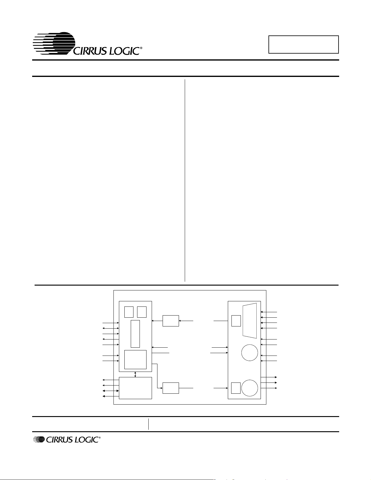
ANALOG INPUT MUX
AND OUTPUT MIXER
LINE
PCM_DATA
PCM_DATA
18 bit
ADC
20 bit
DAC
INPUT
MUX
INPUT
MIXER
Σ
OUTPUT
MIXER
Σ
CD
AUX
VIDEO
MIC1
MIC2
PHONE
PC_BEEP
LINE_OUT
HP_OUT
MONO_OUT
JULY '05
DS549PP2
1
Page 2

TABLE OF CONTENTS
1. CHARACTERISTICS AND SPECIFICATIONS ........................................................................ 7
ANALOG CHARACTERISTICS................................................................................................7
ABSOLUTE MAXIMUM RATINGS ...........................................................................................8
RECOMMENDED OPERATING CONDITIONS .......................................................................8
AC ’97 SERIAL PORT TIMING............................................................................................... 10
2. GENERAL DESCRIPTION .....................................................................................................13
2.1 AC-Link ............................... ... .... ...................................... .... ... ... ... ... .... ............................13
2.2 Control Registers .......................... ... ....................................... ... ... ... .... ... ... ......................14
2.3 Sample Rate Converters ........................ .... ... ... ... .... ... ... ....................................... ... ... ... ... 14
2.4 Mixers ........................................................ ... ....................................... ... ... ... ...................14
2.5 Input Mux ................................... ... ... ....................................... ... ... ... .... ... ... ......................14
2.6 Volume Control ............................. ... ... ....................................... ... ... .... ... ... ... ...................14
3. AC-LINK FRAME DEFINITION ..............................................................................................16
3.1 AC-Link Serial Data Output Frame .................................................................................. 17
3.1.1 Serial Data Output Slot Tags (Slot 0)............................................................................. 17
3.1.2 Command Address Port (Slot 1)....................................................................................17
3.1.3 Command Data Port (Slot 2).......................................................................................... 18
3.1.4 PCM Playback Data (Slots 3-4,6-11)............................................................................. 18
3.1.5 GPIO Pin Control (Slot12)........................... ... ... .... ... ... ....................................... ... ... ... ... 18
3.2 AC-Link Serial Data Input Frame ..................... ............................................................. ... 19
3.2.1 Serial Data Input Slot Tag Bits (Slot 0) ........................................................................ 19
3.2.2 Status Address Port (Slot 1) ..........................................................................................19
3.2.3 Status Data Port (Slot 2)................................................................................................20
3.2.4 PCM Capture Data (Slot 3-4,6-8,11)..............................................................................20
3.2.5 GPIO Pin Status (Slot 12) .......... ... ... ... .... ... ... ... .... ... ....................................... ... ... ... ... ... 20
3.3 AC-Link Protocol Violation - Loss of SYNC ............................................................ ... ... ... 21
4. REGISTER INTERFACE ..................................................................................................... 22
4.1 Reset Register (Index 00h) ........... ... ... ... .... ... ... ... .... ... ... .......................................... ... ......23
4.2 Analog Mixer Output Volume Registers (Index 02h - 04h) ..............................................23
4.3 Mono Volume Register (Index 06h)............................... ... .... ......................................... ... 24
CS4202
Contacting Cirrus Logic Support
For a complete listing of Direct Sales, Distributor, and Sales Representative contacts, visit the Cirrus Logic web site at:
http://www.cirrus.com/corporate/contacts/sales.cfm
IMPORTANT NOTICE
"Preliminary" product information describes products that are in production, but for which full characterization data is not yet available. Cirrus Logic, Inc. and its
subsidiaries ("Cirr us") belie ve that the i nformation contained i n this document i s accurate a nd reliabl e. However, the information is subject to change without
notice and is provided "AS IS" without warranty of any kind (express or implied). Customers are advised to obtain the latest version of relevant information to
verify, before placing orders, that information being relied on is current and complete. All products are sold subject to the terms and conditions of sale supplied
at the time of order acknowle dgme nt, inclu ding those p ertain ing to w arranty, ind emni ficatio n, and lim itatio n of liab ility. No responsibility is assumed by Cirrus for
the use of this information, including use of this information as the basis for manufacture or sale of any items, or for infringement of patents or other rights of
third parties. Thi s document is the prop erty of Cirrus and by furnish ing thi s inform ation, Cir rus gran ts no lic ense, expr ess or implied under any patents, mask
work rights, copyrights, trademarks, trade secrets or other intellectual property rights. Cirrus owns the copyrights associated with the information contained herein and gives consent for copies to be m ad e of th e information only for use within your orga ni zatio n with respect to Cirrus integrated circuits or other pr oducts of
Cirrus. This consent does not extend to other copying such as copying for general distribution, advertising or promotional purposes, or for creating any work for
resale.
CERTAIN APPLICATIONS USING SEMICONDUCTOR PRODUCTS MAY INVOLVE POTENTIAL RISKS OF DEATH, PERSONAL INJURY, OR SEVERE
PROPERTY OR ENVIRONMENTAL DAMAGE (“CRITICAL APPLICATIONS”). CIRRUS PRODUCTS ARE NOT DESIGNED, AUTHORIZED OR WARRANTED
FOR USE IN AIRCRAFT SYSTEMS, MILITARY APPLICATIONS, PRODUCTS SURGICALLY IMPLANTED INTO THE BODY, AUTOMOTIVE SAFETY OR SECURITY DEVICES, LIFE SUPPORT PRODUCTS OR OTHER CRITICAL APPLICATIONS. INCLUSION OF CIRRUS PRODUCTS IN SUCH APPLICATIONS
IS UNDERSTOOD TO BE FULLY AT THE CUSTOMER’S RISK AND CIRRUS DISCLAIMS AND MAKES NO WARRANTY, EXPRESS, STATUTORY OR IMPLIED, INCLUDING THE IMPLIED WARRANTIES OF MERCHANTABILITY AND FITNESS FOR PARTICULAR PURPOSE, WITH REGARD TO ANY CIRRUS
PRODUCT THAT IS USED IN SUCH A MANNER. IF THE CU ST OMER OR CUSTOMER’S CUSTOMER USES OR PERMITS THE USE OF CIRRU S P RODUCTS IN CRITICAL APPLICATIONS, CUSTOMER AGREES, BY SUCH USE, TO FULLY INDEMNIFY CIRRUS, ITS OFFICERS, DIRECTORS, EMPLOYEES,
DISTRIBUTORS AND OTHER AGENTS FR OM ANY AND ALL LI ABILI TY, INCL UDING AT TORNEYS ’ FEES AND COSTS, THA T MAY RE SULT F ROM OR
ARISE IN CONNECTION WITH THESE USES.
Cirrus Logic, Cirrus, and the Cirrus Logic logo designs are trademarks of Cirrus Logic, Inc. All other brand and product names in this document may be trademarks or service marks of their respective owners.
2 DS549PP2
Page 3

CS4202
4.4 PC_BEEP Volume Register (Index 0Ah).......................................................................... 24
4.5 Phone Volume Register (Index 0Ch)....................... ... ... ... .... ... ... ... ... .... ... ... ... .... ... ............ 24
4.6 Microphone Volume Register (Index 0Eh)........................................................................ 25
4.7 Analog Mixer Input Gain Registers (Index 10h - 18h) ...................................................... 26
4.8 Input Mux Select Register (Index 1Ah)............................................................................. 27
4.9 Record Gain Register (Index 1Ch) ...... ... .......................................................................... 28
4.10 General Purpose Register (Index 20h) ......... ... .... ... ... ... ....................................... ... ... ... 29
4.11 Powerdown Control/Status Register (Index 26h) ........................................................... 30
4.12 Extended Audio ID Register (Index 28h)........................................................................ 31
4.13 Extended Audio Status/Control Register (Index 2Ah) .................................................... 32
4.14 Audio Sample Rate Control Registers (Index 2Ch - 32h)......... ... ................................... 33
4.15 S/PDIF Control Register (Index 3Ah) ............................................................................. 34
4.16 Extended Modem ID Register (Index 3Ch) .................................................................... 35
4.17 Extended Modem Status/Control Register (Index 3Eh) ................................................. 35
4.18 GPIO Pin Configuration Register (Index 4Ch)................................................................ 35
4.19 GPIO Pin Polarity/Type Configuration Register (Index 4Eh).......................................... 36
4.20 GPIO Pin Sticky Register (Index 50h) ............................................................................ 36
4.21 GPIO Pin Wakeup Mask Register (Index 52h)............................................................... 37
4.22 GPIO Pin Status Register (Index 54h)............................................................................ 37
4.23 AC Mode Control Register (Index 5Eh).......................................................................... 37
4.24 Misc. Crystal Control Register (Index 60h)..................................................................... 39
4.25 Serial Port Control Register (Index 6Ah) ........................................................................ 40
4.26 BIOS-Driver Interface Control Registers (Index 70h - 72h) ............................................ 41
4.27 BIOS-Driver Interface Status Register (Index 7Ah)........................................................ 41
4.28 Vendor ID1 Register (Index 7Ch) ................................................................................... 42
4.29 Vendor ID2 Register (Index 7Eh) ................................................................................... 42
5. SERIAL DATA PORTS ........................................................................................................... 43
5.1 Overview ............. ....................................... ... ... ... .... ... ... ....................................... ... ......... 43
5.2 Multi-Channel Expansion ........... ... ... ... ... .... ... ... ... .... ... ... ... .......................................... ... ... 43
5.3 Serial Data Formats ............... .... ...................................... .... ... ... ... ... .... ... ... ...................... 44
6. SONY/PHILIPS DIGITAL INTERFACE (S/PDIF) ................................................................... 45
7. EXCLUSIVE FUNCTIONS ...................................................................................................... 45
8. POWER MANAGEMENT ....................................................................................................... 46
8.1 AC ’97 Reset Modes ........................................................................................................ 46
8.1.1 Cold Reset .................... ...................................... .... ... ... ... ................................... 46
8.1.2 Warm Reset ........ ... ... .... ... ... ....................................... ... ... ... .... ... ... ...................... 46
8.1.3 New Warm Reset ................................ ... .... ... ... ... .... ... ... ...................................... 46
8.1.4 Register Reset .................... ... ... .... ...................................................................... 46
8.2 Powerdown Controls .................................... ... ... .... ... ... ... .... ... ... ... ................................... 47
9. CLOCKING ............................................................................................................................. 49
9.1 PLL Operation (External Clock) ....................................................................................... 49
9.2 24.576 MHz Crystal Operation ........................................................................................ 49
9.3 Secondary Codec Operation ........................................................................................... 49
10. ANALOG HARDWARE DESCRIPTION ............................................................................... 51
10.1 Analog Inputs ................................................................................................................. 51
10.1.1 Line Inputs ........................................................................................................ 51
10.1.2 CD Input ............................................................................................................ 51
10.1.3 Microphone Inputs ............................................................................................ 51
10.1.4 PC Beep Input ................................................................................................... 52
10.1.5 Phone Input ....................................................................................................... 52
10.2 Analog Outputs .............................................................................................................. 52
10.2.1 Stereo Outputs .................................................................................................. 52
10.2.2 Mono Output ..................................................................................................... 53
10.3 Miscellaneous Analog Signals ....................................................................................... 53
DS549PP2 3
Page 4

10.4 Power Supplies ..............................................................................................................53
10.5 Reference Design ..........................................................................................................53
11. GROUNDING AND LAYOUT .............................................................................................. 54
12. PIN DESCRIPTIONS ........................................................................................................ 56
13. PARAMETER AND TERM DEFINITIONS ............................................................................ 62
14. REFERENCE DESIGN ................................................................................................... 64
15. REFERENCES ................................ ... ... ... ....................................... ... ... .... ... ... ... .... ... ... ......... 65
16. PACKAGE DIMENSIONS ..................................................................................................... 66
LIST OF FIGURES
Figure 1. Power Up Timing............................................................................................................11
Figure 2. Codec Ready from Start-up or Fault Condition..............................................................11
Figure 3. Clocks ............................................................................................................................11
Figure 4. Data Setup and Hold......................................................................................................12
Figure 5. PR4 Powerdown and Warm Reset ................................................................................12
Figure 6. Test Mode......................................................................................................................12
Figure 7. AC-link Connections.......................................................................................................13
Figure 8. CS4202 Mixer Diagram..................................................................................................15
Figure 9. AC-link Input and Output Framing.................................................................................. 16
Figure 10. Serial Data Port: Six Channel Circuit ...........................................................................43
Figure 11. Serial Data Format 0 (I2S)...........................................................................................44
Figure 12. Serial Data Format 1 (Left Justified) ............................................................................44
Figure 13. Serial Data Format 2 (Right Justified, 20-bit data).......................................................44
Figure 14. Serial Data Format 3 (Right Justified, 16-bit data).......................................................44
Figure 15. S/PDIF Output..............................................................................................................45
Figure 16. PLL External Loop Filter............................................................................................... 49
Figure 17. External Crystal............................................................................................................50
Figure 18. Line Input (Replicate for Video and AUX) ....................................................................51
Figure 19. Differential 1 VRMS CD Input ......................................................................................51
Figure 20. Microphone Input .........................................................................................................52
Figure 21. PC_BEEP Input............................................................................................................ 52
Figure 22. Modem Connection......................................................................................................52
Figure 23. Line Out and Headphone Out Setup............................................................................53
Figure 24. Line Out/Headphone Out Setup................................................................................... 53
Figure 25. +5V Analog Voltage Regulator.....................................................................................54
Figure 26. Conceptual Layout for the CS4202 when in XTAL or OSC Clocking Modes...............55
Figure 27. Pin Locations for the CS4202 ......................................................................................56
Figure 28. CS4202 Reference Design ..........................................................................................64
CS4202
4 DS549PP2
Page 5

LIST OF TABLES
Table 1. Register Overview for the CS4202.....................................................................22
Table 2. Analog Mixer Output Attenuation........................................................................23
Table 3. Microphone Input Gain Values ...........................................................................25
Table 4. Analog Mixer Input Gain Values.........................................................................26
Table 5. Analog Mixer Input Gain Register Index.............................................................26
Table 6. Input Mux Selection.................................. ... .... ... ... ... .... ... ... ................................27
Table 7. Record Gain Values ...........................................................................................28
Table 8. Slot Mapping for the CS4202 .............................................................................31
Table 9. Slot Assignment Defaults ...................................................................................31
Table 10. Directly Supported SRC Sample Rates for the CS4202...................................33
Table 11. GPIO Input/Output Configurations....................................................................36
Table 12. Serial Data Format Selection............................................................................40
Table 13. Device ID with Corresponding Part Number.....................................................42
Table 14. Serial Data Formats and Compatible DACs for the CS4202............ ... .... ... ... ...44
Table 15. Powerdown PR Bit Functions........................................ ... ... .............................47
Table 16. Powerdown PR Function Matrix for the CS4202..............................................48
Table 17. Power Consumption by Powerdown Mode for the CS4202 .............................48
Table 18. Clocking Configurations for the CS4202 ..........................................................50
CS4202
DS549PP2 5
Page 6
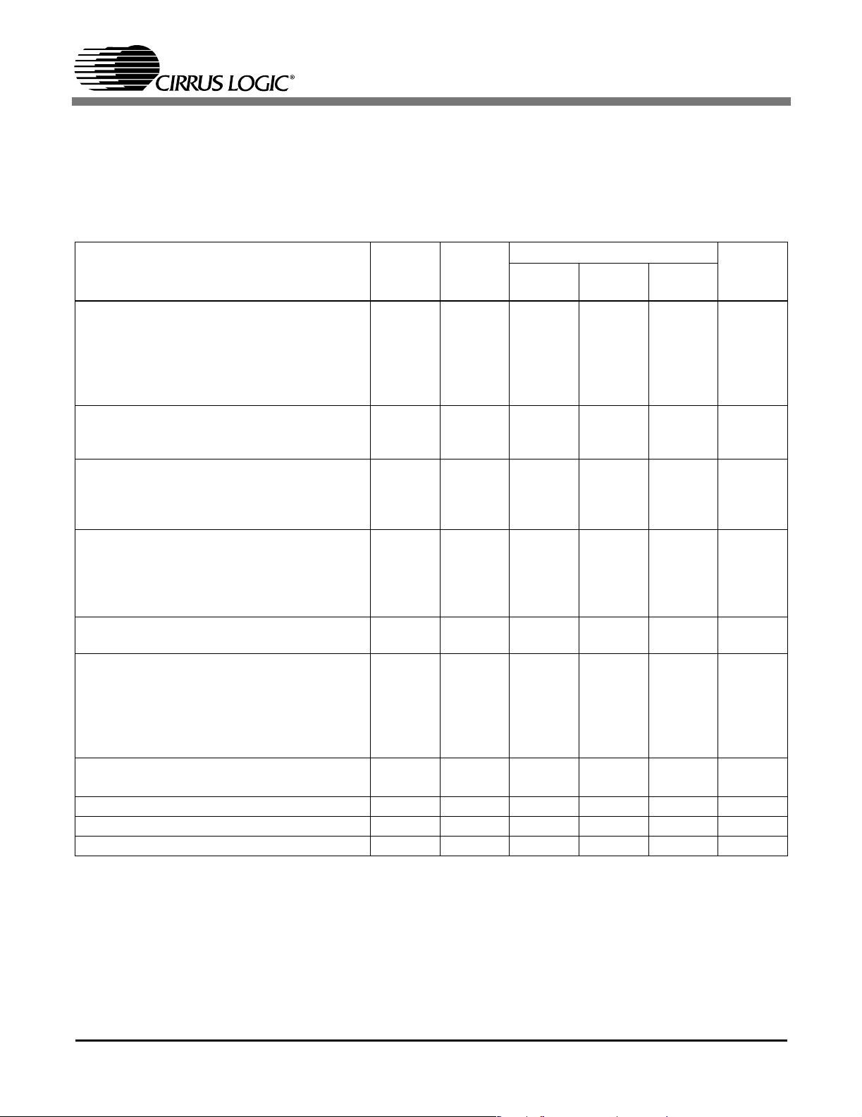
1. CHARACTERISTICS AND SPECIFICATIONS
CS4202
ANALOG CHARACTERISTICS (Standard test conditions unless otherwise noted: T
AVdd = 5.0 V ±5%, DVdd = 3.3 V ±5%; 1 kHz Input Sine wave; Sample Frequency, Fs = 48 kHz; Z
1000 pF load for Mono and Line Outputs; C
= 18 pF load (Note 1); Measurement bandwidth is 20 Hz - 20 kHz,
DL
ambient
=100 kΩ/
AL
= 25° C,
18-bit linear coding for ADC functions, 20-bit linear coding for DAC functions; Mixer registers set for unity gain.
Parameter
(Note 2)
Symbol Path
(Note 3)
CS4202-JQZ
Min Typ Max
Unit
Full Scale Input Voltage
Line Inputs
Mic Inputs (10dB = 0, 20dB = 0)
Mic Inputs (10dB = 1, 20dB = 0)
Mic Inputs (10dB = 0, 20dB = 1)
Mic Inputs (10dB = 1, 20dB = 1)
A-D
A-D
A-D
A-D
A-D
0.91
0.91
0.283
0.091
0.0283
1.00
1.00
0.315
0.10
0.0315
-
-
-
-
-
V
V
V
V
V
RMS
RMS
RMS
RMS
RMS
Full Scale Output Voltage
Line and Mono Outputs
Headphone Output
Frequency Response (Note 4)
Analog Ac = ± 0.25 dB
DAC Ac = ± 0.25 dB
ADC Ac = ± 0.25 dB
Dynamic Range
Stereo Analog Input s to LINE_OUT
Mono Analog Input to LINE_OUT
DAC Dynamic Range
ADC Dynamic Range
DAC SNR
(-20 dB FS input w/ CCIR-RMS filter on output)
Total Harmonic Distortion + Noise
FR
DR
SNR
THD+N
D-A
D-A
A-A
D-A
A-D
A-A
A-A
D-A
A-D
0.91
-
20
20
20
90
85
85
85
1.0
1.4
-
-
-
95
90
90
90
1.13
-
20,000
20,000
20,000
-
-
-
-
V
RMS
V
RMS
Hz
Hz
Hz
dB FS A
dB FS A
dB FS A
dB FS A
D-A - 70 - dB
(-3 dB FS input signal):
Line Output
Headphone Output
DAC
ADC (all inputs)
A-A
A-A
D-A
A-D
-
-
-
-
-90
-75
-87
-84
-80
-70
-80
-80
dB FS
dB FS
dB FS
dB FS
Power Supply Rejection Ratio
(1 kHz, 0.5 V
w/ 5V DC offs e t ) (Note 4) 40 60 - dB
RMS
Interchannel Isolation 70 87 - dB
Spurious Tone (Note 4) - -100 - dB FS
Input Impedance (Note 4) 10 - - kΩ
Notes: 1. Z
refers to the analog output pin loading and CDL refers to the digital output pin loading.
AL
2. Parameter definitions are given in Section 13, Parameter and Term Definitions.
3. Path refers to the signal path used to generate this data. These paths are defined in Section 13,
Parameter and Term Definitions.
4. This specification is guaranteed by silicon characterization; it is not production tested.
6 DS549PP2
Page 7
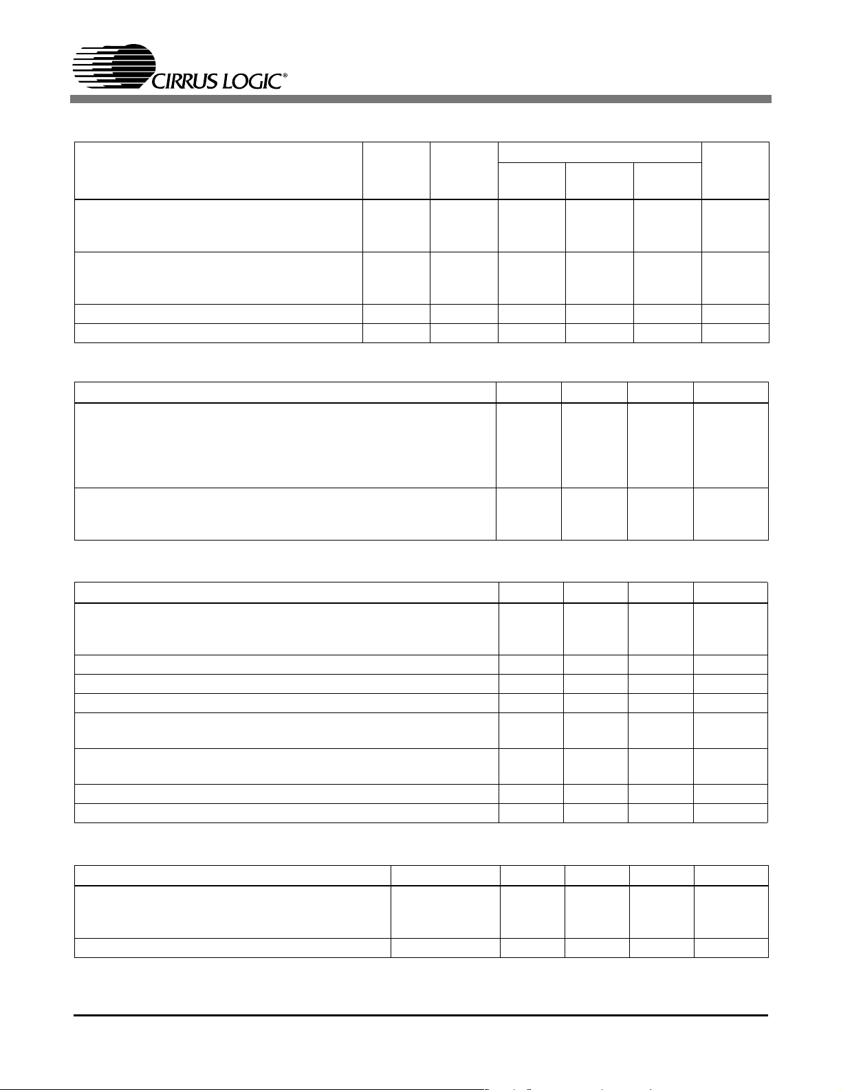
ANALOG CHARACTERISTICS (Continued)
CS4202
Parameter
(Note 2)
External Load Impedance
Line Output, Mono Output
Headphone Output
Output Impedance
Line Output, Mono Output
Headphone Output (Note 4)
Input Capacitance (Note 4) - 5 - pF
Vrefout 2.3 2.4 2.5 V
Symbol Path
(Note 3)
CS4202-JQZ
Min Typ Max
10
32
-
-
-
-
730
0.8
-
-
-
-
Unit
kΩ
MIXER CHARACTERISTICS
Parameter Min Typ Max Unit
Mixer Gain Range Span
PC Beep
Line In, Aux, CD, Video, Mic1, Mic2, Phone
Mono Out, Line Out, Headphone Out
ADC Gain
Step Size
All volume controls except PC Beep
PC Beep
-
-
-
-
-
-
45.0
46.5
46.5
22.5
1.5
3.0
-
-
-
-
-
-
dB
dB
dB
dB
dB
dB
Ω
Ω
Ω
ABSOLUTE MAXIMUM RATINGS (AVss1 = AVss2 = DVss1 = DVss2 = 0 V)
Parameter Min Typ Max Unit
Power Supplies +3.3 V Digital
+5 V Digital
Analog
Total Power Dissipation (Supplies, Inputs, Outputs) - - 1.25 W
Input Current per Pin (Except Supply Pins) -10 - 10 mA
Output Current per Pin (Except Supply Pins) -15 - 15 mA
Analog Input voltage -0.3 - AVdd+
Digital Input voltage -0.3 - DVdd +
Ambient Temperature (Power Applied) 0 - 70 °C
Storage Temperature -65 - 150 °C
-0.3
-0.3
-0.3
-
-
-
5.5
5.5
5.5
0.3
0.3
RECOMMENDED OPERATING CONDITIONS (AVss1 = AVss2 = DVss1 = DVss2 = 0 V)
Parameter Symbol Min Typ Max Unit
Power Supplies +3.3 V Digital
+5 V Digital
Analog
Operating Ambient Temperature 0 - 70 °C
DVdd1, DVdd2
DVdd1, DVdd2
AVdd1, AVdd2
3.135
4.75
4.75
3.3
5
5
3.465
5.25
5.25
V
V
V
V
V
V
V
V
DS549PP2 7
Page 8
CS4202
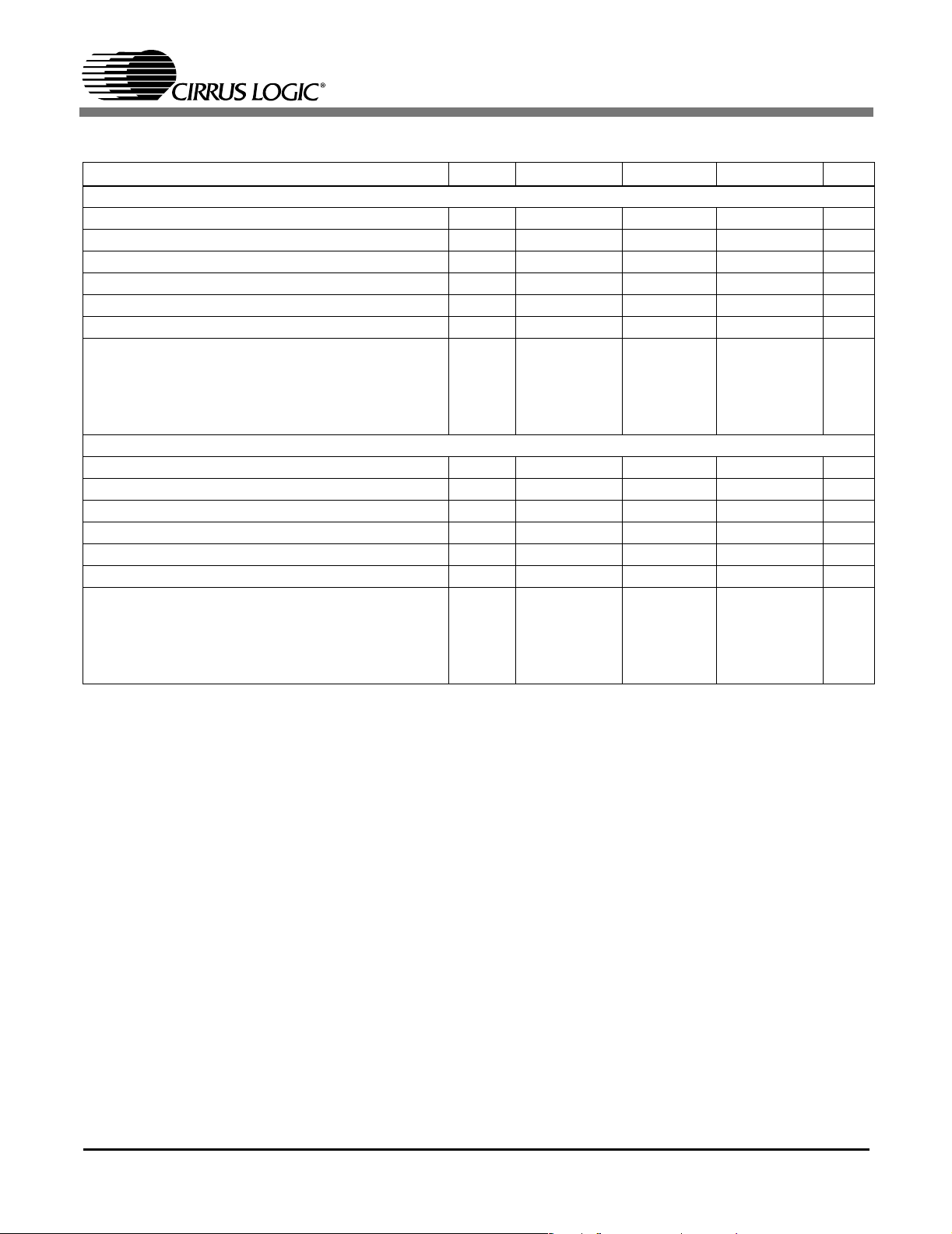
DIGITAL CHARACTERISTICS (AVss1 = AVss2 = DVss1 = DVss2 = 0 V)
Parameter Symbol Min Typ Max Unit
DVdd = 3.3V
Low level input voltage V
High level input voltage V
High level output voltage V
Low level output voltage V
il
ih
oh
ol
Input Leakage Current (AC-link inputs) -10 - 10 µA
Output Leakage Current (Tri-stated AC-link outputs) -10 - 10 µA
Output buffer drive current
BIT_CLK, SDATA_IN
SPDIF_OUT
EAPD/SCLK, GPIO0/LRCLK, GPIO1/SDOUT,
GPIO2, GPIO3, GPIO4/SDO2 (Note 4)
DVdd = 5.0 V
Low level input voltage V
High level input voltage V
High level output voltage V
Low level output voltage V
il
ih
oh
ol
Input Leakage Current (AC-link inputs) -10 - 10 µA
Output Leakage Current (Tri-stated AC-link outputs) -10 - 10 µA
Output buffer drive current
BIT_CLK, SDATA_IN
SPDIF_OUT
EAPD/SCLK, GPIO0/LRCLK, GPIO1/SDOUT,
GPIO2, GPIO3, GPIO4/SDO2 (Note 4)
- - 0.80 V
2.15 - - V
3.00 3.25 - V
-0.030.35V
-
-
-
72
24
4
-
-
-
mA
mA
mA
- - 0.80 V
3.25 - - V
4.50 4.95 - V
- 0.03 0.35 V
-
-
-
72
24
4
-
-
-
mA
mA
mA
8 DS549PP2
Page 9
CS4202
AC ’97 SERIAL PORT TIMING Standard test conditions unless otherwise noted: T
AVdd = 5.0 V, DVdd = 3.3 V; C
= 55 pF load.
L
ambient
= 25° C,
Parameter Symbol Min Typ Max Unit
RESET Timing
RESET# active low pulse width T
RESET# inactive to BIT_CLK start-up delay (XTL mode)
(OSC mode)
(PLL mode)
1st SYNC active to CODEC READY ‘set’ T
Vdd stable to RESET# inactive T
rst_low
T
rst2clk
sync2crd
vdd2rst#
1.0 - - µs
-
-
-
4.0
4.0
2.5
-
-
-
-62.5-µs
100 - - µs
Clocks
BIT_CLK frequency F
BIT_CLK period T
clk_period
clk
- 12.288 - MHz
- 81.4 - ns
BIT_CLK output jitter (depends on XTL_IN source) - - 750 ps
BIT_CLK high pulse width T
BIT_CLK low pulse width T
SYNC frequency F
SYNC period T
SYNC high pulse width T
SYNC low pulse width T
sync_period
sync_high
sync_low
clk_high
clk_low
sync
36 40.7 45 ns
36 40.7 45 ns
- 48 - kHz
-20.8-µs
-1.3-µs
-19.5-µs
Data Setup and Hold
Output propagation delay from rising edge of BIT_CLK T
Input setup time from falling edge of BIT_CLK T
Input hold time from falling edge of BIT_CLK T
Input signal rise time T
Input signal fall time T
Output signal rise time (Note 4) T
Output signal fall time (Note 4) T
co
isetup
ihold
irise
ifall
orise
ofall
81012ns
10 - - ns
0--ns
2-6ns
2-6ns
246ns
246ns
Misc. Timing Parameters
End of Slot 2 to BIT_CLK, SDATA_IN low (PR4) T
SYNC pulse width (PR4) Warm Reset T
SYNC inactive (PR4) to BIT_CLK start-up delay T
Setup to trailing edge of RESET# (ATE test mode) (Note 4) T
s2_pdown
sync_pr4
sync2clk
setup2rst
Rising edge of RESET# to Hi-Z delay (Note 4) T
off
- 0.285 1.0 µs
1.0 - - µs
162.8 285 - ns
15 - - ns
- - 25 ns
µs
µs
ms
DS549PP2 9
Page 10
BIT_CLK
RESET#
Vdd
BIT_CLK
T
rst_low
T
vdd2rst#
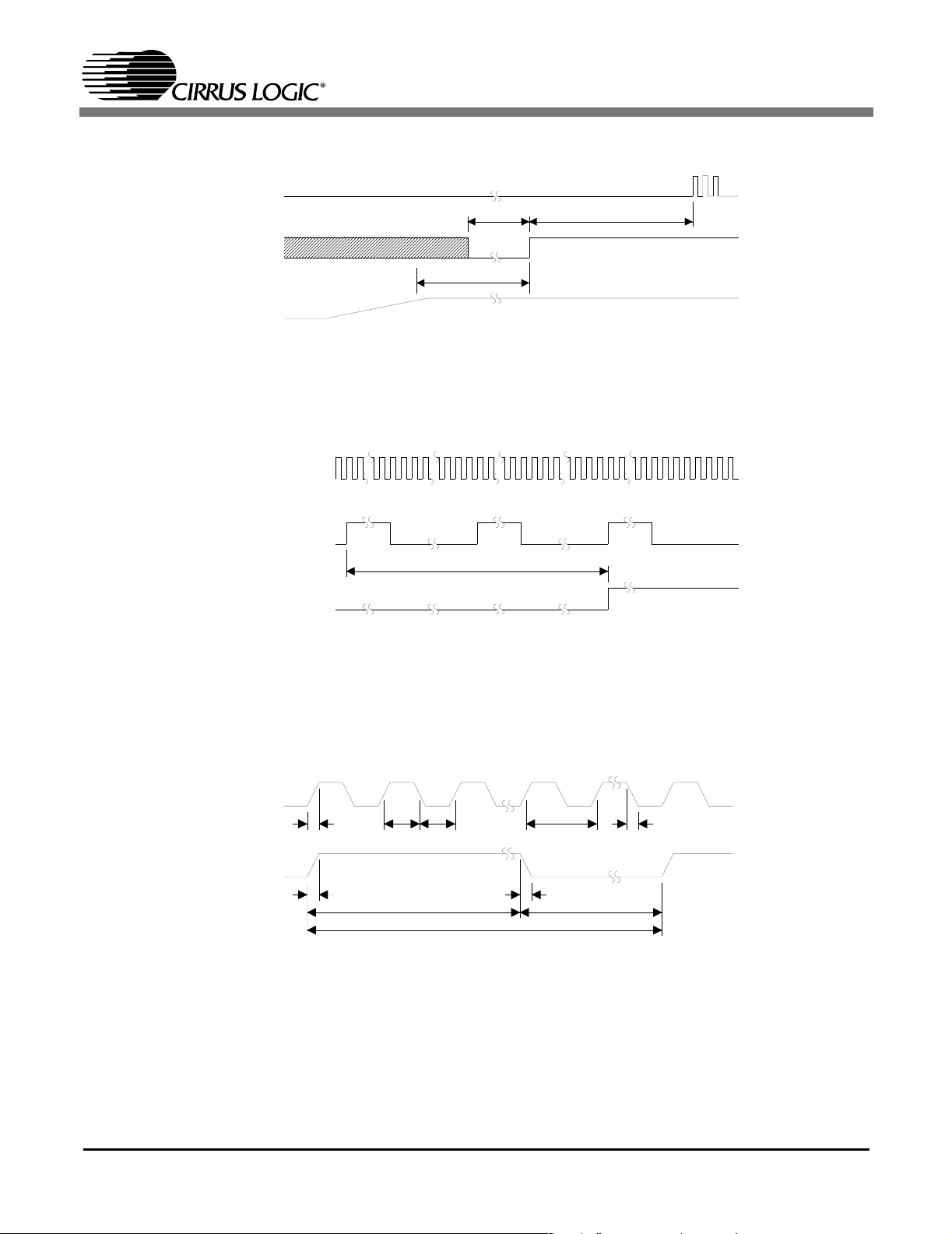
Figure 1. Power Up Timing
T
rst2clk
CS4202
SYNC
CODEC_READY
Figure 2. Codec Ready from Start-up or Fault Condition
BIT_CLK
T
orise
SYNC
T
irise
T
clk_highTclk_low
T
sync_high
T
T
sync2crd
T
ifall
sync_period
T
clk_period
T
sync_low
T
ifall
Figure 3. Clocks
10 DS549PP2
Page 11
BIT_CLK
BIT_CLK
SDATA_IN
SDATA_OUT,
SYNC
Slot 1 Slot 2
T
co
T
isetup
Figure 4. Data Setup and Hold
T
CS4202
ihold
SDATA_OUT
SDATA_IN
SYNC
Write to 0x20 Data PR4 Don't Care
T
s2_pdown
Figure 5. PR4 Powerdown and Warm Reset
RESET#
T
setup2rst
SDATA_OUT,
SYNC
T
off
T
sync_pr4
T
sync2clk
SDATA_IN,
BIT_CLK
Hi-Z
Figure 6. Test Mode
DS549PP2 11
Page 12

CS4202
2. GENERAL DESCRIPTION
The CS4202 is a mixed-signal serial audio codec
with integrated headphone power amplifier compliant with the Intel® Audio Codec ’97 Specifica-
tion, revision 2.2 [6] (referred to as AC ’97). It is
designed to be paired with a digital controller, typically located on the PCI bus or integrated within
the system core logic chip set. The controller is responsible for all communications between the
CS4202 and the remainder of the system. The
CS4202 contains two distinct functional sections:
digital and analog. The digital section includes the
AC-link interface, S/PDIF interface, serial data
port, GPIO, power management support, and Sample Rate Converters (SRCs). The analog section includes the analog input multiplexer (mux), stereo
input mixer, stereo output mixer, mono output mixer, headphone amplifier, stereo Analog-to-Digital
Converters (ADCs), stereo Digital-to-Analog Converters (DACs), and their associated volume controls.
2.1 AC-Link
All communication with the CS4202 is established
with a 5-wire digital interface to the controller
called the AC-link. This interface is shown in
Figure 7. All clocking for the serial communication
is synchronous to the BIT_CLK signal. BIT_CLK
is generated by the primary audio codec and is used
to clock the controller and any secondary audio codecs. Both input and output AC-link audio frames
are organized as a sequence of 256 serial bits forming 13 groups referred to as ‘slots’. During each audio frame, data is passed bi-directionally between
the CS4202 and the controller. The input frame is
driven from the CS4202 on the SDATA_IN line.
The output frame is driven from the controller on
the SDATA_OUT line. The controller is also responsible for issuing reset commands via the RESET# signal. Following a Cold Reset, the CS4202
is responsible for notifying the controller that it is
ready for operation after synchronizing its internal
functions. The CS4202 AC-link signals must use
the same digital supply voltage as the controller, either +5 V or +3.3 V. See Section 3, AC-Link Frame
Definition, for detailed AC-link information.
Digital AC'97
Controller
Figure 7. AC-link Connections
12 DS549PP2
SYNC
BIT_CLK
SDATA_OUT
SDATA_IN
RESET#
AC'97
CODEC
Page 13

CS4202
2.2 Control Registers
The CS4202 contains a set of AC ’97 compliant
control registers, and a set of Cirrus Logic defined
control registers. These registers control the basic
functions and features of the CS4202. Read accesses of the control registers by the AC ’97 controller
are accomplished with the requested register index
in Slot 1 of a SDATA_OUT frame. The following
SDATA_IN frame will contain the read data in Slot
2. Write operations are similar, with the register index in Slot 1 and the write data in Slot 2 of a
SDATA_OUT frame. The function of each input
and output frame is detailed in Section 3, AC-Link
Frame Definition. Individual register descriptions
are found in Section 4, Register Interface.
2.3 Sample Rate Converters
The sample rate converters (SRC) provide high accuracy digital filters supporting sample frequencies
other than 48 kHz to be captured from the CS4202
or played from the controller. AC ’97 requires support for two audio rates (44.1 and 48 kHz). In addition, the Intel® I/O Controller Hub (ICHx)
specification [9] requires support for five more audio rates (8, 11.025, 16, 22.05, and 32 kHz). The
CS4202 supports all these rates, as shown in
Table 10 on page 32.
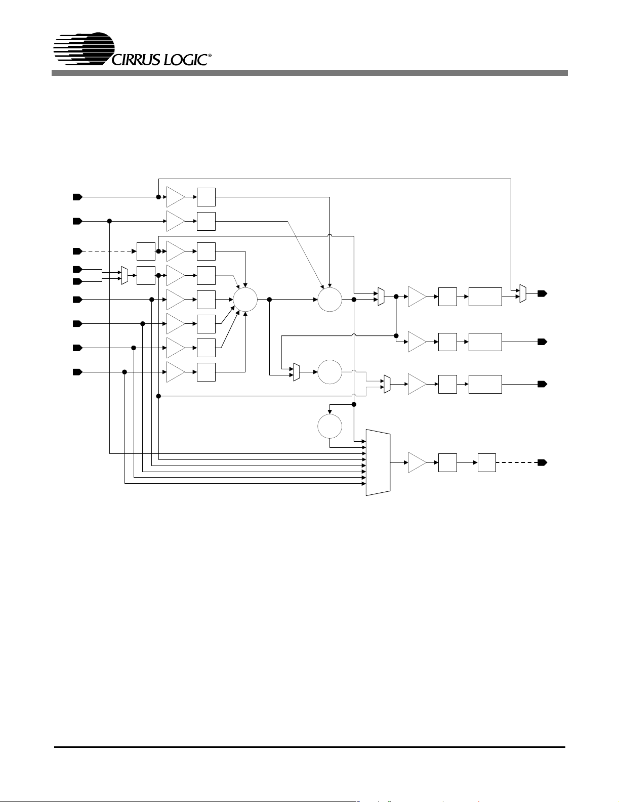
2.4 Mixers
The CS4202 input and output mixers are illustrated
in Figure 8. The stereo input mixer sums together
the analog inputs to the CS4202 according to the
settings in the volume control registers. The stereo
output mixer sums the output of the stereo input
mixer with the PC_BEEP and PHONE signals. The
stereo output mix is then sent to the LINE_OUT
and HP_OUT pins of the CS4202. The mono output mixer generates a monophonic sum of the left
and right audio channels from the stereo input mixer. The mono output mix is then sent to the
MONO_OUT pin on the CS4202.
2.5 Input Mux
The input multiplexer controls which analog input
is sent to the ADCs. The output of the input mux is
converted to stereo 18-bit digital PCM data and
transmitted to the controller by means of the
AC-link SDATA_IN signal.
2.6 Volume Control
The CS4202 volume registers control analog input
levels to the input mixer and analog output levels,
including the master volume level. The PC_BEEP
volume control uses 3 dB steps with a range of 0 dB
to -45 dB attenuation. All other analog volume controls use 1.5 dB steps. The analog inputs have a
mixing range of +12 dB signal gain to -34.5 dB signal attenuation. The analog output volume controls
have a range of 0 dB to -46.5 dB attenuation for
LINE_OUT, HP_OUT and MONO_OUT.
DS549PP2 13
Page 14
CS4202
PC_BEEP
PHONE
PCM_OUT
MIC1
MIC2
LINE
CD
VIDEO
AUX
MIC
SELECT
MAIN D/A
CONVERTERS
DAC
BOOST
MUTE
MUTE
MUTE
MUTE
MUTE
MUTE
MUTE
MUTE
PC BEEP BYPASS
ANALOG STEREO
Σ
INPUT MIXER
MONO MIX
SELECT
STEREO TO
MONO MIXER
Σ
ANALOG STEREO
OUTPUT MIXER
STEREO TO
MONO MIXER
Σ
1/2
Σ
1/2
DAC DIRECT
MODE
MONO OUT
SELECT
ADC
INPUT
MUX
MASTER
VOLUME
VOL VOL
HEADPHONE
VOLUME
MONO
VOLUME
VOL
MAIN ADC
GAIN
VOL
MUTE
MUTE
MUTE
OUTPUT
BUFFER
HEADPHONE
AMPLIFIER
OUTPUT
BUFFER
MAIN A/D
CONVERTERS
ADCMUTE
LINE OUT
HEADPHONE OUT
MONO OUT
PCM_IN
VOL
VOL
VOL
VOL VOL
VOL VOL VOL
Figure 8. CS4202 Mixer Diagram
14 DS549PP2
Page 15
CS4202
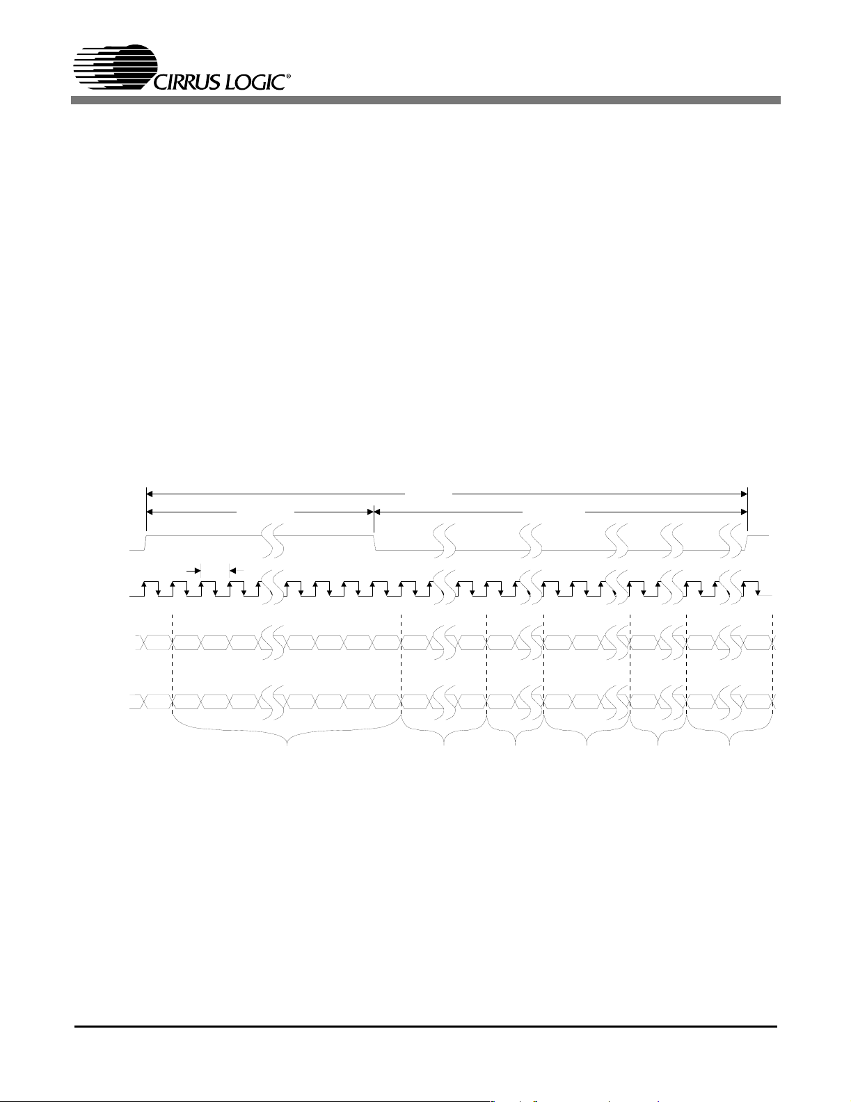
3. AC-LINK FRAME DEFINITION
The AC-link is a bi-directional serial port with data
organized into frames consisting of one 16-bit and
twelve 20-bit time-division multiplexed slots.
Slot 0 is a special reserved time slot containing
16-bits which are used for AC-link protocol infrastructure. Slots 1 through 12 contain audio or control/status data. Both the serial data output and
input frames are defined from the controller perspective, not from the CS4202 perspective.
The controller synchronizes the beginning of a
frame with the assertion of the SYNC signal.
Figure 9 shows the position of each bit location
Tag Phase Data Phase
within the frame. The first bit position in a new serial data frame is F0 and the last bit position in the
serial data frame is F255. When SYNC goes active
(high) and is sampled active by the CS4202 (on the
falling edge of BIT_CLK), both devices are synchronized to a new serial data frame. The data on
the SDATA_OUT pin at this clock edge is the final
bit of the previous frame’s serial data. On the next
rising edge of BIT_CLK, the first bit of Slot 0 is
driven by the controller on the SDATA_OUT pin.
On the next falling edge of BIT_CLK, the CS4202
latches this data in as the first bit of the frame.
20.8 µs
(48 kHz)
SYNC
BIT_CLK
Bit Frame Position:
SDATA_OUT
Bit Frame Position:
SDATA_IN
12.288 MHz
81.4 ns
F0 F1 F2 F16F15F14F13F12
F255
Valid
Frame
F0 F1 F2 F16F15F14F13F12 F35 F56 F76F255
Codec
Ready
Slot 1
Valid
Slot 1
Valid
GPIO
INT
0
Slot 2
Valid
Slot 2
Valid
Slot 12
Valid
Slot 12
Valid
Slot 0 Slot 1 Slot 2 Slot 3 Slot 4 Slots 5-12
Codec
Codec
0
ID1
R/W 0 WD15
ID0
0000
Figure 9. AC-link Input and Output Framing
F36 F57
F35
F36
0
F56
D19 D18
F57
D19 D18 D19RD15
F76
D19
D19
D19
F96
F96
F255
F255
GPIO
0
INT
DS549PP2 15
Page 16
CS4202
3.1 AC-Link Serial Data Output Frame
In the serial data output frame, data is passed on the SDATA_OUT pin to the CS4202 from the AC ’97
controller. Figure 9 illustrates the serial port timing.
The PCM playback data being passed to the CS4202 is shifted out MSB first in the most significant bits
of each slot. Any PCM data from the AC ’97 controller that is not 20 bits wide should be left justified in
its corresponding slot and dithered or zero-padded in the unused bit positions.
Bits that are reserved should always be ‘cleared’ by the AC ’97 controller.
3.1.1 Serial Data Output Slot Tags (Slot 0)
Bit 15 14 13 12 11 10 9 8 7 6 5 4 3 2 1 0
Valid
Slot 1
Frame
Valid
Valid Frame The Valid Frame bit determines if any of the following slots contain either valid playback data
Slot 2
Valid
Slot 3
Valid
Slot 4
Valid
Not
Implem
Slot 6
Valid
Slot 7
Valid
Slot 8
Valid
Slot 9
Valid
Slot 10
Valid
Slot 1 1
Valid
Slot 12
Valid
Res
Codec
ID1
Codec
ID0
for the CS4202 or data for read/write operatio ns. When ‘set’, at least one of th e other AC-link
slots contains valid data. If this bit is ‘clear’, the remainde r of the fr am e is ignor ed .
Slot 1 Valid The Slot 1 Valid bit indicates a valid register read/write address for a primary codec.
Slot 2 Valid The Slot 2 Valid bit indicates valid register write data for a primary codec.
Slot [3:4,6:11] Valid The Slot [3:4,6:11] Valid bits indicate the validity of data in their corresponding serial d ata out-
put slots. If a bit is ‘set’, the corresponding output slot co ntains valid data. If a bit is ‘cleared’,
the corresponding slot will be ignored.
Slot 12 Valid The Slot 12 Valid bit indicates if output Slot 12 contains valid GPIO control data.
Codec ID[1:0] The Codec ID[1:0] bits determine which codec is being accessed during the current AC-link
frame. Codec ID[1:0] = 00 indicates the primary codec is being accessed. Codec ID[1:0] = 01,
10, or 11 indicates one of three possible secondary codecs is being accessed. A Codec ID
value of 01, 10, or 11 also indicates a valid read/write add ress and/or valid register write data
for a secondary codec.
3.1.2 Command Address Port (Slot 1)
Bit 19 18 17 16 15 14 13 12 11 10 9 8 7 6 5 4 3 2 1 0
R/W
R/W Read/Write. When this bit is ‘set’, a read of the AC ’97 register specified by the register index
RI6 RI5 RI4 RI3 RI2 RI1 RI0 Reserved
bits will occur in the AC ’97 2.x audio codec. When the bit is ‘cleared’, a write will occur. For
any read or write access to occur, the Valid Frame bit (F0) must be ‘set’ and the Codec ID[1:0]
bits (F[14:15]) must match the Codec ID of the AC ’97 2.x audio codec being accessed. Ad-
ditionally, for a primary codec, the Slot 1 Valid bit (F1) must be ‘set’ for a read access and
both the Slot 1 Valid bit (F1) and the Slot 2 Valid bit (F2) must be ‘set’ for a write access. For
a secondary codec, both the Slot 1 Valid bit (F1) and th e Slot 2 Valid bit (F2) must be ‘cleared’
for read and write accesses. See Figure 9 for bit frame positions.
RI[6:0] Register Index. The RI[6:0] bits contain the 7-bit register index to the AC ’97 registers in the
CS4202. All registers are defined at word addressable boundaries. The RI0 b it must be ‘clear’
to access CS4202 registers.
16 DS549PP2
Page 17
CS4202
3.1.3 Command Data Port (Slot 2)
Bit 191817161514131211109876543210
WD15 WD14 WD13 WD12 WD11 WD10 WD9 WD8 WD7 WD6 WD5 WD4 WD3 WD2 WD1 WD0 Reserved
WD[15:0] Write Data. The WD[15:0] bits contain the 16-bit value to be written to the register. If an ac-
cess is a read, this slot is ignored.
NOTE: For any write to an AC ’97 register, the write is defined to be an ‘atomic’ access. This means
that when the Slot 1 Valid bit in output Slot 0 is ‘set’, the Slot 2 Valid bit in output Slot 0 should
always be ‘set’ during the same audio frame. No write access may be split across 2 frames.
3.1.4 PCM Playback Data (Slots 3-4,6-11)
Bit 19 18 17 16 15 14 13 12 11 10 9 8 7 6 5 4 3 2 1 0
PD19 PD18 PD17 PD16 PD15 PD14 PD13 PD12 PD11 PD10 PD9 PD8 PD7 PD6 PD5 PD4 PD3 PD2 PD1 PD0
PD[19:0] Playback Data. The PD[19:0] bits contain the 20-bit PCM (2’s complement) pl ayback data for
the left and right DACs, serial data ports, and/or the S/PDIF transmitter. Table 8 on page 30
lists a cross reference for each function and its respective slot. The mapping of a given slot
to the DAC, serial data port, or S/PDIF transmitter is determined by the state of the DSA[1:0]
bits in the Extended Audio ID Register (Index 28h) and the SPSA[1:0] bits in the Extended
Audio Status/Control Register (Index 2Ah).
3.1.5 GPIO Pin Control (Slot12)
Bit 19 18 17 16 15 14 13 12 11 10 9 8 7 6 5 4 3 2 1 0
Not Implemented GPIO4 GPIO3 GPIO2 GPIO1 GPIO0 Reserved
GPIO[4:0] GPIO Pin Control. The GPIO[4:0] bits control the CS4202 GPIO pins configured as outputs.
Write accesses using GPIO pin control bits configured as outputs will be reflected on the
GPIO pin output on the next AC-link frame. Write accesses using GPIO pin control bits configured as inputs will have no effect and are ignored. If the GPOC bit in the Misc. Crystal Con-
trol Register (Index 60h) is ‘set’, the bits in output Slot 12 are ignored and GPIO pins
configured as outputs are controlled through the GPIO Pin Status Register (Index 54h).
DS549PP2 17
Page 18

CS4202
3.2 AC-Link Serial Data Input Frame
In the serial data input frame, data is passed on the SDATA_IN pin from the CS4202 to the AC ’97 controller. The data format for the input frame is very similar to the output frame. Figure 9 on page 15 illustrates the serial port timing.
The PCM capture data from the CS4202 is shifted out MSB first in the most significant 18 bits of each slot.
The least significant 2 bits in each slot will be ‘cleared’. If the host requests PCM data from the AC ’97
Controller that is less than 18 bits wide, the controller should dither and round or just round (but not truncate) to the desired bit depth.
Bits that are reserved or not implemented in the CS4202 will always be returned ‘cleared’.
3.2.1 Serial Data Input Slot Tag Bits (Slot 0)
Bit 1514131211109876543210
Codec
Ready
Codec Ready Codec Ready. The Codec Ready bit indicates the readiness of the CS4202 AC-link. Immedi-
Slot 1
Valid
Slot 2
Valid
Slot 3
ately after a Cold Reset this bit will be ‘clear’. Once the CS4202 clocks and voltages are stable, this bit will be ‘set’. Until the Codec Ready bit is ‘set’, no AC-link transactions should be
attempted by the controller. The Codec Ready bit does not indicate readiness of the DACs,
ADCs, Vref, or any other analog function. Those must be checked in the Powerdown Con-
trol/Status Register (Index 26h) by the controller before any access is ma de to the mixer registers. Any accesses to the CS4202 while Codec Ready is ‘clear’ are ignored.
Valid
Slot 4
Valid
Slot 6
0
Valid
Slot 7
Valid
Slot 8
Valid
00
Slot 1 1
Valid
Slot 12
Valid
Reserved
Slot 1 Valid The Slot 1 Valid bit indicates Slot 1 contains a valid read back address.
Slot 2 Valid The Slot 2 Valid bit indicates Slot 2 contains valid register read data.
Slot [3:4,6:8,11] Valid The Slot [3:4,6:8,11] Valid bits indicate Slot [3:4,6:8,11] contains valid capture data from the
CS4202 ADCs. If a bit is ‘set’, the corresponding input slot contains valid data. If a bit is
‘cleared’, the corresponding slot will be ignored.
Slot 12 Valid The Slot 12 Valid bit indicates Slot 12 contains valid GPIO status data.
3.2.2 Status Address Port (Slot 1)
Bit 191817161514131211109876543210
Res RI6 RI5 RI4 RI3 RI2 RI1 RI0 SR3 SR4 0 SR6 SR7 SR8 SR9 SR10 SR11 0 Reserved
RI[6:0] Register Index. The RI[6:0] bits echo the AC ’97 register address when a register read has
been requested in the previous frame. The CS4202 will only echo the register index for a read
access. Write accesses will not return valid data in Slot 1.
SR[3:4,6:11] Slot Request. If SRx is ‘set’, this indicates the CS4202 SRC does not need a new sample on
the next AC-link frame for that particular slot. If SRx is ‘clear’, the SRC indicates a new sample
is needed on the following frame. If the VRA bit in the Extended Audio Stat us/Control Register
(Index 2Ah)
abled and the SR[3:4,6:11] bits are used to request data.
is ‘clear’, the SR[3:4,6:11] bits are always 0. When VRA is ‘set’, the SRC is en-
18 DS549PP2
Page 19

CS4202
3.2.3 Status Data Port (Slot 2)
Bit 1918 17 16 15 14 13121110 9 8 7 6 5 4 3210
RD15 RD14 RD13 RD12 RD11 RD10 RD9 RD8 RD7 RD6 RD5 RD4 RD3 RD2 RD1 RD0 Reserved
RD[15:0] Read Data. The RD[15:0] bits contain the register data requested by the controller from the
previous read request. All read requests will return the read address in the input Slot 1 and
the register data in the input Slot 2 on the following ser ial data frame.
3.2.4 PCM Capture Data (Slot 3-4,6-8,11)
Bit 19 18 17 16 15 14 13 12 11 10 9 8 7 6 5 4 3 2 1 0
CD17 CD16 CD15 CD14 CD13 CD12 CD11 CD10 CD9 CD8 CD7 CD6 CD5 CD4 CD3 CD2 CD1 CD0 0 0
CD[17:0] Capture Data. The CD [17:0] bits contain 18-bit PCM (2’s complement) capture data. The
data will only be valid when the respective slot valid bit is ‘set’ in input Slot 0. The mapping of
a given slot to an ADC is determined by the state of the ASA[1:0] bits in the AC Mode Control
Register (index 5Eh). The definition of each slot can be found in Table 8 on page 30.
3.2.5 GPIO Pin Status (Slot 12)
Bit 191817161514131211109876543210
0 0000000000GPIO4GPIO3GPIO2GPIO1GPIO0ResBDIRes
GPIO
_INT
GPIO[4:0] GPIO Pin Status. The GPIO [4:0] bits reflect the status of the CS4202 GPIO pins configured
as inputs. The pin status of GPIO pins configured as outputs will be reflected back on the
GPIO[4:0] bits of input Slot 12 in the next frame. The output GPIO pins are controlled by the
GPIO[4:0] pin control bits in output Slot 12.
BDI BIOS-Driver Interface. The BDI bit indicates that a BIOS event has occurred. This bit is a logic
OR of all bits in the BDI Status Register (Index 7Ah) ANDed with their corresponding bit in the
BDI Config Register (Index 70h).
GPIO_INT GPIO Interrupt. The GPIO_INT bit indicates that a GPIO or BDI interrupt event has occurred.
The occurrence of a GPIO interrupt is determined b y the GPIO interrupt requir ements as outlined in the GPIO Pin Wakeup Mask Register (Index 52h) description. In this case, the
GPIO_INT bit is cleared by writing a ‘0’ to the bit in the GPIO Pin Status Register (Index 54h)
corresponding to the GPIO pin which generated the interrupt.
The occurrence of a BDI interrupt is determined by the BDI interrupt requirements as outlined
in the BDI Control Registers (Index 70h - 72h). In this case, the GPIO_INT bit is cleared by
writing a ‘0’ to the bit in the BDI Status Register (Index 7Ah) that generated the interrupt.
DS549PP2 19
Page 20

CS4202
3.3 AC-Link Protocol Violation - Loss of
SYNC
The CS4202 is designed to handle SYNC protocol
violations. The following are situations where the
SYNC protocol has been violated:
• The SYNC signal is not sampled high for exact-
ly 16 BIT_CLK clock cycles at the start of an
audio frame.
• The SYNC signal is not sampled high on the
256th BIT_CLK clock period after the previous
SYNC assertion.
• The SYNC signal goes active high before the
256th BIT_CLK clock period after the previous
SYNC assertion.
Upon loss of synchronization with the controller,
the CS4202 will ‘clear’ the Codec Ready bit in the
serial data input frame until two valid frames are
detected. During this detection period, the CS4202
will ignore all register reads and writes and will
discontinue the transmission of PCM capture data.
In addition, if the LOSM bit in the Misc. Crystal
Control Register (Index 60h) is ‘set’ (default), the
CS4202 will mute all analog outputs. If the LOSM
bit is ‘clear’, the analog outputs will not be muted.
20 DS549PP2
Page 21
CS4202
4. REGISTER INTERFACE
Reg Register Name D15 D14 D13 D12 D11 D10 D9 D8 D7 D6 D5 D4 D3 D2 D1 D0 Default
Reset 0 0 0 0 0 0 0 ID8 ID7 0 0 ID4 0 0 0 0
00h
Master Volume Mute 0 ML5 ML4 ML3 ML2 ML1 ML0 0 0 MR5 MR4 MR3 MR2 MR1 MR0
02h
Headphone Volume Mute 0 ML5 ML4 ML3 ML2 ML1 ML0 0 0 MR5 MR4 MR3 MR2 MR1 MR0
04h
Mono Volume Mute 0 0 0 0 0 0 0 0 0 MM5 MM4 MM3 MM2 MM1 MM0
06h
PC_BEEP Volume Mute 0 0 0 0 0 0 0 0 0 0 PV3 PV2 PV1 PV0 0
0Ah
Phone Volume Mute 0 0 0 0 0 0 0 0 0 0 GN4 GN3 GN2 GN1 GN0
0Ch
Mic Volume Mute 0 0 0 0 0 0 0 0 20dB 0 GN4 GN3 GN2 GN1 GN0
0Eh
Line In Volume Mute 0 0 GL4 GL3 GL2 GL1 GL0 0 0 0 GR4 GR3 GR2 GR1 GR0
10h
CD Volume Mute 0 0 GL4 GL3 GL2 GL1 GL0 0 0 0 GR4 GR3 GR2 GR1 GR0
12h
Video Volume Mute 0 0 GL4 GL3 GL2 GL1 GL0 0 0 0 GR4 GR3 GR2 GR1 GR0
14h
Aux Volume Mute 0 0 GL4 GL3 GL2 GL1 GL0 0 0 0 GR4 GR3 GR2 GR1 GR0
16h
PCM Out Volume Mute 0 0 GL4 GL3 GL2 GL1 GL0 0 0 0 GR4 GR3 GR2 GR1 GR0
18h
Record Select 0 0 0 0 0 SL2 SL1 SL0 0 0 0 0 0 SR2 SR1 SR0
1Ah
Record Gain Mute 0 0 0 GL3 GL2 GL1 GL0 0 0 0 0 GR3 GR2 GR1 GR0
1Ch
General Purpose 0 0 0 0 0 0 MIX MS
20h
Powerdown Ctrl/Stat
26h
Ext’d Audio ID ID1 ID0 0 0
28h
Ext’d Audio Stat/Ctrl 0 0 0 0 0
2Ah
PCM Fr o n t DAC Ra t e SR15 SR14 SR13 SR12 SR11 SR10 SR9 SR8 SR7 SR6 SR5 SR4 SR3 SR2 SR1 SR0
2Ch
PCM L/ R A D C Rate SR15 SR14 SR13 SR12 SR1 1 SR10 SR9 SR8 SR7 SR6 SR5 SR4 SR3 SR2 SR1 SR0
32h
S/PDIF Control V DRS
3Ah
Ext’d Modem ID ID1ID00 0 000000 0 0 0 0 0 0
3Ch
Ext’d Modem Stat/Ctrl 0 0 0 0 0 0 0 PRA 0 0 0 0 0 0 0 GPIO
3Eh
GPIO Pin Con f ig. 0 0 0 0 0 0 0 0 0 0 0 GC4 GC3 GC2 GC1 GC0
4Ch
GPIO Pin Polarity/Type 1 1 1 1 1 1 1 1 1 1 1 GP4 GP3 GP2 GP1 GP0
4Eh
GPIO Pin Sticky 0 0 0 0 0 0 0 0 0 0 0 GS4 GS3 GS2 GS1 GS0
50h
GPIO Pin Wakeup 0 0 0 0 0 0 0 0 0 0 0 GW4 GW3 GW2 GW1 GW0
52h
GPIO Pin St at u s 0 0 0 0 0 0 0 0 0 0 0 GI4 GI3 GI2 GI1 GI0
54h
EAPD
PR6 PR5 PR4 PR3 PR2 PR1 PR0 0 0 0 0 REF ANL DAC ADC
REV1 REV0 AMAP
SPCV
0000
SPSR1 SPSR0
L CC6 CC5 CC4 CC3 CC2 CC1 CC0 PRE COPY
LPBK
00 0 0 0 0 0
0 0 0 DSA1 DSA0 0 SPDIF 0 VRA
SPSA1 SPSA0
0SPDIF0 VRA
/AUDIO
Cirrus Logic Defined Registers:
AC Mode Control 0 0 0 0
5Eh
Misc. Crystal Control 0 0 0 DPC 0 0 Reserved 10dB
60h
Serial Port Control
6Ah
BDI Config E15 E14 E13 E12 E11 E10 E9 E8 E7 E6 E5 E4 E3 E2 E1 E0
70h
BDI Wakeup E15 E14 E13 E12 E11 E10 E9 E8 E7 E6 E5 E4 E3 E2 E1 E0
72h
BDI Status E15 E14 E13 E12 E11 E10 E9 E8 E7 E6 E5 E4 E3 E2 E1 E0
7Ah
Vendor ID1 F7 F6 F5 F4 F3 F2 F1 F0 S7 S6 S5 S4 S3 S2 S1 S0
7Ch
Vendor ID2 T7 T6 T5 T4 T3 T2 T1 T0 0 DID2 DID1 DID0 0 REV2 REV1 REV0
7Eh
SDEN
0 0 0 0 0 0 0 0 0 0 0 SDO2 SDSC SDF1 SDF0
ASPM
0 TMM DDM 0 0 ASA1 ASA0 0 0 0 0
CRST
0 0 GPOC Reserved LOSM
Table 1. Register Overview for the CS4202
PRO
0190h
8000h
8000h
8000h
0000h
8008h
8008h
8808h
8808h
8808h
8808h
8808h
0000h
8000h
0000h
000Fh
x605h
0410h
BB80h
BB80h
2000h
x000h
0100h
001Fh
FFFFh
0000h
0000h
0000h
0000h
0003h
0000h
0000h
0000h
0000h
4352h
5971h
DS549PP2 21
Page 22

CS4202
4.1 Reset Register (Index 00h)
D15 D14 D13 D12 D11 D10 D9 D8 D7 D6 D5 D4 D3 D2 D1 D0
0000000ID8ID700ID40000
ID8 18-bit ADC Resolution. The ID8 bit is ‘set’, indicating this feature is present.
ID7 20-bit DAC resolution. The ID7 bit is ‘set’, indicating this feature is present.
ID4 Headphon e Out. The ID4 bit is ‘se t’, indicating this featur e is present. The state of this bit de-
pends on the state of the HPCFG pin.
Default 0190h. The data in this register is read-only data.
Any write to this register causes a Register Reset of the audio control (Index 00h - 3Ah) and Cirrus Logic defined
(Index 5Ah - 7Ah) registers. A read from this register returns configuration information about the CS4202.
4.2 Analog Mixer Output Volume Registers (Index 02h - 04h)
D15 D14 D13 D12 D11 D10 D9 D8 D7 D6 D5 D4 D3 D2 D1 D0
Mute 0 ML5
ML4ML3ML2ML1ML0 0 0 MR5MR4 MR3 MR2 MR1 MR0
Mute Output Mute. Setting this bit mutes the LINE_OUT_L/R or HP_OUT_L/R output signals.
ML[5:0] Output Volume Left. These bits control the left output volume. Each step corr esponds to 1 .5
dB gain adjustment, with a total available range from 0 dB to -46.5 dB attenua tion. Setting the
ML5
bit sets the left channel attenuation to -46.5 dB by forcing ML[4:0] to a ‘1’ state. ML[5:0]
will read back 011111 when ML5
MR[5:0] Output Volume Right. These bits control the right output volum e. Eac h ste p corr es po nd s to
1.5 dB gain adjustment, with a total available range from 0 dB to -46.5 dB attenuation. Setting
the MR5
MR[5:0] will read back 011111 when MR5
Default 8000h. This value corresponds to 0 dB attenuation and Mute ‘set’.
If the HPCFG pin is left floating, register 02h controls the Master Output Volume and register 04h controls the Head-
phone Output Volume. If the HPCFG pin is tied ‘low’, register 02h controls the Headphone Volum e and register 04h
is a read-only register and always returns 0000h when ‘read’.
bit sets the right channel attenuation to -46.5 dB by forcing MR[4:0] to a ‘1’ state.
Mx5 - Mx0
Write
000000 000000 0 dB
000001 000001 -1.5 dB
… … ...
011111 011111 -46.5 dB
100000 011111 -46.5 dB
... ... ...
111111 011111 -46.5 dB
has been ‘set’. See Table 2 for further details.
has been ‘set’. See Table 2 for further details.
Mx5 - Mx0
Read
Gain
Level
Table 2. Analog Mixer Output Attenuation
22 DS549PP2
Page 23

CS4202
4.3 Mono Volume Register (Index 06h)
D15 D14 D13 D12 D11 D10 D9 D8 D7 D6 D5 D4 D3 D2 D1 D0
Mute000000000MM5
Mute Mono Mute. Setting this bit mutes the MONO_OUT output signal.
MM[5:0] Mono Volume Control. The MM[5:0] bits control the mono output volume. Each step corre-
sponds to 1.5 dB gain adjustment, with a total available range from 0 dB to -46.5 dB attenu-
ation. Setting the MM5
state. MM[5:0] will read back 011111 when MM5
further attenuation levels.
Default 8000h. This value corresponds to 0 dB attenuation and Mute ‘set’.
bit sets the mono attenuation to -46.5 dB by forcing MM[4:0] to a ‘1’
has been ‘set’. See Table 2 on page 22 for
4.4 PC_BEEP Volume Register (Index 0Ah)
D15 D14 D13 D12 D11 D10 D9 D8 D7 D6 D5 D4 D3 D2 D1 D0
Mute0000000000PV3PV2PV1PV00
Mute PC_BEEP Mute. Setting this bit mutes the PC_BEEP input signal.
PV[3:0] PC_BEEP Volume Control. The PV[3:0] bits control the gain levels of the PC_BEEP input
source to the Input Mixer. Each step corresponds to 3 dB gain adjustment, with 0000 = 0 dB.
The total range is 0 dB to -45 dB attenuation.
MM4 MM3 MM2 MM1 MM0
Default 0000h. This value corresponds to 0 dB attenuation and Mute ‘clear’.
This register has no effect on the PC_BEEP volume during RESET#.
4.5 Phone Volume Register (Index 0Ch)
D15 D14 D13 D12 D11 D10 D9 D8 D7 D6 D5 D4 D3 D2 D1 D0
Mute0000000000GN4GN3GN2GN1GN0
Mute Phone Mute. Setting this bit mutes the Phone input signal.
GN[5:0] Phone Volume Control. The GN[4:0] bits control the gain level of the Phone input source to
the Input Mixer. Each step corresponds to 1.5 dB gain adjustment, with 01000 = 0 dB. The
total range is +12 dB to -34.5 dB attenuation. See Table 4 on page 25 for further attenuation
levels.
Default 8008h. This value corresponds to 0 dB attenuation and Mute ‘set’.
DS549PP2 23
Page 24
CS4202
4.6 Microphone Volume Register (Index 0Eh)
D15 D14 D13 D12 D11 D10 D9 D8 D7 D6 D5 D4 D3 D2 D1 D0
Mute0000000020dB 0 GN4 GN3 GN2 GN1 GN0
Mute Microphone Mute. Setting this bit mutes the MI C1 or MIC2 signal. Th e selection of the MIC1
or MIC2 input pin is controlled by the MS bit in the General Purpose Register (Index 20h).
20dB Microphone 20 dB Boost. When ‘set’, the 20dB bit enables the +20 dB microphone boost
block. In combination with the 10dB boost bit in the Misc. Crystal Control Register (Index 60h)
this bit allows for variable boost from 0 dB to +30 dB in steps of 10 dB. Table 3 summarizes
this behavior.
GN[4:0] Microphone Volume Control. The GN[4:0] bits are used to control the gain level of the Micro-
phone input source to the Input Mixer. Each step corresponds to 1.5 dB gain adjustment, with
01000 = 0 dB. The total range is +12 dB to -34.5 dB gain. See Table 3 for further details.
Default 8008h. This value corresponds to 0 dB gain and Mute ‘set’.
Gain Level
GN4 - GN0
00000 +12.0 dB +22.0 dB +32.0 dB +42.0 dB
00001 +10.5 dB +20.5 dB +30.5 dB +40.5 dB
… … ... ... ...
00111 +1.5 dB +11.5 dB +21.5 dB +31.5 dB
01000 0.0 dB +10.0 dB +20.0 dB +30.0 dB
01001 -1.5 dB +8.5 dB +18.5 dB +28.5 dB
… … ... ... ...
11111 -34.5 dB -24.5 dB -14.5 dB -4.5 dB
10dB = 0,
20dB = 0
10dB = 1,
20dB = 0
10dB = 0,
20dB = 1
10dB = 1,
20dB = 1
Table 3. Microphone Input Gain Values
24 DS549PP2
Page 25

CS4202
4.7 Analog Mixer Input Gain Registers (Index 10h - 18h)
D15 D14 D13 D12 D11 D10 D9 D8 D7 D6 D5 D4 D3 D2 D1 D0
Mute 0 0 GL4 GL3 GL2 GL1 GL0 0 0 0 GR4 GR3 GR2 GR1 GR0
Mute Stereo Input Mute. Setting this bit mutes the respective input signal, both right and left inputs.
GL[4:0] Left Volume Control. The GL[4:0] bits are used to control the gain level of the left analog input
source to the Input Mixer. Each step corresponds to 1.5 dB gain adjustment, with
01000 = 0 dB. The total range is +12 dB to -34.5 dB gain. See Table 4 for further details.
GR[4:0] Right Volume Control. The GR[4:0] bits are used to control the gain level of the right analog
input source to the Input Mixer. Each step corresponds to 1.5 dB gain adjustment, with
01000 = 0 dB. The total range is +12 dB to -34.5 dB gain. See Table 4 for further details.
Default 8808h. This value corresponds to 0 dB gain and Mute ‘set’.
The Analog Mixer Input Gain Registers are listed in Table 5.
Gx4 - Gx0 Gain Level
00000 +12.0 dB
00001 +10.5 dB
……
00111 +1.5 dB
01000 0.0 dB
01001 -1.5 dB
……
11111 -34.5 dB
Table 4. Analog Mixer Input Gain Values
Register Index Function
10h Line In Volum e
12h CD Volume
14h Video Volume
16h Aux Volume
18h PCM Out Volume
Table 5. Analog Mixer Input Gain Register Index
DS549PP2 25
Page 26

CS4202
4.8 Input Mux Select Register (Index 1Ah)
D15 D14 D13 D12 D11 D10 D9 D8 D7 D6 D5 D4 D3 D2 D1 D0
00000SL2SL1SL000000SR2SR1SR0
SL[2:0] Left Channel Source. The SL[2:0] bits select the left channel source to pass to the ADCs for
recording. See Table 6 for possible values.
SR[2:0] Right Channel Source. The SR[2:0] bits select the right channel source to pass to the ADCs
for recording. See Table 6 for possible values.
Default 0000h. This value selects the Mic input for both channels.
Sx2 - Sx0 Record Source
000 Mic
001 CD Input
010 Video Input
011 Aux Input
100 Line Input
101 Stereo Mix
110 Mono Mix
111 Phone Input
Table 6. Input Mux Selection
26 DS549PP2
Page 27

CS4202
4.9 Record Gain Register (Index 1Ch)
D15 D14 D13 D12 D11 D10 D9 D8 D7 D6 D5 D4 D3 D2 D1 D0
Mute000GL3GL2GL1GL00000GR3GR2GR1GR0
Mute Record Gain Mute. Setting this bit mutes the input to the L/R ADCs.
GL[3:0] Left ADC Gain. The GL[3:0] bits control the input gain on the left channel of the analog
source, applied after the input mux and before the ADCs. Each step corresponds to 1.5 dB
gain adjustment, with 0000 = 0 dB. The total range is 0 dB to +22.5 dB gain. See Table 7 for
further details.
GR[3:0] Right ADC Gain. The GR[3:0] bits control the input gain on the right channel of the analog
source, applied after the input mux and before the ADCs. Each step corresponds to 1.5 dB
gain adjustment, with 0000 = 0 dB. The total range is 0 dB to +22.5 dB gain. See Table 7 for
further details.
Default 8000h. This value corresponds to 0 dB gain and Mute ‘set’.
Gx3 - Gx0 Gain Level
1111 +22.5 dB
……
0001 +1.5 dB
0000 0 dB
Table 7. Record Gain Values
DS549PP2 27
Page 28

CS4202
4.10 General Purpose Register (Index 20h)
D15 D14 D13 D12 D11 D10 D9 D8 D7 D6 D5 D4 D3 D2 D1 D0
000000MIXMSLPBK0000000
MIX Mono Output Path. This bit controls the source of the mono output driver. When ‘clear’, the
output of the stereo-to-mono mixer is sent to the mono output. When ‘set’, the output of the
microphone boost stage is sent to the mono output. The source of the stereo-to-m ono mi xer
is controlled by the TMM bit in the AC Mode Control Register (Index 5Eh). The source of the
microphone boost stage is controlled by the MS bit in the General Purpose Register
(Index 20h).
MS Microphone Select. The MS bit determines which of the two Mic inputs are passed to the mix-
er. When ‘set’, the MIC2 input is selected. When ‘clear’, the MIC1 input is selected.
LPBK Loopback Enable. When ‘set’, the LPBK bit enables the ADC/DAC Loopback Mode. This bit
routes the output of the ADCs to the input of the DACs without involving the AC-link.
Default 0000h
28 DS549PP2
Page 29

CS4202
4.11 Powerdown Control/Status Register (Index 26h)
D15 D14 D13 D12 D11 D10 D9 D8 D7 D6 D5 D4 D3 D2 D1 D0
EAPD PR6 PR5 PR4 PR3 PR2 PR1 PR0 0000REFANLDACADC
EAPD External Amplifier Power Down. The EAPD pin follows this bit and is generally used to power
down external amplifiers. The EAPD bit is mutually exclusive with the SDSC bit in the Serial
Port Control Register (Index 6Ah). The SDSC bit must be ‘clear’ before the EAPD bit may be
‘set’.
If the SDSC bit is ‘set’, EAPD is a read-only bit and always returns ‘0’.
PR6 Headphone Amplifier Powerdown. When ‘set’, the headphone amplifier is powered down.
PR5 Internal Clock Disable. When ‘set’, the internal master clock is disabled (BIT_CLK running).
The only way to recover from setting this bit is through a Cold Reset (driving the RESET# signal active).
PR4 AC-link Powerdown. When ‘set’, the AC-link is powered down (BIT_CLK off). The AC-link can
be restarted through a Warm Reset using the SYNC signal, or a Cold Reset using the RESET# signal (primary audio codec only).
PR3 Analog Mixer Powerdown (Vref off). When ‘set’, the analog mixer and voltage reference are
powered down. When clearing this bit, the ANL, ADC, and DAC bits should be checked before writing any mixer registers.
PR2 Analog Mixer Powerdown (Vref on). When ‘set’, the analog mixer is powered do wn (the vo lt-
age reference is still active). When clearing this bit, the ANL bit should be checked before writing any mixer registers.
PR1 Front DACs Powerdown. When ‘set’, the DACs are powered down. When clearing this bit, the
DAC bit should be checked before sending any data to the DACs.
PR0 L/R ADCs and Input Mux Powerdown. When ‘set’, the ADCs and the ADC input muxes are
powered down. When clearing this bit, no valid data will be sent down the AC-link until the
ADC bit goes high.
REF Voltage Reference Ready Status. When ‘set’, the REF bit indicates the voltage reference is
at a nominal level.
ANL Analog Ready Status. When ‘set’, the analog output mixer, input multiplexer, and volume con-
trols are ready. When ‘clear’, no volume control registers should be written.
DAC Front DAC Ready Status. When ‘set’, the DACs are ready to receive data across the AC-link.
When ‘clear’, the DACs will not accept any valid data.
ADC L/R ADCs Ready Status. When ‘set’, the ADCs are ready to send data across the AC-link.
When ‘clear’, no data will be sent to the controller.
Default 000Fh. This value indicates all blocks are powered on. The lower four bits will change as the
CS4202 finishes an initialization and calibration sequence.
The PR[6:0] and the EAPD bits are powerdown control for different sections of the CS4202 as well as external amplifiers. The REF, ANL, DAC, and ADC bits are read-only status bits which, when ‘set’, indicate that a particular section of the CS4202 is ready. After the controller receives the Code c Ready bit in input Slot 0, these status bits must
be checked before writing to any mixer registers. See Section 8, Power Management, for more information on the
powerdown functions.
DS549PP2 29
Page 30

CS4202
4.12 Extended Audio ID Register (Index 28h)
D15 D14 D13 D12 D11 D10 D9 D8 D7 D6 D5 D4 D3 D2 D1 D0
ID1 ID0 0 0 REV1 REV0 AMAP 0 0 0 DSA1 DSA0 0 SPDIF 0 VRA
ID[1:0] Codec ID. These bits indicate the current codec configuration. When ID[1:0] = 00, the
CS4202 is the primary audio codec. When ID[1:0] = 01, 10, or 11, the CS4202 is a secondary
audio codec. The state of the ID[1:0] bits is determined at power-up from the ID[1:0]# pins
and the current clocking scheme, see Table 18 on page 49.
REV[1:0] AC ’97 Revision. The REV[1:0] bits indicate which version of the AC ’97 specification the co-
dec complies with. These bits always return ‘01’, indicating the CS4202 complies with
version 2.2 of the AC ’97 specification.
AMAP Audio Slot Mapping. The AMAP bit indicates whether th e AC ’97 2.2 compliant AC-link slot to
audio DAC mapping is supported. This bit always returns ‘1’, indicating that audio slot mapping is supported. The PCM playback and capture slots are mapped according to Table 8 on
page 30.
Slot Assignment Slot Mapping
DSA1
SPSA1
ASA1
0 0 3478693434
0 1 786910117878
1 0 691011- -69611
1 1 1011----1011--
DSA0
SPSA0
ASA0
DAC SDOUT SDO2
S/PDIF
ADC
LRLRLRLRLR
Table 8. Slot Mapping for the CS4202
DSA[1:0] DAC Slot Assignment. The DSA[1:0] bits control the mapping of output slots to the DAC/SRC
block as well as the serial data port. To satisfy AC ‘97 2.2 AMAP requirements, the default for
these bits will depend on the Codec ID as shown in Table 9. See Table 8 for all available Slot
Map settings.
Codec ID DSA[1:0]
default
0000100
1011000
2011000
3101100
Table 9. Slot Assignment Defaults
SPDIF Sony/Philips Digital Interface. The SPDIF bit is ‘set’, indicating that the optional S/PDIF trans-
mitter is supported.
VRA Variable Rate PCM Audio. The VRA bit indicates whether variable rate PCM audio is support-
ed. This bit always returns ‘1’, indicating that variable rate PCM audio is available.
Default x605h. The Extended Audio ID Register (Index 28h) is a read-only register, except for the
DSA[1:0] bits which are read/write.
SPSA[1:0]
default
ASA[1:0]
default
30 DS549PP2
Page 31

CS4202
4.13 Extended Audio Status/Control Register (Index 2Ah)
D15 D14 D13 D12 D11 D10 D9 D8 D7 D6 D5 D4 D3 D2 D1 D0
00000SPCV0000SPSA1 SPSA0 0 SPDIF 0 VRA
SPCV S/PDIF Configuration Valid. This read-only bit indicates the status of the S/PDIF transmitter
subsystem, enabling the driver to determine if the currently programmed S/PDIF configuration is supported. SPCV is always valid, independent of the S/PDIF enable bit status.
SPSA[1:0] S/PDIF Slot Assignment. These bits control the mapping of output slots to the S/PDIF trans-
mitter. To satisfy AC ‘97 2.2 AMAP requirements, the default for these bits will depend on the
Codec ID as shown in Table 9 on page 30. See Table 8 on page 30 for all available Slot Map
settings.
SPDIF Enable Sony/Philips Digital Interface. This bit enables S/PDIF data transmission on the
SPDIF_OUT pin. The SPDIF bit routes the left and right channel data from the AC ’97 controller or from the ADC output to the S/PDIF transmitter block. The actual data routed to the
S/PDIF block are controlled through the configuration of the SPSA[1:0] bits and the ASPM bit
in the AC Mode Control Register (Index 5Eh).
VRA Enable Variable Rate Audio. When ‘set’, the VRA bit allows access to the PCM Front DAC
Rate Register (Index 2Ch) and the PCM L/R ADC Rate Register (Index 32h). This bit must
be ‘set’ in order to use variable PCM playback or capture rates. The VRA bit also serves as
a powerdown for the DAC and ADC SRC blocks. Clearing VRA will reset the PCM Front DAC
Rate Register (Index 2Ch) and the PCM L/R ADC Rate Register (Index 32h) to their de fault
values. The SRC data path is flushed and the Slot Request bits for the currently active DAC
slots will be fixed at ‘0’.
Default 0410h
DS549PP2 31
Page 32

CS4202
4.14 Audio Sample Rate Control Registers (Index 2Ch - 32h)
D15 D14 D13 D12 D11 D10 D9 D8 D7 D6 D5 D4 D3 D2 D1 D0
SR15 SR14 SR13 SR12 SR11 SR10 SR9 SR8 SR7 SR6 SR5 SR4 SR3 SR2 SR1 SR0
SR[15:0] Sample Rate Select. The Audio Sample Rate Control Registers (Index 2Ch - 32h) control
playback and capture sample rates. The PCM Fron t DAC Rate Register (Index 2Ch) cont rols
the Front Left and Front Right DAC sample rates. The PCM L/R ADC Rate Register
(Index 32h) controls the Left and Right ADC sample rates. There are seven sample rates directly supported by this register, shown in Table 10. Any value written to this register not contained in Table 10 is not directly supported and will be decoded according to the ranges
indicated in the table. The range boundaries have b een chosen so that only bits SR[15:12] of
each register will have to be considered. All register read transactions will reflect the actual
value stored (column 2 in Table 10) and not the one attempted to be written.
Default BB80h. This value corresponds to 48 kHz sample rate.
Writes to the PCM Front DAC Rate Register (Index 2Ch) and the PCM L/R ADC Rate Register (Index 32h) are only
available in Variable Rate PCM Audio mode when the VRA bit in the Extended Audio Status/Control Register
(Index 2Ah) is ‘set’. If VRA = 0, writes to the register are ignored and the register will always read BB80h.
Sample Rate
(Hz)
8,000 1F40 0000 - 1FFF 0000 - 0001
11,025 2B11 2000 - 2FFF 0010 - 0010
16,000 3E80 3000 - 3FFF 0011 - 0011
22,050 5622 4000 - 5FFF 0100 - 0101
32,000 7D00 6000 - 7FFF 0110 - 0111
44,100 AC44 8000 - AFFF 1000 - 1010
48,000 BB80 B000 - FFFF 1011 - 1111
Table 10. Directly Supported SRC Sample Rates for the CS4202
SR[15:0], register
content (hex value)
SR[15:0], decode
range (hex value)
SR[15:12], decode
range (bin value)
32 DS549PP2
Page 33

CS4202
4.15 S/PDIF Control Register (Index 3Ah)
D15 D14 D13 D12 D11 D10 D9 D8 D7 D6 D5 D4 D3 D2 D1 D0
V DRS SPSR1 SPSR0 L CC6 CC5 CC4 CC3 CC2 CC1 CC0 PRE COPY /AUDIO PRO
V Validity. The V bit is mapped to the V bit (bit 28) of every sub-frame. If this bit is ‘clear’, the
signal is suitable for conversion or processing.
DRS Double Rate S/PDIF. The DRS bit is mapped to bit 27 of the channel status block. This bit
controls support for optional higher sample rate tran smission. The CS4202 does not support
double rate S/PDIF transmission, therefore DRS is a read-only bit and always returns ‘0’.
SPSR[1:0] S/PDIF Sample Rate. The SPSR[1:0] bits are mapped to bits 24 and 25 of the channel status
block. These bits control the S/PDIF transmitter clock rate. The CS4202 only supports transmission at the standard 48 kHz rate, therefore SPSR[1:0] are read-only bits and always
return ‘10’.
L Generation Status. The L bit is mapped to bit 15 of the channel status block. For category
codes 001xxxx, 0111xxx and 100xxxx, a value of ‘0’ indicates original material and a value of
‘1’ indicates a copy of original material. For all other category codes the definition of the L bit
is reversed.
CC[6:0] Category Code. The CC[6:0] bits are mapped to bits 8-14 of the channel status block.
PRE Data Pre-emphasis. The PRE bit is mapped to bit 3 of the channel status block. If the PRE bit
is ‘set’, 50/15 µs filter pre-emphasis is indicated. If the bit is ‘clear’, no pre-emphasis is indi-
cated.
COPY Copyright. The COPY bit is mapped to bit 2 of the channel status block. If the COPY bit is ‘set’
copyright is not asserted and copying is permitt ed .
/AUDIO Audio / Non-Audio. The /AUDIO bit is mapped to bit 1 of the channel status block. If the
/AUDIO bit is ‘clear’, the data transmitted over S/PDIF is assumed to be digital audio. If the
/AUDIO bit is ‘set’, non-audio data is assumed.
PRO Professional/Consumer. The PRO bit is mapped to bit 0 of the channel status block. If the
PRO bit is ‘clear’, consumer use of the audio control block is indicated. If the bit is ‘set’, pro-
fessional use is indicated.
Default 2000h
For a further discussion of the proper use of the channel status bits see application note AN22: Overview of Digital
Audio Interface Data Structures [3]
DS549PP2 33
Page 34

CS4202
4.16 Extended Modem ID Register (Index 3Ch)
D15 D14 D13 D12 D11 D10 D9 D8 D7 D6 D5 D4 D3 D2 D1 D0
ID1ID000000000000000
ID[1:0] Codec ID. These bits indicate the current codec configuration. When ID[1:0] = 00, the
CS4202 is the primary audio codec. When ID[1:0] = 01, 10, or 11, the CS4202 is a secondary
audio codec. The state of the ID[1:0] bits is determined at power-up from the ID[1:0]# pins
and the current clocking scheme, see Table 18 on page 49.
Default x000h. This value indicates no supported modem functions.
The Extended Modem ID Register (Index 3Ch ) is a read/write register that identifies the CS4202 modem capabilities.
Writing any value to this location issues a reset to modem registers (Index 3Ch-54h), including GPIO registers
(Index 4Ch - 54h). Audio registers are not reset by a write to this location.
4.17 Extended Modem Status/Control Register (Index 3Eh)
D15 D14 D13 D12 D11 D10 D9 D8 D7 D6 D5 D4 D3 D2 D1 D0
0000000PRA0000000GPIO
PRA GPIO Powerdown. When ‘set’, the PRA bit powers down the GPIO subsystem. When the
GPIO section is powered down, all outputs must be tri-stated and input Slot 12 should be
marked invalid when the AC-link is active. To use any GPIO functionality PRA must be
cleared first.
GPIO GPIO. When ‘set’, the GPIO bit indicates the GPIO subsystem is ready for use. When ‘set’,
input Slot 12 will also be marked valid.
Default 0100h
4.18 GPIO Pin Configuration Register (Index 4Ch)
D15 D14 D13 D12 D11 D10 D9 D8 D7 D6 D5 D4 D3 D2 D1 D0
00000000000GC4GC3GC2GC1GC0
GC[4:0] GPIO Pin Configuration. When ‘set’, the GC[4:0] bits define the corresponding GPIO pin as
an input. When ‘clear’, the corresponding GPIO pin is defined as an output. When the SDEN
bit in the Serial Port Control Register (Index 6Ah) is ‘set’, the GC[1:0] bits are read-only bits
and always return ‘0’. When SDEN is ‘clear’, the GC[1:0] bits function normally. Likewise,
when the SDO2 bit in the Serial Port Control Register (Index 6Ah) is 'set', the GC4 bit is a
read-only bit and always returns '0'. When SDO2 is 'clear', the GC4 bit functions normally.
The GC[3:2] bits have no such dependency.
Default 001Fh. This value corresponds to all GPIO pins configured as inputs.
After a Cold Reset or a modem Register Reset (see Extended Modem ID Reg ister (Index 3Ch)), all GPIO pins are
configured as inputs. The upper 11 bits of this register always return ‘0’.
34 DS549PP2
Page 35

CS4202
4.19 GPIO Pin Polarity/Type Configuration Register (Index 4Eh)
D15 D14 D13 D12 D11 D10 D9 D8 D7 D6 D5 D4 D3 D2 D1 D0
11111111111GP4GP3GP2GP1GP0
GP[4:0] GPIO Pin Configuration. This register defines the GPIO input polarity (0 = Active Low,
1 = Active High) when a GPIO pin is configured as an input. The GP[4:0] bits define the GPIO
output type (0 = CMOS, 1 = OPEN-DRAIN) when a GPIO pin is configured as an output. The
GC[4:0] bits in the GPIO Pin Configuration Register (Index 4Ch) define the GPIO pins as in-
puts or outputs. See Table 11 for the various GPIO configurations.
Default FFFFh
After a Cold Reset or a modem Register Reset this register defaults to all 1’s. The upper 11 bi ts of this register al-
ways return ‘1’.
GCx GPx Function Configuration
0 0 Output CMOS Drive
0 1 Output Open Drain
1 0 Input Active Low
1 1 Input Active High (default)
Table 11. GPIO Input/Output Configurations
4.20 GPIO Pin Sticky Register (Index 50h)
D15 D14 D13 D12 D11 D10 D9 D8 D7 D6 D5 D4 D3 D2 D1 D0
00000000000GS4GS3GS2GS1GS0
GS[4:0] GPIO Pin Sticky. This register defines the GPIO input type (0 = not sticky, 1 = sticky) when a
GPIO pin is configured as an input. The GPIO pin status of an input configured as “sticky” is
‘cleared’ by writing a ‘0’ to the corresponding bit of the GPIO Pin Status Register (Index 54h),
and by reset.
Default 0000h
After a Cold Reset or a modem Register Reset this register defaults to all 0’s, sp ecifying “non-sticky”. “Sticky” is de-
fined as edge sensitive, “non-sticky” as level sensitive. The upper 11 bits of this register always re turn ‘0’.
DS549PP2 35
Page 36

CS4202
4.21 GPIO Pin Wakeup Mask Register (Index 52h)
D15 D14 D13 D12 D11 D10 D9 D8 D7 D6 D5 D4 D3 D2 D1 D0
00000000000GW4GW3GW2GW1GW0
GW[4:0] GPIO Pin Wakeup. This register provides a mask for determining if an input GPIO change will
generate a wakeup event (0 = no, 1 = yes). When the AC-link is powered up, a wakeup event
will be communicated through the assertion of GPIO_INT = 1 in input Slot 12. When the
AC-link is powered down (Powerdown Control/Status Register (Index 26h) bit PR4 = 1 for pri-
mary codecs), a wakeup event will be communicated through a ‘0’ to ‘1’ transition on
SDATA_IN.
Default 0000h
GPIO bits which have been programmed as inputs, “sticky”, and “wakeup”, upon transition either (high-to-low) or
(low-to-high) depending on pin polarity, will cause an AC-link wakeup if and only if the AC-link was powered down.
Once the controller has re-established communication with the CS4202 following a Warm Reset, it will continue to
signal the wakeup event through the GPIO_INT bit of input Slot 12 until the AC ’97 controller clears the interrupt-causing bit in the GPIO Pin Status Register ( Index 54h); or the “wake up”, config, or “sticky” status of that GPIO
pin changes.
After a Cold Reset or a modem Register Reset (see Extended Modem ID Register (Index 3Ch)) this register defaults
to all 0’s, specifying no wakeup event. The upper 11 bits of this register always return ‘0’.
4.22 GPIO Pin Status Register (Index 54h)
D15 D14 D13 D12 D11 D10 D9 D8 D7 D6 D5 D4 D3 D2 D1 D0
00000000000GI4GI3GI2GI1GI0
GI[4:0] GPIO Pin Status. This register reflec ts th e state of all GPIO pin inputs and outputs. These
values are also reflected in Slot 12 of every SDATA_IN frame. GPIO inputs configured as
“sticky” are ‘cleared’ by writing a ‘0’ to the correspond in g bit of this re gis ter . Th e GP IO_ IN T
bit in input Slot 12 is ‘cleared’ by clearing all interrupt-causing bits in this register.
Default 0000h
GPIO pins which have been programmed as inputs and “sticky”, upon tra nsition either (high-to- low) or (low-to-high)
depending on pin polarity, will cause the individual GI bit to be ‘set’, and remain ‘set’ until ‘cleared’. GPIO pins which
have been programmed as outputs are controlled either through output Slot 12 or through this register, depending
on the state of the GPOC bit in the Misc. Crystal Control Register (Index 60h). If the GPOC bit is ‘cleared’, the GI
bits in this register are read-only and reflect the status of the corresponding GPIO output pin ‘set’ through output
slot 12. If the GPOC bit is ‘set’, the GI bits in this register are read/write bits and control the corresponding GPIO
output pins.
The default value is always the state of the GPIO pin. The upper 11 bits of this register should be forced to zero in
this register and input Slot 12.
4.23 AC Mode Control Register (Index 5Eh)
D15 D14 D13 D12 D11 D10 D9 D8 D7 D6 D5 D4 D3 D2 D1 D0
0000ASPM0TMMDDM00ASA1 ASA0 0 0 0 0
ASPM Analog S/PDIF Mode. The ASPM bit controls the input source to the S/PDIF transmitter block.
When ‘clear’, the S/PDIF transmitter will receive data from the corresponding AC-link output
slots. The actual slots are determined by the state of the SPSA[1:0] bits in the Extended Audio
Status/Control Register (Index 2Ah). If ‘set’, the S/PDIF transmitter block will receive data
36 DS549PP2
Page 37

CS4202
from the ADC output.
TMM True Mono Mode. The TMM bit controls the source of the stereo-to-mono mixer that feeds
into the mono out select mux. If this bit is ‘clear’, the output of the stereo input mixer is sent
to the stereo-to-mono mixer. If this bit is ‘set’, the output of the DAC direct mode mux is sent
to the stereo-to-mono mixer. This allows a true mono mix that includes the PC Beep and
Phone inputs and also works during DAC direct mode.
DDM DAC Direct Mode . The DDM bit controls the source of the line and headpho ne output drivers.
When this bit is ‘clear’, the CS4202 stereo output mixer drives the line and headphone outputs. When this bit is ‘set’, the CS4202 audio DACs (DAC1 and DAC2) directly drive the line
and headphone outputs.
ASA[1:0] ADC Slot Assignment. The ASA[1:0] bits control the mapping of input slots to the ADC/SRC
block. The default value of ‘00’ selects input slots 3 and 4. See Table 8 on page 30 for all
available Slot Map settings.
Default 0000h
DS549PP2 37
Page 38

CS4202
4.24 Misc. Crystal Control Register (Index 60h)
D15 D14 D13 D12 D11 D10 D9 D8 D7 D6 D5 D4 D3 D2 D1 D0
0 0 0 DPC 0 0 Reserved 10dB CRST 0 0 GPOC Reserved LOSM
DPC DAC Phase Control. This bit controls the phase of the PCM stream sent to the DACs (after
SRC). When ‘cleared’ the phase of the signal will remain unchanged. When this bit is ‘set’,
each PCM sample will be inverted before being sent to the DACs.
10dB Microphone 10 dB Boost. When ‘set’, the 10dB bit enables an additional boost of 10 dB on
the selected microphone input. In combination with the 20dB boost bit in the Microphone Vol-
ume Register (Index 0Eh) this bit allows for variable boost from 0 dB to +30 dB in steps of
10 dB.
CRST Force Cold Reset. The CRST bit is used as an override to the New Warm Reset behavior
defined during PR4 powerdown. If this bit is ‘set’, an active RESET# signal will force a Cold
Reset to the CS4202 during a PR4 powerdown.
GPOC General Purpose Output Control. The GPOC bit specifies the mechanism by which the status
of a General Purpose Output pin can be controlled. If this bit is ‘cleared’, the GPO status is
controlled through the standard AC ’97 method of setting the appropriate bits in output
Slot 12. If this bit is ‘set’, the GPO status is controlled through the GPIO Pin Status Register
(Index 54h).
LOSM Loss of SYNC Mute Enable. The LOSM bit controls the loss of SYNC mute function. If this bit
is ‘set’, the CS4202 will mute all analog outputs for the duration of loss of SYNC. If this bit is
‘cleared’, the mixer will continue to function normally during loss of SYNC. The CS4202 ex-
pects to sample SYNC ‘high’ for 16 consecutive BIT_CLK periods and then ‘low’ for 240 con-
secutive BIT_CLK periods, otherwise loss of SYNC becomes true.
Default 0003h
38 DS549PP2
Page 39

CS4202
4.25 Serial Port Control Register (Index 6Ah)
D15 D14 D13 D12 D11 D10 D9 D8 D7 D6 D5 D4 D3 D2 D1 D0
SDEN00000000000SDO2SDSCSDF1SDF0
SDEN Serial Data Output Enable. The SDEN bit enables transmission of serial data on the SDOUT
pin. The SDEN bit routes the left and right channel data from the AC ’97 controller to the serial
data port. The actual data routed to the serial data port are controlled through the DSA[1:0]
configuration in the Extended Audio ID Register (Index 28h ). SDEN al so functions a s a ma ster control for the second serial data output port and the serial clock. Setting this bit also disables the GPIO[1:0] pins and clears the GC[1:0] bits in the GPIO Pin Configuration Register
(Index 4Ch). Clearing this bit re-enables the GPIO[1:0] pins and sets the GC[1:0] bits.
SDO2 Serial Data Output 2 Enable. The SDO2 bit enables transmission of serial data on the
GPIO4/SDO2 pin. The SDO2 bit routes the left and right channel data from the AC ’97 controller to the second serial data port. The actual slots routed to the second serial data port are
controlled through the DSA[1:0] configuration in the Extended Audio ID Register (Index 28h).
This bit can only be ‘set’ if the SDEN bit is ‘1’ and will be ‘cleared’ automatically if SDEN returns to ‘0’. Setting this bit also disables the GPIO4 pin and clears the GC4 bit in the GPIO
Pin Configuration Register (Index 4Ch). Clearing this bit re-enables the GPIO4 pin and sets
the GC4 bit.
SDSC Serial Clock Enable. The SDSC bit enab les transmission of a serial clock on the EAPD/SCLK
pin. Serial data can be routed to DACs that support internal SCLK mode without transmitting
a serial clock. For DACs that only support external SCLK mode, transmission of a serial clock
is required and this bit must be set to ‘1’. This bit can only be set if the SDEN bit is ‘1’ and will
be cleared automatically if SDEN returns to ‘0’. Furthermore, the SDSC bit can only be ‘set’
if the EAPD bit in the Powerdown Control/Status Register (Index 26h) is ‘0’. If the SDEN bit
is ‘0’ or the EAPD bit is ‘1’, SDSC is a read-only bit and always returns ‘0’.
SDF[1:0] Serial Data Format. The SDF[1:0] bits control the forma t of the ser ial data transmitted on the
two output ports. All ports will use the same format. See Table 12 for available formats.
Default 0000h
SDF1 SDF0 Serial Data Format
00 I
0 1 Left Justified
1 0 Right Justified, 20-bit data
1 1 Right Justified, 16-bit data
Table 12. Serial Data Format Selection
2
S
DS549PP2 39
Page 40

CS4202
4.26 BIOS-Driver Interface Control Registers (Index 70h - 72h)
D15 D14 D13 D12 D11 D10 D9 D8 D7 D6 D5 D4 D3 D2 D1 D0
E15 E14 E13 E12 E11 E10 E9 E8 E7 E6 E5 E4 E3 E2 E1 E0
E[15:0] Event Configuration. The E[15:0] bits control the BIOS-Driver Interface mechanism.
Default 0000h
The BDI Config Register (Index 70h)
corresponding event will not be communicated. If a bit is ‘1’, the corresponding event will be communicated by asserting the BDI bit in input slot 12. If an event occurs, the BIOS will ‘set’ the corresponding bit in the BDI Status Reg-
ister (Index 7Ah). This bit remains ‘set’ until it is cleared by the driver, acknowledging the event has been handled.
This behavior is equivalent to “non-sticky” (level sensitive) GPIO input pins.
The BDI Wakeup Register (Index 72h)
GPIO_INT. If a bit is ‘0’, the corresponding event will not generate an interrupt. If a bit is ‘1’, the corresponding event
will generate an interrupt. Refer to the GPIO Pin Wakeup Mask Register (Index 52h) for details about wakeup inte rrupts.
enables BIOS-Driver communication for each possible event. If a bit is ‘0’, the
provides a mask for determining if a BDI event will generate a wakeup or
4.27 BIOS-Driver Interface Status Register (Index 7Ah)
D15 D14 D13 D12 D11 D10 D9 D8 D7 D6 D5 D4 D3 D2 D1 D0
E15 E14 E13 E12 E11 E10 E9 E8 E7 E6 E5 E4 E3 E2 E1 E0
E[15:0] Event Status. This register, in conjunction with the BIOS-Driver Interface Control Registers
(Index 70h - 72h), controls the BIOS-Driver Interface mechanism.
Default 0000h
The BDI Status Register (Index 7Ah) reflects the state of all possible events. If a bit is ‘0’, the corresponding event
has not occurred or has already been handled by the driver. If a bit is ‘1’, the corr esponding event has occurred and
has not been handled by the driver yet. The BDI bit in input slot 12 is a logic OR of all bits in this register ANDed
with their corresponding bit in the BDI Config Register (Index 70h). After handling an event, the driver should clear
it by writing a ‘0’ to the corresponding bit of this register.
40 DS549PP2
Page 41

CS4202
4.28 Vendor ID1 Register (Index 7Ch)
D15 D14 D13 D12 D11 D10 D9 D8 D7 D6 D5 D4 D3 D2 D1 D0
F7 F6 F5 F4 F3 F2 F1 F0 S7 S6 S5 S4 S3 S2 S1 S0
F[7:0] First Character of Vendor ID. With a value of F[7:0] = 43h, these bits define the ASCII ‘C’ char-
acter.
S[7:0] Second Character of Vendor ID. With a value of S[7:0] = 52h, these bi ts define the ASCII ‘R’
character.
Default 4352h. This register contains read-only data.
4.29 Vendor ID2 Register (Index 7Eh)
D15 D14 D13 D12 D11 D10 D9 D8 D7 D6 D5 D4 D3 D2 D1 D0
T7 T6 T5 T4 T3 T2 T1 T0 0 DID2 DID1 DID0 0 REV2 REV1 REV0
T[7:0] Third Character of Vendor ID. With a value of T[7:0] = 59h, these bits define the ASCII ‘Y’
character.
DID[2:0] Device ID. With a value of DID[2:0] = 111, these bits specify the audio codec is a CS4202.
REV[2:0] Revision. With a value of REV[2:0] = 001, these bits specify the audio codec revision is ‘A’.
Default 597xh. This register contains read-only data.
The two Vendor ID registers provide a means to determine the manufacturer of the AC ’97 audio codec. The first
three bytes of the Vendor ID registers contain the ASCII code for the first three letters of Crystal (CRY). The final
byte of the Vendor ID registers is divided into a Device ID field and a Revision field. Table 13 lists the currently defined Device ID’s.
DID2 - DID0 Part Name
000 CS4297
001 CS4297A
010 CS4294/CS4298
011 CS4299
100 CS4201
101 CS4205
110 CS4291
111 CS4202
Table 13. Device ID with Corresponding Part Number
DS549PP2 41
Page 42

CS4202
5. SERIAL DATA PORTS
5.1 Overview
The CS4202 implements two serial data output
ports that can be used for multi-channel expansion.
Each serial port consists of 4 signals: MCLK,
SCLK, LRCLK, and SDATA. The existing 256 Fs
BIT_CLK will be used as MCLK. The clock pins
are shared between all the serial ports with only the
SDATA pins being separate; SDOUT for the first
output port, and SDO2 for the second output port.
Serial data is transmitted on these ports every
AC-link frame.
The serial data port is controlled by the SDEN,
SDSC, and SDO2 bits in the Serial Port Control
Register (Index 6Ah). All the serial data port pins
are multiplexed with other functions and cannot be
used unless the other function is disabled or powered down; see Section 7, Exclusive Functions.
Some audio DACs can run in an internal SCLK
mode where SCLK is internally derived from
MCLK and LRCLK. In this case, SCLK generation
in the CS4202 is optional.
A feature has been designed into the CS4202 that
allows the phase of the internal DACs to be reversed. This DAC phase reversal is controlled by
the DPC bit in the Misc. Crystal Control Register
(Index 60h). This feature is necessary since the
phase response for external DACs is unknown and
the phase response of the internal DACs can vary
depending on the path determined by the DDM bit
in the AC Mode Control Register (Index 5Eh) and
the output (LINE_OUT or HP_OUT) being used.
This feature guarantees that all DACs in a system
have the same phase response, maintaining the accuracy of spatial cues.
Please note the data sent to the serial ports is
straight from the AC-link. There is no SRC and no
volume control available on this data, so it is the responsibility of the controller or host software to
provide this functionality if desired.
5.2 Multi-Channel Expansion
For multi-channel expansion, the two serial data
output ports are used to send AC-link data to one or
two external stereo DACs to support up to a total of
six channels. The first serial port takes the digital
audio data from the SDOUT slots. The second serial port takes the digital audio data from the SDO2
slots. See Table 8 on page 30 for the actual slots
used depending on configuration. Figure 10 shows
a six channel application using the CS4202.
LINE_OUT_L
LINE_OUT_R
GPIO1/SDOUT
EAPD/SCLK
GPIO0/LRCLK
BIT_CLK
GPIO4/SDO2
10uF
1000pF
+
+
+
+
+
+
10uF
ELEC
10uF
ELEC
10uF
ELEC
10uF
ELEC
ELEC
10uF
ELEC
47K 47K
AGNDAGND
47K 47K
220K 220K
AGND
560
560
2700pF 2700pF
560
560
2700pF 2700pF
35
36
1000pF
44
47
43
6
34
CS4334
18
SDATA
2
DEM#/SCLK
3
LRCK
4
MCLK
1
SDATA
2
DEM#/SCLK
3
LRCK
MCLK
AOUTL
AOUTR
CS4334
AOUTL
AOUTR
AGND
5
270K 270K
8
54
270K 270K
AGND AGND
Left Front
Right Front
Left Surround
Right Surround
AGND
Center
LFE
AGND
Figure 10. Serial Data Port: Six Channel Circuit
42 DS549PP2
Page 43

CS4202
5.3 Serial Data Formats
In order to support a wide variety of serial audio
DACs, the
different formats. The desired format is selected
through the SDF[1:0] bits in the
Register (Index 6Ah)
serial data format when enabled. In all cases, LRCLK will be synchronous with Fs, and SCLK will
LRCK
SCLK
CS4202
can transmit serial data in four
Serial Port Control
. All serial ports use the same
SDF[1:0]
0 0 negative left justified 1 SCLK delayed 20-bit Figure 11 CS4334
0 1 positive left justified not delayed 20-bit Figure 12 CS4335
1 0 positive right justified not delayed 20-bit Figure 13 CS4337
1 1 positive right justified not delayed 16-bit Figure 14 CS4338
LRCLK
Polarity
Table 14. Serial Data Formats and Compatible DACs for the CS4202
Data
Justification
Left Ch annel
Data Alignment
(MSB vs. LRCLK)
be 64 Fs (BIT_CLK/4). Serial data is transitioned by
the
CS4202
on the falling edge of SCLK and latched
by the DACs on the next rising edge. Serial data is
shifted out MSB first in all supported formats, but
LRCLK polarity as well as data justification, alignment, and resolution vary. Table 14 shows the principal characteristics of each serial format.
Data
Resolution
Timing
Diagram
Right Channel
Recommended
DAC
SDATA +3 +2 +1 LSB+5 +4
LRCK
SCLK
SDATA +3 +2 +1 LSB+5 +4
LRCK
SCLK
SDATA
10
MSB-1-2-3-4-5
Left Ch annel
MSB-1 -2 -3 -4 -5
Left Channel
17 16 17 1619 18 19 18
15 14 13 12 11 10
Figure 13. Serial Data Format 2 (Right Justified, 20-bit data)
LRCK
SCLK
Left Channel
MSB-1-2-3-4
Figure 11. Serial Data Format 0 (I2S)
MSB-1 -2 -3 -4
Figure 12. Serial Data Format 1 (Left Justified)
6543210987
15 14 13 12 11 10
+3 +2 +1 LSB+5 +4
Right Channel
+3 +2 +1 LSB+5 +4
Right Ch ann el
6543210987
Right Channel
SDATA
15 14 13 12 11 10
6543210987
15 14 13 12 11 10
6543210987
Figure 14. Serial Data Format 3 (Right Justified, 16-bit data)
DS549PP2 43
Page 44

CS4202
6. SONY/PHILIPS DIGITAL INTERFACE (S/PDIF)
The S/PDIF digital output is used to interface the
CS4202 to consumer audio equipment external to
the PC. This output provides an interface for storing digital audio data or playing digital audio data
to digital speakers. Figure 15 illustrates the circuits
necessary for implementing the IEC-958 optical or
consumer interface. For further information on
S/PDIF operation see application note AN22: Over-
view of Digital Audio Interface Data Structures [3].
For further information on S/PDIF recommended
transformers see application note AN134: AES and
S/PDIF Recommended Transformers [4].
7. EXCLUSIVE FUNCTIONS
Some of the digital pins on the CS4202 have multiplexed functionality. These functions are mutually exclusive and cannot be requested at the same
time. The following pairs of functions are mutually
exclusive:
• GPIO and Serial Data Port (GPIO0 pin is
shared with LRCLK pin, GPIO1 pin is shared
with SDOUT pin, and GPIO4 pin is shared with
SDO2 pin)
• EAPD and Serial Data Port Serial Clock
(EAPD pin is shared with SCLK pin)
Use of the GPIO0/LRCLK, GPIO1/SDOUT, and
GPIO4/SDO2 pins for serial data port has priority
over their GPIO functionality. There is no priority
assigned to the other exclusive function. A function
currently in use must be disabled or powered down
before the corresponding exclusive function can be
enabled. The following control bits for these functions will behave differently than normal bits: the
EAPD bit in the Powerdown Control/Status Regis-
ter (Index 26h), the GC[4,1:0] bits in the GPIO Pin
Configuration Register (Index 4Ch), and the
SDO2, and SDSC bits in the Serial Port Control
Register (Index 6Ah). These bits can become
read-only bits if they control a feature that is currently unavailable because the corresponding exclusive feature is already in use, or the
corresponding master control for this feature is not
set.
R
SPDIF_OUT
DVdd
44 DS549PP2
3.3V
R
247.5
1
R
107.6
2
Ω
Ω
5V
375
93.75
Ω
1
R
2
DGND
Ω
Figure 15. S/PDIF Output
J1
+5V_PCI
T
1
0.1µF
DGND
SPDIF_OUT
8.2 k
4
3
Ω
2
1
TOTX-173
5
DGND
6
DGND
Page 45

CS4202
8. POWER MANAGEMENT
8.1 AC ’97 Reset Modes
The CS4202 supports four reset methods, as defined in the AC ’97 Specification: Cold Reset,
Warm Reset, New Warm Reset, and Register Reset.
A Cold Reset results in all AC ’97 logic (registers
included) initialized to its default state. A Warm
Reset or New Warm Reset leaves the contents of
the AC ’97 register set unaltered. A Register Reset
initializes only the AC ’97 registers to their default
states.
8.1.1 Cold Reset
A Cold Reset is achieved by asserting RESET# for
a minimum of 1 µs after the power supply rails
have stabilized. This is done in accordance with the
minimum timing specifications in the AC ’97 Seri-
al Port Timing section on page 9. Once de-asserted,
all of the CS4202 registers will be reset to their default power-on states and the BIT_CLK and
SDATA_IN signals will be reactivated.
8.1.2 Warm Reset
A Warm Reset allows the AC-link to be reactivated
without losing information in the CS4202 registers.
A Warm Reset is required to resume from a D3
state where the AC-link had been halted yet full
power had been maintained. A primary codec
Warm Reset is initiated when the SYNC signal is
driven high for at least 1 µs and then driven low in
the absence of the BIT_CLK clock signal. The
BIT_CLK clock will not restart until at least 2 nor-
hot
mal BIT_CLK clock periods (162.8 ns) after the
SYNC signal is de-asserted. A Warm Reset of the
secondary codec is recognized when the primary
codec on the AC-link resumes BIT_CLK generation. The CS4202 will wait for BIT_CLK to be stable to restore SDATA_IN activity, S/PDIF and/or
serial data port transmission on the following
frame.
8.1.3 New Warm Reset
The New Warm Reset also allows the AC-link to
be reactivated without losing information in the
registers. A New Warm Reset is required to resume
from a D3
state where AC-link power has been
cold
removed. New Warm Reset is recognized by the
low-high transition of RESET# after the AC-link
has been programmed into PR4 powerdown. The
New Warm Reset functionality can be disabled by
setting the CRST bit in the Misc. Crystal Control
Register (Index 60h).
8.1.4 Register Reset
The last reset mode provides a Register Reset to the
CS4202. This is available only when the CS4202
AC-link is active and the Codec Ready bit is ‘set’.
The audio (including extended audio) control registers (Index 00h - 3Ah) and the vendor specific
registers (Index 5Ah - 7Ah) are reset to their default states by a write of any value to the Reset Register (Index 00h). The modem (including GPIO)
registers (Index 3Ch - 56h) are reset to their default
states by a write of any value to the Extended Mo-
dem ID Register (Index 3Ch).
DS549PP2 45
Page 46
CS4202
8.2 Powerdown Controls
The Powerdown Control/Status Register
(Index 26h) controls the power management func-
tions. The PR[6:0] bits in this register control the
internal powerdown states of the CS4202. Powerdown control is available for individual subsections
of the CS4202 by asserting any PRx bit or any combination of PRx bits. All powerdown states except
PR4 and PR5 can be resumed by clearing the corresponding PRx bit. Table 15 shows the mapping
of the power control bits to the functions they manage.
When PR0 is ‘set’, the L/R ADCs and the Input
Mux are shut down and the ADC bit in the Power-
down Control/Status Register (Index 26h) is
‘cleared’ indicating the ADCs are no longer in a
ready state. The same is true for PR1 and the
DACs, PR2 and the analog mixer, PR3 and the
voltage reference (Vrefout), and PR6 and the headphone amplifier. When one of these bits is
‘cleared’, the corresponding subsystem will begin a
power-on process, and the associated status bit will
be ‘set’ when the hardware is ready.
In a primary codec the PR4 bit powers down the
AC-link, but all other analog and digital sub-
systems continue to function. The required resume
sequence from a PR4 state is either a Warm Reset
or a New Warm Reset, depending on whether a
D3
or D3
hot
state has been entered.
cold
The PR5 bit disables all internal clocks and powers
down the DACs and the ADCs, but maintains operation of the BIT_CLK and the analog mixer. A
Cold Reset is the only way to restore operation to
the CS4202 after asserting PR5. To achieve a complete digital powerdown, PR4 and PR5 must be asserted within a single AC output frame. This will
also drive BIT_CLK ‘low’.
The CS4202 does not automatically mute any input
or output when the powerdown bits are ‘set’. The
software driver controlling the AC ’97 device must
manage muting the input and output analog signals
before putting the part into any power management
state. The definition of each PRx bit may affect a
single subsection or a combination of subsections
within the CS4202. Table 16 contains the matrix of
subsections affected by the respective PRx function. Table 17 shows the different operating power
consumptions levels for different powerdown functions.
PR Bit Function
PR0 L/R ADCs and Input Mux Powerdown
PR1 Front DACs Powerdown
PR2 Analog Mixer Powerdown (Vref on)
PR3 Analog Mixer Powerdown (Vref off)
PR4 AC-link Powerdown (BIT_CLK off)*
PR5 Internal Clock Disable
PR6 Headphone Out Powerdown
* Applies only to primary codec
Table 15. Powerdown PR Bit Functions
46 DS549PP2
Page 47
CS4202
PR Bit ADCs DACs Mixer
PR0
•
Analog
ReferenceACLink
Internal
Clock Off
Headphone
PR1 •
PR2 ••• •
PR3 ••• • •
PR4 •
PR5 •• •
PR6 •
Table 16. Powerdown PR Function Matrix for the CS4202
Power State
(mA)
DVdd
[DVdd=3.3 V]
I
(mA)
DVdd
[DVdd=5 V]
I
AVdd1
(mA) I
AVdd2
(mA)
I
Full Power + SRC’s 25.2 40.2 31.3 5.1
Full Power + S/PDIF
Full Power + HP
1
2
26.4 41.5 32.1 39.5
30.0 46.6 31.3 5.1
Full Power 26.4 41.5 31.3 5.1
ADCs off (PR0) 24.0 37.9 23.2 4.9
DACs off (PR1) 24.3 38.4 25.8 5.0
Audio off (PR2) 21.9 34.9 3.8 0 µA
Vref off (PR3) 21.9 34.9 1.5 0 µA
AC-Link off (PR4) 21.8 35.3 31.2 5.1
Internal Clocks off (PR5) 3.8 6.3 19.0 4.6
HP amp off (PR6) 26.3 41.5 29.8 0 µA
Digital off (PR4+PR5) 10 µA 21 µA 19.0 4.6
All off (PR3+PR4+PR5) 10 µA 21 µA 1.3 0 µA
RESET 0.8 1.4 3.60 µA
Table 17. Power Consumption by Powerdown Mode for the CS4202
1
Assuming standard resistive load for transformer coupled coaxial S/PDIF output (Rload = 292 Ohm, DVdd
= 3.3 V) (Rload = 415 Ohm, DVdd = 5 V). General: I
2
HP_OUT_L, HP_OUT_R driving 4 Vpp into 32 Ohm resistive load.
DVdd S/PDIF
= I
+ DVdd/Rload/2
DVdd
DS549PP2 47
Page 48

CS4202
9. CLOCKING
The CS4202 may be operated as a primary or secondary codec. As a primary codec, the system clock
for the AC-link may be generated from an external
24.576 MHz clock source, a 24.576 MHz crystal, or
the internal Phase Locked Loop (PLL). The PLL allows the CS4202 to accept external clock frequencies other than 24.576 MHz. As a secondary codec,
the system clock is derived from BIT_CLK, which is
generated by the primary codec. The CS4202 uses
the presence or absence of a valid clock on the
XTL_IN pin in conjunction with the state of the
ID[1:0]# pins to determine the clocking configuration. See Table 18 for all available CS4202 clocking
modes.
9.1 PLL Operation (External Clock)
The PLL mode is activated if a valid clock is present
on XTL_IN before the rising edge of RESET#. Once
PLL mode is entered, the XTL_OUT pin is redefined
as the PLL loop filter, as shown in Figure 16. The
ID[1:0]# inputs determine the configuration of the
internal divider ratios required to generate the
12.288 MHz BIT_CLK output; see Table 18 on
page 49 for additional details. In PLL mode, the
CS4202 is configured as a primary codec independent of the state of the ID[1:0]# pins. If 24.576 MHz
is chosen as the external clock input (ID[1:0]# inputs
both pulled high or left floating), the PLL is disabled
and the clock is used directly. The loop filter is not
required and XTL_OUT is left unconnected. For all
other clock input choices, the loop filter is required.
The ID[1:0] bits of the Extended Audio ID Register
(Index 28h) and the Extended Modem ID Register
(Index 3Ch) will always report ‘00’ in PLL mode.
9.2 24.576 MHz Crystal Operation
If a valid clock is not present on XTL_IN during the
rising edge of RESET#, the device disables the PLL
input and latches the state of the ID[1:0]# inputs. If
the ID[1:0]# inputs are both pulled high or left floating, the device is configured as a primary codec. An
external 24.576 MHz crystal is used as the system
clock as shown in Figure 17.
9.3 Secondary Codec Operation
If a valid clock is not present on XTL_IN and either
ID[1:0]# input is pulled low during the rising edge of
RESET#, the device is determined to be a secondary
codec. The BIT_CLK pin is configured as an input
and the CS4202 is driven from the 12.288 MHz
BIT_CLK of the primary codec. The ID[1:0] bits of
the Extended Audio ID Register (Index 28h) and the
Extended Modem ID Register (Index 3Ch) will report the state of the ID[1:0]# inputs.
Clock Source
XTL_IN
XTL_OUT
2.2 k
220 pF
DGND
Figure 16. PLL External Loop Filter
Ω
0.022 uF
48 DS549PP2
Page 49

XTL_IN
XTL_OUT
CS4202
22 pF 22 pF
24.576 MHz
DGND
Figure 17. External Crystal
External
Clock on
ID1# ID0#
XTL_IN
Yes 1 1 Primary 0 External 24.576 No clock generator drivin g XTL_IN
Yes 1 0 Primary 0 External 14.31818 Yes
Yes 0 1 Primary 0 External 27.000 Yes
Yes 0 0 Primary 0 External 48.000 Yes
No 1 1 Primary 0 XTAL 24.576 No crystal connected to XTL_IN, XTL_OUT
No 1 0 Secondary 1 BIT_CLK 12.288 No
No 0 1 Secondary 2 BIT_CLK 12.288 No
No 0 0 Secondary 3 BIT_CLK 12.288 No
AC-Link
Timing
Mode
Codec IDClock
Source
Clock
Rate
(MHz)
PLL
Active
Application Notes
external clock source driving XTL_IN
loop filter connected to XTL_OUT
BIT_CLK from primary codec driving
BIT_CLK on all secondary codecs
Table 18. Clocking Configurations for the CS4202
DS549PP2 49
Page 50
CS4202
10.ANALOG HARDWARE DESCRIPTION
The analog input section consists of four stereo
line-level inputs (LINE_L/R, CD_L/C/R,
VIDEO_L/R, and AUX_L/R), two selectable
mono microphone inputs (MIC1 and MIC2), and
two mono inputs (PC_BEEP and PHONE). The analog output section consists of a mono output
(MONO_OUT), a stereo headphone output
(HP_OUT_L/R), and a stereo line-level output
(LINE_OUT_L/R). This section describes the analog hardware needed to interface with these pins.
The designs presented in this section are compliant
with Chapter 17 of Microsoft’s® PC 99 System De-
sign Guide [7] (referred to as PC 99) and Chapter
11 of Microsoft’s® PC 2001 System Design Guide
[8] (referred to as PC 2001). For information on
EMI reduction techniques refer to the application
note AN165: CS4297A/CS4299 EMI Reduction
Techniques [5].
CD_L and CD_R. This pin takes the
common-mode noise out of the CD inputs when
connected to the CD analog source ground. Following the reference design in Figure 19 provides extra
attenuation of common mode noise coming from
the CD-ROM drive, thereby producing a higher
quality signal. One percent resistors are recommended since closely matched resistor values provide better common-mode attenuation of unwanted
signals. The circuit shown in Figure 19 can be used
for a 1 V
Figure 18. Line Input (Replicate for Video and AUX)
CD input signal.
RMS
6.8 k
Ω
Ω
6.8 k
6.8 k
AGND
Ω
AGND
1.0µF
6.8 k
1.0µF
Ω
LINE_IN_R
LINE_IN_L
10.1 Analog Inputs
All analog inputs to the CS4202, including CD_C,
should be capacitively coupled to the input pins.
Unused analog inputs should be tied together and
connected through a capacitor to analog ground or
tied to the Vrefout pin directly. The maximum allowed voltage for analog inputs, except the microphone input, is 1 V
. The maximum allowed
RMS
voltage for the microphone input depends on the
selected boost setting.
10.1.1 Line Inputs
Figure 18 shows circuitry for a line-level stereo input. Replicate this circuit for the Video and Aux inputs. This design attenuates the input by 6 dB,
bringing the signal from the PC 99 specified
2V
, to the CS4202 maximum allowed 1 V
RMS
RMS
10.1.2 CD Input
The CD line-level input has an extra pin, CD_C,
providing a pseudo-differential input for both
47 k
Ω
AGND
1.0µF
47 k
1.0µF
Ω
CD Input
RMS
2.2µF
CD_R
CD_L
CD_COM
100
Ω
100
Ω
100
Ω
47 k
Ω
Figure 19. Differential 1 V
10.1.3 Microphone Inputs
Figure 20 illustrates an input circuit suitable for dynamic and electret microphones. Electret, also
known as phantom-powered, microphones use the
right channel (ring) of the jack for power. The design also supports the recommended advanced fre-
.
quency response for voice recognition as specified
in PC 99 and PC 2001. The microphone input of the
CS4202 has an integrated pre-amplifier. Using
combinations of the 10dB bit in the Misc. Crystal
Control Register (Index 60) and the 20dB bit in the
CD_R
CD_L
CD_C
50 DS549PP2
Page 51

CS4202
Mic Volume Register (Index 0Eh) the pre-amplifier
gain can be set to 0 dB, 10 dB, 20 dB, or 30 dB.
10.1.4 PC Beep Input
The PC_BEEP input is useful for mixing the output
of the “beeper” (timer chip), provided in most PCs,
with the other audio signals. When the CS4202 is
held in reset, PC_BEEP is passed directly to the line
output. This allows the system sounds or “beeps” to
be available before the AC ’97 interface has been activated. Figure 21 illustrates a typical input circuit for
the PC_BEEP input. If PC_BEEP is driven from a
CMOS gate, the 4.7 kΩ resistor should be tied to analog ground instead of +5VA. Although this input is
described for a low-quality “beeper”, it is of the same
high-quality as all other analog inputs and may be
used for other purposes.
+5VA
1.5 k
Ω
+
2.2 k
AGND
10 µF
Ω
ELEC
AGND
0.1 µF
0.1 µF
X7R
X7R
MIC1/MIC2
100
Ω
AGND
10.1.5 Phone Input
One application of the PHONE input is to interface
to the output of a modem analog front end (AFE) device so that modem dialing signals and protocol negotiations may be monitored through the audio
system. Figure 22 shows a design for a modem connection where the output is fed from the CS4202
MONO_OUT pin through a divider. The divider ratio shown does not attenuate the signal, providing an
output voltage of 1 V
. If a lower output voltage
RMS
is desired, the resistors can be replaced with appropriate values, as long as the total load on the output
is kept greater than 10 kΩ. The PHONE input is divided by 6 dB to accommodate a line-level source of
2 V
RMS
.
10.2 Analog Outputs
The analog output section provides a stereo, a headphone, and a mono output. The MONO_OUT,
LINE_OUT_L, and LINE_OUT_R pins require
680 pF to 1000 pF NPO dielectric capacitors between the corresponding pin and analog ground.
Each analog output is DC-biased up to the Vrefout
voltage signal reference, nominally 2.4 V. This requires the outputs be AC-coupled to external circuitry (AC loads must be greater than 10 kΩ for the line
output or 32 Ω for the headphone output). The headphone coupling capacitors should be 220 µF or greater to minimize low frequency roll-off.
Figure 20. Microphone Input
10.2.1 Stereo Outputs
The LINE_OUT and HP_OUT stereo outputs depend on the configuration of the HPCFG pin. As
+5VA (Low Noise) or
AGND if CMOS Source
4.7 k
Ω
PC_BEEP
0.1 µF
X7R
PC-BEEP-BUS
47 k
2.7 nF
X7R
Ω
AGND
Figure 21. PC_BEEP Input
DS549PP2 51
shown in Figure 23, if the HPCFG pin is left floating,
1.0 µF
6.8 k
PHONE
MONO_OUT
Figure 22. Modem Connection
Ω
0 Ω
47 k
6.8 k
Ω
AGND AGND
1.0 µF
Ω
PHONE
MONO_OUT
1000 pF
Page 52

CS4202
the part behaves as specified in AC ’97. As shown in
Figure 24, if the HPCFG pin is grounded, the part behaves as if HP_OUT was the only output. In this
case, LINE_OUT will be muted, the Master Volume
Register (Index 02h) will control HP_OUT and
PC_BEEP will be routed to HP_OUT during RESET.
10µF
+
+
+
+
+
1000 pF1000 pF
220µF
ELEC
220
ELEC
1
µ
ELEC
µ
ELEC
µ
F
10
ELEC
220 k
Ω
F
F
10 kΩ10 k
220 k
Ω
AGND AGND
Ω
AGND AGND
LINE_OUT_R
LINE_OUT_L
AGND
HP_OUT_R
HP_OUT_L
HP_OUT_C
HPCFG
Figure 23. Line Out and Headphone Out Setup
Line Out
Jack
Headphone
Jack
10.2.2 Mono Output
The mono output, MONO_OUT, can be either a sum
of the left and right output channels, attenuated by
6 dB to prevent clipping at full scale, or the selected
Mic signal. The mono out channel can drive the PC
internal mono speaker using an appropriate buffer
circuit.
10.3 Miscellaneous Analog Signals
The AFLT1 and AFLT2 pins must have a 1000 pF
NPO capacitor to analog ground. These capacitors
provide a single-pole low-pass filter at the inputs to
the ADCs. This makes low-pass filters at each analog
input pin unnecessary.
The REFFLT pin must have a short, wide trace to a
2.2 µF and a 0.1 µF capacitor connected to analog
ground (see Figure 26 in Section 11, Grounding and
Layout, for an example). The 2.2 µF capacitor must
not be replaced by any other value (it may be replaced with two 1 µF capacitors in parallel) and must
be ceramic with low leakage current. Electrolytic capacitors should not be used. No other connection
should be made, as any coupling onto this pin will
degrade the analog performance of the CS4202.
Likewise, digital signals should be kept away from
REFFLT for similar reasons.
10.4 Power Supplies
The power supplies providing analog power should
be as clean as possible to minimize coupling into the
LINE_OUT_R
LINE_OUT_L
HP_OUT_R
HP_OUT_L
HP_OUT_C
HPCFG
+
+
+
AGND
220µF
ELEC
220
ELEC
µ
1
ELEC
µ
F
F
10 kΩ10 k
Ω
AGND AGND
Line Out/
Headphone
Jack
Figure 24. Line Out/Headphone Out Setup
52 DS549PP2
analog section which could degrade analog performance. The +5 V analog supply should be generated
from a voltage regulator (7805 type) connected to a
+12 V supply. This helps isolate the analog circuitry
from noise typically found on +5 V digital supplies.
A typical voltage regulator circuit for analog power
using an MC78M05CDT is shown in Figure 25. One
analog power pin, AVdd2, supplies power to the
headphone amplifier on the CS4202. The other analog power pin, AVdd1, supplies power to the rest of
the CS4202 analog circuitry. The digital power pins,
DVdd1 and DVdd2, should be connected to the same
Page 53

digital supply as the controller’s AC-link interface.
Since the digital interface on the CS4202 may operate at either +3.3 V or +5 V, proper connection of
these pins will depend on the digital power supply of
the controller.
10.5 Reference Design
+12VD
0.1 µF
Y5V
+
1
10 µF
ELEC
MC78M05CDT
IN OUT
GND
2
CS4202
+5VA
3
+
0.1 µF
Y5V
10 µF
ELEC
See Section 14 for a CS4202 reference design.
DGND
AGND
Figure 25. +5V Analog Voltage Regulator
DS549PP2 53
Page 54

CS4202
11. GROUNDING AND LAYOUT
Figure 26 on page 55 shows the conceptual layout
for the CS4202 in XTAL or OSC clocking modes.
The decoupling capacitors should be located physically as close to the pins as possible. Also, note the
connection of the REFFLT decoupling capacitors
to the ground return trace connected directly to the
ground return pin, AVss1.
It is strongly recommended that separate analog
and digital ground planes be used. Separate ground
planes keep digital noise and return currents from
modulating the CS4202 ground potential and degrading performance. The digital ground pins
should be connected to the digital ground plane and
kept separate from the analog ground connections
of the CS4202 and any other external analog circuitry. All analog components and traces should be
located over the analog ground plane and all digital
components and traces should be located over the
digital ground plane.
tion traces should be routed such that the digital
ground plane lies underneath these signals (on the
internal ground layer). This applies along the entire
length of these traces from the AC ’97 controller to
the CS4202.
Refer to the Application Note AN18: Layout and
Design Rules for Data Converters and Other
Mixed Signal Devices [2] for more information on
layout and design rules.
The common connection point between the two
ground planes (required to maintain a common
ground voltage potential) should be located under
the CS4202. The AC-link digital interface connec-
54 DS549PP2
Page 55

Via to +5VA
1000 pF
NPO
Vrefout
toVia Via to +5VA
2.2µF
0.1 µF
Y5V
CS4202
0.1 µF
Y5V
AV
ss2
DVdd1
Pin 1
AVdd2
Digital
Ground
AFLT2
Via to Analog
Ground
Via to Digital Ground
0.1 µF
Y5V
DVss1
DVss2
AFLT1
REFFLT
0.1 µF
Y5V
AVss1
Via to Analog
Ground
Analog
Ground
DVdd2
Via to +5VD or +3.3VD
AVdd1
Via to +5VD or +3.3VD
Figure 26. Conceptual Layout for the CS4202 when in XTAL or OSC Clocking Modes
DS549PP2 55
Page 56

12. PIN DESCRIPTIONS
LINE_OUT_R
36 35 34 33 32 31 30 29 28 27 26 25
CS4202
LINE_OUT_L
GPIO4/SDO2
GPIO3
GPIO2
HPCFG
AFLT2
AFLT1
Vrefout
REFFLT
AVss1
AVdd1
MONO_OUT
AVdd2
HP_OUT_L
HP_OUT_C
HP_OUT_R
AVss2
GPIO0/LRCLK
GPIO1/SDOUT
ID0#
ID1#
EAPD/SCLK
SPDIF_OUT
37 LINE_IN_R
38
39
40
41
42
43
44
45
46
47
48
1 2 3 4 5 6 7 8 9 10 11 12
CS4202 48-pin
Package Layout
24
23
22
21
20
19
18
17
16
15
14
13
LINE_IN_L
MIC2
MIC1
CD_R
CD_C
CD_L
VIDEO_R
VIDEO_L
AUX_R
AUX_L
PHONE
DVdd1
XTL_IN
DVss1
XTL_OUT
SDATA_OUT
DVss2
BIT_CLK
SDATA_IN
DVdd2
SYNC
RESET#
PC_BEEP
Figure 27. Pin Locations for the CS4202
56 DS549PP2
Page 57

Audio I/O Pins
PC_BEEP - Analog Mono Source, Input, Pin 12
The PC_BEEP input is intended to allow the PC system POST (Power On Self-Test) tones to pass
through to the audio subsystem. The PC_BEEP input has two connections: the first connection is to the
analog output mixer, the second connection is directly to the LINE_OUT stereo outputs (if HPCFG is
floating) or through the headphone amplifier to the HP_OUT pins (if HPCFG is tied low). While the
RESET# pin is actively being asserted to the CS4202, the PC_BEEP bypass path to the LINE_OUT or
HP_OUT outputs is enabled. While the C S4202 is in normal operation mode with RESET# de-asserted,
PC_BEEP is a monophonic source to the analog output mixer. The maximum allowable input is 1 V
(sinusoidal). This input is internally biased at the Vrefout voltage reference and requires AC-coupling to
external circuitry. If this input is not used, it should be connected to the Vrefout pin or AC-coupled to
analog ground.
PHONE - Analog Mono Source, Input, Pin 13
This analog input is a monophonic source to the output mixer. It is intended to be used as a modem
subsystem input to the audio subsystem. The maximum allowable input is 1 V
input is internally biased at the Vrefout voltage reference and requires AC-coupling to external circuitry.
If this input is not used, it should be connected to the Vrefout pin or AC-coupled to analog ground.
MIC1 - Analog Mono Source, Input, Pin 21
CS4202
(sinusoidal). This
RMS
RMS
This analog input is a monophonic source to the analog output mixer. It is intended to be used as a
desktop microphone connection to the audio subsystem. The CS4202 internal mixer's microphone input
is MUX selectable with either MIC1 or MIC2 as the input.The maximum allowable input is 1 V
(sinusoidal). This input is internally biased at the Vrefout voltage reference and requires AC-coupling to
external circuitry. If this input is not used, it should be connected to the Vrefout pin or AC-coupled to
analog ground.
MIC2 - Analog Mono Source, Input, Pin 22
This analog input is a monophonic source to the analog output mixer. It is intended to be used as an
alternate microphone connection to the audio subsystem. The CS4202 internal mixer's microphone input
is MUX selectable with either MIC1 or MIC2 as the input. The maximum allowable input is 1 V
(sinusoidal). This input is internally biased at the Vrefout voltage reference and requires AC-coupling to
external circuitry. If this input is not used, it should be connected to the Vrefout pin or AC-coupled to
analog ground.
LINE_IN_L, LINE_IN_R - Analog Line Source, Inputs, Pins 23 and 24
These inputs form a stereo input pair to the CS4202. The maximum allowable input is 1 V
(sinusoidal). These inputs are internally biased at the Vrefout voltage reference and require AC-coupling
to external circuitry. If these inputs are not used, they should both be connected to the Vrefout pin or
AC-coupled to analog ground.
CD_L, CD_R - Analog CD Source, Inputs, Pins 18 and 20
These inputs form a stereo input pair to the CS4202. It is intended to be used for the Red Book CD
audio connection to the audio subsystem. The maximum allowable input is 1 V
inputs are internally biased at the Vrefout voltage reference and require AC-coupling to external circuitry.
If these inputs are not used, they should both be connected to the Vrefout pin or AC-coupled to analog
ground.
(sinusoidal). These
RMS
RMS
RMS
RMS
CD_C - Analog CD Common Source, Input, Pin 19
This analog input is used to remove common mode noise from Red Book CD audio signals. The
impedance on the input signal path should be one half the impedance on the CD_L and CD_R input
paths. This pin requires AC-coupling to external circuitry. If this input is not used, it should be connected
to the Vrefout pin or AC-coupled to analog ground.
DS549PP2 57
Page 58

VIDEO_L, VIDEO_R - Analog Video Audio Source, Inputs, Pins 16 and 17
These inputs form a stereo input pair to the CS4202. It is intended to be used for the audio signal
output of a video device. The maximum allowable input is 1 V
internally biased at the Vrefout voltage reference and require AC-coupling to external circuitry. If these
inputs are not used, they should both be connected to the Vrefout pin or AC-coupled to analog ground.
AUX_L, AUX_R - Analog Auxiliary Source, Inputs, Pins 14 and 15
CS4202
(sinusoidal). These inputs are
RMS
These inputs form a stereo input pair to the CS4202. The maximum allowable input is 1 V
(sinusoidal). These inputs are internally biased at the Vrefout voltage reference and require AC-coupling
to external circuitry. If these inputs are not used, they should both be connected to the Vrefout pin or
AC-coupled to analog ground.
LINE_OUT_L, LINE_OUT_R - Analog Line-Level, Outputs, Pins 35 and 36
These signals are analog outputs from the stereo output mixer. The full-scale output voltage for each
output is nominally 1 V
(sinusoidal). These outputs are internally biased at the Vrefout voltage
RMS
reference and require either AC-coupling to external circuitry or DC-coupling to a buffer op-amp biased
at the Vrefout voltage. These pins need a 680-1000 pF NPO capacitor attached to analog ground.
HP_OUT_L, HP_OUT_R - Analog Headphone, Outputs, Pins 39 and 41
These signals are analog outputs from the stereo output mixer. The full-scale output voltage for each
output is nominally 4 V
. These outputs are internally biased at the Vrefout voltage reference and
pp
require AC-coupling to external circuitry. The HP_OUT pins can directly drive resistive loads as low as
32 Ω (such as standard consumer headphones). Capacitive loading must not exceed 200 pF per pin.
The outputs are short circuit protected for infinite duration.
HP_OUT_C - Analog Headphone Output Common Source, Input, Pin 40
This analog input is used to remove common mode noise from the headphone outputs. This is achieved
by biasing the headphone amplifier with the common mode noise on the headphone amplifier ground
plane. This pin should be AC-coupled through a 1 µF electrolytic capacitor to analog ground (AVss2)
near the headphone jack.
RMS
MONO_OUT - Analog Mono Line-Level, Output, Pin 37
This signal is an analog output from the stereo-to-mono mixer. The full-scale output voltage for this
output is nominally 1 V
(sinusoidal). This output is intern ally biased at the Vrefout voltage reference
RMS
and requires either AC-coupling to external circuitry or DC-coupling to a buffer op-amp biased at the
Vrefout voltage. This pin needs a 680-1000 pF NPO capacitor attached to analog ground.
Analog Reference, Filter, and Configuration Pins
REFFLT - Internal Reference Voltage, Input, Pin 27
This signal is the voltage reference used internal to the CS4202. A 0.1 µF and a 2.2 µF ceramic
capacitor with short, wide traces must be connected to this pin. No other connections should be made
to this pin. Do not use an electrolytic 2.2 µF capacitor, use a type Z5U or Y5V ceramic capacitor.
Vrefout - Voltage Reference, Output, Pin 28
All analog inputs and outputs are centered around Vrefout, nominally 2.4 Volts. This pin may be used to
bias external amplifiers. It can also drive up to 5 mA of DC which can be used for microphone bias.
58 DS549PP2
Page 59

AFLT1 - Left ADC Channel Antialiasing Filter, Input, Pin 29
This pin needs a 1000 pF NPO capacitor connected to analog ground.
AFLT2 - Right ADC Channel Antialiasing Filter, Input, Pin 30
This pin needs a 1000 pF NPO capacitor connected to analog ground.
HPCFG - Headphone Configuration, Input, Pin 31
This pin is the configuration control for the signal routing to the headphone amplifier. If this pin is left
floating, the LINE_OUT and HP_OUT pins function as defined in the AC ’97 specification. If the HPCFG
pin is grounded, the HP_OUT pins behave as a buffered line output. In addition, the LINE_OUT pins are
muted, the control register for the headphone output will be the Master Output Volume Register (Index
02h), and PC_BEEP is routed to the HP_OUT pins during RESET. The HPCFG pin is internally pulled
up to the analog supply voltage.
AC-Link Pins
CS4202
RESET# - AC ’97 Chip Reset, Input, Pin 11
This active low signal is the asynchronous Cold Reset input to the CS4202. The CS4202 must be reset
before it can enter normal operating mode.
SYNC - AC-Link Serial Port Sync Pulse, Input, Pin 10
SYNC is the serial port timing signal fo r the AC-link. Its period is the reciprocal of the maximum sample
rate, 48 kHz. The signal is generated by the controller and is synchronous to BIT_CLK. SYNC is an
asynchronous input when the CS4202 is configured as a primary codec and is in a PR4 powerdown
state. A series terminating resistor of 47 Ω should be connected on this signal close to the controller.
BIT_CLK - AC-Link Serial Port Master Clock, Input/Output, Pin 6
This input/output signal controls the master clock timing for the AC-link. In primary mode, this signal is a
12.288 MHz output clock derived from either a 24.576 MHz crystal or from the internal PLL based on
the XTL_IN input clock. When the CS4202 is in secondary mode, this signal is an input which controls
the AC-link serial interface and generates all internal clocking including the AC-link serial interface
timing and the analog sampling clocks. A series terminating resistor of 47 Ω should be connected on
this signal close to the CS4202 in primary mode or close to the BIT_CLK source in secondary mode.
SDATA_OUT - AC-Link Serial Data Input Stream to AC ’97, Input, Pin 5
This input signal receives the control information and digital audio output streams. The data is clocked
into the CS4202 on the falling edge of BIT_CLK. A series terminating resistor of 47 Ω should be
connected on this signal close to the controller.
SDATA_IN - AC-Link Serial Data Output Stream from AC ’97, Output, Pin 8
This output signal transmits the status information and digital audio input streams from the ADCs. The
data is clocked out of the CS4202 on the rising edge of BIT_CLK. A series terminating resistor of 47 Ω
should be connected on this signal close to the CS4202.
DS549PP2 59
Page 60

Clock and Configuration Pins
XTL_IN - Crystal Input / Clock Input, Pin 2
This pin requires either a 24.576 MHz crystal, with the other pin attached to XTL_OUT, or an external
CMOS clock. XTL_IN must have a crystal or clock source attached for proper operation except when
operating in secondary codec mode. The crystal frequency must be 24.576 MHz and designed for
fundamental mode, parallel resonance operation. If an external CMOS clock is used to drive this pin, it
must run at one of these acceptable frequencies: 14.31818, 24.576, 27, or 48 MHz. When configured as
a secondary codec, all timing is derived from the BIT_CLK input signal and this pin should be left
floating. See Section 9, Clocking, for additional details.
XTL_OUT - Crystal Output / PLL Loop Filter, Pin 3
This pin is used for a crystal placed between this pin and XLT_IN. If an external 24.576 MHz clock is
used on XTL_IN, this pin must be left floating with no traces or components connected to it. If one of
the other acceptable clocks is used on XTL_IN, this pin must be connected to a loop filter circuit. See
Section 9, Clocking, for additional details.
ID1#, ID0# - Codec ID, Inputs, Pins 45 and 46
These pins select the Codec ID for the CS4202, as well as determine the rate of the incoming clock in
PLL mode. They are only sampled after the rising edge of RESET#. These pins are internally pulled up
to the digital supply voltage and should be left floating for logic ‘0’ or tied to digital ground for logic ‘1’.
CS4202
Misc. Digital Interface Pins
SPDIF_OUT - Sony/Philips Digital Interface, Output, Pin 48
This pin generates the S/PDIF digital output from the CS4202 when the SPDIF bit in the Extended
Audio Status/Control Register (Index 2Ah) is ‘set’. This output may be used to directly drive a resistive
divider and coupling transformer to an RCA-type connector for use with consumer audio equipment.
When this function is not being used this output is driven to a logic ‘0’.
EAPD/SCLK - External Amplifier Powerdown / Serial Clock, Output, Pin 47
This pin is used to control the powerdown state of an audio amplifier external to the CS4202. The
output is controlled by the EAPD bit in the Powerdown Ctrl/Stat Register (Index 26h). It is driven as a
normal CMOS output and defaults low (‘0’) upon power-up. This pin also provides the serial clock for
both serial data ports when the SDSC bit in the Serial Port Control Register (Index 6Ah) is ‘set’.
GPIO0/LRCLK - General Purpose I/O / Left-Right Clock, Input/Output, Pin 43
This pin is a general purpose I/O pin that can be used to interface with various external circuitry. When
configured as an input, it functions as a Schmitt triggered input with 350 mV hysteresis at 5 V and
220 mV hysteresis at 3.3 V. When configured as an output, it can function as a normal CMOS output
(4 mA drive) or as an open drain output. This pin also provides the L/R clock for both serial data ports
when the SDEN bit in the Serial Port Control Register (Index 6Ah) is ‘set’. This pin powers up in the
high impedance state for backward compatibility.
GPIO1/SDOUT - General Purpose I/O / Serial Data Output, Input/Output, Pin 44
This pin is a general purpose I/O pin that can be used to interface with various external circuitry. When
configured as an input, it functions as a Schmitt triggered input with 350 mV hysteresis at 5 V and
220 mV hysteresis at 3.3 V. When configured as an output, it can function as a normal CMOS output
(4 mA drive) or as an open drain output. This pin also provides the serial data for the first serial data
port when the SDEN bit in the Serial Port Control Register (Index 6Ah) is ‘set’. This pin powers up in
the high impedance state for backward compatibility.
60 DS549PP2
Page 61

GPIO2 - General Purpose I/O, Input/Output, Pin 32
This pin is a general purpose I/O pin that can be used to interface with various external circuitry. When
configured as an input, it functions as a Schmitt triggered input with 350 mV hysteresis at 5 V and
220 mV hysteresis at 3.3 V. When configured as an output, it can function as a normal CMOS output
(4 mA drive) or as an open drain output. This pin powers up in the high impedance state for backward
compatibility.
GPIO3 - General Purpose I/O, Input/Output, Pin 33
This pin is a general purpose I/O pin that can be used to interface with various external circuitry. When
configured as an input, it functions as a Schmitt triggered input with 350 mV hysteresis at 5 V and
220 mV hysteresis at 3.3 V. When configured as an output, it can function as a normal CMOS output
(4 mA drive) or as an open drain output. This pin powers up in the high impedance state for backward
compatibility.
GPIO4/SDO2 - General Purpose I/O / Serial Data Output 2, Input/Output, Pin 34
This pin is a general purpose I/O pin that can be used to interface with various external circuitry. When
configured as an input, it functions as a Schmitt triggered input with 350 mV hysteresis at 5 V and
220 mV hysteresis at 3.3 V. When configured as an output, it can function as a normal CMOS output
(4 mA drive) or as an open drain output. This pin also provides the serial data for the second serial data
port when the SDO2 bit in the Serial Por t Control Register (Index 6Ah) is ‘set’. This pin powers up in the
high impedance state for backward compatibility.
CS4202
Power Supply Pins
DVdd1, DVdd2 - Digital Supply Voltage, Pins 1 and 9
Digital supply voltage for the AC-link section of the CS4202. These pins can be tied to +5 V digital or to
+3.3 V digital. The CS4202 and controller ’s AC-link should share a common digital supply.
DVss1, DVss2 - Digital Ground, Pins 4 and 7
Digital ground connection for the AC-link section of the CS4202. These pins should be isolated from
analog ground currents.
AVdd1, AVdd2 - Analog Supply Voltage, Pins 25 and 38
Analog supply voltage for the analog and mixed signal section of the CS4202 (AVdd1) as well as the
headphone amplifier (AVdd2). These pins must be tied to the analog +5 V power supply. It is strongly
recommended that +5 V be generated from a voltage regulator to ensure proper supply currents and
noise immunity from the rest of the system.
AVss1, AVss2 - Analog Ground, Pins 26 and 42
Ground connection for the analog, mixed signal, and substrate sections of the CS4202 (AVss1) as well
as the headphone amplifier (AVss2). These pins should be isolated from digital ground currents.
DS549PP2 61
Page 62

13.PARAMETER AND TERM DEFINITIONS
AC ’97 Specification
Refers to the Audio Codec ’97 Component Specification Ver 2.2 published by the Intel
AC ’97 Controller or Controller
Refers to the control chip which interfaces to the audio codec AC-link. This has been also called DC ’97
for Digital Controller ’97 [6].
AC ’97 Registers or Codec Registers
Refers to the 64-field register map defined in the AC ’97 Specification.
ADC
Refers to a single Analog-to-Digital converter in the CS4202. “ADCs” refers to the stereo pair of
Analog-to-Digital converters. The CS4202 ADCs have 18-bit resolution.
Codec
Refers to the chip containing the ADCs, DACs, and analog mixer. In this data sheet, the codec is the
CS4202.
DAC
CS4202
®
Corporation [6].
Refers to a single Digital-to-Analog converter in the CS4202. “DACs” refers to the stereo pair of
Digital-to-Analog converters. The CS4202 DACs have 20-bit resolution.
dB FS A
dB FS is defined as dB relative to full-scale. The “A” indicates an A weighting filter was used.
Differential Nonlinearity
The worst case deviation from the ideal code width. Units in LSB.
Dynamic Range (DR)
DR is the ratio of the RMS full-scale signal level divided by the RMS sum of the noise floor, in the
presence of a signal, available at any instant in time (no change in gain settings between
measurements). Measured over a 20 Hz to 20 kHz bandwidth with units in dB FS A.
FFT
Fast Fourier Transform.
Frequency Response (FR)
FR is the deviation in signal level verses frequency. The 0 dB reference point is 1 kHz. The amplitude
corner, Ac, lists the maximum deviation in amplitude above and below the 1 kHz reference point. The
listed minimum and maximum frequencies are guaranteed to be within the Ac from minimum frequency
to maximum frequency inclusive.
Fs
Sampling Frequency.
Interchannel Gain Mismatch
For the ADCs, the difference in input voltage to get an equal code on both channels. For the DACs, the
difference in output voltages for each channel when both channels are fed the same code. Units are in
dB.
62 DS549PP2
Page 63

Interchannel Isolation
The amount of 1 kHz signal present on the output of the grounded AC-coupled line input channel with 1
kHz, 0 dB, signal present on the other line input channel. Units are in dB.
Line-level
Refers to a consumer equipment compatible, voltage driven interface. The term implies a low driver
impedance and a minimum 10 kΩ load impedance.
PATHS
A-D: Analog in, through the ADCs, onto the serial link.
D-A: Serial interface inputs through the DACs to the analog output.
A-A: Analog in to Analog out (analog mixer).
PC 99
CS4202
Refers to the PC 99 System Design Guide published by the Microsoft
PC 2001
Refers to the PC 2001 System Design Guide published by the Microsoft
PLL
Phase Lock Loop. Circuitry for generating a desired clock from an external clock source.
Resolution
The number of bits in the output words to the DACs, and in the input words to the ADCs.
Signal to Noise Ratio (SNR)
SNR, similar to DR, is the ratio of an arbitrary sinusoidal input signal to the RMS sum of the noise floor,
in the presence of a signal. It is measured over a 20 Hz to 20 kHz bandwidth with units in dB.
S/PDIF
Sony/Phillips Digital Interface. This interface was established as a means of digitally interconnecting
consumer audio equipment. The documentation for S/PDIF has been superseded by the IEC-958
consumer digital interface document.
®
Corporation [7].
®
Corporation [8].
SRC
Sample Rate Converter. Converts data derived at one sample rate to a differing sample rate. The
CS4202 operates at a fixed sample frequency of 48 kHz. The internal sample rate converters are used
to convert digital audio streams playing back at other frequencies to 48 kHz.
Total Harmonic Distortion plus Noise (THD+N)
THD+N is the ratio of the RMS sum of all non-fundamental frequency components, divided by the RMS
full-scale signal level. It is tested using a -3 dB FS input signal and is measured over a 20 Hz to 20 kHz
bandwidth with units in dB FS.
DS549PP2 63
Page 64

14.REFERENCE DESIGN
J3
LINE OUT
JACK
43521
R4 220K
CS4202
S/PDIF OUT
HEADPHONE
JACK
J5
62317
AGNDAGND
R6 220K
R10
10K
+3.3VD
J6
12345
6
DGND
AGND
R18
6.8K
C29
0.1uF
X7R
DGND DGND
+5VA+12V
3
U1 MC78M05ACDT
1
X7R
C1 0.1uF
R1 47K
ID1#46ID0#
REFFLT27Vrefout28AFLT129AFLT2
+5VD
GND_TIE
0.050 inch
48
34
44
43
SPDIF_OUT
GPIO4/SDO2
GPIO1/SDOUT
GPIO0/LRCLK
XTL_OUT
3
XTL_IN
2
30
C28
NPO
1000pF
C27
NPO
1000pF
C26
0.1uF
X7R
C25
2.2uF
Y5V
2.2uF capacitor can
be replaced by two
C24
NO POP
AGND
R20
+5VA
Y5V
C23 1uF
R19
6.8K
R17 6.8K
AGND AGND
DGND AGND
C32
Y1
(50 PPM)
24.576 MHz
C31
1uF capacitors.
1.5K
Y5V
C30 1uF
R21 2.2K
Tie at one
point only
under the codec
DGND AGND
22pF
NPO
DGND
22pF
NPO
DGND
Figure 28. CS4202 Reference Design
C33
10uF
ELEC
+
AGND
AGND
Y5V
Y5V
NPO
NPO
C8 1uF
C14 1uF
C16 1000pF
C17 1000pF
R13 10K
R15 10K
Y5V
ELEC
ELEC
+
+
C22 1uF
C19 220uF
C20 220uF
RESET#
SDATAOUT
SDATAIN0
BITCLK
SYNC
PCI Audio
Controller
or ICH
Controller
AC LINK
C13
0.1uF
X7R
AGND
R9 47
R8 47
U2
C12
0.1uF
X7R
C6
10uF
ELEC
+
C5
0.1uF
X7R
+3.3VD
OUT
GND
2
IN
C4
0.1uF
X7R
C3
10uF
ELEC
+
C2
2700pF
X7R
R2
4.7K
C11
0.1uF
X7R
C10
0.1uF
X7R
DGND AGND
For 2 channel
configuration
GPIO3 (pin 33)
Y5V
Y5V
C9 1uF
C7 1uF
AGND
R5 100K
R3 100K
AGND
DGND
6
8
5
AVdd2
38
AVdd1
25
BIT_CLK
SDATA_OUT
AVss2
42
AVss1
26
DVdd1
1
DVdd2
9
GPIO3
33
DVss1
DVss2
4
7
DGND
is tied to
3.3V.
Y5V
C15 1uF
R7 100K
HP SENSE
32
11
36
35
10
SYNC
RESET#
SDATA_IN
LINE_OUT_R
LINE_OUT_L
CS4202
PC_BEEP
AUX_L14AUX_R
12
15
AGND
31
37
39
41
40
47
45
GPIO2
HPCFG
MONO_OUT
HP_OUT_L
HP_OUT_R
HP_OUT_C
EAPD/SCLK
PHONE
VIDEO_L16VIDEO_R
CD_L18CD_C19CD_R
20
24
Y5V
C18 1uF
R11 6.8K
MIC1
MIC222LINE_IN_L23LINE_IN_R
13
17
21
Y5V
C21 1uF
R14 6.8K
R12 6.8K
R16 6.8K
BEEP IN
LINE IN
43521
J4
1
2
J7
PHONE IN
1
2
J1
CD IN
123
4
J2
MIC IN
43521
J8
64 DS549PP2
Page 65

CS4202
15.REFERENCES
1) Cirrus Logic, Audio Quality Measurement Specification, Version 1.0, 1997
http://www.cirrus.com/products/papers/meas/meas.html
2) Cirrus Logic, AN18: Layout and Design Rules for Data Converters and Other Mixed Signal Devices,
Version 6.0, February 1998
3) Cirrus Logic, AN22: Overview of Digital Audio Interface Data Structures, Version 2.0, February 1998
4) Cirrus Logic, AN134: AES and S/PDIF Recommended Transformers, Version 2, April 1999
5) Cirrus Logic, AN165: CS4297A/CS4299 EMI Reduction Techniques, Version 1.0, September 1999
6) Intel®, Audio Codec ’97 Component Specification, Revision 2.2, September 2000
http://developer.intel.com/ial/scalableplatforms/audio/index.htm
7) Microsoft®, PC 99 System Design Guide, Version 1.0, July 1999
http://www.microsoft.com/hwdev/desguid/
8) Microsoft®, PC 2001 System Design Guide, Version 1.0, November 2000
http://www.pcdesguide.org/pc2001/default.htm
9) Intel® 82801AA (ICH) and 82801AB (ICH0) I/O Controller Hub, June 1999
http://developer.intel.com/design/chipsets/datashts/290655.htm
10)Intel
®
82801BA (ICH2) I/O Controller Hub, October 2000
http://developer.intel.com/design/chipsets/datashts/290687.htm
11)Intel
®
82801CAM (ICH3-M) I/O Controller Hub, July 2001
http://developer.intel.com/design/chipsets/datashts/290716.htm
DS549PP2 65
Page 66

16.PACKAGE DIMENSIONS
48L LQFP PACKAGE DRAWING
D1
D
CS4202
E
E1
1
e
∝
B
A
A1
L
INCHES MILLIMETERS
DIM MIN NOM MAX MIN NOM MAX
A --- 0.055 0.063 --- 1.40 1.60
A1 0.002 0.004 0.006 0.05 0.10 0.15
B 0.007 0.009 0.011 0.17 0.22 0.27
D 0.343 0.354 0.366 8.70 9.0 BSC 9.30
D1 0.272 0.28 0.280 6.90 7.0 BSC 7.10
E 0.343 0.354 0.366 8.70 9.0 BSC 9.30
E1 0.272 0.28 0.280 6.90 7.0 BSC 7.10
e* 0.016 0.020 0.024 0.40 0.50 BSC 0.60
L 0.018 0.24 0.030 0.45 0.60 0.75
∝
* Nominal pin pitch is 0.50 mm
0.000° 4° 7.000° 0.00° 4° 7.00°
Controlling dimension is mm.
JEDEC Designation: MS022
66 DS549PP2
 Loading...