

Page 1
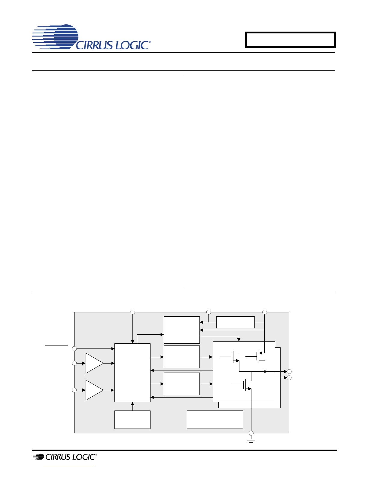
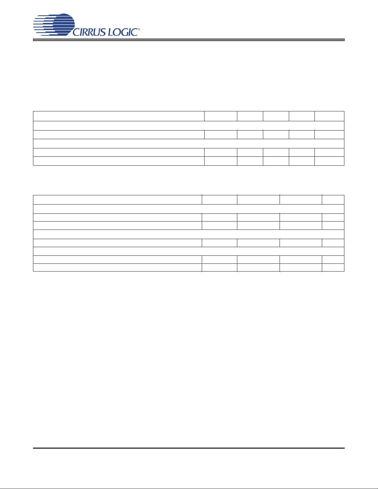
Gate Drivers
Class-H
Controller
Advanced ΔΣ
Modulator
Gate Drivers
Internal
Oscillator
Gain
Gain
Audio In +
Audio In -
Shutdown
Speaker Out +
Speaker Out -
GND
VBATT
2.5V - 5V
LDO Filter
Short C ircuit/ Thermal
Protect ion
MODE
Low Drop-Out
Voltage Regulator
CS35L01/03
3.0 W Mono Class-D Audio Amplifier with Low Idle Current
CS35L01 and CS35L03 Features
Filterless Hybrid Class-D Architecture
– <1 mA Quiescent Current
– 1 x 3.0 W into 4 (10% THD+N)
– 1 x 2.4 W into 4 (1% THD+N)
– 1 x 1.7 W into 8 (10% THD+N)
– 1 x 1.4 W into 8 (1% THD+N)
Advanced Closed-loop Modulation
– 98 dB Signal-to-Noise Ratio (A-Weighted)
– 0.02% THD+N @ 1 W (SD & HD Mode)
Integrated Protection and Automatic Recovery
for Output Short-circuit and Thermal Overload
Pin-compatible 9-ball WLCSP family for easy
upgrade path
– CS35L01: +6 dB default Gain
– CS35L03: +12 dB default Gain
Pop and Click Suppression
Common Applications
Mobile Phones
Laptops/Netbooks/Tablets
Portable Navigation Devices
Active Speakers
Portable Gaming
General Description
The CS35L01 and the CS35L03 are 3.0W high efficiency Hybrid Class-D audio amplifiers with low idle current
consumption.
The CS35L01/03 features an advanced closed-loop architecture to provide 0.02% THD+N at 1 W and -87 dB
PSRR at 217 Hz.
A flexible Hybrid Class-D output stage offers four
modes of operation: Standard Class-D (SD) mode offers full audio bandwidth and high audio performance;
Hybrid Class-D (HD) mode offers a substantial reduction in idle power consumption with an integrated ClassH controller; Reduced Frequency Class-D (FSD) mode
reduces the output switching frequency, producing lower electromagnetic interference (EMI); and Reduced
Frequency Hybrid Class-D (FHD) mode produces both
the lower idle power consumption of HD mode and the
reduced EMI benefits of FSD mode.
Requiring minimal external components and PCB
space, the CS35L01 and CS35L03 are available in a
1.2 mm x 1.2 mm, 9-ball WLCSP package in Commercial grade (-10°C to +70°C). Please see “Ordering
Information” on page 33 for package options and gain
configurations.
http://www.cirrus.com
Copyright Cirrus Logic, Inc. 2011
(All Rights Reserved)
JULY '11
DS909F1
Page 2

TABLE OF CONTENTS
1. BALL DESCRIPTIONS FOR CS35L01 & CS35L03 .............................................................................. 5
2. DIGITAL BALL CONFIGURATIONS ..................................................................................................... 6
3. TYPICAL CONNECTION DIAGRAMS ................................................................................................... 7
4. CHARACTERISTICS & SPECIFICATIONS ........................................................................................... 8
5. APPLICATIONS ................................................................................................................................... 15
5.1 MODE Descriptions ....................................................................................................................... 15
5.2 Reducing the Gain with External Series Resistors ........................................................................ 16
5.3 Output Filtering with the CS35L01/03 ............................................................................................ 17
5.4 Power-Up and Power-Down .......................................................................................................... 19
5.5 Over Temperature Protection ........................................................................................................ 20
6. TYPICAL PERFORMANCE PLOTS ..................................................................................................... 21
6.1 SD Mode Typical Performance Plots ............................................................................................. 21
6.2 FSD Mode Typical Performance Plots ........................................................................................... 23
6.3 HD Mode Typical Performance Plots ............................................................................................. 25
6.4 FHD Mode Typical Performance Plots ........................................................................................... 27
7. PARAMETER DEFINITIONS ................................................................................................................ 29
8. PACKAGING AND THERMAL INFORMATION .................................................................................. 30
8.1 Package Drawings and Dimensions (Note 20) .............................................................................. 30
8.2 Recommend PCB Footprint and Routing Configuration ................................................................ 31
8.3 Package Thermal Performance ..................................................................................................... 31
9. ORDERING INFORMATION ................................................................................................................ 33
10. REVISION HISTORY .......................................................................... ... .... ... ... ... .... ... ... ... ................... 33
CS35L01/03
2 DS909F1
Page 3

CS35L01/03
LIST OF FIGURES
Figure 1. Top View of WLCSP Pinout (Looking down through die) . . . . . . . . . . . . . . . . . . . . . . . . . . . . . . . . . . . . 5
Figure 2. Typical Connection Diagram for SD & FSD Mode . . . . . . . . . . . . . . . . . . . . . . . . . . . . . . . . . . . . . . . . . . 7
Figure 3. Typical Connection Diagram for HD & FHD Mode . . . . . . . . . . . . . . . . . . . . . . . . . . . . . . . . . . . . . . . . . . 7
Figure 4. Adjusting Gain via External Series Resistance . . . . . . . . . . . . . . . . . . . . . . . . . . . . . . . . . . . . . . . . . . . 16
Figure 5. Optional Output Filter Components . . . . . . . . . . . . . . . . . . . . . . . . . . . . . . . . . . . . . . . . . . . . . . . . . . . . 17
Figure 6. Power-Up Timing with Input Zero-Crossing . . . . . . . . . . . . . . . . . . . . . . . . . . . . . . . . . . . . . . . . . . . . . . 19
Figure 7. Power Up Timing without Input Zero-Crossing . . . . . . . . . . . . . . . . . . . . . . . . . . . . . . . . . . . . . . . . . . . 19
Figure 8. THD+N vs. Output Power - SD Mode R
Figure 9. THD+N vs. Output Power - SD Mode R
Figure 10. THD+N vs. Frequency - SD Mode VBATT = 5.0 V . . . . . . . . . . . . . . . . . . . . . . . . . . . . . . . . . . . . . . . 21
Figure 11. THD+N vs. Frequency - SD Mode VBATT = 4.2 V . . . . . . . . . . . . . . . . . . . . . . . . . . . . . . . . . . . . . . . 21
Figure 12. THD+N vs. Frequency - SD Mode VBATT = 3.7 V . . . . . . . . . . . . . . . . . . . . . . . . . . . . . . . . . . . . . . . 21
Figure 13. Frequency Response - SD Mode . . . . . . . . . . . . . . . . . . . . . . . . . . . . . . . . . . . . . . . . . . . . . . . . . . . . . 21
Figure 14. Idle Current Draw vs. VBATT - SD Mode R
Figure 15. Output Power vs. VBATT - SD Mode . . . . . . . . . . . . . . . . . . . . . . . . . . . . . . . . . . . . . . . . . . . . . . . . . . 22
Figure 16. Efficiency vs. Output Power - SD Mode R
Figure 17. Efficiency vs. Output Power - SD Mode R
Figure 18. Supply Current vs. Output Power - SD Mode R
Figure 19. Supply Current vs. Output Power - SD Mode R
Figure 20. THD+N vs. Output Power - FSD Mode R
Figure 21. THD+N vs. Output Power - FSD Mode R
Figure 22. THD+N vs. Frequency - FSD Mode VBATT = 5.0 V . . . . . . . . . . . . . . . . . . . . . . . . . . . . . . . . . . . . . . 23
Figure 23. THD+N vs. Frequency - FSD Mode VBATT = 4.2 V . . . . . . . . . . . . . . . . . . . . . . . . . . . . . . . . . . . . . . 23
Figure 24. THD+N vs. Frequency - FSD Mode VBATT = 3.7 V . . . . . . . . . . . . . . . . . . . . . . . . . . . . . . . . . . . . . . 23
Figure 25. Frequency Response - FSD Mode . . . . . . . . . . . . . . . . . . . . . . . . . . . . . . . . . . . . . . . . . . . . . . . . . . . 23
Figure 26. Idle Current Draw vs. VBATT - FSD Mode R
Figure 27. Output Power vs. VBATT - FSD Mode . . . . . . . . . . . . . . . . . . . . . . . . . . . . . . . . . . . . . . . . . . . . . . . . 24
Figure 28. Efficiency vs. Output Power - FSD Mode R
Figure 29. Efficiency vs. Output Power - FSD Mode R
Figure 30. Supply Current vs. Output Power - FSD Mode R
Figure 31. Supply Current vs. Output Power - FSD Mode R
Figure 32. THD+N vs. Output Power - HD Mode R
Figure 33. THD+N vs. Output Power - HD Mode R
Figure 34. THD+N vs. Frequency - HD Mode VBATT = 5.0 V . . . . . . . . . . . . . . . . . . . . . . . . . . . . . . . . . . . . . . . 25
Figure 35. THD+N vs. Frequency - HD Mode VBATT = 4.2 V . . . . . . . . . . . . . . . . . . . . . . . . . . . . . . . . . . . . . . . 25
Figure 36. THD+N vs. Frequency - HD Mode VBATT = 3.7 V . . . . . . . . . . . . . . . . . . . . . . . . . . . . . . . . . . . . . . . 25
Figure 37. Frequency Response- HD Mode . . . . . . . . . . . . . . . . . . . . . . . . . . . . . . . . . . . . . . . . . . . . . . . . . . . . . 25
Figure 38. Idle Current Draw vs. VBATT - HD Mode R
Figure 39. Output Power vs. VBATT - HD Mode . . . . . . . . . . . . . . . . . . . . . . . . . . . . . . . . . . . . . . . . . . . . . . . . . 26
Figure 40. Efficiency vs. Output Power - HD Mode R
Figure 41. Efficiency vs. Output Power - HD Mode R
Figure 42. Supply Current vs. Output Power - HD Mode R
Figure 43. Supply Current vs. Output Power - HD Mode R
Figure 44. THD+N vs. Output Power - FHD Mode R
Figure 45. THD+N vs. Output Power - FHD Mode R
Figure 46. THD+N vs. Frequency - FHD Mode VBATT = 5.0 V . . . . . . . . . . . . . . . . . . . . . . . . . . . . . . . . . . . . . . 27
Figure 47. THD+N vs. Frequency - FHD Mode VBATT = 4.2 V . . . . . . . . . . . . . . . . . . . . . . . . . . . . . . . . . . . . . . 27
Figure 48. THD+N vs. Frequency - FHD Mode VBATT = 3.7 V . . . . . . . . . . . . . . . . . . . . . . . . . . . . . . . . . . . . . . 27
Figure 49. Frequency Response - FHD Mode . . . . . . . . . . . . . . . . . . . . . . . . . . . . . . . . . . . . . . . . . . . . . . . . . . . 27
Figure 50. Idle Current Draw vs. VBATT - FHD Mode R
Figure 51. Output Power vs. VBATT - FHD Mode . . . . . . . . . . . . . . . . . . . . . . . . . . . . . . . . . . . . . . . . . . . . . . . . 28
Figure 52. Efficiency vs. Output Power - FHD Mode R
= 8 W . . . . . . . . . . . . . . . . . . . . . . . . . . . . . . . . . . . . . . . . . . 21
L
= 4 W . . . . . . . . . . . . . . . . . . . . . . . . . . . . . . . . . . . . . . . . . . 21
L
=8W+33mH (Note 16) . . . . . . . . . . . . . . . . . . . . . . . 22
L
= 8 W + 33 mH . . . . . . . . . . . . . . . . . . . . . . . . . . . . . . . . 22
L
= 4 W + 33 mH . . . . . . . . . . . . . . . . . . . . . . . . . . . . . . . . 22
L
L
L
= 8 W . . . . . . . . . . . . . . . . . . . . . . . . . . . . . . . . . . . . . . . . . 25
L
= 4 W . . . . . . . . . . . . . . . . . . . . . . . . . . . . . . . . . . . . . . . . . 25
L
L
L
L
L
= 8 W + 33 mH . . . . . . . . . . . . . . . . . . . . . . . . . . . . 22
L
= 4 W + 33 mH . . . . . . . . . . . . . . . . . . . . . . . . . . . . 22
L
= 8 W . . . . . . . . . . . . . . . . . . . . . . . . . . . . . . . . . . . . . . . . 23
= 4 W . . . . . . . . . . . . . . . . . . . . . . . . . . . . . . . . . . . . . . . . 23
=8W+33mH (Note 17) . . . . . . . . . . . . . . . . . . . . . . 24
L
= 8 W + 33 mH . . . . . . . . . . . . . . . . . . . . . . . . . . . . . . . 24
L
= 4 W + 33 mH . . . . . . . . . . . . . . . . . . . . . . . . . . . . . . . 24
L
L
= 8 W + 33 mH . . . . . . . . . . . . . . . . . . . . . . . . . . . 24
L
= 4 W + 33 mH . . . . . . . . . . . . . . . . . . . . . . . . . . . 24
L
=8W+33mH (Note 18) . . . . . . . . . . . . . . . . . . . . . . . 26
= 8 W + 33 mH . . . . . . . . . . . . . . . . . . . . . . . . . . . . . . . . 26
= 4 W + 33 mH . . . . . . . . . . . . . . . . . . . . . . . . . . . . . . . . 26
= 8 W + 33 mH . . . . . . . . . . . . . . . . . . . . . . . . . . . . 26
L
= 4 W + 33 mH . . . . . . . . . . . . . . . . . . . . . . . . . . . . 26
L
= 8 W . . . . . . . . . . . . . . . . . . . . . . . . . . . . . . . . . . . . . . . . 27
= 4 W . . . . . . . . . . . . . . . . . . . . . . . . . . . . . . . . . . . . . . . . 27
=8W+33mH (Note 19) . . . . . . . . . . . . . . . . . . . . . . 28
L
= 8 W + 33 mH . . . . . . . . . . . . . . . . . . . . . . . . . . . . . . . 28
L
DS909F1 3
Page 4

CS35L01/03
Figure 53. Efficiency vs. Output Power - FHD Mode R
Figure 54. Supply Current vs. Output Power - FHD Mode R
Figure 55. Supply Current vs. Output Power - FHD Mode R
= 4 W + 33 mH . . . . . . . . . . . . . . . . . . . . . . . . . . . . . . . 28
L
= 8 W + 33 mH . . . . . . . . . . . . . . . . . . . . . . . . . . . 28
L
= 4 W + 33 mH . . . . . . . . . . . . . . . . . . . . . . . . . . . 28
L
LIST OF TABLES
Table 1. LFILT+ and MODE Operation Configurations . . . . . . . . . . . . . . . . . . . . . . . . . . . . . . . . . . . . . . . . . . . . . 15
Table 2. JA Specification for Typical PCB Designs . . . . . . . . . . . . . . . . . . . . . . . . . . . . . . . . . . . . . . . . . . . . . . . 31
4 DS909F1
Page 5
1. BALL DESCRIPTIONS FOR CS35L01 & CS35L03
A1
IN+
A2
MODE
A3
OUT-
B1
LFILT +
B2
VBATT
B3
GND
C1
IN-
C2
SD
C3
OUT+
Figure 1. Top View of WLCSP Pinout
(Looking down through die)
CS35L01/03
Ball Name
IN+ A1 Positive Analog Input (Input) - Differential positive audio signal input.
MODE A2 Switching Mode (Input) - Controls the output switching modes of the CS35L01/03.
OUT- A3 Negative PWM Output (Output) - Differential negative PWM output.
LFILT+ B1
VBATT B2 Positive Analog Power Supply (Input) - Positive power supply input.
GND B3 Ground (Input) - Power supply ground.
IN- C1 Negative Analog Input (Input) - Differential negative audio signal input.
SD
OUT+ C3 Positive PWM Output (Output) - Differential Positive PWM output.
#
Description
Low Drop Out Regulator Filter (Output) - Bypass capacitor connection point for internal LDO. Con-
necting this net to VBATT places the device into SD mode.
C2 Shutdown (Input) - Pulling this net low places the CS35L01/03 in shutdown.
DS909F1 5
Page 6
CS35L01/03
2. DIGITAL BALL CONFIGURATIONS
See (Note 1) and (Note 2) below the table.
Power Supply I/O Name Ball Direction Internal Connections Configuration
C2 Input No Internal Pull Up Hysteresis on CMOS Input
VBATT
Note:
1. Refer to specification table “Digital Interface Specifications and Characteristics” on page 14 for details
on the digital I/O characteristics.
2. I/O voltage levels must not exceed the voltage listed in table “Absolute Maximum Ratings” on page 8.
SD
MODE A2 Input No Internal Pull Up Hysteresis on CMOS Input
6 DS909F1
Page 7
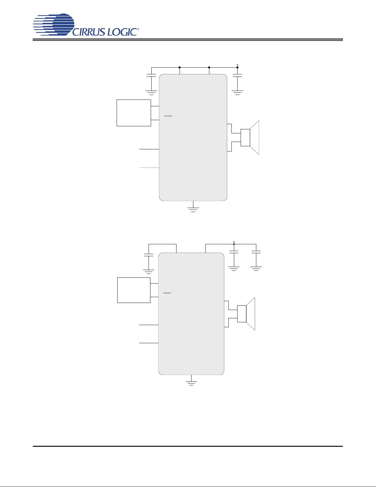
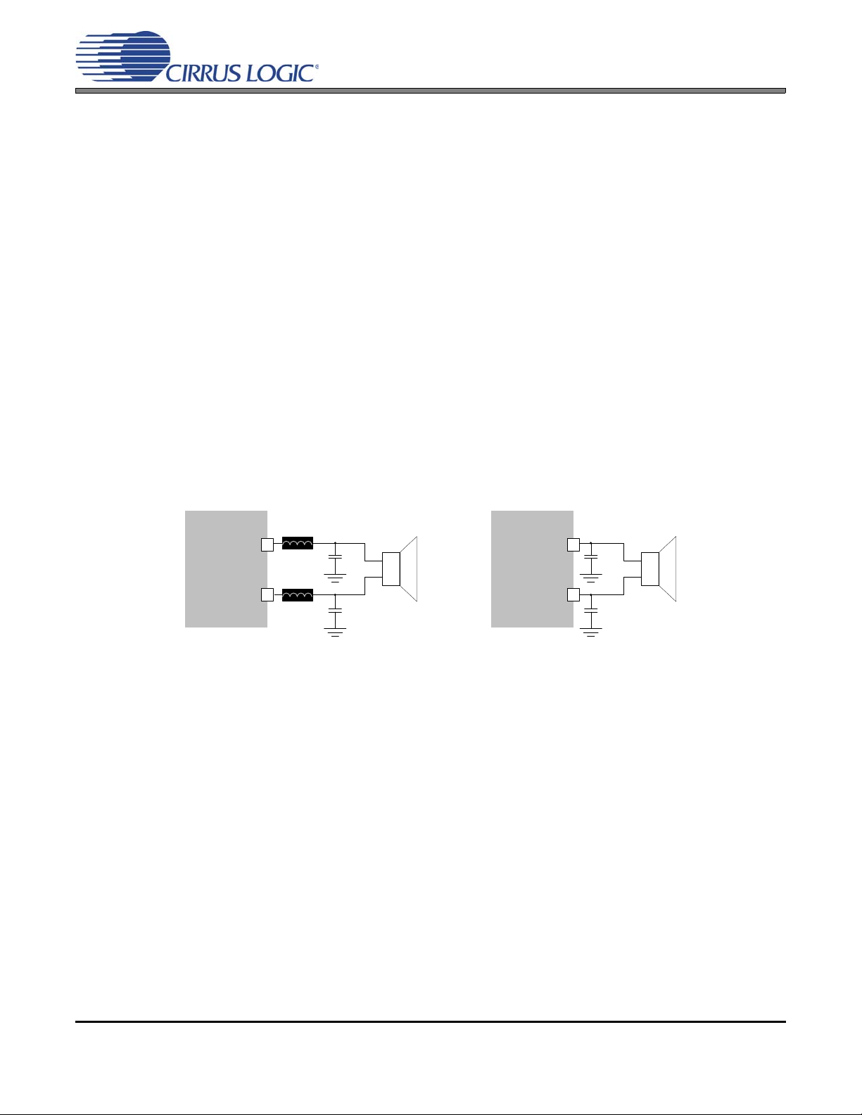
3. TYPICAL CONNECTION DIAGRAMS
Audio In+
Audio In-
System
Controller
GND
AIN+
AIN+
MODE
OUT+
OUT-
2.5V - 5V
VBATTLFILT+
10uF0. 1uF
SD
1uF
0.1uF
2.5V - 5 V
10u F
Audio In+
Audio In-
System
Controller
GND
AIN+
AIN+
MODE
OUT+
OUT-
VBATTLFILT+
SD
(Note 3)
CS35L01/03
Note:
Figure 2. Typical Connection Diagram for SD & FSD Mode
3. The value of the capacitance connected to the LFILT+ net should not exceed 4.7 F. Presence of a
capacitance above 4.7 F will prevent proper HD and FHD operation.
Figure 3. Typical Connection Diagram for HD & FHD Mode
DS909F1 7
Page 8
CS35L01/03
4. CHARACTERISTICS & SPECIFICATIONS
Test Conditions (unless otherwise specified): GND = 0 V; All voltages with respect to ground; Input signal = 997 Hz
differential sine wave; T
= 25°C; VBATT = 5.0 V; RL=8; 22 Hz to 20 kHz measurement bandwidth; Measure-
A
ments taken with AES17 measurement filter and Audio Precision AUX-0025 passive filter.
RECOMMENDED OPERATING CONDITIONS
GND = 0 V; All voltages with respect to ground. Please see (Note 4).
Parameters Symbol Min Typ Max Units
DC Power Supply
Supply Voltage VBATT 2.5 5.0 5.5 V
Temperature
Ambient Temperature T
Junction Temperature T
A
J
-10 - +70 °C
-10 - +150 °C
ABSOLUTE MAXIMUM RATINGS
GND = 0 V; All voltages with respect to ground.
Parameters Symbol Min Max Units
DC Power Supply
Supply Voltage VBATT -0.3 6.0 V
LFILT+ Current (Note 5) I
VDREG
Inputs
Input Current I
in
Temperature
Ambient Operating Temperature (power applied) T
Storage Temperature T
A
stg
WARNING:Operation at or beyond these limits may result in permanent damage to the device.
-10A
-±10mA
-20 +125 °C
-65 +150 °C
Notes:
4. Functionality is not guaranteed or implied outside of these limits. Operation outside of these limits may
adversely affect device reliability.
5. No external loads should be connected to the LFILT+ net. Any connection of a load to this point may
result in errant operation or performance degradation in the device.
8 DS909F1
Page 9
ELECTRICAL CHARACTERISTICS - ALL OPERATIONAL MODES
Parameters Symbol Test Conditions Min Typ Max Units
Max. Current from LFILT+ (Note 6)
LFILT+ Output Impedance Z
VBATT Limit for HD/FHD Mode (Note 7)
Input Level for Entering LDO Operation in
HD/FHD Modes (Note 8)
Input Level for Entering VBATT Operation in
HD/FHD Modes (Note 9)
I
LFILT+
LFILT+
VB
V
IN-LDO
V
IN-VBATT
LIM
CS35L03
CS35L01
CS35L03
CS35L01
-10 -A
-0.7 -
-3.0 -VDC
--0.015•VBATT
0.029•VBATT--
-
-
0.09
0.19
CS35L01/03
Vrms
Vrms
--Vrms
Vrms
LDO Entry Time Delay
LDO Level for HD/FHD Modes
Output Offset Voltage
t
LDO
V
V
OFFSET
Amplifier Gain
Shutdown Supply Current I
MOSFET On Resistance R
Thermal Error Threshold (Note 10)
Thermal Error Retry Time (Note 10)
Under Voltage Lockout Threshold (Note 11)
A(SD)
DS(ON)
T
R
UVLO - 2.0 - V
Operating Efficiency
LDO
Inputs AC coupled to GND
CS35L03
A
V
CS35L01
SD = Low
I
= 0.5 A
bias
TE
TE
Output Levels at 10% THD+N
VBATT = 5 VDC - 92 - %
Load
VBATT = 3.7 VDC - 91 - %
8 + 33H
VBATT = 5 VDC - 87 - %
Load
VBATT = 3.7 VDC - 86 - %
4 + 33H
- 1200 - ms
-1.0 -V
-+/-1.5 -mV
-
-
12
--dB
6
dB
-0.05 -A
-270 -m
-150 -C
-100 -ms
Note:
6. No external loads should be connected to the LFILT+ net. Any connection of a load to this point may
result in errant operation or performance degradation in the device.
7. When VBATT is below this threshold (VB
), operation is automatically restricted to SD mode.
LIM
8. When operating in HD or FHD mode and the differential input voltage remains below the input level
threshold (V
) for a period of time (t
IN-LDO
), the PWM outputs will be powered by the internally
LDO
generated LDO supply (VLDO).
9. When operating in HD or FHD mode and the differential input voltage is above this input level
threshold (V
IN-VBATT
), the PWM outputs will be powered directly from the VBATT supply.
10. Refer to Section 5.5 for more information on Thermal Error functionality.
11. Under Voltage Lockout is the threshold at which a decreasing VBATT supply will disable device
operation.
DS909F1 9
Page 10
ELECTRICAL CHARACTERISTICS - SD MODE
Parameters Symbol Test Conditions Min Typ Max Units
THD+N = 1%
= 8 (VBATT = 5.0/4.2/3.7 VDC)
R
L
Output Power
(Continuous Average)
Total Harmonic Distortion + Noise THD+N
Power Supply Rejection Ratio PSRR
RL = 4 (VBATT = 5.0/4.2/3.7 VDC)
P
O
THD+N = 10%
= 8 (VBATT = 5.0/4.2/3.7 VDC)
R
L
= 4 (VBATT = 5.0/4.2/3.7 VDC)
R
L
PO = 1.0 W
V
= 200 mVPP, AINx AC coupled to GND
ripple
@ 217 Hz
@ 1 kHz
CS35L01/03
-
1.39/0.98/0.76
-
2.41/1.69/1.30
-
1.73/1.23/0.95
-
3.03/2.12/1.64
-0.02 -%
-
-
87
82
-
W
W
-
W
W
-
dB
-
dB
Common-Mode Rejection Ratio CMRR
V
ripple
=1VPP, f
ripple
= 217 Hz
-73 -dB
Inputs AC Coupled to Ground,
Signal to Noise Ratio
A-Weighted
SNR
Referenced to 1% THD+N (Note 13)
A
CS35L03
CS35L01
-
-
96
97
-
dB
-
dB
AIN+ connected to AIN-
Idle Channel Noise
A-Weighted
ICN
A
CS35L03
CS35L01
-
-
54
49
--Vrms
Vrms
AIN+ connected to AIN-
Idle Channel Noise ICN
CS35L03
CS35L01
-
-
110
100
--Vrms
Vrms
Frequency Response FR 20 Hz to 20 kHz -0.1 0 0.4 dB
Total Group Delay GD - 6 - s
Output Switching Frequency
f
sw1
-192 -kHz
AIN+ connected to AIN-, No Output Load
Idle Current Draw (Note 12) I
Input Impedance, Single Ended
VBATT = 5.0 VDC
IDLE
VBATT = 4.2 VDC
VBATT = 3.7 VDC
CS35L03
Z
IN
CS35L01
-
-
-
-
-
1.40
1.28
1.21
65
100
-
mA
-
mA
-
mA
-
k
-
k
RL = 8 (VBATT = 5.0/4.2/3.7 VDC)
Input Voltage @ 1 % THD+N V
ICLIP
CS35L03
CS35L01
--0.85/0.72/0.63
1.71/1.44/1.26--
Vrms
Vrms
10 DS909F1
Page 11

ELECTRICAL CHARACTERISTICS - FSD MODE
Parameters Symbol Test Conditions Min Typ Max Units
THD+N = 1%
= 8 (VBATT = 5.0/4.2/3.7 VDC)
R
L
Output Power
(Continuous Average)
Total Harmonic Distortion + Noise THD+N
Power Supply Rejection Ratio PSRR
RL = 4 (VBATT = 5.0/4.2/3.7 VDC)
P
O
THD+N = 10%
= 8 (VBATT = 5.0/4.2/3.7 VDC)
R
L
= 4 (VBATT = 5.0/4.2/3.7 VDC)
R
L
PO = 1.0 W - 0.10 - %
V
= 200 mVPP, AINx AC coupled to GND
ripple
@ 217 Hz
@ 1 kHz
-
1.32/0.94/0.72
-
2.30/1.62/1.24
-
1.70/1.21/0.94
-
2.94/2.08/1.61
-
-
CS35L01/03
-
-
-
-
88
81
-
-
W
W
W
W
dB
dB
Common-Mode Rejection Ratio CMRR
V
ripple
=1VPP, f
ripple
=217Hz
-71 -dB
Inputs AC Coupled to Ground,
Signal to Noise Ratio
A-Weighted
SNR
Referenced to 1% THD+N (Note 13)
A
CS35L03
CS35L01
-
-
80
80
-
dB
-
dB
AIN+ connected to AIN-
Idle Channel Noise
A-Weighted
ICN
A
CS35L03
CS35L01
-
-
300
290
--Vrms
Vrms
AIN+ connected to AIN-
Idle Channel Noise ICN
CS35L03
CS35L01
-
-
570
550
--Vrms
Vrms
Frequency Response FR 20 Hz to 20 kHz -4.0 0 0.5 dB
Total Group Delay GD - 14 - s
Output Switching Frequency
f
sw2
- 76 - kHz
AIN+ connected AIN-, No Output Load
Idle Current Draw (Note 12) I
Input Impedance, Single Ended
IDLE
Z
IN
VBATT = 5.0 VDC
VBATT = 4.2 VDC
VBATT = 3.7 VDC
CS35L03
CS35L01
-
-
-
-
-
1.04
0.98
0.95
160
240
-
mA
-
mA
-
mA
--k
k
RL = 8 (VBATT = 5.0/4.2/3.7 VDC)
Input Voltage @ 1 % THD+N V
ICLIP
CS35L03
CS35L01
--0.83/0.70/0.61
1.66/1.39/1.22--
Vrms
Vrms
Note:
12. Idle Current Draw (I
) is specified without any output filtering. Refer to Section 5.3 on page 17 for
IDLE
information on output filtering.
DS909F1 11
Page 12

ELECTRICAL CHARACTERISTICS - HD MODE
Parameters Symbol Test Conditions Min Typ Max Units
THD+N = 1%
= 8 (VBATT = 5.0/4.2/3.7 VDC)
R
L
Output Power
(Continuous Average)
Total Harmonic Distortion + Noise THD+N
Power Supply Rejection Ratio PSRR
RL = 4 (VBATT = 5.0/4.2/3.7 VDC)
P
O
THD+N = 10%
= 8 (VBATT = 5.0/4.2/3.7 VDC)
R
L
= 4 (VBATT = 5.0/4.2/3.7 VDC)
R
L
PO = 1.0 W - 0.02 - %
V
= 200 mVPP, AINx AC coupled to GND
ripple
@ 217 Hz
@ 1 kHz
-
1.39/0.99/0.76
-
2.41/1.69/1.30
-
1.73/1.23/0.95
-
3.03/2.13/1.64
-
-
CS35L01/03
-
-
-
-
89
86
-
-
W
W
W
W
dB
dB
Common-Mode Rejection Ratio CMRR
V
ripple
=1VPP, f
ripple
= 217 Hz
-73-dB
Inputs AC Coupled to Ground,
Signal to Noise Ratio
A-Weighted
SNR
Referenced to 1% THD+N (Note 13)
A
CS35L03
CS35L01
-
-
97
98
-
dB
-
dB
AIN+ connected to AIN-
Idle Channel Noise
A-Weighted
ICN
A
CS35L03
CS35L01
-
-
49
43
--Vrms
Vrms
AIN+ connected to AIN-
Idle Channel Noise ICN
CS35L03
CS35L01
-
-
86
83
--Vrms
Vrms
Frequency Response FR 20 Hz to 20 kHz -0.1 0 0.4 dB
Total Group Delay GD - 6 - s
Output Switching Frequency
f
sw1
- 192 - kHz
AIN+ connected AIN-, No Output Load
Idle Current Draw (Note 14) I
Input Impedance, Single Ended
VBATT = 5.0 VDC
IDLE
VBATT = 4.2 VDC
VBATT = 3.7 VDC
CS35L03
Z
IN
CS35L01
-
-
-
-
-
1.09
1.04
1.01
65
100
-
mA
-
mA
-
mA
-
k
-
k
RL = 8 (VBATT = 5.0/4.2/3.7 VDC)
Input Voltage @ 1% THD+N V
ICLIP
CS35L03
CS35L01
--0.85/0.72/0.63
1.71/1.44/1.26--
Vrms
Vrms
12 DS909F1
Page 13

ELECTRICAL CHARACTERISTICS - FHD MODE
Parameters Symbol Test Conditions Min Typ Max Units
THD+N = 1%
= 8 (VBATT = 5.0/4.2/3.7 VDC)
R
L
= 4 (VBATT = 5.0/4.2/3.7 VDC)
R
Output Power
(Continuous Average)
P
Total Harmonic Distortion + Noise THD+N
Power Supply Rejection Ratio PSRR
Common-Mode Rejection Ratio CMRR
Signal to Noise Ratio
A-Weighted
SNR
L
O
THD+N = 10%
= 8 (VBATT = 5.0/4.2/3.7 VDC)
R
L
= 4 (VBATT = 5.0/4.2/3.7 VDC)
R
L
P
= 1.0 W - 0.11 - %
O
V
= 200 mVPP, AINx AC coupled to GND
ripple
@ 217 Hz
@ 1 kHz
V
ripple
=1VPP, f
ripple
= 217 Hz
Inputs AC Coupled to Ground,
Referenced to 1% THD+N (Note 13)
A
CS35L03
CS35L01
CS35L01/03
-
1.33/0.94/0.72
-
2.31/1.63/1.23
-
1.71/1.21/0.94
-
2.95/2.09/1.61
-
-
89
85
-71-dB
-
-
93
94
-
W
W
-
W
W
-
dB
-
dB
-
dB
-
dB
Idle Channel Noise
A-Weighted
ICN
A
CS35L03
CS35L01
-
-
71
63
--Vrms
Vrms
AIN+ connected to AIN-
AIN+ connected to AIN-
Idle Channel Noise ICN
CS35L03
CS35L01
-
-
125
115
--Vrms
Vrms
Frequency Response FR 20 Hz to 20 kHz -4.0 0 0.5 dB
Output Switching Frequency
f
LDO Operation - 192 - kHz
sw1
Total Group Delay GD - 14 - s
Output Switching Frequency
f
sw2
VBATT Operation
- 76 - kHz
AIN+ connected AIN-, No Output Load
Idle Current Draw (Note 14) I
Input Impedance, Single Ended
IDLE
Z
IN
VBATT = 5.0 VDC
VBATT = 4.2 VDC
VBATT = 3.7 VDC
CS35L03
CS35L01
-
-
-
-
-
1.09
1.04
1.01
160
240
-
-
-
-
-
RL = 8 (VBATT = 5.0/4.2/3.7 VDC)
Input Voltage @ 1 % THD+N V
ICLIP
CS35L03
CS35L01
--0.83/0.70/0.62
1.66/1.39/1.22--
Vrms
Vrms
Note:
13. SNR
dB is referenced to the output signal amplitude resulting in the specified output power at
A
THD+N < 1 %. See “Parameter Definitions” on page 29 for more information.
14. Idle Current Draw (I
) is specified without any output filtering. Refer to Section 5.3 on page 17 for
IDLE
information on output filtering. At idle, the output devices will switch at the same rate in HD and FHD
mode. FHD only changes the output switching frequency when the input levels are above the “Input
Level for Entering VBATT Operation in HD/FHD Modes (V
IN-VBATT
) given in “Electrical Characteristics
- All Operational Modes” on page 9.
mA
mA
mA
k
k
DS909F1 13
Page 14

DIGITAL INTERFACE SPECIFICATIONS AND CHARACTERISTICS
Parameters Symbol Min Max Units
CS35L01/03
Input Leakage Current I
Input Capacitance -10pF
SD Pulse Width Requirement 1 - ms
Logic I/Os (Applicable to GAIN_SEL, MODE, and SD
High-Level Input Voltage V
Low-Level Input Voltage V
)
in
IH
IL
-±10A
0.7•VBATT - V
- 0.3•VBATT V
POWER-UP & POWER-DOWN CHARACTERISTICS
Parameters Symbol Test Conditions Min Typ Max Units
Start-Up Time (Note 15)
Zero Crossing Power-Up Timeout
Power-Down Time
Note:
15. Start-Up Time (t
start
is ready to activate the PWM outputs. The total power-up time from SD
becoming active will vary based on the input signal, not exceeding the Start-Up Time + Zero Crossing
Power-Up Timeout (t
t
t
timeout
After low-to-high SD pin transition edge
start
No audio input applied
t
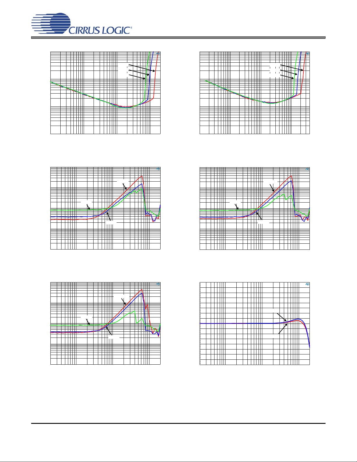
After high-to-low SD pin transition edge
off
) refers to the internal start-up time from when SD is released to when the device
start+ttimeout
). For more information, refer to Section 5.4.
-18-ms
-25-ms
-1-ms
release to the PWM outputs
14 DS909F1
Page 15

5. APPLICATIONS
5.1 MODE Descriptions
The CS35L01/03 devices can be operated in one of four operating modes, determined by the MODE pin
and the LFILT+ pin. The four modes of operation are Standard Class-D operation (SD), Reduced Frequency
Standard Class-D operation (FSD), Hybrid Class-D operation (HD), and Reduced Frequency Hybrid ClassD operation (FHD). Each of these modes can be leveraged to optimize different performance criteria in an
array of applications.
CS35L01/03
MODE connected to:
GND VBATT
VBATT
Filter Cap to Ground
LFILT+ connected to:
Reduced Frequency Class-D Mode
(FSD)
Reduced Frequency Hybrid Class-D Mode
(FHD)
Table 1. LFILT+ and MODE Operation Configurations
5.1.1 Standard Class-D Modes of Operation
5.1.1.1 SD Mode
Standard Class-D (SD) mode supports full audio bandwidth with very good SNR and THD+N performance. This mode of operation is characterized by a traditional closed loop, analog modulated ClassD amplifier. With an output switching frequency of 192 kHz, this mode ensures flat frequency response
across the entire audio frequency range.
5.1.1.2 FSD Mode
The Reduced Frequency Class-D (FSD) mode provides competitive audio performance and a reduction
in radiated emissions by decreasing the switching frequency of the output devices to 76 kHz. This reduction in switching frequency reduces the high-frequency energy being created by the output switching
events. Idle channel noise is slightly higher in this mode of operation than SD mode, with the trade-off
being better EMI performance and power consumption.
Standard Class-D Mode
(SD)
Hybrid Class-D Mode
(HD)
5.1.2 Hybrid Class-D Modes of Operation
Hybrid Class-D and Reduced Frequency Hybrid Class-D modes of operation allows the rail voltage for the
output devices to switch between a high voltage net and a low voltage net depending on the audio content
being amplified. This is explained in more detail in Section 5.1.2.1 and Section 5.1.2.2. Operation in these
modes requires that the voltage present on the VBATT pin be above the level listed as “VBATT Limit for
HD/FHD Mode (VB
and FHD modes of operation of the device will automatically be disabled and operation will be limited to
the SD mode of operation.
DS909F1 15
)” in “Electrical Characteristics - All Operational Modes” on page 9. If it is not, HD
LIM
Page 16
CS35L01/03
Audio In+
Audio In-
R
IN
R
IN
AIN+
AIN-
x
x
Figure 4. Adjusting Gain via External Series Resistance
A
V adjustedAV
20–
Z
IN
Z
INZEXT
+
--------------------------
log=
In both HD and FHD mode, the value of the capacitance connected to the LFILT+ pin must not exceed
4.7 F. If this value is greater than 4.7 F, it will prevent the rail voltage of the output devices from transitioning properly between VBATT and the internal LDO.
5.1.2.1 HD Mode
Hybrid Class-D mode (HD) provides competitive analog performance with a substantial reduction in idle
power dissipation and radiation emissions. In this mode, the output switches at 192 kHz and a secondary
supply is derived from VBATT using an internal 1.0-VDC low drop-out linear regulator (LDO). When the
output signal is at a low amplitude, the Class-D output stage begins to switch from the lower rail voltage
created by the internal LDO. This not only decreases idle power consumption when output capacitors are
used, but also reduces electromagnetic emissions by reducing the amplitude of the square waves being
created at the output of the CS35L01/03 when operating at low amplitude or idle power.
5.1.2.2 FHD Mode
The Reduced Frequency Hybrid Class-D (FHD) mode provides the best overall EMI performance and the
lowest power consumption with slightly decreased frequency response near the top frequency range of
the audio band, for high amplitude signals. In this mode of operation, the output switching frequency is
reduced to 76 kHz during high amplitude transients on the output. The threshold at which this transition
from 192-kHz to 76-kHz switching rate occurs is given as the Input Level Threshold for FHD Operation in
“Electrical Characteristics - FHD Mode” on page 13. Combined with the lower amplitude switching offered
by the Hybrid design, this reduction in switching energy dramatically reduces the emissions levels of the
output stage and its associated components.
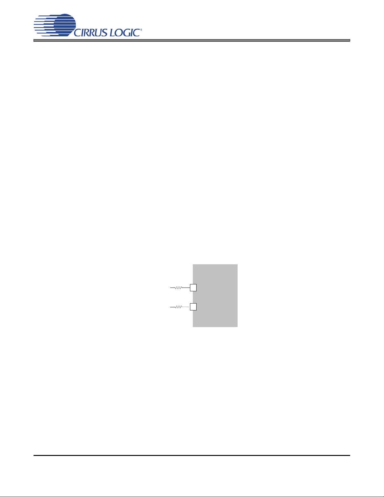
5.2 Reducing the Gain with External Series Resistors
If necessary, it is possible to decrease the gain of the CS35L01/03 by adding series resistors to the audio
input signal as is shown in Figure 4 below.
If input resistors are added, the new gain of the amplifier can be determined by the following equation:
Where:
A
V(adjusted)
Z
= Input impedance of the device being used (See “Electrical Characteristics - SD Mode” on page 10,
IN
“Electrical Characteristics - FSD Mode” on page 11, “Electrical Characteristics - HD Mode” on page 12, or
“Electrical Characteristics - FHD Mode” on page 13 for this value.)
= The new, adjusted gain of the system
Z
= Value of the resistor added in series with the inputs
EXT
16 DS909F1
Page 17
= Original gain of the device being used (See “Electrical Characteristics - All Operational Modes” on
C
FILT
C
FILT
Traditional 2nd Order Optional Filter CS35L01/03’s Minimized Optional Filter
OUT+
OUT-
C
FILT
C
FILT
x
x
L
FILT
L
FILT
OUT+
OUT-
x
x
Figure 5. Optional Output Filter Components
A
V
page 9 for this value.)
5.3 Output Filtering with the CS35L01/03
The CS35L01/03 is specifically designed to minimize radiated electromagnetic interference (EMI) signals.
All of the devices are capable of meeting all stated data sheet performance numbers with no special filtering
required. Additionally, the device has shown to be below the compliance limits of both FCC and CISPR testing with no external filtering required.
Ultimately, compliance with any radiated emissions requirements depends significantly on the entire system
under test. In applications where system-level trade-offs such as compromised component layout or lengthy
speaker wires have increased emissions levels, a passive output filter can be added to the outputs of the
device in order to decrease EMI levels.
5.3.1 Reduced Filter Order with the CS35L01/03
In applications which require an output filter, the unique design of the CS35L01/03 allows a much smaller,
less expensive output filter to be used than what is normally found in Class-D amplifiers. In contrast to a
second order filter implemented with a series inductive element (traditional inductor or ferrite beads) and
a shunt capacitive element, basic filtering for the CS35L01/03 is accomplished by a single-order capacitive element attached to the OUTx terminals. This is highlighted in Figure 5 below. Of course, if the system
requires more aggressive filtering, a ferrite bead can be added in series with the outputs to further attenuate system level noise.
CS35L01/03
5.3.2 Filter Component Selection
Usually, the need for output filtering is determined after the system under test has failed EMI testing. During this testing, problem frequencies are easily identified by the peaks which appear in the spectral plots
gathered in the EMI testing.
Selection of the filter components should ensure that shunt elements (i.e. C
low impedance at the frequency corresponding to the tallest peak in the spectral plot. If needed, series
components such as ferrite beads (i.e. L
ance at the frequency corresponding to the tallest peak in the spectral plot.
Careful attention should be paid to the current-carrying capabilities of any included ferrite beads and the
impedance of the ferrite beads in the audio band. A proper trade-off in ferrite bead selection is one that
allows the ferrite bead to sufficiently attenuate the problematic high-frequency emissions without compromising audio performance.
DS909F1 17
in Figure 5) should be chosen to present a very high imped-
FILT
in Figure 5) present a very
FILT
Page 18

5.3.3 Output Filter Power Dissipation Considerations
PI2Z=
P
1
2
-- -
CV2f=
In systems without inductive series elements like inductors or ferrite beads, power losses in the output
filter are equal to the switching losses that occur in the system due to the cyclical charging and discharging
of capacitors connected to the amplifier outputs. In systems that require an inductive series element, conducted losses also occurs due to the series impedance added to the output path.
5.3.3.1 Conduction Losses for All modes of Operation
For all modes of operation (SD, FSD, HD, and FHD) of the CS35L01/03, the conduction losses are governed by the equation:
Where:
P = Power dissipated in the series impedance.
I = RMS AC output current
Z = impedance of the series element at the frequency of the AC current
This equation neglects any series impedances presented by the PCB traces or speaker wires in the output
path.
CS35L01/03
5.3.3.2 Switching Losses in SD/FSD Mode
Switching losses in SD/FSD Mode are governed by the equation
Where:
P = Power dissipated in the capacitor (neglecting parasites).
C = Value of filtering capacitor
V = Peak voltage developed across the capacitor
f = Switching frequency of the outputs
These calculations are straightforward, as the peak voltage is simply the voltage level attached to VBATT,
the capacitor is the value of capacitor that has been added for filtering (neglecting parasitic board capacitances), and the frequency is 192 kHz or 76 kHz for SD and FSD, respectively.
5.3.3.3 Switching Losses in HD/FHD.
Many factors affect the switching losses when the device is operated in HD/FHD mode. These factors include the frequency of the content being amplified, the voltage level of VBATT, and the amplitude of the
output signal will factor into both the voltage presented across the capacitors and the frequency at which
the capacitors are charged or discharged.
Static signals (i.e. sine waves at a fixed amplitude) are easier to consider than are dynamic signals (i.e.
musical content), as they are governed by the same equation as that listed in Section 5.3.3.1 and Section
5.3.3.2 on page 18. Modifications to that equation are limited to the voltage term (V) and the frequency
term (f), depending on whether the static input signal amplitude is causing the output devices to switch at
76 kHz or 192 kHz, and to operate off of the VBATT supply or off of the internally generated LDO.
18 DS909F1
Page 19
It is important to note that the HD and FHD modes offer significant improvement over traditional Class-D
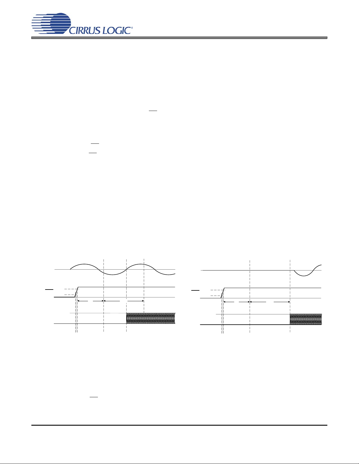
OUT+/-
Shut-Down /
Low Power
Mode
t
start
SD
V
IH
Device Ready:
Waiting for Zero
Crossing Input
Signal or t
timeout
Interna l
Start-Up
V
IL
PWM OUT+/-
Active
VBATT or VLDO
IN+/-
t
timeout
Figure 6. Power-Up Timing with Input
Zero-Crossing
Figure 7. Power Up Timing without Input
Zero-Crossing
OUT+/-
Shut-Down /
Low Power
Mode
t
start
SD
V
IH
Device Ready: Waiting for Zero
Crossing Input Signal or t
timeout
Interna l
Start-Up
V
IL
PWM OUT+/-
Active
VBATT or VLDO
IN+/-
t
timeout
in idle power dissipation when an external output filter is necessary. This is because the voltage term (V)
is significantly reduced in HD and FHD mode. As can be seen in the equation, this is notable because
reduction in the operating voltage reduces power losses not linearly, but instead exponentially- due to the
voltage squared term (V
2
). It is also notable that when operated at high output levels, FHD modes also
offers unique improvement in output filter losses, due to reducing the switching frequency (f) at higher output levels.
5.4 Power-Up and Power-Down
When pulled to a logic low state, the SD pin tristates the outputs and shuts down the CS35L01/03 device,
putting it into a low power mode.
5.4.1 Recommended Power-Up Sequence
1. With the SD pin pulled low, apply power to the CS35L01/03 and wait for the power supply to be stable.
2. Set the SD
pin high to begin normal operation.
5.4.1.1 Zero-Crossing on Power-Up Functionality
The CS35L01/03 implements an input-signal zero-crossing detection function that is enabled during power-up. This function is designed to prevent audible artifacts and eliminate any need to mute the amplifier’s
input audio signal during the power-up process.
CS35L01/03
After a minimum start-up time of t
, the CS35L01/03 will begin to detect input-signal zero-crossings.
start
The amplifier will then enable its switching outputs at the time of the first detected input-signal zero-crossing transition. If no input-signal zero-crossing is detected before t
, the zero-crossing function will tim-
timeout
eout and the outputs will begin switching immediately.
Both t
start
and t
are specified in “Power-Up & Power-Down Characteristics” on page 14.
timeout
5.4.2 Recommended Power-Down Sequence
1. Mute the audio supplied to the CS35L01/03.
2. Pull the SD pin low in order to reset the device and put it into the low power mode.
DS909F1 19
3. The power supply to the CS35L01/03 can now be removed.
Page 20

5.5 Over Temperature Protection
The CS35L01/03 is internally protected against thermal overload. Built in die temperature sensing circuitry
monitors the die temperature and will place the device into shut-down if thermal overload occurs. A thermal overload is characterized by the die temperature reaching the Thermal Error Threshold (T
time the outputs will tristate and shut down.
If the device has entered into shut-down due to a thermal overload, the die temperature must remain below the Thermal Error Threshold (T
order for the device to automatically return to normal operation.
CS35L01/03
) at which
TE
) for the time specified by the Thermal Error Retry Time (RTE) in
TE
Both T
and RTE are specified in “Electrical Characteristics - All Operational Modes” on page 9.
TE
20 DS909F1
Page 21
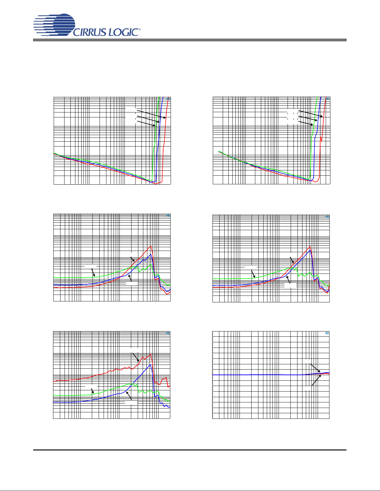
CS35L01/03
0.01
10
0.02
0.05
0.1
0.2
0.5
1
2
5
%
1m 22m 5m 10m 20m 50m 100m 200m 500m 1
W
0.01
10
0.02
0.05
0.1
0.2
0.5
1
2
5
%
1m 42m 5m 10m 20m 50m 100m 200m 500m 1 2
W
Figure 8. THD+N vs. Output Power - SD Mode
R
L
=8
Figure 9. THD+N vs. Output Power - SD Mode
R
L
=4
5.0 V
4.2 V
3.7 V
5.0 V
4.2 V
3.7 V
0.001
10
0.002
0.005
0.01
0.02
0.05
0.1
0.2
0.5
1
2
5
%
20 20k50 100 200 500 1k 2k 5k 10k
Hz
0.001
10
0.002
0.005
0.01
0.02
0.05
0.1
0.2
0.5
1
2
5
%
20 20k50 100 200 500 1k 2k 5k 10k
Hz
Figure 11. THD+N vs. Frequency - SD Mode
VBATT = 4.2 V
1.0 W
0.5 W
0.75 W
0.5 W
0.1 W
0.1 W
Figure 10. THD+N vs. Frequency - SD Mode
VBATT = 5.0 V
-4
+4
-3.5
-3
-2.5
-2
-1.5
-1
-0.5
+0
+0.5
+1
+1.5
+2
+2.5
+3
+3.5
d
B
r
A
20 20k50 100 200 500 1k 2k 5k 10k
Hz
0.001
10
0.002
0.005
0.01
0.02
0.05
0.1
0.2
0.5
1
2
5
%
20 20k50 100 200 500 1k 2k 5k 10k
Hz
Figure 12. THD+N vs. Frequency - SD Mode
VBATT = 3.7 V
Figure 13. Frequency Response - SD Mode
0.625 W
0.1 W
0.5 W
4
8
6. TYPICAL PERFORMANCE PLOTS
Test Conditions (unless otherwise specified): GND = 0 V; All voltages with respect to ground; AV= 6 dB; Input signal = 997 Hz
differential sine wave; T
with AES17 measurement filter and Audio Precision AUX-0025 passive filter.
6.1 SD Mode Typical Performance Plots
= 25°C; VBATT = 5.0 V; RL=8; 10 Hz to 20 kHz Measurement Bandwidth; Measurements taken
A
DS909F1 21
Page 22
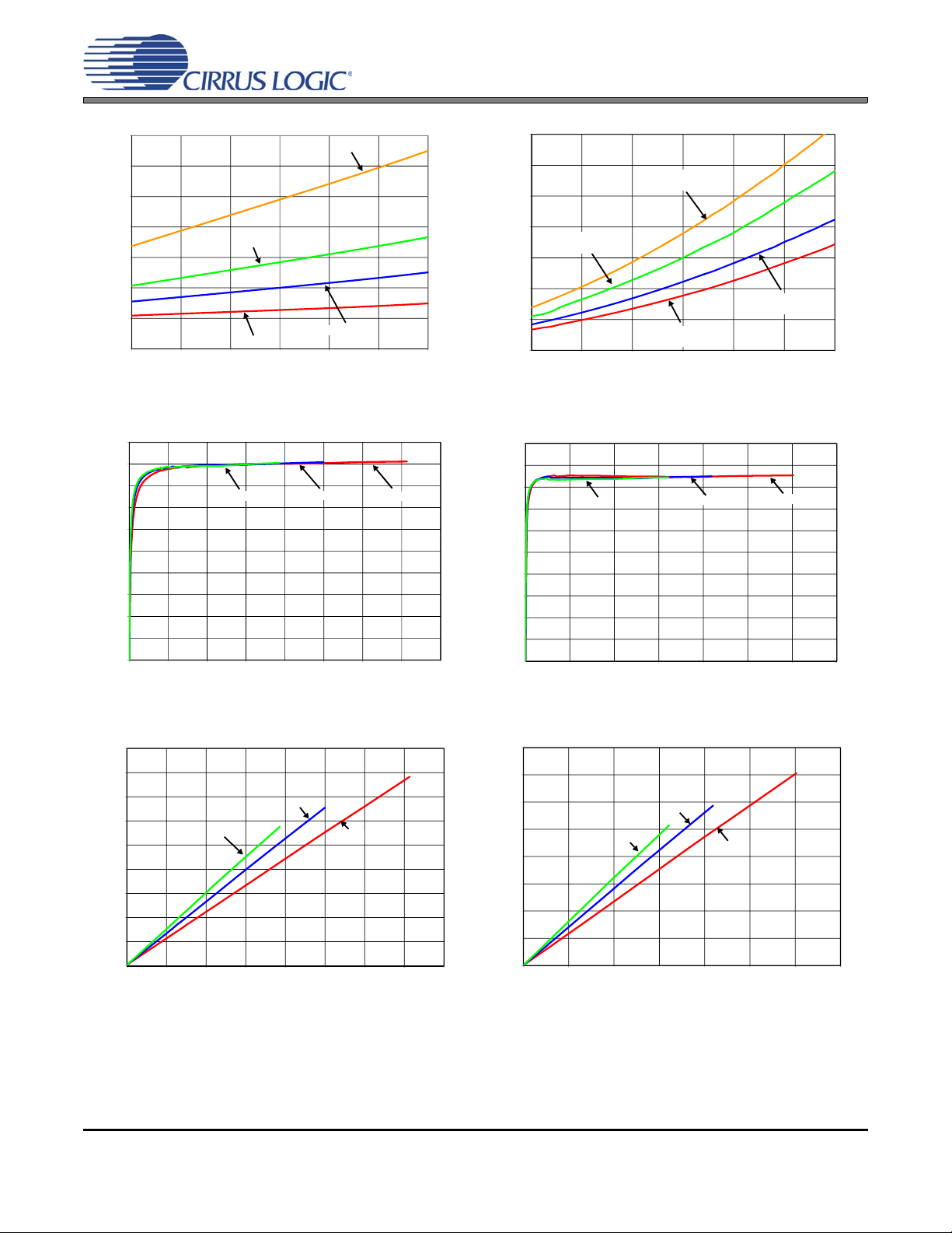
CS35L01/03
0.0
0.5
1.0
1.5
2.0
2.5
3.0
3.5
2.5 3.0 3.5 4.0 4.5 5.0 5.5
Output Power (W)
VBATT Supply Voltage (V)
0.00
1.00
2.00
3.00
4.00
5.00
6.00
7.00
2.533.544.555.5
Idle Current Draw (mA)
VBATT Supply Voltage (V)
Figure 14. Idle Current Draw vs. VBATT - SD Mode
RL=8 +33H (Note 16)
Figure 15. Output Power vs. VBATT - SD Mode
RL = 8
1% THD+N Ratio
RL = 8
10% THD+N Ratio
RL = 4
1% THD+N Ratio
RL = 4
10% THD+N Ratio
No Filter
470 pF
1000 pF
2200 pF
Figure 16. Efficiency vs. Output Power - SD Mode
R
L
=8 +33H
Figure 17. Efficiency vs. Output Power - SD Mode
R
L
=4 +33H
4.2 V
3.7 V
4.2 V
3.7 V
5.0 V
5.0 V
0
50
100
150
200
250
300
350
400
450
0 250 500 750 1000 1250 1500 1750 2000
Current Consumption (mA)
Output Power (mW)
0
100
200
300
400
500
600
700
800
0 500 1000 1500 2000 2500 3000 3500
Current Consumption (mA)
Output Power (mW)
Figure 18. Supply Current vs. Output Power - SD Mode
RL=8 +33H
Figure 19. Supply Current vs. Out put Power - SD Mode
R
L
=4 +33H
5.0 V
4.2 V
3.7 V
5.0 V
4.2 V
3.7 V
100%
90%
80%
70%
60%
50%
Efficiency (%)
40%
30%
20%
10%
0%
0 250 500 750 1000 1250 1500 1750 2000
Output Power (mW)
100%
90%
80%
70%
60%
50%
Efficiency (%)
40%
30%
20%
10%
0%
0 500 1000 1500 2000 2500 3000 3500
Output Power (mW)
Note:
22 DS909F1
16. “Idle Current Draw vs. VBATT - SD Mode” capacitor values refer to C
“CS35L01/03’s Minimized Optional Output Filter,” shown in Figure 5 on page 17.
when configured as the
FILT
Page 23
6.2 FSD Mode Typical Performance Plots
0.01
10
0.02
0.05
0.1
0.2
0.5
1
2
5
%
1m 22m 5m 10m 20m 50m 100m 200m 500m 1
W
0.01
10
0.02
0.05
0.1
0.2
0.5
1
2
5
%
1m 42m 5m 10 m 20m 50m 100m 200m 500m 1 2
W
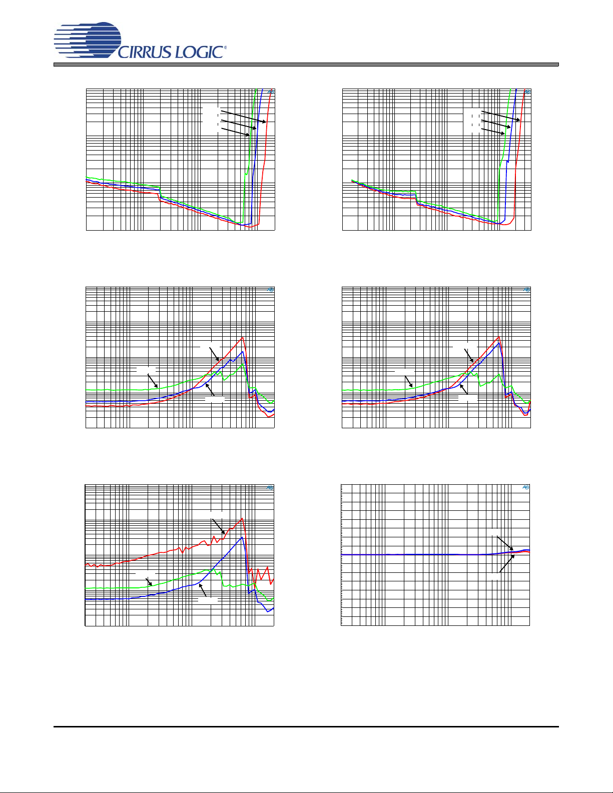
Figure 20. THD+N vs. Output Power - FSD Mode
R
L
=8
Figure 21. THD+N vs. Output Power - FSD Mode
R
L
=4
5.0 V
4.2 V
3.7 V
5.0 V
4.2 V
3.7 V
0.001
10
0.002
0.005
0.01
0.02
0.05
0.1
0.2
0.5
1
2
5
%
20 20k50 100 200 500 1k 2k 5k 10k
Hz
0.001
10
0.002
0.005
0.01
0.02
0.05
0.1
0.2
0.5
1
2
5
%
20 20k50 100 200 500 1k 2k 5k 10k
Hz
Figure 22. THD+N vs. Frequency - FSD Mode
VBATT = 5.0 V
Figure 23. THD+N vs.
Frequency - FSD Mode VBATT = 4.2 V
1.0 W
0.5 W
0.75 W
0.5 W
0.1 W
0.1 W
0.001
10
0.002
0.005
0.01
0.02
0.05
0.1
0.2
0.5
1
2
5
%
20 20k50 100 200 500 1k 2k 5k 10k
Hz
-4
+4
-3.5
-3
-2.5
-2
-1.5
-1
-0.5
+0
+0.5
+1
+1.5
+2
+2.5
+3
+3.5
d
B
r
A
20 20k50 100 200 500 1k 2k 5k 10k
Hz
Figure 24. THD+N vs. Frequency - FSD Mode
VBATT = 3.7 V
Figure 25. Frequency Response - FSD Mode
0.625 W
0.1 W
0.5 W
4
8
CS35L01/03
DS909F1 23
Page 24
CS35L01/03
0.00
0.50
1.00
1.50
2.00
2.50
3.00
3.50
2.5 3 3.5 4 4.5 5 5.5
Idle Current Draw (mA)
VBATT Supply Voltage (V)
0.0
0.5
1.0
1.5
2.0
2.5
3.0
3.5
2.5 3.0 3.5 4.0 4.5 5.0 5.5
Output Power (W)
VBATT Supply Voltage (V)
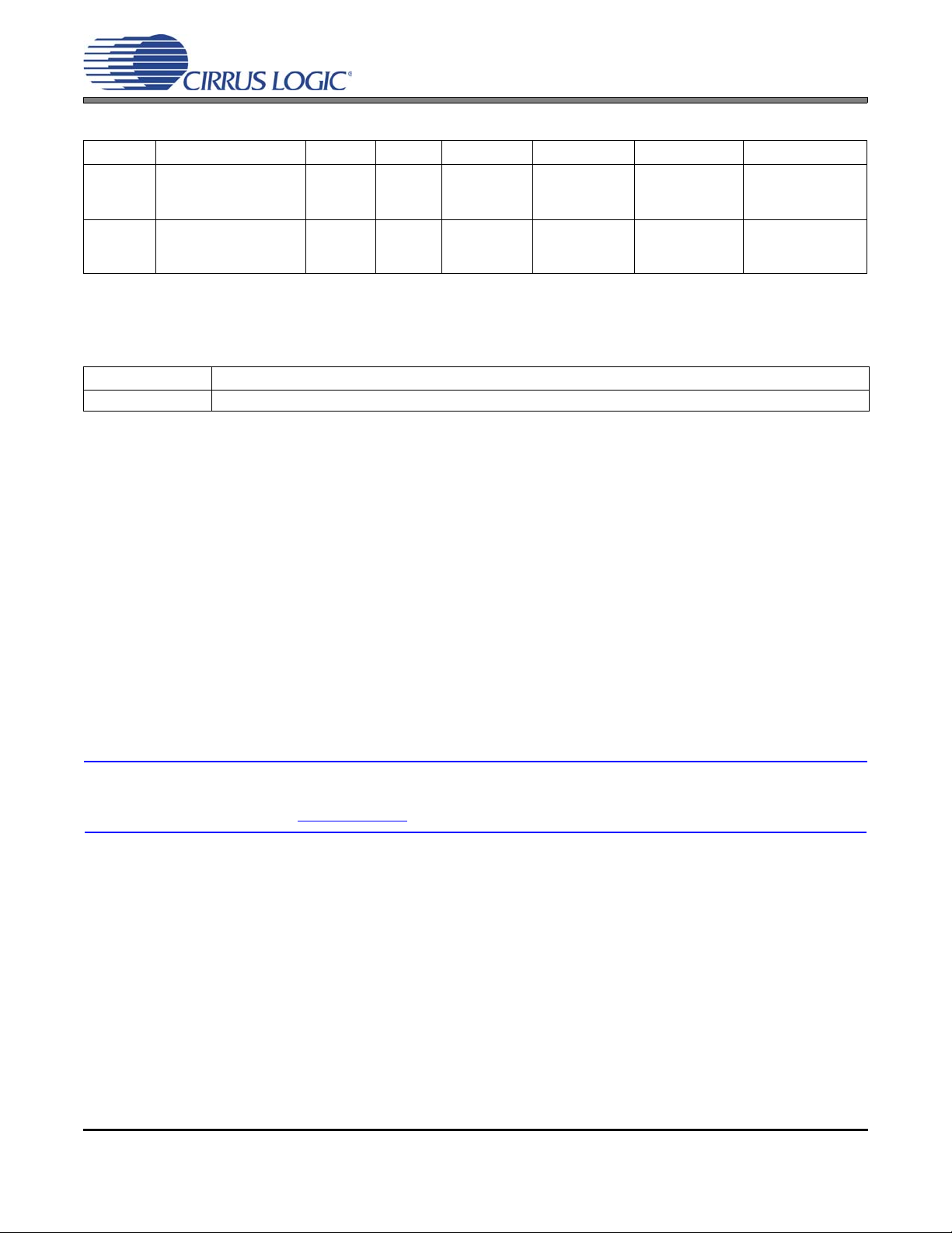
Figure 26. Idle Current Draw vs. VBATT - FSD Mode
R
L
=8 +33H (Note 17)
Figure 27. Output Power vs. VBATT - FSD Mode
RL = 8
1% THD+N Ratio
RL = 8
10% THD+N Ratio
RL = 4
1% THD+N Ratio
RL = 4
10% THD+N Ratio
470 pF
No Filter
1000 pF
2200 pF
0%
10%
20%
30%
40%
50%
60%
70%
80%
90%
100%
0 250 500 750 10 00 1250 1500 17 50 2000
Efficiency (%)
Output Power (mW)
0%
10%
20%
30%
40%
50%
60%
70%
80%
90%
100%
0 500 1000 1500 2000 2500 3000 3500
Efficiency (%)
Output Power (mW)
Figure 28. Efficiency vs. Output Power - FSD Mode
R
L
=8 +33H
Figure 29. Efficiency vs. Output Power - FSD Mode
RL=4 +33H
4.2 V
3.7 V
5.0 V
4.2 V
3.7 V
5.0 V
0
50
100
150
200
250
300
350
400
450
0 250 500 750 1000 1250 1500 1750 2000
Current Consumption (mA)
Output Power (mW)
0
100
200
300
400
500
600
700
800
0 500 1000 1500 2000 2500 3000 3500
Current Consumption (mA)
Output Power (mW)
Figure 30. Supply Current vs. Output Power - FSD Mode
RL=8 +33H
Figure 31. Supply Current vs. Output Powe r - FSD Mode
RL=4 +33H
5.0 V
4.2 V
3.7 V
5.0 V
4.2 V
3.7 V
Note:
24 DS909F1
17. “Idle Current Draw vs. VBATT - FSD Mode” capacitor values refer to C
“CS35L01/03’s Minimized Optional Output Filter”, shown in Figure 5 on page 17.
when configured as the
FILT
Page 25
6.3 HD Mode Typical Performance Plots
0.01
10
0.02
0.05
0.1
0.2
0.5
1
2
5
%
1m 22m 5m 10m 20m 50m 100m 200m 500m 1
W
0.01
10
0.02
0.05
0.1
0.2
0.5
1
2
5
%
1m 42m 5m 10m 20m 50m 100m 200m 500m 1 2
W
Figure 32. THD+N vs. Output Power - HD Mode
RL=8
Figure 33. THD+N vs. Output Power - HD Mode
R
L
=4
5.0 V
4.2 V
3.7 V
5.0 V
4.2 V
3.7 V
0.001
10
0.002
0.005
0.01
0.02
0.05
0.1
0.2
0.5
1
2
5
%
20 20k50 100 200 500 1k 2k 5k 10k
Hz
0.001
10
0.002
0.005
0.01
0.02
0.05
0.1
0.2
0.5
1
2
5
%
20 20k50 100 200 500 1k 2k 5k 10k
Hz
Figure 34. THD+N vs. Frequency - HD Mode
VBATT = 5.0 V
Figure 35. THD+N vs. Frequency - HD Mode
VBATT = 4.2 V
1.0 W
0.5 W
0.75 W
0.5 W
0.1 W
0.1 W
0.001
10
0.002
0.005
0.01
0.02
0.05
0.1
0.2
0.5
1
2
5
%
20 20k50 100 200 500 1k 2k 5k 10k
Hz
-4
+4
-3.5
-3
-2.5
-2
-1.5
-1
-0.5
+0
+0.5
+1
+1.5
+2
+2.5
+3
+3.5
d
B
r
A
20 20k50 100 200 500 1k 2k 5k 10k
Hz
Figure 36. THD+N vs. Frequency - HD Mode
VBATT = 3.7 V
Figure 37. Frequency Response- HD Mode
0.625 W
0.1 W
0.5 W
4
8
CS35L01/03
DS909F1 25
Page 26

CS35L01/03
0.00
0.50
1.00
1.50
2.00
2.50
3.00
3.50
4.00
4.50
2.533.544.555.5
Idle Current Draw (mA)
VBATT Supply Voltage (V)
Figure 38. Idle Current Draw vs. VBATT - HD Mode
R
L
=8 +33H (Note 18)
Figure 39. Output Power vs. VBATT - HD Mode
0.0
0.5
1.0
1.5
2.0
2.5
3.0
3.5
2.5 3.0 3.5 4.0 4.5 5.0 5.5
Output Power (W)
VBATT Supply Voltage (V)
RL = 8
1% THD+N Ratio
RL = 8
10% THD+N Ratio
RL = 4
1% THD+N Ratio
RL = 4
10% THD+N Ratio
470 pF
No Filter
1000 pF
2200 pF
0%
10%
20%
30%
40%
50%
60%
70%
80%
90%
100%
0 250 500 750 1000 1250 1500 1750 2000
Efficiency (%)
Output Power (mW)
0%
10%
20%
30%
40%
50%
60%
70%
80%
90%
100%
0 500 1000 1500 2000 2500 3000 3500
Efficiency (%)
Output Power (mW)
Figure 40. Efficiency vs. Output Power - HD Mode
R
L
=8 +33H
Figure 41. Efficiency vs. Output Power - HD Mode
RL=4 +33H
4.2 V
3.7 V
4.2 V
3.7 V
5.0 V
5.0 V
0
50
100
150
200
250
300
350
400
450
0 250 500 750 1000 1250 1500 1750 2000
Current Consumption (mA)
Output Power (mW)
Figure 42. Supply Current vs. Output Power - HD Mode
R
L
=8 +33H
Figure 43. Supply Current vs. Output Power - HD Mode
R
L
=4 +33H
5.0 V
4.2 V
3.7 V
5.0 V
4.2 V
3.7 V
Note:
26 DS909F1
18. “Idle Current Draw vs. VBATT - HD Mode” capacitor values refer to C
“CS35L01/03’s Minimized Optional Output Filter”, shown in Figure 5 on page 17. When VBATT is
below “VBATT Limit for HD/FHD Mode” (VB
800
700
600
500
400
300
Current Consumption (mA)
200
100
0
0 500 1000 1500 2000 2500 3000 3500
), operation is restricted to SD Mode.
LIM
FILT
Output Power (mW)
when configured as the
Page 27

6.4 FHD Mode Typical Performance Plots
0.01
10
0.02
0.05
0.1
0.2
0.5
1
2
5
%
1m 22m 5m 10m 20m 50m 100m 200m 500m 1
W
0.01
10
0.02
0.05
0.1
0.2
0.5
1
2
5
%
1m 42m 5m 10 m 20m 50m 100m 200m 500m 1 2
W
Figure 44. THD+N vs. Output Power - FHD Mode
R
L
=8
Figure 45. THD+N vs. Output Power - FHD Mode
RL=4
5.0 V
4.2 V
3.7 V
5.0 V
4.2 V
3.7 V
0.001
10
0.002
0.005
0.01
0.02
0.05
0.1
0.2
0.5
1
2
5
%
20 20k50 100 200 500 1k 2k 5k 10k
Hz
0.001
10
0.002
0.005
0.01
0.02
0.05
0.1
0.2
0.5
1
2
5
%
20 20k50 100 200 500 1k 2k 5k 10k
Hz
Figure 46. THD+N vs. Frequency - FHD Mode
VBATT = 5.0 V
Figure 47. THD+N vs. Frequency - FHD Mode
VBATT = 4.2 V
1.0 W
0.5 W
0.75 W
0.5 W
0.1 W
0.1 W
0.001
10
0.002
0.005
0.01
0.02
0.05
0.1
0.2
0.5
1
2
5
%
20 20k50 100 200 500 1k 2k 5k 10k
Hz
-4
+4
-3.5
-3
-2.5
-2
-1.5
-1
-0.5
+0
+0.5
+1
+1.5
+2
+2.5
+3
+3.5
d
B
r
A
20 20k50 100 200 500 1k 2k 5k 10k
Hz
Figure 48. THD+N vs. Frequency - FHD Mode
VBATT = 3.7 V
Figure 49. Frequency Response - FHD Mode
0.625 W
0.1 W
0.5 W
4
8
CS35L01/03
DS909F1 27
Page 28

CS35L01/03
0.0
0.5
1.0
1.5
2.0
2.5
3.0
3.5
2.5 3.0 3.5 4.0 4.5 5.0 5.5
Output Power (W)
VBATT Supply Voltage (V)
0.00
0.50
1.00
1.50
2.00
2.50
3.00
3.50
4.00
4.50
2.533.544.555.5
Idle Current Draw (mA)
VBATT Supply Voltage (V)
Figure 50. Idle Current Draw vs. VBATT - FHD Mode
R
L
=8 +33H (Note 19)
Figure 51. Output
Power vs. VBATT - FHD Mode
RL = 8
1% THD+N Ratio
RL = 8
10% THD+N Ratio
RL = 4
1% THD+N Ratio
RL = 4
10% THD+N Ratio
470 pF
No Filter
1000 pF
2200 pF
0%
10%
20%
30%
40%
50%
60%
70%
80%
90%
100%
0 250 500 750 1000 1250 1500 1750 2000
Efficiency (%)
Output Power (mW)
0
Figure 52. Efficiency vs. Output Power - FHD Mode
RL=8 +33H
Figure 53. Efficiency vs. Output Power - FHD Mode
R
L
=4 +33H
4.2 V
3.7 V
4.2 V
3.7 V
5.0 V
5.0 V
0
50
100
150
200
250
300
350
400
450
0 250 500 750 1000 1250 1500 1750 2000
Current Consumption (mA)
Output Power (mW)
0
Figure 54. Supply Current vs. Output Power - FHD Mode
R
L
=8 +33H
Figure 55. Supply Current vs. Output Power - FHD Mode
RL=4 +33H
5.0 V
4.2 V
3.7 V
5.0 V
4.2 V
3.7 V
100%
90%
80%
70%
60%
50%
Efficiency (%)
40%
30%
20%
10%
0%
0 500 1000 1500 2000 2500 3000 350
Output Power (mW)
Note:
19. “Idle Current Draw vs. VBATT - FHD Mode” capacitor values refer to C
28 DS909F1
“CS35L01/03’s Minimized Optional Output Filtering” shown in Figure 5 on page 17. When VBATT is
below “VBATT Limit for HD/FHD Mode” (VB
800
700
600
500
400
300
Current Consumption (mA)
200
100
0
), operation is restricted to SD Mode.
LIM
0 500 1000 1500 2000 2500 3000 350
Output Power (mW)
when configured as the
FILT
Page 29

7. PARAMETER DEFINITIONS
Signal to Noise Ratio (SNR)
CS35L01/03
The ratio of the RMS value of the output signal, where P
THD+N<1%, to the RMS value of the noise floor with no input signal applied and measured over the specified bandwidth, typically 20 Hz to 20 kHz. This measurement technique has been accepted by the Electronic Industries Association of Japan, EIAJ CP-307. Expressed in decibels.
Total Harmonic Distortion + Noise (THD+N)
The ratio of the RMS value of the signal to the RMS sum of all other spectral components over the specified
band width (typically 10 Hz to 20 kHz), including distortion components. Expressed in decibels. Measured
at -1 and -20 dBFS as suggested in AES17-1991 Annex A.
Idle Channel Noise (ICN)
Measure of the signal present on the outputs of the device when no audio signal is presented to the input
pins. For this test, both input pins are shorted together, setting the differential signal to them to zero.
is equivalent to the specified output power at
out
DS909F1 29
Page 30

8. PACKAGING AND THERMAL INFORMATION
A2
Y
X
b
e
e
A1
A
9 solder spheres
9 BALL WLCSP
8.1 Package Drawings and Dimensions (Note 20)
CS35L01/03
Note:
INCHES MILLIMETERS
DIM MIN NOM MAX MIN NOM MAX
X 0.047 0.048 0.049 1.195 1.215 1.235 20
Y 0.047 0.048 0.049 1.195 1.215 1.235 20
b 0.009 0.011 0.012 0.240 0.270 0.300
e - 0.015 - - 0.400 BSC - 20
A 0.018 0.020 0.022 0.475 0.515 0.555 20
A1 0.006 0.007 0.008 0.175 0.190 0.205 20
A2 0.012 0.013 0.014 0.300 0.325 0.350 20
JEDEC #: MO-220
Controlling Dimension is Millimeters.
20. Dimensioning and tolerance per ASME Y 14.5M-1994.
NOTE
30 DS909F1
Page 31

8.2 Recommend PCB Footprint and Routing Configuration
To ensure high-yield manufacturability, the PCB footprint for the CS35L01/03 should be constructed with
strict adherence to the specifications given in IPC-610. Departure from this specification significantly increases the probability of solder bridging and other manufacturing defects.
Routing of the traces into and out of the CS35L01/03 device should also be given consideration to avoid
manufacturing issues.
8.3 Package Thermal Performance
Class-D amplifiers, though highly efficient, will produce some amount of heat through the process of amplifying the audio signal. As is well understood, this amount of heat is very small compared to traditional Class
AB amplifiers. Even so, as power levels increase and package sizes decrease, careful consideration must
be given to ensure thermal energy is removed from the device as efficiently as possible so that its operating
temperature is kept under its Over-Temperature Error Threshold.
CS35L01/03
Note:
The thermal impedance,
is a measurement of the impedance to the flow of thermal energy out of the
JA
device to the environment surrounding the device. This specification is directly related to the ability of the
PCB to which the CS35L01/03 is attached to transfer the heat from the device. The thermal impedance from
the junction of the device to the ambient surrounding the device and the thermal impedance from the device
into the PCB is shown in Table 2.
.
Parameter (Note 21), (Note 22) Symbol Min Typical Max Units
Junction to Ambient Thermal Impedance
Junction to Printed Circuit Board Thermal Impedance
Table 2.
Specification for Typical PCB Designs
JA
A
PCB
-92-°C/Watt
-67-°C/Watt
21. Test Printed Circuit Board Assembly (PCBA) constructed in accordance with JEDEC standard
JESD51-9. Two signal, two plane (2s2p) PCB utilized.
22. Test conducted with still air in accordance with JEDEC standards JESD51, JESD51-2A, and
JESD51-8.
DS909F1 31
Page 32

8.3.1 Determining Maximum Ambient Temperature
T
op
JA
1 –P
max
=
T
max
T
TETop
–=
To determine (to a first order approximation) the maximum ambient temperature in which the CS35L01/03
will operate, the following equations can be used:
Where:
T
= The maximum ambient temperature in which the device can operate.
max
T
= The operating temperature of the device, given a dissipated power “P
op
impedance “
= The Over-Temperature Error Threshold, given in the “Electrical Characteristics - All Operational
T
TE
Modes” section on page 9.
= The thermal impedance of the device and PCB. (This value is highly subjective to a number of ap-
JA
plication specific scenarios. The numbers given in Table 2 on page 31 can be used for a first order approximation, but proper characterization of the application’s specific PCB and supporting mechanicals is
needed to increase the accuracy of the result achieved here.)
JA
”.
CS35L01/03
and a known thermal
max”
P
= The maximum power at which the amplifier will be operated continuously. (For conservative esti-
max
mates, the 10% THD+N rated power given in “Electrical Characteristics - SD Mode” section on page 10,
“Electrical Characteristics - FSD Mode” section on page 11, “Electrical Characteristics - HD Mode” section
on page 12, or “Electrical Characteristics - FHD Mode” section on page 13 can be used. However, this
method will predict higher operating temperatures than what may be seen in the application, since power
content of audio signals is much smaller than that of the sine wave used to establish the power specifications.)
= The efficiency of the device at the power P
max
.
32 DS909F1
Page 33
CS35L01/03
Contacting Cirrus Logic Support
For all product questions and inquiries, contact a Cirrus Logic Sales Representative.
To find one nearest you, go to www.cirrus.com
.
IMPORTANT NOTICE
Cirrus Logic, Inc. and its subsidiaries (“Cirrus”) believe that the information contained in this document is accurate and reliable. However, the information is subject
to change without notice and is provided “AS IS” without warranty of any kind (express or implied). Customers are advised to obtain the latest version of relevant
information to verify, before placing orders, that information being relied on is current and complete. All products are sold subject to the terms and conditions of sale
supplied at the time of order acknowledgment, including those pertaining to warranty, indemnification, and limitation of liability. No responsibility is assumed by Cirrus
for the use of this information, including use of this information as the basis for manufacture or sale of any items, or for infringement of patents or other rights of third
parties. This document is the property of Cirrus and by furnishing this information, Cirrus grants no license, express or implied under any patents, mask work rights,
copyrights, trademarks, trade secrets or other intellectual property rights. Cirrus owns the copyrights associated with the information contained herein and gives consent for copies to be made of the information only for use within your organization with respect to Cirrus integrated circuits or other products of Cirrus. This consent
does not extend to other copying such as copying for general distribution, advertising or promotional purposes, or for creating any work for resale
CERTAIN APPLICATIONS USING SEMICONDUCTOR PRODUCTS MAY INVOLVE POTENTIAL RISKS OF DEATH, PERSONAL INJURY, OR SEVERE PROPERTY OR ENVIRONMENTAL DAMAGE (“CRITICAL APPLICATIONS”). CIRRUS PRODUCTS ARE NOT DESIGNED, AUTHORIZED OR WARRANTED FOR USE
IN PRODUCTS SURGICALLY IMPLANTED INTO THE BODY, AUTOMOTIVE SAFETY OR SECURITY DEVICES, LIFE SUPPORT PRODUCTS OR OTHER CRITICAL APPLICATIONS. INCLUSION OF CIRRUS PRODUCTS IN SUCH APPLICATIONS IS UNDERSTOOD TO BE FULLY AT THE CUSTOMER’S RISK AND CIRRUS DISCLAIMS AND MAKES NO WARRANTY, EXPRESS, STATUTORY OR IMPLIED, INCLUDING THE IMPLIED WARRANTIES OF MERCHANTABILITY AND
FITNESS FOR PARTICULAR PURPOSE, WITH REGARD TO ANY CIRRUS PRODUCT THAT IS USED IN SUCH A MANNER. IF THE CUSTOMER OR CUSTOMER’S CUSTOMER USES OR PERMITS THE USE OF CIRRUS PRODUCTS IN CRITICAL APPLICATIONS, CUSTOMER AGREES, BY SUCH USE, TO FULLY
INDEMNIFY CIRRUS, ITS OFFICERS, DIRECTORS, EMPLOYEES, DISTRIBUTORS AND OTHER AGENTS FROM ANY AND ALL LIABILITY, INCLUDING ATTORNEYS’ FEES AND COSTS, THAT MAY RESULT FROM OR ARISE IN CONNECTION WITH THESE USES.
Cirrus Logic, Cirrus, and the Cirrus Logic logo designs are trademarks of Cirrus Logic, Inc. All other brand and product names in this document may be trademarks
or service marks of their respective owners.
9. ORDERING INFORMATION
Product Description Package Pb-Free Grade Temp Range Container Order#
CS35L01 3.0 W Mono Audio
Amplifier with default
9WLCSP
Yes Commercial -10° to +70°C Tape and Reel CS35L01-CWZR
+6 dB gain
CS35L03 3.0 W Mono Audio
Amplifier with default
9WLCSP
Yes Commercial -10° to +70°C Tape and Reel CS35L03-CWZR
+12 dB gain
10.REVISION HISTORY
Release Changes
F1 – Initial release
DS909F1 33
 Loading...