

Page 1
8-Channel Analog Volume Control
CS3318
Features
Complete Analog Volume Control
– 8 Independently Controllable Channels
– 3 Configurable Master Volume and Muting
Controls
Wide Adjustable Volume Range
– -96 dB to +22 dB in ¼ dB Steps
Low Distortion & Noise
– -112 dB THD+N
– 127 dB Dynamic Range
Noise-Free Level Transitions
– Zero-Crossing Detection with
Programmable Time-Out
Low Channel-to-Channel Crosstalk
– 120 dB Inter-Channel Isolation
Comprehensive Serial Control Port
– Supports I²C
– Independent Control of up to 128 Devices
on a Shared 2-Wire I²C or 3-Wire SPI
Control Bus
– Supports Individual and Grouped Control of
all CS3318 Devices on the I²C or SPI
Control Bus
Flexible Power Supply Voltages
– ±8 V to ±9 V Analog Supply
– +3.3 V Digital Supply
®
and SPITM Communication
Description
The CS3318 is an 8-channel digitally controlled analog
volume control designed specifically for high-end audio
systems. It features a comprehensive I²C/SPI serial
control port for easy device and volume configuration.
The CS3318 includes arrays of well-matched resistors
and complementary low-noise active output stages. A
total adjustable range of 118 dB, in ¼ dB steps, is
spread evenly over 96 dB of attenuation and 22 dB of
gain.
The CS3318 implements configurable zero-crossing
detection to provide glitch-free volume-level changes.
The I²C/SPI control interface provides for easy system
integration of up to 128 CS3318 devices over a single 2wire I²C or 3-wire SPI bus, allowing many channels of
volume control with minimal system controller I/O requirements. Devices may be controlled on an ind ividual
and grouped basis, simplifying simultaneous configuration of a group of channels across multiple devices,
while allowing discrete control over all channels on an
individual basis.
The device operates from ±8 V to ±9 V analog supplies
and has an input/output voltage range of ±6.65 V to
±7.65 V. The digital control interface operates at +3.3 V.
The CS3318 is available in a 48-pin LQFP package in
Commercial grade (-10° to 70° C). The CS3318 Customer Demonstration board is also available for device
evaluation. Refer to “Ordering Information” on page 44
for complete details.
8-Channel
Analog
Inputs
I²C/SPI
Serial
Control
http://www.cirrus.com
±8 V to ±9 V
8
+3.3 V
I²C / SPI
Control
Port
+
_
Zero Crossing
Detector
Copyright © Cirrus Logic, Inc. 2006
(All Rights Reserved)
8
8-Channel
Analog
Outputs
DECEMBER '06
DS693F1
Page 2

TABLE OF CONTENTS
1. PIN DESCRIPTIONS ............................................................................................................................ 5
2. CHARACTERISTICS AND SPECIFICATIONS .................................................................................... 7
SPECIFIED OPERATING CONDITIONS .................................................................................................... 7
ABSOLUTE MAXIMUM RATINGS............................................................................................................... 7
ANALOG CHARACTERISTICS................................................................................................................... 8
DIGITAL INTERFACE CHARACTERISTICS............. ... ... .... ... ... ... .... ... ... ... ... .... ... ........................................9
MUTE SWITCHING CHARACTERISTICS ..................................................................................................9
CONTROL PORT SWITCHING CHARACTERISTICS - I²C FORMAT...................................................... 10
CONTROL PORT SWITCHING CHARACTERISTICS - SPI™ FORMAT ................................................. 11
3. TYPICAL CONNECTION DIAGRAM ................................................................................................. 12
4. DETAILED BLOCK DIAGRAM .......................................................................................................... 13
5. APPLICATIONS ................................................................................................................................. 14
5.1 General Description ..................................................................................................................... 14
5.2 System Design ............................................................................................................................ 14
5.2.1 Analog Inputs .................................................................................................................... 14
5.2.2 Analog Outputs .................................................................................................................. 15
5.2.3 Recommended Layout, Grounding, and Power Supply Decoupling ................................. 15
5.3 Power-Up and Power-Down ........................................................................................................15
5.3.1 Recommended Power-Up Sequence ................................... .... ... ...................................... 16
5.3.2 Recommended Power-Down Sequence .................................................. ... ... ... .... ... ... ... ... 16
5.4 Volume & Muting Control Architecture ........................................................................................ 17
5.4.1 Control Mapping Matrix ..................................................................................................... 17
5.4.2 Volume & Muting Control Implementation ......................................................................... 18
5.5 Volume Controls .......................................................................................................................... 19
5.5.1 Individual Channel Volume Controls ........... ... ... ... .... ... ... ... ... .... ... ... ... .... ... ......................... 19
5.5.2 Master Volume Controls .................................................................................................... 19
5.5.3 Volume Limits .................................................................................................................... 20
5.6 Muting Controls ........................................................................................................................... 21
5.6.1 Individual Channel Mute Controls ..................................................................................... 21
5.6.2 Master Mute Controls ........................................................................................................ 21
5.6.3 Hardware Mute Control ..................................................................................................... 21
5.7 Zero-Crossing Detection .............................................................................................................. 22
5.7.1 Zero-Crossing Modes ........................................................................................................ 22
5.7.2 Zero-Crossing Time-Out .................................................................................................... 22
5.8 System Serial Control Configuration ........................................................................................... 23
5.8.1 Serial Control within a Single-CS3318 System ................................................................. 23
5.8.2 Serial Control within a Multiple-CS3318 System ............ .......................................... ......... 24
5.8.2.1 SPI Mode Serial Control Configuration................ .... ... ... ... .... ... ... ... ... .... ... ... ... .... ... ... ... ... .... ... ......... 24
5.8.2.2 I²C Mode Control Configuration ..................................................................................................... 26
5.9 I²C/SPI Serial Control Formats .................................................................................................... 27
5.9.1 I²C Mode ............................................................................................................................ 27
5.9.2 SPI Mode .............................. ....................................... ... ... ... .... ... ... ................................... 28
6. CS3318 REGISTER QUICK REFERENCE ........................................................................................ 29
7. CS3318 REGISTER DESCRIPTIONS ................................................................................................ 31
7.1 Ch 1-8 Volume - Addresses 01h - 08h ..... ................................................................................... 31
7.1.1 Volume Control (Bits 7:0) .................................................................................................. 31
7.2 ¼ dB Control - Address 09h ........................................................................................................ 32
7.2.1 ¼ dB Control (Bit 0 - 7) ...................................................................................................... 32
7.3 Mute Control - Address 0Ah ........................................................................................................ 33
7.3.1 Mute Channel X (Bit 0 - 7) . ... ... ... .... .......................................... ... ... ................................... 33
7.4 Device Configuration 1 - Address 0Bh (Bit 5) .............. ... .... ... ... ... ... .... ... ... ... .... ... .........................33
7.4.1 Enable MUTE Input (Bit 5) ..............................................................................................
CS3318
.. 33
2 DS693F1
Page 3

CS3318
7.4.2 MUTE Input Polarity (Bit 4) ................................................................................................ 33
7.4.3 Channel B = Channel A (Bit 0 - 3) ..................................................................................... 34
7.5 Device Configuration 2 - Address 0Ch ........................................................................................ 34
7.5.1 Zero-Crossing Time-Out Period (Bits 4:2) ......................................................................... 34
7.5.2 Zero-Crossing Mode (Bits 1:0) .......................................................................................... 35
7.6 Channel Power - Address 0Dh ....................... ... .... ... ... ... .... ... ... ... ... .... ... ... ... .... ... ... ...................... 35
7.6.1 Power Down Channel X (Bit 0 - 7) .................................................................................... 35
7.7 Master Power - Address 0Eh ....................................................................................................... 35
7.7.1 Power Down All (Bit 0) ...................................................................................................... 35
7.8 Freeze Control - Address 0Fh ........................................ .... ... ... ... ... .... ... ... ................................... 36
7.8.1 Freeze (Bit 7) ..................................................................................................................... 36
7.9 Master 1 Mask - Address 10h ...................................................................................................... 36
7.10 Master 1 Volume - Address 11h ................................................................................................ 36
7.10.1 Master 1 Volume Control (Bits 7:0) ................................................................................. 36
7.11 Master 1 Control - Address 12h ................................................................................................. 37
7.11.1 Master 1 Mute (Bit 1) ....................................................................................................... 37
7.11.2 Master 1 ¼ dB Control (Bit 0) .......................................................................................... 37
7.12 Master 2 Mask - Address 13h .................................................................................................... 37
7.13 Master 2 Volume - Address 14h ................................................................................................ 37
7.13.1 Master 2 Volume Control (Bits 7:0) ................................................................................. 37
7.14 Master 2 Control - Address 15h ................................................................................................. 38
7.14.1 Master 2 Mute (Bit 1) ....................................................................................................... 38
7.14.2 Master 2 ¼ dB Control (Bit 0) .......................................................................................... 38
7.15 Master 3 Mask - Address 16h .................................................................................................... 38
7.16 Master 3 Volume - Address 17h ................................................................................................ 38
7.16.1 Master 3 Volume Control (Bits 7:0) ................................................................................. 38
7.17 Master 3 Control - Address 18h ................................................................................................. 39
7.17.1 Master 3 Mute (Bit 1) ....................................................................................................... 39
7.17.2 Master 3 ¼ dB Control (Bit 0) .......................................................................................... 39
7.18 Group 2 Chip Address 19h ........................................................................................................ 40
7.18.1 Group 2 Chip Address (Bits 7:1) ..................................................................................... 40
7.18.2 Enable Group 2 Address (Bit 0) ......................... .... ... ... ... ... .... ... ...................................... 40
7.19 Group 1 Chip Address 1Ah ........................................................................................................ 40
7.19.1 Group 1 Chip Address (Bits 7:1) ..................................................................................... 40
7.19.2 Enable Group 1 Address (Bit 0) ......................... .... ... ... ... ... .... ... ...................................... 40
7.20 Individual Chip Address 1Bh ..................................................................................................... 41
7.20.1 Individual Chip Address (Bits 7:1) ................................................................................... 41
7.20.2 Enable Next Device (Bit 0) .............................................................................................. 41
7.21 Chip ID - Address 1Ch ............................................................................................................... 41
7.21.1 Chip ID (Bits 7:4) ............................................................................................................. 41
7.21.2 Chip Revision (Bits 3:0) ................................................................................................... 41
8. PARAMETER DEFINITIONS .............................................................................................................. 42
9. PACKAGE DIMENSIONS .................................................................................................................. 43
10. THERMAL CHARACTERISTICS AND SPECIFICATIONS ............................................................ 43
11. ORDERING INFORMATION ............................................................................................................ 44
12. REVISION HISTORY ........................................................................................................................ 44
DS693F1 3
Page 4

LIST OF FIGURES
Figure 1.Control Port Timing - I²C Format........................ .... ... ... ... .... ......................................... ................ 10
Figure 2.Control Port Timing - SPI Format........................... ... ... ... .... ... ... ... ... .... ......................................... 11
Figure 3.Typical Connection Diagram........................................................................................................ 12
Figure 4.Detailed Block Diagram ............................................................................................................... 13
Figure 5.CS3318 Control Mapping Matrix.................................. ... .... ... ... ................................................... 17
Figure 6.Volume & Muting Control Implementation ................................................................................... 18
Figure 7.Standard I²C Connections............................................................................................................ 23
Figure 8.Standard SPI Connections........................ ... ... ... .... ... ... ... .... ... ... ................................................... 23
Figure 9.SPI Serial Control Connections ................................................................................................... 24
Figure 10.Individual Device Address Configuration Process ..................................................................... 25
Figure 11.I²C Serial Control Connections .................................................................................................. 26
Figure 12.Control Port Timing, I²C Write.................................................................................................... 27
Figure 13.Control Port Timing, I²C Read.................................................................................................... 28
Figure 14.SPI Write Cycle.......................................................................................................................... 28
LIST OF TABLES
Table 1. Example Volume Settings............................................................................................................ 20
Table 2. Zero-Crossing Modes................................................................................................................... 22
Table 3. Zero-Crossing Time-Out Periods................................................................................................. 22
Table 4. I²C Mode Default Chip Address ............................. ... ... ... .... ... ... ... ... .... ... ... ... .... ... ... ... ... .... ............ 27
Table 5. Example Volume Settings............................................................................................................ 31
Table 6. Example Volume Settings............................................................................................................ 32
Table 7. Channel B = Channel A Settings ................................................................................................. 34
Table 8. Zero-Crossing Time-Out Settings ................................................................................................ 34
Table 9. Zero-Crossing Mode Settings ...................................................................................................... 35
Table 10. Chip Revision Register Codes................................................................................................... 41
CS3318
4 DS693F1
Page 5
1. PIN DESCRIPTIONS
REFI1
RESET
MUTE
SCL/CCLK
SDA/MOSI
AD0/CS
ENOut
DGND
VD
REFI8
IN8
OUT1
VA-
VA+
OUT2
REFO2
IN2
REFO1
48 47 46 45 44 43 42 41 40 39 38 37
1
2
3
4
5
6
7
8
9
10
11
12
CS3318
REFI2
CS3318
REFI3
IN3
REFO3
OUT3
VA-IN1
36
VA+
35
OUT4
34
REFO4
33
IN4
32
REFI4
31
REFI5
30
IN5
29
REFO5
28
OUT5
27
VA-
26
VA+
25
Pin Name # Pin Description
IN1
IN2
IN3
IN4
IN5
IN6
IN7
IN8
1
42
39
32
Analog Inputs (Input) - The full-scale level is specified in the Analog Characteristics specification
table.
29
22
19
12
13 14 15 16 17 18 19 20 21 22 23 24
OUT8
REFO8
OUT7
VA-
VA+
IN7
REF07
REFI7
REFI6
IN6
REFO6
OUT6
DS693F1 5
Page 6

CS3318
Pin Name # Pin Description
OUT1
OUT2
OUT3
OUT4
OUT5
OUT6
OUT7
OUT8
REFI1
REFI2
REFI3
REFI4
REFI5
REFI6
REFI7
REFI8
REFO1
REFO2
REFO3
REFO4
REFO5
REFO6
REFO7
REFO8
VA+
VA-
RESET
MUTE
SCL/CCLK 5 Serial Control Port Clock (Input) - Serial clock for the serial control port.
SDA/MOSI 6
AD0/CS
ENOut 8 Enable Output (Output) - Enable output signal for multi-device serial control chain configuration.
DGND 9 Digital Ground (Input) - Ground reference for the internal digital section.
VD 10 Digital Power (Input) - Positive power for the internal digital section.
47
44
37
34
Analog Outputs (Output) - The full-scale output level is specified in the Analog Characteristics specifi-
cation table.
27
24
17
14
2
41
40
31
Reference In (Input) - Analog reference pin.
30
21
20
11
48
43
38
33
Reference Out (Output) - Analog reference pin.
28
23
18
13
15,
25,
Positive Analog Power (Input) - Positive power for the internal analog section.
35,
45
16,
26,
Negative Analog Power (Input) - Negative power for the internal analog section.
36,
46
3 Reset (Input) - The device enters a low-power mode when this pin is driven low.
Mute (Input) - This pin defaults to an active low mute input, and may be configured as an active high
4
mute input.
Serial Control Data (Input/Output) - SDA is a data I/O line for the control port interface in I²C Mode.
MOSI is the input data line for the control port interface in SPI Mode.
Default Address Bit 0 (I²C) / Control Port Chip Select (SPI) (Input) - AD0 sets the LSB of the default
7
chip address in I²C Mode. CS
is the chip-select signal for SPI format.
6 DS693F1
Page 7
CS3318
2. CHARACTERISTICS AND SPECIFICATIONS
All Min/Max characteristics and specifications are guaranteed over the Specified Operating Conditions. Typical
performance characteristics and specifications are derived from measurements taken at nominal supply voltages
and T
= 25°C.
A
SPECIFIED OPERATING CONDITIONS
(DGND = 0 V; All voltages with respect to ground.)
Parameters Symbol Min Nom Max Units
DC Power Supplies: Positive Analog
Negative Analog
Digital
Ambient Operating Temperature (Power Applied) T
VA+
VAVD
7.6
-9.45
3.1
A
-10 - +70 °C
9.0
-9.0
3.3
9.45
-7.6
3.5
V
V
V
ABSOLUTE MAXIMUM RATINGS
(DGND = 0 V; All voltages with respect to ground. (Note 1)
Parameter Symbol Min Max Units
DC Power Supplies: Positive Analog
Negative Analog
Digital
Input Current (Note 2) I
Analog Input Voltage V
Digital Input Voltage V
Ambient Operating Temperature (Power Applied) T
Storage Temperature T
VA+
VAVD
in
INA
IND
stg
-0.3
-10.5
-0.3
- ±10 mA
(VA-) - 0.3 (VA+) + 0.3 V
VD - 0.3 VD + 0.3 V
A
-55 +125 °C
-65 +150 °C
10.5
0.3
3.63
V
V
V
Notes:
1. Operation beyond these limits may result in permanent damage to the device.
Normal operation is not guaranteed at these extremes.
2. Any pin except supplies. Transient currents of up to ±100 mA on the analog input pins will not cause
SCR latch-up.
DS693F1 7
Page 8
CS3318
ANALOG CHARACTERISTICS
(Test conditions (unless otherwise specified): RS=0; RL=20kΩ; CL= 20 pF; 10 Hz to 20 kHz Me asu r em e nt
Bandwidth)
Parameter Symbol Min Typ Max Unit
DC Characteristics
Step Size -0.25-dB
Gain Error (Vol = +22 dB) - ±0.5 - dB
Gain Matching Between Channels (Vol = +22 dB) - ±0.1 - dB
Input Resistance R
Input Capacitanc e C
IN
IN
AC Characteristics
Total Harmonic Distortion + Noise (Note 3) THD+N - 0.00025 0.00063 %
Dynamic Range 121 127 - dB
Input/Output Voltage Range (THD+N < 1 %) V
Output Noise (Note 4) -1.83.6μVrms
Interchannel Isolation (1 kHz) - -120 - dB
FS
Output Buffer
Offset Voltage (Note 4) V
Output Resistance R
AC Load Resistance R
Load Capacitance - - 100 pF
Short Circuit Current - 20 - mA
Unity Gain Bandwidth, Small Signal - 5 - MHz
OS
OUT
LOAD
Power Supplies
Supply Current (No Load, Vin = 0 V) Normal Operation
Power-Down, All Supplies (Note 5)
Power Consumption Normal Operation
Power Down (Note 5)
Power Supply Rejection Ratio (250 Hz) PSRR - 80 - dB
I
I
I
I
VA+
VAVD
PD
810-kΩ
-10-pF
(VA-) + 1.35 - (VA+) - 1.35 V
-0.755mV
-100-Ω
2--kΩ
-
-
-
-
-
-
36
36
0.6
60
650
540
50
50
1.07
-
904
-
mA
mA
mA
μA
mW
μW
in
=[(V
FS Max-VFS Min
3. V
Note that for (VA+) = -(VA-) = 9 V, V
)-1.6V]V
, 1 kHz, Volume = 0 dB.
p-p
=13.7V
in
p-p
=4.8V
RMS
.
4. Measured with input grounded and volume = 0 dB. Will increase as a function of volume settings >0 dB.
5. Power-down is defined as RESET
= low, all clock and data lines held static, and no analog input signals
applied.
8 DS693F1
Page 9
CS3318
DIGITAL INTERFACE CHARACTERISTICS
Parameters Symbol Min Typ Max Units
High-Level Input Voltage V
Low-Level Input Voltage V
High-Level Output Voltage at Io=2 mA V
Low-Level Output Voltage at I
Input Leakage Current I
Input Capacitance - 8 - pF
=2 mA V
o
IH
IL
OH
OL
in
0.7 x VD - - V
- - 0.2 x VD V
VD - 1.0 - - V
--0.4V
--±10μA
MUTE
SWITCHING CHARACTERISTICS
(Inputs: Logic 0 = DGND, Logic 1 = VD)
Parameters Symbol Min Typ Max Units
MUTE Active Pulse Width (Note 6) -2--ms
6. The MUTE
active state (low/high) is set by the MutePolarity bit in the Device Configuration 1 register
(see page 33).
DS693F1 9
Page 10
CONTROL PORT SWITCHING CHARACTERISTICS - I²C FORMAT
(Inputs: Logic 0 = DGND, Logic 1 = VD, CL=20pF)
Parameter Symbol Min Max Unit
SCL Clock Frequency f
RESET
Rising Edge to Start t
Bus Free Time Between Transmissions t
Start Condition Hold Time (prior to first clock pulse) t
Clock Low time t
Clock High Time t
Setup Time for Repeated Start Condition t
SDA Hold Time from SCL Falling (Note 7) t
SDA Setup time to SCL Rising t
Rise Time of SCL and SDA t
Fall Time SCL and SDA t
Setup Time for Stop Condition t
Acknowledge Delay from SCL Falling t
scl
irs
buf
hdst
low
high
sust
hdd
sud
, t
rc
, t
fc
susp
ack
rd
fd
- 100 kHz
100 - ns
4.7 - µs
4.0 - µs
4.7 - µs
4.0 - µs
4.7 - µs
0-µs
250 - ns
-1µs
- 300 ns
4.7 - µs
300 1000 ns
CS3318
RESET
SDA
SCL
7. Data must be held for sufficient time to bridge the transition time, t
t
irs
Stop Start
t
buf
t
hdst
t
low
t
t
high
hdd
t
sud
t
ack
Figure 1. Control Port Timing - I²C Format
, of SCL.
fc
Repeated
Start
t
sust
t
t
hdst
Stop
rd
t
t
rc
t
fd
fc
t
susp
10 DS693F1
Page 11
CONTROL PORT SWITCHING CHARACTERISTICS - SPI™ FORMAT
(Inputs: Logic 0 = DGN D , Logic 1 = VD, CL=20pF)
Parameter Symbol Min Max Unit
CCLK Clock Frequency f
RESET
Rising Edge to CS Falling t
High Time Between Transmissions t
CS
Falling to CCLK Edge t
CS
CCLK Low Time t
CCLK High Time t
CDIN to CCLK Rising Setup Time t
CCLK Rising to DATA Hold Time (Note 8) t
Rise Time of CCLK and CDIN (Note 9) t
Fall Time of CCLK and CDIN (Note 9) t
8. Data must be held for sufficient time to bridge the transition time of CCLK.
9. For f
<1 MHz.
sck
sck
srs
csh
css
scl
sch
dsu
dh
r2
f2
06.0MHz
100 - ns
1.0 - μs
20 - ns
66 - ns
66 - ns
40 - ns
15 - ns
- 100 ns
- 100 ns
CS3318
RESET
CS
CCLK
MOSI
t
srs
t
t
sch
t
dsu
scl
t
f2
t
dh
t
css
t
r2
Figure 2. Control Port Timing - SPI Format
t
csh
DS693F1 11
Page 12
3. TYPICAL CONNECTION DIAGRAM
CS3318
+3.3 V
Audio
Source
Host
Controller
+8 V to +9V
-8 V to -9V
See Note
2 kΩ2 kΩ
1
IN1
42
IN2
39
IN3
32
IN4
29
IN5
22
IN6
19
IN7
12
IN8
5
SCL/CCLK
6
SDA/MOSI
7
AD0/CS
3
RESET
4
MUTE
-
A
V
VA+
CS3318
VA
47
44
37
34
27
24
17
14
8
10
9
+8 V to +9V
-8 V to -9V
Audio
Outputs
To Next CS3318
+3.3 V
0.1 µF
0.1 µF 10 µF0.1 µF10 µF
36354546
-
+
VA
OUT1
OUT2
OUT3
OUT4
OUT5
OUT6
OUT7
OUT8
ENOut
VD
DGND
+8 V to +9V
Note:
Resistors are required for
I²C control port operation.
-8 V to -9V
2
41
40
31
30
21
20
11
REFI1
REFI2
REFI3
REFI4
REFI5
REFI6
REFI7
REFI8
VA+
VA-
VA-
REFO1
REFO2
REFO3
REFO4
REFO5
REFO6
REFO7
REFO8
VA+
15162625
0.1 µF 10 µF0.1 µF10 µF
Figure 3. Typical Connection Diagram
48
43
38
33
28
13
18
13
+8 V to +9V
-8 V to -9V
12 DS693F1
Page 13
4. DETAILED BLOCK DIAGRAM
CS3318
IN1
VA+
VA-
REFI1
REFI2
IN3
VA+
VA-
REFI3
REFI4
RESET
SDA/MOSI
SCL/CLLK
AD0/CS
MUTE
IN2
IN4
1
45
46
2
42
R
41
39
35
36
40
32
R
31
3
6
5
7
4
Zero Crossing Detector
0 ~ -96 dB
R
IN
Zero Crossing Detector
0 ~ -96 dB
IN
+
_
0 ~ +22 dB
Control
Control Registers
Control
Zero Crossing Detector
0 ~ -96 dB
R
IN
Zero Crossing Detector
0 ~ -96 dB
IN
+
_
0 ~ +22 dB
+
_
0 ~ +22 dB
R
Ch. 4
Ch. 3
Control
Ch. 8
Ch. 7
Control
OUT
Ch. 2
Control
Ch. 6
Control
+
_
0 ~ +22 dB
R
OUT
Ch. 1
Control
Ch. 5
Control
R
OUT
47
OUT1
48
REFO1
R
OUT
44
43
37
38
34
33
8
10
9
OUT2
REFO2
OUT3
REFO3
OUT4
REFO4
ENOut
VD
DGND
REFI5
REFI6
REFI7
REFI8
Refer to the Analog Characteristics
table on page 8 for the specified
values of R
and R
IN
OUT
.
IN5
VA+
VA-
IN6
IN7
VA+
VA-
IN8
29
25
26
30
22
R
21
19
15
16
20
12
R
11
Zero Crossing Detector
0 ~ -96 dB
R
IN
Zero Crossing Detector
0 ~ -96 dB
IN
+
_
0 ~ +22 dB
Zero Crossing Detector
0 ~ -96 dB
R
IN
Zero Crossing Detector
0 ~ -96 dB
IN
+
_
0 ~ +22 dB
+
_
0 ~ +22 dB
R
OUT
+
_
0 ~ +22 dB
R
OUT
R
OUT
27
OUT5
28
REFO5
R
OUT
24
23
17
18
14
13
OUT6
REFO6
OUT7
REFO7
OUT8
REFO8
Figure 4. Detailed Block Diagram
DS693F1 13
Page 14

5. APPLICATIONS
5.1 General Description
The CS3318 is an 8-channel digitally controlled analog volume control designed for audio systems. It incorporates a total adjustable range of 118 dB in ¼ dB steps, spread evenly over 96 dB of attenuation and
22 dB of gain.
The internal analog architecture includes one op-amp per channel, each with an input resistor network for
attenuation and a feedback resistor network for gain. Analog switch arrays are used to select taps in the
input and feedback resistor networks, thereby setting the gain or attenuation of each chan nel. These switch
arrays are controlled via the digital control port, bridging the gap between the analog and digital domains.
Figure 4 on page 13 provides a detailed diagram of the CS3318’s internal architecture.
The CS3318 incorporates highly configurable zero-crossing dete ction fo r glitch- free vol ume leve l changes.
Volume changes may be configured to occur immediately or on a signal zero-crossing. In the event tha t the
signal does not cross zero, the CS3318 provides 8 selectable time-out periods in the range of 5 ms to 50 ms
after which the volume level will be changed immediately. When the CS3318 receives more than one volume change command before a zero-crossing or a time-out, the CS3318 is able to implement the previous
volume change command immediately or discard it and act only on the most recent command. The “Zero-
Crossing Detection” section on page 22 provides a detailed description of the CS3318’s zero-crossing de-
tection functionality and controls.
CS3318
The CS3318 includes a comprehensive I²C/SPI serial control port interfac e for volume change s and device
configuration. This interface provides for easy system integration of up to 128 CS3318 devices over a single
2-wire I²C or 3-wire SPI bus, allow ing many channe ls of v olume control with minimal system controller I/O
requirements. Devices may be addressed on an individual and grouped basis, simplifying simultaneous
configuration of a group of channels across multiple devices, while allowing discrete control over all channels on an individual basis. The “System Serial Control Configuration” section on page 23 provides a detailed description of the serial control port features and functionality.
5.2 System Design
Very few external components are required to su pport the CS3318. Typical powe r supply deco uplin g components are the only external requirements, as shown in Figure 3 on page 12.
5.2.1 Analog Inputs
No external circuitry is required to interface between the audio source and the CS3318’s inputs. However,
as with any adjustable gain stage, the affects of a DC offset at the input must be considered. Capacitively
coupling the analog inputs may be required to prevent “clicks and pops” which occur with gain chan ges if
an appreciable offset is present.
The addition of an input coupling capacitor will form a high-pass filter with the CS3318’s input impedance.
Given nominal values of input impedance and coupling capacitor, a 10 µF coupling capacitor will result in
less than 0.03 dB of attenuation at 20 Hz. If additional low-frequency attenuation can be tolerated, a smaller coupling capacitor may be used.
The CS3318 requires a low source impedance to achieve maximum performance, and a source-impedance of 600 Ω or less is recommended.
The maximum input level is limited by the input signal swing capability of the internal op-amp. Signals approaching the analog supply voltages may be applied to the analog input pins if the internal attenuator
limits the output signal to within 1.35 V of the analog supply rails.
14 DS693F1
Page 15

5.2.2 Analog Outputs
The analog outputs are capable of driving 2kΩ loads to within 1.35 V of the analog supply rails and are
short-circuit protected to 20 mA.
The minimum output load resistance is 2kΩ; a load smaller than 2kΩ may cause increased distortion.
As the load resistance decreases, the potential for increased internal heating and the possibility of damage to the device is introduced. Additionally, th e load capacitance should be less than 100 pF. Increased
load capacitance may cause increased distortion, and the potential for instability in the output amplifiers.
If a low-impedance or high-capacitance load must be driven, an external amplifier should be used to isolate the outputs of the CS3318.
5.2.3 Recommended Layout, Grounding, and Power Supply Decoupling
As with any high-performance device that contains both analog and digital circuitry, carefu l attention must
be provided to power supply and grounding arrangements to optimize performance. Fig ure 3 on page 1 2
shows the recommended power arrangements, with VA+, VA-, and VD connected to clean supplies.
Power supply decoupling capacitors should be placed as near to the CS3318 as possible, with the low
value ceramic capacitor being the nearest. Care should be taken to ensure that there is minimal resistance in the analog ground leads to the device to prevent any changes in the defined gain/a ttenuation settings. The use of a unified ground plane is recommended for optimal performance and minimal radiated
noise. The CS3318 evaluation board demonstrates the optimum la yout and po wer supp ly ar rangemen ts.
CS3318
Should the printed circuit board have separate analog and digital r egions with independent ground planes,
the CS3318 should reside in the analog region of the board.
Extensive use of ground plane fill on the circuit board will yield large reductions in radiated noise effects.
5.3 Power-Up and Power-Down
The CS3318 will remain in a completely powered-down state with the control port inaccessible until the RESET pin is brought high. Once RESET is high, the control port will be accessible, but the internal amplifiers
will remain powered-down until the PDN_ALL bit is cleared.
To bring a channel out of power-down, both the PDN_ ALL and the channel’s PDNx b it mu st be clear ed. By
default, all channels’ PDNx bits are cleared, and the PDN_ALL bit is set. To minimize audible artifacts during
power-up process, the CS3318 automatically holds each channel’s volume at mute until its amplifier has
completed its power-up sequence. Once the power-up process is complete, each channel’s volume will automatically be set to the correct level according to the CS3318’s control port settings.
To place a channel in power-down, either the channel’s PDNx bit or the PDN_ALL bit must be set. To minimize audible artifacts during the power-down process, the CS3318 automatically places each channel in
mute before the amplifier begins its power-down sequence.
The power-up and power-down muting/volume changes are implemented as dictated by the zero-crossing
detection settings (see “Zero-Crossing Detection” on page 22). If an immediate power-up or power-down is
required, the zero-crossing mode should be set to immediate before chan ging the power-down state of the
device or channel.
Referenced Control Register Location
PDN_ALL............................ “Power Down All (Bit 0)” on page 35
PDNx...................................“Channel Power - Address 0Dh” on page 35
DS693F1 15
Page 16

5.3.1 Recommended Power-Up Sequence
1. Hold RESET low until the power supplies are stable. In this state, the control port is reset to its default
settings.
2. Bring RESET
The control port will be accessible.
3. The desired register settings can be loaded while the PDN_ALL bit remains set.
4. Clear the PDN_ALL bit to initiate the power-up sequence.
high. The device will remain in a low power state with the PDN_ALL bit set by default.
5.3.2 Recommended Power-Down Sequence
1. Set the PDN_ALL bit to mute all channels and power-down all internal amplifiers.
2. If desired, hold RESET
low to bring the CS3318’s power consumption to an absolute minimum.
CS3318
16 DS693F1
Page 17

5.4 Volume & Muting Control Architecture
The CS3318’s volume and muting control architecture provides the ability to control each channel on an
individual and master basis.
Individual control allows the volume and mute state of a single channel to be changed independently from
all other channels within the device. The CS3318 provides 8 individual volume and muting controls, each
permanently assigned to one channel within the device.
Master control allows the volume and mute state of multiple channels to be changed simultaneously with a
single register write. The CS3318 provides three master controls, and each may be configured to affect any
group of channels within a device.
Refer to the “Volume Controls” section beginning on page 19 and the “Muting Controls” section beginning
on page 21 for an in-depth description of the operation of the available controls.
5.4.1 Control Mapping Matrix
Figure 5 shows a conceptual drawing of the CS3318’s internal control-to-channel mapping matrix. Notice
that the individual channel controls are fixed to their respective channel, and the master controls may be
configured to affect any or all channels within the device.
Each master control has a corresponding Master X Mask register which allows the user to select which
channels are affected by the control. By default, each master control is configured to affect all channels
within the device. Referring to Figure 5 below, each configurable connection shown may be made and
broken by setting or clearing its corresponding bit in the control’s Master X Mask register.
CS3318
The contents of the Master X Mask registers determine which channels are affected by both a master control’s volume and mute settings. Refer to the “Volume & Muting Control Implementation” section on
page 18 for a complete diagram of the CS3318’s volume and muting control architecture.
Volume & Muting
Controls
Channel 1
Channel 2
Channel 3
Channel 4
Channel 5
Channel 6
Channel 7
Channel 8
Master 1
Master 2
Master 3
Analog
Gain/Attenuation
Stages
Ch. 1 Ch. 2 Ch. 3 Ch. 4 Ch. 5 Ch. 6 Ch. 7 Ch. 8
Control Mapping Matrix
Configurable ConnectionFixed Connection
Figure 5. CS3318 Control Mapping Matrix
DS693F1 17
Page 18
Combining the multiple group addressing capabilities of the CS3318 (as detailed in section 5.8.2 on
page 24) with the internal master control mapping abilities des cribed abov e allows the configuration and
direct addressing of multiple logical groups of channels across multiple CS3318 devices within a system.
Referenced Control Register Location
Master X Mask.................... “Master 1 Mask - Address 10h” on page 36
“Master 2 Mask - Address 13h” on page 37
“Master 3 Mask - Address 16h” on page 38
5.4.2 Volume & Muting Control Implementation
Figure 6 below diagrams in detail the volume and muting control architecture of the CS3318 for an arbi-
trary channel ‘N’.
This diagram incorporates all volume and muting control concepts presented in sections 5.4 - 5.6; it is
included as a reference and will serve to corroborate the information presented in these sections.
CS3318
Ch. N - Volume
Register N
Ch. N - ¼ dB Control
Register 09h, Bit N-1
Ch. N Master 1 Mask
Register 10h, Bit N-1
Ch. N Master 2 Mask
Register 13h, Bit N-1
Ch. N Master 3 Mask
Register 16h, Bit N-1
Mute if result is
less than -96 dB.
Hardware Mute Input
Pin 4
Mute Input Enable
Register 0Bh, Bit 5
Channel N - Mute
Register 0Ah, Bit N-1
Σ
Mask 1
Mask 2
Mask 3
Σ
Σ
Σ
Limit Volume Result
-96 dB to +22 dB
Mute
Mask 1
Mask 2
Mask 3
Master 1 - Volume
Register 11h
Σ
Master 1 - ¼ dB
Register 12h, Bit 0
Master 2 - Volume
Register 14h
Σ
Master 2 - ¼ dB
Register 15h, Bit 0
Master 3 - Volume
Register 17h
Σ
Master 3 - ¼ dB
Register 18h, Bit 0
Master 1 - Mute
Register 12h, Bit 1
Mask 1
Master 2 - Mute
Register 15h, Bit 1
Mask 2
Master 3 - Mute
Register 18h, Bit 1
Mask 3
Input
+
Output
REFI
_
Channel N
REFO
Figure 6. Volume & Muting Control Implementation
18 DS693F1
Page 19

5.5 Volume Controls
The CS3318 provides comprehensive volume control functionality, allowing each channel’s volume to be
changed on an individual or master basis. Refer to the “Volume & Muting Control Architecture” section on
page 17 for complete details about the configuration of the CS3318’s individual and master controls.
The CS3318 incorporates zero-crossing detection capabilities, and all volume changes are implemented as
dictated by the zero-crossing detection settings (see “Zero-Crossing Detection” on page 22).
5.5.1 Individual Channel Volume Controls
The CS3318 provides 8 individual channel volume controls. These controls can be used to independently
gain and/or attenuate each of the input/output channels over a range of +22 dB to -96 dB in ¼ dB steps.
Each channel has a corresponding Ch. X Volume register used to gain or attenuate the channel from
+22 dB to -96 dB in ½ dB steps. The ¼ dB Control register contains one bit per channel used to add an
additional ¼ dB gain to the channel’s volume as set by its Ch. X Volume register.
Referenced Control Register Location
Ch. X Volume...................... “Ch 1-8 Volume - Addresses 01h - 08h” on page 31
¼ dB Control....................... “¼ dB Control - Address 09h” on page 32
5.5.2 Master Volume Controls
CS3318
The CS3318 master volume controls allow the user to simultaneously gain or attenu ate a user defined set
of channels from +22 dB to -96 dB in ¼ dB increments. A total of 3 master volume controls, Master 1,
Master 2, and Master 3, are provided for comprehensive and flexible control.
Each master volume control has a corresponding Master X Volume register which is used to gain or attenuate the control’s respective unmasked channels from +22 dB to -96 dB in ½ dB steps. The LSB of the
corresponding Master X Control register contains one bit used to add an addition al ¼ dB gain to the master volume control’s value as set by its Master X Volume register.
As discussed in the “Volume & Muting Control Architecture” section on page 17, each master volume control has a corresponding Master X Mask register which allows the user to select which channels are affected by the control. By default, each master control is configured to affect all channels within the device.
The effective volume setting of an individual channel is determined by the following equation:
EffVol
In this equation, EffVol
= Individual
ChN
+ (Master 1 & Mask 1
ChN
Equation 1. Effective Volume Setting
represents the actual gain or attenuation level, in dB, of the individual channel
ChN
) + (Master 2 & Mask 2
ChN
) + (Master 3 & Mask 3
ChN
ChN
“N” as determined by the its constituent volume settings within the CS3318. The effective volume is limited
to the range of +22 dB to -96 dB; see “Volume Limits” on page 20.
Individual
is the individual channel volume setting in dB as set by the channel’s individual volume con-
ChN
trol register and ¼ dB bit (see “Individual Channel Volume Controls” on page 19).
Master X is the Master X volume setting in dB as set by the master volume control registers and their re-
spective ¼ dB bits.
)
Mask X
is the channel N mask bit associated with the Master X volume control setting.
ChN
This volume control architecture in combination with the multiple group addressing capabilities of the
CS3318 (as detailed in section 5.8.2 on page 24) allows easy volume control of multiple channels across
multiple devices in a system while eliminating the system controller overhead typically associated digitally
driven analog volume control devices.
DS693F1 19
Page 20

Table 1 shows example volume settings using individual and master volume controls.
CS3318
Individual
Channel 1 +3.75 dB
Channel 2 +2.5 dB 0 0 1 -6.0 dB
Channel 3 +1.25 dB 0 1 0 +6.5 dB
Channel 4 0 dB 0 1 1 -3.25 dB
Channel 5 -1.25 dB 1 0 0 -0.25 dB
Channel 6 -2.5 dB 1 0 1 -10.0 dB
Channel 7 -3.75 dB 1 1 0 +2.5 dB
Channel 8 -4.0 dB 1 1 1 -6.25 dB
Refer to Figure 6 on page 18 for a graphical representation of the volume contro ls’ fun ct ion alit y.
Referenced Control Register Location
Master X Volume................. “Master 1 Volume - Address 11h” on page 36
Master X Control................. “Master 1 Control - Address 12h” on page 37
Master X Mask.................... “Master 1 Mask - Address 10h” on page 36
5.5.3 Volume Limits
Master 1
ChX
+1.0 dB
“Master 2 Volume - Address 14h” on page 37
“Master 3 Volume - Address 17h” on page 38
“Master 2 Control - Address 15h” on page 38
“Master 3 Control - Address 18h” on page 39
“Master 2 Mask - Address 13h” on page 37
“Master 3 Mask - Address 16h” on page 38
Mask 1
0
Table 1. Example Volume Settings
ChX
Master 2
+5.25 dB
Mask 2
0
ChX
Master 3
-8.5 dB
Mask 3
ChX
0 +3.75 dB
Level
ChX
The analog section of the CS3318 is designed to accommodate gain and attenuation over the range of
+22 dB to -96 dB. Values outside this range may, however, be written to the CS3318’s internal registers.
As shown in Figure 6 on page 18, the value of the Individual and Master volume control registers are
summed before being limited to the range allowed by the CS3318’s analog section. This architecture has
the benefit of allowing both individual and master volume control input beyond the analog range of the
CS3318.
If the effective volume (See Equation 1 on page 19) of an individual channel is greater than +22 dB, the
channel’s volume will be set to +22 dB.
If the effective volume of an individual channel is less than -96 dB, the channel will mute, but the MuteChX
bit will not be set. When the channel’s effective volume returns to -96 dB or above, the mute condition will
be released. It should be noted that if the channel’s MuteChX bit or any of the channel’s unmasked
Master X Mute bits are set, the channel will remain muted until the necessary mute conditions are released.
Referenced Control
MuteChX............................. “Mute Control - Address 0Ah” on page 33
Master X Mute.....................“Master 1 Mute (Bit 1)” on page 37
Register Location
“Master 2 Mute (Bit 1)” on page 38
“Master 3 Mute (Bit 1)” on page 39
20 DS693F1
Page 21

5.6 Muting Controls
The CS3318 provides flexible muting capabilities to complement its comprehensive volume control abilities.
Each channel’s mute state may be controlled on an individ ual channel ba sis, by any of 3 master mute controls, and by the hardware MUTE
input pin.
The mute state of any channel within the CS3318 is determined by the logical OR of four conditions, and
the channel will mute if any one or more of the conditions are met. These conditions are:
1. The channel’s individual mute condition is set.
2. One or more of the channel’s unmasked master mute conditions are set.
3. The hardware mute input is enabled and active.
4. The channel’s effective volume (See Equation 1 on page 19) is less than -96 dB.
The CS3318 incorporates zero-crossing detection cap abilitie s, and all muting changes ar e implemented as
dictated by the zero-crossing detection settings (see “Zero-Crossing Detection” on page 22).
5.6.1 Individual Channel Mute Controls
The CS3318 provides 8 individual channel mute controls. These controls can be used to individually mute
each of the input/output channels independent of all other volume and mute settings.
Individual channel mute control is accomplished by setting or clearing the channel’s corresponding
MuteChX bit in the Mute Control register.
CS3318
Referenced Control Register Location
MuteChX............................. “Mute Control - Address 0Ah” on page 33
5.6.2 Master Mute Controls
The CS3318 master mute controls allow the user to simu ltaneously control the mute state of all channe ls,
or a user-defined subset of all channels within a device. A total of 3 master mute controls, M1_Mute,
M2_Mute, and M3_Mute, are provided for comprehensive and flexible control.
Master mute control is accomplished by setting or clearing the MX_Mute bit in the corresponding Master
Control register. Each master mute control affects only those channels unmasked in its corresponding
Master X Mask register.
Referenced Control
MX_Mute............................. “Master 1 Mute (Bit 1)” on page 37
Master X Mask....................“Master 1 Mask - Address 10h” on page 36
Register Location
“Master 2 Mute (Bit 1)” on page 38
“Master 3 Mute (Bit 1)” on page 39
“Master 2 Mask - Address 13h” on page 37
“Master 3 Mask - Address 16h” on page 38
5.6.3 Hardware Mute Control
The CS3318 implements a hardware MUTE input pin to allow the user to control the mute state of all channels with an external level-active signal. By default, the MUTE
and all channels will be held in a mute state whenever this input is low.
input is configured for active low operation,
For enhanced flexibility, setting the MutePolarity bit will configure the MUTE
eration. Additionally, the EnMuteIn bit may be cleared to disable the CS3318’s respo nse to the MUTE
input pin for active high op-
in-
put signal.
Referenced Control
MutePolarity........................“MUTE Input Polarity (Bit 4)” on page 33
EnMuteIn............................. “Enable MUTE Input (Bit 5)” on page 33
Register Location
DS693F1 21
Page 22

5.7 Zero-Crossing Detection
The CS3318 incorporates comprehensive zero-crossing detection features to provide fo r noise-free level
transitions. Three zero-crossing detection modes and 8 selectable time-out periods are available for enhanced flexibility. Zero-crossing detection and time-out is implemented independently for each channel.
5.7.1 Zero-Crossing Modes
The zero-crossing mode for all channels within the CS3318 are configu red via the ZCMode[1:0] bits in the
Device Config 2 register. By default, zero-crossing mode 1 is selected. The zero-crossing modes are detailed in Table 2.
Mode Zero-Crossing Function
0 Volume changes take effect immediately.
1 Volume changes take effect on a signal zero-crossing. If a zero-crossing is not detected before the time-
out period has elapsed, the volume change will be implemented immediately when the time-out period
elapses. If the volume setting is changed again before the original volume change has been implemented, the original change will be discarded, the time-out period will be reset, and the new volume setting will take effect when a zero-crossing is detected or the time-out period elapses.
2 Volume changes take effect on a signal zero-crossing. If a zero-crossing is not detected before the time-
out period has elapsed, the volume change will be implemented immediately when the time-out period
elapses. If the volume setting is changed again before the original volume change has been implemented, the original volume change will be implemented immediatel y upon reception of the new volume
change command, the time-out period will be reset, and the new volume setting will take effect when a
zero-crossing is detected or the time-out period elapses.
CS3318
Referenced Control Register Location
ZCMode[1:0] ....................... “Zero-Crossing Mode (Bits 1:0)” on page 35
5.7.2 Zero-Crossing Time-Out
When in zero-crossing mode 1 or 2, the zero-crossing time-out period dictates how long the CS3318 will
wait for a signal zero-crossing before implementing the requested volume change without a zero-crossing, thereby allowing the possibility of audible artifacts. The CS3318 provides 8 selectable time-out periods ranging from 5 ms to 50 ms; these are shown in Table 3.
Table 2. Zero-Crossing Modes
Time-Out Setting Time-Out Period
05ms
110ms
215ms
318ms
420ms
530ms
640ms
750ms
T able 3. Zero-Crossing Time-Out Periods
The zero-crossing time-out period for all channels within the CS3318 is configured via the TimeOut[2:0]
bits in the Device Config 2 register. The time-out period is set to 18 ms (setting 3) by default.
Referenced Control Register Location
TimeOut[2:0] ....................... “Zero-Crossing Time-Out Period (Bits 4:2)” on page 34
22 DS693F1
Page 23

5.8 System Serial Control Configuration
The CS3318 includes a comprehensive serial control port which supports both SPI and I²C modes of communication (See the “I²C/SPI Serial Control Formats” section on page 27). The control port uses the shared
serial control bus to define each device’s slave address. This allows independent control of up to 128 devices on the shared serial co nt ro l b us wit ho ut r eq uir ing hardware device address configuration pins or any
more than one CS
Each device will respond to three different chip addresses; Individual, Group 1, and Group 2. The device’s
Individual chip address provides read and write access to the CS3318’s internal registers. The device’s
Group 1 and Group 2 addresses provide write-only access to the CS3318’s internal registers. If a read operation is requested using either the Group 1 or Group 2 address, the devices will not respond to the request. Upon the release of RESET
state, the device will respond to both register reads and writes when addressed with this default address.
Each of the device’s addresses may be changed via a standard serial register write to an internal register
of the CS3318. Using this method, each device may be assigned a unique Individual address, and groups
of devices may be assigned shared Group 1 and Group 2 addresses for simultaneous control. Use of the
master volume and mute controls in combination with the available group addresses p rovides for easy master and sub-master control within a multiple CS3318 system.
Referenced Control Register Location
Individual Address...............“Individual Chip Address 1Bh” on page 41
Group 1 Address................. “Group 1 Chip Address 1Ah” on page 40
Group 2 Address................. “Group 2 Chip Address 19h” on page 40
signal (for SPI mode).
, each of these device addresses initializes to the default address. In this
CS3318
5.8.1 Serial Control within a Single-CS3318 System
In a single CS3318 system, no special attention must be given to the serial control port operation of the
CS3318. The standard serial control signals (SDA and SCL for I²C Mode, or MOSI, CCLK, and CS
Mode) should be connected to the system controller, and the ENOut signal is not used (see
Figures 7 and 8). Upon the release of RESET
dress.
Although it is not necessary, the default Individual, Group 1, and Group 2 chip addresses may be changed
by writing their respective control port registers. Once the contents of these registers has bee n mod ified,
the device must be addressed with the registers’ new contents. When the device is reset, its device addresses will return to their default value.
SDA
SCL
μC
RST
Figure 7. Standard I²C Connections
SCL SDA
Reset ENout
, the CS3318 must be addressed with its default chip ad-
CCLK
CS
CS CCLK
μC
RST
MOSI
Figure 8. Standard SPI Connections
Reset
MOSI
for SPI
ENout
DS693F1 23
Page 24

5.8.2 Serial Control within a Multiple-CS3318 System
The CS3318 allows both independent and simultaneous control of up to 128 devices on a shared I²C or
SPI serial control bus. The address of each device is configured by the host controller via the shar ed serial
control bus. All serial communication, inclu ding the co nfiguration of each device’s address, adheres to a
standard I²C or SPI bus protocol.
A device’s Individual device address, which provides read and write access to the device’s internal registers, should be set to a unique value, different from all other addresses recognized by devices on the serial
communication bus. This address facilitates independent control of each CS3318 on the serial control
bus.
A device’s Group 1 and Group 2 addresses, which provide write-only access to the device’s internal registers, may be set to the same value across multiple CS3318’s on the shared serial communication bus.
Assigning common Group addresses to multiple devices in a system allows system sub-master and system master volume control. For instance, a system containing 8 CS3318’s may configure the Group 1 address of the first set of 4 CS3318’s to 10h, the Group 1 address of the second set of 4 CS3318’s to 20h,
and the Group 2 address of all 8 CS3318’s to A0h. In this manner, a serial control data write to address
10h would act as a system sub-master control to the first set of 4 devices, a write to 20h would act as a
system sub-master control to the second set of 4 devices, and a write to A0h would act as a system master control to all devices.
By default, the CS3318 will not respond to serial communication when addressed with its Group 1 or
Group 2 address. The CS3318 will only respond to one or both of these addresses if the corresponding
address has been enabled via the control port. To enab le a Group addre ss, its correspond ing Enable bit,
located in the LSB of its respective Group address register, must be set.
CS3318
The CS3318 implements an ENOut signal to facilitate the device address configuration process. This signal is used to hold all but one un-configured device in a reset state. After the Individ ual device addr ess of
each device has been set, the ENOut signal is used to enable the “next” device in the chain, allowing its
Individual device address to be set. See “SPI Mode Serial Control Configuration” section on page 24 and
“I²C Mode Control Configuration” on page 26 for more information about system configuration in each
communication mode.
5.8.2.1 SPI Mode Serial Control Configuration
Up to 128 CS3318’s sharing the same CS signal may be connected to a common SPI serial control bus.
This shared serial bus is used to assign a unique device address to each device o n the bus such that they
may be independently addressed. To implement this method of device address configuration, the devices
must be connected as shown in Figure 9.
CCLK
CS
CS CCLK
μC
MOSI
Device 1
RESET ENout Device 2
MOSI
Figure 9. SPI Serial Control Connections
CS CCLK
RESET ENout Device 3
MOSI
CS CCLK
RESET ENoutRST
MOSI
Note that the serial control sign als CCLK, CS, and MOSI are connected in parallel to each CS3318. The
active low reset output of the system controller is connected to the RESET
chain. The ENOut of the first device is connected to the RESET
input of the second CS3318 whose ENOut
input of the first CS3318 in the
signal is connected to the third CS3318. This pattern of connecting the ENOut of device N to the RESET
24 DS693F1
Page 25

CS3318
input of device N+1 may be repeated for up to 128 devices per single CS signal. If more than 128 devices
are required in a system, separate CS
per CS
signal.
signals may be used to create additional chains of up to 128 devices
As each device is placed into reset (RESET
continue to be driven low until the device is taken out of reset (RESET
is low), its ENOut signal is driven low. The ENOut signal will
is high) and the Enable bit (see “En-
able Next Device (Bit 0)” on page 41) is set, at which time the ENOut signal will be driven high.
To configure a unique Individual device a ddress for eac h device on th e shared seria l bus, the first de vice
must be reset (a low to high transition on its RESET
pin), the Individual device address register must be
written (using the CS3318’s default device address) with a unique device a ddress, and the En able bit must
be set to take the next device in the serial control chain out of reset. This process may be repeated until all
devices in the serial control chain have been assigned a new Individual device address. Figure 10 diagrams this configuration process.
Start
Apply System Power
This loop steps through the
devices in a chain, setting a
unique Individual chip adress
for each device as it
progresses.
Reset the First De vice
in the Chain
Using the default chip address,
perform a write cycle to change the
Individual chip address register to a
Optionally, device configuration (initial
volume settings, Group addresses,
etc.) may be implemented using the
unique value.
new Individual device address.
At this point, the chip addresses of each
device are set to their default value. The
ENout pin on each device is low, holding
each subsequent device in a reset state.
From this point fo rwa rd , th e device will only
respond to register reads and writes when
addressed with this new Individual device address.
A device will als o re s pond to register writes when
addressed with its Group 1 or Group 2 address.
Using the new Individual chip address,
perform a write cycle to set the Enable
bit.
This will cause th e d e v ic e 's
ENout pin to be driven high,
bringing the next device in the
chain out of its reset state.
No
Have all the devices in the
chain been assigned a unique
chip address?
Yes
Each device may now be
independently adressed through the
serial bus using the device's assigned
unique chip address.
The Reset input pins of all devices in the chain are
now high. The serial control interface will
communicate with each device in parallel, but each
device will only respond when the first byte clocked
in on the serial control bus matches its Individual,
Group 1 or Group 2 address. If the first byte
clocked in does not match the one of the device's
chip addresses, the device will ignore all
subsequent traffic on the bus until a new
communication cycle is initiated.
Figure 10. Individual Device Address Configuration Process
Notice that Figure 10 shows the setting of the Individual address and the setting of the Enable bit as two
discrete steps. While this demonstrates one approach to device configuration, it should be noted that two
steps are not necessary to complete the action of setting the Individua l address and enabling the next device. This may be done simultaneously with one r egiste r write (co ntaining the ne w Indiv idual a ddress and
the Enable bit set) to the Individual address register.
DS693F1 25
Page 26
CS3318
Once this configuration process is complete, every device may be independently controlled with a standard
SPI communication cycle using the device’s newly assigned Individual device addresses.
5.8.2.2 I²C Mode Control Configuration
Up to 128 CS3318’s may be connected to a common I²C serial control bus. This shared serial bus is used
to assign a unique device address to each device on the bus such that they may be independently addressed. To implement this method of device address configuration, the devices mu st be connected as
shown in Figure 11.
SDA
SCL
μC
SCL SDA
Device 1
RESET ENout Device 2
Figure 11. I²C Serial Control Connections
Note that the serial control signals SCL and SDA are con nected in parallel to each CS3 318. The active low
reset output of the system controller is connected to the RESET
ENOut of the first device is connected to the RESET
connected to the third CS3318. This pattern of connecting the ENOut of device N to the RESET
device N+1 may be repeated for up to 128 devices per common I²C bus. If more than 128 devices are required in a system, separate SDA or SCL signals may be used to create additional chains of up to 128 devices.
SCL SDA
RESET ENout Device 3
SCL SDA
RESET ENoutRST
input of the first CS3318 in the chain. The
input of the second CS3318 whose ENOut signal is
input of
As each device is placed into reset ( RESET
continue to be driven low until the device is taken out of reset (RESET
is low), its ENOut signal is driven low. The ENOut signal will
is high) and the Enable bit (see “En-
able Next Device (Bit 0)” on page 41) is set, at which time the ENOut signal will be driven high.
To configure a unique Individual device address for each device on the shared serial bus, the first device
must be reset (a low to high transition on its RESET
pin), the Individual device address register must be
written (using the CS3318’s default device address) with a unique device ad dress, and the Enable bit m ust
be set to take the next device in the serial control chain out of reset. Th is process may be repeated un til all
devices in the serial control chain have been assigned a new Individual device address. Figure 10 diagrams this configuration process.
Notice that Figure 10 shows the setting of the Individual address and the setting of the Enable bit as two
discrete steps. While this demonstrates one approach to device configuration, it should be noted that two
steps are not necessary to complete the action of setting the Individual address and enabling the next d evice. This may be done simultaneously with one register write (containing the new Individual address and
the Enable bit set) to the Individual address register .
Once the configuration process is complete, every device may be independently contro lled with a standard
I²C communication cycle using the device’s newly assigned Individual device addresses.
26 DS693F1
Page 27

5.9 I²C/SPI Serial Control Formats
The control port is used to access the internal registers of the CS3318. The control port has 2 modes: S PI
and I²C, with the CS3318 acting as a slave de vice. SPI Mode is sele cted if ther e is a high -to- low tra nsition
on the CS
pin after the RESET pin has been brought high. I²C Mode is selected by connecting the CS pin
to VD or DGND.
5.9.1 I²C Mode
In I²C Mode, SDA is a bidirectional data line. Data is clocked into and out of the CS3318 by the clock,
SCL. The AD0 pin sets the least significant bit of the default chip address and must be connected to VD
or DGND. The AD0 pin is read upon the release of the RESET
value (‘0’ when connected to DGND, ‘1’ when connected to VD) is reflected in the LSB of the chip address
in the Individual, Group 1, and Group 2 Chip Address registers. Table 4 shows the default chip addresses
in I²C Mode.
AD0 Connection Default Chip Address
DGND 1000000b
VD 1000001b
Table 4. I²C Mode Default Chip Address
The signal timings for a read and write cycle are shown in Figure 12 and Figure 13. A Start condition is
defined as a falling transition of SDA while the clock is high. A Stop condition is a rising transition while
the clock is high. All other transitions of SDA occur while the clock is low.
CS3318
signal (a low-to-high transition), and its
The first byte sent to the CS3318 af ter a Start cond ition consist s of a 7-bit chip address field a nd a R/W
bit (high for a read, low for a write). To communicate with a CS3318, the chip address field should match
either the Individual, Group 1, or Group 2 device address as set by their respective control port registers.
The eighth bit of the address is the R/W
bit. If the read/write bit is set high (indicating a read operation)
and the preceding 7 bits do not match its Individual address, the CS3318 will ignore all traffic on the I²C
bus until a Stop and Start condition occurs.
If the operation is a write, the next byte is the Memory Address Pointer (MAP) which selects the register
to be read or written. If the operation is a read, the contents of the register pointed to by the MAP will be
output.
There is a MAP auto-increment capability, enabled by the INCR bit (the MSB of the MAP byte). If INCR
is ‘0’, the MAP will stay constant for successive read or writes. If INCR is ‘1’, the MAP will automatically
increment after each byte is written, allowing block writes of successive registers. Each byte is separated
by an acknowledge (ACK) bit. The ACK bit is output from the CS3318 after each input byte is read and is
input to the CS3318 from the microcontroller after each transmitted byte.
26
DATA +1
DATA +n
ACKACKACK
STOP
SCL
SDA
0 1 2 3 8 9 12 16 17 18 1910 11 13 14 15 27 28
CHIP ADDRESS (WRITE) MAP BYTE DATA
MSB LSB
START
4 5 6 7 24 25
Chip Address
INCR 6 5 4 3 2 1 0 7 6 1 0 7 6 1 0 7 6 1 0
0
ACK
Figure 12. Control Port Timing, I²C Write
DS693F1 27
Page 28

CS3318
SCL
CHIP ADDRESS (WRITE)
SDA
MSB LSB
START
Since the read operation cannot set the MAP, an aborted write operation is used as a preamble. As shown
in Figure 13, the write operation is aborted after the acknowledge for the MAP byte by sending a stop condition.
Referenced Control Register Location
Individual Address...............“Individual Chip Address 1Bh” on page 41
Group 1 Address................. “Group 1 Chip Address 1Ah” on page 40
Group 2 Address................. “Group 2 Chip Address 19h” on page 40
5.9.2 SPI Mode
In SPI Mode, CS is the CS3318 chip-select sign al, CCLK, is the control port bit clock (input into the
CS3318 from the microcontroller), and MOSI is the input data line from the microcontroller. Data is
clocked in on the rising edge of CCLK. The default chip address in SPI Mode is 1000000b.
Figure 14 shows the operation of the control port in SPI Mode. To write to a register, bring CS
first seven bits on MOSI form the chip address and must be either the Individual, Group 1, or Group 2 chip
address as set by their respective control port registers. The eighth bit is a read/write indicator (R/W
which must be low to write. If the read/write indicator is set high (indicating a read op eration), the CS3318
will ignore all traffic on the SPI bus until CS
the Memory Address Pointer (MAP), which is set to the address of the register that is to be written. The
next eight bits are the data which will be placed into the register designated by the MAP.
2 3 10 11 17 18 19 25
MAP BYTE
Chip Address
INCR 6 5 4 3 2 1 0
0
ACK
168 9 12 13 14 154 5 6 7 0 1 20 21 22 23 24
STOP
ACK
CHIP ADDRESS (READ)
MSB LSB
Chip Address
START
Figure 13. Control Port Timing, I²C Read
is brought high and then low again. The next eight bits form
26 27 28
DATA
7 0 7 0 7 0
1
ACK
DATA +1
ACK
DATA + n
NO
ACK
STOP
low. The
),
There is a MAP auto increment capability, enabled by the INCR bit (the MSB of the MAP byte). If INCR is
‘0’, the MAP will stay constant for successive read or writes. If INCR is ‘1’, the MAP will automatically increment after each byte is written, allowing block writes of successive registers.
1 Byte 1 Byte > 1 Byte
CS
CCLK
MOSI
MSB LSB MSB LSB MSB LSB
WChip Address INCR Mem ory Addr es s Point er D ata
Figure 14. SPI Write Cycle
Referenced Control
Individual Address...............“Individual Chip Address 1Bh” on page 41
Group 1 Address................. “Group 1 Chip Address 1Ah” on page 40
Group 2 Address................. “Group 2 Chip Address 19h” on page 40
Register Location
28 DS693F1
Page 29
CS3318
6. CS3318 REGISTER QUICK REFERENCE
This table shows the register names and their associated default values.
Addr Function 7 6 5 4 3 2 1 0
01h Ch. 1 Volume
page 31 1101 0010
02h Ch. 2 Volume
page 31 1101 0010
03h Ch. 3 Volume
page 31 1101 0010
04h Ch. 4 Volume
page 31 1101 0010
05h Ch. 5 Volume
page 31 1101 0010
06h Ch. 6 Volume
page 31 1101 0010
07h Ch. 7 Volume
page 31 1101 0010
08h Ch. 8 Volume
page 31 1101 0010
09h ¼ dB Control
page 32 0000 0000
0Ah Mute Control
page 33 0000 0000
0Bh Device Config 1 Reserved Reserved EnMuteIn MutePolarity Ch8=7 Ch6=5 Ch4=3 Ch2=1
page 33 0010 0000
0Ch Device Config 2 Reserved Reserved Reserved TimeOut2 TimeOut1 TimeOut0 ZCMode1 ZCMode0
page 34 0000 1101
0Dh Channel Power PDN8 PDN7 PDN6 PDN5 PDN4 PDN3 PDN2 PDN1
page 35 0000 0000
0Eh Master Power
page 35 0000 0001
0Fh Freeze Control
page 36 0000 0000
Vol7 Vol6 Vol5 Vol4 Vol3 Vol2 Vol1 Vol0
Vol7 Vol6 Vol5 Vol4 Vol3 Vol2 Vol1 Vol0
Vol7 Vol6 Vol5 Vol4 Vol3 Vol2 Vol1 Vol0
Vol7 Vol6 Vol5 Vol4 Vol3 Vol2 Vol1 Vol0
Vol7 Vol6 Vol5 Vol4 Vol3 Vol2 Vol1 Vol0
Vol7 Vol6 Vol5 Vol4 Vol3 Vol2 Vol1 Vol0
Vol7 Vol6 Vol5 Vol4 Vol3 Vol2 Vol1 Vol0
Vol7 Vol6 Vol5 Vol4 Vol3 Vol2 Vol1 Vol0
Quarter8 Quarter7 Quarter6 Quarter5 Quarter4 Quarter3 Quarter2 Quarter1
MuteCh8 MuteCh7 MuteCh6 MuteCh5 MuteCh4 MuteCh3 MuteCh2 MuteCh1
Reserved Reserved Reserved Reserved Reserved Reserved Reserved PDN_ALL
Reserved Reserved Reserved Reserved Reserved Reserved Reserved Freeze
DS693F1 29
Page 30
CS3318
Addr Function 7 6 5 4 3 2 1 0
10h Master 1 Mask
page 36 1111 1111
11h Master 1 Vol-
ume
page 36 1101 0010
12h Master 1 Con-
trol
page 37 0000 0000
13h Master 2 Mask
page 37 1111 1111
14h Master 2 Vol-
ume
page 37 1101 0010
15h Master 2 Con-
trol
page 38 0000 0000
16h Master 3 Mask
page 38 1111 1111
17h Master 3 Vol-
ume
page 38 1101 0010
18h Master 3 Con-
trol
page 39 0000 0000
19h Group 2 Chip
Addr
page 40 1000 00X0
1Ah Group 1 Chip
Addr
page 40 1000 00X0
1Bh Individual Chip
Addr
page 41 1000 00X0
1Ch Chi p ID
page 41 011 0 XXXX
M1_Ch8M M1_Ch7M M1_Ch6M M1_Ch5M M1_Ch4M M1_Ch3M M1_Ch2M M1_Ch1M
M1_Vol7 M1_Vol6 M1_Vol5 M1_Vol4 M1_Vol3 M1_Vol2 M1_Vol1 M1_Vol0
Reserved Reserved Reserved Reserved Reserved Reserved M1_Mute M1_Qtr
M2_Ch8M M2_Ch7M M2_Ch6M M2_Ch5M M2_Ch4M M2_Ch3M M2_Ch2M M2_Ch1M
M2_Vol7 M2_Vol6 M2_Vol5 M2_Vol4 M2_Vol3 M2_Vol2 M2_Vol1 M2_Vol0
Reserved Reserved Reserved Reserved Reserved Reserved M2_Mute M2_Qtr
M3_Ch8M M3_Ch7M M3_Ch6M M3_Ch5M M3_Ch4M M3_Ch3M M3_Ch2M M3_Ch1M
M3_Vol7 M3_Vol6 M3_Vol5 M3_Vol4 M3_Vol3 M3_Vol2 M3_Vol1 M3_Vol0
Reserved Reserved Reserved Reserved Reserved Reserved M3_Mute M3_Qtr
G2_Addr6 G2_Addr5 G2_Addr4 G2_Addr3 G2_Addr2 G2_Addr1 G2_Addr0 EnG2Addr
G1_Addr6 G1_Addr5 G1_Addr4 G1_Addr3 G1_Addr2 G1_Addr1 G1_Addr0 EnG1Addr
Ind_Addr6 Ind_Addr5 Ind_Addr4 Ind_Addr3 Ind_Addr2 Ind_Addr1 Ind_Addr0 Enable
ID3 ID2 ID1 ID0 Rev3 Rev2 Rev1 Rev0
30 DS693F1
Page 31
CS3318
7. CS3318 REGISTER DESCRIPTIONS
Notes:
1. When addressing the CS3318 with the Individual Chip Address, all registers are read/write in I²C Mode
and write-only in SPI Mode, unless otherwise noted.
2. When addressing the CS3318 with the Group Chip Addresses, all registers are write-only in both I²C
and SPI Mode.
7.1 Ch 1-8 Volume - Addresses 01h - 08h
76543210
Vol7 Vol6 Vol5 Vol4 Vol3 Vol2 Vol1 Vol0
7.1.1 Volume Control (Bits 7:0)
Default = 11010010
Function:
The individual volume control registers allow the user to gain or attenuate the respective channe ls in
0.5 dB increments. The volume changes are implemented as dictated by the ZCMode[1:0] and TimeOut[2:0] bits in the Device Config 2 register (see “Device Configuration 2 - Address 0Ch” on
page 34).
The value of the Volume Control register is mapped to the desired 0.5 dB step volume setting by the
following equation:
Register Value 2 Desired Volume Setting in dB×()210+=
In the equation above, “Desired Volume Setting in dB” is determined by rounding the desired ¼ dB
resolution volume setting down to ½ dB resolution.
It should be noted that input values outside the CS3318’s analog range of +22 dB to -96 dB are valid,
however, the volume of each channel will be limited to the CS3318’s analog range (see “Volume Lim-
its” on page 20).
Register Setting Gain or Attenuation (dB)*
11111110 +22
11111101 +21.5
11111100 +21
-11010100 +1
1 1010011 +0.5
11010010 0
1 1010001 -0.5
1 1010000 -1
-00010100 -95
00010011 -95.5
00010010 -96
* QuarterX = ‘0’. See “¼ dB Control (Bit 0 - 7)” on page 32.
Table 5. Example Volume Settings
DS693F1 31
Page 32

CS3318
7.2 ¼ dB Control - Address 09h
76543210
Quarter8 Quarter7 Quarter6 Quarter5 Quarter4 Quarter3 Quarter2 Quarter1
7.2.1 ¼ dB Control (Bit 0 - 7)
Default = 0
Function:
When set, ¼ dB of gain will be added to each bit’s respective channel. The volume changes are implemented as dictated by the ZCMode[1:0] and TimeOut[2:0] bits in th e Device Config 2 register (see
“Device Configuration 2 - Address 0Ch” on page 34).
It should be noted that input values outside the CS3318’s analog rang e of +22 dB to -96 dB are valid;
however, the volume of each channel will be limited to the CS3318’s analog range (see “Volume Lim-
its” on page 20).
Table 6 shows example volume settings using the ¼ dB control.
Volume Control Register
Setting (Reg 01h - 08h)
11111110 0 +22
11111101 1 +21.75
11111101 0 +21.5
11111100 1 +21.25
11111100 0 +21
-- 11010100 0 +1
11010011 1 +0.75
1 1010011 0 +0.5
11010010 1 +0.25
11010010 0 0
11010001 1 -0.25
11010001 0 -0.5
11010000 1 -0.75
11010000 0 -1
-- -
00010100 0 -95
00010011 1 -95.25
00010011 0 -95.5
00010010 1 -95.75
00010010 0 -96
Corresponding QuarterX
Bit Setting
T able 6. Example Volume Settings
Individual Volume
ChX
(dB)
32 DS693F1
Page 33

CS3318
7.3 Mute Control - Address 0Ah
76543210
MuteCh8 MuteCh7 MuteCh6 MuteCh5 MuteCh4 MuteCh3 MuteCh2 MuteCh1
7.3.1 Mute Channel X (Bit 0 - 7)
Default = 0
Function:
Each bit controls the individual mute state of its respective channel. When set, the mute condition is
active. When cleared, the mute condition is released.
See “Muting Controls” on page 21 for more information about the muting behavior of the CS3318.
7.4 Device Configuration 1 - Address 0Bh (Bit 5)
76543210
Reserved Reserved EnMuteIn MutePolarity Ch8=7 Ch6=5 Ch4=3 Ch2=1
7.4.1 Enable MUTE Input (Bit 5)
Default = 1
Function:
When set, the MUTE
cleared, the MUTE
input pin is enabled and will generate a mute condition when active. When
input pin is ignored and will not generate a mute condition.
7.4.2 MUTE Input Polarity (Bit 4)
Default = 0
Function:
This bit controls the active level of the MUTE
When set, the mute condition is active when the MUTE
is active when the MUTE
pin is low.
input pin.
pin is high. When cleared, the mute condi tion
DS693F1 33
Page 34

7.4.3 Channel B = Channel A (Bit 0 - 3)
Default = 0
Function:
When this bit is set, Channel A and Channel B volume levels and muting conditions are contr olled by
the Channel A volume and muting register settings, and the Channel B register settings are ignored.
When this bit is cleared, Channel A and Channel B volume a nd mute settings are independently co ntrolled by the A and B volume and muting bits.
Bit Name Bit Setting Control Configuration
Ch8=7 0 Channel 7 and 8 mu te and volume settings controlled independently
1 Channel 7 and 8 mute and volume settings controlled by Channel 7 register
settings. Channel 8 register settings are ignored.
Ch6=5 0 Channel 5 and 6 mu te and volume settings controlled independently
1 Channel 5 and 6 mute and volume settings controlled by Channel 5 register
settings. Channel 6 register settings are ignored.
Ch4=3 0 Channel 3 and 4 mu te and volume settings controlled independently
1 Channel 3 and 4 mute and volume settings controlled by Channel 3 register
settings. Channel 4 register settings are ignored
Ch2=1 0 Channel 1 and 2 mu te and volume settings controlled independently
1 Channel 1 and 2 mute and volume settings controlled by Channel 1 register
settings. Channel 2 register settings are ignored
Table 7. Channel B = Channel A Settings
CS3318
7.5 Device Configuration 2 - Address 0Ch
76543210
Reserved Reserved Reserved TimeOut2 TimeOut1 TimeOut0 ZCMode1 ZCMode0
7.5.1 Zero-Crossing Time-Out Period (Bits 4:2)
Default = 011
Function:
These bits set the zero-cro ssing time-out period as shown in Table 9. Refer to the “Zero-Crossing
Time-Out” section on page 22 for more information.
Zero-Crossing
TimeOut[2:0]
000 5 ms
001 10 ms
010 15 ms
011 18 ms
100 20 ms
101 30 ms
110 40 ms
111 50 ms
Table 8. Zero-Crossing Time-Out Settings
Time-Out Period
34 DS693F1
Page 35

7.5.2 Zero-Crossing Mode (Bits 1:0)
Default = 01
Function:
These bits control the Zero-Crossing detection mode as shown in Table 9. Refer to the “Zero-Cross-
ing Modes” section on page 22 for more information.
ZCMode[1:0] Zero-Crossing Mode
00 Volume changes take effect immediately.
01 Volume changes take effect on a signal zero-crossing. If a zero-crossing is not detected
before the period specified by the TimeOut[2:0] bits has elapsed, the volume change will be
implemented immediately when the time-out period elapses. If the volume setting is
changed again before the original volume change has been implemented, the original
change will be discarded, the time-out period will be reset, and the new volume setting will
take effect when a zero-crossing is detected or the time-out period elapses.
10 Volume changes take effect on a signal zero-crossing. If a zero-crossing is not detected
before the period specified by the TimeOut[2:0] bits has elapsed, the volume change will be
implemented immediately when the time-out period elapses. If the volume setting is
changed again before the original volume change has been implemented, the original volume change will be implemented immediately upon reception of the new volume change
command, the time-out period will be reset, and the new volume setting will take effect when
a zero-crossing is detected or the time-out period elapses.
11 Reserved
Table 9. Zero-Crossing Mode Settings
CS3318
7.6 Channel Power - Address 0Dh
76543210
PDN8 PDN7 PDN6 PDN5 PDN4 PDN3 PDN2 PDN1
7.6.1 Power Down Channel X (Bit 0 - 7)
Default = 0
Function:
Each respective channel will enter a low-power state whenever this bit is set. A channel’s power-down
bit must be cleared for normal operation to occur.
7.7 Master Power - Address 0Eh
76543210
Reserved Reserved Reserved Reserved Reserved Reserved Reserved PDN_ALL
7.7.1 Power Down All (Bit 0)
Default = 1
Function:
The device will enter a low-power state whenever this bit is set. The power-down bit is set by default
and must be cleared before normal operation can occur. The con trol registers remain accessible, and
their contents are retained while the device is in power-down.
DS693F1 35
Page 36
CS3318
7.8 Freeze Control - Address 0Fh
76543210
Reserved Reserved Reserved Reserved Reserved Reserved Reserved Freeze
7.8.1 Freeze (Bit 7)
Default = 0
Function:
When the Freeze bit is set, the Freeze function allows modifications to the control port registers without changes taking effect until Freeze bit is cleared. To make multiple changes in the Control Port
registers take effect simultaneously, set the Freeze bit, make all register changes, then clear the
Freeze bit.
7.9 Master 1 Mask - Address 10h
76543210
M1_Ch8M M1_Ch7M M1_Ch6M M1_Ch5M M1_Ch4M M1_Ch3M M1_Ch2M M1_Ch1M
Each bit in this register serves as a Master 1 mask for its corresponding channel.
If a mask bit is set to ‘1’, the corresponding channel is unmasked, meaning that it will be affected by the
Master 1 volume and muting controls.
If a mask bit is set to ‘0’, the corresponding channel is masked, meaning that it will not be affected by the
Master 1 volume and muting controls.
This register defaults to FFh (all channels unmasked).
7.10 Master 1 Volume - Address 11h
76543210
M1_Vol7 M1_Vol6 M1_Vol5 M1_Vol4 M1_Vol3 M1_Vol2 M1_Vol1 M1_Vol0
7.10.1 Master 1 Volume Control (Bits 7:0)
Default = 11010010
Function:
The Master 1 volume control register allows the user to simultaneously gain or attenuate all unmasked channels in 0.5 dB increments. The volume changes are implemented as dictated by the ZCMode[1:0] and TimeOut[2:0] bits in the Device Config 2 register (see “Device Configuration 2 -
Address 0Ch” on page 34).
The value of the Master 1 volume control register is mapped to the desired 0.5 dB step Master 1 volume setting by the following equation:
Register Value 2 Desired Volume Setting in dB×()210+=
In the equation above, “Desired Volume Setting in dB” is determined by rounding the desired ¼ dB
resolution volume setting down to ½ dB resolution.
It should be noted that input values outside the CS3318’s analog rang e of +22 dB to -96 dB are valid,
however, the volume of each channel will be limited to the CS3318’s analog range (see “Volume Lim-
its” on page 20).
See Table 5 on page 31 for example register settings.
36 DS693F1
Page 37

CS3318
7.11 Master 1 Control - Address 12h
76543210
Reserved Reserved Reserved Reserved Reserved Reserved M1_Mute M1_Qtr
7.11.1 Master 1 Mute (Bit 1)
Default = 0
Function:
This bit controls the Master 1 mute state. Wh en set, the Master 1 mute condition is active. When
cleared, the Master 1 mute condition is released.
See “Muting Controls” on page 21 for more information about the muting behavior of the CS3318.
7.11.2 Master 1 ¼ dB Control (Bit 0)
Default = 0
Function:
When set, ¼ dB of gain will be added to the Master 1 volume level.
See Table 6 on page 32 for an example of volume settings using the ¼ dB control.
7.12 Master 2 Mask - Address 13h
76543210
M2_Ch8M M2_Ch7M M2_Ch6M M2_Ch5M M2_Ch4M M2_Ch3M M2_Ch2M M2_Ch1M
Each bit in this register serves as a Master 2 mask for its corresponding channel.
If a mask bit is set to ‘1’, the corresponding channel is unmasked, meaning that it will be affected by the
Master 2 volume and muting controls.
If a mask bit is set to ‘0’, the corresponding channel is masked, meaning that it will not be affected by the
Master 2 volume and muting controls.
This register defaults to FFh (all channels unmasked).
7.13 Master 2 Volume - Address 14h
76543210
M2_Vol7 M2_Vol6 M2_Vol5 M2_Vol4 M2_Vol3 M2_Vol2 M2_Vol1 M2_Vol0
7.13.1 Master 2 Volume Control (Bits 7:0)
Default = 11010010
Function:
The Master 2 volume control register allows the user to simultaneously gain or attenuate all unmasked channels from +22 dB to -96 dB in 0.5 dB increments. The volume changes are implemented
as dictated by the ZCMode[1:0] and TimeOut[2:0] bits in the Device Config 2 register (see “Device
Configuration 2 - Address 0Ch” on page 34).
The value of the Master 2 volume control register is mapped to the desired 0.5 dB step Master 2 volume setting by the following equation:
Register Value 2 Desired Volume Setting in dB×()210+=
DS693F1 37
Page 38

CS3318
In the equation above, “Desired Volume Setting in dB” is determined by rounding the desired ¼ dB
resolution volume setting down to ½ dB resolution.
It should be noted that input values outside the CS3318’s analog rang e of +22 dB to -96 dB are valid;
however, the volume of each channel will be limited to the CS3318’s analog range (see “Volume Lim-
its” on page 20).
See Table 5 on page 31 for example register settings.
7.14 Master 2 Control - Address 15h
76543210
Reserved Reserved Reserved Reserved Reserved Reserved M2_Mute M2_Qtr
7.14.1 Master 2 Mute (Bit 1)
Default = 0
Function:
This bit controls the Master 2 mute state. When set, the Master 1 mute condition is active. When
cleared, the Master 2 mute condition is released.
See “Muting Controls” on page 21 for more information about the muting behavior of the CS3318.
7.14.2 Master 2 ¼ dB Control (Bit 0)
Default = 0
Function:
When set, ¼ dB of gain will be added to the Master 2 volume level.
See Table 6 on page 32 for an example of volume settings using the ¼ dB control.
7.15 Master 3 Mask - Address 16h
76543210
M3_Ch8M M3_Ch7M M3_Ch6M M3_Ch5M M3_Ch4M M3_Ch3M M3_Ch2M M3_Ch1M
Each bit in this register serves as a Master 3 mask for its corresponding channel.
If a mask bit is set to ‘1’, the corresponding channel is unmasked, meaning that it will be affected by the
Master 3 volume and muting controls.
If a mask bit is set to ‘0’, the corresponding channel is masked, meaning that it will not be affected by the
Master 3 volume and muting controls.
This register defaults to FFh (all channels unmasked).
7.16 Master 3 Volume - Address 17h
76543210
M3_Vol7 M3_Vol6 M3_Vol5 M3_Vol4 M3_Vol3 M3_Vol2 M3_Vol1 M3_Vol0
7.16.1 Master 3 Volume Control (Bits 7:0)
Default = 11010010
Function:
The Master 3 volume control register allows the user to simultaneously gain or attenuate all unmasked channels from +22 dB to -96 dB in 0.5 dB increments. The volume changes are implemented
38 DS693F1
Page 39

CS3318
as dictated by the ZCMode[1:0] and TimeOut[2:0] bits in the Device Config 2 register (see “Device
Configuration 2 - Address 0Ch” on page 34).
The value of the Master 3 volume control register is mapped to the desired 0.5 dB step Master 3 volume setting by the following equation:
Register Value 2 Desired Volume Setting in dB×()210+=
In the equation above, “Desired Volume Setting in dB” is determined by rounding the desired ¼ dB
resolution volume setting down to ½ dB resolution.
It should be noted that input values outside the CS3318’s analog range of +22 dB to -96 dB are valid,
however, the volume of each channel will be limited to the CS3318’s analog range (see “Volume Lim-
its” on page 20).
See Table 5 on page 31 for example register settings.
7.17 Master 3 Control - Address 18h
76543210
Reserved Reserved Reserved Reserved Reserved Reserved M3_Mute M3_Qtr
7.17.1 Master 3 Mute (Bit 1)
Default = 0
Function:
This bit controls the Master 3 mute state. Wh en set, the Master 3 mute condition is active. When
cleared, the Master 3 mute condition is released.
See “Muting Controls” on page 21 for more information about the muting behavior of the CS3318.
7.17.2 Master 3 ¼ dB Control (Bit 0)
Default = 0
Function:
When set, ¼ dB of gain will be added to the Master 3 volume level.
See Table 6 on page 32 for an example of volume settings using the ¼ dB control.
DS693F1 39
Page 40

CS3318
7.18 Group 2 Chip Address 19h
76543210
G2_Addr6 G2_Addr5 G2_Addr4 G2_Addr3 G2_Addr2 G2_Addr1 G2_Addr0 EnG2Addr
7.18.1 Group 2 Chip Address (Bits 7:1)
SPI Mode Default = 1000000b
I²C Mode Default = See Table 4 on page 27.
Function:
These bits set the Group 2 chip address, and may be modified at any time. See “System Serial Con-
trol Configuration” on page 23 and “I²C/SPI Serial Control Formats” on page 27 for more information.
7.18.2 Enable Group 2 Address (Bit 0)
Default = 0
Function:
This bit controls the device’s recognition of the Group 2 address. When set, the device will respond
to serial communication when addressed with the Group 2 address. When cleared, the device will ignore all serial communication when addressed with the Group 2 address.
7.19 Group 1 Chip Address 1Ah
76543210
G1_Addr6 G1_Addr5 G1_Addr4 G1_Addr3 G1_Addr2 G1_Addr1 G1_Addr0 EnG1Addr
7.19.1 Group 1 Chip Address (Bits 7:1)
SPI Mode Default = 1000000b
I²C Mode Default = See Table 4 on page 27.
Function:
These bits set the Group 1 chip address, and may be modified at any time. See “System Serial Con-
trol Configuration” on page 23 and “I²C/SPI Serial Control Formats” on page 27 for more information.
7.19.2 Enable Group 1 Address (Bit 0)
Default = 0
Function:
This bit controls the device’s recognition of the Group 1 address. When set, the device will respond
to serial communication when addressed with the Group 1 address. When cleared, the device will ignore all serial communication when addressed with the Group 1 address.
40 DS693F1
Page 41

CS3318
7.20 Individual Chip Address 1Bh
76543210
Ind_Addr6 Ind_Addr5 Ind_Addr4 Ind_Addr3 Ind_Addr2 Ind_Addr1 Ind_Addr0 Enable
7.20.1 Individual Chip Address (Bits 7:1)
SPI Mode Default = 1000000b
I²C Mode Default = See Table 4 on page 27
Function:
These bits set the individual chip address, and may be modified at any time. See “System Serial Con-
trol Configuration” on page 23 and “I²C/SPI Serial Control Formats” on page 27 for more information.
7.20.2 Enable Next Device (Bit 0)
Default = 0
Function:
When set, the CS3318’s enable output pin (ENOut) will be driven high. When cleared, the CS3318’s
enable output pin (ENOut) will be driven low.
7.21 Chip ID - Address 1Ch
76543210
ID3 ID2 ID1 ID0 Rev3 Rev2 Rev1 Rev0
This is a Read-Only register.
7.21.1 Chip ID (Bits 7:4)
Default = 0110b
Function:
Chip ID code for the CS3318. Permanently set to 0110.
7.21.2 Chip Revision (Bits 3:0)
Default = xxxxb
Function:
Chip revision code for the CS3318. Encoded as shown in Table 10.
Chip Revision Register Code
A0, B0 0000b
Table 10. Chip Revision Register Codes
DS693F1 41
Page 42

8. PARAMETER DEFINITIONS
Dynamic Range
Full-scale (RMS) signal to broadband noise ratio. The broadband noise is measured over the specified
bandwidth with the input grounded. Expressed in decibels.
Total Harmonic Distortion + Noise
The ratio of the rms value of the signal t o the rms su m of all other spectral components over the specified
bandwidth (typically 10 Hz to 20 kHz), including distortion components. Expressed in decibels.
Frequency Response
A measure of the amplitude r es po ns e va riatio n from 10 Hz to 20 kHz relative to the amplitude respo ns e at
1 kHz. Units in decibels.
Interchannel Isolation
A measure of crosstalk between channels. Measured for each channel at the device’s output with a fullscale signal applied to one channel adjacent to the channel under test, and no signal applied to all other
channels. Units in decibels.
Gain Error
The deviation from the nominal full-scale analog output for a full-scale digital input.
CS3318
Gain Drift
The change in gain value with temperature. Units in ppm/°C.
42 DS693F1
Page 43
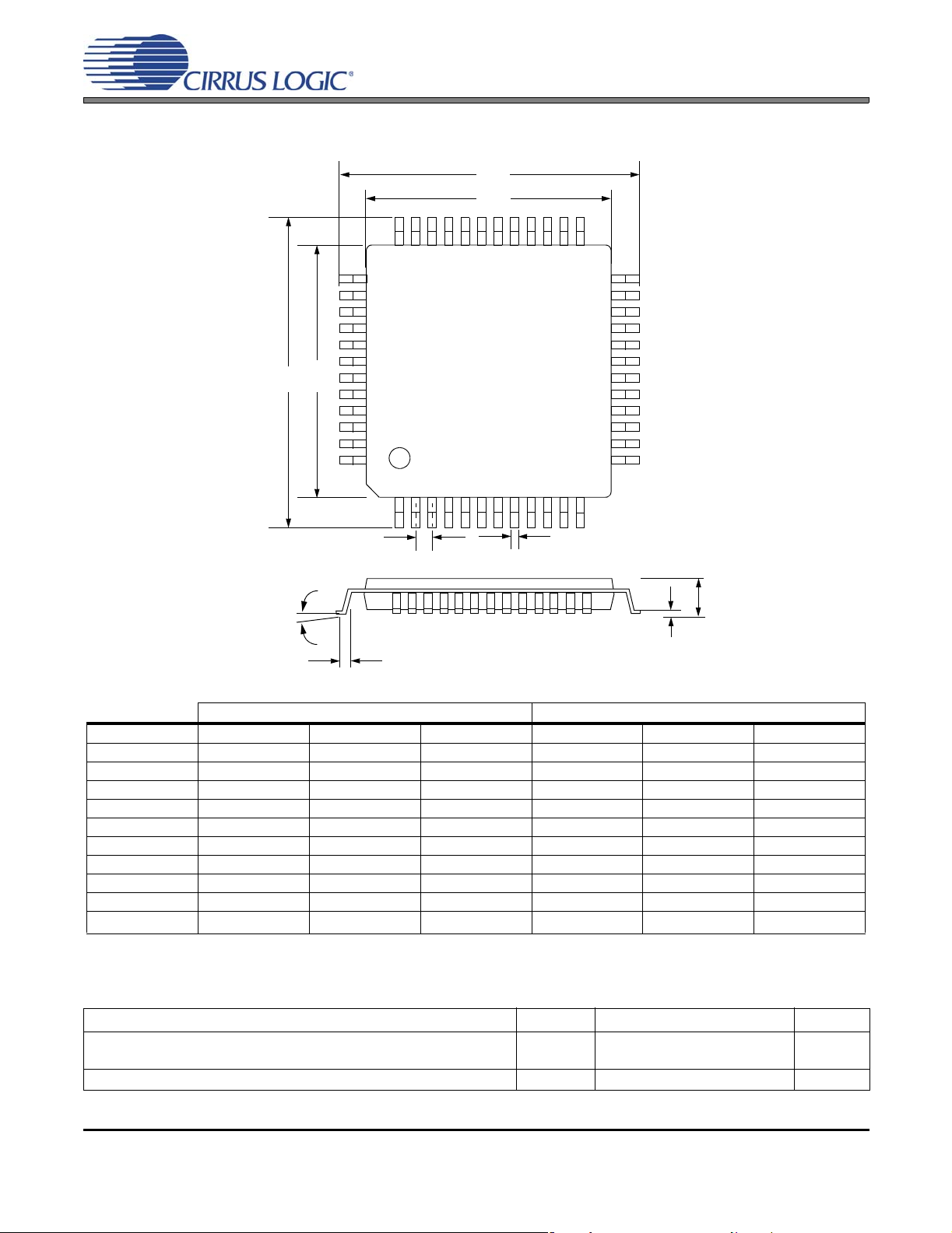
9. PACKAGE DIMENSIONS 48L LQFP PACKAGE DRAWING
D1
D
CS3318
E
E1
1
e
∝
B
A
A1
L
INCHES MILLIMETERS
DIM MIN NOM MAX MIN NOM MAX
A --- 0.055 0.063 --- 1.40 1.60
A1 0.002 0.004 0.006 0.05 0.10 0.15
B 0.007 0.009 0.011 0.17 0.22 0.27
D 0.343 0.354 0.366 8.70 9.0 BSC 9.30
D1 0.272 0.28 0.280 6.90 7.0 BSC 7.10
E 0.343 0.354 0.366 8.70 9.0 BSC 9.30
E1 0.272 0.28 0.280 6.90 7.0 BSC 7.10
e* 0.016 0.020 0.024 0.40 0.50 BSC 0.60
L 0.018 0.24 0.030 0.45 0.60 0.75
∝
* Nominal pin pitch is 0.50 mm *Controlling dimension is mm. *JEDEC Designation: MS022
0.000° 4° 7.000° 0.00° 4° 7.00°
10.THERMAL CHARACTERISTICS AND SPECIFICATIONS
Parameters Symbol Min Typ Max Units
Package Thermal Resistance (Note 1) 48-LQFP θ
Allowable Junction Temperature - - 125
1. θJA is specified according to JEDEC specifications for multi-layer PCBs.
DS693F1 43
JA
θ
JC
-
-
48
15
-
-
°C/Watt
°C/Watt
°C
Page 44

CS3318
11.ORDERING INFORMATION
Product Description Package Pb-Free Grade Temp Range Container Order #
CS3318
8-Channel
Analog Volume Control
48-pin
LQFP
YES Commercial -10° to +70° C
Tray CS3318-CQZ
Tape & Reel CS3318-CQZR
CDB3318 CS3318 Evaluation Board No - - - CDB3318
12.REVISION HISTORY
Release Changes
A1 Initial Rele ase of Advance Datasheet
PP1 Initial Release of Preliminary Datasheet
– Updated THD+N shown on cover page.
– Updated the RL measurement condition for the Analog Characteristics table on page 8.
– Updated THD+N specification in the Analog Characteristics table on page 8
– Updated Supply Current specifications in the Analog Characteristics table on page 8.
– Updated Power Consumption specification in the Analog Characteristics table on page 8.
– Updated Input/Output Voltage Range specification in the Analog Characteristics table on page 8.
– Updated Output Noise specification in the Analog Characteristics table on page 8.
– Updated Chip Revision bit description shown on page 41.
F1 Final Release
Contacting Cirrus Logic Support
For all product questions and inquiries, contact a Cirrus Logic Sales Representative.
To find the one nearest you, go to www.cirrus.com.
IMPORTANT NOTICE
Cirrus Logic, Inc. and its subsidiaries ("Cirrus") believe that the information contained in this document is accurate and reliable. However, the information is subject
to change without not ice and is pr ovided "AS IS" witho ut warr anty of any kind (express or implied). Customers are advised to obtain the latest version of relevant
information to verify, before placing orders, that information being relied on is current and complete. All products are sold subject to the terms and conditions of sale
supplied at the time of order acknowledgment, including those pertaining to warranty, indemnification, and limitation of liability. No responsibility is assumed by Cirrus
for the use of this information, including use of this information as the basis for manufacture or sale of any items, or for infringement of patents or other rights of third
parties. This document is the property of Cirrus and by furnishing this information, Cirrus grants no license, express or implied under any patents, mask work rights,
copyrights, trademarks, trade secrets or other inte llectual property rig hts. Cirrus owns the copyrights associated with the information contained herein and gives consent for copies to be made of the information only for use within your organization with respect to Cirrus integrated circuits or other products of Cirrus. This consent
does not extend to other copying such as copying for general distribution, advertising or promotional purposes, or for creating any work for resale.
CERTAIN APPLICATIONS USING SEMICONDUCTOR PRODUCTS MAY INVOLVE POTENTIAL RISKS OF DEATH, PERSONAL I NJURY, OR SEVERE PROPERTY OR ENVIRONMENTAL DAMAGE (“CRITICAL APPLICATIONS”). CIRRUS PRODUCTS ARE NOT DESIGNED, AUTHORIZED OR WARRANTED FOR USE
IN AIRCRAFT SYSTEMS, MILITARY APPLICATIONS, PRODUCTS SURGICALLY IMPLANTED INTO THE BODY, AUTOMOTIVE SAFETY OR SECURITY DEVICES, LIFE SUPPORT PRODUCTS OR OTHER CRITICAL APPLICATIONS. INCLUSION OF CIRRUS PRODUCTS IN SUCH APPLICATIONS IS UNDERSTOOD TO BE FULLY AT THE CUSTOMER’S RISK AND CIRRUS DISCLAIMS AND MAKES NO WARRANTY, EXPRESS, STATUTORY OR IMPLIED,
INCLUDING THE IMPLIED WARRANTIES OF MERCHANTABILITY AND FITNESS FOR PARTICULAR PURPOSE, WITH REGARD TO ANY CIRRUS PRODUCT
THAT IS USED IN SUCH A MANNER. IF THE CUSTOMER OR CUSTOMER’S CUSTOMER USES OR PERMITS THE USE OF CIRRUS PRODUCTS IN CRITICAL
APPLICATIONS, CUSTOMER AGREES, BY SUCH USE, T O FULLY INDEMNIF Y CIRRUS, ITS OF FICE RS, DI RECTORS, EMPLOYEES, DISTRI BUTORS AND
OTHER AGENTS FROM ANY AND ALL LIABILITY, INCLUDING ATTORNEYS’ FEES AND COSTS, THAT MAY RESULT FROM OR ARISE IN CONNECTION
WITH THESE USES.
Cirrus Logic, Cirrus, and the Cirrus Logic logo designs are trademarks of Cirrus Logic, Inc. All other brand and product names in this document may be trademarks
or service marks of their respective owners.
I²C is a registered trademark of Philips Semiconductor.
SPI is a trademark of Motorola, Inc.
44 DS693F1
 Loading...