

Page 1
Stereo Digital Volume Control
CS3310
Features
z Complete Digital Volume Control
— 2 Independent Channels
— Serial Control
— 0.5 dB Step Size
z Wide Adjustable Range
— -95.5 dB Attenuation
— +31.5 dB Gain
z Low Distortion & Noise
— 0.001% THD+N
— 116 dB Dynamic Range
z Noise Free Level Transitions
z Channel-to-Channel Crosstalk Better Than
110 dB
Description
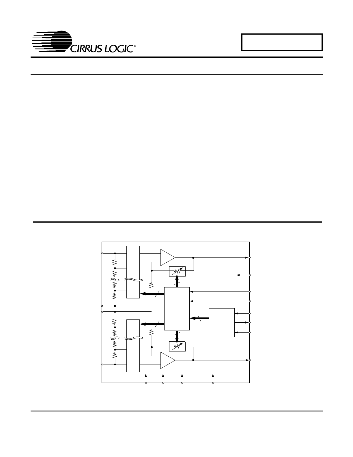
The CS3310 is a complete stereo digital volume control
designed specifically for audio systems. It features a 16bit serial interface that controls two independent, lowdistortion audio channels.
The CS3310 includes an array of well-matched resistors
and a low noise active output stage that is capable of
driving a 600 Ω load. A total adjustable range of 127 dB,
in 0.5 dB steps, is achieved through 95.5 dB of attenuation and 31.5 dB of gain.
The simple 3-wire interface provides daisy-chaining of
multiple CS3310's for multi-channel audio systems.
The device operates from ±5 V supplies and has an input/output voltage range of ±3.75 V.
ORDERING INFORMATION
CS3310-KS 0° to 70° C 16-pin Plastic SOIC
CS3310-KSZ, Lead Free 0° to 70° C 16-pin Plastic SOIC
Cirrus Logic, Inc.
www.cirrus.com
AINL
AGNDL
AGNDR
AINR
16
MUX
15
10
MUX
9
12
VA+
+
-
8
8
Control
Register
8
-
+
13
VA-
Copyright © Cirrus Logic, Inc. 2005
4
VD+
(All Rights Reserved)
16
Serial to
Parallel
Register
8
5
DGND
14
8
1
2
3
7
6
11
AOUTL
MUTE
ZCEN
CS
SDATAI
SDATAO
SCLK
AOUTR
SEPTEMBER '05
DS82F1
1
Page 2
CS3310
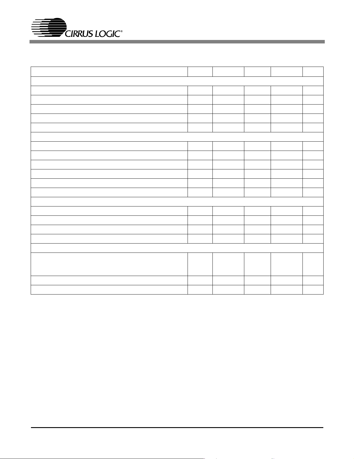
ANALOG CHARACTERISTICS (T
2kΩ; C
= 20 pF; 10 Hz to 20 kHz Measurement Bandwidth; unless otherwise specified)
L
= 25 °C, VA+, VD+ = 5 V ± 5%; VA- = -5V ± 5%; Rs = 0; RL =
A
Parameter Symbol Min Typ Max Unit
DC Characteristics
Step Size - 0.5 - dB
Gain Error (31.5 dB Gain) - ±0.05 - dB
Gain Matching Between Channels - ±0.05 - dB
Input Resistance R
Input Capacitance C
IN
IN
810-kΩ
-10-pF
AC Characteristics
Total Harmonic Distortion plus Noise (V in = 2V rms, 1 kHz) THD+N - 0.001 .0025 %
Dynamic Range 1 10 1 16 - dB
Input/Output Voltage Range (VA-)+1.25 - (VA+)-1.25 V
Output Noise (Note 1) - 4.2 8.4 µVrms
Digital Feedthrough (Peak Component) (Note 2) -80 - - dB
Interchannel Isolation (1 kHz) (Note 2) -100 -110 - dB
Output Buffer
Offset Voltage (Note 1) V
OS
- 0.25 0.75 mV
Load Capacitance - - 100 pF
Short Circuit Current - 20 - mA
Unity Gain Bandwidth, Small Signal (Note 2) 2 - - MHz
Power Supplies
Supply Current (No Load, AIN = 0 V) IA+
IA-
ID+
Power Consumption P
D
-
-
-
7.0
7.0
450
9.0
9.0
800
mA
mA
µA
-7294mW
Power Supply Rejection Ratio (250 Hz) PSRR - 80 - dB
Notes: 1. Measured with input grounded and Gain = 1. Will increase as a function of Gain settings >1.
2. This parameter is guaranteed by design and/or characterization.
2 DS82F1
Page 3
CS3310
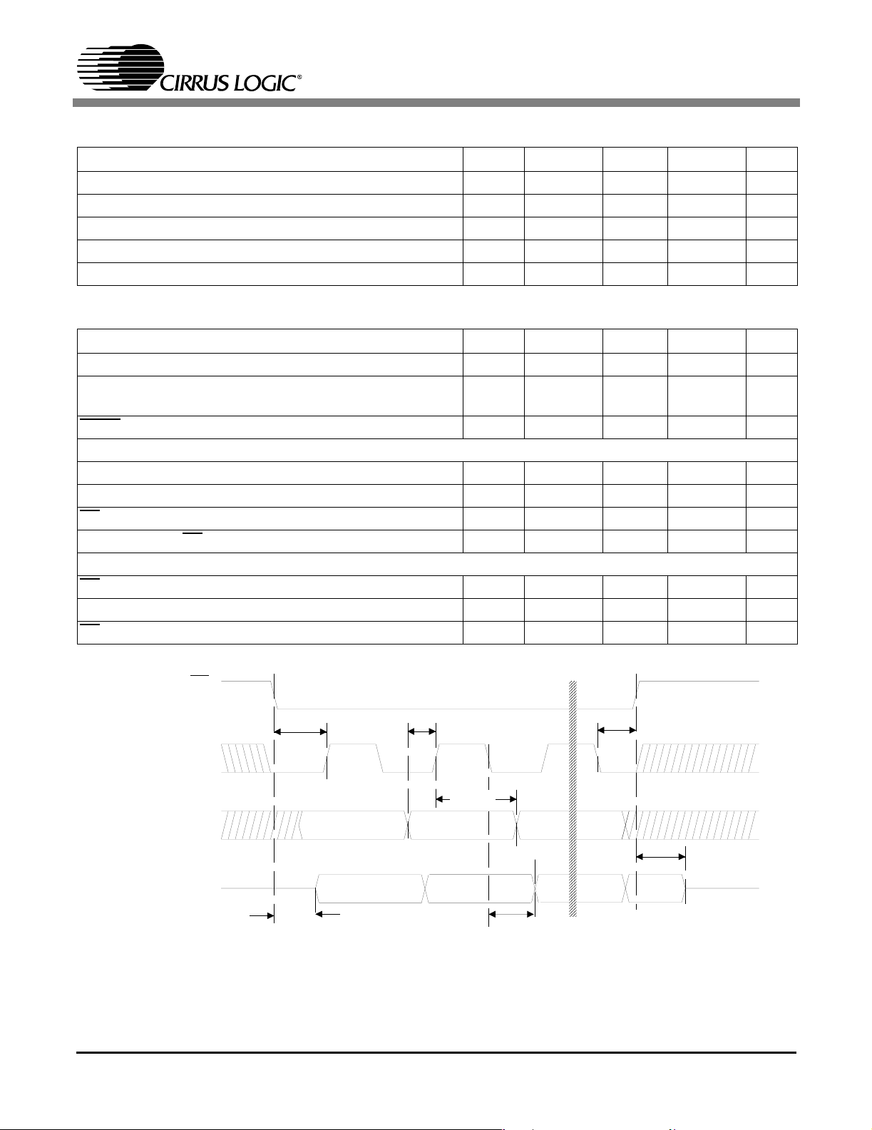
DIGITAL CHARACTERISTICS (T
= 25 °C, VA+ , VD+ = 5V ± 5%, VA- = -5V ± 5% )
A
Parameter Symbol Min Typ Max Unit
High-Level Input Voltage V
Low-Level Input Voltage V
High-Level Output Voltage (I
Low-Level Output Voltage (I
= 200µA) V
O
= 3.2mA) V
O
Input Leakage Current I
SWITCHING CHARACTERISTICS
(TA = 25 °C; VA+, VD+ = +5V ± 5%; VA- = -5V ± 5%; CL = 20 pF)
IH
IL
OH
OL
in
2.0 - VD+0.3 V
-0.3 - +0.8 V
VD-1.0 - - V
--0.4V
-1.010µA
Parameter Symbol Min Typ Max Unit
Serial Clock SCLK 0 - - MHz
Serial Clock Pulse Width High
Pulse Width Low
MUTE
Pulse Width Low - 2.0 - - ms
t
ph
t
pl
80
80
-
-
-
-
ns
ns
Input Timing
SDATAI Set Up Time t
SDATAI Hold Time t
CS
Valid to SCLK Rising t
SCLK Falling to CS
High t
SDVS
SDH
CSVS
LTH
20 - - ns
20 - - ns
30 - - ns
35 - - ns
Output Timing
CS
Low to Output Active t
SCLK Falling to Data Valid t
CS
High to SDATAO Inactive t
CSH
SSD
CSDH
- - 35 ns
- - 60 ns
--100ns
CS
SCLK
SDATAI
SDATAO
t
CSVS
t
MSB
CSH
t
SDVS
t
SDH
t
SSD
t
LTH
t
CSDH
Figure 1. Serial Port Timing Diagram
DS82F1 3
Page 4
CS3310
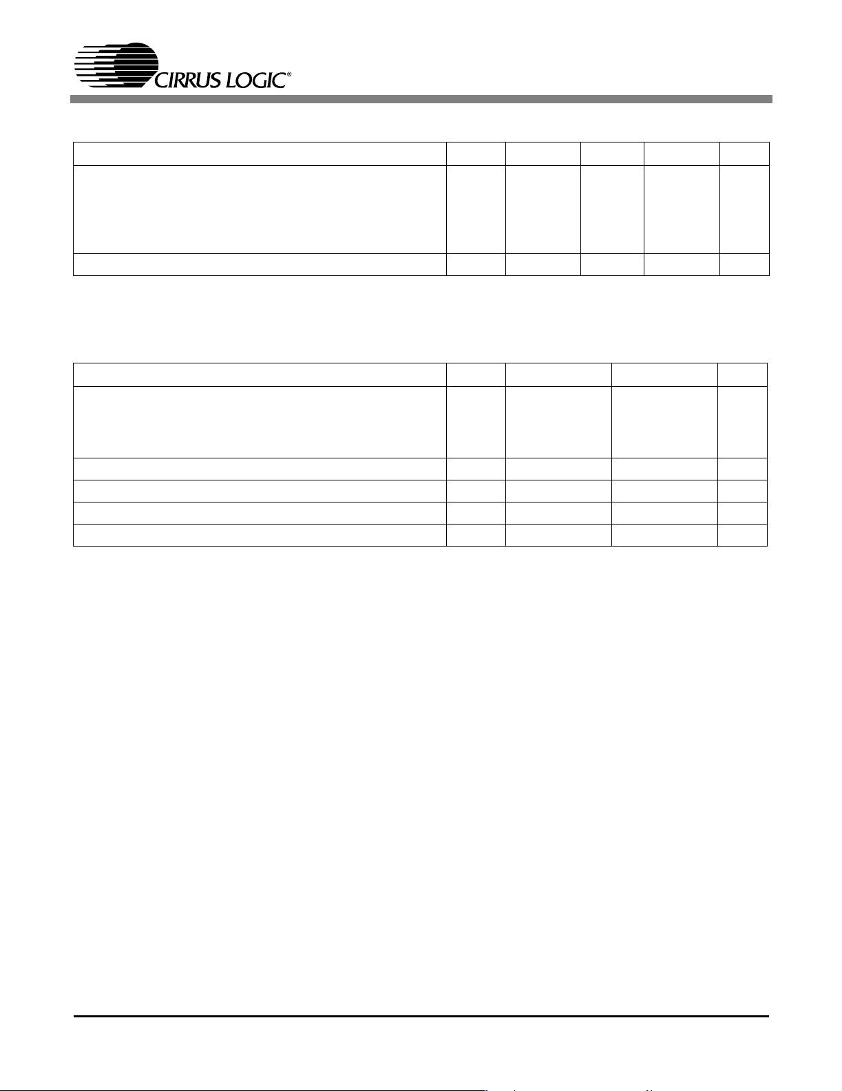
RECOMMENDED OPERATING CONDITIONS
Parameter Symbol Min Typ Max Unit
DC Power Supplies:
Positive Digital
Positive Analog
Negative Analog
(VD+) - (VA+) (Note 3)
Ambient Operating Temperature T
Notes: 3. Applying power to VD+ prior to VA+ creates a SCR latch-up condition. Refer to Figure 2 for the
recommended power connections.
(DGND = 0V; all voltages with respect to ground)
VD+
VA+
VA
-
A
4.75
4.75
-4.75
-0.3
02570°C
5.0
5.0
-5.0
-
VA+
5.25
-5.25
0.0
ABSOLUTE MAXIMUM RATINGS (AGND, DGND = 0V, all voltages with respect to ground.)
Parameter Symbol Min Max Unit
DC Power Supplies:
Positive Digital
Positive Analog
Negative Analog
Input Current, Any Pin Except Supply I
Digital Input Voltage V
Ambient Operating Temperature (power applied) T
Storage Temperature T
VD+
VA+
VA-
in
IND
A
STG
-0.3
-0.3
0.3
- ±10 mA
-0.3 (VA+) + 0.3 V
-55 +125 °C
-65 +150 °C
(VA+)+ 0.3
6.0
-6.0
V
V
V
V
V
V
V
4 DS82F1
Page 5
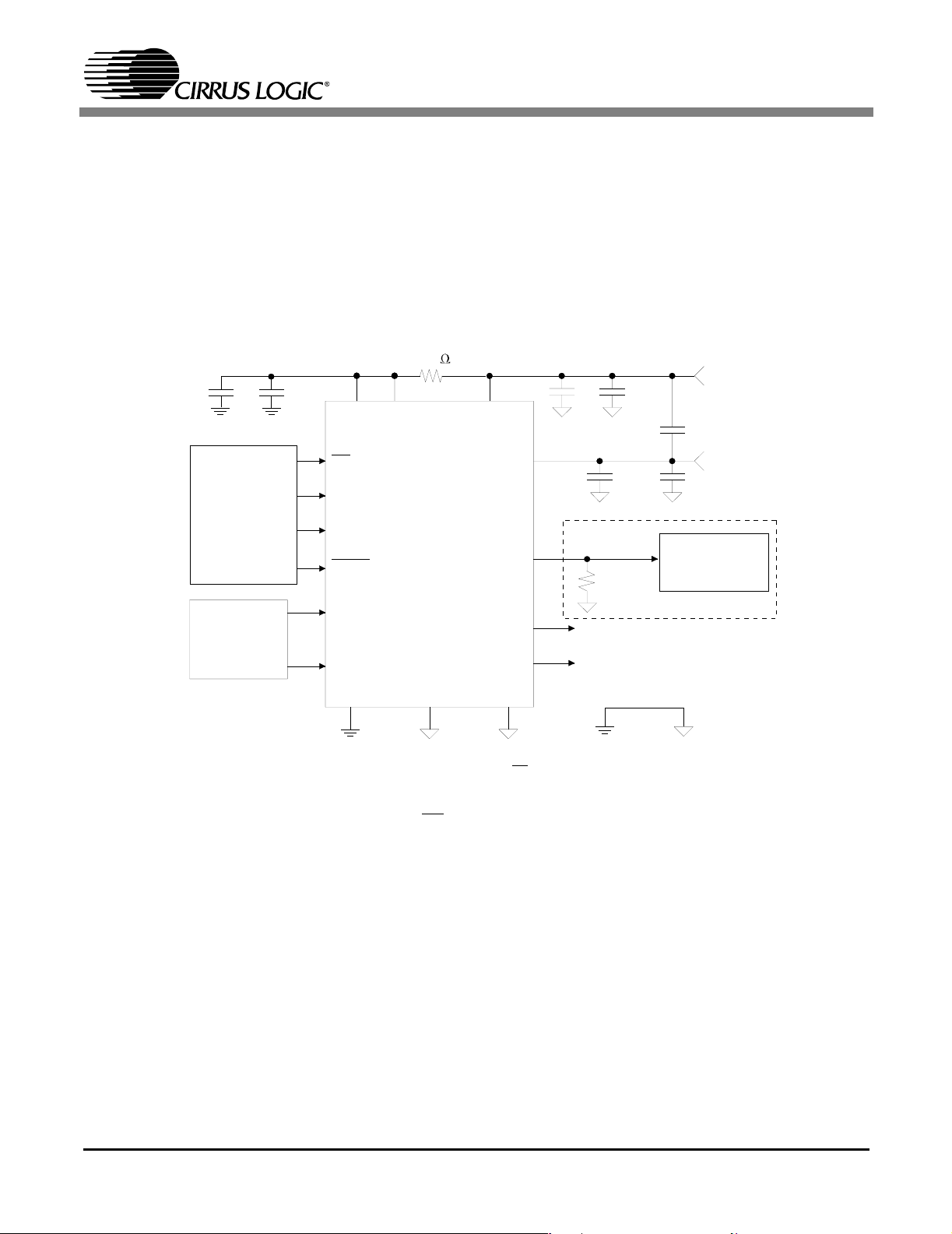
+
10
µ
F
CONTROLLER
AUDIO
SOURCE
0.1 µF
2
3
6
8
16
9
1
ZCEN
CS
SDATAI
SCLK
MUTE
AINL
AINR
DGND
5
**
10
4
VD+ VA+
CS3310
AGNDL AGNDR
12
SDATAO
AOUTL
AOUTR
15
0.1 µF
VA-
10
13
7
14
11
0.1 µF
*
+
47 k
AUDIO
OUTPUTS
10
10 µF
Ω
µ
F
0.1 µF
+
TO ANOTHER
CS3310 OR
CONTROLLER
CS3310
+5V ANALOG
-5V ANALOG
*Required to terminate SDATAI due to high impedance
state of SDATAO when CS
is high.
**Refer to Note 3.
Figure 2. Recommended Connection Diagram
DS82F1 5
Page 6
CS3310
GENERAL DESCRIPTION
The CS3310 is a stereo, digital volume control designed for audio systems. The levels of the left
and right analog input channels are set by a 16-bit serial data word; the first 8 bits address the
right channel and the remaining 8 bits address the left channel, as detailed in Table 1. Resistor
values are decoded to 0.5 dB resolution by an internal multiplexer for a total attenuation range of
-95.5 dB. An output amplifier stage provides a programmable gain of up to 31.5 dB in 0.5 dB
steps. This results in an overall 8-bit adjustable range of 127 dB.
The CS3310 operates from ±5 V supplies and accepts inputs up to ±3.75 V. Once in operation,
the CS3310 can be brought to a muted state with the mute pin, MUTE, or by writing all zeros to
the volume control registers. The device contains a simple three wire serial interface which accepts 16-bit data. This interface also supports daisy-chaining capability.
SYSTEM DESIGN
Very few external components are required to support the CS3310. Normal power supply decoupling components are all that is required, as shown in Figure 2.
Serial Data Interface
The CS3310 has a simple, three wire interface that consists of three input pins: SDATAI, serial
data input; SCLK, serial data clock and CS, the chip select input. SDATAO, serial data output,
enables the user to read the current volume setting or provide daisy-chaining of multiple
CS3310’s.
The 16-bit serial data is formatted MSB first and clocked into SDATAI by the rising edge of SCLK
with CS
output levels of both left and right channels are set. The existing data in the volume control data
register is clocked out SDATAO on the falling edge of SCLK. This data can be used to read current gain/attenuation levels or to daisy chain multiple CS3310’s. See Figure 1 for proper setup
and hold times for CS, SDATAI, SCLK, and SDATAO. SCLK and SDATAI should be active only
during volume setting operations to achieve optimum dynamic range.
low as shown in Figure 3. The data is latched by the rising edge of CS and the analog
Daisy Chaining
Digitally controlled, multi-channel audio systems often result in complex address decoding which
complicates PCB layout. This is greatly simplified with the daisy-chaining capability of the
CS3310.
6 DS82F1
Page 7

CS
SCLK
CS3310
SDATAI
SDATAO
R7 R6 R5 R4 R3 R2 R1 R0 L7 L6 L5 L4 L3 L2 L1 L0
R7 R6 R5 R4 R3 R2 R1 R0 L7 L6 L5 L4 L3 L2 L1 L0
L0 = Left Channel Least Signif icant B it R0 = Right Channel Least Significant Bi t
L7 = Left Channel Most Si gnific ant B it R7 = Right Channel Most Signifi cant B i t
SDATAI is latched internally on the rising edge of SCLK
SDATAO transi t ions after t he falli ng edge of SC LK
SDATAO bi ts reflect the data previously loaded into t he C S3310
Figure 3. Serial Port Timing
In single device operation, volume control data is loaded into the 16-bit shift register by holding
the CS pin low for sixteen SCLK pulses and then latched on the rising edge of CS. The previous
contents of the shift-register are shifted through the register and out SDATAO during the process.
Multi-channel operation can be implemented as shown in Figure 4 by connecting the SDATAO
of device #1 to the SDATAI pin of device #2. In this manner multiple CS3310s can be loaded from
a single serial data line without complex addressing schemes. Volume control data is loaded by
holding CS low for 16 x N SCLK pulses, where N is the number of devices in the chain. The 16
bits clocked into device #1 on SCLK pulses 1-16 are clocked into device #2 on SCLK pulses 17-
32. The CS3310s are simultaneously updated on the rising edge of CS following 16 x N SCLK
pulses Notice that a 47 kohm resistor is required to terminate SDATAI, as shown in Figure 4, due
to the high impedance state of SDATAO when CS is high..
AUDIO
SIGNAL
AUDIO
SIGNAL
16
9
47 k
16
9
SDATAI
AINL
AINR
SDATAO
SDATAI
AINL
AINR
SDATAO
3
CS3310
7
3
CS3310
7
#1
#2
SCLK
CS
AOUTL
AOUTR
SCLK
CS
AOUTL
AOUTR
6
2
14
11
6
2
14
11
CONTROLLER
Figure 4. Daisy Chaining Diagram
DS82F1 7
Page 8

CS3310
Changing the Analog Output Level
Care has been taken to ensure that there are no audible artifacts in the analog output signal during volume control changes. The gain/attenuation changes of the CS3310 occur at zero crossings to eliminate glitches during level transitions. The zero crossing for the left channel is the
voltage potential at the AGNDL pin; the voltage potential at the AGNDR pin defines the right
channel zero crossing.
A volume control change occurs after chip select latches the data in the volume control data register and two zero crossings are detected. If two zero crossings are not detected within 18 ms of
the change in CS, the new volume setting is implemented. The zero crossing enable pin, ZCEN,
enables or disables the zero crossing detection function as well as the 18 ms time-out circuit.
Input Code
(Left or Right Channel) Gain or Attenuation (dB)
11111111
11111110
•
•
11000000
•
00000010
00000001
00000000
Table 1. Input Code Definition
+31.5
+31.0
•
•
0
•
-95.0
-95.5
Software Mute
Analog Inputs and Outputs
The maximum input level is limited by the common-mode voltage capabilities of the internal opamp. Signals approaching the analog supply voltages may be applied to the AIN pins if the internal attenuator limits the output signal to within 1.25 volts of the analog supply rails.
The outputs are capable of driving 600 Ω loads to within 1.25 volts of the analog supply rails and
are short circuit protected to 20 mA.
As with any adjustable gain stage the affects of a DC offset at the input must be considered. Capacitively coupling the analog inputs may be required to prevent “clicks and pops” which occur
with gain changes if an appreciable offset is present.
Source Impedance Requirements
The CS3310 requires a low source impedance to achieve maximum performance. The ESD protection diodes on the analog input pins are reversed biased during normal operation. A characteristic of a reversed biased diode is a non-linear voltage dependent capacitance which can be
8 DS82F1
Page 9

CS3310
a source of distortion if the source impedance becomes appreciable relative to the reversed biased diode capacitance. Source impedances equal to or less than 600 ohms will avoid this distortion mechanism for the CS3310.
Mute
Muting can be achieved by either hardware or software control. Hardware muting is accomplished via the MUTE input and software muting by loading all zeroes into the volume control register.
MUTE disconnects the internal buffer amplifiers from the output pins and terminates AOUTL and
AOUTR with 10 kΩ resistors to ground. The mute is activated with a zero crossing detection (independent of the zero cross enable status) or an 18 ms timeout to eliminate any audible “clicks”
or “pops”. MUTE also initiates an internal offset calibration.
A software mute is implemented by loading all zeroes into the volume control register. The internal amplifier is set to unity gain with the amplifier input connected to the maximum attenuation
point of the resistive divider, AGND.
A “soft mute” can be accomplished by sequentially ramping down from the current volume control
setting to the maximum attenuation code of all zeroes.
Power-Up Considerations
Upon initial application of power, the MUTE pin of the CS3310 should be set low to initiate a power-up sequence. This sequence sets the serial shift register and the volume control register to
zero and performs an offset calibration. The device should remain muted until the supply voltages have settled to ensure an accurate calibration. The device also includes an internal power-on
reset circuit that requires approximately 100 µs to settle and will ignore any attempts to address
the internal registers during this period.
The offset calibration minimizes internally generated offsets and ignores offsets applied to the
AIN pins. External clocks are not required for calibration.
Although the device is tolerant to power supply variation, the device will enter a hardware mute
state if the power supply voltage drops below approximately ±3.5 volts. A power-up sequence
will be initiated if the power supply voltage returns to greater than ±3.5 volts.
Applying power to VD+ prior to VA+ creates a SCR latch-up condition. Refer to Figure 2 for the
recommended power connections.
DS82F1 9
Page 10

CS3310
PCB Layout, Grounding and Power Supply Decoupling
As with any high performance device which contains both analog and digital circuitry, careful attention to power supply and grounding arrangements must be observed to optimize performance.
Figure 2 shows the recommended power arrangements with VA+ connected to a clean +5 volt
supply and VA- connected to a clean -5 volt supply. VD+ powers the digital interface circuitry and
should be powered from VA+, as shown in Figure 2, to avoid potentially destructive SCR latchup. Decoupling capacitors should be located as near to the CS3310 as possible, see Figure 5.
Figure 5. Recommended 2-Layer PCB Layout
Analog Ground Plane
Ω
10 µF
0.1
10
+
µ
F
10 µF
0.1
+
VA+
VA-
10 µF
+
0.1 µF
F
µ
The printed circuit board layout should have separate analog and digital regions with individual
ground planes. The CS3310 should reside in the analog region as shown in Figure 5. Care
should be taken to ensure that there is minimal resistance in the analog ground leads to the device to prevent any change in the defined attenuation settings. Extensive use of ground plane fill
on both the analog and digital sections of the circuit board will yield large reductions in radiated
noise effects.
Performance Plots
Figure 8 displays the CS3310 frequency response with a 3.75 Vp output.
Figure 9 shows the frequency response with a 0.375 Vp output.
Figure 6 is the Total Harmonic Distortion + Noise vs. amplitude at 1 kHz. The upper trace is the
THD+N vs. amplitude of the CS3310 The lower trace is the THD+N of the Audio Precision System One generator output connected directly to the analyzer input. The System One panel settings are identical to the previous test. This indicates that the THD+N contribution of the Audio
Precision actually degrades the measured performance of the CS3310 below 2.7 Vrms signal
levels.
10 DS82F1
Page 11

CS3310
Figure 7 is a 16k FFT plot demonstrating the crosstalk performance of the CS3310 at 20 kHz.
Both channels were set to unity gain. The right channel input is grounded with the left channel
driven to 2.65 Vrms output at 20 kHz. The FFT plot is of the right channel output. This indicates
channel to channel crosstalk of -130 dB at 20 kHz.
Figure 10 is a series of plots which display the unity-gain THD+N vs. Frequency for 600 Ω, 2 kΩ
and infinite load conditions. The output was set to 2 Vrms. The Audio Precision System One was
bandlimited to 22 kHz
Figure 11 is a series of plots which display the unity-gain THD+N vs. Frequency for 1, 2 and 2.8
Vrms output levels. The output load was open circuit. The Audio Precision System One was
bandlimited to 22 kHz.
DS82F1 11
Page 12

CS3310
.
1
.1
.01
.001
.0001
0.1 1
THD+N% vs AMPL (Vrms)
Figure 6. THD+N vs. AMP Figure 7. 20 kHz Crosstalk
1.0
0.5
0.0
-0.5
AMPL (d Br) vs FREQ ( Hz)
0
-20
-40
-60
-80
-100
-120
-140
-160
3
-180
-0.5
1.0
0.5
0.0
20.00
2.06k
AMPL (dBr) vs FREQ (Hz)
4.11k 6.15k 8.19k
AMPL (d Br) vs FREQ ( Hz)
10.2k
12.3k
14.3k 16.4k 18.4k
20.5k
22.5k
-1.0
-1.5
-2.0
10
100
1k
10k
100k
200k
-1.0
-1.5
-2.0
10
100
1k
10k
100k
Figure 8. Frequency Response Full Scale Input Figure 9. Frequency Response -20 dB Input
0.1000
600
2k
OPEN
Ω
Ω
0.0100
0.0010
0.0001
20 100 1k 10k 20k
Figure 10. THD+N vs. Frequency LOAD = 600 Ω,
2kΩ, open ckt
0.1000
0.0100
0.0010
0.0001
20 100 1k 10k 20k
2.8 VRMS
2 VRMS
1 VRMS
Figure 11. THD+N vs. Frequency Output levels of
1, 2, and 2.8 Vrms
200k
12 DS82F1
Page 13

PIN DESCRIPTION
CS3310
Zero Crossing Enable ZCEN AINL Left Channel Input
Chip Select CS
Serial Data Input SDATAI AOUTL Left Channel Output
Positive Digital Power VD+ VA- Negative Analog Power
Digital Ground DGND VA+ Positive Analog Power
Serial Clock Input SCLK AOUTR Right Channel Output
Serial Data Output SDATAO AGNDR Right Analog Ground
Mute MUTE
Power Supply Connections
VA+ - Positive Analog Power, Pin 12.
Positive analog supply. Nominally +5 volts.
VA- - Negative Analog Power, Pin 13.
1
2
3
4
5
6
7
8
16
15
AGNDL Left Analog Ground
14
13
12
11
10
AINR Right Channel Input
9
Negative analog supply. Nominally -5 volts.
AGNDL - Left Channel Analog Ground, Pin 15.
Analog ground reference for the left channel.
AGNDR - Right Channel Analog Ground, Pin 10.
Analog ground reference for the right channel.
VD+ - Positive Digital Power, Pin 4.
Positive supply for the digital section. Nominally +5 volts. Applying power to VD+ prior
to VA+ creates a SCR latch-up condition. Refer to Figure 2 for the recommended
power connections.
DGND - Digital Ground, Pin 5.
Digital ground for the digital section.
DS82F1 13
Page 14

Analog Inputs and Outputs
AINL, AINR - Left and Right Channel Analog Inputs, Pins 16, 9.
Analog input connections for the left and right channels. Nominally ±3.75 volts for a full
scale input.
AOUTL, AOUTR - Left and Right Channel Analog Outputs, Pins 14, 11.
Analog outputs for the left and right channels. Nominally ±3.75 volts for a full scale
output.
Digital Pins
SDATAI - Serial Data Input, Pin 3.
Serial input data that sets the analog output level of the left and right channels. The
data is formatted in a 16-bit word. The first eight bits clocked into this pin control the
analog output level for the right channel, and the second eight bits clocked into the
device control the analog output level for the left channel. The data is clocked into the
CS3310 by the rising edge of SCLK.
CS3310
SDATAO - Serial Data Output, Pin 7.
Serial output data that provides daisy-chaining of multiple CS3310’s. This serial output
will output the previous sixteen bits of volume control data that were clocked into the
SDATAI pin. SDATAO will enter a High Impedance State when CS is High.
SCLK - Serial Input Clock, Pin 6.
Serial clock that clocks in the individual bits of serial data from the SDATAI pin. This
clock is also used to clock out the individual bits from the SDATAO pin. The SDATAI
data is latched on the rising edge, and SDATAO data is clocked out on the falling
edge.
- Chip Select, Pin 2.
CS
When high, the SDATAO output is held in a high impedance state. A falling transition
defines the start of the 16-bit volume control word into the device. The 16-bit input
data is latched into the control register on the rising edge of CS
MUTE
- Mute, Pin 8.
Forces both the left and right analog output channels to ground. An offset calibration is
initiated following the low transition of MUTE. Calibration requires a minimum mute
period of 2 ms.
.
14 DS82F1
Page 15

ZCEN - Zero Crossing Enable, Pin 1.
This pin enables or disables the zero crossing detection and time-out function used
during analog output level transitions. A high level on this pin enables the zero
crossing detection function. A low level on this pin disables the zero crossing
detection.
PARAMETER DEFINITIONS
CS3310
Dynamic Range
Full scale (RMS) signal to broadband noise ratio. The broadband noise is measured
over the specified bandwidth with the input grounded. Units in decibels.
Total Harmonic Distortion plus Noise
The ratio of the rms value of the signal to the rms sum of all other spectral
components over the specified bandwidth (typically 10 Hz to 20 kHz), including
distortion components. Expressed in decibels.
Interchannel Isolation
A measure of crosstalk between the left and right channels. Measured for each
channel at the converter’s output with the input under test grounded and a full-scale
signal applied to the other channel. Units in decibels.
DS82F1 15
Page 16

PACKAGE DIMENSIONS
16L SOIC (300 MIL BODY) PACKAGE DRAWING
1
b
CS3310
E
H
SEATING
PLANE
D
A
e
A1
c
L
INCHES MILLIMETERS
DIM MIN MAX MIN MAX
A 0.093 0.104 2.35 2.65
A1 0.004 0.012 0.10 0.30
B 0.013 0.020 0.33 0.51
C 0.009 0.013 0 .23 0.32
D 0.398 0.413 10.10 10.50
E 0.291 0.299 7.40 7.60
e 0.040 0.060 1.02 1.52
H 0.394 0.419 10.00 10.65
L 0.016 0.050 0.40 1.27
∝ 0° 8° 0° 8°
JEDEC #: MS-013
∝
16 DS82F1
Page 17

Revision Date Changes
PP1 April 1991 Initial release
PP2 December 1992 Update specifications
PP3 February 1999 Update specifications
PP4
July 2004
F1 September 2005 Added “Lead Free” to Ordering Information on front page.
Update specifications and bring into new template.
Add lead free part.
CS3310
Contacting Cirrus Logic Support
For all product questions and inquiries contact a Cirrus Logic Sales Representative.
To find one nearest you go to www.cirrus.com
IIMPORTANT NOTICE
Cirrus Logic, Inc. and its subsidiaries ("Cirrus") believe that the information contained in this document is ac curate and reliable. However, the information is subject
to change without notice and is pr ovided " AS IS" withou t warrant y of any ki nd (expr ess or impl ied). Cust omers ar e advised t o obtain the latest version of relevant
information to verify, before placing ord ers, tha t inform ation bein g rel ied on is curr ent an d com ple te. All p roducts a re sol d su bject to the te rms and co nd itions o f sale
supplied at the time of order acknowledgment, including those pertaining to warranty, indemnification, and limitation of liability. No responsibility is assumed by Cirrus
for the use of this information, including use of this information as the basis for manufacture or sale of any items, or for infringement of patents or other rights of third
parties. This document is the property of Cirrus and by furnishi ng this informa tion, Cirru s gran ts no lice nse, expr ess or impl ied under an y patents, mask wo rk rights,
copyrights, trademarks, trade secrets or other intellectual property rights. Cirrus owns the copyrights associated with the information contained herein and gives con sent for copies to be made of the information only for use within your organization with respect to Cirrus integrated circuits or other products of Cirrus. This consent
does not extend to other copying such as copying for general distribution, advertising or promotional purposes, or for creatin g an y work for resale.
CERTAIN APPLICATIONS USING SEMICONDUCTOR PRODUCTS MAY INVOLVE POTENTIAL RISKS OF DEATH, PERSONAL INJURY, OR SEVERE PROPERTY OR ENVIRONMENTAL DAMAGE (“CRITICAL APPLICATIONS”). CIRRUS PRODUCTS ARE NOT DESIGNED, AUTHORIZED OR WARRANTED FOR USE
IN AIRCRAFT SYSTEMS, MILI TARY A PPLICAT IONS, PRODUCTS SURG ICALLY IMPLANTE D INT O THE BODY, AUTOMOTIV E SAFETY OR SECURI TY DEVICES, LIFE SUPPORT PRODUCTS OR OTHER CRITICAL APPLICATIONS. INCLUSION OF CIRRUS PRODUCTS IN SUCH APPLICATIONS IS UNDERSTOOD TO BE FULLY AT THE CUSTOMER’S RISK AND CIRRUS DISCLAIMS AND MAKES NO WARRANTY, EXPRESS, STATUTORY OR IMPLIED,
INCLUDING THE IMPLIED WARRANTIES OF MERCHANTABILITY AND FITNESS FOR PARTICULAR PURPOSE, WITH REGARD TO ANY CIRRUS PRODUCT
THAT IS USED IN SUCH A MANNER. IF THE CUSTOMER OR CUSTOMER’S CUSTOMER U SES OR PERMITS THE USE OF CIRRUS PRODUCTS IN CRITICAL
APPLICATIONS, CUSTOMER AGREES, BY SUCH USE, TO FULL Y INDEMNI FY CI RRUS, I TS OFFI CERS , DI RECT ORS, EMPLOYEE S, DISTRI BUTORS A ND
OTHER AGENTS FROM ANY AND ALL LIABILITY , INCLUDING AT TORNEYS’ FEES AND COSTS, THAT MAY RESULT FROM OR ARISE IN CONNECTION
WITH THESE USES.
Cirrus Logic, Cirrus, and the Cirrus Logic logo designs are trademarks of Cirrus Logic, Inc. All other brand and product names in this document may be trademarks
or service marks of their respective owners.
DS82F1 17
 Loading...