

CS3301A
Low-noise, Programmable Gain, Differential Amplifier
Features & Desription
z Signal Bandwidth: DC to 2 kHz
z Selectable Gain: x1, x2, x4, x8, x16, x32, x64
z Differential Inputs, Differential Outputs
• Multiplexed inputs: INA, INB, 800Ω termination
• Rough / fine outputs for CS5371A / 72A / 73A
• Max signal amplitude: 5 V
• Low input bias: 1 nA typical
Outstanding Noise Performance
z
nV/ Hz
• 8.5 from 0.1 Hz to 2 kHz
•0.180µV
Low Total Harmonic Distortion
z
• -121 dB THD typical (0.0000891%)
• -112 dB THD maximum (0.0002512%)
Low Power Consumption
z
• Normal operation: 5.5 mA typical
• Power down: 10 µA typical
Small 24-pin SSOP Package
z
z Bipolar Power Supply Configuration
• VA+ = +2.5 V; VA- = -2.5 V; VD = +3.3 V
between 0.1 Hz and 10 Hz
p-p
differential
pp
Description
The CS3301A is a low-noise differential input, differential output amplifier with programmable gain,
optimized for amplifying signals from low-impedance sensors such as geophones. The gain
settings are binary weighted (x1, x2, x4, x8, x16,
x32, x64) and are selected using simple pin settings. Two sets of external inputs, INA and INB,
simplify system design as inputs from a sensor and
test DAC. An internal 800 Ω termination can also be
selected for noise tests.
Amplifier noise performance is outstanding with a
noise density of 8.5 over the 0.1 Hz to
2 kHz bandwidth. Distortion performance is also extremely good, typically -121 dB THD at x1 gain. Flat
noise down to 0.1 Hz and low total harmonic distortion make this amplifier ideal for low-frequency,
low-amplitude, differential signals requiring maximum dynamic range.
ORDERING INFORMATION
See page 15.
nV/ Hz
http://www.cirrus.com
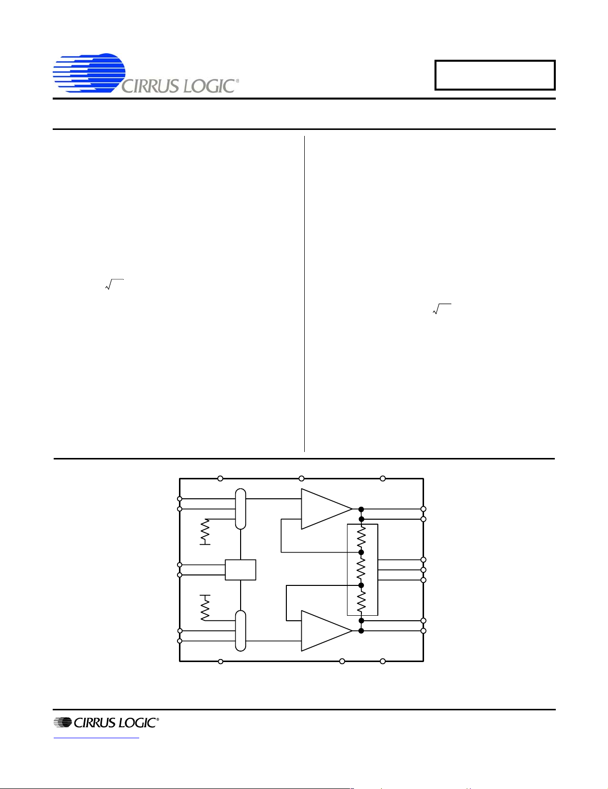
INA+
INB+
MUX0
MUX1
INAINB-
VA+
400 Ω 400 Ω
VA-
Copyright © Cirrus Logic, Inc. 2007
CLK
+
-
-
+
PWDN
(All Rights Reserved)
VD
OUTR+
OUTF+
GAIN0
GAIN1
GAIN2
OUTFOUTR-
GND
MAR ‘07
DS757F1

TABLE OF CONTENTS
1. CHARACTERISTICS AND SPECIFICATIONS .............................................................................. 3
SPECIFIED OPERATING CONDITIONS ....................................................................................... 3
ABSOLUTE MAXIMUM RATINGS ................................................................................................. 3
TEMPERATURE CONDITIONS ........ .... ... ... ... ... .... ... .......................................... ... ... .... ... ..............3
ANALOG CHARACTERISTICS ..................................................................................................... 4
DIGITAL CHARACTERISTICS ......................................................................................................7
POWER SUPPLY CHARACTER ISTICS ................... ....................... ................... ................... ........ 8
2. GENERAL DESCRIPTION ............................................................................................................. 9
2.1.Analog Signals................. .... .......................................... ... ... ... ..................................................9
2.2.1. Analog Inputs................................................................................................................9
2.3.2. Analog Outputs.............................................................................................................9
2.4.3. Differential Signals............ .... ... ... ... ... .... .......................................... ... ... ... .... ... ... ... ... ...10
2.5.Digital Signals.........................................................................................................................10
2.6.1. Clock Input..................................................................................................................10
2.7.2. Gain Selection ............................................................................................................10
2.8.3. Mux Selection .............................................................................................................10
2.9.4. Power Down Selection...... .... ... ... ... ... .... ... ................................................................... 11
2.10.Power Supplies .............. .... ... ... ... .... ... ... .......................................... ... ... .... ... .........................11
2.11.1. Analog Power Supplies...............................................................................................11
2.12.2. Digital Power Supplies................................................................................................11
2.13.Connection Diagram..............................................................................................................12
3. PIN DESCRIPTION.......................................................................................................................13
4. PACKAGE DIMENSIONS...... .... ... ... .......................................... ... .... ... ... ... ... .... ... .........................14
5. ORDERING INFORMATION ........................................................................................................ 15
6. ENVIRONMENTAL, MANUFACTURING, & HANDLING INFORMATION .................................. 15
7. REVISION HISTORY ................................................... ... .... ... .......................................... ... ......... 16
CS3301A
LIST OF FIGURES
Figure 1. CS3301A Noise Performance..........................................................................................4
Figure 2. Digital Input Rise and Fall Times .....................................................................................7
Figure 3. Multi-Channel System Architecture.................................................................................. 9
Figure 4. Single-Channel System Architecture ............................................................................. 10
Figure 5. CS3301A Amplifier Connections....................................................................................12
Figure 6. CS3301A Pin Assignments............................................................................................13
LIST OF TABLES
Table 1. Digital Selections for Gain and Input Mux Control . ...........................................................7
Table 2. Pin Descriptions .............................................................................................................13
2 DS757F1
CS3301A
1. CHARACTERISTICS AND SPECIFICATIONS
• Min / Max characteristics and specifications are guaranteed over the Specified Operating Conditions.
• Typical performance characteristics and specifications are measured at nominal supply voltages and T
• GND = 0 V. Single-ended voltages with respect to GND, differential voltages with respect to opposite half.
• Device is connected as shown in Figure 5 on page 12 unless otherwise noted.
SPECIFIED OPERATING CONDITIONS
Parameter Symbol Min Nom Max Unit
Bipolar Power Supplies
Positive Analog ± 2 % VA+ 2.45 2.50 2.55 V
Negative Analog (Note 1) ± 2% V A- -2.55 -2.50 -2.45 V
Positive Digital (Note 2) ± 3% VD 3.20 3.30 3.40 V
Thermal
Ambient Operating Temperature Industrial (-IS, -ISZ) T
A
Notes: 1. VA- must be the most negative voltage to avoid potential SCR latch-up conditions.
2. VD must conform to Digital Supply Differential under Absolute Maximum Ratings.
-40 25 85 °C
= 25°C.
A
ABSOLUTE MAXIMUM RATINGS
Parameter Symbol Min Max Parameter
DC Power Supplies Positive Analog
Negative Analog
Digital
Analog Supply Differential [(VA+) - (VA-)] VA
Digital Supply Differential [(VD) - (VA-)] VD
Input Current, Power Supplies (Note 3)I
Input Current, Any Pin Except Supplies (Note 3)I
Output Current (Note 3)I
VA+
VA-
VD
DIFF
DIFF
PWR
IN
OUT
-0.5
-6.8
-0.5
6.8
0.5
6.8
V
V
V
-6.8V
-6.8V
-±50mA
-±10mA
-±25mA
Power Dissipation PD - 500 mW
Analog Input Voltages V
Digital Input Voltages V
Storage Temperature Range T
INA
IND
STG
(VA-) - 0.5 (VA+) + 0.5 V
-0.5 (VD) + 0.5 V
-65 150 ºC
WARNING: Operation at or beyond these limits may result in permanent damage to the device.
Normal operation is not guaranteed at these extremes.
Notes: 3. Transient currents up to ±100 mA will not cause SCR latch-up.
TEMPERATURE CONDITIONS
Parameter Symbol Min Typ Max Unit
Ambient Operating Temperature T
Storage Temperature Range T
Allowable Junction Temperature T
Junction to Ambient Thermal Impedance Θ
A
STR
JCT
JA
-40 - 85 ºC
-65 - 150 ºC
--125ºC
-
65
-
ºC / W
DS757F1 3
ANALOG CHARACTERISTICS
CS3301A
Parameter Symbol
Noise Performance
Input Voltage Noise f
Input Voltage Noise Density f0 = 0.1 Hz to 2 kHz VN
Input Current Noise Density (Note 4)IN
Distortion Performance
Total Harmonic Distortion (Note 5)x1
x2
Linearity (Note 5)x1
= 0.1 Hz to 10 Hz VN
0
x4
x8
x16
x32
x64
x2
x4
x8
x16
x32
x64
PP
D
THD
LIN
-0.18 0.40µV
D
-8.5 12.0
-100 -
-
-
-
-
-
-
-
-
-
-
-
-
-
-
-121
-120
-120
-120
-120
-119
-116
0.0000891
0.0001000
0.0001000
0.0001000
0.0001000
0.0001122
0.0001585
CS3301A
-112
-
-
-
-
-
-
0.0002512
-
-
-
-
-
-
UnitMin Typ Max
p-p
nV/ Hz
fA/ Hz
dB
%
Notes: 4. Guaranteed by design and/or characterization.
5. Tested with a full scale input signal of 31.25 Hz.
CS3301A In-Band Noise
20
15
10
5
Noise Density (nV/rtHz)
0
0 200 4 00 600 800 1000 1200 1400 1600 1800 2000
Frequency (Hz)
CS3301A Wide Band Noise
300
250
200
150
100
50
Noise Density (nV/rtHz)
0
0.1 1 10 100 10 00 10000 100000 1E+06
Frequency (Hz)
Figure 1. CS3301A Noise Performance
4 DS757F1
CS3301A
ANALOG CHARACTERISTICS (CONT.)
CS3301A
Parameter Symbol
Gain
Gain, Differential GAIN x1 - x64
Gain, Common Mode (Note 6)GAIN
Gain Accuracy, Absolute (Note 7)GAIN
CM
ABS
Gain Accuracy, Relative (Note 8)2x
-x1-
-±1±2%
-0.4 -0.2 0
4x - -0.2 8x - -0.2 -
GAIN
16x - -0.2 -
REL
32x - -0.3 64x - -0.3 -
Gain Drift (Note 4, 9)GAIN
TC
-5-ppm/ºC
Offset
Offset Voltage, Input Referred (Note 10) OFST - ±5 ±15 µV
Offset After Calibration, Absolute (Note 11)OFST
Offset Calibration Range (Note 12)OFST
Offset Voltage Drift (Note 4, 9)OFST
CAL
RNG
TC
-±1-µV
-100-% FS
-0.1-µV/ºC
UnitMin Typ Max
%
6. Common mode signals pass unchanged through the differential amplifier ar chitecture and are re jected
by the CS5371A / 72A / 73A modulator CMRR.
7. Absolute gain accuracy tests the matching of x1 gain across multiple CS3301A devices.
8. Relative gain accuracy tests the tracking of x2, x4, x8, x16, x32, x64 gain relative to x1 gain on a single
CS3301A device.
9. Specification is for the parameter over the specified temperature range and is for the CS3301A device
only. It does not include the effects of external components.
10. Offset voltage is tested with the amplifier inputs connected to the internal 800 Ω termination.
11. The absolute offset after calibration specification applies to the effective offset voltage of the CS33 01A
output when used with the CS5371A / 72A / 73A modulator and CS5376A / 78 digital filter, and is
measured from the digitally calibrated output codes of the digital filter.
12. The CS3301A offset calibration is performed digitally with the CS5371A / 72A / 73A modulator and
CS5376A / 78 digital filter and includes the full scale signal range. Calibration offsets of greater than
± 5% of full scale will begin to subtract from system dynamic range.
DS757F1 5

CS3301A
ANALOG CHARACTERISTICS (CONT.)
CS3301A
Parameter Symbol
Analog Input Characteristics
Input Signal Frequencies BW DC - 2000 Hz
Input Voltage Range (Vcm ± Signal) x1
x2 to x64
Full Scale Input, Differential x1
V
x2
x4
x8
x16
x32
x64
Input Impedance, Differential Z
Input Impedance, Common Mode Z
Input Bias Current I
V
IN
INFS
INDIFF
INCM
IN
(VA-)+0.7
(VA-)+0.7
-
-
-
-
-
-
-
-1, 50- GΩ, pF
-1-MΩ
-12 nA
-
-
-
-
-
-
-
-
-
(VA+)-1.25
(VA+)-1.75
5
2.5
1.25
625
312.5
156.25
78.125
Crosstalk, Multiplexed Inputs (Note 4)XT - -130 - dB
Common to Differential Mode Rejection (Note 4, 7, 13)CDMR 95 120 - dB
Analog Output Characteristics
Full Scale Output, Differential V
Output Voltage Range (Vcm ± Signal) V
Output Impedance (Note 14)Z
Output Impedance Drift (Note 14)Z
Output Current I
Load Capacitance C
OUT
RNG
OUT
TC
OUT
L
--5V
(VA-)+0.5
(VA+)-0.5
-
-40- Ω
-0.24- Ω/°C
--±25mA
--1nF
UnitMin Typ Max
V
V
V
mV
mV
mV
mV
V
p-p
p-p
p-p
p-p
p-p
p-p
p-p
p-p
V
Notes: 13. Ratio of input common mode amplitude vs. output differential mode amplitude for a perfectly matched
common mode input signal. Characterize d with a 50 Hz, 500 mV
common mode sine wave applied
peak
to the analog inputs.
14. Output impedance characteristics are approximate and can vary up to ±30% depending on process
parameters.
6 DS757F1

DIGITAL CHARACTERISTICS
Parameter Symbol
Digital Characteristics
High Level Input Drive Voltage (Note 15)V
Low Level Input Drive Voltage (Note 15)V
Input Leakage Current I
Digital Input Capacitance C
Rise Times, Digital Inputs Except CLK t
Fall Times, Digital Inputs Except CLK t
Master Clock Specifications
Master Clock Frequency (Note 16)f
Master Clock Duty Cycle f
Master Clock Rise Time t
Master Clock Fall Time t
Master Clock Jitter (In-Band or Aliased In-Band) JTR
Master Clock Jitter (Out-of-Band) JTR
IH
IL
IN
IN
RISE
FALL
CLK
DTY
RISE
FALL
IB
OB
CS3301A
CS3301A
UnitMin Typ Max
0.6*VD - VD V
0.0 - 0.8 V
-±1±10µA
-9- pF
--100ns
--100ns
2.0 2.048 2.2 MHz
40 - 60 %
- - 25 ns
- - 25 ns
--300ps
--1 ns
Notes: 15. Device is intended to be driven with CMOS logic levels.
16. When CLK is tied to GND, an internal oscillator provides a master clock at approximately 2 MHz. CLK
should be driven for synchronous system operation.
t
rise
Figure 2. Digital Input Rise and Fall Times
Input Selection MUX1 MUX0
800 Ω termination 0 0
INA only 1 0
INB only 0 1
INA + INB 1 1
Gain Selection GAIN2 GAIN1 GAIN0
x1 0 0 0
x2 0 0 1
x4 0 1 0
x8 0 1 1
x16 1 0 0
x32 1 0 1
x64 1 1 0
reserved 1 1 1
t
fall
0.9 * VD
0.1 * VD
Table 1. Di gi tal Selections for Gain and Input Mux Control
DS757F1 7
CS3301A
POWER SUPPLY CHARACTERISTICS
CS3301A
Parameter Symbol
Power Supply Current, Normal
Analog Power Supply Current (Note 17)I
Digital Power Supply Current (Note 17)I
Power Supply Current, Power Down (PWDN=1)
Analog Power Supply Current (Note 17)I
Digital Power Supply Current (Note 17)I
Power Supply Rejection
Power Supply Rejection Ratio (Note 4, 18) PSRR 100 120 - dB
Notes: 17. All outputs unloaded. Analog inputs connected to the internal 800 Ω termination. Digital inputs forced to
VD or GND respectively.
18. Power supply rejection characterized with a 50 Hz, 400 mVp-p sine wave applied separately to each
supply.
A
D
A
D
-5.56.8mA
- 0.2 0.25 mA
-812µA
-28 µA
UnitMin Typ Max
8 DS757F1
2. GENERAL DESCRIPTION
CS3301A
The CS3301A is a low-noise chopper-stabilized
CMOS differential input, differential output amplifier for precision analog signals between DC and
2 kHz. It has multiplexed inputs, rough / fine outputs and programmable gains of x1, x2, x4, x8,
x16, x32, and x64.
The amplifier’s performance makes it ideal for
low-frequency, high dynamic range applications
requiring low distortion and minimal power consumption. It’s optimized for use in acquisition systems designed around the CS5371A/72A
single/dual ∆Σ modulators and the CS5376A quad
digital filter or the CS5373A ∆Σ modulator and
CS5378 digital filter.
Figure 3 on page 9 shows the system architecture of
a 4-channel acquisition system using four
CS3301A, two CS5372A, one CS4373A, and one
CS5376A. Figure 4 on page 10 shows the system
architecture of a single channel acquisition system
using a CS3301A, CS5373A, and CS5378.
2.1 Analog Signals
2.1.1 Analog Inputs
The amplifier analog inputs are designed for differential sensors. Input multiplexing simplifies system connections by providing separate inputs for a
sensor and test DAC (INA, INB) as well as an internal termination for noise tests. The MUX0,
MUX1 digital pins determine which multiplexed
input is connected to the amplifier.
2.1.2 Analog Outputs
The amplifier analog outputs are separated into
rough charge / fine charge signals to easily connect
to the CS5371A/72A/73A modulator inputs. Each
differential output requires two series resistors and
a differential capacitor to create the modulator antialias RC filter.
Geophone
or
Hydrophone
Sensor
Geophone
or
Hydrophone
Sensor
Geophone
or
Hydrophone
Sensor
Geophone
or
Hydrophone
Sensor
CS3301A
AMP
AMP
AMP
AMP
CS3302A
CS3301A
CS3302A
CS3301A
CS3302A
CS3301A
CS3302A
Switch
Switch
MUX
MUX
CS5371A
CS5372A
∆Σ
Modulator
CS5371A
CS5372A
∆Σ
Modulator
CS5376A
Digital Filter
CS4373A
Test
DAC
System Telemetry
µController
or
Configuration
EEPROM
Communication
Interface
M
U
X
M
U
X
M
U
X
M
U
X
Figure 3. Multi-Channel System Architecture
DS757F1 9
Differential
Sensor
CS5373A
CS3301A
M
U
X
CS3302A
AMP
Figure 4. Single-Channel System Architecture
∆Σ
Modulator
Test
DAC
CS5378
Digital Filter
CS3301A
µController
or
Configuration
EEPROM
System
Telemetry
2.1.3 Differential Signals
Analog signals into and out of the CS3301A are
differential, consisting of two halves with equal but
opposite magnitude varying about a common mode
voltage.
A full scale 5 Vpp differential signal centered on a
-0.15 V common mode can have:
SIG+ = -0.15 V + 1.25 V = 1.1 V
SIG- = -0.15 V - 1.25 V = -1.4 V
SIG+ is +2.5 V relative to SIG-
For the reverse case:
SIG+ = -0.15 V - 1.25 V = -1.4 V
SIG- = -0.15 V + 1.25 V = 1.1 V
SIG+ is -2.5 V relative to SIG-
The total swing for SIG+ relative to SIG- is
(+2.5 V) - (-2.5 V) = 5 V
. A similar calculation
pp
can be done for SIG- relative to SIG+. Note that a
5Vpp differential signal centered on a -0.15 V
common mode voltage never exceeds 1.1 V and
never drops below -1.4 V on either half of the signal.
By definition, differential voltages are to be measured with respect to the opposite half, not relative
to ground. A multimeter differentially measuring
between SIG+ and SIG- in this example would
properly read 1.767 V
, or 5 Vpp.
rms
2.2 Digital Signals
2.2.1 Clock Input
The clock signal is used by the chopperstabilization circuitry of the amplifier analog inputs. The CLK pin can be driven by an external
clock source for synchronous operation, or CLK
can be grounded to run from its own internally generated clock signal. The CLK pin is connected to a
clock detect circuit which will disable the internal
clock and use an external clock if one is supplied.
If the internal clock signal is to be used, the CLK
pin should be connected to GND.
2.2.2 Gain Selection
The CS3301A supports gain ranges of x1, x2, x4,
x8, x16, x32, and x64. They are selected using the
GAIN0, GAIN1, and GAIN2 pins as shown in
Table 1 on page 7.
2.2.3 Mux Selection
The analog inputs to the amplifier are multiplexed,
with external signals applied to the INA+, INA- or
INB+, INB- pins. An internal termination is also
available for noise tests. Input mux selection is
10 DS757F1

CS3301A
made using the MUX0 and MUX1 pins as shown in
Table 1 on page 7.
Although a mux selection is provided to enable the
INA and INB switches simultaneously, signal current should not be driven through them in this
mode. The CS3301A mux switches will maintain
good linearity only with minimal signal currents.
2.2.4 Power Down Selection
A power-down mode is available to shut down the
amplifier when not in use. When enabled, all internal circuitry is disabled, the analog inputs and outputs go high-impedance, and the device enters a
micro-power state. Power down mode is selected
using the PWDN pin, which is active high.
2.3 Power Supplies
2.3.1 Analog Power Supplies
The analog power pins of the CS3301A are specified to run from bipolar ±2.5 V power supplies.
When using bipolar power supplies, the analog signal common mode voltage should be biased to 0 V.
The analog power supplies are recommended to be
bypassed to system ground using 0.1 µF X7R type
capacitors.
The VA- supply is connected to the CMOS substrate and as such must remain the most negative
applied voltage. It is recommended to clamp the
VA- supply to system ground using a reversed biased Schottky diode to prevent possible damage related to mis-matched power supply initialization.
2.3.2 Digital Power Supplies
The digital voltage across the VD and GND pins is
specified for a +3.3 V power supply. The digital
power supply should be bypassed to system ground
using a 0.01 µF X7R type capacitor.
DS757F1 11
CS3301A
2.4 Connection Diagram
Figure 5 on page 12 shows a connection diagram
for the CS3301A amplifier when used with the
CS5372A dual ∆Σ modulator, the CS4373A Test
DAC, and the CS5376A digital filter. The diagram
VA+
0.1µF
VA-
0.1µF
Differential
Sensor
Differential
Sensor
VA+
0.1µF
VA-
0.1µF
3
VA+
VA-
INB+INA+ INA- IN B - OUTF-OUTR- OUTF+ OUTR+
INB+INA+ INA- IN B - OUTF-OUTR- OUTF+ OUTR+
VA+
VA-
2
CS3301A
Differential
Amplifier
CS4373A
Test DAC
CS3301A
Differential
Amplifier
shows differential sensors and test DAC inputs, and
analog outputs with anti-alias RC components;
power supply connections including recommended
bypassing; and digital control connections back to
the CS5376A GPIO pins.
GPIO (x3)
CLKGAIN MUX PWDN
680
680
680
680
CLKGAIN MUX PWDN
VD
GND
Reference
VD
GND
680
0.02µF
C0G
680
2.5 V
680
0.02µF
C0G
680
GPIO (x2)
GPIO
MCLK
VD
0.01µF
0.02µF
C0G
0.02µF
C0G
VD
0.01µF
VA+
0.1µF 0.01µF
INR+
INF+
INFINR-
VREF+
VREF-
INRINF-
INF+
INR+
VA-
To CS5376A
Digital Control
VA+
CS5372A
∆Σ Modulator
VA-VDGND
0.1µF
VD
MDATA1
MFLAG1
PWDN1
MCLK
MSYNC
OFST
MDATA2
MFLAG2
PWDN2
MCLK
3
2
GPIO
GPIO (x2)
GPIO (x3)
To CS5376A
Digital Control
Figure 5. CS3301A Amplifier Connections
12 DS757F1
3. PIN DESCRIPTION
CS3301A
Positive Analog Power Supply VA+
Negative Analog Rough Output OUTR-
Negative Analog Fine Output OUTF-
Negative Analog Power Supply VA-
Non-Inverting Input A INA+
Inverting Input A INA-
Inverting Input B INB-
Non-Inverting Input B INB+
Test Mode Output TESTOUT
Positive Analog Fine Output OUTF+
Positive Analog Rough Output OUTR+
Test Mode Select TEST0
Figure 6. CS3301A Pin Assignments
Pin Name Pin # I/O
VA+
VAVD
GND
INA+, INAINB+, INBOUTR+, OUTROUTF+, OUTFGAIN0, GAIN1,
GAIN2
CLK
PWDN
MUX0, MUX1
TEST0
TEST1, TEST2
TESTOUT
1 I Positive analog supply voltage.
4 I Negative analog supply voltage.
16 I Positive digital supply voltage.
15, 18 I Ground.
5, 6 I Channel A differential analog inputs. Selected via MUX pins.
8, 7 I Channel B differential analog inputs. Selected via MUX pins.
11, 2 O Rough charge differential analog outputs.
10, 3 O Fine charge differential analog outputs.
22, 21, 20I Gain range select. See Gain Selection table in Digital Characteristics section.
13 I Master clock input. Connect to GND to use internal oscillator.
19 I Power down mode enable. Active high.
24, 23 I Analog input select. See Input Selection table in Digital Characteristics section.
12 I Test mode select, factory use only. Connect to VA- during normal operation.
17, 14 I
9O
Test mode select, factory use only. Connect to GND during normal operation.
Test mode output, factory use only. No connect during normal operation.
1
2
3
4
5
6
7
817
9
10
11
12 13
MUX0 Input Mux Select
24
MUX1 Input Mux Select
23
GAIN0 Gain Range Select
22
GAIN1 Gain Range Select
21
GAIN2 Gain Range Select
20
PWDN Power Down Mode Enable
19
GND Ground
18
TEST1 Test Mode Select
VD Positive Digital Power Supply
16
GND Ground
15
TEST2 Test Mode Select
14
CLK Clock Input
Pin Description
Table 2. Pin Descriptions
DS757F1 13

4. PACKAGE DIMENSIONS
24 PIN SSOP PACKAGE DRAWING
N
CS3301A
1
23
TOP VIEW
D
E
e
INCHES MILLIMETERS
DIM MIN MAX MIN MAX
A -- 0.084 -- 2.13
A1 0.002 0.010 0.05 0.25
A2 0.064 0.074 1.62 1.88
b 0.009 0.015 0.22 0.38 2,3
D 0.311 0.335 7.90 8.50 1
E 0.291 0.323 7.40 8.20
E1 0.197 0.220 5.00 5.60 1
e 0.024 0.027 0.61 0.69
L 0.025 0.040 0.63 1.03
∝
0° 8° 0° 8°
2
b
SIDE VIEW
A2
A1
A
SEATING
PLANE
L
1
E1
END VIEW
NOTE
Notes: 1. “D” and “E1” are reference datum s and do not included mold flash or protrusions, but do include mold
mismatch and are measured at the parting line, mold flash or protrusions shall not exceed 0.20 mm per
side.
2. Dimension “b” does not include dambar protrusion/intrusion. Allowable dambar protrusion shall be
0.13 mm total in excess of “b” dimension at maximum material condition. Dambar intrusion shall not
reduce dimension “b” by more than 0.07 mm at least material condition.
3. These dimensions apply to the flat section of the lead between 0.10 and 0.25 mm from lead tips.
14 DS757F1

CS3301A
5. ORDERING INFORMATION
Model Temperature Package
CS3301A-IS
CS3301A-ISZ (lead free)
6. ENVIRONMENTAL, MANUFACTURING, & HANDLING INFORMATION
Model Number Peak Reflow Temp MSL Rating* Max Floor Life
CS3301A-IS
CS3301A-ISZ (lead free)
* MSL (Moisture Sensitivity Level) as specified by IPC/JEDEC J-STD-020.
-40 to +85 °C 24-pin SSOP
240 °C 2 365 Days
260 °C 3 7 Days
DS757F1 15

7. REVISION HISTORY
Revision Date Changes
PP1 FEB 2007 Preliminary release.
F1 MAR 2007 Updated to final for QPL (Quality Process Level).
CS3301A
Contacting Cirrus Logic Support
For all product questions and inquiries contact a Cirrus Logic Sales Representative.
To find one nearest you go to www.cirrus.com
IMPORTANT NOTI CE
Cirrus Logic, Inc. and its subsidiaries ("Cirrus") believe that the information contained in this do cumen t is acc ura t e and r el i ab le . Ho wev er, th e i nf ormation is subject
to change without noti ce and is provi ded "AS IS " without warrant y of any ki nd (expr ess or i mplied). Customers a re advi sed to ob tain the latest version of relevant
information to verify, before placing orders, that information being relied on is current and complete. All products are sold subject to the terms and conditions of sale
supplied at the time of order acknowledgment, including those pertaining to warranty, indemnification, and limitation of liability. No responsibility is assumed by Cirrus
for the use of this information, inclu ding use of th is inform ation as the b asis for ma nufactur e or sale of any item s, or for in fringement of patents or other rights of third
parties. This document is the property of Cir rus an d by furnishing this information, Cirrus grants no license, express or implied under any patents, mask work rights,
copyrights, trademarks, trade secrets or other intellectual property rights. Cirrus owns the copyrights associated with the information contained herein and gives consent for copies to be made of t he information only for use within your organization with respect to Cirrus integrated circuits or other products of Cirrus. This consent
does not extend to other copying such as copying for gen eral distribution, advertising or promotional purposes, or for creating any work for resale.
CERTAIN APPLICATIONS USING SEMICONDUCTOR PRODUCTS MAY INVOLVE POTENTIAL RISKS OF DEATH, PERSONAL INJURY, OR SEVERE PROPERTY OR ENVIRONMENTAL DAMAGE ("CRITICAL APPLICATIONS"). CIRRUS PRODUCTS ARE NOT DESIGNED, AUTHORIZED OR WARRANTED FOR USE
IN AIRCRAFT SYSTEMS, MILITARY APP LICATI ONS, PRODUCTS SURGICALL Y IMPLANTED INTO THE B ODY, AUTOMOT IVE SAFET Y OR SECURITY DEVICES, LIFE SUPPORT PRODUCTS OR OTHER CRITICAL APPLICATIONS. INCLUSION OF CIRRUS PRODUCTS IN SUCH APPLICATIONS IS UNDERSTOOD
TO BE FULLY AT THE CUSTOMER'S RISK AND CIRRUS DISCLAIMS AND MAKES NO WARRANT Y, EXPRESS, STATUTORY OR IMPLIED, INCLUDING THE
IMPLIED WARRANTIES OF MERCHANTABILITY AND FITNESS FOR PARTICULAR PURPOSE, WITH REGARD TO ANY CIRRUS PRODUCT THAT IS USED
IN SUCH A MANNER. IF THE CUSTOMER OR CUSTOMER'S CUSTOMER USES OR PERMITS THE USE OF CIRRUS PRODUCTS IN CRITICAL APPLICATIONS, CUSTOMER AGREES, BY SUCH USE, TO FULLY INDEMNIFY CIRRUS, ITS OFFICERS, DIRECTORS, EMPLOYEES, DISTRIBUTORS AND OTHER
AGENTS FROM ANY AND ALL LIABILITY, INCLUDING ATTORNEY S' FEES AND COSTS, THAT MAY RESULT FROM OR ARISE IN CONNECTION WITH
THESE USES.
Cirrus Logic, Cirrus, and the Cirrus Logic logo designs are trademarks of Cirrus Logic, Inc. All other brand and pr oduct nam es in this document may be trademarks
or service marks of their respective owners.
16 DS757F1
 Loading...