

Page 1
Precision Low-voltage Amplifier
CS3004
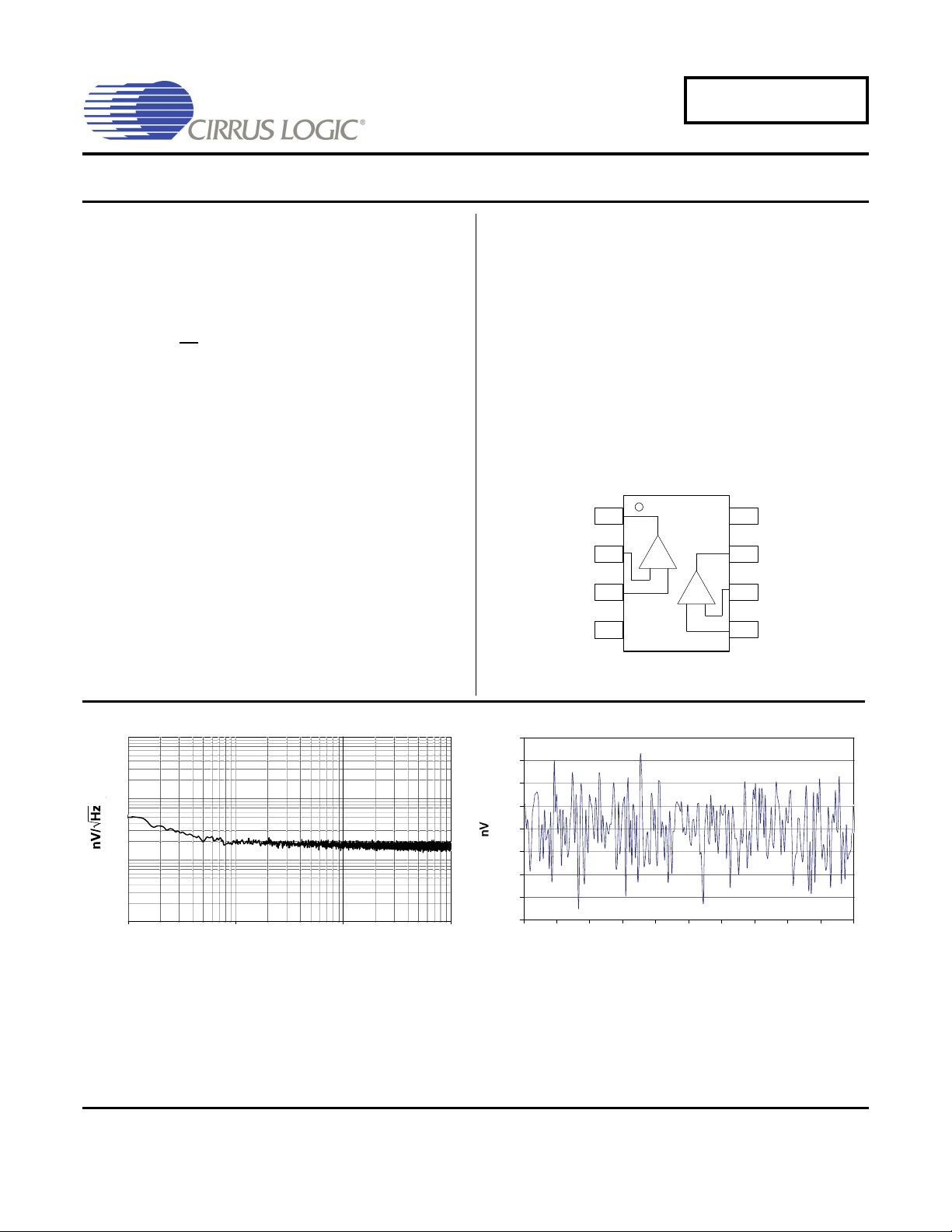
8-Lead SOIC
(Top View)
Out A
-In A
+In A
V-
V+
Out B
-In B
+In B
A
B
-
-
+
+
1
2
3
4
8
7
6
5
1
10
100
1000
0.01 0.1 1 10
Frequency (Hz)
-200
-150
-100
-50
0
50
100
150
200
012345678910
Time (sec)
Noise vs. Frequency (Measured) 0.01 Hz to 10 Hz Noise Performance
CS3004
Features & Description
Low Offset:
–10 μV Max.
Low Drift:
–0.05 μV/°C Max.
Low Noise:
– 17 nV/√Hz
Open-loop Voltage Gain:
– 150 dB Typ.
Rail-to-Rail Inputs
Rail-to-Rail Output Swing
– to within 10 mV of supply voltage
2.1 mA Supply Current
Slew rate:
–0.25 V/μs
Applications
Thermocouple/Thermopile Amplifiers
Load Cell and Bridge Transducer Amplifiers
Precision Instrumentation
Battery-powered Systems
Description
The CS3004 dual amplifier is designed for precision amplification of low-level signals. These amplifiers achieve
excellent offset stability, high open loop gain, and low
noise. The devices also exhibit excellent CMRR and
PSRR. The common mode input range includes the supply rails. The amplifiers operate with any supply voltage
from 2.7 V to 5 V (±1.35 V to ±2.50 V).
Pin Configuration
Cirrus Logic, Inc.
http://www.cirrus.com
Copyright Cirrus Logic, Inc. 2009
(All Rights Reserved)
JUL ‘09
DS719F2
Page 2

TABLE OF CONTENTS
1. CHARACTERISTICS AND SPECIFICATIONS ............................................. 3
1.1 5 V Electrical Characteristics ................................................................... 3
1.2 3 V Electrical Characteristics ................................................................... 4
1.3 Absolute Maximum Ratings ..................................................................... 5
2. TYPICAL PERFORMANCE PLOTS .............................................................. 5
3. PACKAGE DRAWINGS ................................................................................. 7
4. ORDERING INFORMATION .......................................................................... 8
5. ENVIRONMENTAL, MANUFACTURING, & HANDLING INFORMATION ... 8
6. REVISION HISTORY .................................................................................... 9
LIST OF FIGURES
Figure 1. Noise vs Frequency (Measured) .................................................................................5
Figure 2. 0.01 Hz to 10 Hz Noise ................................................................................................5
Figure 3. Gain & Phase vs. Frequency (2.7 V)............................................................................5
Figure 4. Gain & Phase vs. Frequency (5 V) ..............................................................................5
Figure 5. Supply Current vs. Supply Voltage ..............................................................................5
Figure 6. Supply Current vs. Temperature .................................................................................5
Figure 7. Voltage Swing vs. Output Current (2.7 V) ...................................................................6
Figure 8. Voltage Swing vs. Output Current (5 V) .......................................................................6
CS3004
2 DS719F2
Page 3
CS3004
nV/ Hz
nV/ Hz
fA/ Hz
1. CHARACTERISTICS AND SPECIFICATIONS
1.1 5 V Electrical Characteristics
V+ = +5 V, ±5%; V- = 0V; VCM = 2.5 V; Unless otherwise noted,
Parameter Min Typ Max Unit
Input Offset Voltage (Note 2) • -±2±10µV
Average Input Offset Drift (Note 2) • - ±0.01 ±0.05 µV/ºC
Input Bias Current
Input Offset Current
Input Noise Voltage Density R
= 100 Ω, f0 = 1 Hz
S
R
= 100 Ω, f0 = 1 kHz
S
Input Noise Voltage 0.1 to 10 Hz - 350 - nV
Input Noise Current Density f0 = 1 Hz - 100 -
Input Noise Current 0.1 to 10 Hz - 1.9 pA
Input Voltage Range (Note 2) • V- - V+ V
Common Mode Rejection Ratio (dc) • 110 120 - dB
Power Supply Rejection Ratio • 110 130 - dB
Large Signal Voltage Gain
(Note 3)R
Output Voltage Swing R
(Note 4)R
Slew Rate R
= 2 kΩ to V+/2 •
L
= 2 kΩ to V+/2
L
= 100 kΩ to V+/2
L
= 2 k, 100 pF 0.25 - V/µs
L
Overload Recovery Time - 25 - µs
Supply Current • -2.02.5mA
Oscillator Frequency - 150 - kHz
Input Capacitance Differential
Common Mode
TA = 25º C (See Note 1).
-
•
-
-
•
-
±170
±340
-
-
-
120
• (V+ – 100)
(V+ – 10)
-
-
-
-
17
17
150
150
-
-
1.5
10
±250
±1.5
±500
±3.0
-
-
-
-
(V- + 100 )
(V- + 10)
-
-
pA
nA
pA
nA
p-p
p-p
dB
dB
mV
mV
pF
pF
Notes: 1. Symbol “•” denotes specification applies over -40 to +125
° C.
2. This parameter is guaranteed by design and/or laboratory characterization.
3. Guaranteed within the output limits of (V+ – 0.2 V) to (V- + 0.2 V).
4. Specifies the worst case drive voltage relative to the supply rail under stated load conditions.
DS719F2 3
Page 4

CS3004
nV/ Hz
nV/ Hz
fA/ Hz
1.2 3 V Electrical Characteristics
V+ = +3 V, ±10%; V- = 0V; VCM = 2.5 V; Unless otherwise noted,
Parameter Min Typ Max Unit
Input Offset Voltage (Note 6) • -±2±10µV
Average Input Offset Drift (Note 6) • - ±0.01 ±0.05 µV/ºC
Input Bias Current
Input Offset Current
Input Noise Voltage Density R
= 100 Ω, f0 = 1 Hz
S
= 100 Ω, f0 = 1 kHz
R
S
Input Noise Voltage 0.1 to 10 Hz - 350 - nV
Input Noise Current Density f0 = 1 Hz - 100 -
Input Noise Current 0.1 to 10 Hz - 1.9 pA
Input Voltage Range (Note 6) • V- - V+ V
Common Mode Rejection Ratio (dc) • 110 120 - dB
Power Supply Rejection Ratio • 110 130 - dB
Large Signal Voltage Gain
(Note 7)R
Output Voltage Swing R
(Note 8)R
Slew Rate R
= 2 kΩ to V+/2 •
L
= 2 kΩ to V+/2
L
= 100 kΩ to V+/2
L
= 2 k, 100 pF 0.25 - V/µs
L
Overload Recovery Time - 25 - µs
Supply Current • -2.02.5mA
Oscillator Frequency - 150 - kHz
Input Capacitance Differential
Common Mode
TA = 25º C (See Note 5).
-
•
-
-
•
-
-
-
-
120
• (V+ – 100)
(V+ – 10)
-
-
±110
-
±220
-
17
17
160
150
-
-
1.5
10
±150
±1.0
±300
±2.0
-
-
-
-
(V- + 100 )
(V- + 10)
-
-
pA
nA
pA
nA
p-p
p-p
dB
dB
mV
mV
pF
pF
Notes: 5. Symbol “•” denotes specification applies over -40 to +125
° C.
6. This parameter is guaranteed by design and/or laboratory characterization.
7. Guaranteed within the output limits of (V+ – 0.2 V) to (V- + 0.2 V).
8. Specifies the worst case drive voltage relative to the supply rail under stated load conditions.
4 DS719F2
Page 5

CS3004
1
10
100
1000
0.01 0.1 1 10
Frequency (Hz)
Figure 1. Noise vs Frequency (Measured)
Figure 3. Gain & Phase vs. Frequency (2.7 V)
-20
0
20
40
60
80
100
120
140
160
180
-135
-90
-45
0
45
90
135
180
225
270
Frequency (Hz)
0.001 0.1 10 1k 100k 10M0.01 1 100 10k 1M
-180
1.5
1.6
1.7
1.8
1.9
2.0
2.533.544.555.5
Supply voltage
Supply Current (mA)
Figure 5. Supply Current vs. Supply Voltage
Figure 2. 0.01 Hz to 10 Hz Noise
-200
-150
-100
-50
0
50
100
150
200
012345678910
Time (sec)
Figure 4. Gain & Phase vs. Frequency (5 V)
-20
0
20
40
60
80
100
120
140
160
180
Frequency (Hz)
-180
-135
-90
-45
0
45
90
135
180
225
270
0.001 0.1 10 1k 100k 10M0.01 1 100 10k 1M
0.5
1.0
1.5
2.0
2.5
-40 -15 10 35 60 85 110
125
Temperature (°C)
Supply Current (mA)
5V
2.7V
Figure 6. Supply Current vs. Temperature
1.3 Absolute Maximum Ratings
Parameter Min Typ Max Unit
Supply Voltage [(V+) – (V-)]
Input Voltage (V-) – 0.3 - (V+) + 0.3 V
Storage Temperature Range -65 - +150 ºC
2. TYPICAL PERFORMANCE PLOTS
2.7 - 5.5 V
DS719F2 5
Page 6

Typical Performance Plots (Cont.)
-200
-150
-100
-50
V+
V–
+50
+100
+150
+200
01234 5
Output Current (mA)
Output Voltage (mV )
-40°C
+25°C
+125°C
-40°C
+25°C
+125°C
Figure 7. Voltage Swing vs. Output Current (2.7 V)
Figure 8. Voltage Swing vs. Output Current (5 V)
CS3004
V+
-50
-100
-150
-200
+200
+150
Output Voltage (mV )
+100
+50
V–
01234 5
-40°C
+25°C
-40°C
+125°C
+25°C
+125°C
Output Current (mA)
6 DS719F2
Page 7

3. PACKAGE DRAWINGS
8L SOIC (150 MIL BODY) PACKAGE DRAWING
D
H
E
e
b
A1
A
c
L
∝
SEATING
PLANE
1
CS3004
INCHES MILLIMETERS
DIM MIN MAX MIN MAX
A 0.053 0.069 1.35 1.75
A1 0.004 0.010 0.10 0.25
B 0.013 0.020 0.33 0.51
C 0.007 0.010 0.19 0.25
D 0.189 0.197 4.80 5.00
E 0.150 0.157 3.80 4.00
e 0.040 0.060 1.02 1.52
H 0.228 0.244 5.80 6.20
L 0.016 0.050 0.40 1.27
∝
0° 8° 0° 8°
JEDEC # : MS-012
DS719F2 7
Page 8
CS3004
4. ORDERING INFORMATION
Part # Temperature Range Package Description
CS3004-FSZ -40 °C to +125 °C 8-lead SOIC, Lead Free
5. ENVIRONMENTAL, MANUFACTURING, & HANDLING INFORMATION
Model Number Peak Reflow Temp MSL Rating* Max Floor Life
CS3004-FSZ 260 °C 2 365 Days
* MSL (Moisture Sensitivity Level) as specified by IPC/JEDEC J-STD-020.
8 DS719F2
Page 9

6. REVISION HISTORY
Revision Date Changes
PP4 FEB 2007 First public release.
F1 AUG 2007 Updated to “Final” per QPL process.
F2 JUL 2009 Removed lead-containing SOIC & QFN packages from ordering information.
CS3004
DS719F2 9
Page 10

CS3004
Contacting Cirrus Logic Support
For all product questions and inquiries contact a Cirrus Logic Sales Representative.
To find one nearest you go to http://www.cirrus.com
IMPORTANT NOTICE
Cirrus Logic, Inc. and its subsidiaries ("Cirrus") believe that the information contained in this document is accurate and reliable. However, the information is subject
to change without notice and is provided "AS IS" without warranty of any kind (express or implied). Customers are advised to obtain the latest version of relevant
information to verify, before placing orders, that information being relied on is current and complete. All products are sold subject to the terms and conditions of sale
supplied at the time of order acknowledgment, including those pertaining to warranty, indemnification, and limitation of liability. No responsibility is assumed by Cirrus
for the use of this information, including use of this information as the basis for manufacture or sale of any items, or for infringement of patents or other rights of third
parties. This document is the property of Cirrus and by furnishing this information, Cirrus grants no license, express or implied under any patents, mask work rights,
copyrights, trademarks, trade secrets or other intellectual property rights. Cirrus owns the copyrights associated with the information contained herein and gives consent for copies to be made of the information only for use within your organization with respect to Cirrus integrated circuits or other products of Cirrus. This consent
does not extend to other copying such as copying for general distribution, advertising or promotional purposes, or for creating any work for resale.
CERTAIN APPLICATIONS USING SEMICONDUCTOR PRODUCTS MAY INVOLVE POTENTIAL RISKS OF DEATH, PERSONAL INJURY, OR SEVERE PROPERTY OR ENVIRONMENTAL DAMAGE ("CRITICAL APPLICATIONS"). CIRRUS PRODUCTS ARE NOT DESIGNED, AUTHORIZED OR WARRANTED FOR USE
IN PRODUCTS SURGICALLY IMPLANTED INTO THE BODY, AUTOMOTIVE SAFETY OR SECURITY DEVICES, LIFE SUPPORT PRODUCTS OR OTHER CRITICAL APPLICATIONS. INCLUSION OF CIRRUS PRODUCTS IN SUCH APPLICATIONS IS UNDERSTOOD TO BE FULLY AT THE CUSTOMER'S RISK AND
CIRRUS DISCLAIMS AND MAKES NO WARRANTY, EXPRESS, STATUTORY OR IMPLIED, INCLUDING THE IMPLIED WARRANTIES OF MERCHANTABILITY
AND FITNESS FOR PARTICULAR PURPOSE, WITH REGARD TO ANY CIRRUS PRODUCT THAT IS USED IN SUCH A MANNER. IF THE CUSTOMER OR
CUSTOMER'S CUSTOMER USES OR PERMITS THE USE OF CIRRUS PRODUCTS IN CRITICAL APPLICATIONS, CUSTOMER AGREES, BY SUCH USE, TO
FULLY INDEMNIFY CIRRUS, ITS OFFICERS, DIRECTORS, EMPLOYEES, DISTRIBUTORS AND OTHER AGENTS FROM ANY AND ALL LIABILITY, INCLUDING ATTORNEYS' FEES AND COSTS, THAT MAY RESULT FROM OR ARISE IN CONNECTION WITH THESE USES.
Cirrus Logic, Cirrus, and the Cirrus Logic logo designs are trademarks of Cirrus Logic, Inc. All other brand and product names in this document may be trademarks
or service marks of their respective owners.
10 DS719F2
 Loading...