

Page 1
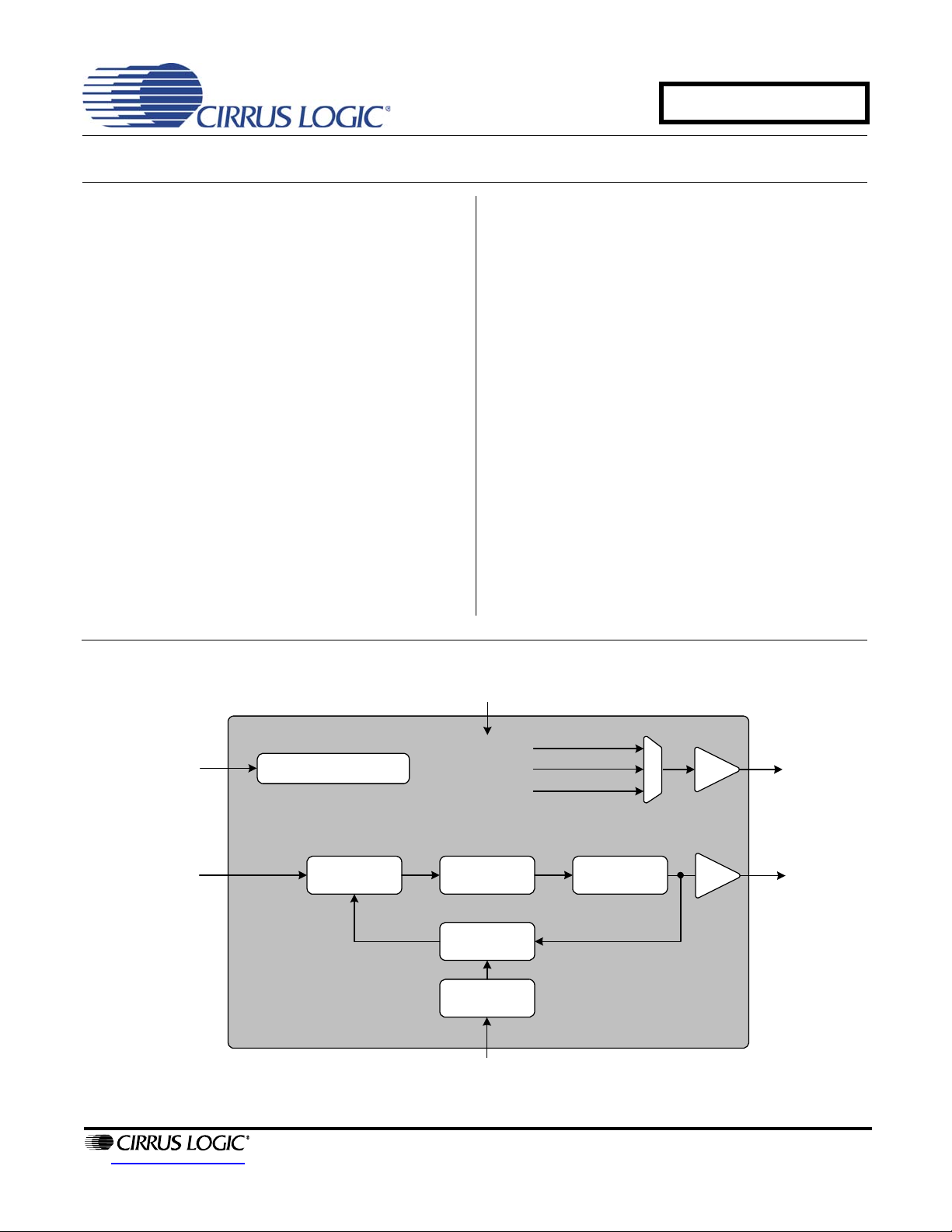
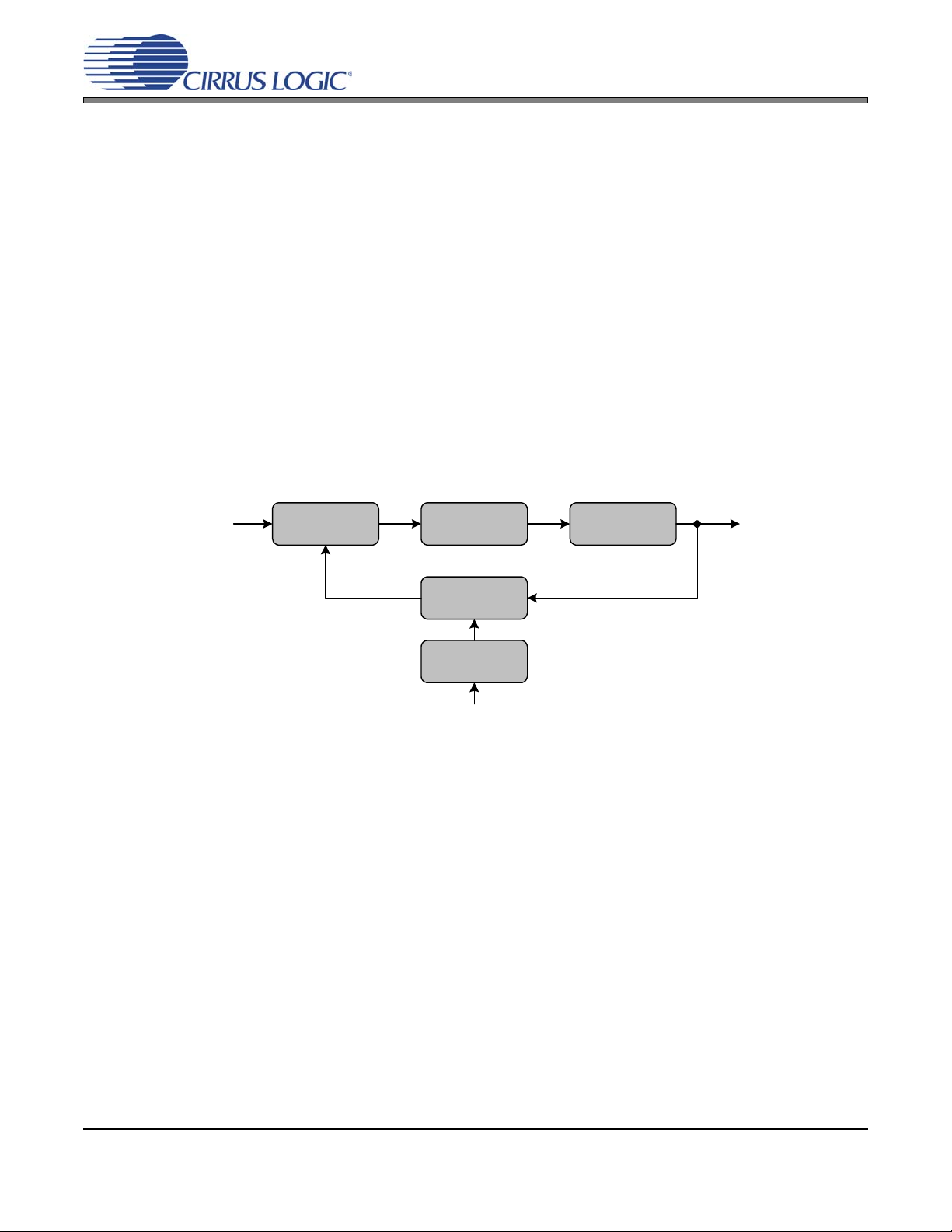
Auxiliary
Output
6 to 75 MHz
PLL Output
3.3 V
8 MHz to 75 MHz
Low-Jitter Timing
Reference
Output to Input
Clock Ratio
N
Timing Reference
PLL Output
PLL Lock Indicator
Fractional-N
Divider
Voltage Controlled
Oscillator
Internal
Loop Filter
Phase
Comparator
Delta-Sigma
Modulator
Hardware Configuration
Hardware Control
CS2200-OTP
Fractional-N Frequency Synthesizer
Features
Delta-Sigma Fractional-N Frequency Synthesis
– Generates a Low Jitter 6 - 75 MHz Clock
Relative to 8 - 75 MHz Reference Clock
Highly Accurate PLL Multiplication Factor
– Maximum Error Less Than 1 PPM
One-Time Programmability
– Configurable Hardware Control Pins
– Configurable Auxiliary Output
Flexible Sourcing of Reference Clock
– External Oscillator or Clock Source
– Supports Inexpensive Local Crystal
Minimal Board Space Required
– No External Analog Loop-filter
Components
General Description
The CS2200-OTP is an extremely versatile system
clocking device that utilizes a programmable phase lock
loop. The CS2200-OTP is based on an analog PLL architecture comprised of a Delta-Sigma Fractional-N
Frequency Synthesizer. This architecture allows for frequency synthesis and clock generation from a stable
reference clock. The CS2200-OTP has many configuration options which are set once prior to runtime. At
runtime there are three hardware configuration pins
available for mode and feature selection.
The CS2200-OTP is available in a 10-pin MSOP package in Commercial (-10°C to +70°C) and Automotive
(-40°C to +85°C) grades. Customer development kits
are also available for custom device prototyp ing, small
production programming, and device evaluation.
Please see “Ordering Information” on page 23 for complete details.
http://www.cirrus.com
Copyright Cirrus Logic, Inc. 2010
(All Rights Reserved)
MAY '10
DS842F2
Page 2

TABLE OF CONTENTS
1. PIN DESCRIPTION ................................................................................................................................. 4
2. TYPICAL CONNECTION DIAGRAM ..................................................................................................... 5
3. CHARACTERISTICS AND SPECIFICATIONS ...................................................................................... 6
RECOMMENDED OPERATING CONDITIONS .................................................................................... 6
ABSOLUTE MAXIMUM RATINGS ........................................................................................................ 6
DC ELECTRICAL CHARACTERISTICS . ... ... .... ... ... ... .... ... ... .................................................................. 6
AC ELECTRICAL CHARACTERISTICS ................................................................................................ 7
4. ARCHITECTURE OVERVIEW ............................................................................................................... 8
4.1 Delta-Sigma Fractional-N Frequency Synthesizer ........................................................................... 8
5. APPLICATIONS ..................................................................................................................................... 9
5.1 One Time Programmability .............................................................................................................. 9
5.2 Timing Reference Clock Input ..................... ..................................................................................... 9
5.2.1 Internal Timing Reference Clock Divider .. ... .... ... ... ... .... ... ... ..................................................... 9
5.2.2 Crystal Connections (XTI and XTO) ...................................................................................... 10
5.2.3 External Reference Clock (REF_CLK) .................................................................................. 10
5.3 Output to Input Frequency Ratio Configuration ............................................................................. 11
5.3.1 User Defined Ratio (RUD) ..................................................................................................... 11
5.3.2 Ratio Modifier (R-Mod) .......................................................................................................... 11
5.3.3 Effective Ratio (REFF) .......................................................................................................... 11
5.3.4 Ratio Configuration Summary ............................................................................................... 12
5.4 PLL Clock Output ........................................................................................................................... 13
5.5 Auxiliary Output ................. ... ... .... ... ... ....................................... ... ... ... .... ......................................... 14
5.6 Mode Pin Functionality ...................... ... ... ....................................... ... .... ... ... ... .... ... ... ...................... 14
5.6.1 M1 and M0 Mode Pin Functionality ....................................................................................... 14
5.6.2 M2 Mode Pin Functionality .................................................................................................... 15
5.6.2.1 M2 Configured as Output Disable .............................................................................. 15
5.6.2.2 M2 Configured as R-Mod Enable .............. ... .... ... ... ....................................... ... ... ... ... 15
5.6.2.3 M2 Configured as AuxOutSrc Override ..................................................................... 15
5.7 Clock Output Stability Considerations ......... ... ... ... .... ... ... ... .... ...................................... ... .... ... ......... 16
5.7.1 Output Switching ................................................................................................................... 16
5.7.2 PLL Unlock Conditions .......................................................................................................... 16
5.8 Required Power Up Sequencing for Programmed Devices .................. ......................................... 16
6. PARAMETER DESCRIPTIONS ........................................................................................................... 17
6.1 Modal Configuration Sets ..................... ... ....................................... ... .... ... ... ... .... ... ... ...................... 17
6.1.1 R-Mod Selection (RModSel[1:0]) ........................ ...... ....... ...... ....... ...... ....... ...... ...... ....... ...... ...17
6.1.2 Auxiliary Output Source Selection (AuxOutSrc[1:0]) .................... ......................................... 18
6.2 Ratio 0 - 3 .. ... ....................................... ... .... ...................................... .... ... ...................................... 18
6.3 Global Configuration Parameters ................................................................................................... 18
6.3.1 AUX PLL Lock Output Configuration (AuxLockCfg) .............................................................. 18
6.3.2 Reference Clock Input Divider (RefClkDiv[1:0]) .................................................................... 18
6.3.3 Enable PLL Clock Output on Unlock (ClkOutUnl) ................................................................. 19
6.3.4 M2 Pin Configuration (M2Config[2:0]) ................................................................................... 19
7. CALCULATING THE USER DEFINED RATIO .................................................................................... 20
7.1 12.20 Format ........................ ... ....................................... ... .... ... ... ... ................................................ 20
8. PROGRAMMING INFORMATION ....................................................................................................
9. PACKAGE DIMENSIONS .................................................................................................................... 22
THERMAL CHARACTERISTICS ......................................................................................................... 22
10. ORDERING INFORMATION ........... ... ... ... ... .... ... ....................................... ... ... ... .... ... ... ... ... .... ... ......... 23
11. REVISION HISTORY ................................ ... .... ... ....................................... ... ... ... .... ... ... ... ................... 23
CS2200-OTP
.... 21
LIST OF FIGURES
Figure 1. Typical Connection Diagram ........................................................................................................ 5
DS842F2 2
Page 3

Figure 2. Delta-Sigma Fractional-N Frequency Synthesizer .......................................................................8
Figure 3. Internal Timing Reference Clock Divider ..................................................................................... 9
Figure 4. REF_CLK Frequency vs. a Fixed CLK_OUT ............................................................................. 10
Figure 5. External Component Requirements for Crystal Circuit .............................................................. 10
Figure 6. Ratio Feature Summary ............................................................................................................. 12
Figure 7. PLL Clock Output Options ......................................................................................................... 13
Figure 8. Auxiliary Output Selection .......................................................................................................... 14
Figure 9. M2 Mapping Options .................................................................................................................. 15
Figure 10. Parameter Configuration Sets .................................................................................................. 17
LIST OF TABLES
Table 1. Modal and Global Configuration ........................ .... ... ... ... .... ... ... ... ... .... ... ........................................ 9
Table 2. Ratio Modifier .............................................................................................................................. 11
Table 3. Example 12.20 R-Values ............................................................................................................ 20
CS2200-OTP
DS842F2 3
Page 4

1. PIN DESCRIPTION
1
2
3
4
5
6
7
8
9
10
XTO
CLK_OUT
GND
VD
XTI/REF_CLK
M2
M1
M0
AUX_OUT
TST_IN
Pin Name # Pin Description
VD 1 Digital Power (Input) - Positive power supply for the digital and analog sections.
GND 2 Ground (Input) - Ground reference.
CLK_OUT 3 PLL Clock Output (Output) - PLL clock output.
AUX_OUT 4
TST_IN
XTO
XTI/REF_CLK
M2 8 Mode Select (Input) - M2 is a configurable mode selection pin.
M1 9 Mode Select (Input) - M1 is a configurable mode selection pin.
M0 10 Mode Select (Input) - M0 is a configurable mode selection pin.
Auxiliary Output (Output) - This pin outputs a buffered version of one of the input or output clocks,
or a status signal, depending on configuration.
5 Test Input (Input) - This pin is for factory test purposes and must be connected to GND for proper
operation.
Crystal Connections (XTI/XTO) / Timing Reference Clock Input (REF_CLK) (Input/Output) -
6
XTI/XTO are I/O pins for an external crystal which may be used to generate the low-jitter PLL input
7
clock. REF_CLK is an input for an externally generated low-jitter reference clock.
CS2200-OTP
4 DS842F2
Page 5
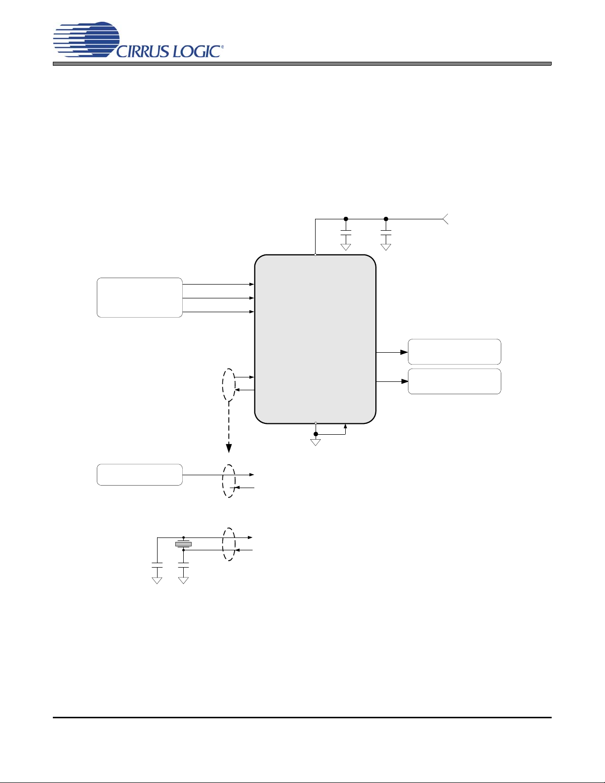
2. TYPICAL CONNECTION DIAGRAM
2
1
GND
M2
M1
XTI/REF_CLK
TST_IN
XTO
CLK_OUT
AUX_OUT
0.1 µF
VD
+3.3 V
M0
Low-Jitter
Timing Reference
System Microcontroller
1 µF
1
or
2
REF_CLK
XTO
XTI
XTO
or
40 pF
x
40 pF
Crystal
To circuitry which requires
a low-jitter clock
N.C.
To other circuitry or
Microcontroller
Figure 1. Typical Connection Diagram
CS2200-OTP
CS2200-OTP
DS842F2 5
Page 6
CS2200-OTP
3. CHARACTERISTICS AND SPECIFICATIONS
RECOMMENDED OPERATING CONDITIONS
GND = 0 V; all voltages with respect to ground. (Note ?)
Parameters Symbol Min Typ Max Units
DC Power Supply VD 3.1 3.3 3.5 V
Ambient Operating Temperature (Power Applied)
Commercial Grade
Automotive Grade
T
AC
T
AD
-10
-40
-
-
+70
+85
°C
°C
Notes: 1. Device functionality is not guaranteed or implied outside of these limits. Operation outside of these limits
may adversely affect device reliability.
ABSOLUTE MAXIMUM RATINGS
GND = 0 V; all voltages with respect to ground.
Parameters Symbol Min Max Units
DC Power Supply VD -0.3 6.0 V
Input Current I
Digital Input Voltage (Note 3)V
Ambient Operating Temperature (Power Applied) T
Storage Temperature T
IN
IN
A
stg
-±10mA
-0.3 VD + 0.4 V
-55 125 °C
-65 150 °C
WARNING:Operation at or beyond these limits may result in permanent damage to the device.
Notes: 2. The maximum over/under voltage is limited by the input current except on the power supply pin.
DC ELECTRICAL CHARACTERISTICS
Test Conditions (unless otherwise specified): VD = 3.1 V to 3.5 V; TA = -10°C to +70°C (Commercial Grade);
T
= -40°C to +85°C (Automotive Grade).
A
Parameters Symbol Min Typ Max Units
Power Supply Current - Unloaded (Note 4)I
Power Dissipation - Unloaded (Note 4)P
Input Leakage Current I
Input Capacitance I
High-Level Input Voltage V
Low-Level Input Voltage V
High-Level Output Voltage (I
Low-Level Output Voltage (I
= -1.2 mA) V
OH
= 1.2 mA) V
OH
D
D
IN
C
IH
IL
OH
OL
Notes: 3. To calculate the additional current consumption due to loading (per output pin), multiply clock output
frequency by load capacitance and power supply voltage.
For example,
f
CLK_OUT
(49.152 MHz) * CL (15 pF) * VD (3.3 V) = 2.4 mA of additional current due to
these loading conditions on CLK_OUT.
-1218mA
-4060mW
--±10µA
-8-pF
70% - - VD
--30%VD
80% - - VD
--20%VD
6 DS842F2
Page 7
CS2200-OTP
AC ELECTRICAL CHARACTERISTICS
Test Conditions (unless otherwise specified): VD = 3.1 V to 3.5 V; TA = -10°C to +70°C (Commercial Grade);
= -40°C to +85°C (Automotive Grade); CL=15pF.
T
A
Parameters Symbol Conditions Min Typ Max Units
Crystal Frequency
Fundamental Mode XTAL
Reference Clock Input Frequency f
Reference Clock Input Duty Cycle D
Internal System Clock Frequency f
PLL Clock Output Frequency f
PLL Clock Output Duty Cycle t
Clock Output Rise Time t
Clock Output Fall Time t
Period Jitter t
Base Band Jitter (100 Hz to 40 kHz) (Notes 10, 11) - 50 - ps rms
Wide Band JItter (100 Hz Corner) (Notes 10, 12) - 175 - ps rms
PLL Lock Time - REF_CLK t
Output Frequency Synthesis Resolution (Note 15)f
f
XTAL
REF_CLK
REF_CLK
SYS_CLK
CLK_OUT
OD
OR
OF
JIT
LR
err
RefClkDiv[1:0] = 10
RefClkDiv[1:0] = 01
RefClkDiv[1:0] = 00
RefClkDiv[1:0] = 10
RefClkDiv[1:0] = 01
RefClkDiv[1:0] = 00
Measured at VD/2 45 50 55 %
20% to 80% of VD - 1.7 3.0 ns
80% to 20% of VD - 1.7 3.0 ns
(Note 10) - 70 - ps rms
f
REF_CLK
= 8 to 75 MHz - 1 3 ms
8
16
32
8
16
32
45 - 55 %
814MHz
6-75MHz
0-±0.5ppm
-
-
-
-
-
-
14
28
50
14
28
56
MHz
MHz
MHz
MHz
MHz
MHz
Notes: 4.
f
CLK_OUT
= 24.576 MHz; Sample size = 10,000 points; AuxOutSrc[1:0] =11.
5. In accordance with AES-12id-2006 section 3.4.2. Measurements are Time Inte rval Error taken with 3rd
order 100 Hz to 40 kHz bandpass filter.
6. In accordance with AES-12id-2006 section 3.4.1. Measurements are Time Inte rval Error taken with 3rd
order 100 Hz Highpass filter.
7. The frequency accuracy of the PLL clock output is directly proportional to the frequency accuracy of the
reference clock.
DS842F2 7
Page 8
4. ARCHITECTURE OVERVIEW
Fractional-N
Divider
Timing Reference
Clock
PLL Output
Voltage Controlled
Oscillator
Internal
Loop Filter
Phase
Comparator
N
Delta-Sigma
Modulator
4.1 Delta-Sigma Fractional-N Frequency Synthesizer
The core of the CS2200 is a Delta-Sigma Fractional-N Frequency Synthesizer which has very high-resolution for Input/Output clock ratios, low phase noise, very wide range of output frequencies and the ability to
quickly tune to a new frequency. In very simplistic terms, the Fractional-N Freq uency Synthesizer multiplies
the Timing Reference Clock by the value of N to generate the PLL out put clock. The desired output to input
clock ratio is the value of N that is applied to the delta-sigma modulator (see Figure 2).
The analog PLL based frequency synthesizer uses a low-jitter timing reference clock as a time and phase
reference for the internal voltage controlled oscillator (VCO). The phase comparator compares the fractional-N divided clock with the original timing reference and generates a control signal. The control signal is filtered by the internal loop filter to generate the VCO’s control voltage which sets its output frequency. The
delta-sigma modulator modulates the loop integer divide ratio to get the desired fractional ratio betwee n the
reference clock and the VCO output (thus the duty cycle of the modulator sets the fractional value). This
allows the design to be optimized for very fast lock times for a wide rang e of outpu t freq uencies withou t the
need for external filter components. As with any Fractional-N Frequency Synthesizer the timing reference
clock should be stable and jitter-free.
CS2200-OTP
8 DS842F2
Figure 2. Delta-Sigma Fractional-N Frequency Synthesizer
Page 9

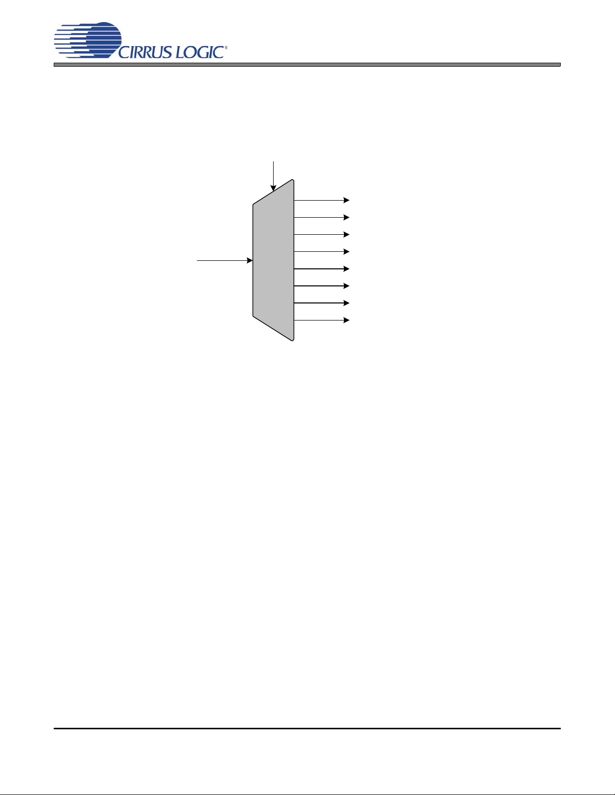
5. APPLICATIONS
Figure 3. Internal Timing Reference Clock Divider
N
Internal Timing
Reference Clock
PLL Output
Fractional-N
Frequency
Synthesizer
Timing Reference
Clock Divider
÷1
÷2
÷4
XTI/REF_CLK
RefClkDiv[1:0]
8 MHz < SysClk < 14 MHz
8 MHz < RefClk <
Timing Reference Clock
50 MHz (XTI)
58 MHz (REF_CLK)
5.1 One Time Programmability
The one time programmable (OTP) circuitry in the CS2200-OTP allows for pre-configuration of the device
prior to use in a system. There are two types of parameter s that are used for device pre-configuration: modal
and global. The modal parameters are features which, when grouped tog ether, create a modal configuration
set (see Figure 10 on page 17). Up to four modal configuration sets can be permanently stored and then
dynamically selected using the M[1:0] mode select pins (see Table 1). The global parameters are the re-
maining configuration settings which do not change with the mode select pins. The modal and global parameters can be pre-set at the factory or user progr ammed using the customer deve lopment kit, CDK20 00;
Please see “Programming Information” on page 21 for more details.
Parameter Type M[1:0] pins = 00 M[1:0] pins = 01 M[1:0] pins = 10 M[1:0] pins = 11
Modal Configuration Set 0
Ratio 0
Global Configuration settings set once for all modes.
Table 1. Modal and Global Configuration
5.2 Timing Reference Clock Input
Configuration Set 1
Ratio 1
Configuration Set 2
Ratio 2
CS2200-OTP
Configuration Set 3
Ratio 3
The low jitter timing reference clock (RefClk) can be provided by either an external reference clock or an
external crystal in conjunction with the internal oscillator. In order to maintain a stable and low-jitter PLL output the timing reference clock must also be stable and low-jitter; the quality of the timing reference clock
directly affects the performance of the PLL and hence the quality of the PLL output.
5.2.1 Internal Timing Reference Clock Divider
The Internal Timing Reference Clock (SysClk) is limited to a lower maximum frequency than that allowed
on the XTI/REF_CLK pin. The CS2200-OTP supports the wider external frequency range by offering an
internal divider for RefClk. The RefClkDiv[1:0] global parameter should be configured such that SysClk,
the divided RefClk, then falls within the valid range as indicated in “AC Electrical Characteristics” on
page 7.
It should be noted that the maximum allowable input frequency of the XTI/REF_CLK pin is dependent
upon its configuration as either a crystal connection or external clock input. See the “AC Electrical Char-
acteristics” on page 7 for more details.
For the lowest possible output jitter, attention should be paid to th e absolute frequency of the Timing Reference Clock relative to the PLL Output frequency ( CLK_OUT ). To minimize outp ut jitter, the Timing Reference Clock frequency should be chosen such that f
where N is an integer. Figure 4 shows the effect of varying the RefClk frequency around f
is at least +/-15 kHz from f
RefClk
CLK_OUT
CLK_OUT
*N/32
*N/32.
It should be noted that there will be a jitter null at the zero point when N = 32 (not shown in Figure 4). An
DS842F2 9
Page 10
CS2200-OTP
-80 -60 -40 -20 0 20 40 60 80
20
40
60
80
100
120
140
160
180
Normalized REF__CLK Frequency (kHz)
Typical Base Band Jitter (psec)
CLK__OUT Jitt er
-15 kHz +15 kHz
CLK__OUT
f
*32/N
Figure 4. REF_CLK Frequency vs. a Fixed CLK_OUT
fLf
RefClkfH
≤≤
fLf
CLK_OUT
31
32
----- -
15kHz+×=
12.288MHz 0.96875 15kHz+×=
11.919MHz=
fHf
CLK_OUT
32
32
----- -
15kHz–×=
12.288MHz 115kHz+×=
12.273MHz=
XTI XTO
40 pF 40 pF
Figure 5. External Component Requirements for Crystal Circuit
example of how to determine the range of RefClk frequencies around 12 MHz to be used in order to
achieve the lowest jitter PLL output at a frequency of 12.288 MHz is as follows:
where:
and
Referenced Control Parameter Definition
RefClkDiv[1:0].......................“Reference Clock Input Divider (RefClkDiv[1:0])” on page 18
5.2.2 Crystal Connections (XTI and XTO)
An external crystal may be used to generate RefClk. To accomplish this, a 20 pF fundamental mode parallel resonant crystal must be connected between the XTI and XTO pins as shown in Figure 5. As shown,
nothing other than the crystal and its load capacitors should be connected to XTI and XTO. Please refer
to the “AC Electrical Characteristics” on page 7 for the allowed crystal frequency range.
5.2.3 External Reference Clock (REF_CLK)
For operation with an externally generated REF_CLK signal, XTI/REF_CLK should be connected to the
reference clock source and XTO should be left unconnected or terminated through a 47 kΩ resistor to
GND.
10 DS842F2
Page 11

5.3 Output to Input Frequency Ratio Configuration
5.3.1 User Defined Ratio (RUD)
The User Defined Ratio, RUD, is a 32-bit un-signed fixed-point number which determines the basis for the
desired input to output clock ratio. Up to four different ratios, Ratio
time programmable memory. Selection between the four ratios is achieved by the M[1:0] mode select
pins. The 32-bit R
is represented in a 12.20 format where the 12 MSBs represent the integer binary
UD
portion while the remaining 20 LSBs represent the fractional binary portion. The maximum multiplication
factor is approximately 4096 with a resolution of 0.954 PPM in this configuration. See “Calculating the
User Defined Ratio” on page 20 for more information.
The status of internal dividers, such as the internal timing reference clock divider, are automatically taken
into account. Therefore R
Referenced Control Parameter Definition
Ratio 0-3................................“Ratio 0 - 3” on page 18
M[1:0]....................................“M1 and M0 Mode Pin Functionality” on page 14
is simply the desired ratio of the output to input clock frequencies.
UD
5.3.2 Ratio Modifier (R-Mod)
CS2200-OTP
, can be stored in the CS2200’s one
0-3
The Ratio Modifier is used to internally multiply/divide the currently ad dressed RUD (Ratio
register space remain unchanged). The available options for R-Mod are summarized in Table 2 on
page 11. R-Mod is enabled via the M2 pin in conjunction with the appropriate setting of the M2Config[2:0]
global parameter (see Section 5.6.2 on page 15).
Referenced Control Parameter Definition
Ratio 0-3................................“Ratio 0 - 3” on page 18
RModSel[1:0] ........................“R-Mod Selection (RModSel[1:0])” section on page 17
M2Config[2:0]........................“M2 Pin Configuration (M2Config[2:0])” on page 19
5.3.3 Effective Ratio (R
The Effective Ratio (R
previously described. R
R
= RUD • R-Mod
EFF
stored in the
0-3
RModSel[1:0] R Modifier
00 0.5
01 0.25
10 0.125
11 0.0625
Table 2. Ratio Modifier
)
EFF
) is an internal calculation comprised of RUD and the appropriate modifiers, as
EFF
is calculated as follows:
EFF
To simplify operation the device handles some of the ratio calculation functions automatically (such as
when the internal timing reference clock divider is set). For this reason, the Effective Ratio does not need
to be altered to account for internal dividers.
Ratio modifiers which would produce an overflow or truncation of R
the maximum and minimum allowable values for R
are dictated by the frequency limits for both the
EFF
should not be used. In all cases,
EFF
input and output clocks as shown in the “AC Electrical Characteristics” on page 7.
DS842F2 11
Page 12

Selection of the user defined ratio from the four stored ratios is made by using the M[1:0] pins.
Effective Ratio R
EFF
Ratio Format
SysClk
PLL Output
Frequency
Synthesizer
Ratio 0
Ratio 1
Ratio 2
Ratio 3
12.20
M[1:0] pins
RModSel[1:0]
4
Ratio
Modifier
R Correction
RefClkDiv[1:0]
Timing Reference Clock
(XTI/REF_CLK)
Divide
RefClkDiv[1:0]
Static Ratio, ‘N’
User Defined Ratio R
UD
M2 pin
Referenced Control Parameter Definition
M[1:0] pins.............................“M1 and M0 Mode Pin Functionality” on page 14
5.3.4 Ratio Configuration Summary
CS2200-OTP
The RUD is the user defined ratio for which up to four different values (Ratio
) can be stored in the one
0-3
time programmable memory. The M[1:0] pins then select the user defined ratio to be used as well as the
modal configuration set. R-Mod is applied accordingly. The user defined ratio and ratio modifier make up
the effective ratio R
, the final calculation used to determine the output to input clock ratio. The effective
EFF
ratio is then corrected for the internal dividers. The conceptual diagram in Figure 6 summarizes the fea-
tures involved in the calculation of the ratio va lues us ed to ge nerate the fractiona l-N value which con trols
the Frequency Synthesizer. The subscript ‘4’ indicates the modal parameters.
Figure 6. Ratio Feature Summary
Referenced Control Parameter Definition
Ratio 0-3................................“Ratio 0 - 3” on page 18
M[1:0] pins.............................“M1 and M0 Mode Pin Functionality” on page 14
RModSel[1:0] ........................“R-Mod Selection (RModSel[1:0])” section on page 17
RefClkDiv[1:0].......................“Reference Clock Input Divider (RefClkDiv[1:0])” on page 18
12 DS842F2
Page 13

5.4 PLL Clock Output
PLL Locked/Unlocked
PLL Output
2:1 Mux
M2 pin with
M2Config[1:0] = 000, 010
2:1 Mux
ClkOutUnl
0
PLL Clock Output Pin
(CLK_OUT)
0
1
0
1
PLL Clock Output
PLLClkOut
The PLL clock output pin (CLK_OUT) provides a buffered version of the outp ut of the frequency synthesizer.
The driver can be set to high-impedance with the M2 p in when the M2Config[1:0] global parameter is set to
either 000 or 010. The output from the PLL automatically drives a static low condition while the PLL is unlocked (when the clock may be unreliable ). This feature can be disabled by setting the ClkOutUnl global
parameter, however the state CLK_OUT may then be unreliable during an unlock condition.
Referenced Control Parameter Definition
ClkOutUnl..............................“Enable PLL Clock Output on Unlock (ClkOutUnl)” on page 19
ClkOutDis..............................“M2 Configured as Output Disable” on page 15
M2Config[2:0]........................“M2 Pin Configuration (M2Config[2:0])” on page 19
CS2200-OTP
Figure 7. PLL Clock Output Options
DS842F2 13
Page 14
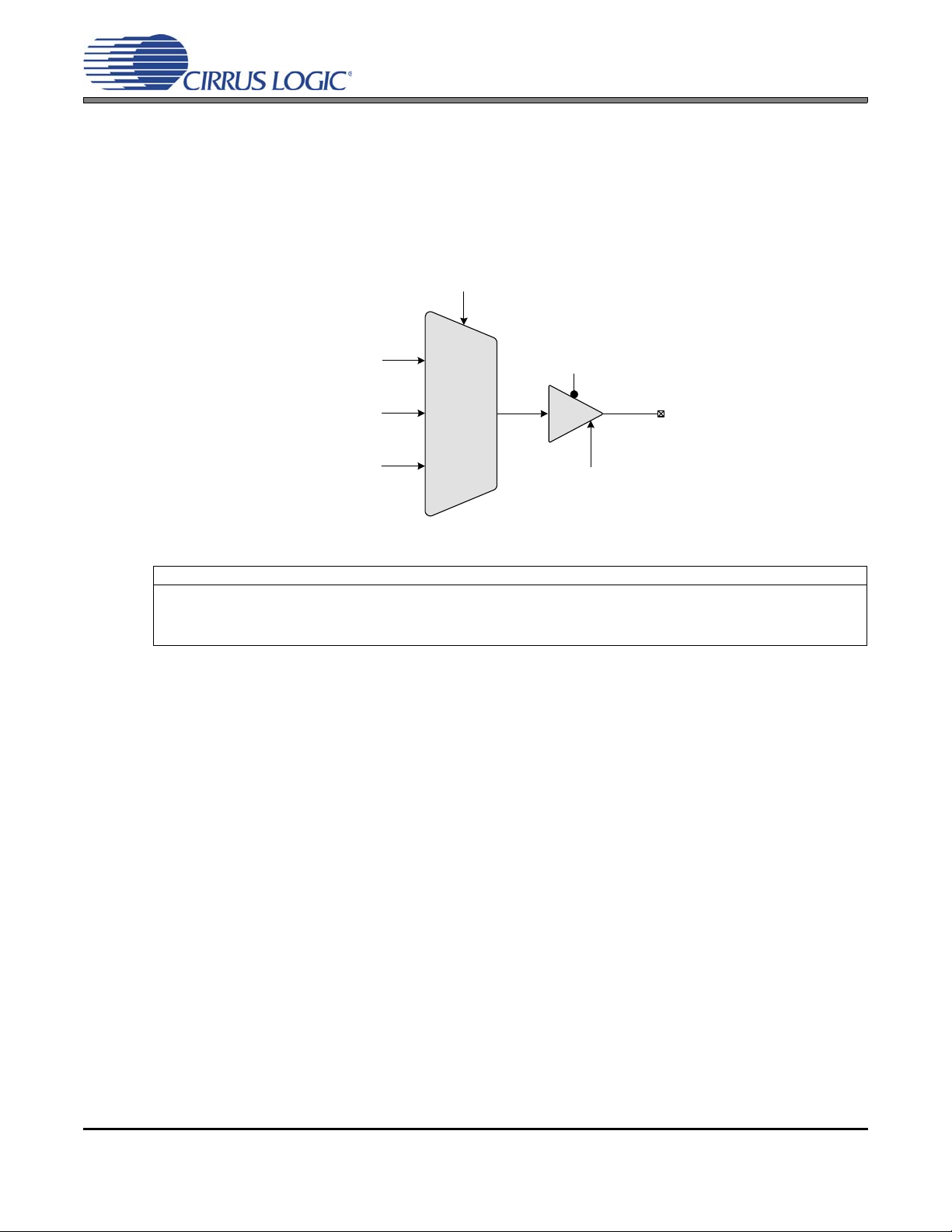
5.5 Auxiliary Output
3:1 Mux
Auxiliary Output Pin
(AUX_OUT)
AuxOutDis
AuxOutSrc[1:0]
AuxLockCfg
Timing Reference Clock
(RefClk)
PLL Clock Output
(PLLClkOut)
PLL Lock/Unlock Indicat i on
(Lock)
The auxiliary output pin (AUX_OUT) can be mapped, as shown in Figure 8, to one of three signals: reference clock (RefClk), additional PLL clock output (CLK_OUT) , or a PLL lock indicator (Lock). The mux is controlled via the AuxOutSrc[1:0] modal parameter. If AUX_OUT is set to Lock, the AuxLockCfg global
parameter is then used to control the output driver type and polarity of the LOCK signal (see section 6.3.1
on page 18). If AUX_OUT is set to CLK_OUT, the phase of the PLL Clock Output signal on AUX_OUT may
differ from the CLK_OUT pin. The driver for the pin can be set to high-impedance using the M2 pin when
the M2Config[1:0] global parameter is set to either 001 or 010.
CS2200-OTP
Figure 8. Auxiliary Output Selection
Referenced Control Parameter Definition
AuxOutSrc[1:0]......................“Auxiliary Output Source Selection (AuxOutSrc[1:0])” on page 18
AuxOutDis.............................“M2 Configured as Output Disable” on page 15
AuxLockCfg...........................“AUX PLL Lock Output Configuration (AuxLockCfg)” section on page 18
M2Config[2:0]........................“M2 Pin Configuration (M2Config[2:0])” on page 19
5.6 Mode Pin Functionality
5.6.1 M1 and M0 Mode Pin Functionality
M[1:0] determine the functional mode of the device and select both the default User Defined Ratio and
the set of modal parameters. The modal parameters are RModSel[1:0] and AuxOutSrc[1:0]. By modifying
one or more of the modal parameters between the 4 sets, different functional configurations can be
achieved. However, global parameters are fixed and the same value will be applied to each functional
configuration. Figure 10 on page 17 provides a summary of all parameters used by the device.
14 DS842F2
Page 15
5.6.2 M2 Mode Pin Functionality
M2 pin
Disable CLK_OUT and AUX_OUT pins
Disable AUX_OUT pin
Disable CLK_OUT pin
RModSel[1:0] Modal Parameter Enable
Force AuxOutSel[1:0] = 10 (PLL Clock Out)
Reserved
Reserved
M2Config[2:0] global parameter
000
001
010
011
100
101
110
111
Reserved
M2 usage is mapped to one of the optional special functions via the M2Config[2:0] g lobal parameter . Depending on what M2 is mapped to, it will either act as an output enable/disable pin or override certain modal parameters. Figure 9 summarizes the available options and the following sections will describe each
option in more detail.
CS2200-OTP
Figure 9. M2 Mapping Options
5.6.2.1 M2 Configured as Outpu t Disable
If M2Config[2:0] is set to either ‘000’, ‘001’, or ‘010’, M2 becomes an output disable pin for one or
both output pins. If M2 is driven ‘low’, the corresponding output(s) will be enabled, if M2 is driven
‘high’, the corresponding output(s) will be disabled.
5.6.2.2 M2 Configured as R-Mod Enable
If M2Config[2:0] is set to ‘011’, M2 becomes the R-Mod enable pin. It should be noted that M2 is
the only way to enable R-Mod. Even though the RModSel[1:0] modal parameter can be set arbi-
trarily for each configuration set, it will not take effect unless enabled via M2. If M2 is driven ‘low’,
R-Mod will be disabled, if M2 is driven ‘high’ R-Mod will be enabled.
5.6.2.3 M2 Configured as AuxOutSrc Override
If M2Config[2:0] is set to ‘111’, M2 when driven ‘high’ will override the AuxOutSrc[1:0] modal parameter and force the AUX_OUT source to PLL Clock Output . Wh en M2 is driven ‘low’, AUX_OUT
will function according to AuxOutSrc[1:0].
DS842F2 15
Page 16

5.7 Clock Output Stability Considerations
5.7.1 Output Switching
The CS2200-OTP is designed such that re-configuration of the clock routing functions do not result in a
partial clock period on any of the active outputs (CLK_OUT and/or AUX_OUT). In particular, enabling or
disabling an output, changing the auxiliary output source between REF_CLK and CLK_OUT, and the automatic disabling of the output(s) during unlock will not cause a runt or partial clock period.
The following exceptions/limitations exist:
• Enabling/disabling AUX_OUT when AuxOutSrc[1:0] = 11 (unlock indicator).
• Switching AuxOutSrc[1:0] to or from 11 (unlock indicator)
(Transitions between AuxOutSrc[1:0] = [00,10] will not produce a glitch).
When any of these exceptions occur, a partial clock period on the output may result.
5.7.2 PLL Unlock Conditions
Certain changes to the clock inputs and mode pins can cause the PLL to lose lock which will affect the
presence of a clock signal on CLK_OUT. The following outlin es which conditions ca use the PLL to go unlocked:
CS2200-OTP
• Any change in the state of the M1 and M0 pins will cause the PLL to temporarily lose lock as the new
setting takes affect .
• Changes made to the state of the M2 when the M2Config[2:0] global parameter is set to 011, 100, 101,
or 110 can cause the PLL to temporarily lose lock as the new setting takes affect.
• Any discontinuities on the Timing Reference Clock, REF_CLK.
5.8 Required Power Up Sequencing for Programmed Devices
• Apply power. All input pins, except XTI/REF_CLK, should be held in a static logic hi or lo state until the
DC Power Supply specification in the “Recommended Operating Conditions” table on page 6 are met.
• Apply input clock.
• For CDK programmed devices, toggle the state of the M0, M1, or both pins at least 3 times to initialize
the device. This must be done after the power supply is stable and before normal operation is expected.
Note:This operation is not required for factory programmed devices.
• After the specified PLL lock time on page 7 has passed, the device will output the desired clock as configured by the M0-M2 pins.
16 DS842F2
Page 17

CS2200-OTP
M[1:0] pins
Modal Configuration Set #0
RModSel[1:0] AuxOutSrc[1:0]
Modal Configuration Set #1
Ratio 1 RModSel[1:0] AuxOutSrc[1:0]
Modal Configuration Set #2
Ratio 2 RModSel[1:0] AuxOutSrc[1:0]
Modal Configuration Set #3
Ratio 3 RModSel[1:0] AuxOutSrc[1:0]
00
01
10
11
Global Configuration Set
RefClkDiv[1:0] ClkOutUnlAuxLockCfg M2Config[2:0]
Ratio 0
Digital/PLL Core
6. PARAMETER DESCRIPTIONS
As mentioned in Section 5.1 on page 9, there are two different kinds of parameter configuration sets, Modal and
Global. These configuration sets, shown in Figure 10, can be programmed in the field using the CDK2000 or preprogrammed at the factory. Please see “Programming Information” on page 21 for more details.
6.1 Modal Configuration Sets
6.1.1 R-Mod Selection (RModSel[1:0])
Figure 10. Parameter Configuration Sets
There are four instances of each of these configuration parameters. Sele ction between the four stored sets
is made using the M[1:0] pins.
Selects the R-Mod value, which is used as a factor in determining the PLL’s Fractional N.
RModSel[1:0] R-Mod Selection
00 Right-shift R-value by 1 (÷ 2).
01 Right-shift R-value by 2 (÷ 4).
10 Right-shift R-value by 3 (÷ 8).
11 Right-shift R-value by 4 (÷ 16).
Application: “Ratio Modifier (R-Mod)” on page 11
Note: This parameter does not take affect unless M2 pin is high and the M2Config[2:0] global param-
eter is set to ‘011’.
DS842F2 17
Page 18

6.1.2 Auxiliary Output Source Selection (AuxOutSrc[1:0])
Selects the source of the AUX_OUT signal.
AuxOutSrc[1:0] Auxiliary Output Source
00 RefClk.
01 Reserved.
10 CLK_OUT.
11 PLL Lock Status Indicator.
Application: “Auxiliary Output” on page 14
Note: When set to 11, the AuxLockCfg global parameter sets the polarity and driver type (“AUX PLL
Lock Output Configuration (AuxLockCfg)” on page 18).
6.2 Ratio 0 - 3
The four 32-bit User Defined Ratios are stored in the CS220 0’s one time programmable memo ry. See “Out-
put to Input Frequency Ratio Configuration” on page 11 and “Calculating the User Defined Ratio” on
page 20 for more details.
6.3 Global Configuration Parameters
6.3.1 AUX PLL Lock Output Configuration (AuxLockCfg)
CS2200-OTP
When the AUX_OUT pin is configured as a lock indicator (AuxOutSrc[1:0] modal parameter = ‘11’), this
global parameter configures the AUX_OUT driver to either push-pull or op en drain. It also determines the
polarity of the lock signal. If AUX_OUT is configured as a clock output, the state of this parameter is disregarded.
AuxLockCfg AUX_OUT Driver Configuration
0 Push-Pull, Active High (output ‘high’ for unlocked condition, ‘low’ for locked condition).
1 Open Drain, Active Low (output ‘low’ for unlocked condition, high-Z for locked condition).
Application: “Auxiliary Output” on page 14
Note: AUX_OUT is an unlock indicator, signalling an error condition when the PLL is u nlocked. There-
fore, the pin polarity is defined relative to the unlock condition.
6.3.2 Reference Clock Input Divider (RefClkDiv[1:0])
Selects the input divider for the timing reference clock.
RefClkDiv[1:0] Reference Clock Input Divider REF_CLK Frequency Range
00 ÷ 4. 32 MHz to 56 MHz (50 MHz with XTI)
01 ÷ 2. 16 MHz to 28 MHz
10 ÷ 1. 8 MHz to 14 MHz
11 Reserved.
Application: “Internal Timing Reference Clock Divider” on page 9
18 DS842F2
Page 19

6.3.3 Enable PLL Clock Output on Unlock (ClkOutUnl)
Defines the state of the PLL output during the PLL unlock condition.
ClkOutUnl Clock Output Enable Status
0 Clock outputs are driven ‘low’ when PLL is unlocked.
1 Clock outputs are always enabled (results in unpredictable output when PLL is unlocked).
Application: “PLL Clock Output” on page 13
6.3.4 M2 Pin Configuration (M2Config[2:0])
Controls which special function is mapped to the M2 pin.
M2Config[2:0] M2 pin function
000 Disable CLK_OUT pin.
001 Disable AUX_OUT pin.
010 Disable CLK_OUT and AUX_OUT.
011 RModSel[1:0] Modal Parameter Enable.
100 Reserved.
101 Reserved.
110 Reserved.
111 Force AuxOutSrc[1:0] = 10 (PLL Clock Out).
Application: “M2 Mode Pin Functionality” on page 15
CS2200-OTP
DS842F2 19
Page 20

CS2200-OTP
7. CALCULATING THE USER DEFINED RATIO
Note: The software for use with the evaluation kit has built in tools to aid in calculating and converting the User
Defined Ratio. This section is for those who would like to know more about how the User Defined Ratio is
calculated and stored.
Most calculators do not interpret the fixed point binary representation which the CS2200-OTP uses to define the
output to input clock ratio (see Section 5.3.1 on page 11); However, with a simple conversion we can use these tools
to generate a binary or hex value for Ratio
ming Information” on page 21 for more details on programming.
7.1 12.20 Format
to be stored in one time programmable memory. Please see “Program-
0-3
To calculate the User Defined Ratio (RUD) to store in the register(s), divide the desir ed output clock frequency by the given input clock (RefClk). Then multiply the desired ratio by the scaling factor of 2
scaled decimal representation; then use the decimal to binary/hex conversion function on a calculator and
write to the register. A few examples have been provided in Table 3.
Scaled Decimal
Desired Output to Input Clock Ratio
(output clock/input clock)
12.288 MHz/10 MHz=1.2288
11.2896 MHz/44.1 kHz=256
Table 3. Example 12.20 R-Values
Representation =
(output clock/input clock)
1288490 00 13 A9 2A
268435456 10 00 00 00
• 2
Hex Representation of
20
Binary R
20
to get the
UD
20 DS842F2
Page 21

CS2200-OTP
8. PROGRAMMING INFORMATION
Field programming of the CS2200-OTP is achieved using the hardware and software tools included with the
CDK2000. The software tools can be downloaded from www.cirrus.com for evaluation pr ior to or dering a CDK. Th e
CDK2000 is designed with built-in features to ease the process of programming small quantities of de vice s for p rototype and small production builds. In addition to its fi eld programming capabilities, the CDK2000 can also be used
for the complete evaluation of programmed CS2200-OTP devices.
The CS2200-OTP can also be factory programmed for large quantity orders. When ordering factory programmed
devices, the CDK should first be used to program and evaluate the desired config uration . When ev aluatio n is complete, the CS2000 Configuration Wizard is used to generate a file containing all device configuration information;
this file is conveyed to Cirrus Logic as a comp lete specification for the factory programming configuration. Please
contact your local Cirrus Logic sales representative for more information regarding factory programmed parts.
See the CDK2000 datasheet, available at www.cirrus.com, for detailed information on the use of the CDK2000 programming and evaluation tools.
Below is a form which represents the information required for prog ramming a device (noted in gray). The “Parameter
Descriptions” section beginning on page 17 describes the functions of each parameter. This form may be used ei-
ther for personal notation for device configuration or it can be filled out and given to a Cirrus representative in conjunction with the programming file from the CDK2000 as an additional check. The User Defined Ratio may be filled
out in decimal or it may be entered as hex as outlined in “Calculating the User Defined Ratio” on page 20. For all
other parameters mark a ‘0’ or ‘1’ below the parameter name.
OTP Modal and Global Configuration Parameters Form
Modal Configuration Set #0
Ratio 0 (dec)
Ratio 0 (hex) __ __ : __ __ : __ __ : __ __
RModSel1 RModSel0 AuxOutSrc1 AuxOutSrc0
Modal Configuration Set #1
Ratio 1 (dec)
Ratio 1 (hex) __ __ : __ __ : __ __ : __ __
RModSel1 RModSel0 AuxOutSrc1 AuxOutSrc0
Modal Configuration Set #2
Ratio 2 (dec)
Ratio 2 (hex) __ __ : __ __ : __ __ : __ __
RModSel1 RModSel0 AuxOutSrc1 AuxOutSrc0
Modal Configuration Set #3
Ratio 3 (dec)
Ratio 3 (hex) __ __ : __ __ : __ __ : __ __
RModSel1 RModSel0 AuxOutSrc1 AuxOutSrc0
Global Configuration Set
AuxLockCfg RefClkDiv1 RefClkDiv0 ClkOutUnl M2Cfg2 M2Cfg1 M2Cfg0
DS842F2 21
Page 22

CS2200-OTP
10L MSOP (3 mm BODY) PACKAGE DRAWING (Note 1)
E
N
1
23
e
b
A1
A2
A
D
SEATING
PLANE
E1
1
L
SIDE VIEW
END VIEW
TOP VIEW
∝
L1
c
9. PACKAGE DIMENSIONS
INCHES MILLIMETERS NOTE
DIM MIN NOM MAX MIN NOM MAX
A -- -- 0.0433 -- -- 1.10
A1 0 -- 0.0059 0 -- 0.15
A2 0.0295 -- 0.0374 0.75 -- 0.95
b 0.0059 -- 0.0118 0.15 -- 0.30 4, 5
c 0.0031 -- 0.0091 0.08 -- 0.23
D -- 0.1181 BSC -- -- 3.00 BSC -- 2
E -- 0.1929 BSC -- -- 4.90 BSC --
E1 -- 0.1181 BSC -- -- 3.00 BSC -- 3
e -- 0.0197 BSC -- -- 0.50 BSC -L 0.0157 0.0236 0.0315 0.40 0.60 0.80
L1 -- 0.0374 REF -- -- 0.95 REF --
Notes: 1. Reference document: JEDEC MO-187
2. D does not include mold flash or protrusions which is 0.15 mm max. per side.
3. E1 does not include inter-lead flash or protrusions which is 0.15 mm max per side.
4. Dimension b does not include a total allowable dambar protrusion of 0.08 mm max.
5. Exceptions to JEDEC dimension.
THERMAL CHARACTERISTICS
Parameter Symbol Min Typ Max Units
Junction to Ambient Thermal Impedance JEDEC 2-Layer
22 DS842F2
JEDEC 4-Layer
θ
JA
θ
JA
-
-
170
100
-
-
°C/W
°C/W
Page 23

CS2200-OTP
10.ORDERING INFORMATION
The CS2200-OTP is ordered as an un-prog rammed device. The CS220 0-OTP can also be factor y programm ed for
large quantity orders. Please see “Programming Information” on page 21 for more details.
Product Description Package
CS2200-OTP Clockin g Device 10L-MSOP Yes
CS2200-OTP Clockin g Device 10L-MSOP Yes -10° to +70°C
CS2200-OTP Clockin g Device 10L-MSOP Yes
CS2200-OTP Clockin g Device 10L-MSOP Yes -40° to +85°C
CDK2000 Evaluation Platform - Yes - - - CDK2000-CLK
Pb-Free Grade
Commercial
Automotive
Temp Range Container
-10° to +70°C Rail CS2200P-CZZ
Tape and
Reel
-40° to +85°C Rail CS2200P-DZZ
Tape and
Reel
Order#
CS2200P-CZZR
CS2200P-DZZR
11.REVISION HISTORY
Release Changes
F1 Updated Pe riod Jitter specification in “AC Electrical Characteristics” on page 7.
Updated Crystal and Ref Clock Frequency specifications in “AC Electrical Characteristics” on page 7.
Added Mode pin toggle requirement to startup for CDK programmed devices to “Required Power Up
Sequencing for Programmed Devices” on page 16.
F2 Updated to add Automotive Grade temperature ranges and ordering options.
DS842F2 23
Page 24

CS2200-OTP
Contacting Cirrus Logic Support
For all product questions and inquiries, contact a Cirrus Logic Sales Representative.
To find one nearest you, go to www.cirrus.com
.
IMPORTANT NOTICE
Cirrus Logic, Inc. and its subsidiaries (“Cirrus”) believe that the information contained in this document is accurate and reliable. However, the information is subject
to change without noti ce and is provided “AS IS” wi thout war ranty of any kind (express or impli ed). Cust omers ar e advised t o obtain the latest version of relevant
information to verify, before placing orders, that information being relied on is current and complete. All products are sold subject to the terms and conditions of sale
supplied at the time of order acknowled gment, including tho se pertaining to warra nty, indemnification, an d limitation of liability. No responsibility is assumed by Cirrus
for the use of this information, including use of this information as the basis for manufacture or sale of any items, or for infringement of patents or other rights of third
parties. This document is the property of Cirrus and by furnishing this information, Cirrus grants no lice n s e, e x press or implied under any patents, mask work rights,
copyrights, trademarks, trade secrets or other intellectual property rights. Cirrus owns the copyrights associated with the information contained herein and gives consent for copies to be made of the information only for use within your organization with respect to Cirrus integrated circuits or other products of Cirrus. This consent
does not extend to other copying such as copying for general distribution, advertising or promotional purposes, or for creating any work for resale.
CERTAIN APPLICATIONS USING SEMICONDUCTOR PRODUCTS MAY INVOLVE POTENTIAL RISKS OF DEATH, PERSONAL INJURY, OR SEVERE PROPERTY OR ENVIRONMENTAL DAMAGE (“CRITICAL APPLICATIONS”). CIRRUS PRODUCTS ARE NOT DESIGNED, AUTHORIZED OR WARRANTED FOR USE
IN PRODUCTS SURGICALLY IMPLANTED INTO THE BODY, AUTOMOTIVE SAFETY OR SECURITY DEVICES, LIFE SUPPORT PRODUCTS OR OTHER CRITICAL APPLICATIONS. INCLUSION OF CIRRUS PRODUCTS IN SUCH APPLICATIONS IS UNDERSTOOD TO BE FULLY AT THE CUSTOMER’S RISK AND CIRRUS DISCLAIMS AND MAKES NO WARRANTY, EXPRESS, STATUTORY OR IMPLIED, INCLUDING THE IMPLIED WARRANTIES OF MERCHANTABILITY AND
FITNESS FOR PARTICULAR PURPOSE, WITH REGARD TO ANY CIRRUS PRODUCT THAT IS USED IN SUCH A MANNER. IF THE CUSTOMER OR CUSTOMER’S CUSTOMER USES OR PERMITS THE USE OF CIRRUS PRODUCTS IN CRITICAL APPLICATIONS, CUSTOMER AGREES, BY SUCH USE, TO FULLY
INDEMNIFY CIRRUS, ITS OFFICERS, DI RECTORS, EMPL OYEES, DIST RIBUT ORS AND OTHER AGENTS FROM ANY AND ALL LIABILITY, INCLUDING ATTORNEYS’ FEES AND COSTS, THAT MAY RESULT FROM OR ARISE IN CONNECTION WITH THESE USES .
Cirrus Logic, Cirrus, and the Cirrus Logic logo designs are trade marks of Cirrus Logic, Inc. All other brand and product names in this document may be trademarks
or service marks of their respective owners.
24 DS842F2
 Loading...