

Page 1
CS1810xx, CS4961xx, & CM-2
Digital Audio Networking Processor
CobraNet
Silicon Series
™
CS18100x, CS18101x, CS18102x, and CM-2
CS49610x, CS49611x, and CS49612x
Hardware User’s Manual
Version 2.3
Preliminary Product Information
http://www.cirrus.com
This document contains information for a new product.
Cirrus Logic reserves the right to modify this product without notice.
©Copyright 2005 Cirrus Logic, Inc. JUN ’05
DS651UM23
Page 2

CobraNet Hardware User’s Manual
Table of Contents
List of Figures.........................................................................................................................................4
1.0 .Introduction ..................................................................................................................................... 5
2.0 Features ...........................................................................................................................................6
2.1 CobraNet............................................................................................................................. 6
2.2 CobraNet Interface.............................................................................................................. 6
2.3 Host Interface...................................................................................................................... 7
2.4 Asynchronous Serial Interface ............................................................................................ 7
2.5 Synchronous Serial Audio Interface.................................................................................... 7
2.6 Audio Clock Interface .......................................................................................................... 7
2.7 Audio Routing and Processing............................................................................................ 7
3.0 Hardware..........................................................................................................................................8
4.0 Pinout and Signal Descriptions ........................................................................................................ 9
4.1 CS1810xx & CS4961xx Package Pinouts......................................................................... 10
4.1.1 CS1810xx/CS4961xx Pinout .............................................................................10
4.1.2 CM-2 Connector Pinout..................................................................................... 11
4.2 Signal Descriptions ...........................................................................................................12
4.2.1 Host Port Signals ..............................................................................................12
4.2.2 Asynchronous Serial Port (UART Bridge) Signals ............................................ 12
4.2.3 Synchronous Serial (Audio) Signals.................................................................. 13
4.2.4 Audio Clock Signals ..........................................................................................13
4.2.5 Miscellaneous Signals....................................................................................... 14
4.2.6 Power and Ground Signals ...............................................................................14
4.2.7 System Signals .................................................................................................15
4.3 Characteristics and Specifications .................................................................................... 16
4.3.1 Absolute Maximum Ratings ..............................................................................16
4.3.2 Recommended Operating Conditions ...............................................................16
4.3.3 Digital DC Characteristics .................................................................................16
4.3.4 Power Supply Characteristics ...........................................................................16
5.0 Synchronization..............................................................................................................................17
5.1 Synchronization Modes ..................................................................................................... 17
5.1.1 Internal Mode .................................................................................................... 18
5.1.2 External Word Clock Mode ...............................................................................18
5.1.3 External Master Clock Mode .............................................................................18
6.0 Digital Audio Interface ....................................................................................................................19
6.1 Digital Audio Interface Timing ........................................................................................... 20
6.1.1 Normal Mode Data Timing ................................................................................21
2
6.1.2 I
6.1.3 Standard Mode Data Timing .............................................................................22
7.0 Host Management Interface (HMI)................................................................................................. 23
7.1 Hardware...........................................................................................................................23
7.4 Protocol and Messages.....................................................................................................28
7.4.1 Messages .......................................................................................................... 28
7.4.1.1. Translate Address ................................................................................. 29
7.4.1.2. Interrupt Acknowledge........................................................................... 29
7.4.1.3. Goto Packet........................................................................................... 29
7.4.1.4. Goto Translation ....................................................................................29
7.4.1.5. Packet Received ...................................................................................30
7.4.1.6. Packet Transmit ....................................................................................30
7.4.1.7. Goto Counters ....................................................................................... 30
7.4.2 Status ................................................................................................................31
Table of Contents
S Mode Data Timing .......................................................................................21
2 ©Copyright 2005 Cirrus Logic, Inc. DS651UM23
Version 2.3
Page 3

CobraNet Hardware User’s Manual
Table of Contents
7.4.3 Data................................................................................................................... 32
7.4.3.1. Region length ........................................................................................ 32
7.4.3.2. Writable Region .....................................................................................32
7.4.3.3. Translation Complete ............................................................................ 32
7.4.3.4. Packet Transmission Complete............................................................. 32
7.4.3.5. Received Packet Available ....................................................................32
7.4.3.6. Message Togglebit ................................................................................ 32
8.0 HMI Reference Code ..................................................................................................................... 33
8.1 HMI Definitions.................................................................................................................. 33
8.2 HMI Access Code .............................................................................................................34
8.3 CM-1, CM-2 Auto-detection .............................................................................................. 36
9.0 Mechanical Drawings and Schematics ..........................................................................................37
9.1 CM-2 Mechanical Drawings .............................................................................................. 38
9.2 CM-2 Schematics.............................................................................................................. 44
9.3 CS1810xx/CS4961xx Package ......................................................................................... 51
9.4 Temperature Specifications ..............................................................................................52
10.0 Ordering Information ....................................................................................................................53
10.1 Device Part Numbers ...................................................................................................... 53
10.2 Device Part Numbering Scheme .....................................................................................53
DS651UM23 ©Copyright 2005 Cirrus Logic, Inc. 3
Version 2.3
Page 4

CobraNet Hardware User’s Manual
List of Figures
Figure 1. CobraNet Data Services .........................................................................................................5
Figure 2. CobraNet Interface Hardware Block Diagram.........................................................................8
Figure 3. Audio Clock Sub-system ....................................................................................................... 17
Figure 4. Channel Structure for Synchronous Serial Audio at 64FS (One Sample Period) -
CS18100x/CS49610x & CS18101x/CS49611x............................................................ 19
Figure 5. Channel Structure for Synchronous Serial Audio at 128FS (One Sample Period) -
CS18102x/CS49612x ................................................................................................... 19
Figure 6. Timing Relationship between FS512_OUT, DAO1_SCLK and FS1..................................... 20
Figure 7. Serial Port Data Timing Overview......................................................................................... 20
Figure 8. Audio Data Timing Detail - Normal Mode, 64FS -
CS18100x/CS49610x, CS18101x/CS49611x .............................................................. 21
Figure 9. Audio Data Timing Detail - Normal Mode, 128FS -
CS18102x/CS49612x ................................................................................................... 21
Figure 10. Audio Data Timing Detail - I
CS18100x/CS49610x, CS18101x/CS49611x .............................................................. 21
Figure 11. Audio Data Timing Detail - I
CS18102x & CS49612x................................................................................................ 21
Figure 12. Audio Data Timing Detail - Standard Mode, 64FS -
CS18100x/CS49610x, CS18101x/CS49611x .............................................................. 22
Figure 13. Audio Data Timing Detail - Standard Mode, 128FS -
CS18102x/CS49612x ................................................................................................... 22
Figure 14. Host Port Read Cycle Timing - Motorola Mode ..................................................................25
Figure 15. Host Port Write Cycle Timing - Motorola Mode................................................................... 25
Figure 16. Parallal Control Port - Intel Mode Read Cycle ....................................................................27
Figure 17. Parallel Control Port - Intel Mode Write Cycle .................................................................... 27
Figure 18. CM-2 Module Assembly Drawing, Top ...............................................................................38
Figure 19. CM-2 Module Assembly Drawing, Bottom ..........................................................................39
Figure 20. General PCB Dimensions ................................................................................................... 40
Figure 21. Example Configuration, Side View...................................................................................... 41
Figure 22. Faceplate Dimensions ........................................................................................................ 42
Figure 23. Connector Detail ................................................................................................................. 43
Figure 24. CM-2 RevF Schematic Page 1 of 7 ....................................................................................44
Figure 25. CM-2 RevF Schematic Page 2 of 7 ....................................................................................45
Figure 26. CM-2 RevF Schematic Page 3 of 7 ....................................................................................46
Figure 27. CM-2 RevF Schematic Page 4 of 7 ....................................................................................47
Figure 28. CM-2 RevF Schematic Page 5 of 7 ....................................................................................48
Figure 29. CM-2 RevF Schematic Page 6 of 7 ....................................................................................49
Figure 30. CM-2 RevF Schematic Page 7 of 7 ....................................................................................50
Figure 31. 144-Pin LQFP Package Drawing........................................................................................51
Figure 32. Device Part Numbering Explanation...................................................................................53
2
S Mode, 64FS -
2
S Mode, 128FS -
List of Figures
4 ©Copyright 2005 Cirrus Logic, Inc. DS651UM23
Version 2.3
Page 5
1.0 Introduction
This document is intended to help hardware designers integrate the CobraNetTM interface
into an audio system design. It covers the CS18100x, CS18101x, CS18102x, CS49610x,
CS49611x, and CS49612x members of the CobraNet
“x” is the ROM version (ROM ID). This document also describes the CM-2 module with
schematics, mechanical drawings, etc.
CobraNet is a combination of hardware (the CobraNet interface), network protocol, and
firmware. CobraNet operates on a switched Ethernet network and provides the following
additional communications services.
• Isochronous (Audio) Data Transport
• Sample Clock Distribution
• Control and Monitoring Data Transport
The CobraNet interface performs synchronous-to-isochronous and isochronous-tosynchronous conversions as well as the data formatting required for transporting real-time
digital audio over the network.
The CobraNet interface has provisions for carrying and utilizing control and monitoring
data such as Simple Network Management Protocol (SNMP) through the same network
connection as the audio. Standard data transport capabilities of Ethernet are shown here
as unregulated traffic. Since CobraNet is Ethernet based, in most cases, data
communications and CobraNet applications can coexist on the same physical network.
Figure 1 illustrates the different data services available through the CobraNet system.
CobraNet Hardware User’s Manual
Introduction
TM
Silicon Series of devices, where
Isochronous Data
Isochronous Data
(Audio)
(Audio)
Ethernet
Ethernet
Unregulated
Unregulated
Traffic
Tr af fi c
Control Data
Control Data
Clock
Clock
Figure 1. CobraNet Data Services
DS651UM23 ©Copyright 2005 Cirrus Logic, Inc. 5
Version 2.3
Page 6

CobraNet Hardware User’s Manual
Features
2.0 Features
2.1 CobraNet
• Real-time Digital Audio Distribution via Ethernet
• No Overall Limit on Network Channel Capacity
• Fully IEEE 802.3 Ethernet Standards Compliant
• Fiber optic and gigabit Ethernet variants are fully supported.
• Ethernet infrastructure can be used simultaneously for audio and data
communications.
• Free CobraCAD™ Audio Network Design Tool
• High-quality Audio Sample Clock Delivery Over Ethernet
• Bit-transparent 16-, 20-, and 24-bit Audio Transport
• Professional 48-kHz and 96-kHz sample rate
• Select Latency as Low as 1.33ms
• Flexible Many-to-many Network Audio Routing Capabilities
• Reduced-cost, Improved-performance, Convergent Audio Distribution
Infrastructure
2.2 CobraNet Interface
• 120 MIPS Customer-configurable Audio DSP
• Auto-negotiating 100Mbit Full-duplex Ethernet Connections
• Up to 32-channel Audio I/O Capability
• Implements CobraNet Protocol for real-time transport of audio over Ethernet.
• Local Management via 8-bit Parallel Host Port
• UDP/IP Network Stack with Dynamic IP Address Assignment via BOOTP or
RARP
• Remote Management via Simple Network Management Protocol (SNMP)
• Economical Three-chip Solution
• Available Module form factor allows for flexible integration into audio products.
• Non-volatile Storage of Configuration Parameters
• Safely Upgrade Firmware Over Ethernet Connection
• LED Indicators for Ethernet Link, Activity, Port Selection, and Conductor Status
• Watchdog Timer Output for System Integrity Assurance
• Comprehensive Power-on Self-test (POST)
• Error and Fault Reporting and Logging Mechanisms
6 ©Copyright 2005 Cirrus Logic, Inc. DS651UM23
Version 2.3
Page 7

2.3 Host Interface
• 8-bit Data, 4-bit Address
• Virtual 24-bit Addressing with 32-bit Data
• Polled, Interrupt, and DMA Modes of Operation
• Configure and Monitor CobraNet Interface
• Transmit or Receive Ethernet Packets at Near-100-Mbit Wire Speed
2.4 Asynchronous Serial Interface
• Full-duplex Capable
• 8-bit Data Format
• Supports all Standard Baud Rates
2.5 Synchronous Serial Audio Interface
• Up to Four Bi-directional Interfaces Supporting up to 32 Channels of Audio I/O
CobraNet Hardware User’s Manual
Features
• 64FS (3.072 MHz) Bit Rate for CS18100x/CS49610x and CS18101x/
CS49611x
• 128FS (6.144 MHz) Bit Rate for CS18102x/CS49612x
• Accommodates Many Synchronous Serial Formats Including I
• 32-bit Data Resolution on All Audio I/O
2.6 Audio Clock Interface
• 5 Host Audio-clocking Modes for Maximum Flexibility in Digital Audio Interface
Design
• Low-jitter Master Audio Clock Oscillator (24.576 MHz)
• Synchronize to Supplied Master and/or Sample Clock
• Sophisticated jitter attenuation assures network perturbations do not affect
audio performance.
2.7 Audio Routing and Processing
• Single-channel Granularity in Routing From Synchronous Serial Audio
Interface to CobraNet Network
• Two levels of inward audio routing affords flexibility in audio I/O interface design
in the host system.
2
S
• Local Audio Loopback and Output Duplication Capability
• Peak-read Audio Metering with Ballistics
DS651UM23 ©Copyright 2005 Cirrus Logic, Inc. 7
Version 2.3
Page 8
CobraNet Hardware User’s Manual
Hardware
3.0 Hardware
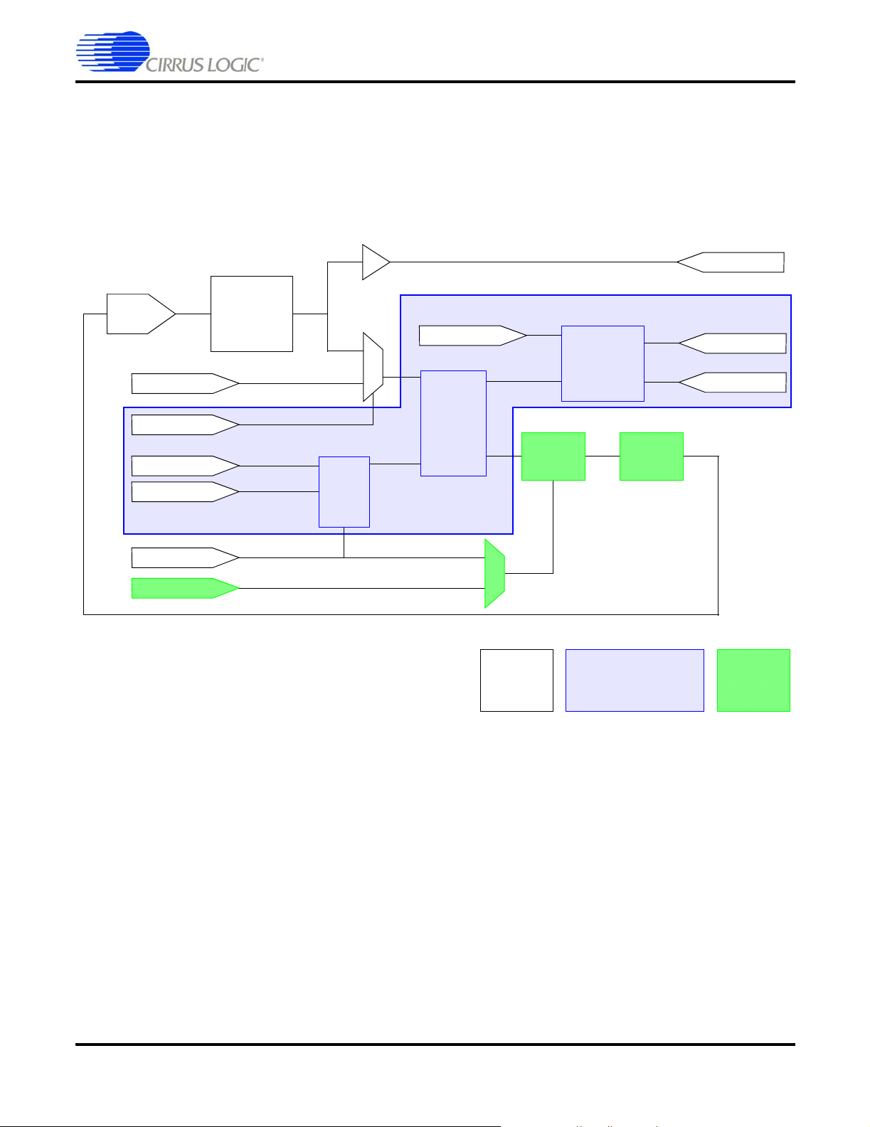
Figure 2 shows a high-level view of the CobraNet CM-2 interface hardware architecture.
Clock
Control
Audio
Serial
Host
Figure 2. CobraNet Interface Hardware Block Diagram
VCXO
CS1810xx/
CS4961xx
Clock
Flash
Memory
Ethernet
Controller
CobraNet CM-2
Module
Ethernet
Magnetics
Flash memory holds the CobraNet firmware and management interface variable settings.
The CS1810xx or CS4961xx network processor is the heart of the CobraNet interface. It
implements the network protocol stacks and performs the synchronous-to-isochronous
and isochronous-to-synchronous conversions. The network processor has a role in
sample clock regeneration and performs all interactions with the host system.
The sample clock is generated by a voltage-controlled crystal oscillator (VCXO)
controlled by the network processor. The VCXO frequency is carefully adjusted to achieve
lock with the network clock.
The Ethernet controller is a standard interface chip that implements the 100-Mbit Fast
Ethernet standard. As per Ethernet requirements the interface is transformer isolated.
8 ©Copyright 2005 Cirrus Logic, Inc. DS651UM23
Version 2.3
Page 9

4.0 Pinout and Signal Descriptions
This section details the chip pinout and signal interfaces for each module and is divided
as follows:
• "CS1810xx & CS4961xx Package Pinouts" on page 10
• "Host Port Signals" on page 12
• "Asynchronous Serial Port (UART Bridge) Signals" on page 12
• "Synchronous Serial (Audio) Signals" on page 13
• "Audio Clock Signals" on page 13
• "Miscellaneous Signals" on page 14
• "Power and Ground Signals" on page 14
• "System Signals" on page 15
CobraNet Hardware User’s Manual
Pinout and Signal Descriptions
DS651UM23 ©Copyright 2005 Cirrus Logic, Inc. 9
Version 2.3
Page 10
CobraNet Hardware User’s Manual
Pinout and Signal Descriptions
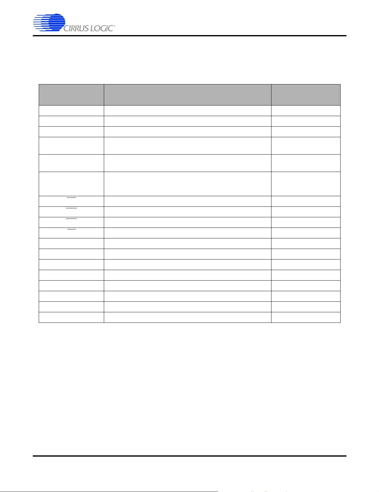
4.1 CS1810xx & CS4961xx Package Pinouts
4.1.1 CS1810xx/CS4961xx Pinout
Ta b l e 1 lists the pinout for the 144-pin LQFP CS1810xx/CS4961xx device. The interfaces
for these signals are expanded in the following sections.
Table 1. CS1810xx/CS4961xx Pin Assignments
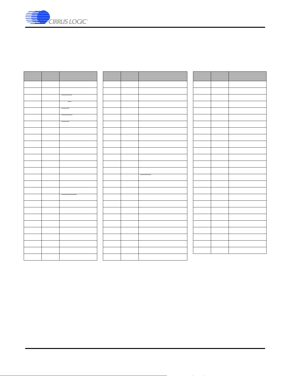
Pin # Pin Name Pin # Pin Name Pin # Pin Name Pin # Pin Name
1 VCXO_CTRL 37 DATA1 73 VDDIO 109 HADDR1
2
3
4
5
6
7
8
9
10
11
12
13
14
15
16
17
18
19
20
21
22
23
24
25
26
27
28
29
30
31
32
33 VDDIO 69 GND 105 HADDR3 141 NC
34
35
36
MCLK_SEL 38 WE 74 ADDR10 110 HADDR0
DBDA 39 DATA0 75 ADDR14 111 HDATA7
DBCK 40 DATA15 76 GND 112 HDATA6
NC 41 DATA14 77 ADDR13 113 VDDIO
NC 42 DATA13 78 NC 114 HDATA5
NC 43 DATA12 79 NC 115 HDATA4
DAO_MCLK 44 VDDIO 80 NC 116 GND
TEST 45 DATA11 81 NC 117 HDATA3
VDDD 46 DATA10 82 ADDR15 118 HDATA2
HS3 47 GND 83 VDDD 119 VDDD
NC 48 DATA9 84 ADDR16 120 HDATA1
GND 49 DATA8 85 ADDR17 121 HDATA0
DAO2_LRCLK 50 NC 86 GND 122 GND
DAO1_DATA3 51 NC 87 ADDR18 123 XTAL_OUT
DAO1_DATA2/HS2 52 NC 88 ADDR19 124 XTO
DAO1_DATA1/HS1 53 NC 89 OE 125 XTI
VDDIO 54 VDDD 90 CS1 126 GND_a
DAO1_DATA0/HS0 55 ADDR12 91 VDDIO 127 FILT2
DAO1_SCLK 56 ADDR11 92 MUTE 128 FILT1
GND 57 GND 93 HRESET 129 VDDA
DAO1_LRCLK 58 ADDR9 94 GND 130 VDDD
UART_TX_OE 59 ADDR8 95 WATCHDOG 131 DAI1_DATA3
VDDD 60 VDDIO 96 IOWAIT 132 DAI1_DATA2
UART_TXD 61 ADDR7 97 REFCLK_IN 133 GND
UART_RXD 62 ADDR6 98 VDDD 134 DAI1_DATA1
GND 63 GND 99 GPIO0 135 DAI1_DATA0
NC 64 ADDR5 100 GPIO1 136 VDDIO
DATA7 65 CS2 101 GND 137 DAI1_SCLK
DATA6 66 VDDD 102 HACK 138 DAI1_LRCLK
DATA5 67 ADDR4 103 HDS 139 GND
DATA4 68 ADDR3 104 HEN 140 HREQ
DATA3 70 ADDR2 106 HADDR2 142 NC
DATA2 71 ADDR1 107 HR/W 143 IRQ1
GND 72 ADDR0 108 GPIO2 144 IRQ2
10 ©Copyright 2005 Cirrus Logic, Inc. DS651UM23
Version 2.3
Page 11
CobraNet Hardware User’s Manual
Pinout and Signal Descriptions
4.1.2 CM-2 Connector Pinout
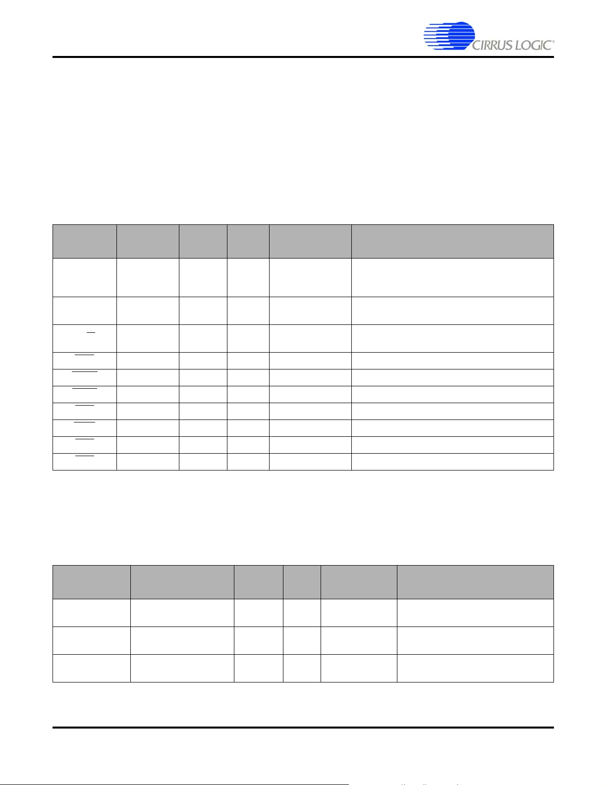
Ta b l e 1 lists the pinout for the four pinout connectors on the CM-2 board (J1-J4). The
interfaces for these signals are expanded following the table.
Table 2. CM-2 Pin Assignments
Conn. Pin # Pin Name Conn. Pin # Pin Name Conn. Pin # Pin Name
J1/J2 A1 UART_RXD J1/J2 B8 GND J3/J4 A15 DAI1_DATA3
J1/J2 A2 UART_TX_OE J1/J2 B9 VCC_+3.3V J3/J4 A16 RSVD3
J1/J2 A3 HACK
J1/J2 A4 HR/W
J1/J2 A5 HDS
J1/J2 A6 HREQ
J1/J2 A7 HEN
J1/J2 A8 HADDR0 J1/J2 B15 VCC_+3.3V J3/J4 B2 VCC_+3.3V
J1/J2 A9 HADDR1 J1/J2 B16 GND J3/J4 B3 GND
J1/J2 A10 HADDR2 J1/J2 B17 VCC_+3.3V J3/J4 B4 VCC_+3.3V
J1/J2 A11 HDATA0 J1/J2 B18 RSVD1 J3/J4 B5 GND
J1/J2 A12 HDATA1 J1/J2 B19 GND J3/J4 B6 VCC_+3.3V
J1/J2 A13 HDATA2 J1/J2 B20 VCC_+3.3V J3/J4 B7 GND
J1/J2 A14 HDATA3 J3/J4 A1 RSVD2 J3/J4 B8 VCC_+3.3V
J1/J2 A15 HDATA4 J3/J4 A2 MUTE
J1/J2 A16 HDATA5 J3/J4 A3 FS1 J3/J4 B10 VCC_+3.3V
J1/J2 A17 HDATA6 J3/J4 A4 MCLK_OUT J3/J4 B11 GND
J1/J2 A18 HRESET
J1/J2 A19 HDATA7 J3/J4 A6 REFCLK_IN J3/J4 B13 GND
J1/J2 A20 HADDR3 J3/J4 A7 DAO1_SCLK/DAI1_SCLK J3/J4 B14 VCC_+3.3V
J1/J2 B1 UART_TXD J3/J4 A8 DAO1_DATA0 J3/J4 B15 GND
J1/J2 B2 GND J3/J4 A9 DAO1_DATA1 J3/J4 B16 GND
J1/J2 B3 VCC_+3.3V J3/J4 A10 DAO1_DATA2 J3/J4 B17 VCC_+5V
J1/J2 B4 GND J3/J4 A11 DAO1_DATA3 J3/J4 B18 VCC_+5V
J1/J2 B5 VCC_+3.3V J3/J4 A12 DAI1_DATA0 J3/J4 B19 AUX_POWER3
J1/J2 B6 GND J3/J4 A13 DAI1_DATA1 J3/J4 B20 AUX_POWER1
J1/J2 B7 VCC_+3.3V J3/J4 A14 DAI1_DATA2
J1/J2 B10 GND J3/J4 A17 WATCHDOG
J1/J2 B11 VCC_+3.3V J3/J4 A18 RSVD4
J1/J2 B12 GND J3/J4 A19 AUX_POWER2
J1/J2 B13 VCC_+3.3V J3/J4 A20 AUX_POWER0
J1/J2 B14 GND J3/J4 B1 GND
J3/J4 B9 GND
J3/J4 A5 MCLK_IN J3/J4 B12 VCC_+3.3V
DS651UM23 ©Copyright 2005 Cirrus Logic, Inc. 11
Version 2.3
Page 12
CobraNet Hardware User’s Manual
Pinout and Signal Descriptions
4.2 Signal Descriptions
4.2.1 Host Port Signals
The host port is used to manage and monitor the CobraNet interface. Electrical operation
and protocol is detailed in the "Host Management Interface (HMI)" on page 23 of this
Manual.
The host port can operate in two modes in order to accomodate Motorola
interfaces. The default mode is Motorola. Intel mode is set via a firmware modification.
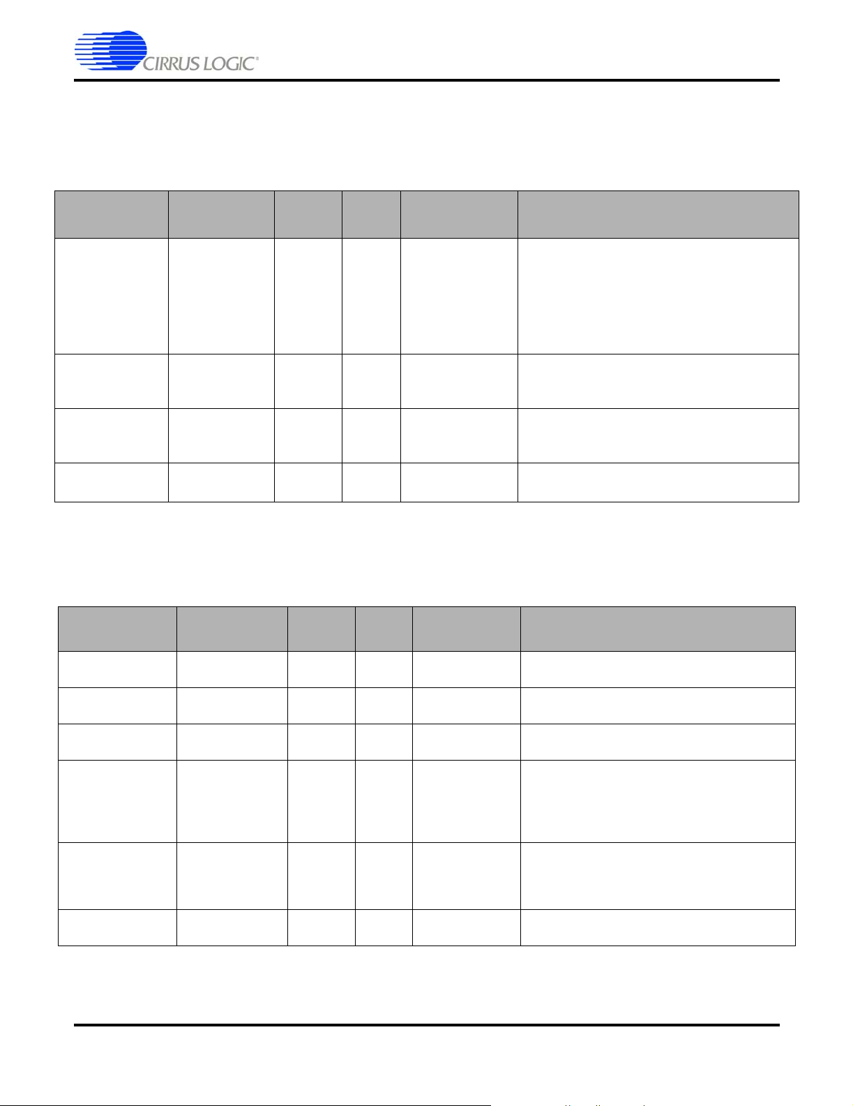
Table 2-1: Host Port Signals
Signal Description Direction
HDATA[7:0] Host Data In/Out
HADDR[3:0] Host Address In
HRW
HRD Host Read In J1:A4 107 Host Read (Intel mode).
Host Request Out J1:A6 140 Host port data request.
HREQ
Host Alert Out J1:A3 102 Host port interrupt request.
HACK
HDS
Host Strobe In J1:A5 103 Host port strobe (Motorola mode).
HWR
Host Enable In J1:A7 104 Host Port Enable.
HEN
Host
Direction
Host Write In J1:A5 103 Host Write (Intel mode).
In J1:A4 107 Host port transfer direction (Motorola mode).
CM-2
Pin #
J1:A19,
A[17:11]
J1:A20,
A[10:8]
CS1810xx/
CS4961xx Pin #
111, 112, 114,
115, 117, 118,
102, 121
105, 106, 109,110 Host port address.
Host port data.
Notes
®
or Intel® style
HCS
Select In J1:A7 104 Select (Intel mode).
4.2.2 Asynchronous Serial Port (UART Bridge) Signals
Level-shifting drive circuits are typically required between these signals and any external
connections.
Signal Description Direction
UART_RXD
UART_TXD
UART_TX_OE Transmit Drive Enable Out J1:A2 23
12 ©Copyright 2005 Cirrus Logic, Inc. DS651UM23
Asynchronous Serial
Receive Data
Asynchronous Serial
Transmit Data
In J1:A1 26 Pull-up to VCC if unused.
Out J1:B1 25
CM-2
Pin #
CS1810xx/
CS4961xx Pin #
Notes
Enable transmit (active high) drive for
two wire multi-drop interface.
Version 2.3
Page 13
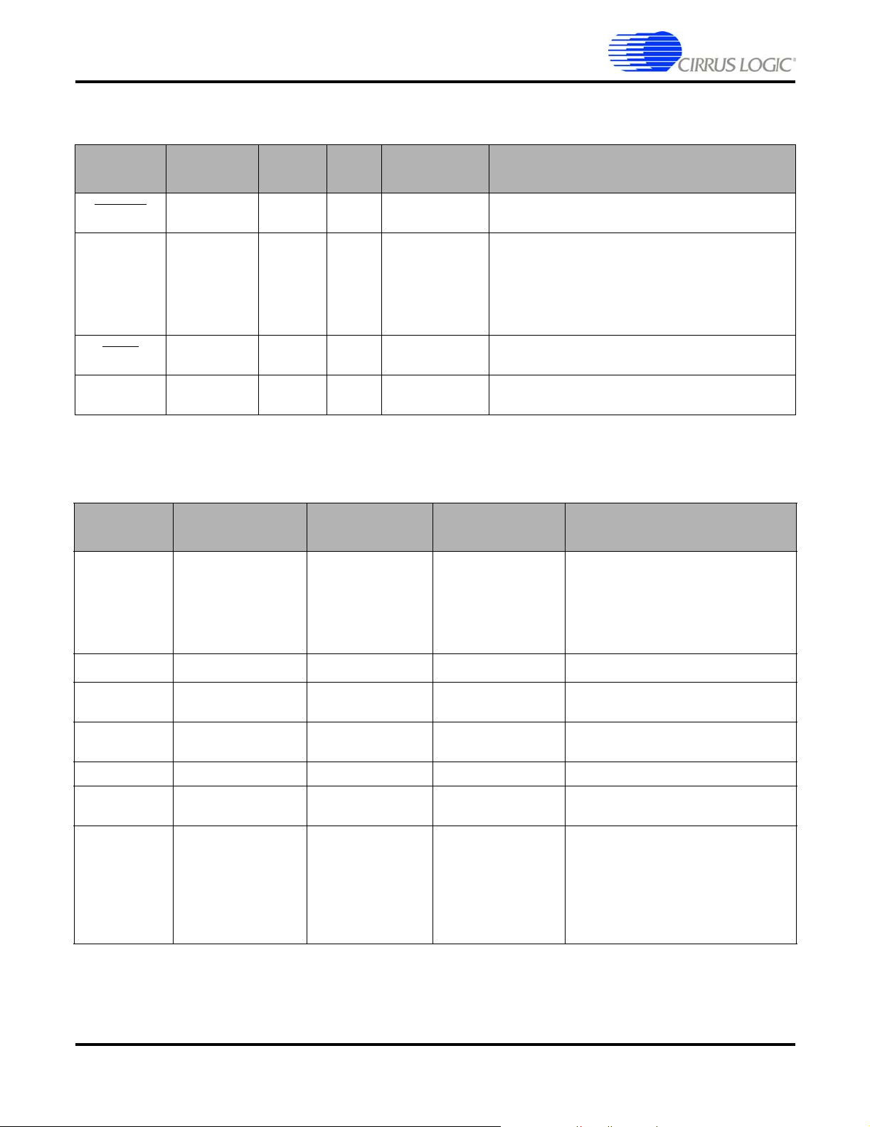
4.2.3 Synchronous Serial (Audio) Signals
The synchronous serial interfaces are used to bring digital audio into and out of the
system. Typically the synchronous serial is wired to ADCs and/or DACs. Detailed timing
and format is described in "Digital Audio Interface" on page 19.
CobraNet Hardware User’s Manual
Pinout and Signal Descriptions
Signal Description Direction
DAO1_SCLK Audio Bit Clock Out J3:A7 20
DAO1_DATA[3:0]
DAI1_DATA[3:0] Audio Input Data In
DAI1_SCLK Audio Bit Clock In J4:A7 137
Audio Output
Data
Out
CM-2
Pin #
J3:A18,
B18
J3:
A[15:12]
CS1810xx/
CS4961xx Pin #
15-17, 19
131, 132, 134, 135
4.2.4 Audio Clock Signals
See "Synchronization" on page 17 for an overview of synchronization modes and issues.
Notes
Synchronous serial bit clock.
64 FS for CS18100x & CS49610x (2x1 channel)
64 FS for CS18101x & CS49611x (2x4
channels)
128 FS for CS18102x & CS49612x (4x4
channels)
Typically tied to DAI1_SCLK.
Output synchronous serial audio data
DAO1_DATA[3:1] not used for CS18100x &
CS49610x.
Input synchronous serial audio data
DAI1_DATA[3:1] not used for CS18100x &
CS49610x.
Should be tied to DAO1_SCLK.
Synchronous serial bit clock.
Signal Description Direction
DAI1_LRCLK
DAO1_LRCLK
(FS1)
DAO2_LRCLK
(FS1)
REFCLK_IN Reference clock In J3:A6 97
MCLK_IN
MCLK_OUT
Sample clock
input
Sample clock
output
Sample clock
output
Master audio
clock input
Master audio
clock output
In 138 Should be tied to DAO1_LRCLK for all devices.
Out J3:A3 22
Out J3:A3 14 FS1 (word clock) for CS18102x & CS49612x.
In J3:A5 8*
Out J3:A4 8* Low jitter 24.576 MHz master audio clock.
CM-2
Pin #
CS1810xx/
CS4961xx Pin #
*An external multiplexor controlled by this pin is required for full MCLK_IN and MCLK out
implementation.
Notes
FS1 (word clock) for CS18100x/CS49610x and
CS18101x/CS49611x.
Clock input for synchronizing network to an
external clock source, for redundancy control
and synchronization of FS divider chain to
external source. See "Synchronization" on
page 17 for more detail.
For systems featuring multiple CobraNet
interfaces operating off a common master
clock. See "Synchronization" on page 17 for
more detail.
DS651UM23 ©Copyright 2005 Cirrus Logic, Inc. 13
Version 2.3
Page 14
CobraNet Hardware User’s Manual
Pinout and Signal Descriptions
4.2.5 Miscellaneous Signals
Signal Description Direction
HRESET Reset In J1:A18 93
WATCHDOG Watch Dog Out J3:A17 95
MUTE
NC No Connect - -
Interface
Ready
Out J3:A2 92
CM-2
Pin #
CS1810xx/
CS4961xx Pin #
28, 50-53, 78-
81, 141, 142
4.2.6 Power and Ground Signals
Signal Description CM-2 Pin #
J1:B20, B17, B15,
B13, B11, B9, B7,
VCC_+3V
System Digital +3.3 v
B5, B3
J3:B14, B12, B10,
B8, B6, B4, B2
System reset (active low).
10 ns max rise time. 1 ms min assertion time.
Toggles at 750 Hz nominal rate to indicate proper
operation. Period duration in excess of 200 ms
indicates hardware or software failure has occurred
and the interface should be reset. Note that
improper operation can also be indicated by short
pulses (<100 ns).
Asserts (active low) during initialization and when a
fault is detected or connection to the network is lost.
CS1810xx/CS4961xx
Pin #
N/A
Notes
Specification
± 0.3v, 500 mA Typ., 750 mA Max.
3.3
_+5V
VCC
VDDD N/A
VDDIO N/A
VDDA N/A 129 Filtered +1.8 V @ 10mA Typ.
AUX_POWER
[3-0]
GND Digital Ground
14 ©Copyright 2005 Cirrus Logic, Inc. DS651UM23
J3;B[18:17] N/A Backwards Compatibility
J3:B[20:19],
A[20:19]
J1:B19, B16, B14,
B12, B10, B8, B6,
B4, B2
J3:B16, B15, B13,
B11, B9, B7, B5,
B3, B1
10, 24, 54, 66, 83,
98, 119, 130
18, 33, 44, 60, 73,
91, 113, 136
N/A
13, 21, 27, 36, 47,
57, 63, 69, 76, 86,
94, 101, 116, 122,
126, 133, 139
+1.8 V @ 500mA Typ. for Core Logic
+3.3 V @ 120mA Typ. for I/O Logic
Version 2.3
Page 15
4.2.7 System Signals
Use these CS1810xx/CS4961xx signals stricktly in the manner described in CM-2
Schematics (Section 9.2 on page 44). Each signal is briefly described below.
CobraNet Hardware User’s Manual
Pinout and Signal Descriptions
Signal Description
VCXO_CTRL A Delta-sigma DAC Output for Controlling the On-board VCXO 1
MCLK_SEL Control Signal for Selecting MCLK Sources 2
DBDA, DBCK I2C Debugger Interface 3, 4
TEST
DATA[15:0] Data Bus for Flash & Ethernet Controller(s)
ADDR[19:0] Address Bus for Flash & Ethernet Controller(s)
WE
CS1
CS2
OE
IOWAIT Wait State Signal from Ethernet Controller(s) 96
GPIO[2:0] General-purpose I/O Signals 99, 100, 108
XTI Reference Clock Input / Crystal Oscillator Input 125
XTO Crystal Oscillator Output 124
Used for testing during manufacturing. Keep grounded for normal
operation.
Write Enable for Flash and Ethernet Controller(s) 38
Chip Select for Flash Memory Device 90
Chip Select for Ethernet Controller(s) 65
Output Enable 89
CS1810xx/CS4961xx
Pin #
9
29-32, 34, 35, 37, 39-43,
45, 46, 48, 49
55, 56, 58, 59, 61, 62, 64,
67, 68, 70-72, 74, 75, 77,
82, 84, 85, 87, 88
XTAL_OUT A Buffered Version of XTI 123
FILT2, FILT1 PLL Loop Filter 127, 128
DAO_MCLK MCLK Input 8
HS[3:0] CS1810xx/CS4961xx Boot Mode Selection 11, 16, 17, 19
DS651UM23 ©Copyright 2005 Cirrus Logic, Inc. 15
Version 2.3
Page 16
CobraNet Hardware User’s Manual
Pinout and Signal Descriptions
4.3 Characteristics and Specifications
4.3.1 Absolute Maximum Ratings
Parameter Symbol Min Max Unit
DC power supplies: Core supply
PLL supply
I/O supply
VDD
VDDA
VDDIO
|VDDA – VDD|
Input current, any pin except supplies I
Input voltage on FILT1, FILT2 V
Input voltage on I/O pins V
Storage temperature T
in
filt
inio
stg
–0.3
–0.3
–0.3
-
-+/- 10mA
-5.0V
–65 150 °C
2.0
2.0
5.0
0.3
2.0 V
Caution: Operation at or beyond these limits may result in permanent damage to the device. Normal operation is
not guaranteed at these extremes.
4.3.2 Recommended Operating Conditions
Parameter Symbol Min Typ Max Unit
DC power supplies: Core supply
PLL supply
I/O supply
|VDDA – VDD|
Ambient operating temperature
- CQ
- DQ
VDD
VDDA
VDDIO
T
A
1.71
1.71
3.13
0
- 40
1.8
1.8
3.3
-
1.89
1.89
3.46
0.3
+ 70
+ 85
V
V
V
V
V
V
V
V
°C
4.3.3 Digital DC Characteristics
(measurements performed under static conditions.)
Parameter Symbol Min Typ Max Unit
High-level input voltage V
Low-level input voltage, except XTI V
Low-level input voltage, XTI V
Input Hysteresis V
High-level output voltage at
I
= –8.0 mAO = –16.0 mA
O
Low-level output voltage at
I
= 8.0 mAO = –16.0 mA
O
V
V
Input leakage current (all pins without internal pull-
IH
IL
ILXTI
hys
OH
OL
I
IN
2.0 - - V
VDDIO * 0.9 - - V
up resistors except XTI)
Input leakage current (pins with internal pull-up
I
IN-PU
resistors, XTI)
4.3.4 Power Supply Characteristics
(measurements performed under operating conditions))
Parameter Min Typ Max Unit
Power supply current:
Core and I/O operating: VDD (Note 1)
PLL operating: VDDA
With external memory and most ports operating: VDDIO
--0.8V
--0.6V
0.3 V
--VDDIO * 0.1V
--5µA
--50µA
-
-
-
500
10
120
-
-
-
mA
mA
mA
NOTES:1. Dependent on application firmware and DSP clock speed.
16 ©Copyright 2005 Cirrus Logic, Inc. DS651UM23
Version 2.3
Page 17
5.0 Synchronization
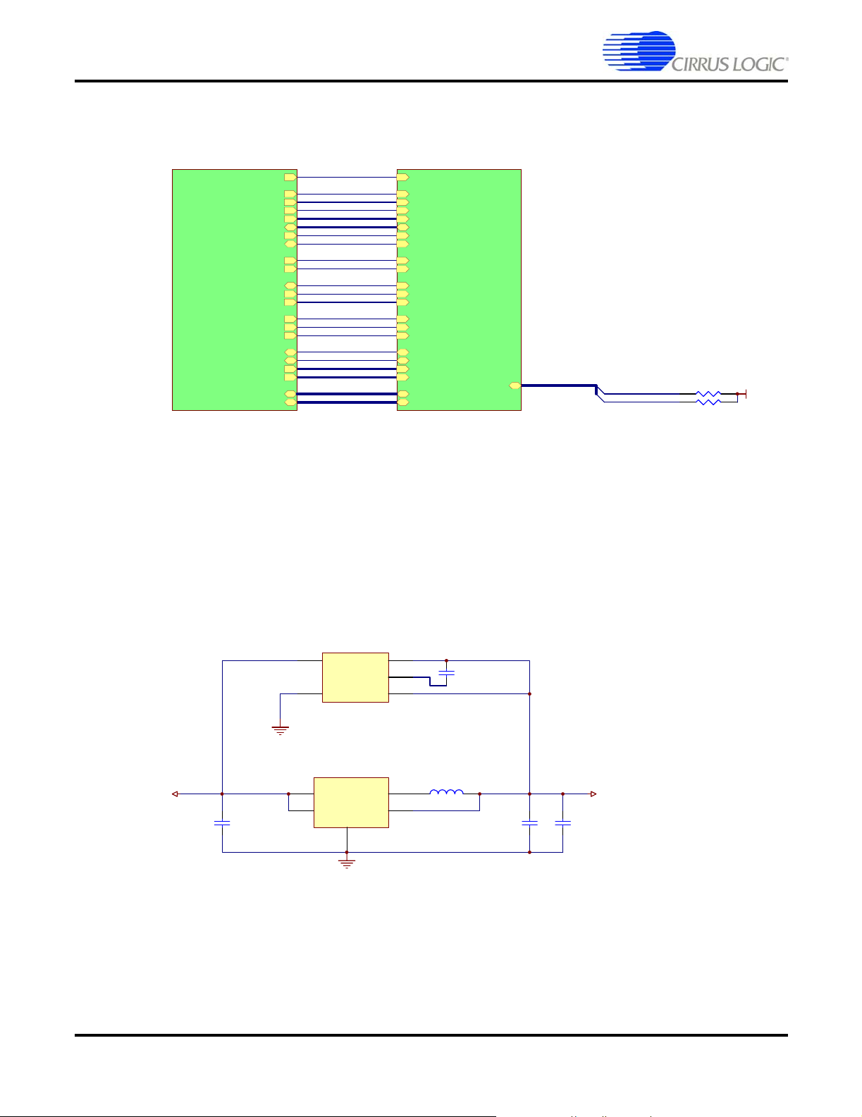
Figure 3 shows clock related circuits for the CS1810xx/CS4961xx and board design
(CM-2). This circuitry allows the synchronization modes documented below to be
achieved. Modes are distinguished by different settings of the multiplexors and software
elements.
CobraNet Hardware User’s Manual
Synchronization
MCLK_OUT
DAC
MCLK_IN
MCLK_SEL
RefClkEnable
RefClkPolarity
REFCLK_IN
BeatReceived
VCXO
24.576 MHz
Edge
Detect
AClkConfig
Sample
Phase
Counter
Legend:
Detector
External
Hardware
Component
(CM2)
Audio
Clock
Generator
Phase
Hardware
Component
(CS1810xx, CS4961xx)
CS1810xx/CS4961xx
FS1
SLCK
Loop
Filter
Internal
Software
Component
Figure 3. Audio Clock Sub-system
5.1 Synchronization Modes
Clock synchronization mode for conductor and performer roles is independently
selectable via management interface variables syncConductorClock and
syncPerformerClock. The role (conductor or performer) is determined by the network
environment including the conductor priority setting of the device and the other devices on
the network. It is possible to ensure you will never assume the conductor role by selecting
a conductor priority of zero. However, it is not reasonable to assume that by setting a high
conductor priority, you will always assume the conductor role. For more information, refer
to CobraNet Programmer’s Reference Manual.
DS651UM23 ©Copyright 2005 Cirrus Logic, Inc. 17
Version 2.3
Page 18

CobraNet Hardware User’s Manual
Synchronization
The following synchronization modes are further described below:
• "Internal Mode" on page 18
• "External Word Clock Mode" on page 18
• "External Master Clock Mode" on page 18
5.1.1 Internal Mode
All CobraNet clocks are derived from the onboard VCXO. The master clock generated by
the VCXO is available to external circuits via the master clock output.
Conductor—The VCXO is “parked” according to the syncClockTrim setting.
Performer—The VCXO is “steered” to match the clock transmitted by the Conductor.
5.1.2 External Word Clock Mode
All CobraNet clocks are derived from the onboard VCXO. The VCXO is steered from an
external clock supplied to the reference clock input. The clock supplied can be any
integral division of the sample clock in the range of 750Hz to 48kHz.
External synchronization lock range: ±5 µs. This specification indicates drift or wander
between the supplied clock and the generated network clock at the conductor. Absolute
phase difference between the supplied reference clock and generated sample clock is
dependant on network topology.
Conductor—This mode gives a means for synchronizing an entire CobraNet network to
an external clock.
Performer—The interface disregards the fine timing information delivered over the
network from the conductor. Coarse timing information from the conductor is still used;
fine timing information is instead supplied by the reference clock. The external clock
source must be synchronous with the network conductor. This mode is useful in
installations where a house sync source is readily available.
5.1.3 External Master Clock Mode
The VCXO is disabled and MCLK_IN is used as the master clock for the node. This is a
“hard” synchronization mode. The supplied clock is used directly by the CobraNet
interface for all timing. This mode is primarily useful for devices with multiple CobraNet
interfaces sharing a common master audio clock. The supplied clock must be
24.576 MHz. The supplied clock must have a ±37 ppm precision.
Conductor—The entire network is synchronized to the supplied master clock.
Performer—The node will initially lock to the network clock and will “jam sync” via the
supplied master clock. The external clock source must be synchronous with the network
conductor.
18 ©Copyright 2005 Cirrus Logic, Inc. DS651UM23
Version 2.3
Page 19

6.0 Digital Audio Interface
p
The CS18101x/CS49611x, CS18102x/CS49612x, and CM-2 support four bi-directional
synchronous serial interfaces. The CS18100x & CS49610x support one bi-directional
synchronous serial interface. All interfaces operate in master mode with DAO1_SCLK as
the bit clock and FS1 as the frame clock. A sample period worth of synchronous serial
data includes two (or four) audio channels. CobraNet supports two synchronous serial bit
rates: 48 Khz and 96 KHz. However, 96 kHz sample rate is not available when using
CS18102x/CS49612x with 16X16 channels. Bit rate is selected by the modeRateControl
variable. All synchronous serial interfaces operate from a common clock at the same bit
rate.
CobraNet Hardware User’s Manual
Digital Audio Interface
DAO1_D A TA0 / D A I1_D A T A0
DAO1_D A TA1 / D A I1_D A T A1
DAO1_D A TA2 / D A I1_D A T A2
DAO1_D A TA3 / D A I1_D A T A3
* Not
Figure 4. Channel Structure for Synchronous Serial Audio at 64FS (One Sample Period) - CS18100x/CS49610x &
resent in CS18100x or CS49610x.
DAO1_DATA0 / DAI1_DATA0
DAO1_DATA1 / DAI1_DATA1
FS1
FS1
1 2
3 4
5 6
7 8
CS18101x/CS49611x
1 2
5 6
3 4
7 8
DAO1_DATA2 / DAI1_DATA2
DAO1_DATA3 / DAI1_DATA3
Figure 5. Channel Structure for Synchronous Serial Audio at 128FS (One Sample Period) - CS18102x/CS49612x
9 10
13 14
11 12
15 16
Default channel ordering is shown above. Note that the first channel always begins after
the rising or falling edge of FS1 (depending on the mode).
DAI1_SCLK period depends on the sample rate selected. Up to 32 significant bits are
received and buffered by the DSP for synchronous inputs. Up to 32 significant bits are
transmitted by the DSP for synchronous outputs. Bit 31 is always the most significant
(sign) bit. A 16-bit audio source must drive to bit periods 31-16 with audio data and bits
15-0 should be actively driven with either a dither signal or zeros. Cirrus Logic
recommends driving unused LS bits to zero.
DS651UM23 ©Copyright 2005 Cirrus Logic, Inc. 19
Version 2.3
Page 20

CobraNet Hardware User’s Manual
Digital Audio Interface
Although data is always transmitted and received with a 32-bit resolution by the
synchronous serial ports, the resolution of the data transferred to/from the Ethernet may
be less. Incoming audio data is truncated to the selected resolution. Unused least
significant bits on outgoing data is zero filled.
6.1 Digital Audio Interface Timing
MCLK_OUT
DAO1_SCLK
FS1
0 –5ns
0 –10ns
Figure 6. Timing Relationship between FS512_OUT, DAO1_SCLK and FS1
An DAO1_SCLK edge follows an MCLK_OUT edge by 0.0 to 5.0ns. An FS1 edge follows
a MCLK_OUT edge by 0.0 to 10.0ns.
Note: The DAO1_SCLK and FS1 might be synchronized with the either the falling edge or
the rising edge of MCLK_OUT. Which edge is impossible to predict since it depends
on power up timing.
≥5ns ≥0ns
DAO1_SCLK
DAI1_DATAx
DAO1_DATAx
0 –12ns
Figure 7. Serial Port Data Timing Overview
Setup times for DAI1_DATAx and FS1 are 5.0 ns with a hold time of 0.0 ns with respect to
the DAI1_SCLK edge. Clock to output times for DAO1_DATAx is 0.0 to 12.0 ns from the
edge of DAO1_SCLK.
20 ©Copyright 2005 Cirrus Logic, Inc. DS651UM23
Version 2.3
Page 21

6.1.1 Normal Mode Data Timing
3
3
3
3
DAI1_SCLK
FS1
CobraNet Hardware User’s Manual
Digital Audio Interface
DAI1_DATAx
DAO1_DATAx
23 22 21 20 19 18 17 16 15 14 13 12 11 10 9 8 7 6 5 4 3 2 231 0 Unused
23 22 21 20 19 18 17 16 15 14 13 12 11 10 9 8 7 6 5 4 3 2 231 0 Unused
Figure 8. Audio Data Timing Detail - Normal Mode, 64FS - CS18100x/CS49610x, CS18101x/CS49611x
DAI1_SCLK
FS1
DAI1_DATAx
DAO1_DATAx
23 22 21 20 19 18 17 16 15 14 13 12 11 10 9 8 7 6 5 4 3 2 231 0 Unused 22 21 20 1918 17 16 15 14 13 12 1110 9 8 7 6 5 4 3 2 2
23 22 21 20 19 18 17 16 15 14 13 12 11 10 9 8 7 6 5 4 3 2 231 0 Unused 22 21 20 19 1817 16 15 14 1312 11 10 9 8 7 6 5 4 3 2 2
Figure 9. Audio Data Timing Detail - Normal Mode, 128FS - CS18102x/CS49612x
Each audio channel is comprised of 32 bits of data, regardless of audio sample size. The
figure above shows 24-bit audio data.
The MSB is left justified and is aligned with FS1. Data is sampled on the rising edge of
DAI_SCLK and data changes on the falling edge.
6.1.2 I2S Mode Data Timing
1 0 Unused
1 0 Unused
DAI1_SCLK
FS1
DAI1_DATAx
DAO1_DATAx
DAI1_SCLK
FS1
DAI1_DATAx
DAO1_DATAx
23 22 21 20 19 18 17 16 15 14 13 12 11 10 9 8 7 6 5 4 3 2 231 0 Unused
23 22 21 20 19 18 17 16 15 14 13 12 11 10 9 8 7 6 5 4 3 2 231 0 Unused
Figure 10. Audio Data Timing Detail - I2S Mode, 64FS - CS18100x/CS49610x, CS18101x/CS49611x
23 22 21 20 19 18 17 16 15 14 13 12 11 10 9 8 7 6 5 4 3 2 231 0 Unused 22 21 20 19 18 17 1615 14 13 12 1110 9 8 7 6 5 4 3 2 2
23 22 21 20 19 18 17 16 15 14 13 12 11 10 9 8 7 6 5 4 3 2 231 0 Unused 22 21 20 1918 17 16 15 14 1312 11 10 9 8 7 6 5 4 3 2 2
2
Figure 11. Audio Data Timing Detail - I
S Mode, 128FS - CS18102x & CS49612x
1 0 Unused
1 0 Unused
Each audio channel is comprised of 32 bits of data, regardless of audio sample size. The
figure above shows 24-bit audio data.
The MSB is left justified and arrives one bit period following FS1. Data is sampled on the
rising edge of DAI_SCLK and data changes on the falling edge.
DS651UM23 ©Copyright 2005 Cirrus Logic, Inc. 21
Version 2.3
Page 22

CobraNet Hardware User’s Manual
3
3
Digital Audio Interface
6.1.3 Standard Mode Data Timing
DAI1_SCLK
FS1
DAI1_DATAx
DAO1_DATAx
23 22 21 20 19 18 17 16 15 14 13 12 11 10 9 8 7 6 5 4 3 2 231 0 Unused
23 22 21 20 19 18 17 16 15 14 13 12 11 10 9 8 7 6 5 4 3 2 231 0 Unused
Figure 12. Audio Data Timing Detail - Standard Mode, 64FS - CS18100x/CS49610x, CS18101x/CS49611x
DAI1_SCLK
FS1
DAI1_DATAx
DAO1_DATAx
23 22 21 20 19 18 17 16 15 14 13 12 11 10 9 8 7 6 5 4 3 2 231 0 Unused 22 21 20 1918 17 16 15 14 13 12 1110 9 8 7 6 5 4 3 2 2
23 22 21 20 19 18 17 16 15 14 13 12 11 10 9 8 7 6 5 4 3 2 231 0 Unused 22 21 20 19 1817 16 15 14 1312 11 10 9 8 7 6 5 4 3 2 2
Figure 13. Audio Data Timing Detail - Standard Mode, 128FS - CS18102x/CS49612x
Each audio channel is comprised of 32 bits of data, regardless of audio sample size. The
figure above shows 24-bit audio data.
The MSB is left justified and is aligned with FS1. Data is sampled on the rising edge of
DAI_SCLK and data changes on the falling edge.
1 0 Unused
1 0 Unused
22 ©Copyright 2005 Cirrus Logic, Inc. DS651UM23
Version 2.3
Page 23

7.0 Host Management Interface (HMI)
7.1 Hardware
The host port is 8 bits wide with 4 bits of addressing. Ten of the 16 addressable registers
are implemented. The upper two registers can be used to configure and retrieve the
status on the host port hardware. However, only the first 8 are essential for normal HMI
communications. It is therefore feasible, in most applications, to utilize only the first 3
address bits and tie the most significant bit (A3) low.
CobraNet Hardware User’s Manual
Host Management Interface (HMI)
Host port hardware supports Intel
®
(little-endian), Motorola®, and Motorola multiplexed
bus (big-endian) protocols. Standard CobraNet firmware configures the port in the
Motorola, big-endian mode.
The host port memory map is shown in Tabl e 3 . Refer also to "HMI Definitions" on
page 33 and "HMI Access Code" on page 34.
Host Address Register
0 Message A (MS)
1 Message B
2 Message C
3 Message D (LS)
4 Data A (MS)
5 Data B
6 Data C
7 Data D (LS)
8 Control
9 Status
Table 3. Host port memory map
The message and data registers provide separate bi-directional data conduits between
the host processor and the CS1810xx/CS4961xx. A 32-bit word of data is transferred to
the CS1810xx/CS4961xx when the host writes the D message or data register after
presumably previously writing the A, B, and C registers with valid data. Data is transferred
from the CS1810xx/CS4961xx following a read of the D message or data register. Again,
presumably the A, B, and C registers are read previously.
Two additional hardware signals are associated with the host port: HACK
and HREQ.
Both are outputs to the host.
HACK
may be wired to an interrupt request input on the host. HACK can be made to
assert (logic 0) on specific events as specified by the hackEnable MI variable. HACK
is
deasserted (logic 1) by issuance of the Acknowledge Interrupt message (see “Messages”
below).
DS651UM23 ©Copyright 2005 Cirrus Logic, Inc. 23
Version 2.3
Page 24

CobraNet Hardware User’s Manual
Host Management Interface (HMI)
HREQ may be wired to a host interrupt or DMA request input. HREQ is used to signal the
host that data is available (read case, logic 0) or space is available in the host port data
channel (write case, logic 1).
The read and write case are distinguished by the HMI based on the preceding message.
Identify, Goto Translation (read), Goto Packet (read) and Goto Counters cause HREQ
represent read status. Goto Translation (write) and Goto Packet (write) switch HREQ
write mode. All other commands have no effect on HREQ
to
to
operation.
In general, the host can read from the CS1810xx/CS4961xx when HREQ
write data to CS1810xx/CS4961xx when HREQ
7.2 Host Port Timing - Motorola® Mode
(CL = 20 pF)
Parameter Symbol Min Max Unit
Address setup before HEN
Address hold time after HEN
Delay between HDS
Data valid after HEN
HEN
and HDS low for read t
Data hold time after HEN
Data high-Z after HEN
HEN
or HDS high to HEN and HDS low for next read t
HEN
or HDS high to HEN and HDS low for next write t
HR/W
rising to HREQ falling
Delay between HDS
Data setup before HEN
HEN
and HDS low for write t
HRW
setup before HEN and HDS low t
HRW
hold time after HEN or HDS high t
Data hold after HEN
HEN
or HDS high to HEN and HDS low with HRW high for
next read
and HDS low t
and HDS low t
Read
then HEN low or HEN then HDS low t
and HDS low with HRW high t
or HDS high after read t
or HDS high after read t
Write
then HEN low or HEN then HDS low t
or HDS high t
or HDS high t
mas
mah
mcdr
mdd
mrpw
mdhr
mdis
mrd
mrdtw
t
mrwirqh
mcdw
mdsu
mwpw
mrwsu
mrwhld
mdhw
t
mwtrd
is low and can
is high.
5-ns
5-ns
0-ns
-19ns
24 - ns
8-ns
-18ns
30 - ns
30 - ns
-12ns
0-ns
8-ns
24 - ns
24 - ns
8-ns
8-ns
30 - ns
or HDS high to HEN and HDS low for next write t
HEN
HRW
rising to HREQ falling
mwd
t
mrwbsyl
30 - ns
-12ns
NOTES:1. The system designer should be aware that the actual maximum speed of the communication port may
be limited by the firmware application. Hardware handshaking on the HREQ
pin/bit should be observed
to prevent overflowing the input data buffer.
24 ©Copyright 2005 Cirrus Logic, Inc. DS651UM23
Version 2.3
Page 25

HADDR[3:0]
HDATA[7:0]
HEN
HRW
HDS
HREQ
t
mas
t
mah
LSP
t
mdhr
t
t
mrwsu
t
mcdr
mdd
t
mrpw
t
mrd
t
mdis
Figure 14. Host Port Read Cycle Timing - Motorola Mode
CobraNet Hardware User’s Manual
Host Management Interface (HMI)
MSP
t
mrwhld
t
mrdtw
t
mrwirqh
HADDR[3:0]
HDATA[7:0]
HEN
HRW
HDS
HREQ
t
mas
t
mah
LSP MSP
t
mdsu
t
mcdw
t
mrwsu
t
mdhw
t
mwpw
t
mwd
t
mrwirql
Figure 15. Host Port Write Cycle Timing - Motorola Mode
t
mrwhld
t
mwtrd
DS651UM23 ©Copyright 2005 Cirrus Logic, Inc. 25
Version 2.3
Page 26

CobraNet Hardware User’s Manual
Host Management Interface (HMI)
7.3 Host Port Timing - Intel® Mode
(CL = 20 pF)
Parameter Symbol Min Max Unit
Address setup before HCS
low
Address hold time after HCS
high
and HRD low or HCS and HWR
and HRD low or HCS and HWR
Read
t
ias
t
iah
5-ns
5-ns
Delay between HRD
Data valid after HCS
HCS
and HRD low for read t
Data hold time after HCS
Data high-Z after HCS
HCS
or HRD high to HCS and HRD low for next read t
HCS
or HRD high to HCS and HWR low for next write t
HRD
rising to HREQ rising
then HCS low or HCS then HRD low t
and HRD low t
or HRD high t
or HRD high t
icdr
idd
irpw
idhr
idis
ird
irdtw
t
irdirqhl
0-ns
-18ns
24 - ns
8-ns
-18ns
30 - ns
30 - ns
-12ns
Write
Delay between HWR
Data setup before HCS
HCS
and HWR low for write t
Data hold after HCS
HCS
or HWR high to HCS and HRD low for next read t
HCS
or HWR high to HCS and HWR low for next write t
HWR
rising to HREQ falling
then HCS low or HCS then HWR low t
or HWR high t
or HWR high t
icdw
idsu
iwpw
idhw
iwtrd
iwd
t
iwrbsyl
0-ns
8-ns
24 - ns
8-ns
30 - ns
30 - ns
-12ns
NOTES:1. The system designer should be aware that the actual maximum speed of the communication port may
be limited by the firmware application. Hardware handshaking on the HREQ
pin/bit should be observed
to prevent overflowing the input data buffer.
26 ©Copyright 2005 Cirrus Logic, Inc. DS651UM23
Version 2.3
Page 27

HADDR[3:0]
HDATA[7:0]
HCS
HWR
HRD
HREQ
t
iah
t
ias
t
icdr
LSP
t
idd
t
irpw
idhr
t
idis
t
ird
t
Figure 16. Parallal Control Port - Intel Mode Read Cycle
CobraNet Hardware User’s Manual
Host Management Interface (HMI)
MSP
t
irdtw
t
irdirq h
HADDR[3:0]
HDATA[7:0]
HCS
HRD
HWR
HREQ
t
iah
t
ias
t
icdw
LSP MSP
t
idhw
t
idsu
t
iwpw
t
iw d
Figure 17. Parallel Control Port - Intel Mode Write Cycle
t
iwrbs yl
t
iwtr d
DS651UM23 ©Copyright 2005 Cirrus Logic, Inc. 27
Version 2.3
Page 28

CobraNet Hardware User’s Manual
Host Management Interface (HMI)
7.4 Protocol and Messages
The message conduit is used to issue commands to the CS1810xx/CS4961xx and
retrieve HMI status. The data conduit is used to transfer data dependent on the HMI state
as determined by commands issued by the host via the message conduit.
7.4.1 Messages
Messages are used to efficiently invoke action in the CS1810xx/CS4961xx. To send a
message, the host optionally writes to the A, B, and C registers. Writing to the D register
transmits the message to the CS1810xx/CS4961xx. A listing of all HMI messages is
shown in Ta bl e 4 . Refer also to "HMI Definitions" on page 33 and "HMI Access Code" on
page 34.
Message
Translate Address n/c Address (MS) Address Address (LS) 0xB3
Acknowledge Interrupt n/c n/c n/c n/c 0xB4
Identify read n/c n/c 7 0xB5
Goto Packet Transmit
Buffer
Goto Translation write n/c n/c 5 0xB5
Acknowledge Packet
Receipt
Transmit Packet n/c n/c n/c 3 0xB5
Goto Counters read n/c n/c 2 0xB5
Goto Packet Receive
Buffer
Goto Translation read n/c n/c 0 0xB5
DRQ Handshake
Mode
write n/c n/c 6 0xB5
n/c n/c n/c 4 0xB5
read n/c n/c 1 0xB5
Table 4. HMI messages
A B C D
28 ©Copyright 2005 Cirrus Logic, Inc. DS651UM23
Version 2.3
Page 29

CobraNet Hardware User’s Manual
Host Management Interface (HMI)
7.4.1.1. Translate Address
Translate Address does not actually update the address pointers but initiates the
processing required to eventually move them. The host can accomplish other tasks,
including HMI Reads and Writes while the address translation is being processed. A
logical description of Translate Address is given below. A contextual use of the Translate
Address operation is shown in the reference implementations. Refer also to "HMI
Definitions" on page 33 and "HMI Access Code" on page 34.
void TranslateAddress(
long address )
{
int msgack = MSG_D;
MSG_A = ( address & 0xff0000 ) >> 16;
MSG_B = ( address & 0xff00 ) >> 8;
MSG_C = address & 0xff;
MSG_D = CVR_TRANSLATE_ADDRESS;
while( !( ( msgack ^ MSG_D ) & ( 1 << MSG_TOGGLE_BO ) ) );
}
7.4.1.2. Interrupt Acknowledge
Causes HACK to be de-asserted.
void InterruptAck( void )
{
int msgack = MSG_D;
MSG_D = CVR_INTERRUPT_ACK;
while( !( ( msgack ^ MSG_D ) & ( 1 << MSG_TOGGLE_BO ) ) );
}
7.4.1.3. Goto Packet
Moves HMI pointers to bridgeRxPktBuffer (write = 0) or bridgeTxPktBuffer (write = 1).
void GotoPacket(
bool write )
{
int msgack = MSG_D;
MSG_C = write ? MOP_GOTO_PACKET_TRANSMIT : MOP_GOTO_PACKET_RECEIVE;
MSG_D = CVR_MULTIPLEX_OP;
while( !( ( msgack ^ MSG_D ) & ( 1 << MSG_TOGGLE_BO ) ) );
}
7.4.1.4. Goto Translation
Moves HMI data pointers to the results of the most recently completed translate address
operation. The write parameter dictates the operation of the HREQ
signal and only needs
to be supplied for applications using hardware data handshaking via this signal.
void GotoTranslation(
bool write = 0 )
{
int msgack = MSG_D;
MSG_C = write ? MOP_GOTO_TRANSLATION_WRITE : MOP_GOTO_TRANSLATION_READ;
MSG_D = CVR_MULTIPLEX_OP;
while( !( ( msgack ^ MSG_D ) & ( 1 << MSG_TOGGLE_BO ) ) );
}
DS651UM23 ©Copyright 2005 Cirrus Logic, Inc. 29
Version 2.3
Page 30

CobraNet Hardware User’s Manual
Host Management Interface (HMI)
7.4.1.5. Packet Received
Sets bridgeRxPkt = bridgeRxReady thus acknowledging receipt of the packet in
bridgeRxPktBuffer.
void PacketReceive( void )
{
int msgack = MSG_D;
MSG_C = MOP_PACKET_RECEIVE;
MSG_D = CVR_MULTIPLEX_OP;
while( !( ( msgack ^ MSG_D ) & ( 1 << MSG_TOGGLE_BO ) ) );
}
7.4.1.6. Packet Transmit
Sets bridgeTxPkt = bridgeTxPktDone+1 thus initiating transmission of the contents of
bridgeTxPktBuffer. Presumably bridgeTxPktBuffer has been previously written with valid
packet data.
void PacketTransmit( void )
{
int msgack = MSG_D;
MSG_C = MOP_PACKET_TRANSMIT;
MSG_D = CVR_MULTIPLEX_OP;
while( !( ( msgack ^ MSG_D ) & ( 1 << MSG_TOGGLE_BO ) ) );
}
7.4.1.7. Goto Counters
Moves HMI data pointers to interrupt status variables (beginning at hackStatus).
void GotoCounters( void )
{
int msgack = MSG_D;
MSG_C = MOP_GOTO_COUNTERS;
MSG_D = CVR_MULTIPLEX_OP;
while( !( ( msgack ^ MSG_D ) & ( 1 << MSG_TOGGLE_BO ) ) );
}
30 ©Copyright 2005 Cirrus Logic, Inc. DS651UM23
Version 2.3
Page 31

7.4.2 Status
CobraNet Hardware User’s Manual
Host Management Interface (HMI)
HMI status can always be retrieved by reading the message conduit. Status is updated in
a pipelined manner whenever the Message D register is read. Reading the message
conduit gives the current status as of the last time the conduit was read. Bitfields in the
HMI Status Register are outlined in Tabl e 5 below. Refer also to "HMI Definitions" on
page 33 and "HMI Access Code" on page 34.
Status Bit(s)
Reserved [31:24]
Region Length [23:8]
Reserved [7:5]
Writable Region 4
Translation Complete 3
Packet Transmission Complete 2
Received Packet Available 1
Message Togglebit 0
Table 5. HMI status bits
DS651UM23 ©Copyright 2005 Cirrus Logic, Inc. 31
Version 2.3
Page 32

CobraNet Hardware User’s Manual
Host Management Interface (HMI)
7.4.3 Data
Before accessing data, address setup must be performed. Address setup consists of
issuing a Translate Address request, waiting for the request to complete, then issuing a
Goto Translation.
Pipelining requires that a “garbage read” be performed following an address change. The
second word read contains the data for the address requested. No similar pipelining issue
exists with respect to write operations.
7.4.3.1. Region length
Distance from the original pointer position (as per Translate Address) to the end of the
instantiated region. A value of 0 indicates an invalid pointer.
7.4.3.2. Writable Region
When set, this bit indicates the address pointer is positioned within a writable region. MI
variables may be modified in a writable region by writing data to the data conduit.
7.4.3.3. Translation Complete
When set, this bit indicates that the address translator is available (translation results are
available and a new translation request may be submitted). This bit is cleared when a
Translate Address message is issued and is set when the translation completes.
7.4.3.4. Packet Transmission Complete
This bit is cleared when transmission is initiated by issuance of the Transmit Packet
message. The bit is set when the packet has been transmitted and the transmit buffer is
ready to accept a new packet.
7.4.3.5. Received Packet Available
This bit is set when a packet is received into the packet bridge. It is cleared when the
packet data is read and receipt is acknowledged by issuance of an Acknowledge Packet
Receipt message. Note that Received Packet Available only goes low when there are no
longer any pending received packets for the packet bridge. The packet bridge has the
capacity to queue multiple packets in the receive direction.
7.4.3.6. Message Togglebit
This bit toggles on completion of processing of each message. A safe means for the host
to acknowledge processing of messages is as follows:
void WaitToggle( void )
{
int msgack = MSG_D; /* clean pipeline */
msgack = MSG_D; /* record current state of togglebit */
MSG_D = YOUR_COMMAND_HERE; /* issue command */
/* wait for togglebit to flip */
while( !( ( msgack ^ MSG_D ) & ( 1 << MSG_TOGGLE_BO ) ) );
}
32 ©Copyright 2005 Cirrus Logic, Inc. DS651UM23
Version 2.3
Page 33

8.0 HMI Reference Code
The following C code provides examples in using HMI messages, HMI status, and the
HMI memory map.
8.1 HMI Definitions
/*========================================================================
** hmi.h
** CobraNet Host Management Interface example code
** Definitions
**------------------------------------------------------------------------
** $Header$
** Copyright (c) 2004, Peak Audio, a division of Cirrus Logic, Inc.
**========================================================================*/
#define MSG_A 0
#define MSG_B 1
#define MSG_C 2
#define MSG_D 3
#define DATA_A 4
#define DATA_B 5
#define DATA_C 6
#define DATA_D 7
#define CONTROL 8
#define STATUS 9
CobraNet Hardware User’s Manual
HMI Reference Code
#define CVR_SET_ADDRESS 0xb2 /* Not availbale on CS1810xx/CS4961xx/CM-2. */
/*CM-1 and Reference Design only. */
#define CVR_TRANSLATE_ADDRESS 0xb3
#define CVR_INTERRUPT_ACK 0xb4
#define CVR_MULTIPLEX_OP 0xb5
#define MOP_GOTO_TRANSLATION_READ 0
#define MOP_GOTO_TRANSLATION_WRITE 5
#define MOP_GOTO_PACKET_RECEIVE 1
#define MOP_GOTO_PACKET_TRANSMIT 6
#define MOP_GOTO_COUNTERS 2
#define MOP_PACKET_TRANSMIT 3
#define MOP_PACKET_RECEIPT 4
#define MOP_IDENTIFY 7
#define MSG_TOGGLE_BO 0
#define MSG_RXPACKET_BO 1
#define MSG_TXPACKET_BO 2
#define MSG_TRANSLATION_BO 3
#define MSG_WRITABLE_BO 4
#define MSG_LENGTH_BO 8
DS651UM23 ©Copyright 2005 Cirrus Logic, Inc. 33
Version 2.3
Page 34

CobraNet Hardware User’s Manual
HMI Reference Code
8.2 HMI Access Code
/*========================================================================
** hmi.c
** CobraNet Host Management Interface example code
** Simple edition
**------------------------------------------------------------------------
** $Header$
** Copyright (c) 2004, Peak Audio, a division of Cirrus Logic, Inc.
**========================================================================*/
#include "hmi.h"
/* variables model HMI state */
long PeekLimit;
long PeekPointer = -1;
long PokeLimit;
long PokePointer = -1;
/* access host port hardware */
#define HMI_BASE 0
unsigned char ReadRegister(
int hmiregister )
{
return *(unsigned char volatile *const) ( hmiregister + HMI_BASE );
}
void WriteRegister(
int hmiregister,
unsigned char value )
{
*(unsigned char volatile *const) ( hmiregister + HMI_BASE ) = value;
}
void SendMessage(
unsigned char message )
{
int msgack = ReadRegister( MSG_D );
/* issue (last byte of) message */
WriteRegister( MSG_D, message );
/* wait for acceptance of message */
while( !( ( msgack ^ ReadRegister( MSG_D ) ) & ( 1 << MSG_TOGGLE_BO ) ) );
}
void SetAddress(
long address )
{
/* translate address */
WriteRegister( MSG_A, ( address & 0xff0000 ) >> 16 );
WriteRegister( MSG_B, ( address & 0xff00 ) >> 8 );
WriteRegister( MSG_C, address & 0xff );
SendMessage( CVR_TRANSLATE_ADDRESS );
/* wait for completion of translate address */
34 ©Copyright 2005 Cirrus Logic, Inc. DS651UM23
Version 2.3
Page 35

CobraNet Hardware User’s Manual
while( !( ReadRegister( MSG_D ) & ( 1 << MSG_TRANSLATION_BO ) ) );
/* goto translation */
WriteRegister( MSG_C, MOP_GOTO_TRANSLATION_READ );
SendMessage( CVR_MULTIPLEX_OP );
/* "garbage" read clears data pipeline */
ReadRegister( DATA_D );
/* maintain local pointers */
PeekPointer = PokePointer = address;
PeekLimit = PokeLimit = PeekPointer +
ReadRegister( MSG_C ) + ( ReadRegister( MSG_B ) << 8 );
/* read-only region addressed */
if( !( ReadRegister( MSG_A ) & ( 1 << MSG_WRITABLE_BO ) ) ) {
PokeLimit = PokePointer;
}
}
unsigned long Peek(
long address )
{
if( address != PeekPointer ) {
SetAddress( address );
}
if( PeekPointer >= PeekLimit ) {
throw "Peek addressing error!";
}
unsigned long value = ReadRegister( DATA_A ) << 24;
value += ReadRegister( DATA_B ) << 16;
value += ReadRegister( DATA_C ) << 8;
value += ReadRegister( DATA_D );
PeekPointer++; /* maintain local pointer */
return value;
}
HMI Reference Code
void Poke(
long address,
unsigned long value )
{
if( address != PokePointer ) {
SetAddress( address );
}
if( PokePointer >= PokeLimit ) {
throw "Poke addressing error or read-only!";
}
WriteRegister( DATA_A, (unsigned char) ( ( value >> 24 ) & 0xff ) );
WriteRegister( DATA_B, (unsigned char) ( ( value >> 16 ) & 0xff ) );
WriteRegister( DATA_C, (unsigned char) ( ( value >> 8 ) & 0xff ) );
WriteRegister( DATA_D, (unsigned char) ( value & 0xff ) );
/* maintain local pointers */
PokePointer++;
PeekPointer = -1; /* force SetAddress()next Peek() to freshen data */
}
DS651UM23 ©Copyright 2005 Cirrus Logic, Inc. 35
Version 2.3
Page 36

CobraNet Hardware User’s Manual
HMI Reference Code
8.3 CM-1, CM-2 Auto-detection
The following function is useful for systems that support both the CM-1 and CM-2 or
where a CobraNet interface is an optional add-in.
Detect() returns 0 if no CobraNet interface module is detected, 1 for CM-1 and 2 for CM-2.
int Detect( void ) {
/* check for presence of CM-1 */
MSG_B = 0x55; /* write to CM-1 CVR register */
DATA_A = 0xaa; /* write to unused CM-1 register to flip data bus */
if( MSG_B == 0x55 ) { /* read back CVR */
/* redo same detection with different data */
MSG_B = 0x3c;
DATA_A = 0xc3;
if( MSG_B == 0x3c ) {
return 1; /* CM-1 detected */
}
}
/* check for presence of CM-2 */
/* issue identify command */
MSG_C = MOP_IDENTIFY;
MSG_D = CVR_MULTIPLEX_OP;
int msgack = MSG_D; /* clean pipeline */
msgack = MSG_D;
/* wait for togglebit to flip in response to command */
int tm0 = gettimeofday();
while( !( ( MSG_D ^ toggle ) & ( 1 << MSG_TOGGLE_BO ) ) ) {
int tm1 = gettimeofday();
if( ( tm1 - tm0 ) > time_out ) {
return 0; /* command timed out, no CobraNet interface present */
}
}
int garbage = MSG_D; /* clean pipeline */
/* verify identify results */
if( DATA_A == 'C' ) if( DATA_B == 'S' )
if( DATA_C == ( 18101 >> 8 ) ) if( DATA_D == ( 18101&0xff ) {
return 2; /* CM-2 detected */
}
return 0; /* no interface or non-supported interface */
}
36 ©Copyright 2005 Cirrus Logic, Inc. DS651UM23
Version 2.3
Page 37

9.0 Mechanical Drawings and Schematics
The section contains detailed drawings of the CM-2 board and CS1810xx/CS4961xx
device package design. The mechanical drawings are arranged as follows:
• "CM-2 Module Assembly Drawing, Top" on page 38
• "General PCB Dimensions" on page 40
• "Example Configuration, Side View" on page 41
• "Faceplate Dimensions" on page 42
• "Connector Detail" on page 43
• "CM-2 RevF Schematic Page 1 of 7" on page 44
• "CM-2 RevF Schematic Page 2 of 7" on page 45
• "CM-2 RevF Schematic Page 3 of 7" on page 46
• "CM-2 RevF Schematic Page 4 of 7" on page 47
• "CM-2 RevF Schematic Page 5 of 7" on page 48
• "CM-2 RevF Schematic Page 6 of 7" on page 49
CobraNet Hardware User’s Manual
Mechanical Drawings and Schematics
• "CM-2 RevF Schematic Page 7 of 7" on page 50
• "144-Pin LQFP Package Drawing" on page 51
DS651UM23 ©Copyright 2005 Cirrus Logic, Inc. 37
Version 2.3
Page 38

CobraNet Hardware User’s Manual
Mechanical Drawings and Schematics
9.1 CM-2 Mechanical Drawings
NOT TO SCALE
Figure 18. CM-2 Module Assembly Drawing, Top
38 ©Copyright 2005 Cirrus Logic, Inc. DS651UM23
Version 2.3
Page 39

CobraNet Hardware User’s Manual
Mechanical Drawings and Schematics
NOT TO SCALE
Figure 19. CM-2 Module Assembly Drawing, Bottom
DS651UM23 ©Copyright 2005 Cirrus Logic, Inc. 39
Version 2.3
Page 40

CobraNet Hardware User’s Manual
Mechanical Drawings and Schematics
3.500
0.175
2x Mounting holes for PCB standoffs
4x 0.16 Hole, 0.3 pads
B20
A20
B1B1
A1A1
Component Side = J3
Bottom Side = J4
Viewed from component side up.
B20
A20
0.175
Component Side = J1
Bottom Side = J2
3.500
2.86
0.3
General PCB dimensions
NOT TO SCALE
2x Mounting holes for front faceplate.
Figure 20. General PCB Dimensions
40 ©Copyright 2005 Cirrus Logic, Inc. DS651UM23
Version 2.3
Page 41

CobraNet Hardware User’s Manual
Mechanical Drawings and Schematics
0.340
This distance accounts for the thickness of the faceplate
NOT TO SCALE
Figure 21. Example Configuration, Side View
DS651UM23 ©Copyright 2005 Cirrus Logic, Inc. 41
Version 2.3
Page 42

CobraNet Hardware User’s Manual
Mechanical Drawings and Schematics
0.862
4-40 PEM's, x2
0.680
0.300
1.000
0.810
0.800
0.700
1.000 max, 0.9 typ.
0.490
0.340
0.175
ote: Mechanical dimensions for the CM-2 and CM-1 Rev F are identical.
There are differences with earlier versions of the CM-1, however. For
3.500
0.550
Faceplate material is 20 guage, 0.037" thick
1.343
Chrome plating on faceplate
1.333
Faceplate Dimensions
reference, earlier versions of the CM-1 dimensions are shown in RED.
0.175
0.125 dia, 2x
0.431
0.421
0.300
2x, Hole Diameter 0.160
NOT TO SCALE
0.500
Figure 22. Faceplate Dimensions
42 ©Copyright 2005 Cirrus Logic, Inc. DS651UM23
Version 2.3
Page 43

CobraNet Hardware User’s Manual
Mechanical Drawings and Schematics
Component
Side Up
8x 0.047 Alignment holes
J3
J1
0.157 1.576 1.925 3.343
0.208
0.039
Connector Detail
Figure 23. Connector Detail
DS651UM23 ©Copyright 2005 Cirrus Logic, Inc. 43
Version 2.3
NOT TO SCALE
Page 44
CobraNet Hardware User’s Manual
Mechanical Drawings and Schematics
9.2 CM-2 Schematics
connector
connector.sch
HRESET#
HEN#
HRW
HDS#
HADDR[0..3]
HDATA[0..7]
HREQ#
HACK#
WATCHDOG
MUTE#
UART_TX_OE
UART_TXD
UART_RXD
MCLK_OUT
MCLK_IN
REFCLK_IN
SSI_CLK
SSI_DIN[0..3]
SSI_DOUT[0..3]
RSVD[1..5]
AUX_POWER[0..3]
FS1
HRESET#
HEN#
HRW
HDS#
HADDR[0..3]
HDATA[0..7]
HREQ#
HACK#
WATCHDOG
MUTE#
UART_TX_OE
UART_TXD
UART_RXD
MCLK_OUT
MCLK_IN
REFCLK_IN
FS1
SSI_CLK
SSI_DIN[0..3]
SSI_DOUT[0..3]
RSVD[1..5]
AUX_POWER[0..3]
core
core.sch
HRESET#
HEN#
HRW
HDS#
HADDR[0..3]
HDATA[0..7]
HREQ#
HACK#
WATCHDOG
MUTE#
UART_TX_OE
UART_TXD
UART_RXD
MCLK_OUT
MCLK_IN
REFCLK_IN
FS1
SSI_CLK
SSI_DIN[0..3]
SSI_DOUT[0..3]
RSVD[1..5]
AUX_POWER[3..0]
GPIO[0..1]
GPIO[0..1]
GPIO[0..1] is not used elsewhere.
These pulldowns ar e used for test points and
to keep these signa ls at valid levels.
GPIO1
R1GP IO0
R2
10K Ohm
GND
VCC_+3.3
This linear regulator is used to assure that the +1.8v rail quickly passes
the 0.5v threshold at powerup, thus minimizing power sequencing issues
and making sure that the DSP does not draw excessive power as the
power rails ramp up. This linear regulator is set with Vout=1.22v, so it
is effectively shut off once the switching regulator comes up. Further
testing and characterization of the DSP is require to determine if this
linear regulator is in fact required.
U9
1
IN
2
GND
LTC1761
U1
LTC3406-1.8
4
VIN
1
RUN
Vout/FB
C1
10 uF, X5R, 6.3 Volts
This is a simple switching regulator. It produces
1.8V at >500 mA at about 90% efficency. A simple low drop
out linear regulator would be a cheaper alternative at the
expense of power. A linear regulator would dissapate
about 0.75 watts max, This switching regulator dissapates
about 0.10 watts max.
GND
2
OUT
BYP
ADJ
4
3
5
3
SW
5
L1
2.2 uH
C45
0.01 uF
C2
10 uF, X5R, 6.3 Volts
VCC_+1.8
C3
Figure 24. CM-2 RevF Schematic Page 1 of 7
44 ©Copyright 2005 Cirrus Logic, Inc. DS651UM23
Version 2.3
Page 45

CobraNet Hardware User’s Manual
Mechanical Drawings and Schematics
LED_BUF[0..7]
LED_BUF0
LED_BUF1
LED_BUF2
LED_BUF3
LED_BUF4
LED_BUF5
LED_BUF6
LED_BUF7
VCC_+3.3
RN2
VCC_+3.3
12
3456789
MCLK_SEL
VCXO_CTRL
WATCHDOG
GND
GND
10K Ohm
10K Ohm, 8x Array
10
3.3K Ohm
R3
R15
IOWAIT
MUTE#
C16
0.1 uF
C17
0.1 uF
C18
0.1 uF
C20
0.1 uF
R4
R6
R8
R10
30.9 Ohm, 1%R530.9 Ohm, 1%
30.9 Ohm, 1%R730.9 Ohm, 1%
30.9 Ohm, 1%R930.9 Ohm, 1%
R11
30.9 Ohm, 1%
30.9 Ohm, 1%
LED Filters go close to the connector.
9
7
15
U2
Q11Q22Q33Q44Q55Q66Q7
Q0
VCC
16
VCC_+3.3
C15
VCC_+3.3
SCLR#10SCK11RCK12OE#13DIN
0.1 uF
VCC_+3.3
LED_CTRL0
LED_CTRL[0..2]
74LV595
CASCADE
GND
8
14
GND
LED_CTRL1
LED_CTRL2
MCLK_OUT
AUX_POWER[3..0]
LED_CTRL[0..2]
LED_BUF[0..7]
LED_BUF[0..7]
CLK_25
AUX_POWER[3..0]
CLK_25
AUX_POWER[0..3]
ADDR[0..19]
DATA[0..15]
HRESET_BUF#
OE#
WE#
MAC_CS#
IOWAIT
macphy1
macphy1.sch
6
U10B
74LVC32
4
5
GND
HRESET#
HRESET#
HRESET_BUF#
MAC_CS#
OE#
WE#
IOWAIT
ADDR[0..19]
DATA[0..15]
OE#
WE#
IOWAIT
MAC_CS#
DATA[0..15]
ADDR[0..19]
HRESET_BUF#
HRW
HDS#
HEN#
HREQ#
HACK#
HADDR[0..3]
HDATA[0..7]
dsp
dsp.sch
CLK_25
CLK_25
LED_BUF[0..7]
LED_CTRL[0..2]
MAC_IRQ0
MAC_IRQ0
MAC_IRQ0
UART_TX_OE
UART_RXD
UART_TXD
AUX_POWER[0..3]
DATA[0..15]
ADDR[0..19]
HRESET_BUF#
OE#
WE#
ADDR[0..19]
DATA[0..15]
HRESET_BUF#
OE#
WE#
MAC_CS#
IOWAIT
macphy2
macphy2.sch
MAC_IRQ1
FS1
SSI_CLK
SSI_DOUT[0..3]
SSI_DIN[0..3]
GPIO[0..1]
REFCLK_IN
WATCHDOG
MUTE#
FLASH_CS#
MAC_IRQ1 LED_BUF[0..7]
flash
flash.sch
ADDR[0..19]
DATA[0..15]
FLASH_CS#
MAC_IRQ1
FLASH_CS#
MCLK_INTERNAL
MCLK_SEL
VCXO_CTRL
CLK_25
RSVD[1..5]
VCC_+3.3
VCC_+3.3
16
B4
CD4
VCC
VCCA4VCC
CTRLB1GND
CTRLA1CTRLC1CTRLD1GNDC2GND
U3
MCLK_INTERNAL
24.9 Ohm, 1%
R44
4
VCC
A/B11A21B
G
15
GND
MCLK_IN
MCLK_SEL
AB3
AB2
C19
0.1 uF
MCLK_OUT
R16
7
1Y
2Y
2A52B
11
GND
VCXO_OUT
MCLK_IN
CD3
OUT
OUT
D2
24.9 Ohm, 1%
9
3Y
3
14
GND
VCXO_OUT
24.576 MHz VCXO
12
GND
4Y
3B103A
4B134A
6
GND
GND
VCXO_OUT
VCC_+3.3
C22
0.1 uF
VCC_+3.3
U4
74LVC157
8
C21
0.1 uF
HEN#
HEN#
HRW
HDS#
HADDR[0..3]
HDATA[0..7]
HREQ#
HACK#
UART_TX_OE
UART_TXD
UART_RXD
FS1
SSI_CLK
SSI_DIN[0..3]
SSI_DOUT[0..3]
HREQ#
FS1
HACK#
SSI_CLK
UART_RXD
UART_TXD
SSI_DIN[0..3]
UART_TX_OE
SSI_DOUT[0..3]
HRW
HDS#
HADDR[0..3]
HDATA[0..7]
RSVD[1..5]
GPIO[0..1]
GPIO[0..1]
VCXO_CTRL
MCLK_SEL
REFCLK_IN
MCLK_INTERNAL
WATCHDOG
MUTE#
REFCLK_IN
WATCHDOG
CLK_25
MUTE#
RSVD[1..5]
3.3K Ohm
R12
VCXO_CTRL
Figure 25. CM-2 RevF Schematic Page 2 of 7
DS651UM23 ©Copyright 2005 Cirrus Logic, Inc. 45
Version 2.3
Page 46

CobraNet Hardware User’s Manual
Mechanical Drawings and Schematics
ADDR0
DATA[0..15]
DATA[0..15]
DATA7
DATA6
DATA5
DATA4
DATA3
DATA2
DATA1
DATA0
OE#
WE#
FLASH_CS#
OE#
WE#
FLASH_CS#
VCC_+3.3
VCC_+3.3
GND
45
U5
D13
D14
D15/A-1
ADDR[0..19]
NC/A19
9
ADDR19
VCC
NC/A1816A17
17
48
ADDR17
ADDR18
37
VCC_+3.3
30
32
42
44
D8
D9
D6
D7
D10
D11
D12
A151A142A133A124A115A106A97A8
A16
ADDR11
ADDR12
ADDR13
ADDR14
ADDR15
ADDR16
38
40
D5
8
ADDR9
ADDR10
29
31
33
35
D0
D1
D2
D3
D4
A718A619A520A421A322A223A124A0
ADDR4
ADDR5
ADDR6
ADDR7
ADDR8
34
36
39
41
43
13
47
BYTE#
NC/VPP
ADDR2
ADDR3
15
14
NC/WP#
NC/RY/BY#
12
25
ADDR1
HRESET_BUF#
11
26
28
FLASH_TSOP
CE#
OE#
WE#
GND
46
GND
27
NC
RESET#
10
HRESET_BUF#
C23
0.1 uF
VCC_+3.3
ADDR[0..19]
Figure 26. CM-2 RevF Schematic Page 3 of 7
46 ©Copyright 2005 Cirrus Logic, Inc. DS651UM23
Version 2.3
Page 47

CobraNet Hardware User’s Manual
Mechanical Drawings and Schematics
FS1
These pullups and pulldowns are used
to set the boot mode of the DSP. The
appropriate resistor is installed to select
the boot mode.
RSVD1
HS3 - Down
SSI_DOUT2
HS2 - Down
SSI_DOUT0
SSI_DOUT1
HS0 - Down
HS1 - Up
3.3K Ohm
R51
R49
R47
R43
FS1
RSVD[1..5]
C53
74LVC157
8
0.1 uF
VCC_+3.3
HADDR[0..3]
SSI_CLK
GPIO[0..1]
HDATA[0..7]
SSI_DOUT[0..3]
SSI_CLK
SSI_DIN[0..3]
GPIO[0..1]
R53
4
7
9
12
U11
GND
VCC
1Y
2Y
3Y
A/B11A21B
G
GND
2A52B
3
11
14
GND
GND
GND
4Y
3B103A
4B134A
6
GND
GND
GND
16
VCC_+3.3
15
3.3K Ohm
R50
R48
R46
R42
VCC_+3.3
Default Boot Mode:
D1
U10C
1N4148W
8
9
GND
C52
74LVC32
10
45
6
2
8
VCC_+1.8
R56
0.1 uF
3.3K Ohm
VCC_+3.3
CN4
0.1 uF, 4x Array
24.9 Ohm, 1%
DAO1_LRCLK
DAO2_LRCLK
R57
10K Ohm
123
4
JP1
CON4
Debug Port
GND
VCC_+3.3
DEBUG_CLK
DEBUG_DATA
R14
R13
3.3K Ohm
CN5
0.1 uF, 4x Array
45
3
6
3
2
7
1
VCC_+3.3
7
1
8
HRW
HDS#
HRW
HDS#
103
107
U6
HDS#
HR/W#
TEST
9
GND
DBDA
3
DBCK
4
VDDIO
73
VDDIO
136
VDDIO
113
VDDIO
91
VDDIO
60
VDDIO
44
VDDIO
33
VDDIO
18
VDDD
130
VDDD
119
VDDD
98
VDDD
83
VDDD
66
VDDD
VCC_+1.8 VCC_+3.3
54
VDDD
24
VDDD
10
RESET#
93
HRESET_BUF#
HRESET_BUF#
HEN#
HACK#
HACK#
HEN#
102
104
HEN#
HACK#
EXT_WE#
EXT_OE#89EXT_CS1#
38
OE#
WE#
OE#
WE#
HREQ#
HREQ#
140
HREQ#
EXT_CS2#
65
90
FLASH_CS#
MAC_CS#
MAC_CS#
FLASH_CS#
HADDR0
HADDR1
HADDR2
HADDR3
105
106
109
110
HADDR3
HADDR2
HADDR1
IOWAIT
SD_D15/EXT_D740SD_D14/EXT_D641SD_D13/EXT_D542SD_D12/EXT_D443SD_D11/EXT_D345SD_D10/EXT_D246SD_D9/EXT_D148SD_D8/EXT_D0
96
IOWAIT
DATA14
DATA15
HADDR[0..3]
HADDR0
DATA13
HDATA4
HDATA5
HDATA6
HDATA7
111
112
114
115
HDATA7
HDATA6
HDATA5
HDATA4
DATA9
DATA10
DATA11
DATA12
HDATA[0..7]
HDATA0
HDATA1
HDATA2
HDATA3
117
118
120
121
HDATA3
HDATA2
HDATA1
HDATA0
SD_D7/EXT_D1529SD_D6/EXT_D1430SD_D5/EXT_D1331SD_D4/EXT_D1232SD_D3/EXT_D1134SD_D2/EXT_D1035SD_D1/EXT_D937SD_D0/EXT_D8
49
DATA4
DATA5
DATA6
DATA7
DATA8
MCLK_INTERNAL
MCLK_INTERNAL
8
DAO_MCLK
DATA3
R54
DAO1_LRCLK
SSI_CLK_J
SSI_DOUT1
SSI_DOUT2
SSI_DOUT3
20
22
15
17
DAO1_SCLK
DAO1_LRCLK
DAO1_DATA3
DAO1_DATA2/HS216DAO1_DATA1/HS1
EXT_A1887EXT_A19
88
39
DATA0
DATA1
DATA2
ADDR18
ADDR19
SSI_DOUT[0..3]
SSI_DOUT0
19
DAO1_DATA0/HS0
85
ADDR16
ADDR17
EXT_A1684EXT_A17
DAO2_LRCLK
12
14
DAO2_LRCLK
EXT_A15
75
82
ADDR14
ADDR15
RSVD5
NC
77
ADDR13
RSVD4
NC5NC6NC
SD_A13/EXT_A14
ADDR12
RSVD2
7
SD_A12/EXT_A1155SD_A11/EXT_A10
56
ADDR11
RSVD[1..5]
RSVD1
11
HS3
SD_A10/EXT_A1274SD_A14/EXT_A13
ADDR9
ADDR10
SD_A9/EXT_A958SD_A8/EXT_A8
DAO1_LRCLK
138
DAI1_LRCLK
59
ADDR8
SSI_CLK_J
137
DAI1_SCLK
SD_A7/EXT_A761SD_A6/EXT_A6
ADDR7
SSI_DIN3
131
DAI1_DATA3
62
ADDR6
SSI_DIN2
132
DAI1_DATA2
SD_A5/EXT_A5
64
ADDR5
SSI_DIN1
134
DAI1_DATA1
SD_A4/EXT_A467SD_A3/EXT_A3
ADDR4
SSI_DIN0
135
DAI1_DATA0
68
ADDR3
SSI_DIN[0..3]
SD_A2/EXT_A270SD_A1/EXT_A171SD_A0/EXT_A0
ADDR2
141NC142
NC
ADDR1
RSVD3
72
ADDR0
RSVD[1..5]
MUTE#
MCLK_SEL
MAC_IRQ0
MAC_IRQ1
REFCLK_IN
WATCHDOG
GPIO0
GPIO1
REFCLK_IN
WATCHDOG
MUTE#
MAC_IRQ0
MAC_IRQ1
MCLK_SEL
143
144
95
100
108
92
2
97
IRQ1
IRQ2
GPIO099GPIO1
GPIO2
MUTE#
MCLK_SEL
REFCLK_IN
WATCHDOG_OUT
UART_TX_OE
UART_TXD25UART_RXD
XTAL_OUT
XTI
XTO
FILT2
23
26
123
125
124
127
UART_TXD
UART_RXD
UART_TX_OE
UART_RXD
UART_TXD
UART_TX_OE
VCC_+1.8
C44
0.1 uF
VCXO_CTRL
VCXO_CTRL
1
VCXO_CTRL
FILT1
128
VDD_A
GND_A
NC
NC
NC
NC
NC
NC
NC
NC
NC
GND
GND
GND
GND
GND
GND
GND
GND
GND
GND
GND
GND
GND
GND
GND
GND
CS18101
C5
10 uF, X5R, 6.3 Volts
FB1
FBEAD, 68 Ohm @ 100 MHz
C24
0.1 uF
C4
10 uF, X5R, 6.3 Volts
VCC_DSPA
129
126
81
80
79
78
53
52
51
50
28
139
133
122
116
101
94
86
76
69
63
57
47
36
27
21
13
C43
1000 pF, COG
R41
5.90K Ohm
C42
C41
22 pF
2.2 uF, X7R, 1206
CN3
CN2
45
6
2
8
VCC_+1.8
CN1
45
6
2
8
VCC_+1.8
0.1 uF, 4x Array
0.1 uF, 4x Array
3
7
1
3
7
1
45
6
2
8
VCC_+3.3
CN12
45
6
2
8
VCC_+3.3
0.1 uF, 4x Array
0.1 uF, 4x Array
DATA[0..15]
3
7
1
3
7
1
IOWAIT
DATA[0..15]
ADDR[0..19]
24.9 Ohm, 1%
Y1
25 MHz
R45
CLK_25
ADDR[0..19]
CLK_25
1 MegOhm
R55
1 2
C40
22 pF
Figure 27. CM-2 RevF Schematic Page 4 of 7
DS651UM23 ©Copyright 2005 Cirrus Logic, Inc. 47
Version 2.3
Page 48

CobraNet Hardware User’s Manual
ih
Mechanical Drawings and Schematics
LED_BUF[0..7]
LED_BUF[0..7]
R19
49.9 Ohm, 1%
LED_CTRL[0..2]
CN8
0.1 uF, 4x Array
45
3
FB2
FBEAD, 68 Ohm @ 100 MHz
VCC_+3.3 VCC_PHY1
6
2
8
C7
10 uF, X5R, 6.3 Volts
CN7
0.1 uF, 4x Array
45
6
C46
0.01 uF
C6
2
8
VCC_+3.3
10 uF, X5R, 6.3 Volts
45
6
2
8
VCC_+3.3 VCC_PHY1
CN6
0.1 uF, 4x Array
LED_CTRL[0..2]
7
1
3
7
1
3
7
1
LED_BUF1
LED_BUF0
LED_BUF3
LED_BUF2
T1B
VCC_PHY1
GNDVCC_PHY1
C26
LED_CTRL0
LED_CTRL1
LED_CTRL2
VCC_+3.3
GND
VCC_PHY1VCC_+3.3
L1
L2
L3
L4
17
18TXD+
TXD+
789
C27
GND
0.1 uF
R20
49.9 Ohm, 1%
U7
68
69
70
71
60
61
62
16
17
18
19
48
35
28
27
90
73
72
55
36
20
5
1234567
16
TXD-
TXD-
0.1 uF
33
GPIO0
GPIO1
GPIO2
GPIO3
SPEED#
DUP#
LINKACT#
TEST1
TEST2
TEST3
TEST4
TEST5
AVDD
AVDD
AVDD
DVDD
DVDD
DVDD
DVDD
DVDD
DVDD
DVDD
RST
14
80
100
HRESET_BUF#
MAC_IRQ0
S1
RXD+
34
TXO-
TXO+
WAKEUP79PW_RST#
INT
SHIELD
SHIELD
S2
8
14
15
RXD+
101112 13
C28
GND
30
29
RXI-
RXI+
IOR#1IOW#2AEN3IOWAIT
4
WE#
IOWAIT
MAC_CS#
AUX_POWER0
AUX_POWER1
AUX_POWER2
AUX_POWER3
FB3
FB4
FB5
FB6
J5
RJ45
RXD- RXD-
H2006A
0.1 uF
R17R18
49.9 Ohm, 1%
45
47
41
46
RXD038RXD139RXD240RXD3
RX_ER
RX_DV
RX_CLK
IO1691CMD92SA493SA594SA695SA796SA897SA9
98
ADDR2
ADDR3
ADDR1
ADDR4
VCC_+3.3
ADDR0
FBEAD, 68 Ohm @ 100 MHz
R32
R31
R30
R29
R28
R27
C25
0.1 uF
49
TXD050TXD151TXD252TXD3
TX_CLK
SD06SD17SD28SD39SD410SD511SD612SD7
VCC_+3.3
DATA0
DATA1
DATA2
AUX_POWER[0..3]
AUX_POWER[0..3]
Note: See Text Warning
75 Ohm, 1%
C48
75 Ohm, 1%
78
43
53
44
54
CRS
COL
TX_EN
LINK_O
13
89
DATA3
DATA4
DATA5
DATA6
DATA7
DATA8
Warning: Failure to properly install and
configure the aux. Ethernet signals can result in
very bad things (i.e., fire, smoke, bad hair days).
If power is supplied via the RJ-45 connector then
only the ferrite beads are installed (not the
resistors). If power is not supplied via the RJ-45
then the resistors are installed and the beads are
DM9000
EECS
EECK
EEDO
EEDI
BGGND
BGRES
CLK20MO
X1_25M
X2_25M
NC
NC
NC
AGND
AGND
DGND
DGND
DGND
DGND
DGND
DGND
DGND
DGND
not.
GND
GND
12
RN7
67
66
65
64
R25
25
26
59
22
CLK_25
21
77
75
74
32
31
99
81
76
63
58
42
23
15
3456789
Keep res close to chip pins.
6.8K Ohm, 1%
CLK_25
3.3K Ohm, 8x Array
10
C51
0.1 uF
VCC_+3.3
VCC
14
GND
7
VCC_+3.3
U10E
74LVC32
0.01 uF, 2KV
SHIELD
57
24
56
37
SD
MDC
MDIO
LINK_I
SD1582SD1483SD1384SD1285SD1186SD1087SD988SD8
DATA9
DATA10
DATA11
DATA12
DATA13
DATA14
DATA15
3
U10A
74LVC32
1
2
OE#
MAC_CS#
OE#
MAC_CS#
WE#
MAC_IRQ0
HRESET_BUF#
ADDR[0..19]
IOWAIT
ADDR[0..19]
DATA[0..15]
DATA[0..15]
Figure 28. CM-2 RevF Schematic Page 5 of 7
48 ©Copyright 2005 Cirrus Logic, Inc. DS651UM23
Version 2.3
Page 49

CobraNet Hardware User’s Manual
Mechanical Drawings and Schematics
SHIELD
SHIELD
S1
S2
AUX_POWER0
AUX_POWER1
AUX_POWER2
LED_BUF5
L1
L2
LED_BUF4
L3
LED_BUF7
L4
LED_BUF6
1234567
8
LED_BUF[0..7]
LED_BUF[0..7]
R23
20
21
TXD+
TXD+
T1A
4
5
VCC_PHY2OE#
C31
0.1 uF
GND
C30
0.1 uF
R24
VCC_PHY2 GND
49.9 Ohm, 1%
49.9 Ohm, 1%
23
24
TXD-
RXD+
TXD-
RXD+
123
6 19
C32
GND
AUX_POWER3
FB8
FB9
FB10
FB11
J6
RJ45
FBEAD, 68 Ohm @ 100 MHz
R38
R37
R36
R35
R34
R33
22
RXD- RXD-
H2006A
0.1 uF
49.9 Ohm, 1%
R22
C29
R21
AUX_POWER[0..3]
AUX_POWER[0..3]
Note: See Text Warning
75 Ohm, 1%
C49
75 Ohm, 1%
0.1 uF
VCC_+3.3
Warning: Failure to properly install and
configure the aux. Ethernet signals can result in
very bad things (i.e., fire, smoke, bad hair days).
If power is supplied via the RJ-45 connector then
only the ferrite beads are installed (not the
resistors). If power is not supplied via the RJ-45
then the resistors are installed and the beads are
0.01 uF, 2KV
SHIELD
not.
12
RN8
GND
3456789
GND
3.3K Ohm, 8x Array
10
FB7
FBEAD, 68 Ohm @ 100 MHz
VCC_+3.3 VCC_PHY2
R52
3.3K Ohm
CN11
0.1 uF, 4x Array
45
3
6
2
7
1
8
C9
10 uF, X5R, 6.3 Volts
CN10
0.1 uF, 4x Array
45
3
6
2
C47
0.01 uF
VCC_+3.3
C8
10 uF, X5R, 6.3 Volts
VCC_+3.3 VCC_PHY2
8
CN9
0.1 uF, 4x Array
45
6
2
8
7
1
3
7
1
U10D
12
MAC_CS#
68
69
70
71
60
61
62
16
17
VCC_+3.3
18
19
48
GND
35
28
27
VCC_PHY2VCC_+3.3
90
73
72
55
36
20
5
11
74LVC32
13
34
29
30
33
U8
GPIO0
GPIO1
GPIO2
GPIO3
DUP#
TEST1
TEST2
TEST3
TEST4
TEST5
AVDD
AVDD
AVDD
DVDD
DVDD
DVDD
DVDD
DVDD
DVDD
DVDD
RST
14
SPEED#
80
HRESET_BUF#
HRESET_BUF#
TXO+
LINKACT#
INT
100
MAC_IRQ1
MAC_IRQ1
RXI-
RXI+
TXO-
IOR#1IOW#2AEN3IOWAIT
WAKEUP79PW_RST#
WE#
MAC_CS#
WE#
47
RXD038RXD139RXD240RXD3
RX_CLK
IO1691CMD92SA493SA594SA695SA796SA897SA9
4
ADDR0
ADDR2
ADDR3
IOWAIT
IOWAIT
41
ADDR1
45
RX_DV
ADDR4
46
RX_ER
98
VCC_+3.3
ADDR[0..19]
ADDR[0..19]
49
TXD050TXD151TXD252TXD3
TX_CLK
SD06SD17SD28SD39SD410SD511SD612SD7
VCC_+3.3
DATA0
37
54
78
53
DATA1
DATA2
DATA3
DATA4
57
43
44
24
56
SD
CRS
COL
LINK_I
TX_EN
LINK_O
13
89
DATA5
DATA6
DATA7
DATA8
DATA9
DATA10
DM9000
MDC
EECS
MDIO
67
EECK
66
EEDO
65
EEDI
64
BGGND
BGRES
CLK20MO
X1_25M
X2_25M
NC
NC
NC
AGND
AGND
DGND
DGND
DGND
DGND
DGND
DGND
DGND
DGND
SD1582SD1483SD1384SD1285SD1186SD1087SD988SD8
DATA11
DATA12
DATA13
DATA14
DATA15
DATA[0..15]
DATA[0..15]
R26
CLK_25
Keep res close to chip pins.
6.8K Ohm, 1%
The secondary Ethernet MAC and connector are optional.
If it is not required then all parts on this page can be depopulated
(or removed entirely from a new design based on this circuit).
CLK_25
25
26
59
22
21
77
75
74
32
31
99
81
76
63
58
42
23
15
OE#
MAC_CS#
Figure 29. CM-2 RevF Schematic Page 6 of 7
DS651UM23 ©Copyright 2005 Cirrus Logic, Inc. 49
Version 2.3
Page 50

CobraNet Hardware User’s Manual
Mechanical Drawings and Schematics
GND
GND
GND
12
GND
12
12
GND
GND
VCC_+3.3
VCC_+3.3
12
RN3
3456789
SSI_DIN2
SSI_DIN3
Note: Pull-ups/downs on SSI_DOUT[0..4] are located on the DSP schematic page.
GND
VCC_+3.3
B1B2B3B4B5B6B7B8B9
J2
A1A2A3A4A5A6A7A8A9
HRW
HACK#
UART_RXD UART_TXD
UART_TX_OE
10K Ohm, 8x Array
RN4
10
SSI_DOUT3
RSVD4
RSVD5
SSI_DIN0
SSI_DIN1
RSVD3
SSI_CLK
GND
GND
VCC_+3.3
VCC_+3.3
HEN#
HREQ#
HDS#
HADDR0
GND
HADDR1
VCC_+3.3
B10
A10
HADDR2
GND
GND
GND
GND
VCC_+3.3
VCC_+3.3
VCC_+3.3
B11
B12
B13
B14
B15
B16
A11
A12
A13
A14
A15
A16
HDATA0
HDATA1
HDATA2
HDATA3
HDATA4
HDATA5
3456789
RSVD2
FS1
MCLK_IN
HADDR3
RSVD1
GND
VCC_+3.3
B17
B18
B19
B20
A17
A18
A19
A20
HRESET#
HADDR3
HDATA6
HDATA7
10K Ohm, 8x Array
RN5
10
HDATA3
HDATA5
HDATA6
HDATA7
VCC_+3.3
J4
CNM_CONN40
3456789
10
HADDR0
HADDR1
HADDR2
HDATA0
HDATA1
HDATA2
HDATA4
GND
GND
GND
GND
VCC_+3.3
VCC_+3.3
VCC_+3.3
B1B2B3B4B5B6B7B8B9
A1A2A3A4A5A6A7A8A9
RSVD2
SSI_CLK
SSI_DOUT0
FS1
MCLK_OUT
MCLK_IN
REFCLK_IN
MUTE#
10K Ohm, 8x Array
VCC_+3.3
SSI_DOUT1
RN6
HEN#
GND
GND
GND
VCC_+3.3
VCC_+3.3
VCC_+3.3
B10
B11
B12
B13
B14
A10
A11
A12
A13
A14
SSI_DOUT2
SSI_DOUT3
SSI_DIN0
SSI_DIN1
SSI_DIN2
3456789
HDS#
HACK#
HREQ#
UART_TXD
GND
GND
VCC_+5
B15
B16
B17
B18
A15
A16
A17
A18
RSVD4
SSI_DIN3
WATCHDOG
10K Ohm, 8x Array
10
UART_TX_OE
UART_RXD
REFCLK_IN
These pullups/downs are used to assure a valid logic level if a signal is
tri-stated or not connected. In some situations, these may not be required.
C39
0.1 uF
VCC_+5
C38
0.1 uF
C37
0.1 uF
C36
0.1 uF
AC Signal Return Path Caps
VCC_+5
B19
B20
CNM_CONN40
A19
A20
AUX_POWER0 AUX_POWER1
AUX_POWER2 AUX_POWER3
C35
0.1 uF
C34
0.1 uF
C33
0.1 uF
VCC_+3.3
Note: Similar AC signal return path caps must be included on the motherboard near the connector.
C14
10 uF, X5R, 6.3 Volts
C13
10 uF, X5R, 6.3 Volts
C12
10 uF, X5R, 6.3 Volts
Power Decoupling Caps
C11
10 uF, X5R, 6.3 Volts
C10
VCC_+3.3
10 uF, X5R, 6.3 Volts
GND
VCC_+3.3
B1B2B3B4B5B6B7B8B9
J1
A1A2A3A4A5A6A7A8A9
HACK#
HRW
UART_RXD UART_TXD
UART_TX_OE
HRESET#
HEN#
HRW
HREQ#
HACK#
HDS#
HRW
HDS#
HACK#
HREQ#
HRESET#
GND
HEN#
HDS#
HDATA[0..7]
VCC_+3.3
HDATA[0..7]
GND
HREQ#
HDATA0
HEN#
HDATA1
GND
VCC_+3.3
HADDR0
HDATA2
VCC_+3.3
B10
A10
HADDR2
HADDR1
HDATA3
HDATA4
RSVD1
GND
GND
GND
GND
GND
GND
GND
GND
VCC_+3.3
VCC_+3.3
VCC_+3.3
VCC_+3.3
VCC_+3.3
B11
B12
B13
B14
B15
B16
B17
B18
B19
B20
A11
A12
A13
A14
A15
A16
A17
A18
A19
A20
HDATA1
HDATA2
HDATA3
HDATA4
HDATA5
HDATA6
HDATA7
HRESET#
HDATA0
HADDR3
CNM_CONN40
GND
VCC_+3.3
B1B2B3B4B5B6B7B8B9
J3
A1A2A3A4A5A6A7A8A9
FS1
MUTE#
RSVD2
MCLK_OUT
VCC_+3.3
MCLK_IN
GND
GND
GND
GND
VCC_+3.3
SSI_CLK
REFCLK_IN
GND
VCC_+3.3
VCC_+3.3
VCC_+3.3
VCC_+3.3
VCC_+5
VCC_+5
B10
B11
B12
B13
B14
B15
B16
B17
B18
B19
B20
CNM_CONN40
A10
A11
A12
A13
A14
A15
A16
A17
A18
A19
A20
SSI_DOUT0
WATCHDOG
SSI_DOUT1
SSI_DOUT2
SSI_DOUT3
SSI_DIN0
SSI_DIN1
SSI_DIN2
SSI_DIN3
AUX_POWER0 AUX_POWER1
AUX_POWER2 AUX_POWER3
RSVD3 RSVD3
RSVD4
These two mounting holes are located at the
"back" of the CM-2, near the main interface
These two mounting holes are located near
the front panel of the CM-2.
connectors.
Place near the Ethernet connectors.
R40
1
M3
MOUNTING
M1
WATCHDOG
RSVD1
RSVD2
RSVD3
WATCHDOG
RSVD4
MUTE#
RSVD5
RSVD[1..5]
MUTE#
RSVD[1..5]
SSI_DOUT0
SSI_DOUT1
HADDR[0..3]
HADDR0
HADDR[0..3]
HADDR1
HADDR2
HADDR3
SSI_DOUT[0..3]
SSI_DOUT2
SSI_DOUT[0..3]
HDATA5
HDATA6
HDATA7
SSI_CLK
SSI_DOUT3
SSI_DIN0
SSI_DIN1
SSI_DIN2
SSI_DIN3
FS1
MCLK_OUT
MCLK_IN
REFCLK_IN
UART_RXD
UART_TXD
UART_TX_OE
AUX_POWER0
AUX_POWER1
AUX_POWER2
AUX_POWER3
SSI_DIN[0..3]
SSI_CLK
MCLK_IN
MCLK_OUT
SSI_DIN[0..3]
AUX_POWER[0..3]
FS1
UART_TXD
UART_RXD
REFCLK_IN
UART_TX_OE
AUX_POWER[0..3]
MOUNTING
M4
MOUNTING
1
M2
MOUNTING
0 Ohm
1
R39
0 Ohm
1
SHIELD
C50
0.01 uF, 2KV
Figure 30. CM-2 RevF Schematic Page 7 of 7
50 ©Copyright 2005 Cirrus Logic, Inc. DS651UM23
Version 2.3
Page 51

9.3 CS1810xx/CS4961xx Package
D
D1
CobraNet Hardware User’s Manual
Mechanical Drawings and Schematics
E
E1
Notes:
1. Controlling dimension is millimeter.
2. Dimensioning and tolerancing per ASME
Y14.5M-1994.
DIM
A --- --- 1.60 --- --- .063”
A1 0.05 --- 0.15 .002” --- .006”
b 0.17 0.22 0.27 .007” .009” .011”
D 22.00 BSC .866”
D1 20.00 BSC .787”
E 22.00 BSC .866”
E1 20.00 BSC .787”
e 0.50 BSC .020”
θ
L 0.45 0.60 0.75 .018” .024” .030”
L1 1.00 REF .039” REF
ddd 0.08 .003”
e
b
ddd
M
B
SEATING PLANE
L1
θ
L
Figure 31. 144-Pin LQFP Package Drawing
MILLIMETERS INCHES
MIN NOM MAX MIN NOM MAX
0° --- 7° 0° --- 7°
TOLERANCES OF FORM AND POSITION
B
A
A1
DS651UM23 ©Copyright 2005 Cirrus Logic, Inc. 51
Version 2.3
Page 52

CobraNet Hardware User’s Manual
Mechanical Drawings and Schematics
9.4 Temperature Specifications
• Thermal Coefficient (junction-to-ambient): θja - 38° C / Watt
• Ambient Temperature Range: 0-70 deg C
• Junction Temperature Range: 0-125 deg C
52 ©Copyright 2005 Cirrus Logic, Inc. DS651UM23
Version 2.3
Page 53

10.0 Ordering Information
10.1 Device Part Numbers
CS181002-CQ/A1 2x2 Channels 0°C to +70°C 144-pin LQFP
CS181012-CQ/A1 8x8 Channels 0°C to +70°C 144-pin LQFP
CS181022-CQ/A1 16x16 Channels 0°C to +70°C 144-pin LQFP
CS181002-CQZ/A1 2x2 Channels 0 °C to +70°C 144-pin LQFP Lead Free
CS181012-CQZ/A1 8x8 Channels 0 °C to +70°C 144-pin LQFP Lead Free
CS181022-CQZ/A1 16x16 Channels 0 °C to +70°C 144-pin LQFP Lead Free
CS496102-CQZ/A1 2x2 Channels + DSP 0 °C to +70°C 144-pin LQFP Lead Free
CS496112-CQZ/A1 8x8 Channels + DSP 0 °C to +70°C 144-pin LQFP Lead Free
CS496122-CQZ/A1 16x16 Channels + DSP 0 °C to +70°C 144-pin LQFP Lead Free
10.2 Device Part Numbering Scheme
CobraNet Hardware User’s Manual
Ordering Information
CS1810x 2 — CQZ/A1
Base Part Number
Channel Count Designator:
0 = 2x2
1 = 8x8
2 = 16x16
ROM Version
(ROM ID)
CS4961x 2 — CQZ/A1
Base Part Number
Channel Count Designator:
0 = 2x2
1 = 8x8
2 = 16x16
ROM Version
(ROM ID)
Die Revision
Lead-free Designator:
Z = Lead-free Device Packaging
(not present if device contains lead)
Package Type:
Q = LQFP (144-pin)
Temperature Grade Designator:
C = Commercial (0°C to +70 °C)
Die Revision
Lead-free Designator:
Z = Lead-free Device Packaging
(not present if device contains lead)
Package Type:
Q = LQFP (144-pin)
Temperature Grade Designator:
C = Commercial (0°C to +70 °C)
Note: Go to the Cirrus Logic Internet site at http://www.cirrus.com to find contact information for your local sales representative.
Figure 32. Device Part Numbering Explanation
DS651UM23 ©Copyright 2005 Cirrus Logic, Inc. 53
Version 2.3
Page 54

CobraNet Hardware User’s Manual
n
t
e
.
r
,
-
n
,
E
-
E
N
,
R
,
'
e
Ordering Information
Contacting Cirrus Logic Support
For all product questions and inquiries contact a Cirrus Logic Sales Representative.
o find the one nearest to you go to www.cirrus.com
IMPORTANT NOTICE
irrus Logic, Inc. and its subsidiaries ("Cirrus") believe that the information contained in this document is accurate and reliable. However, the informatio
s subject to change without notice and is provided "AS IS" without warranty of any kind (express or implied). Customers are advised to obtain the lates
ersion of relevant information to verify, before placing orders, that information being relied on is current and complete. All products are sold subject to th
erms and conditions of sale supplied at the time of order acknowledgment, including those pertaining to warranty, indemnification, and limitation of liability
o responsibility is assumed by Cirrus for the use of this information, including use of this information as the basis for manufacture or sale of any items, o
or infringement of patents or other rights of third parties. This document is the property of Cirrus and by furnishing this information, Cirrus grants no license
xpress or implied under any patents, mask work rights, copyrights, trademarks, trade secrets or other intellectual property rights. Cirrus owns the copy
ights associated with the information contained herein and gives consent for copies to be made of the information only for use within your organizatio
ith respect to Cirrus integrated circuits or other products of Cirrus. This consent does not extend to other copying such as copying for general distribution
dvertising or promotional purposes, or for creating any work for resale.
ERTAIN APPLICATIONS USING SEMICONDUCTOR PRODUCTS MAY INVOLVE POTENTIAL RISKS OF DEATH, PERSONAL INJURY, OR SEVER
PROPERTY OR ENVIRONMENTAL DAMAGE ("CRITICAL APPLICATIONS"). CIRRUS PRODUCTS ARE NOT DESIGNED, AUTHORIZED OR WAR
RANTED FOR USE IN AIRCRAFT SYSTEMS, MILITARY APPLICATIONS, PRODUCTS SURGICALLY IMPLANTED INTO THE BODY, AUTOMOTIV
AFETY OR SECURITY DEVICES, LIFE SUPPORT PRODUCTS OR OTHER CRITICAL APPLICATIONS. INCLUSION OF CIRRUS PRODUCTS I
UCH APPLICATIONS IS UNDERSTOOD TO BE FULLY AT THE CUSTOMER'S RISK AND CIRRUS DISCLAIMS AND MAKES NO WARRANTY, EX
PRESS, STATUTORY OR IMPLIED, INCLUDING THE IMPLIED WARRANTIES OF MERCHANTABILITY AND FITNESS FOR PARTICULAR PURPOSE
ITH REGARD TO ANY CIRRUS PRODUCT THAT IS USED IN SUCH A MANNER. IF THE CUSTOMER OR CUSTOMER'S CUSTOMER USES O
PERMITS THE USE OF CIRRUS PRODUCTS IN CRITICAL APPLICATIONS, CUSTOMER AGREES, BY SUCH USE, TO FULLY INDEMNIFY CIRRUS
ITS OFFICERS, DIRECTORS, EMPLOYEES, DISTRIBUTORS AND OTHER AGENTS FROM ANY AND ALL LIABILITY, INCLUDING ATTORNEYS
FEES AND COSTS, THAT MAY RESULT FROM OR ARISE IN CONNECTION WITH THESE USES.
irrus Logic, Cirrus, and the Cirrus Logic logo designs are trademarks of Cirrus Logic, Inc. All other brand and product names in this document may b
rademarks or service marks of their respective owners.
otorola is a registered trademark of Motorola, Inc.
Intel is a registered trademark of Intel, Inc.
54 ©Copyright 2005 Cirrus Logic, Inc. DS651UM23
Version 2.3
 Loading...