

Page 1
Dimmable LED Driver IC
LED +
LED -
C
OUT
NTC
C
BST
D
BST
Q
BUCK
CS1680
VAC
BUCKGD
BSTOUT
9
CLAMP
BUCKZCD
BUCKSENSE
eOTP
12
2
13
R
CLAMP
R
S
C
NTC
R
BST
D1
12VAC/VDC
D2
V
rec t
V
BST
D
BUCK
Q
CLAMP
C5
VDD
GPIO
BST SENSE
BSTGD
C
rect
6
7
3
11
15
R
BUCK(Sense)
R
BST(Sense)
Q
BST
R4
Z2
D3
D4
GND
1
CTRL1
16
R
CTRL1
R1
C4
R
CTRL2
CTRL2
4
5
14
Q1
Z1
R5
C1 C3
R3
U1
D5
D6
R
rect
C2
Q2
L
BST
L
BUCK
R2
for Low-voltage Lighting
CS1680
Features
• Best-in-class Transformer Compatibility
- Magnetic Transformers
- Electronic Transformers
• Best-in-class Dimmer Compatibility
- Leading-edge (TRIAC) Dimmers
- Trailing-edge Dimmers
• High Efficiency
- Up to 80% for CS1680-00 Applications
- Up to 83% for CS1680-02 Applications
• Flicker-free Dimming
• 5% Minimum Dimming Level
• Cascade Boost-buck Topology with Constant-current
Output
- CS1680-00 Output Voltage 15V
- CS1680-02 Output Voltage 21V
• Fast Startup
• Tight LED Current Regulation: Better than ±10%
• >0.9 Power Factor on Magnetic Transformers
• Soft Start
• Protections:
- Output Open/Short
- Boost Overvoltage
- Overcurrent Detection
- External Overtemperature Using NTC
Overview
The CS1680 is a cascade boost-buck dimmable LED
driver for the 12V halogen lamp-replacement market.
The CS1680 uses a Cirrus Logic proprietary intelligent
digital control that provides exceptional single-lamp and
multi-lamp transformer compatibility for non-dimmer systems and dimmer systems paired with electronic and
magnetic low-voltage transformers.
The CS1680 integrates a continuous conduction mode
(CCM) boost converter that provides transformer compatibility and dimmer compatibility. An adaptive digital
algorithm controls the boost stage and dimmer compatibility operation mode to enable flicker-free operation
down to 5% output current with leading-edge and trailing-edge dimmers.
Applications
• MR16 Lamps
• All 12VAC/VDC Low-voltage Lighting Applications
Ordering Information
See page 15.
Cirrus Logic, Inc.
http://www.cirrus.com
Copyright Cirrus Logic, Inc. 2014
(All Rights Reserved)
OCT’14
DS1055F1
Page 2
1. INTRODUCTION
V
Z
POR
+
-
Voltage
Regulator
6
VDD
13
BUCKSENSE
+
-
9
BUCKZCD
+
-
12
BUCKGD
VAC
DAC
+
-
ZCD
4
GND
15
BSTOUT
OCP
11
CLAMP
V
ST(th)
V
STP(th)
V
BUCKOCP(th)
V
BUCKZCD(th)
V
BUCKPK(th)
ADC
I
ref
5
BSTGD
VDD
7
GPIO
3
B
STSENSE
+
-
DAC
+
-
Boost
Peak Ctrl
BOCP
2
V
BSTOCP(th)
V
BSTPK(th)
+
-
I
CONNECT
V
CONNECT (th)
VDD
Buck
Peak Ctrl
MUX
CTRL2
1
14
eOTP
2
CTRL1
16
20k
20k
MUX
BST Blank
3
Buck Blank
VDD
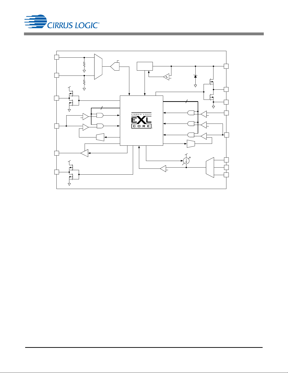
Figure 1. CS1680 Block Diagram
CS1680
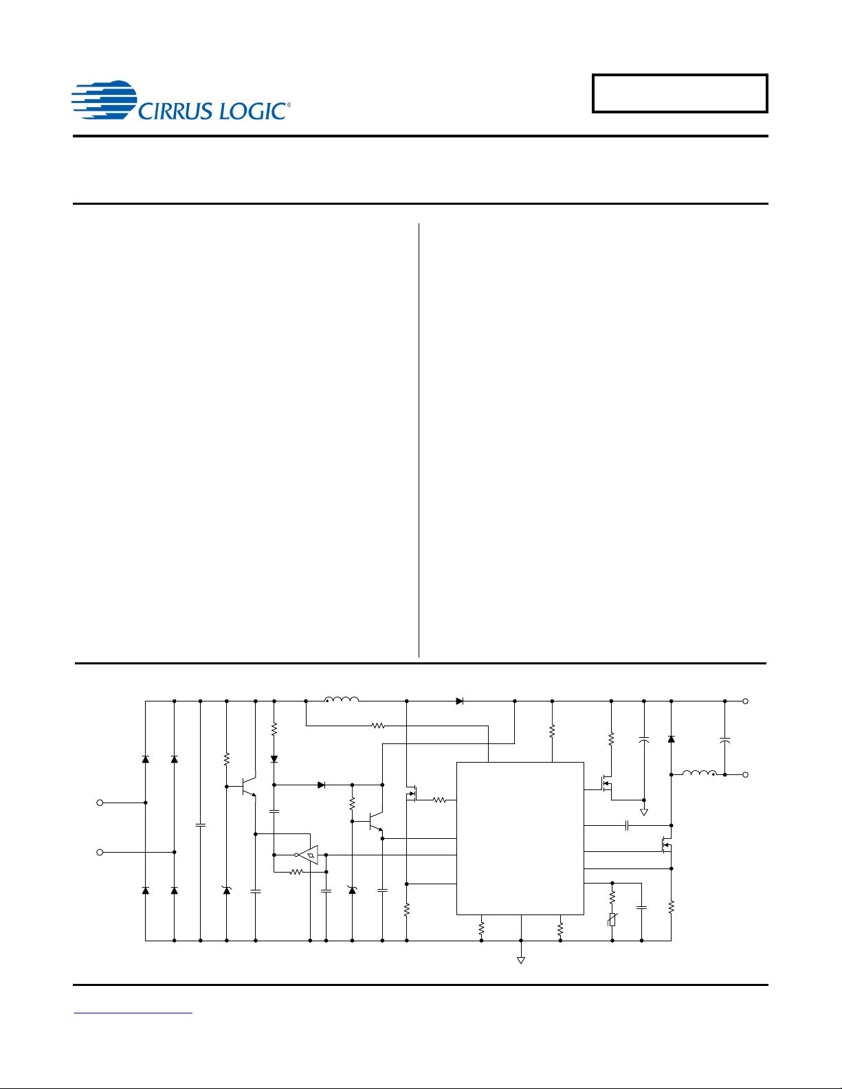
A typical schematic using the CS1680 for boost-buck
applications is shown on the previous page.
A startup circuit provides a low-impedance path to
improve electronic transformer compatibility. The GPIO
pin is used to disable the startup circuit when normal
operation is reached.
The CS1680 power supply is connected to an external
power supply network. A linear regulator at the output of
the boost converter provides steady-state operating
current to the IC. The rectified input voltage is sensed as
a current into pin VAC and is used to control the
adaptive transformer and dimmer compatibility
algorithm and extract the phase of the input voltage for
output dimming control.
During steady-state operation, the boost stage operates
in continuous conduction mode (CCM) to boost the
input voltage. This operation allows the boost stage to
2 DS1055F1
provide transformer and dimmer compatibility, reduces
bulk capacitor ripple current, and provides a regulated
input voltage to the buck stage.
The output voltage of the CCM boost is sensed by the
current into the boost output voltage sense pin
(BSTOUT). The buck stage is implemented with
peak-current mode control. Voltage across an external
user-selected resistor is sensed through pin
BUCKSENSE to control the peak current through the
buck stage inductor. Leading-edge blanking on pin
BUCKSENSE prevents false triggering.
When an external negative temperature coefficient
(NTC) thermistor is connected to the eOTP pin, the
CS1680 monitors the system temperature, allowing the
controller to reduce the output current of the system. If
the temperature reaches a designated high set point,
the IC is shutdown and stops switching.
Page 3
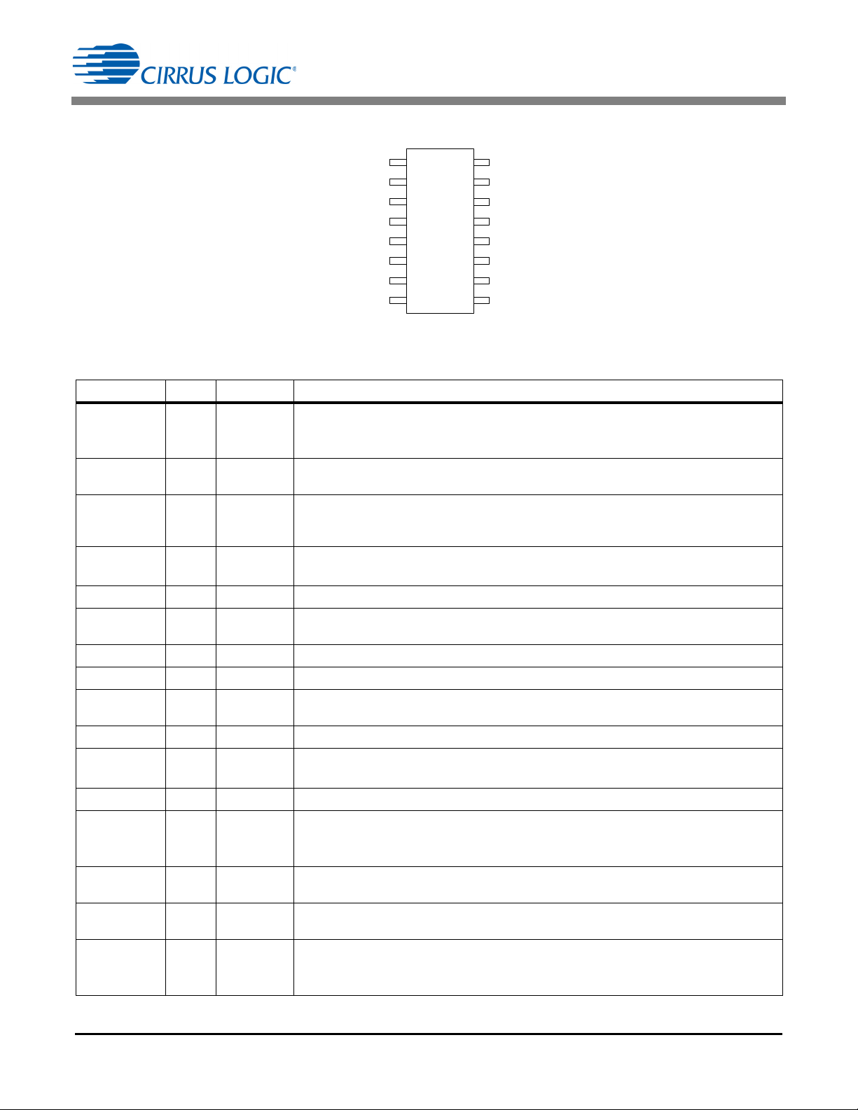
2. PIN DESCRIPTION
General Purpose Input/Output
Boost Gate Driver
Ground
Peak Current
E
xternal Overtemperature Protection
No Connect
GPIO
VDDIC Supply Voltage
BSTGD
GND
CTRL2
NC
CLAMP
BUCKGD
BUCKSENSE
VAC
BSTOUT
CTRL1
eOTP
BSTSENSEBoost Stage Current Sense
16-lead TSSOP
NC
BUCKZCD
7
6
5
4
3
2
1
10
11
12
13
14
15
16
8
9
No Connect
Voltage Clamp Current Source
Buck Gate Driver
Buck Stage Current Sense
Rectifier Voltage Sense
Boost Output Voltage Sense
Boost Stage Constant
Buck Stage Zero-current Detect
Figure 2. CS1680 Pin Assignments
CS1680
Pin Name
CTRL2
eOTP
BSTSENSE
GND
BSTGD
VDD
GPIO
NC
BUCKZCD
NC
CLAMP
BUCKGD
Pin # I/O
1IN
2IN
3IN
4PWR
5OUT
6PWR
7IN/OUT
8IN
9IN
10 IN
11 OUT
12 OUT
Description
Peak Current — Connect a resistor to this pin to set the comparator threshold to
reflect the desired boost peak current in Trailing Edge Electronic Transformer Mode (Mode 2).
External Overtemperature Protection — Connect an external NTC thermistor to
this pin, allowing the internal A/D converter to sample the change to NTC resistance.
Boost Stage Current Sense — The current flowing in the boost stage FET is
sensed across a resistor. The resulting voltage is applied to this pin and digitized for
use by the boost stage computational logic to determine the FET duty cycle.
Ground — Common reference. Current return for both the input signal portion of the
IC and the gate driver.
Boost Gate Driver — Gate drive for the boost stage power FET.
IC Supply Voltage —
operating current for the device, including the gate drive current to the power transistor
General Purpose Input/Output — Used to drive the FET gate for the startup circuit.
No Connect — Leave pin not connected.
Buck Stage Zero-current Detect — Buck stage inductor sensing input. The pin is
connected to the drain of the buck stage power FET with a capacitor.
No Connect — Leave pin not connected.
Voltage Clamp Current Source — Connect to a voltage clamp circuit on the output
of the boost stage.
Buck Gate Driver — Gate drive for the buck stage power FET.
Connect a storage capacitor to this pin to serve as a reservoir for
.
BUCKSENSE
VAC
BSTOUT
CTRL1
DS1055F1 3
13 IN
14 IN
15 IN
16 IN
Buck Stage Current Sense — The current flowing in the buck stage FET is sensed
across a resistor. The resulting voltage is applied to this pin and digitized for use by
the buck stage computational logic to determine the FET duty cycle.
Rectifier Voltage Sense — A current proportional to the rectified line voltage is fed
into this pin. The current is measured with an A/D converter.
Boost Output Voltage Sense — A current proportional to the boost output is fed
into this pin. The current is measured with an A/D converter.
Boost Stage Constant — Connect a resistor to this pin to set the constant ratio for
the boost stage current calculations in Leading Edge Electronic Transformer Mode
(Mode 3).
Page 4
CS1680
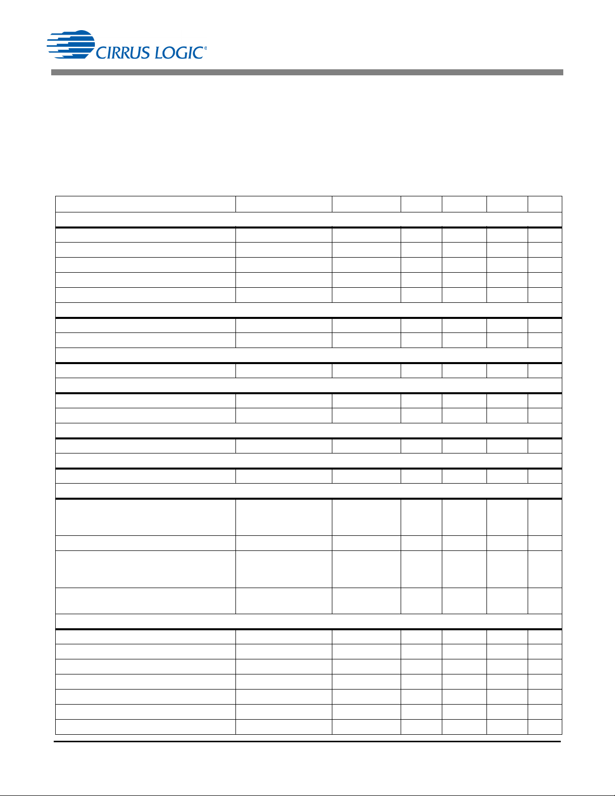
3. CHARACTERISTICS AND SPECIFICATIONS
3.1 Electrical Characteristics
Typical characteristics conditions:
=25°C, VDD= 12V, GND = 0 V
- T
A
- All voltages are measured with respect to GND.
- Unless otherwise specified, all currents are positive when
flowing into the IC.
Parameter Condition Symbol Min Typ Max Unit
VDD Supply Voltage
Operating Range
Turn-on Threshold Voltage
Turn-off Threshold Voltage (UVLO)
GPIO Low
Zener Voltage
(Note 1)
(Note 2)
After Turn-on
VDD Increasing
VDD Decreasing
V
>V
DD
I
=20mA
DD
VDD Supply Current
Startup Supply Current
Operating Supply Current
(Note 3)
VDD<V
C
= 0.25nF, fsw70 kHz
L
Reference
Reference Current I
Clamp Gate Drive
Output Source Resistance Z
Output Sink Resistance Z
Boost Output Mode1 Algorithm
Regulation Target
(Notes 1, 4) K
Boost Output Mode2 Mode Algorithm
Regulation Target
(Notes 1, 5) K
Boost Output Mode3 Algorithm
Regulation Range Low
(Notes 1, 6)
CS1680-00
CS1680-02
Regulation Range High
(Notes 1, 6) K
Accelerated Decrease On
CS1680-00
CS1680-02
Accelerated Increase On
(Notes 1, 7)
Accelerated Increase Off (Notes 1, 7)
Boost Pulse Width Modulator
Minimum On Time T1
Maximum On Time T1
Constant Off Time Mode1 T2
Minimum Off Time Mode2 & Mode3 T2
Maximum Off Time Mode2 & Mode 3 T2
Minimum Switching Frequency - 1.3 - kHz
Maximum Switching Frequency - 3.3 - MHz
Minimum/Maximum characteristics conditions:
- TJ= -40°C to +125 ° C, VDD= 11V to 17V, GND = 0 V
ST(th)
ST(th)
V
DD
V
ST(th)
V
STP(th)
K
GPIO(low)
V
I
ST
Z
11 - 17 V
-8.5-V
-7.5-V
-50.0-%
18.5 - 19.8 V
--1.0mA
-11-mA
ref
CLAMP(Source)
CLAMP(Sink)
Mode1(target)
Mode2(target)
K
Mode3(low)
-64-A
- 290 -
- 208 -
-73.3-%
-78.4-%
-
-
Mode3(high)
K
DEC(on)
-82.0-%
-
-
K
CLAMP(on)
K
CLAMP(off)
BST(min)
BST(max)
BST(fixed)
BST(min)
BST(max)
-
-
-0.1-s
- 800 - s
-0.5-s
-0.2-s
-0.9-s
60.0
65.9
52.2
60.4
87.8
85.1
-
-
-
-
-
-
%
%
%
%
%
%
4 DS1055F1
Page 5
CS1680
Parameter Condition Symbol Min Typ Max Unit
Boost Gate Driver
Output Source Resistance Z
Output Sink Resistance Z
Rise Time
Fall Time
CL=0.25nF
CL=0.25nF
BST(Source)
BST(Sink)
Boost Current Sense
Peak Control Threshold V
Leading-edge Blanking t
BSTPK(th)
BSTLEB
Delay to Output --100ns
Boost Protection
Overcurrent Protection (BOCP) V
Overvoltage Protection (BOP)
(Note 1) K
Clamp Turn-on
Clamp Turn-off
BSTOCP(th)
BOP
K
CLAMP(on)
K
CLAMP(off)
Buck Zero-Current Detect
BUCKZCD Threshold V
BUCKZCD Blanking t
ZCD Sink Current
BUCKAUX Upper Voltage
(Note 8) I
I
BUCKZCD
=1mA
BUCKZCD(th)
BUCKZCD
BUCKZCD
Buck Current Sense
Peak Control Threshold V
Leading-edge Blanking t
BUCKPK(th)
BUCKLEB
Delay to Output --100ns
Buck Pulse Width Modulator
Minimum On Time T1
BUCK(min)
Maximum On Time
CS1680-00
T1
BUCK(max)
CS1680-02
Minimum Switching Frequency - 625 - Hz
Maximum Switching Frequency - 200 - kHz
Buck Gate Driver
Output Source Resistance Z
Output Sink Resistance Z
Rise Time
Fall Time
CL=0.25nF
CL=0.25nF
BUCK(Source)
BUCK(Sink)
Buck Protection
Overcurrent Protection (OCP) V
BUCKOCP(th)
External Overtemperature Protection (eOTP), Boost Stage Constant, Peak Current
Maximum Pull-up Current Source I
Conductance Accuracy
Conductance Offset
(Note 9) --±5
(Note 9) - ±250 - nS
Current Source Voltage Threshold V
CONNECT
CONNECT(th)
- 19.9 -
- 10.5 -
-11-ns
-6-ns
-0.33- V
- 100 - ns
-1.05- V
- 93.75 -
-
-
87.8
85.1
-
-
- 200 - mV
- 250 - ns
-2 - - mA
-VDD+0.6 - V
-0.525- V
- 250 - ns
-0.55-s
-
-
12.8
25.6
-
-
s
s
- 12.7 -
-8.2-
-7.0-ns
-4.5-ns
-1.05- V
-80-A
-1.25- V
DS1055F1 5
Page 6

Parameter Condition Symbol Min Typ Max Unit
Internal Overtemperature Protection (iOTP)
Thermal Shutdown Threshold
Thermal Shutdown Hysteresis
Notes: 1. Threshold is characterized as a percentage of the full-scale boost output voltage, V
2. The CS1680 has an internal shunt regulator that limits the voltage on the VDD pin. VZ, the shunt regulation voltage, is defined in
the VDD Supply Voltage section on page 4.
3. For test purposes, load capacitance C
4. Mode1 algorithm regulates value at the trough of the rectified waveform.
5. Mode2 algorithm regulates boost output voltage at the phase cut of each rectified waveform.
6. LED output current begins changing if boost output voltage is outside the Mode 3 algorithm regulation range.
7. Accelerated increase in LED output current begins at clamp on and continues until the boost output voltage falls to clamp off.
8. External circuitry should be designed to ensure that the ZCD current drawn from the internal clamp diode when it is forward biased
does not exceed specification.
9. The conductance is specified in Siemens (S or 1/). Each LSB of the internal ADC corresponds to 250 nS or one parallel 4 M
resistor. Full scale corresponds to 256 parallel 4M resistors or 15.625 k.
10. Specifications are guaranteed by design and are characterized and correlated using statistical process methods.
(Note 10) T
(Note 10) T
is connected to gate drive pins and is equal to 0.25nF.
L
SD
SD(Hy)
3.2 Thermal Resistance
Symbol Parameter TSSOP Unit
Junction-to-Ambient Thermal Impedance 2 Layer PCB
JA
Junction-to-Case Thermal Impedance 2 Layer PCB
JC
4 Layer PCB
4 Layer PCB
CS1680
- 135 - ºC
-14-ºC
BST(full)
138
103
44
28
°C/W
°C/W
°C/W
°C/W
3.3 Absolute Maximum Ratings
Characteristics conditions:
All voltages are measured with respect to GND.
Pin Symbol Parameter Value Unit
6V
DD
1, 2, 3, 8, 9,
10, 13, 14, 15, 16
1, 2, 3, 8, 9,
10, 13, 14, 15, 16
5, 11, 12 V
5, 11, 12 I
GD
GD
-P
-T
-T
Stg
All Pins ESD
Note: 11. Transient current of up to 170mA will not cause SCR latch-up
12. Long-term operation at the maximum junction temperature will result in reduced product life. Derate internal power dissipation at
the rate of 50 mW /°C for variation over temperature.
Operation at or beyond these limits may result in permanent damage to the device.
IC Supply Voltage 18.5 V
Analog Input Maximum Voltage -0.5 to (V
Analog Input Maximum Current
Gate Drive Output Voltage -0.3 to (VDD+0.3) V
Gate Drive Output Current -1.0 / +0.5 A
Total Power Dissipation 100 mW
D
Junction Temperature Operating Range (Note 12) -40 to +125 °C
J
Storage Temperature Range -65 to +150 °C
Electrostatic Discharge Capability Human Body Model
WARNING:
Normal operation is not guaranteed at these extremes.
(Note 11) 5mA
Charged Device Model
DD
2000
500
+0.5) V
V
V
6 DS1055F1
Page 7

4. TYPICAL PERFORMANCE PLOTS
0
1
2
3
-50 0 50 100 150
UVLO Hysteresis
Temperature (ºC)
-5
0
5
10
15
20
25
30
0 2 4 6 8 101214161820
IDD (mA)
VDD (V)
7
8
9
10
-50 0 50 100 150
VDD (V)
Temperature (ºC)
Turn Off
Turn On
18
18.5
19
19.5
20
-50 0 50 100 150
V
Z
(V)
Temperature (ºC)
0
5
10
15
20
25
30
-50 0 50 100 150
Resistance (:)
Temperature (oC)
BSTGD Source
BUCKGD Source
BSTGD Sink
BUCKGD Sink
-1.75
-1.25
-0.75
-0.25
0.25
-50 0 50 100 150
Drift (%)
Temperature (C)
CS1680
Figure 3. UVLO Characteristics
Figure 5. Turn On/ Off Threshold Voltage vs. Temperature
Figure 4. Supply Current vs. Voltage
Figure 6. Zener Voltage vs. Temperature
Figure 7. Gate Drive Resistance vs. Temperature
DS1055F1 7
Figure 8. Reference Current I
Drift vs. Temperature
ref
Page 8

5. GENERAL DESCRIPTION
CS1680
5.1 Overview
The CS1680 is a cascade boost-buck dimmable LED
driver for the 12V halogen lamp-replacement market.
The CS1680 uses a Cirrus Logic proprietary intelligent
digital control that provides exceptional single-lamp and
multi-lamp transformer compatibility for non-dimmer
systems and dimmer systems paired with electronic and
magnetic low-voltage transformers.
The CS1680 integrates a continuous conduction mode
(CCM) boost converter that provides transformer
compatibility and dimmer compatibility. An adaptive
digital algorithm controls the boost stage and dimmer
compatibility operation mode to enable flicker-free
operation down to 5% output current with leading-edge
and trailing-edge dimmers.
5.2 IC Startup and Power Supply
The startup circuit is constructed of a linear regulator
and charge pump, and is used to supply a power-on
voltage to the CS1680. The device provides a GPIO pin
that is used to disable the startup circuit once the boost
output voltage reaches 50% of full scale.
The linear regulator circuit uses transistor Q1 to provide
a supply voltage to a Schmitt-trigger inverter which
enables the charge pump circuit. The GPIO pin is
tri-stated while the controller is held in reset due to low
supply voltage. The charge pump increases the voltage
until the device starts converting. Once the supply
voltage V
exceeds threshold voltage V
DD
ST(th)
, the
controller polls the boost output voltage for 50% of full
scale before driving the GPIO pin low to disable the
startup circuit.
5.3 Boost Stage
The boost stage in the CS1680 is a low-side
asynchronous boost converter. Once the IC reaches its
UVLO start threshold voltage V
operating, the CS1680 executes a detection algorithm
to set the operating state of the IC (see Table 1 on
page 8). The boost stage utilizes a continuous current
mode (CCM) control algorithm.
5.3.1 Dimmer Compatibility
The CS1680 dimmer switch detection algorithm
determines if the solid-state lighting (SSL) system is
controlled: first, using a regular switch or a leading-edge
dimmer paired with a magnetic transformer, or a
12VAC/VDC source (Mode1); second, by a regular
switch or a trailing-edge dimmer paired with an electronic
and begins
ST(th)
transformer (Mode2); third, by a leading-edge dimmer
paired with an electronic transformer (Mode3).
Boost
Mode
Mode1
Mode2
Mode3
Source Line Switch Digital Control Loop
12 VAC/VDC Non-dimming
Magnetic
Transformer
Electronic
Transformer
Electronic
Transformer
Leading-edge
Dimmer
Non-dimming
Trailing-edge
Dimmer
Non-dimming
Leading-edge
Dimmer
Table 1. Operating State
Executes a boost peakcurrent algorithm with
PFC based control.
Executes a constant
boost peak-current
algorithm during the turnon time of the electronic
transformer.
Executes a constant
power control algorithm
where the boost inductor
current is controlled by
the instantaneous
rectified voltage signal.
Dimmer switch detection is implemented using a
process of elimination. The method of elimination
progresses through the detection algorithm to find the
best matching state of operation. In an attempt to find a
dimmer compatible mode, the detection algorithm starts
in Mode1, then tries Mode2, if Mode1 and Mode2 are
excluded the algorithm defaults to Mode3.
Mode1
In Mode1, the detectable inputs are a leading-edge
dimmer paired with a magnetic transformer, no dimmer
switch paired with a magnetic transformer, or a
12VDC/VAC source. Upon detection of a magnetic
transformer, the CS1680 operates in a PFC conduction
mode where the device provides a power factor that is
in excess of 0.9. The boost peak current I
BSTPK
is
modulated across the input voltage to follow a constant
resistance. The target resistance is modulated to
provide boost output regulation. The RMS input voltage
is used to determine the output LED current as a
fraction of full scale. If a DC input voltage is detected,
the controller will set the LED output at 100% of the
available RMS energy.
The boost output voltage V
is measured at the
BST
trough of the rectified voltage every half-line cycle and
compared against the regulation point, which is set by
resistor R
difference, the setting of LED output current I
(see Figure 11 on page 10). The voltage
BST
OUT
, and
the clamp activity are used in the control loop to scale
the boost inductor current allowing the boost output
8 DS1055F1
Page 9

CS1680
Regulation Range High
Regulation Range Low
Accelerated Decrease On
Accelerated Increase On
Accelerated Increase Off
V
BST
u
K
Mode 3(high)
V
BST
u
K
CLAMP(off)
V
BST
u
K
CLAMP(on)
V
BST
u
K
Mode 3(low)
V
BST
u
K
DEC(on)
t
v(t)
Voltage Threshold
Figure 9. Mode3 Output Regulation Algorithm
voltage to reach the regulation target set by
constant K
Mode1(target)
. If boost output voltage V
BST
below the target regulation point or the boost output
voltage is falling, the boost inductor current is increased.
If the boost output voltage is above the target regulation
point, the boost output voltage is rising, or the clamp has
been activated recently the boost current is decreased.
The LED output current is set using a third-order
polynomial of the rectified RMS voltage, computed over
a half-line cycle and filtered to avoid lamp flicker.
Mode2
In Mode 2, the CS1680 will detect if the input is a trailing
edge dimmer paired with an electronic transformer or no
dimmer switch paired with an electronic transformer. The
detection algorithm determines its operation based on
the falling edge of the input voltage waveform. To provide
proper dimmer operation, the CS1680 executes the
peak current inversely proportional to the boost output
voltage. The algorithm attempts to maintain a constant
is
power while limiting the boost peak current to prevent
saturating the boost inductor.
The Mode1 and Mode2 algorithms use properties of the
input waveform on a cycle-by-cycle basis to determine
the output current, and then adjusts the boost control
parameters to balance the input power with the
requested output power. Unlike the Mode1 and Mode2
algorithms, the Mode3 algorithm leaves the boost
parameters fixed and adjusts the output current to
balance input power and output power. As long as boost
output voltage V
remains between the voltage
BST
thresholds set by lower regulation range
constant K
constant K
Mode3(low)
Mode3(high)
and higher regulation range
, the LED output current I
remain constant (see Figure 9).
OUT
will
boost algorithm on the falling edge of the input line
voltage, which will maintain a charge in the dimmer
capacitor. To ensure maximum compatibility with dimmer
components, the device boosts during this falling edge
event using a peak current that must meet a minimum
value.
The boost output voltage V
is measured at the
BST
trailing edge of the rectified voltage every half-line cycle
and compared against the regulation point, which is set
by resistor R
(see Figure 11 on page 10). The
BST
voltage difference, the setting of LED output
current I
, and the clamp activity are used in the
OUT
control loop to modulate the boost turn-on time every
half-line cycle which allows the boost output voltage to
reach the regulation target set by constant
K
Mode2(target)
. If boost output voltage V
is below the
BST
target regulation point or the boost output voltage is
falling, the total turn-on time over a half-line cycle is
increased. If the boost output voltage is above the target
regulation point, the boost output voltage is rising, or the
clamp has been activated recently, the total turn-on time
over a half-line cycle is decreased. The Mode2
algorithm estimates the turn-on time of the transformer
by measuring the conduction angle of the rectified
voltage every half-line cycle. The LED output current is
set based on the output power requirements for a
particular conduction angle by the regulation loop.
Mode3
In Mode 3, the CS1680 will detect if the input is a leading
edge dimmer paired with an electronic transformer. The
CS1680 regulates boost output voltage V
maintaining the dimmer phase angle. The device
executes a CCM boost algorithm that keeps the boost
BST
while
If the boost output voltage V
regulation range high voltage threshold set by
constant K
Mode3(high)
(due to the phase angle of the
dimmer increasing which allows for the first stage to
produce additional power), LED output current I
gradually increased until the boost output voltage V
falls below the regulation range high threshold. The rate
of increase continues to add larger steps as long as
boost output voltage V
stays above the regulation
BST
high threshold. If the boost output voltage continues to
rise and reaches the clamp-on threshold set by
constant K
CLAMP(on)
, the clamp circuit will activate to
dissipate the excess power from the boost output. While
the clamp is on, the LED output current I
at an accelerated rate.
If the boost output voltage V
regulation range low voltage threshold set by
constant K
Mode3(low)
, LED output current I
gradually decreased. The rate of decrease continues to
subtract larger steps as long as the boost output voltage
stays below the regulation range low threshold. If the
rises above the
BST
increases
OUT
falls below the
BST
OUT
OUT
is
BST
is
DS1055F1 9
Page 10

CS1680
T1
BSTi
T2
BSTi
B
STGD
I
L
I
PKBST
IL = 0
Figure 10. Continuous Conduction Mode Operation
I
BSTPK max
V
BSTPK th
R
BST Sense
-------------------------------- -=
[Eq.1]
I
BSTPK OCP
V
BSTOCP th
R
BST Sense
---------------------------------=
[Eq.2]
D
BST
V
rec t
V
BST
R
rect
CS1680
I
BSTOUT
BSTOU T
VAC
ADC
I
ref
20 k
20 k
MUX
15
14
I
VAC
R
BST
L
BST
Figure 11. VAC and BSTOUT Input Pin Model
V
BST fullIrefRBST
20k+=
[Eq.3]
boost output voltage continues to fall and reaches the
lowest threshold set by constant K
DEC(on)
, the LED
output current is decreased at an accelerated rate.
If the LED output current I
boost output voltage V
BST
is at a maximum and
OUT
is still above the regulation
high threshold, the controller begins scaling down the
boost inductor current instead of increasing the LED
output current. If this happens, when the boost output
voltage falls below the regulation low threshold, the
boost input current is gradually increased back to
nominal before the LED output current begins to reduce
off from the maximum.
5.3.2 Boost Stage Control
The boost stage uses continuous conduction mode
operation for high compatibility with electronic
transformers. For current regulation, the controller
varies the peak current I
and transformer compatibility. When the dimmer is
paired with an electronic transformer, period T2
modulated to maintain a constant ripple current on the
boost inductor. When the dimmer is paired with a
magnetic transformer, the demagnetization period has
a constant T2
BST(fixed)
time.
as necessary for dimmer
BSTPK
BST
is
after one second. The boost overcurrent protection
current I
BSTPK(OCP)
is calculated using Equation 2:
Output BSTOUT Sense and Input VAC Sense
A current proportional to boost output voltage V
BST
is
supplied to the IC on pin BSTOUT and is used as a
control signal (see Figure 11). The ADC is used to
measure the magnitude of current I
resistor R
. The magnitude of current I
BST
BSTOUT
compared to an internal full scale reference current I
BSTOUT
through
is then
ref
of 64A.
Maximum Peak Current
The maximum boost inductor peak current I
is set using the current sense resistor R
pin BSTSENSE, which is sampled by a comparator
referenced to an internal DAC. Boost peak current
I
BSTPK(max)
is calculated using Equation 1:
Boost overcurrent protection (BOCP) is provided using
a higher threshold to detect the event of inductor
saturation. If the voltage on the BSTSENSE pin
exceeds a threshold voltage V
controller enters a BOCP fault. The IC output is
disabled, the gate drive output pins BSTGD and
BUCKGD turn off, and the controller attempts to restart
10 DS1055F1
BSTOCP(th)
BSTPK(max)
BST(Sense)
on
of 1.05V, the
Resistor R
determines boost output voltage V
sets the system full-scale voltage and
BST
regulation, boost
BST
overvoltage protection, and clamp behavior. Full-scale
voltage V
BST(full)
The CS1680-00 is designed for a resistor R
is calculated using Equation 3:
BST
equal to
604k, creating a full-scale voltage of 40V. The
CS1680-02 is designed for a resistor R
equal to
BST
560k, creating a full-scale voltage of 37V.
A current proportional to the AC/DC input voltage is
supplied to the IC on pin VAC and is used by the boost
control algorithm. Dimmer detection and dim level
calculations are dependent on specific levels of the line
voltage. Resistor R
is required to be set equal to
rec
604k
For optimal performance, resistors R
rect
and R
BST
should use 1% or better resistors for best voltage
accuracy.
Boost Overvoltage Protection
The CS1680 supports boost overvoltage protection
(BOP) to protect bulk capacitor C
(see Figure 13 on
BST
Page 11

CS1680
V
BOP thVBST fullKBOP
=
[Eq.4]
CLAMP
R
CLAMP
V
BST
CS1680
11
C
BST
VDD
EXL
Core
Q
CLAMP
Figure 12. CLAMP Pin Model
V
CLAMP onVBST fullKCLAMP on
=
[Eq.5]
V
CLAMP offVBST fullKCLAMP off
=
[Eq.6]
GND
BUCKGD
BUC KSENSE
CS1680
R
BUCK( Sense)
Q
BUCK
LED +
LED -
V
BST
C
BST
D
BUCK
C
OUT
13
12
4
C4
BUCKZCD
9
L
BUCK
Figure 13. Buck Model
page 11). If the boost output voltage exceeds the
overvoltage protection threshold, a BOP fault signal is
generated. Boost overvoltage threshold V
BOP(th)
is
calculated using Equation 4:
For a nominal system design where resistor R
equals 604k and full-scale voltage V
40V, this sets threshold voltage V
BOP(th)
BST(full)
to 37.4V.
BST
equals
The control logic continuously averages this BOP fault
signal, and if at any point in time the average exceeds a
set event threshold, the boost stage is disabled.
5.3.3 Voltage Clamp Circuit
During transient events and interactions with electronic
transformers, it is possible for the boost stage to
generate more power than is consumed by the second
stage. A clamping circuit is added to the system to
dissipate the excess power. The CS1680 provides
active clamp circuitry on pin CLAMP, as shown in
Figure 12.
clamp circuit. If the cumulative turn-on time exceeds
200ms during the internally generated 2-second
window time, a COP event is actuated, disabling the
boost and buck stages. The clamp circuitry is turned off
during the fault event.
5.4 Buck Stage
The second stage is a current-regulated buck converter,
delivering the highest possible efficiency at a constant
current while minimizing line frequency ripple. A buck
stage is illustrated in Figure 13. Primary-side control is
used to simplify system design and reduce system cost
and complexity.
When operating with a dimmer, the dimming signal is
extracted in the time domain and is proportional to the
conduction angle of the dimmer. A control variable is
The clamp circuit is enabled when boost output
voltage V
voltage V
on until boost output voltage V
clamp turn-off threshold voltage V
voltage V
exceeds the clamp turn-on threshold
BST
CLAMP(on)
CLAMP(on)
. The clamp circuit will remain turned
is lowered below the
BST
CLAMP(off)
. Threshold
is calculated using Equation 5:
passed to the second stage to achieve 5% to 100%
output currents.
The buck stage control parameters assures the LED
current remains constant despite a ±10% line voltage
variation (line regulation), and the LED current remains
constant over a ± 20% variation in buck inductor
inductance.
Threshold voltage V
Equation 6:
CLAMP(off)
is calculated using
5.4.1 Buck Inductor Model
The BUCKSENSE input is used to sense the buck
inductor current. When the current reaches a certain
threshold, the gate drive turns off (output on pin
BUCKGD). The sensed current and internal calculation
are used to determine the switching period TT
Clamp Overpower Protection
The CS1680 clamp overpower protection (COP) control
logic continuously monitors the turn-on time of the
DS1055F1 11
The zero-current detect input on pin BUCKZCD is used
to determine the buck inductor zero-crossing
BUCK
.
Page 12

CS1680
I
BUCKPK max
V
BUCKPK th
R
BUCK Sense
------------------------------------ -=
[Eq.7]
I
BUCKPK OCP
V
BUCKOCP th
R
BUCK Sense
-------------------------------------=
[Eq.8]
CS1680
+
-
I
CONNECT
V
CONNECT
(th)
Comp_Out
eOTP
Control
eOTP
R
S
C
NTC
NTC
V
DD
2
(Optional)
Figure 14. eOTP Functional Diagram
period T2
time TT
BUCK
. The controller then uses the
BUCK
to determine gate turn-on time.
5.4.2 Current Sense Resistor Model
The digital algorithm ensures monotonic dimming from
5% to 100 % of the dimming range with a linear
relationship between the dimming signal and the LED
current. The buck stage is regulated by peak current
control with a 1% external sense resistor R
BUCK(Sense)
connected to the BUCKSENSE pin. Buck peak current
I
BUCKPK(max)
is calculated using Equation 7:
Overcurrent protection (OCP) is implemented by
monitoring the voltage across buck sense
resistor R
BUCK(Sense)
threshold voltage V
. If this voltage exceeds a
BUCKOCP(th)
of 1.05 V, a fault
condition occurs. The IC output is disabled, the gate
drive output pins BSTGD and BUCKGD turn off, and the
controller attempts to restart after one second. The buck
overcurrent protection current I
BUCKPK(OCP)
is
calculated using Equation 8:
5.4.3 Zero-current Detection
Zero-current switching is achieved by detecting the
buck inductor current zero-crossing using a capacitive
coupling network. The digital control algorithm rejects
line-frequency ripple created on the second-stage input
by the front-end boost stage, resulting in the highest
possible LED efficiency and long LED life.
5.5 Overtemperature Protection
The CS1680 incorporates both internal overtemperature
protection (iOTP) and the ability to connect an external
overtemperature sense circuit for IC protection. Typically, a negative temperature coefficient (NTC) thermistor is
used.
5.5.1 Internal Overtemperature Protection
Internal overtemperature protection (iOTP) is activated,
and switching is disabled when the die temperature of
the devices exceeds 135 °C. There is a hysteresis of
about 14°C before resuming normal operation.
5.5.2 External Overtemperature Protection
The external overtemperature protection (eOTP) pin is
used to implement overtemperature protection. A negative
temperature coefficient (NTC) thermistor resistive network
is connected to pin eOTP, usually in the form of a series
combination of a resistor R
and a thermistor R
S
NTC
(see
Figure 14). The CS1680 cyclically samples the resistance
connected to pin eOTP.
The total resistance on the eOTP pin gives an indication of
the temperature and is used in a digital feedback loop to
adjust current I
series resistor R
V
CONNECT(th)
of 1.25V. Current I
CONNECT
to maintain a constant reference voltage
S
into the NTC thermistor and
CONNECT
is generated
from a controlled current source with a full-scale current of
80A. When the loop is in equilibrium, the voltage on pin
eOTP fluctuates around voltage V
resistance ADC is used to generate I
CONNECT
CONNECT(th)
. A
. The ADC
output is filtered to suppress noise and compared against
a reference that corresponds to 125°C. A second low-pass
filter with a time constant of two seconds filters the ADC
output and is used to scale down the internal dim level of
the system (and hence LED current I
LED
) if the
temperature exceeds 95 °C. The large time constant for
this filter ensures that the dim scaling does not happen
spontaneously and is not noticeable (suppress spurious
glitches). The eOTP tracking circuit is designed to function
accurately with external capacitance up to 470pF.
The tracking range of this resistance ADC is approximately
15.5k to 4 M. The series resistor R
is used to adjust
S
the resistance of the NTC thermistor to fall within the ADC
tracking range, allowing the entire dynamic range of the
ADC to be well used. The CS1680 recognizes a resistance
(R
S+RNTC
) equal to 20.3k which corresponds to a
temperature of 95°C, as the beginning of an
overtemperature dimming event and starts reducing the
power dissipation. The output current is scaled until the
series resistance (R
S+RNTC
) value reaches 16.6k
(125°C). Beyond this temperature, the IC enters a fault
state and shuts down. This fault state is a latched
protection state, and the fault state is not cleared until the
power to the IC is recycled.
12 DS1055F1
Page 13

When exiting reset, the chip enters startup and the ADC
Temperature (°C)
Current (I
LED
, Nom. )
125
95
50%
100%
0
25
Figure 15. LED Current vs. eOTP Temperature
quickly (<15 ms) tracks the external temperature to check
if it is below 120°C reference code before the controller is
powered up. If this check fails, the chip will wait until this
condition becomes true before initializing the rest of the
system; that is, until the resistance (R
S+RNTC
) rises above
17.02k.
For example, a 14 k (±1% tolerance) series resistor is
required to allow measurements of up to 130°C to be
within the eOTP tracking range when a 100k NTC with a
Beta of 4275. If the temperature exceeds 95°C,
thermistor R
resistor R
is approximately 6.3k and series
NTC
is 14k, so the eOTP pin has a total resistance
S
of 20.3k. The eOTP pin initiates protective dimming
action by reducing the power dissipation. At 125°C, the
thermistor R
has 2.6k plus a series resistor RS equal
NTC
to 14k present a resistance of 16.6k at the eOTP pin
reaching the point where a thermal shutdown fault
CS1680
intervenes. The CS1680 fault state is not cleared until the
power to the IC is recycled (see Figure 15).
If the external overtemperature protection feature is not
required, connect the eOTP pin to GND using a
50k-to-500k resistor to disable the eOTP feature.
DS1055F1 13
Page 14

6. PACKAGE DRAWING
16L TSSOP (170 MIL BODY) PACKAGE DRAWING
CS1680
Dimension MIN NOM MAX MIN NOM MAX
A -- -- 1.1 -- -- 0.043
A1 0.05 -- 0.15 0.002 -- 0.006
A2 0.85 -- 0.95 0.033 -- 0.037
b 0.19 -- 0.27 0.007 -- 0.011
b1 0.19 -- 0.25 0.007 -- 0.010
c 0.13 -- 0.18 0.005 -- 0.007
c1 0.09 -- 0.14 0.004 -- 0.006
D 4.9 5 5.1 0.193 0.197 0.201
E1 4.3 4.4 4.5 0.169 0.173 0.177
E 6.3 6.4 6.5 0.248 0.252 0.256
e 0.65BSC 0.026BSC
L 0.5 0.6 0.7 .020 0.024 0.028
L1 1REF 0.039REF
Θ10°--8°0°--8°
Θ2 12°TYP 12° TYP
Θ3 12°TYP 12° TYP
R1 0.09 -- -- 0.004 -- --
mm inch
14 DS1055F1
Page 15

Dimension MIN NOM MAX MIN NOM MAX
R2 0.09 -- -- 0.004 -- --
S 0.2 -- -- 0.008 - --
aaa 0.2 0.008
bbb 0.1 0.004
ccc 0.1 0.004
ddd 0.05 0.002
Notes:
1. Controlling dimensions are in millimeters.
2. Dimensions and tolerances per ASME Y14.5 M.
3. This drawing conforms to JEDEC outline MS-012, variation AC for standard 16L TSSOP narrow body.
4. Recommended reflow profile is per JEDEC/IPC J-STD-020.
7. ORDERING INFORMATION
CS1680
mm inch
Ordering Number AC Line Voltage Temperature Package Description
CS1680-FZZ Bulk
12VAC/VDC -40 °C to +125 °C
CS1680-FZZR Tape & Reel 3.09.1
CS168002-FZZ Bulk
12VAC/VDC -40 °C to +125 °C
CS168002-FZZR Tape & Reel 3.07.2
16-lead TSSOP,
Lead (Pb) Free
16-lead TSSOP,
Lead (Pb) Free
Configuration
Version
3.09.1
3.07.2
8. ENVIRONMENTAL, MANUFACTURING, & HANDLING INFORMATION
Part Number Peak Reflow Temp MSL Rating
CS1680-FZZ 260 °C 3 7 Days
CS168002-FZZ 260 °C 3 7 Days
a. MSL (Moisture Sensitivity Level) as specified by IPC/JEDEC J-STD-020.
b. Stored at 30°C, 60% relative humidity.
a
Max Floor Life
b
DS1055F1 15
Page 16

REVISION HISTORY
Contacting Cirrus Logic Support
For all product questions and inquiries contact a Cirrus Logic Sales Representative.
To find one nearest you go to http://www.cirrus.com
IMPORTANT NOTICE
Cirrus Logic, Inc. and its subsidiaries (“Cirrus”) believe that the information contained in this document is accurate and reliable. However, the information is subject
to change without notice and is provided “AS IS” without warranty of any kind (express or implied). Customers are advised to obtain the latest version of relevant
information to verify, before placing orders, that information being relied on is current and complete. All products are sold subject to the terms and conditions of sale
supplied at the time of order acknowledgment, including those pertaining to warranty, indemnification, and limitation of liability. No responsibility is assumed by Cirrus
for the use of this information, including use of this information as the basis for manufacture or sale of any items, or for infringement of patents or other rights of third
parties. This document is the property of Cirrus and by furnishing this information, Cirrus grants no license, express or implied under any patents, mask work rights,
copyrights, trademarks, trade secrets or other intellectual property rights. Cirrus owns the copyrights associated with the information contained herein and gives consent for copies to be made of the information only for use within your organization with respect to Cirrus integrated circuits or other products of Cirrus. This consent
does not extend to other copying such as copying for general distribution, advertising or promotional purposes, or for creating any work for resale.
CERTAIN APPLICATIONS USING SEMICONDUCTOR PRODUCTS MAY INVOLVE POTENTIAL RISKS OF DEATH, PERSONAL INJURY, OR SEVERE PROPERTY OR ENVIRONMENTAL DAMAGE (“CRITICAL APPLICATIONS”). CIRRUS PRODUCTS ARE NOT DESIGNED, AUTHORIZED OR WARRANTED FOR USE
IN PRODUCTS SURGICALLY IMPLANTED INTO THE BODY, AUTOMOTIVE SAFETY OR SECURITY DEVICES, LIFE SUPPORT PRODUCTS OR OTHER CRITICAL APPLICATIONS. INCLUSION OF CIRRUS PRODUCTS IN SUCH APPLICATIONS IS UNDERSTOOD TO BE FULLY AT THE CUSTOMER'S RISK AND CIRRUS DISCLAIMS AND MAKES NO WARRANTY, EXPRESS, STATUTORY OR IMPLIED, INCLUDING THE IMPLIED WARRANTIES OF MERCHANTABILITY AND
FITNESS FOR PARTICULAR PURPOSE, WITH REGARD TO ANY CIRRUS PRODUCT THAT IS USED IN SUCH A MANNER. IF THE CUSTOMER OR CUSTOMER'S CUSTOMER USES OR PERMITS THE USE OF CIRRUS PRODUCTS IN CRITICAL APPLICATIONS, CUSTOMER AGREES, BY SUCH USE, TO FULLY
INDEMNIFY CIRRUS, ITS OFFICERS, DIRECTORS, EMPLOYEES, DISTRIBUTORS AND OTHER AGENTS FROM ANY AND ALL LIABILITY, INCLUDING ATTORNEYS' FEES AND COSTS, THAT MAY RESULT FROM OR ARISE IN CONNECTION WITH THESE USES.
Use of the formulas, equations, calculations, graphs, and/or other design guide information is at your sole discretion and does not guarantee any specific results or
performance. The formulas, equations, graphs, and/or other design guide information are provided as a reference guide only and are intended to assist but not to be
solely relied upon for design work, design calculations, or other purposes. Cirrus Logic makes no representations or warranties concerning the formulas, equations,
graphs, and/or other design guide information.
Cirrus Logic, Cirrus, the Cirrus Logic logo designs, EXL Core, and the EXL Core logo design are trademarks of Cirrus Logic, Inc. All other brand and product names
in this document may be trademarks or service marks of their respective owners.
Revision Date Changes
PP1 JAN 2014 Content updates for revision B silicon
PP2 FEB 2014 Content update for configuration version 3.07.2
F1 OCT 2014 Final release
CS1680
16 DS1055F1
 Loading...