

Page 1
CS1630
D7
R13
NTC
Z2
BR1 BR1
AC
Mains
C7
L1
D2
BR1 BR 1
D5
C8
R11
L2
D6
C2
R4
R8
R14
R6
R7
Q4
Q2
Z1 C4
CS1630 /31
IAC
SOURCE
FBAUX
BSTOUT
GNDSGND
13
16
5
4
CLAMP
GD
FBSENSE
eOTP
15
10
12
11
1
2
BSTAUX
C3
R2
D1
Q3
R10
3
R
S
C
NTC
T1
R1
C1
R5
C6
D4
D3
C5
Q1
R9
R3
V
BST
V
rect
14
VDD
R12
D9
C9
C11
C12
D11
D8
R15 D10
Q5
R16
C10
Z3
IGND
LED2 +
LED 1+
LED 1-
LED2 -
D
GND
_QVCC
CS1631
2-Channel TRIAC Dimmable LED Driver IC
Features
• Best-in-class Dimmer Compatibility
- Leading-edge (TRIAC) Dimmers
- Trailing-edge Dimmers
- Digital Dimmers (with Integrated Power Supply)
• Correlated Color Temperature (CCT) Control System
• Up to 85% Efficiency
• Flicker-free Dimming
• Programmable Dimming Profile
- Constant CCT Dimming
- Black Body Line Dimming
• 0% Minimum Dimming Level
• Temperature Compensated LED Current
• End-of-line Programming Using Power Line Calibration
- Lower LED Binning Requirement
• Programmable Series or Parallel Two-Channel Output
- Interleaved Output Eliminates Additional Transformer
• Programmable Quasi-resonant Second Stage with
Constant-current Output
- Flyback, Buck, and Tapped Buck
• Register Lockout
• Fast Startup
• Tight LED Current Regulation: Better than ±5%
• Primary-side Regulation (PSR)
• >0.9 Power Factor
• IEC-61000-3-2 Compliant
• Soft Start
• Protections:
- Output Open/Short
- Current-sense Resistor Open/Short
- External Overtemperature Using NTC
Overview
The CS1630 and CS1631 are high-performance offline AC /DC
LED drivers for dimmable and high color rendering index (CRI)
LED replacement lamps and luminaires. They feature Cirrus
Logic’s proprietary digital dimmer compatibility control technology
and digital correlated color temperature (CCT) control system that
enables two-channel LED color mixing. The CS1630 is designed
for 120VAC line voltage applications, and the CS1631 is
optimized for 230VAC line voltage applications.
The CS1630/31 integrates a critical conduction mode boost
converter, providing power factor correction and superior dimmer
compatibility with a primary-side regulated quasi-resonant second
stage, which is configurable for isolated and non-isolated
topologies. The digital CCT control system provides the ability to
program dimming profiles, such as constant CCT dimming and
black body line dimming. The CS1630/31 optimizes LED color
mixing by temperature compensating LED current with an
external NTC. The IC controller is also equipped with power line
calibration for remote system calibration and end-of-line
programming. The CS1630/31 provides a register lockout feature
for security against potential access to proprietary registers.
Applications
• Dimmable Retrofit LED Lamps and LED Luminaries
• High CRI Lighting
• Offline LED Drivers
• Commercial Lighting
Ordering Information
See page 55.
Cirrus Logic, Inc.
http://www.cirrus.com
Copyright Cirrus Logic, Inc. 2013
(All Rights Reserved)
APR’13
DS954F3
Page 2

CS1630/31
TABLE OF CONTENTS
1.INTRODUCTION . . . . . . . . . . . . . . . . . . . . . . . . . . . . . . . . . . . . . . . . . . . . . . . . . . . . . . . . . . . . . . . . . . . . . 4
2.PIN DESCRIPTION . . . . . . . . . . . . . . . . . . . . . . . . . . . . . . . . . . . . . . . . . . . . . . . . . . . . . . . . . . . . . . . . . . . 5
3.CHARACTERISTICS AND SPECIFICATIONS. . . . . . . . . . . . . . . . . . . . . . . . . . . . . . . . . . . . . . . . . . . . . . 6
3.1 Electrical Characteristics . . . . . . . . . . . . . . . . . . . . . . . . . . . . . . . . . . . . . . . . . . . . . . . . . . . . . . . . . . . . . . . . . . . . . . . .6
2
3.2 I
C™ Port Switching Characteristics . . . . . . . . . . . . . . . . . . . . . . . . . . . . . . . . . . . . . . . . . . . . . . . . . . . . . . . . . . . . . . .8
3.3 Power Line Calibration Characteristics . . . . . . . . . . . . . . . . . . . . . . . . . . . . . . . . . . . . . . . . . . . . . . . . . . . . . . . . . . . . . .9
3.4 Thermal Resistance . . . . . . . . . . . . . . . . . . . . . . . . . . . . . . . . . . . . . . . . . . . . . . . . . . . . . . . . . . . . . . . . . . . . . . . . . . .10
3.5 Absolute Maximum Ratings . . . . . . . . . . . . . . . . . . . . . . . . . . . . . . . . . . . . . . . . . . . . . . . . . . . . . . . . . . . . . . . . . . . . .10
4.TYPICAL PERFORMANCE PLOTS . . . . . . . . . . . . . . . . . . . . . . . . . . . . . . . . . . . . . . . . . . . . . . . . . . . . . 11
5.GENERAL DESCRIPTION . . . . . . . . . . . . . . . . . . . . . . . . . . . . . . . . . . . . . . . . . . . . . . . . . . . . . . . . . . . . 12
5.1 Overview . . . . . . . . . . . . . . . . . . . . . . . . . . . . . . . . . . . . . . . . . . . . . . . . . . . . . . . . . . . . . . . . . . . . . . . . . . . . . . . . . . . .12
5.2 Startup Circuit . . . . . . . . . . . . . . . . . . . . . . . . . . . . . . . . . . . . . . . . . . . . . . . . . . . . . . . . . . . . . . . . . . . . . . . . . . . . . . . .12
5.3 Dimmer Switch Detection . . . . . . . . . . . . . . . . . . . . . . . . . . . . . . . . . . . . . . . . . . . . . . . . . . . . . . . . . . . . . . . . . . . . . . .12
5.3.1 Dimmer Learn Mode . . . . . . . . . . . . . . . . . . . . . . . . . . . . . . . . . . . . . . . . . . . . . . . . . . . . . . . . . . . . . . . . . . . . 12
5.3.2 Dimmer Validate Mode. . . . . . . . . . . . . . . . . . . . . . . . . . . . . . . . . . . . . . . . . . . . . . . . . . . . . . . . . . . . . . . . . . . 12
5.3.3 No-dimmer Mode . . . . . . . . . . . . . . . . . . . . . . . . . . . . . . . . . . . . . . . . . . . . . . . . . . . . . . . . . . . . . . . . . . . . . . . 12
5.3.4 Leading-edge Mode . . . . . . . . . . . . . . . . . . . . . . . . . . . . . . . . . . . . . . . . . . . . . . . . . . . . . . . . . . . . . . . . . . . . . 12
5.3.5 Trailing-edge Mode . . . . . . . . . . . . . . . . . . . . . . . . . . . . . . . . . . . . . . . . . . . . . . . . . . . . . . . . . . . . . . . . . . . . . 13
5.4 Correlated Color Temperature Control . . . . . . . . . . . . . . . . . . . . . . . . . . . . . . . . . . . . . . . . . . . . . . . . . . . . . . . . . . . . .13
5.5 Dimming Signal Extraction and the Dim Mapping Algorithm . . . . . . . . . . . . . . . . . . . . . . . . . . . . . . . . . . . . . . . . . . . .14
5.6 Boost Stage . . . . . . . . . . . . . . . . . . . . . . . . . . . . . . . . . . . . . . . . . . . . . . . . . . . . . . . . . . . . . . . . . . . . . . . . . . . . . . . . .14
5.6.1 Maximum Peak Current . . . . . . . . . . . . . . . . . . . . . . . . . . . . . . . . . . . . . . . . . . . . . . . . . . . . . . . . . . . . . . . . . . 14
5.6.2 Output BSTOUT Sense & Input IAC Sense. . . . . . . . . . . . . . . . . . . . . . . . . . . . . . . . . . . . . . . . . . . . . . . . . . . 15
5.6.3 Boost Auxiliary Winding . . . . . . . . . . . . . . . . . . . . . . . . . . . . . . . . . . . . . . . . . . . . . . . . . . . . . . . . . . . . . . . . . . 15
5.6.4 Boost Overvoltage Protection . . . . . . . . . . . . . . . . . . . . . . . . . . . . . . . . . . . . . . . . . . . . . . . . . . . . . . . . . . . . . 15
5.7 Voltage Clamp Circuit . . . . . . . . . . . . . . . . . . . . . . . . . . . . . . . . . . . . . . . . . . . . . . . . . . . . . . . . . . . . . . . . . . . . . . . . . .15
5.7.1 Clamp Overpower Protection . . . . . . . . . . . . . . . . . . . . . . . . . . . . . . . . . . . . . . . . . . . . . . . . . . . . . . . . . . . . . . 16
5.8 Quasi-resonant Second Stage . . . . . . . . . . . . . . . . . . . . . . . . . . . . . . . . . . . . . . . . . . . . . . . . . . . . . . . . . . . . . . . . . . .16
5.8.1 Series & Parallel Two-Channel Output . . . . . . . . . . . . . . . . . . . . . . . . . . . . . . . . . . . . . . . . . . . . . . . . . . . . . . 17
5.8.2 Primary-side Current Control for Two-Channel Output . . . . . . . . . . . . . . . . . . . . . . . . . . . . . . . . . . . . . . . . . . 18
5.8.3 Auxiliary Winding Configuration . . . . . . . . . . . . . . . . . . . . . . . . . . . . . . . . . . . . . . . . . . . . . . . . . . . . . . . . . . . . 18
5.8.4 Control Parameters . . . . . . . . . . . . . . . . . . . . . . . . . . . . . . . . . . . . . . . . . . . . . . . . . . . . . . . . . . . . . . . . . . . . . 18
5.8.5 Frequency Dithering. . . . . . . . . . . . . . . . . . . . . . . . . . . . . . . . . . . . . . . . . . . . . . . . . . . . . . . . . . . . . . . . . . . . . 18
5.8.6 Output Open Circuit Protection . . . . . . . . . . . . . . . . . . . . . . . . . . . . . . . . . . . . . . . . . . . . . . . . . . . . . . . . . . . . 19
5.8.7 Overcurrent Protection . . . . . . . . . . . . . . . . . . . . . . . . . . . . . . . . . . . . . . . . . . . . . . . . . . . . . . . . . . . . . . . . . . . 19
5.8.8 Open Loop Protection . . . . . . . . . . . . . . . . . . . . . . . . . . . . . . . . . . . . . . . . . . . . . . . . . . . . . . . . . . . . . . . . . . . 19
5.9 Overtemperature Protection . . . . . . . . . . . . . . . . . . . . . . . . . . . . . . . . . . . . . . . . . . . . . . . . . . . . . . . . . . . . . . . . . . . . .19
5.9.1 Internal Overtemperature Protection . . . . . . . . . . . . . . . . . . . . . . . . . . . . . . . . . . . . . . . . . . . . . . . . . . . . . . . . 19
5.9.2 External Overtemperature Protection. . . . . . . . . . . . . . . . . . . . . . . . . . . . . . . . . . . . . . . . . . . . . . . . . . . . . . . . 19
5.10 Power Line Calibration . . . . . . . . . . . . . . . . . . . . . . . . . . . . . . . . . . . . . . . . . . . . . . . . . . . . . . . . . . . . . . . . . . . . . . . . .21
5.10.1 Power Line Calibration Specification . . . . . . . . . . . . . . . . . . . . . . . . . . . . . . . . . . . . . . . . . . . . . . . . . . . . . . . . 21
5.10.2 PLC Program Mode Characters. . . . . . . . . . . . . . . . . . . . . . . . . . . . . . . . . . . . . . . . . . . . . . . . . . . . . . . . . . . . 22
5.10.3 Calibration Mode Operation Code . . . . . . . . . . . . . . . . . . . . . . . . . . . . . . . . . . . . . . . . . . . . . . . . . . . . . . . . . . 22
5.10.4 Register Lockout . . . . . . . . . . . . . . . . . . . . . . . . . . . . . . . . . . . . . . . . . . . . . . . . . . . . . . . . . . . . . . . . . . . . . . . 23
2
5.11 I
C™ Communication Interface . . . . . . . . . . . . . . . . . . . . . . . . . . . . . . . . . . . . . . . . . . . . . . . . . . . . . . . . . . . . . . . . . .23
5.11.1 I
5.11.2 Control Port Enable . . . . . . . . . . . . . . . . . . . . . . . . . . . . . . . . . . . . . . . . . . . . . . . . . . . . . . . . . . . . . . . . . . . . . 24
5.11.3 Read Operation . . . . . . . . . . . . . . . . . . . . . . . . . . . . . . . . . . . . . . . . . . . . . . . . . . . . . . . . . . . . . . . . . . . . . . . . 24
5.11.4 Write Operation . . . . . . . . . . . . . . . . . . . . . . . . . . . . . . . . . . . . . . . . . . . . . . . . . . . . . . . . . . . . . . . . . . . . . . . . 25
5.11.5 Customer I
5.12 OTP Memory . . . . . . . . . . . . . . . . . . . . . . . . . . . . . . . . . . . . . . . . . . . . . . . . . . . . . . . . . . . . . . . . . . . . . . . . . . . . . . . .26
5.12.1 Programming the OTP Memory . . . . . . . . . . . . . . . . . . . . . . . . . . . . . . . . . . . . . . . . . . . . . . . . . . . . . . . . . . . . 26
2
C Control Port Protocol . . . . . . . . . . . . . . . . . . . . . . . . . . . . . . . . . . . . . . . . . . . . . . . . . . . . . . . . . . . . . . . . . 23
2
C Lockout . . . . . . . . . . . . . . . . . . . . . . . . . . . . . . . . . . . . . . . . . . . . . . . . . . . . . . . . . . . . . . . . . . . 25
2 DS954F3
Page 3

CS1630/31
6.ONE-TIME PROGRAMMABLE (OTP) REGISTERS . . . . . . . . . . . . . . . . . . . . . . . . . . . . . . . . . . . . . . . . 27
6.1 Registers Map . . . . . . . . . . . . . . . . . . . . . . . . . . . . . . . . . . . . . . . . . . . . . . . . . . . . . . . . . . . . . . . . . . . . . . . . . . . . . . .27
6.2 Configuration 0 (Config0) – Address 0 . . . . . . . . . . . . . . . . . . . . . . . . . . . . . . . . . . . . . . . . . . . . . . . . . . . . . . . . . . . . .29
6.3 Lockout Key (LOCK0, LOCK1, LOCK2, LOCK3) – Address 1 - 4 . . . . . . . . . . . . . . . . . . . . . . . . . . . . . . . . . . . . . . . .29
6.4 Color Polynomial Coefficient (P30, P20, P10, P03, P02, P01, P21, P12, P11, P00) – Address 5 - 24 . . . . . . . . . . . .29
6.5 Color Polynomial Coefficient (Q3, Q2, Q1, Q0) – Address 25 - 32 . . . . . . . . . . . . . . . . . . . . . . . . . . . . . . . . . . . . . . .30
6.6 Gate Drive Duration (GD_DUR) – Address 33 . . . . . . . . . . . . . . . . . . . . . . . . . . . . . . . . . . . . . . . . . . . . . . . . . . . . . . .30
6.7 Configuration 2 (Config2) – Address 34 . . . . . . . . . . . . . . . . . . . . . . . . . . . . . . . . . . . . . . . . . . . . . . . . . . . . . . . . . . . .31
6.8 Configuration 3 (Config3) – Address 35 . . . . . . . . . . . . . . . . . . . . . . . . . . . . . . . . . . . . . . . . . . . . . . . . . . . . . . . . . . . .32
6.9 Configuration 4 (Config4) – Address 36 . . . . . . . . . . . . . . . . . . . . . . . . . . . . . . . . . . . . . . . . . . . . . . . . . . . . . . . . . . . .33
6.10 Second Stage Dim (S2DIM) – Address 37 . . . . . . . . . . . . . . . . . . . . . . . . . . . . . . . . . . . . . . . . . . . . . . . . . . . . . . . . . .33
6.11 Maximum TT (TTMAX) – Address 38 . . . . . . . . . . . . . . . . . . . . . . . . . . . . . . . . . . . . . . . . . . . . . . . . . . . . . . . . . . . . . .33
6.12 Configuration 7 (Config7) – Address 39 . . . . . . . . . . . . . . . . . . . . . . . . . . . . . . . . . . . . . . . . . . . . . . . . . . . . . . . . . . . .34
6.13 Configuration 8 (Config8) – Address 40 . . . . . . . . . . . . . . . . . . . . . . . . . . . . . . . . . . . . . . . . . . . . . . . . . . . . . . . . . . . .34
6.14 Channel 1 Output Current (CH1CUR) – Address 41 . . . . . . . . . . . . . . . . . . . . . . . . . . . . . . . . . . . . . . . . . . . . . . . . . .35
6.15 Configuration 10 (Config10) – Address 42 . . . . . . . . . . . . . . . . . . . . . . . . . . . . . . . . . . . . . . . . . . . . . . . . . . . . . . . . . .35
6.16 Channel 2 Output Current (CH2CUR) – Address 43 . . . . . . . . . . . . . . . . . . . . . . . . . . . . . . . . . . . . . . . . . . . . . . . . . .35
6.17 Configuration 12 (Config12) – Address 44 . . . . . . . . . . . . . . . . . . . . . . . . . . . . . . . . . . . . . . . . . . . . . . . . . . . . . . . . . .36
6.18 PU Coefficient (PID) – Address 45 . . . . . . . . . . . . . . . . . . . . . . . . . . . . . . . . . . . . . . . . . . . . . . . . . . . . . . . . . . . . . . . .36
6.19 Maximum Switching Frequency (TTFREQ) – Address 46 . . . . . . . . . . . . . . . . . . . . . . . . . . . . . . . . . . . . . . . . . . . . . .36
6.20 Configuration 15 (Config15) – Address 47 . . . . . . . . . . . . . . . . . . . . . . . . . . . . . . . . . . . . . . . . . . . . . . . . . . . . . . . . . .37
6.21 Configuration 16 (Config16) – Address 48 . . . . . . . . . . . . . . . . . . . . . . . . . . . . . . . . . . . . . . . . . . . . . . . . . . . . . . . . . .37
6.22 Configuration 17 (Config17) – Address 49 . . . . . . . . . . . . . . . . . . . . . . . . . . . . . . . . . . . . . . . . . . . . . . . . . . . . . . . . . .38
6.23 Configuration 18 (Config18) – Address 50 . . . . . . . . . . . . . . . . . . . . . . . . . . . . . . . . . . . . . . . . . . . . . . . . . . . . . . . . . .38
6.24 Peak Current (PEAK_CUR) – Address 51 . . . . . . . . . . . . . . . . . . . . . . . . . . . . . . . . . . . . . . . . . . . . . . . . . . . . . . . . . .39
6.25 Configuration 38 (Config38) – Address 70 . . . . . . . . . . . . . . . . . . . . . . . . . . . . . . . . . . . . . . . . . . . . . . . . . . . . . . . . . .39
6.26 Configuration 44 (Config44) – Address 76 . . . . . . . . . . . . . . . . . . . . . . . . . . . . . . . . . . . . . . . . . . . . . . . . . . . . . . . . . .39
6.27 Configuration 45 (Config45) – Address 77 . . . . . . . . . . . . . . . . . . . . . . . . . . . . . . . . . . . . . . . . . . . . . . . . . . . . . . . . . .40
6.28 Configuration 46 (Config46) – Address 78 . . . . . . . . . . . . . . . . . . . . . . . . . . . . . . . . . . . . . . . . . . . . . . . . . . . . . . . . . .40
6.29 Configuration 47 (Config47) – Address 79 . . . . . . . . . . . . . . . . . . . . . . . . . . . . . . . . . . . . . . . . . . . . . . . . . . . . . . . . . .41
6.30 Configuration 48 (Config48) – Address 80 . . . . . . . . . . . . . . . . . . . . . . . . . . . . . . . . . . . . . . . . . . . . . . . . . . . . . . . . . .42
6.31 Configuration 49 (Config49) – Address 81 . . . . . . . . . . . . . . . . . . . . . . . . . . . . . . . . . . . . . . . . . . . . . . . . . . . . . . . . . .42
6.32 Configuration 50 (Config50) – Address 82 . . . . . . . . . . . . . . . . . . . . . . . . . . . . . . . . . . . . . . . . . . . . . . . . . . . . . . . . . .43
6.33 Configuration 51 (Config51) – Address 83 . . . . . . . . . . . . . . . . . . . . . . . . . . . . . . . . . . . . . . . . . . . . . . . . . . . . . . . . . .43
6.34 Configuration 52 (Config52) – Address 84 . . . . . . . . . . . . . . . . . . . . . . . . . . . . . . . . . . . . . . . . . . . . . . . . . . . . . . . . . .44
6.35 Configuration 53 (Config53) – Address 85 . . . . . . . . . . . . . . . . . . . . . . . . . . . . . . . . . . . . . . . . . . . . . . . . . . . . . . . . . .45
6.36 Configuration 54 (Config54) – Address 86 . . . . . . . . . . . . . . . . . . . . . . . . . . . . . . . . . . . . . . . . . . . . . . . . . . . . . . . . . .46
6.37 Configuration 55 (Config55) – Address 87 . . . . . . . . . . . . . . . . . . . . . . . . . . . . . . . . . . . . . . . . . . . . . . . . . . . . . . . . . .47
6.38 PLC Dim (PLC_DIM) – Address 89 . . . . . . . . . . . . . . . . . . . . . . . . . . . . . . . . . . . . . . . . . . . . . . . . . . . . . . . . . . . . . . .47
6.39 Configuration 58 (Config58) – Address 90 . . . . . . . . . . . . . . . . . . . . . . . . . . . . . . . . . . . . . . . . . . . . . . . . . . . . . . . . . .48
6.40 Configuration 59 (Config59) – Address 91 . . . . . . . . . . . . . . . . . . . . . . . . . . . . . . . . . . . . . . . . . . . . . . . . . . . . . . . . . .48
6.41 Configuration 60 (Config60) – Address 92 . . . . . . . . . . . . . . . . . . . . . . . . . . . . . . . . . . . . . . . . . . . . . . . . . . . . . . . . . .49
6.42 Configuration 61 (Config61) – Address 93 . . . . . . . . . . . . . . . . . . . . . . . . . . . . . . . . . . . . . . . . . . . . . . . . . . . . . . . . . .49
6.43 Configuration 62 (Config62) – Address 94 . . . . . . . . . . . . . . . . . . . . . . . . . . . . . . . . . . . . . . . . . . . . . . . . . . . . . . . . . .50
6.44 CRC Tag (CRC_TAG) – Address 102 . . . . . . . . . . . . . . . . . . . . . . . . . . . . . . . . . . . . . . . . . . . . . . . . . . . . . . . . . . . . .50
6.45 Channel 1 Color Calibration 3A (CH1_CAL3A) – Address 119 . . . . . . . . . . . . . . . . . . . . . . . . . . . . . . . . . . . . . . . . . .51
6.46 Channel 2 Color Calibration 3A (CH2_CAL3A) – Address 120 . . . . . . . . . . . . . . . . . . . . . . . . . . . . . . . . . . . . . . . . . .51
6.47 CRC Memory Tag 3A (CRC_MTAG3A) – Address 121 . . . . . . . . . . . . . . . . . . . . . . . . . . . . . . . . . . . . . . . . . . . . . . . .51
6.48 Channel 1 Color Calibration 3B (CH1_CAL3B) – Address 122 . . . . . . . . . . . . . . . . . . . . . . . . . . . . . . . . . . . . . . . . . .52
6.49 Channel 2 Color Calibration 3B (CH2_CAL3B) – Address 123 . . . . . . . . . . . . . . . . . . . . . . . . . . . . . . . . . . . . . . . . . .52
6.50 CRC Memory Tag 3B(CRC_MTAG3B) – Address 124 . . . . . . . . . . . . . . . . . . . . . . . . . . . . . . . . . . . . . . . . . . . . . . . .52
6.51 Channel 1 Color Calibration 3C (CH1_CAL3C) – Address 125 . . . . . . . . . . . . . . . . . . . . . . . . . . . . . . . . . . . . . . . . . .53
6.52 Channel 2 Color Calibration 3C (CH2_CAL3C) – Address 126 . . . . . . . . . . . . . . . . . . . . . . . . . . . . . . . . . . . . . . . . . .53
6.53 CRC Memory Tag 3C (CRC_MTAG3C) – Address 127 . . . . . . . . . . . . . . . . . . . . . . . . . . . . . . . . . . . . . . . . . . . . . . . .53
7.PACKAGE DRAWING . . . . . . . . . . . . . . . . . . . . . . . . . . . . . . . . . . . . . . . . . . . . . . . . . . . . . . . . . . . . . . . 54
8.ORDERING INFORMATION . . . . . . . . . . . . . . . . . . . . . . . . . . . . . . . . . . . . . . . . . . . . . . . . . . . . . . . . . . . 55
9.ENVIRONMENTAL, MANUFACTURING, & HANDLING INFORMATION . . . . . . . . . . . . . . . . . . . . . . . 55
10.REVISION HISTORY. . . . . . . . . . . . . . . . . . . . . . . . . . . . . . . . . . . . . . . . . . . . . . . . . . . . . . . . . . . . . . . . 56
DS954F3 3
Page 4
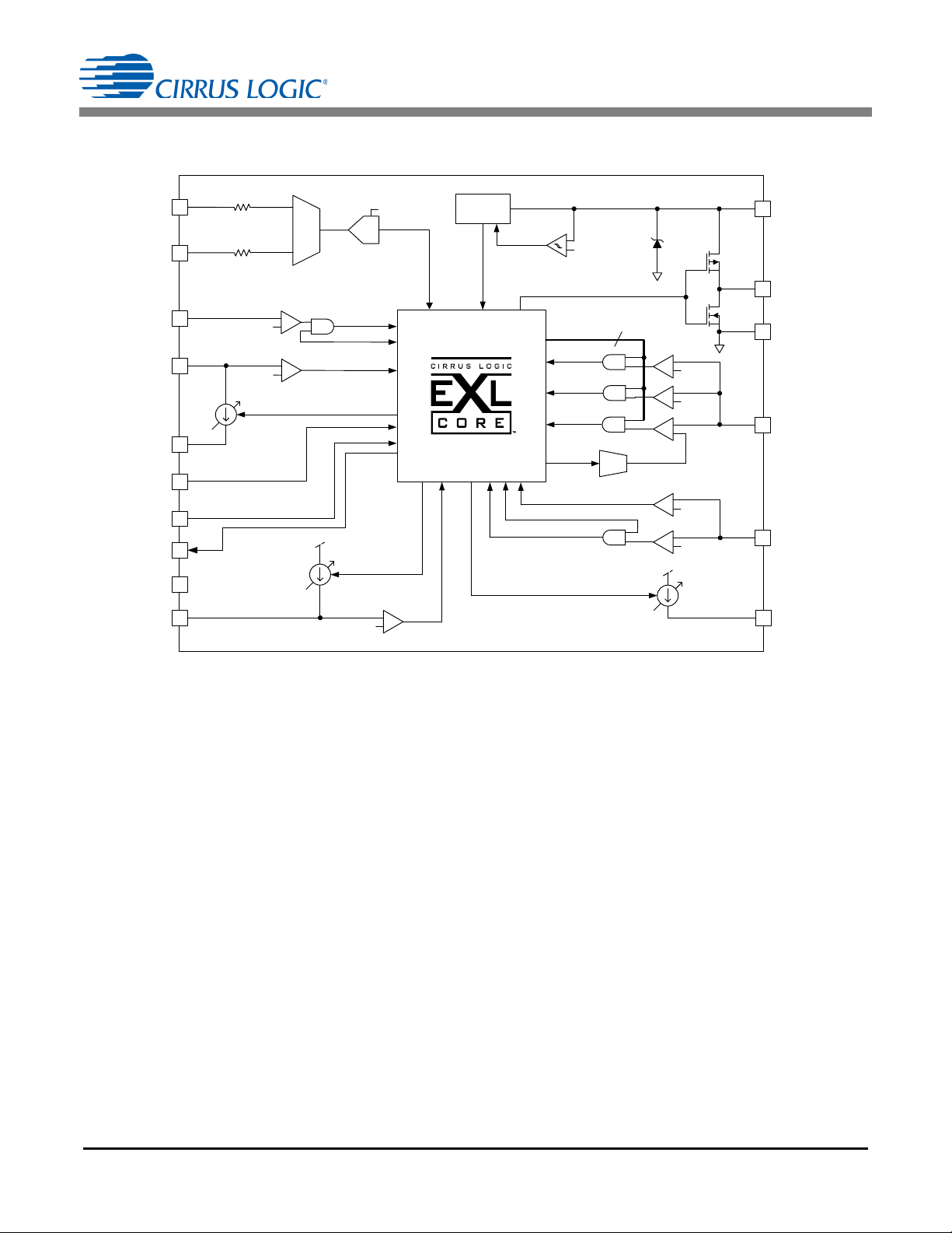
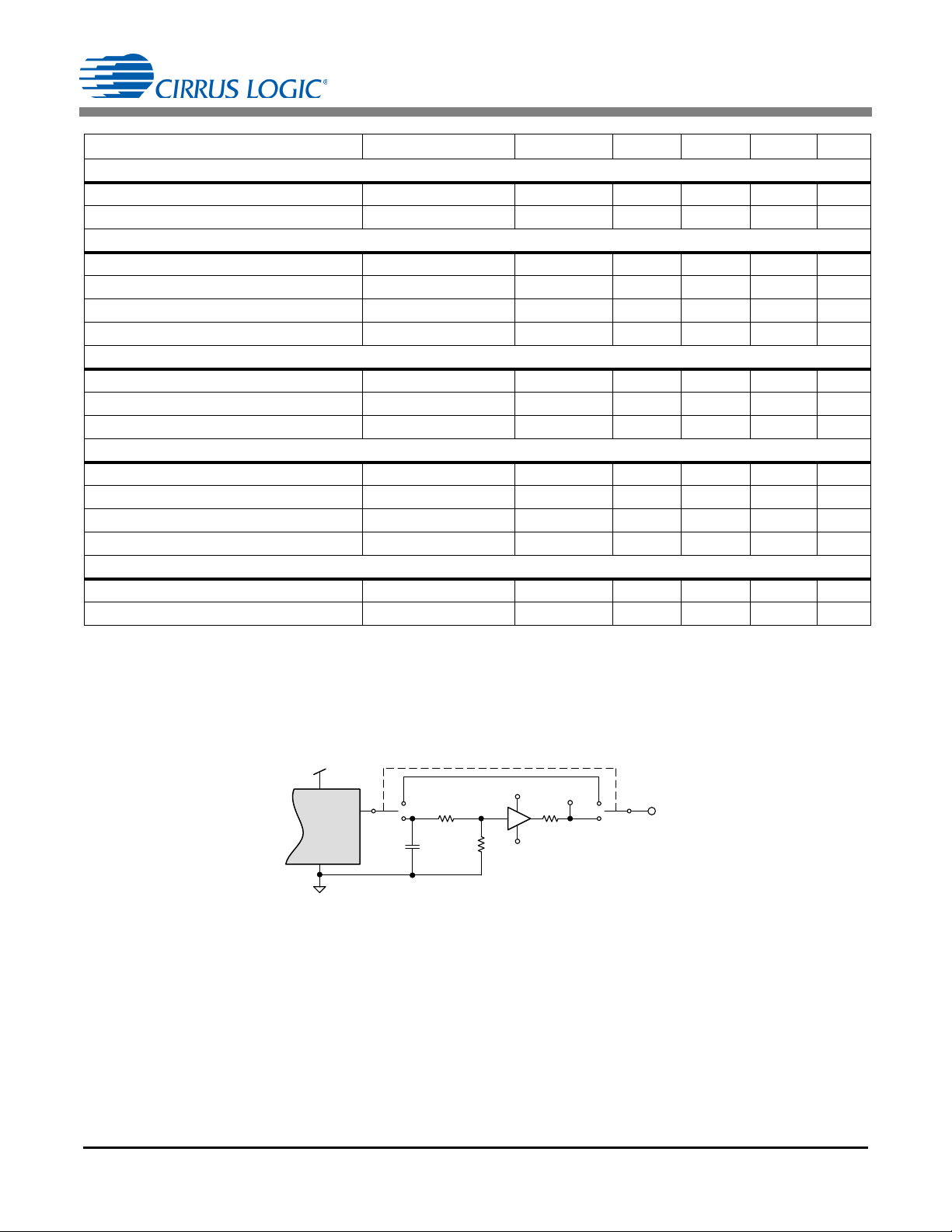
1. INTRODUCTION
V
Z
POR
+
-
Volt age
Regul ator
14
VDD
11
FBSENSE
+
-
15
FBAUX
+
-
13
GD
2
IAC
DAC
+
-
Peak
Contr ol
Fl yback Z CD
+
-
Output O pen
12
GND
OLP
+
-
16
BSTOUT
OCP
+
-
1
BSTAUX
Boost Z CD
3
CLAMP
V
ST(th )
V
STP(th )
V
OCP(th)
V
FBZC D(th)
V
OVP (th )
V
OLP(th)
V
FBZC D(th)
V
Pk_Max(th)
10
4
SGND
5
SOURCE
+
-
+
-
VDD
I
CONNECT
V
CONNECT(th)
V
SOURCE(th)
7
SCL
6
SDA
8
NC
9
SYNC
eOTP
15 k
ADC
MUX
15k
VDD
I
ref
t
FBZC D
I
CLAMP
t
BSTZCD
I
SOURCE
Blank 3
CS1630/31
Figure 1. CS1630/31 Block Diagram
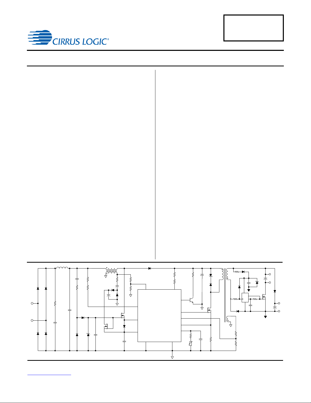
A typical schematic using the CS1630/31 IC is shown on the
front page.
Startup current is provided from a patent-pending, external
high-voltage source-follower network. In addition to providing
startup current, this unique topology is integral in providing
compatibility with digital dimmers by ensuring V
always available to the IC. During steady-state operation, an
auxiliary winding on the boost inductor back-biases the
DD
power is
source-follower circuit and provides steady-state operating
current to the IC to improve system efficiency.
The rectified input voltage is sensed as a current into pin IAC
and is used to control the adaptive dimmer compatibility
algorithm and extract the phase of the input voltage for output
dimming control. During steady-state operation, the external
high-voltage, source-follower circuit is source-switched in
critical conduction mode (CRM) to boost the input voltage.
This allows the boost stage to maintain good power factor,
provide dimmer compatibility, reduce bulk capacitor ripple
current, and provide a regulated input voltage to the second
stage.
The current into the boost output voltage sense pin BSTOUT
senses the output voltage of the CRM boost front-end.
4 DS954F3
The quasi-resonant second stage is implemented with peakcurrent mode primary-side control, which eliminates the need
for additional components to provide feedback from the
secondary and reduces system cost and complexity.
Voltage across an external user-selected resistor is sensed
through pin FBSENSE to control the peak current through the
second stage inductor. Leading-edge and trailing-edge
blanking on pin FBSENSE prevents false triggering.
Pin FBAUX is used to sense the second stage inductor
demagnetization to ensure quasi-resonant switching of the
output stage.
An internal current source is adjusted by a feedback loop to
regulate a constant reference voltage on pin eOTP for external
negative temperature coefficient (NTC) thermistor
measurements. An external NTC is connected to pin eOTP to
provide thermal protection of the system and LED temperature
compensation. The output current of the system is steadily
reduced when the system temperature exceeds a
programmable temperature set point. If the temperature
reaches a designated high set point, the IC is shutdown and
stops switching.
Page 5
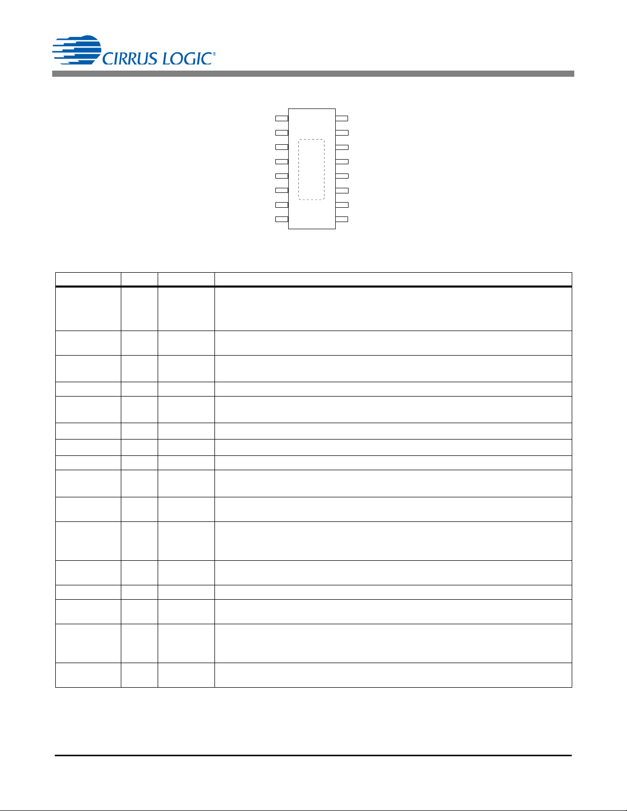
2. PIN DESCRIPTION
I2C Clock
Source Switch
Source Ground
Boost Zero-current Detect
Rectifier Voltage Sense
No Connection
SCL
SDAI
2
C Data
SOURCE
SGND
BSTAUX
eOTP
FBSENSE
GND
GD Gate Driver
VDD
IC Supply Voltage
FBAUX
Second Stage Zero-current Detect
BSTOUT
Boost Output Voltage Sense
IAC
CLAMP
V
oltage Clamp Current Source
16-lead SOIC
NC
SYNC
7
6
5
4
3
2
1
10
11
12
13
14
15
16
8
9
External Overtemperature Protection
Second Stage Current Sense
Ground
Second Stage Synchronization
Figure 2. CS1630/31
CS1630/31
Pin Name
BSTAUX
IAC
CLAMP
SGND
SOURCE
SDA
SCL
NC
SYNC
eOTP
FBSENSE
GND
GD
VDD
FBAUX
BSTOUT
DS954F3 5
Pin # I/O
1IN
2IN
3OUT
4PWR
5IN
6 I/O
7IN
8-
9OUT
10 IN
11 IN
12 PWR
13 OUT
14 PWR
15 IN
16 IN
Description
Boost Zero-current Detect — Boost Inductor demagnetization sensing input for
zero-current detection (ZCD) information. The pin is connected to the PFC boost
inductor auxiliary winding through an external resistor divider.
Rectifier Voltage Sense — A current proportional to the rectified line voltage is fed
into this pin. The current is measured with an A/D converter.
Voltage Clamp Current Source — Connect to a voltage clamp circuit on the output
of the boost stage.
Source Ground — Common reference current return for the SOURCE pin.
Source Switch — Connected to the source of the boost stage external high-voltage
FET.
I2C™ Data — I2C data.
I2C™ Clock — I2C clock.
No Connection — Leave pin unconnected.
Second Stage Synchronization — A digital synchronization signal that indicates
which channel the controller is signaling for each gate switching period.
External Overtemperature Protection — Connect an external NTC thermistor to
this pin, allowing the internal A/D converter to sample the change to NTC resistance.
Second Stage Current Sense — The current flowing in the second stage FET is
sensed across a resistor. The resulting voltage is applied to this pin and digitized for
use by the second stage computational logic to determine the FET's duty cycle.
Ground — Common reference. Current return for both the input signal portion of the
IC and the gate driver.
Gate Driver — Gate drive for the second stage power FET.
IC Supply Voltage
— Connect a storage capacitor to this pin to serve as a reservoir for
operating current for the device, including the gate drive current to the power transistor.
Second Stage Zero-current Detect — Second stage inductor sensing input. The
pin is connected to the second stage inductor’s auxiliary winding through an external
resistor divider.
Boost Output Voltage Sense — A current proportional to the boost output is fed
into this pin. The current is measured with an A/D converter.
Page 6
CS1630/31
3. CHARACTERISTICS AND SPECIFICATIONS
3.1 Electrical Characteristics
Typical characteristics conditions:
=25ºC, VDD= 12V, GND = 0V
•T
A
• All voltages are measured with respect to GND.
• Unless otherwise specified, all currents are positive
when flowing into the IC.
Parameter Condition Symbol Min Typ Max Unit
VDD Supply Voltage
Operating Range After Turn-on V
Turn-on Threshold Voltage V
Turn-off Threshold Voltage (UVLO) V
Zener Voltage (Note 1) I
Increasing V
DD
Decreasing V
DD
=20mA V
DD
VDD Supply Current
Startup Supply Current V
Operating Supply Current (Note 5)
DD<VST(th)
CL= 0.25nF, Fsw60 kHz
Reference
Reference Current
V
CS1630
CS1631
= 200 V
BST
V
= 400 V
BST
Boost
Maximum Switching Frequency f
Clamp Current I
Dimmer Attach Peak Current
CS1630
CS1631
108 V
207 V
line
line
Boost Zero-current Detect
BSTZCD Threshold V
ZCD Sink Current (Note 2) I
BSTAUX Upper Voltage I
BSTZCD
Boost Protection
Clamp Turn-on
CS1630
CS1631
108 V
207 V
line
line
Second Stage Zero-current Detect
FBZCD Threshold V
ZCD Sink Current (Note 2) I
FBAUX Upper Voltage I
=1mA - VDD+0.6 - V
FBZCD
Second Stage Current Sense
Peak Control Threshold V
Delay to Output --100ns
Minimum/Maximum characteristics conditions:
= -40°C to +125°C, VDD= 11V to 17V, GND = 0 V
•T
J
DD
ST(th)
STP(th)
Z
I
ST
11 - 17 V
-8.5-V
-7.5-V
18.5 - 19.8 V
--200A
-5.8-mA
132
253
I
ref
BST(Max)
CLAMP
BSTZCD(th)
BSTZCD
-
-
--200kHz
--3.8-mA
-
-
-200-mV
-2 - - mA
133
133
590
508
-
-
-
-
A
A
mA
mA
=1mA - VDD+0.6 - V
132
253
FBZCD(th)
FBZCD
Pk_Max(th)
-
-
-200-mV
-2 - - mA
-1.4-V
146.7
141.7
-
-
A
A
6 DS954F3
Page 7
CS1630/31
GD OU T
GD
GND
VDD
Buffer
S
1
R
1
R
2
R
3
TP
+15V
-15V
S
2
V
DD
C
L
0.25 nF
Parameter Condition Symbol Min Typ Max Unit
Second Stage Pulse Width Modulator
Minimum Switching Frequency t
Maximum Switching Frequency t
FB(Min)
FB(Max)
Second Stage Gate Driver
Output Source Resistance
Output Sink Resistance
Rise Time (Note 5)
Fall Time (Note 5)
VDD=12V
VDD=12V
CL=0.25nF
CL=0.25nF
Second Stage Protection
Overcurrent Protection (OCP) V
Overvoltage Protection (OVP) V
Open Loop Protection (OLP) V
OCP(th)
OVP(th)
OLP(th)
External Overtemperature Protection (eOTP)
Pull-up Current Source – Maximum I
CONNECT
Conductance Accuracy (Note 3) - - ±5
Conductance Offset (Note 3) - ± 250 - nS
Current Source Voltage Threshold V
CONNECT(th)
Internal Overtemperature Protection (iOTP)
Thermal Shutdown Threshold (Note 4) T
Thermal Shutdown Hysteresis (Note 4) T
Notes: 1. The CS1630/31 has an internal shunt regulator that limits the voltage on the VDD pin. VZ, the shunt regulation voltage, is defined
in the VDD Supply Voltage section on page 6.
2. External circuitry should be designed to ensure that the ZCD current drawn from the internal clamp diode when it is forward biased
does not exceed specification.
3. Conductance is the inverse of resistance (1/) and is expressed in siemens (S). A decrease in conductance is equivalent to an
increase in resistance.
4. Specifications are guaranteed by design and are characterized and correlated using statistical process methods.
5. For test purposes, load capacitance (C
) is 0.25nF and is connected as shown in the following diagram.
L
SD
SD(Hy)
-625-Hz
-200-kHz
-24-
-11-
--30ns
--20ns
-1.69-V
-1.25-V
-200-mV
-80-A
-1.25-V
-135-ºC
-14-ºC
DS954F3 7
Page 8
3.2 I2C™ Port Switching Characteristics
Stop
SDA
SCL
t
f
t
susp
Stop
t
r
t
hdst
t
sust
t
hddo
t
sud
t
high
t
hddi
t
low
t
hdst
t
buf
Start
Repeated
Start
Test conditions (unless otherwise specified):
• Inputs: Logic 0 = GND = 0 V, Logic 1 = 3.3 V.
• The CS1630 / 31 control port only supports I
• It is recommended that a 2.2 k pull-up resistor be placed from the SDA pin to V
Parameter Symbol Min Typ Max Unit
SCL Clock Frequency f
Bus Free Time Between Transmissions t
Start Condition Hold Time (prior to first clock pulse) t
Clock Low time t
Clock High Time t
Setup Time for Repeated Start Condition t
SDA Input Hold Time from SCL Falling
SDA Setup time to SCL Rising t
Setup Time for Stop Condition t
SDA Input Voltage Low V
SDA Input Voltage High V
SDA Output Voltage Low V
2
C slave functionality.
scl
buf
hdst
low
high
sust
t
hddi
sud
susp
il
ih
ol
CS1630/31
.
DD
--400kHz
1.3 - - µs
0.6 - - µs
1.3 - - µs
0.6 - - µs
0.6 - - µs
0-0.9µs
100 - - ns
0.6 - - µs
-1.5-V
-1.85-V
-0.25-V
8 DS954F3
Page 9
CS1630/31
3.3 Power Line Calibration Characteristics
Typical characteristics conditions:
•TA=25ºC, VDD= 12V, GND = 0V
• All voltages are measured with respect to GND.
• Unless otherwise specified, all current is positive when
flowing into the IC.
Parameter (Note 6) Min Typ Max Units
Input Line Frequency (Note 7) 47 50/60 63 Hz
Input Voltage (Note 7)
CS1630
CS1631
Dual-bit 00 (“00”) 24 34 44 Degrees
Dual-bit 01 (“01”) 52 62 72 Degrees
Dual-bit 10 (“10”) 108 118 128 Degrees
Dual-bit 11 (“11”) 136 146 156 Degrees
Special Character (SC) 80 90 100 Degrees
Notes: 6. The CS1630/31 supports leading-edge phase-cut waveforms only for power line calibration.
7. Range is recommended for power line calibration operation only.
Minimum/Maximum characteristics conditions:
TJ=25ºC, VDD= 11V to 17V, GND = 0 V
114
218
120
230
126
242
V
V
DS954F3 9
Page 10
CS1630/31
3.4 Thermal Resistance
Symbol Parameter Value Unit
Junction-to-ambient Thermal Impedance 2 Layer PCB
JA
Junction-to-case Thermal Impedance 2 Layer PCB
JC
4 Layer PCB
4 Layer PCB
3.5 Absolute Maximum Ratings
Characteristics conditions:
All voltages are measured with respect to GND.
Pin Symbol Parameter Value Unit
14 V
1, 2, 5, 6, 7, 9,
10, 11, 15, 16
1, 2, 6, 7, 9, 10,
11,15,16
13 V
13 I
5I
SOURCE
3I
-P
-T
-T
All Pins ESD
DD
GD
GD
CLAMP
Stg
IC Supply Voltage 18.5 V
Analog Input Maximum Voltage -0.5 to (V
Analog Input Maximum Current 5 mA
Gate Drive Output Voltage -0.3 to (VDD+0.3) V
Gate Drive Output Current -1.0 / +0.5 A
Current into Pin 1.1 A
Clamp Output Current 5 mA
Total Power Dissipation 400 mW
D
Junction Temperature Operating Range (Note 8) -40 to +125 ºC
J
Storage Temperature Range -65 to +150 ºC
Electrostatic Discharge Capability Human Body Model
Charged Device Model
84
47
39
31
DD
2000
500
°C/W
°C/W
°C/W
°C/W
+0.5) V
V
V
Note: 8. Long-term operation at the maximum junction temperature will result in reduced product life. Derate internal power dissipation at
the rate of 50mW/ ºC for variation over temperature.
WARNING:
Operation at or beyond these limits may result in permanent damage to the device.
Normal operation is not guaranteed at these extremes.
10 DS954F3
Page 11
4. TYPICAL PERFORMANCE PLOTS
0
1
2
3
-50 0 50 100 150
UVLO Hysteresis
Temperature (°C)
-2
0
2
4
6
8
10
12
0 2 4 6 8 10 12 14 16 18 20
I
DD
(mA)
VDD(V)
7
8
9
10
-50 0 50 10 0 150
VDD (V)
Temperature (
°C)
Turn On
Turn Off
18
18.5
19
19.5
20
-50 0 50 100 150
V
Z
(V)
Temperature (C°)
0
10
20
30
40
-50 0 50 100 150
Z
OUT
(:)
Temperature (ºC)
Source
Sink
-2
-1.5
-1
-0.5
0
0.5
-50 0 50 100 150
Drift (%)
Temperature (°C)
CS1630/31
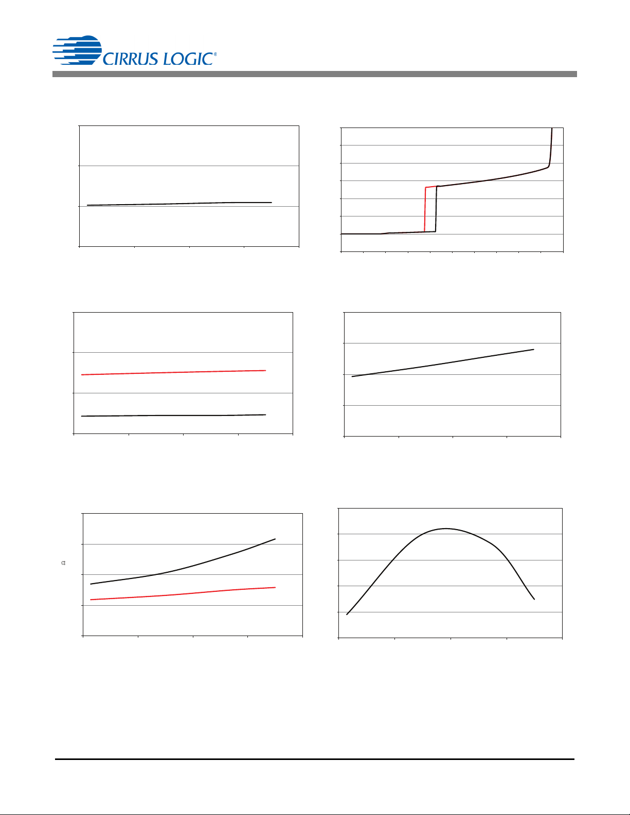
Figure 3. UVLO Characteristics
Figure 5. Turn-on/off Threshold Voltage vs. Temperature
Figure 4. Supply Current vs. Voltage
Figure 6. Zener Voltage vs. Temperature
Figure 7. Gate Drive Resistance vs. Temperature
DS954F3 11
Figure 8. Reference Current (I
) Drift vs. Temperature
ref
Page 12

5. GENERAL DESCRIPTION
5.1 Overview
The CS1630 and CS1631 are high-performance offline AC /DC
LED drivers for dimmable and high color rendering index (CRI)
LED replacement lamps and luminaires. They feature Cirrus
Logic’s proprietary digital dimmer compatibility control
technology and digital correlated color temperature (CCT) control
system that enables two-channel LED color mixing. The CS1630
is designed for 120VAC line voltage applications, and the
CS1631 is optimized for 230VAC line voltage applications.
The CS1630/31 integrates a critical conduction mode (CRM)
boost converter, providing power factor correction and superior
dimmer compatibility with a primary-side regulated quasiresonant second stage, which is configurable for isolated and
non-isolated topologies. The digital CCT control system provides
the ability to program dimming profiles, such as constant CCT
dimming and black body line dimming. The CS1630/31
optimizes LED color mixing by temperature compensating LED
current with an external negative temperature coefficient
(NTC) thermistor. The IC controller is also equipped with power
line calibration for remote system calibration and end-of-line
programming. The CS1630/31 provides a register lockout
feature for security against potential access to proprietary
registers.
5.2 Startup Circuit
An external, high-voltage source-follower circuit is used to
deliver startup current to the IC. During steady-state operation,
an auxiliary winding on the boost inductor biases this circuit to
an off state to improve system efficiency, and all IC supply
current is generated from the auxiliary winding. The patent
pending technology of the external, high-voltage sourcefollower circuit enables system compatibility with digital
dimmers (dimmers containing an internal power supply) by
providing a continuous path for a dimmer’s power supply to
recharge during its off state. During steady-state operation,
high-voltage FET Q1 is source-switched by a variable internal
current source on the SOURCE pin to create the boost circuit.
A Schottky diode with a forward voltage less than 0.6V is
recommended for diode D5. Schottky diode D5 will limit inrush
current through the internal diode, preventing damage to the IC.
5.3 Dimmer Switch Detection
The CS1630/ 31 dimmer switch detection algorithm determines
if the solid-state lighting system is controlled by a regular switch,
a leading-edge dimmer, or a trailing-edge dimmer. Dimmer
switch detection is implemented using two modes: Dimmer
Learn Mode and Dimmer Validate Mode. These assist in
limiting the system power losses. Once the IC reaches UVLO
start threshold V
in Dimmer Learn Mode, allowing the dimmer switch detection
and begins operating, the CS1630/31 is
ST(th)
CS1630/31
circuit to set the operating state of the IC to one of three modes:
No-dimmer Mode, Leading-edge Mode, or Trailing-edge Mode.
5.3.1 Dimmer Learn Mode
In Dimmer Learn Mode, the dimmer detection circuit spends
approximately two line-cycles learning whether there is a
dimmer switch and, if present, whether it is a trailing-edge or
leading-edge dimmer. A modified version of the leading-edge
algorithm is used. The trailing-side slope of the input line
voltage is sensed to decide whether the dimmer switch is a
trailing-edge dimmer. The dimmer detection circuit transitions to
Dimmer Validate Mode once the circuit detects that a dimmer is
present.
5.3.2 Dimmer Validate Mode
During normal operation, CS1630/31 is in Dimmer Validate
Mode. This instructs the dimmer detection circuit to periodically
validate that the IC is executing the correct algorithm for the
attached dimmer. The dimmer detection algorithm periodically
verifies the IC operating state as a protection against incorrect
detection. As additional protection, the output of the dimmer
detection algorithm is low-pass filtered to prevent noise or
transient events from changing the IC’s operating mode. The IC
will return to Dimmer Learn Mode when it has determined that
the wrong algorithm is being executed.
5.3.3 No-dimmer Mode
Upon detection that the line is not phase cut with a dimmer, the
CS1630/ 31 operates in No-dimmer Mode, where it provides a
power factor that is in excess of 0.9. The CS1630/31
accomplishes this by boosting in CRM and DCM mode. The
peak current is modulated to provide link regulation. The
CS1630/ 31 alternates between two settings of peak current. To
regulate the boost output voltage, the CS1630/31 uses a peak
current set by register PEAK_CUR (see "Peak Current
(PEAK_CUR) – Address 51" on page 39). The time that this
current is used is determined by an internal compensation loop
to regulate the boost output voltage. The internal algorithm will
reduce the peak current of the boost stage to maintain output
voltage regulation and obtain the desired power factor.
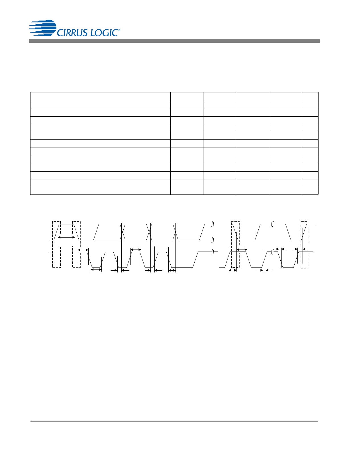
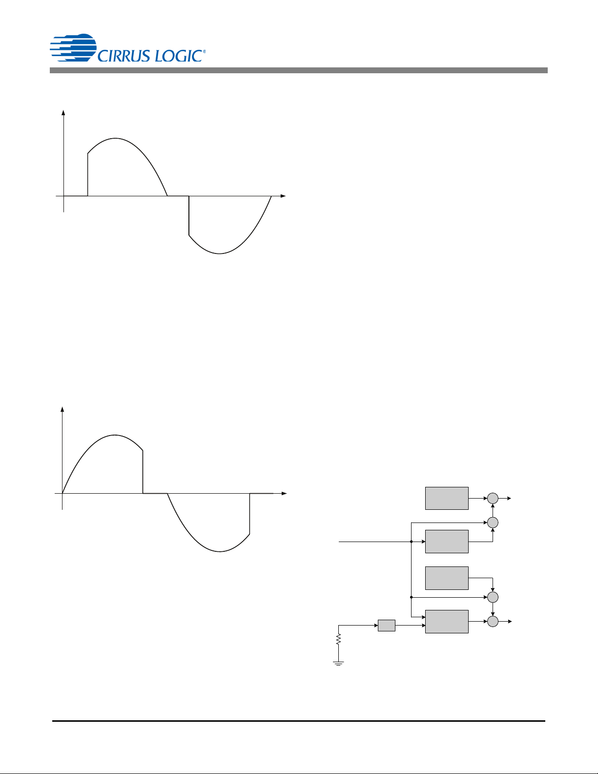
5.3.4 Leading-edge Mode
In Leading-edge Mode, the CS1630/31 regulates boost output
voltage V
Figure 9. on page 13). The device executes a CCM boost
algorithm using dimmer attach current as the initial peak current
for the initial firing event of the dimmer. Upon gaining control of
the incoming current, the CS1630/ 31 transitions to a CRM
boost algorithm to regulate boost output voltage V
device periodically executes a probe event on the incoming
while maintaining the dimmer phase angle (see
BST
BST
. The
12 DS954F3
Page 13
CS1630/31
Figure 9. Leading-edge Mode Phase-cut Waveform
Figure 10. Trailing-edge Mode Phase-cut Waveform
Gain
White
dim
I
White
I
ref
White
I
ref
Color
X
X
ADC
NTC
I
Color
Gain
Color
X
X
Figure 11. Block Diagram of Color Control System
waveform. The information from the probe event is used to
maintain proper operation with the dimmer circuitry.
5.3.5 Trailing-edge Mode
In Trailing-edge Mode, the CS1630/31 determines its operation
based on the falling edge of the input voltage waveform (see
Figure 10). To provide proper dimmer operation, the
CS1630/ 31 executes the boost algorithm on the falling edge of
the input line voltage that maintains a charge in the dimmer
capacitor. To ensure maximum compatibility with dimmer
components, the device boosts during this falling edge event
using a peak current that must meet a minimum value.
Trailing-edge Mode, only the CRM boost algorithm is used.
Red and amber LEDs are necessary components in
color-mixing applications when providing warm white or other
CCTs. When mixing colors, red and amber LEDs are the most
temperature sensitive, so they cause a large variation in
temperature. The CS1630/31 is capable of providing LED
CCT and luminosity with temperature compensation using the
NTC thermistor to resolve the significant change in the
luminous output due to temperature variations.
Since LED lumens are mainly a function of temperature and
forward current, color temperature and luminosity can be
maintained by independently adjusting each string's output
current as the ambient temperature changes. This can be
done by mapping the NTC reading to a required value of the
current in each string using a digital mapping block.
In the CS1630/31, only one of the LED string currents is
compensated for due to temperature variations. The current in
the other string is kept constant over temperature, which may
result in the luminosity decreasing slightly as temperature
increases. In order for the ADC to resolve the entire range of
possible temperature variation in the LEDs, it is recommended
to select series resistor R
and NTC resistor R
S
appropriate Beta value, which retains the total resistance
(RS+R
) at all possible operating temperatures within the
NTC
tracking range of the ADC. The final temperature-to-digital
code mapping depends on these variables.
The CS1630/31 color control system also has the ability to
maintain a constant CCT or change CCT as the light dims.
In
OTP configurations allow the selection of the dimming profile.
A specific CCT profile can be programmed to the digital
mapping device. In this case, the mapping is two-dimensional:
one current versus temperature profile is generated for each
dim level. The CS1630/31 provides two-dimensional mapping
for the color LED’s current only, and one-dimensional
mapping (current versus dim level) for the other string. A
simplified block diagram of the color control system is shown
in Figure 11.
NTC
with the
5.4 Correlated Color Temperature Control
The CS1630/31 color control system can adjust and maintain
the correlated color temperature (CCT) for the LED colormixing application by connecting an external negative
temperature coefficient (NTC) thermistor to the eOTP pin. The
LED temperature variation can be accurately detected by the
internal eOTP feedback loops
Protection" on page 19).
DS954F3 13
(see "External Overtemperature
Page 14

CS1630/31
where,
T = the measured normalized temperature and is 0 T 1.0
D = the normalized dim value and is 0
D1.0
GAIN
DTR
= gain of the channel based on the temperature measurement and the dim value:
where,
D = the normalized dim value and is 0
D1.0
GAIN
DR
= gain of the channel based on the dim value
GAIN
DTR
P30 T3 P20 T2 P10++T P03 D3 P02++D2 P01 D P21 T2D++= P12 T D2 P11 T D P00+++
[Eq.1]
GAIN
DR
Q3= D3 Q2 D2 Q1 D Q0+++
[Eq.2]
P
IN max
I
PKVRMS typ
2
------------------------------------------------
=
[Eq.3]
The reference currents are the required values at ambient
temperature TA= 25ºC and dim = 100%. They are multiplied
by the appropriate gains, and these values are passed to the
final power stage. The CS1630 / 31 uses polynomial
approximations in one and two dimensions to generate the
color gains. These polynomials can be up to third-order.
GAIN
compensation profile and dimming profile of the temperaturesensitive LEDs (see Equation 1). Profiles are programmed
through the Color Polynomial Coefficient registers (see "Color
Polynomial Coefficient (P30, P20, P10, P03, P02, P01, P21,
P12, P11, P00) – Address 5 - 24" on page 29).
GAIN
white LEDs (see Equation 2). The profile is programmed
through the Color Polynomial Coefficient registers (see "Color
Polynomial Coefficient (Q3, Q2, Q1, Q0) – Address 25 - 32" on
page 30).
Cirrus Logic, Inc. and its affiliates and subsidiaries generally
make no representations or warranties that the combination of
Cirrus Logic’s products with light-emitting diodes (“LEDs”),
converter materials, and/or other components will not infringe
any third-party patents, including any patents related to color
mixing in LED lighting applications, such as, for example, U.S.
Patent No. 7,213,940 and related patents of Cree, Inc. For
more information, please see Cirrus Logic’s Terms and
Conditions of Sale, or contact a Cirrus Logic sales
representative.
approximations create a custom temperature
DTR
approximation allows custom dimming profile of the
DR
5.5 Dimming Signal Extraction and the
5.6 Boost Stage
The high-voltage FET in the source-follower startup circuit is
source-switched by a variable current source on the SOURCE
pin to operate a boost circuit. Peak FET switching current is
set by the PEAK_CUR register (see "Peak Current
(PEAK_CUR) – Address 51" on page 39).
In No-dimmer Mode, the boost stage begins operating when
the start threshold is reached during each rectified half line-cycle and is disabled at the nominal boost output voltage. The
peak FET switching current determines the percentage of the
rectified input voltage conduction angle over which the boost
stage will operate. The control algorithm adjusts the peak FET
switching current to maximize the operating time of the boost
stage, thus improving the input power factor.
When operating in Leading-edge Mode, the boost stage
ensures the hold current requirement of the dimmer is met
from the initiation of each half-line dimmer conduction cycle
until the peak of the rectified input voltage. Trailing-edge Mode
boost stage ensures that the trailing-edge is exposed at the
correct time with the correct current.
5.6.1 Maximum Peak Current
The maximum boost inductor peak current is configured by
adjusting the peak switching current with peak current
code I
(PEAK_CUR) – Address 51" on page 39) is used to store peak
current code I
to peak current code I
. The PEAK_CUR register (see "Peak Current
PK(code)
. Maximum power output is proportional
PK(code)
, as shown in Equation 3:
PK(code)
Dim Mapping Algorithm
When operating with a dimmer, the dimming signal is
extracted in the time domain and is proportional to the
conduction angle of the dimmer. A control variable is passed
to the quasi-resonant second stage to achieve output currents
from 0% to 100%.
where,
= the correction term at 0.55
V
RMS(typ)
I
PK
= nominal operating input RMS voltage
= peak current code I
PK(code)
4.1mA
14 DS954F3
Page 15
CS1630/31
V
BST
CS1630 /31
15 k
ADC
R
BST
I
BSTOUT
I
ref
16
BSTOU T
R8
R9
Figure 12. BSTOUT Input Pin Model
R
BST
V
BST
I
ref
--------------
400V
133A
------------------
3M==
[Eq.4]
R3
R
IA C
I
AC
IAC
V
rect
CS1630 /31
15 k
ADC
R4
2
I
ref
12
Figure 13. IAC Input Pin Model
R
IAC
R
BST
=
[Eq.5]
5.6.2 Output BSTOUT Sense & Input IAC Sense
A current proportional to boost output voltage V
to the IC on pin BSTOUT and is used as a feedback control
signal (see Figure 12). The ADC is used to measure the
magnitude of current I
magnitude of current I
reference current I
Resistor R
BST
of 133A.
ref
sets the feedback current at the nominal boost
BSTOUT
through resistor R
BSTOUT
is then compared to an internal
output voltage. For 230VAC line voltage applications,
resistor R
is calculated as shown in Equation 4:
BST
where,
V
= nominal boost output voltage
BST
I
= internal reference current
ref
For 120VAC line voltage applications (CS1630), nominal
boost output voltage V
is 200V, and resistor R
BST
1.5M. By using digital loop compensation, the voltage
feedback signal does not require an external compensation
network.
A current proportional to the AC input voltage is supplied to the
IC on pin IAC and is used by the boost control algorithm (see
Figure 13).
is supplied
BST
BST
. The
BST
is
Resistor R
For optimal performance, resistors R
1% tolerance or better resistors for best V
sets current IAC and is derived from Equation 5:
IAC
IAC
and R
should use
BST
BST
voltage
accuracy.
5.6.3 Boost Auxiliary Winding
The boost auxiliary winding is used for zero-current detection
(ZCD). The voltage on the auxiliary winding is sensed through
the BSTAUX pin of the IC. It is also used to deliver startup
current during startup time (see "Startup Circuit" on page 12).
5.6.4 Boost Overvoltage Protection
The CS1630/31 supports boost overvoltage protection (BOP)
to protect the bulk capacitor C8 (see Figure 14. on page 16).
If the boost output voltage exceeds the overvoltage protection
thresholds programmed in the OTP registers a BOP fault
signal is generated. The voltage level, V
within 227V to 257V for a CS1630 and 432V to 462V for a
CS1631 (see "Configuration 53 (Config53) – Address 85" on
page 45). The control logic continuously averages the BOP
fault signal using a leaky integrator. When the output of the
leaky integrator exceeds a certain threshold, which can be set
using bits BOP_INTEG[3:0] in register Config53 (see
"Configuration 53 (Config53) – Address 85" on page 45), a
boost overvoltage fault is declared and the system stops
boosting. More information on the leaky integrator size and
sample rate is provided in section 6.23 "Configuration 18
(Config18) – Address 50" on page 38.
During a boost overvoltage protection event, the second stage
is kept enabled only if the MAX_CUR bit in register Config45
(see "Configuration 45 (Config45) – Address 77" on page 40)
is set to ‘1’ (enabled), and its dim input is railed to full scale.
This allows the second stage to quickly dissipate the stored
energy on the bulk capacitor C8, bringing down the boost
output voltage to a safe value. A visible flash on the LED might
appear, indicating that an overvoltage event has occurred.
When the boost output voltage drops to 195V (for a 120V
application), or 392V (for a 230V application), the boost stage
is enabled if bit BOP_RSTART in register Config54 (see
"Configuration 54 (Config54) – Address 86" on page 46) is set
to ‘1’, and the system returns to normal operation. If bit
BOP_RSTART is set to ‘0’, a boost overvoltage fault is latched
and the system stays in the fault mode until the input power is
recycled.
BOP(th)
, can be set
DS954F3 15
5.7 Voltage Clamp Circuit
To keep dimmers conducting and prevent them from misfiring,
a minimum power needs to be delivered from the dimmer to
the load. This power is nominally around 2W for 230 V and
120V TRIAC dimmers. At low dim angles (
power cannot be converted into light by the second stage due
to the dim mapping at light loads. The boost output
voltage V
can rise above the safe operating voltage of the
BST
primary-side bulk capacitor C8.
90°), this excess
Page 16
CS1630/31
CLAMP
Q3
R10
I
CLAMP
V
BST
S1
CS1630 /31
V
BE
VDD
3
C8
Figure 14. CLAMP Pin Model
D7
R13
Z2
R11
R14
Q4
CS1630/31
FBAUX
GND
13
GD
FBSENSE
15
12
11
T1
V
BST
R12
D9
C9
C11
C12
D11
D8
R15 D10
Q5
R16
C10
Z3
IGND
LED2 +
LED 1+
LED 1-
LED2 -
D
GND
_QVCC
Figure 15. Flyback Parallel Output Model
R13
R11
R14
Q4
L3
D8
CS1630 /31
FBAUX
GND
13
GD
FBSENSE
15
12
11
V
BST
R12
D9
C9
C11
C12
D11
R15 D10
Q5
R16
C10
Z3
IGND
LED 2+
LED1 +
LED 1-
LED 2-
D
GND
_QVCC
Figure 16. Buck Parallel Output Model
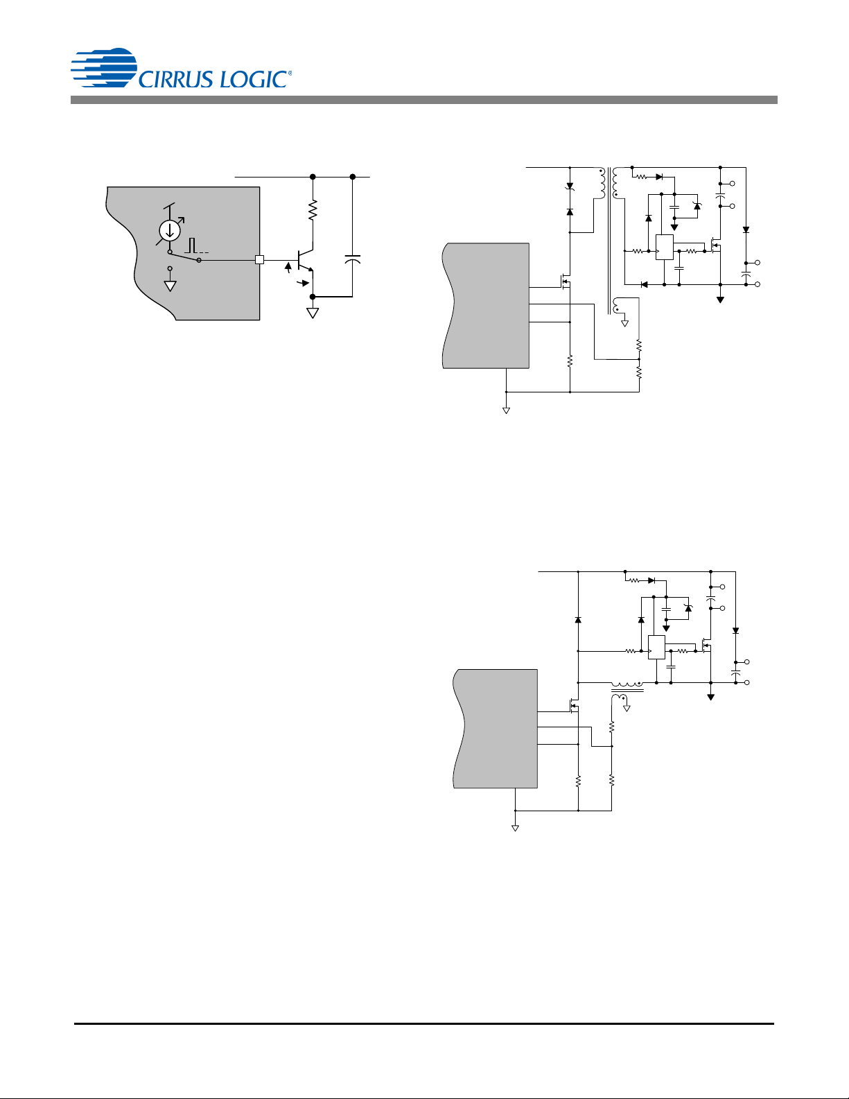
The CS1630/31 provides active clamp circuitry on the CLAMP
pin, as shown in Figure 14.
A PWM control loop ensures that the boost output
voltage V
does not exceed 227V for 120VAC applications
BST
or 424V for 230VAC applications. This control turns on the
BJT of the voltage clamp circuit, allowing the clamp circuit to
sink current through the load resistor, preventing boost output
voltage V
from exceeding the maximum safe voltage.
BST
5.7.1 Clamp Overpower Protection
The CS1630/31 clamp overpower protection (COP) control
logic continuously monitors the turn-on time of the clamp
circuit. If the cumulative turn-on time exceeds 84.48ms during
the internally generated 1 second window time, a COP event
is actuated, disabling the boost and second stages. The clamp
circuitry is turned off during the fault event.
Figure 15 illustrates a quasi-resonant flyback stage
configured for two-channel parallel output.
The flyback stage is controlled by measuring current in the
transformer primary and voltage on the auxiliary winding.
Quasi-resonant operation is achieved by detecting
transformer flyback using an auxiliary winding.
A quasi-resonant buck stage configured for two-channel
parallel output is illustrated in Figure 16.
5.8 Quasi-resonant Second Stage
The second stage is a quasi-resonant current-regulated DCDC converter capable of flyback, buck, or tapped buck
operation. The second stage output configuration is set by bit
S2CONFIG in register Config12 (see "Configuration 12
(Config12) – Address 44" on page 36) and bits BUCK[3:0] in
register Config10 (see "Configuration 10 (Config10) – Address
42" on page 35). To deliver the highest possible efficiency, the
second stage can operate in quasi-resonant mode and
provides constant output current with minimum line-frequency
ripple. Primary-side control is used to simplify system design
and reduce system cost and complexity.
The digital algorithm ensures monotonic dimming from 0 % to
100% of the dimming range with a linear relationship between
the dimming signal and the LED current.
16 DS954F3
Page 17
The buck stage is controlled by measuring current in the buck
R13
R11 R14
Q4
L3
CS1630 /31
FBAUX
GND
13
GD
FBSEN SE
15
12
11
D8
V
BST
R12
D9
C9
C11
C12
D11
R15 D10
Q5
R16
C10
Z3
IGND
LED2 +
LED1 +
LED1 -
LED 2-
D
GND
_QVCC
Figure 17. Tapped Buck Parallel Output Model
D7
R13
Z2
R11
R14
Q4
CS1630 /31
FBAUX
GND
13
GD
FBSENSE
15
12
11
T1
V
BST
R12
D9
C9
D8
R15 D10
R16
C10
Z3
D
GND
_QVCC
Q5
IGND
C12
LED 2+
LED2 -
C11
LED 1+
LED 1-
D11
Figure 18. Flyback Series Output Model
R13
R11 R14
Q4
L3
CS1630 /31
FBAUX
GND
13
GD
FBSENSE
15
12
11
V
BST
R12
D9
C9
R15 D10
R16
C10
Z3
D
GND
_QVCC
Q5
IGND
D11
D8
C12
LED1 +
LED1 -
C11
LED2 +
LED 2-
Figure 19. Buck Series Output Model
inductor and voltage on the auxiliary winding. Quasi-resonant
operation is achieved by detecting buck inductor
demagnetization using an auxiliary winding. The digital control
algorithm rejects line-frequency ripple created on the second
stage input by the front-end boost stage, resulting in the
highest possible LED efficiency and long LED life.
The tapped buck stage operates similar to a buck stage. The
tapped buck topology provides minimum turn-on time and
improves conversion efficiency when large input-to-output
voltage ratio is present. The tapped buck inductor behaves as
a transformer for voltage conversion and is controlled by
measuring current in the tapped inductor and voltage on the
auxiliary winding. Quasi-resonant operation is achieved by
detecting tapped inductor demagnetization using an auxiliary
winding.
CS1630/31
Similarly, a series connection in a flyback stage and buck
stage use an NMOS switch and a PMOS switch, respectively,
as shown in Figures 18 and 19.
5.8.1 Series & Parallel Two-Channel Output
The CS1630/31 is designed to be programmed to support
series or parallel two-channel output configurations using one
set of power magnetics. Series or parallel configuration is set
by bit STRING and bit LED_ARG in the Config3 register (see
"Configuration 3 (Config3) – Address 35" on page 32). A
parallel connection for a flyback stage and buck stage are
connected differently: an NMOS switch is used in flyback
configuration, and a PMOS switch is used in buck / tapped
buck configuration (see Figures 15, 16, and 17).
DS954F3 17
Page 18

CS1630/31
R13
R11
R14
Q4
L3
CS1630 /31
FBAUX
GND
13
GD
FBSEN SE
15
12
11
V
BST
R12
D9
C9
R15
D10
R16
C10
Z3
D
GND
_QVCC
Q5
IGND
C12
LED1 +
LED 1-
C11
LED 2+
LED 2-
D11
D8
Figure 20. Tapped Buck Series Output Model
CH1CUR
5112R
SenseICH1
NV
Sense
----------------------------------------------------------
= [Eq. 6]
CH2CUR
5112R
SenseICH2
NV
Sense
----------------------------------------------------------
= [Eq. 7]
Figure 20 illustrates the tapped buck stage configured for
series output mode.
To maintain constant output current with minimum linefrequency ripple, the following are required:
• For parallel configurations, a minimum voltage potential
difference between two strings
• For series configurations, a minimum current amplitude
difference between two strings
5.8.2 Primary-side Current Control for Two-Channel Output
The CS1630/31 regulates two-channel output current
independently using primary-side control, which eliminates
the need for opto-coupler feedback. The control loop operates
in peak current control mode, with the peak current set cycleby-cycle by the two independent current regulation loops.
Demagnetization time of the second stage inductor is sensed
by the FBAUX pin using an auxiliary winding on the second
stage inductor. The FBAUX pin supplies an input to the digital
control loop.
The power conversion for two-channel output is carried out by
interleaving the PWM. The two-channel control system
consists of two components:
• A toggle device (phase synchronizer circuit) on the
secondary side that alternatively activates each output
channel for each switching event
• A digital sequencer on the primary side determines which
output channel is active for any given switching event
As the output is toggled between each channel, a sequencer
on the primary side identifies the current control phase and
regulates the current in each output channel. To ensure
proper operation for a parallel configuration, the two output
channels should target a voltage differential that is greater
than 20%. For a series configuration, the two output channels
should target a current differential that is greater than 20%.
18 DS954F3
5.8.3 Auxiliary Winding Configuration
The second-stage inductor auxiliary winding is used for zerocurrent detection (ZCD) and overvoltage protection (OVP). The
auxiliary winding is sensed through the FBAUX pin of the IC.
5.8.4 Control Parameters
The second-stage control parameters are set to assure:
• Line Regulation — The LED current remains constant
despite a ±10% AC line voltage variation.
• Effect of Variation in Transformer Magnetizing
Inductance — The LED current remains constant over
a ±20% variation in magnetizing inductance.
The FBSENSE input is used to sense the current in the
second stage inductor. When this current reaches a certain
threshold, the gate drive turns off (output on pin GD).
Two OTP values are required to set the second-stage output
currents, CH1CUR for channel 1 and CH2CUR for channel 2
(see "Channel 1 Output Current (CH1CUR) – Address 41" on
page 35 and "Channel 2 Output Current (CH2CUR) – Address
43" on page 35). Equations 6 and 7 are used to calculate the
values to be programmed into registers CH1CUR and
CH2CUR.
where,
= resistance of current sense resistor
R
Sense
V
= full scale voltage across sense resistor (~1.4V)
Sense
I
= target current in channel 1 LED string
CH1
I
= target current in channel 2 LED string
CH2
Sense resistor R
is determined by the input voltage,
Sense
switching frequency, auxiliary transformer turns ratio, target
output current and output voltage for each channel.
The zero-current detect input on pin FBAUX is used to
determine the demagnetization cycle period T2 . The controller
then uses these inputs to control the gate drive output pin GD.
5.8.5 Frequency Dithering
The peak amplitude of switching harmonics can be reduced by
spreading the energy into wider spectrums. The frequency
dithering level can be managed using bits DITLEVEL[1:0] in
register Config61 (see "Configuration 61 (Config61) – Address
93" on page 49). Additionally, the CS1630/31 has an option to
enable dithering only in No-dimmer Mode by setting bit
DITNODIM to ‘1’. If output currents differ, the CS1630/31 also
has an option to allow for less dither on one of the two
channels by selecting the channel using bit DITCHAN. The
channel selected for less dither attenuates the dither level by
the percentage configured by bits DITATT[1:0].
Page 19

CS1630/31
5.8.6 Output Open Circuit Protection
Output open circuit protection and output overvoltage
protection (OVP) are implemented by monitoring the output
voltage through the second-stage inductor auxiliary winding.
Overvoltage protection is enabled by setting bit OVP to ‘0’ in
register Config47 (see "Configuration 47 (Config47) – Address
79" on page 41). If the voltage on the FBAUX pin exceeds a
threshold (V
gate drive is turned off and outside of the blanking window
configured by bit OVP_TYPE and bits OVP_BLANK[2:0] in
register Config50 (see "Configuration 50 (Config50) – Address
82" on page 43), then the OVP event accumulator is
incremented by 1 before the start of the next switching cycle.
If the OVP comparator threshold is not exceeded during the
switching cycle, the event accumulator is decremented by 1. If
the event accumulator count exceeds or equals the count set
by bits OVP_CNT[2:0] in register Config50 then an OVP fault
is declared and enters a fault state.
The fault state is latched if bit OVP_LAT in register Config50
is set high. The OVP fault state is not cleared until the power
to the IC is recycled. Otherwise, if bit OVP_LAT is set low, the
system is restarted after a specified amount of time configured
by using the bit FAULT_SLOW and bits RESTART[5:0] in
register Config51 (see "Configuration 51 (Config51) – Address
83" on page 43). The fault behavior during the fault state
initiated by this protection depends on the setting for bit
FAULT_SHDN in register Config51.
) of 1.25V during the time the second stage
OVP(th)
5.8.7 Overcurrent Protection
Overcurrent protection (OCP) is implemented by monitoring
the voltage across the second-stage sense resistor.
Overcurrent protection is enabled by setting bit OCP to ‘0’ in
register Config47 (see "Configuration 47 (Config47) – Address
79" on page 41). If this voltage exceeds a threshold (V
of 1.69V during the time the second stage gate drive is turned
on’ and outside of the blanking window configured by bits
OCP_BLANK[2:0] in register Config48 (see "Configuration 48
(Config48) – Address 80" on page 42), then the OCP event
accumulator is incremented by 1 after the gate drive turns off.
If the OCP comparator threshold is not exceeded during this
time, the event accumulator is decremented by 1. If the event
accumulator count exceeds or equals the count set by bits
OCP_CNT[2:0] in register Config49 (see "Configuration 49
(Config49) – Address 81" on page 42) then an OCP fault is
declared and enters a fault state.
The fault state is latched if bit OCP_LAT in register Config49
is set high. The OCP fault state is not cleared until the power
to the IC is recycled. Otherwise, if bit OCP_LAT is set low, the
system is restarted after a specified amount of time configured
by using the bit FAULT_SLOW and bits RESTART[5:0] in
register Config51 (see "Configuration 51 (Config51) – Address
83" on page 43). The fault behavior during the fault state
initiated by this protection depends on the setting for bit
FAULT_SHDN in register Config51.
OCP(th)
5.8.8 Open Loop Protection
Open loop protection (OLP) and sense resistor short
protection are implemented by monitoring the voltage across
the sense resistor. Open loop protection is enabled by setting
bit OLP to ‘0’ in register Config47 (see "Configuration 47
(Config47) – Address 79" on page 41). If the voltage on pin
FBSENSE does not reach the protection threshold
voltage V
the second stage gate drive is turned on and the blanking
window configured by bits OLP_BLANK[2:0] in register
Config48 (see "Configuration 48 (Config48) – Address 80" on
page 42) has elapsed, then the OLP event accumulator is
incremented by 1. If the OLP comparator threshold is
exceeded during this time, the event accumulator is
decremented by 1. If the event accumulator count exceeds or
equals the count set by bits OLP_CNT[2:0] in register
Config49 (see "Configuration 49 (Config49) – Address 81" on
page 42) then an OLP fault is declared and enters a fault
state.
The fault state is latched if bit OCP_LAT in register Config49
is set high. The OLP fault state is not cleared until the power
to the IC is recycled. Otherwise, if bit OLP_LAT is set low, the
system is restarted after a specified amount of time configured
by using the bit FAULT_SLOW and bits RESTART[5:0] in
register Config51 (see "Configuration 51 (Config51) – Address
83" on page 43). The fault behavior during the fault state
initiated by this protection depends on the setting for bit
FAULT_SHDN in register Config51.
of 200mV during a 250ns scan period after
OLP(th)
5.9 Overtemperature Protection
The CS1630/31 incorporates an internal overtemperature
protection (iOTP) circuit for IC protection and the circuitry
required to connect an external overtemperature protection
)
(eOTP) device. Typically, a negative temperature coefficient
(NTC) thermistor is used.
5.9.1 Internal Overtemperature Protection
Internal overtemperature protection (iOTP) is activated and
power switching devices are disabled when the die
temperature of the CS1630/31 exceeds 135 °C. A hysteresis
of about 7°C occurs before resuming normal operation.
5.9.2 External Overtemperature Protection
The external overtemperature protection (eOTP) pin is used to
implement overtemperature protection using an external NTC
thermistor R
converted to an 8-bit digital ‘CODE’ (which gives an indication
of the temperature) using a digital feedback loop that adjusts
the current I
resistor R
(V
CONNECT(th)
. The total resistance on the eOTP pin is
NTC
CONNECT
to maintain a constant reference voltage of 1.25V
S
into the NTC thermistor R
).
NTC
and series
DS954F3 19
Page 20

CS1630/31
CS1630/31
+
-
I
CONNECT
V
CONNECT (th)
Comp_Out
eOTP
Control
eOTP
R
S
C
NTC
NTC
V
DD
10
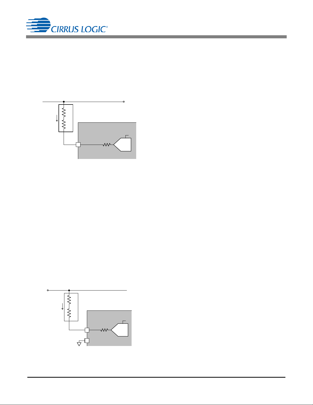
Figure 21. eOTP Functional Diagram
I
CONNECT
V
CONNECT th
R
-------------------------------------
=
[Eq.8]
CODE
I
CONNECT
2
N
---------------------------
V
CONNECT th
R
NTCRS
+
-------------------------------------
=
[Eq.9]
CODE
2NV
CONNECT th
I
CONNECTRNTCRS
+
-----------------------------------------------------------------
=
[Eq.10]
4M
R
NTCRS
+
---------------------------------
=
256 1.25 V
80AR
NTCRS
+
----------------------------------------------------------
=
Figure 21 illustrates the functional block diagram when
connecting an optional external NTC temperature sensor to
the eOTP circuit.
Current I
CONNECT
is generated from an 8-bit controlled current
source with a full-scale current of 80A. See Equation 8:
When the loop is in equilibrium, the voltage on the eOTP pin
fluctuates around threshold voltage V
digital ‘CODE’ output by the ADC is used to generate
current I
current I
CONNECT
CONNECT
. In normal operating mode,
is updated once every seventh half
line-cycle by a single ± LSB step. See Equation 9:
Use Equation 9 to solve for the 8-bit digital CODE output.
See Equation 10:
The tracking range of this ADC is approximately 15.5 k to
4M. The series resistor R
of the NTC thermistor R
range so that the entire 8-bit dynamic range of the ADC is well
used. A 14k (±1% tolerance) series resistor is required to
allow measurements of up to 130°C to be within the eOTP
tracking range when using a 100k NTC thermistor with a
Beta of 4334. The eOTP tracking circuit is designed to function
accurately with an external capacitance of a maximum of
470 pF. A higher 8-bit code output reflects a lower resistance
and hence a higher external temperature.
20 DS954F3
CONNECT(th)
is used to adjust the resistance
S
to fall within this ADC tracking
NTC
. The 8-bit
The ADC output code is filtered to suppress noise. This filter
is the faster low-pass filter with a programmable time constant
configured using bits EOTP_FLP[2:0] in register Config55
(see "Configuration 55 (Config55) – Address 87" on page 47)
and compared against a programmable code value that
corresponds to the desired shutoff temperature set point.
Shutoff temperature Temp
Shutdown
is set using bits
SHUTDWN[3:0] in register Config58 (see "Configuration 58
(Config58) – Address 90" on page 48). If the temperature
exceeds this threshold, the chip enters an external
overtemperature state and shuts down. The external
overtemperature state is not a latched protection state, and
the ADC keeps tracking the temperature in this state in order
to clear the fault state once the temperature drops below a
temperature code corresponding to temperature Temp
Wakeup
programmed using bits WAKEUP[3:0] in register Config46
(see "Configuration 46 (Config46) – Address 78" on page 40).
When exiting reset, the chip enters startup and the ADC
quickly (<5ms) tracks the external temperature to check if it is
below the temperature Temp
(CODE
) before the boost and second stages are
Wakeup
reference code
Wakeup
powered up. If this check fails, the chip will wait until this
condition becomes true before initializing the rest of the
system.
For external overtemperature protection, a second low-pass
filter with a programmable time constant of 2 minutes is
configured using bits EOTP_SLP[2:0] in register Config55
(see "Configuration 55 (Config55) – Address 87" on page 47).
The filter is applied to the ADC output and uses it to scale
down the internal dim level of the system (and hence
current I
threshold that corresponds to temperature Temp
) if the temperature exceeds a programmable 8-bit
LED
eOTP
(see
Figure 22. on page 21). The large time constant for this filter
ensures that the dim scaling does not happen spontaneously
(suppress spurious glitches) and is not noticeable.
Temperature thresholds must be set such that
eOTP
<Temp
Temp
sets temperature Temp
Wakeup
<Temp
eOTP
Shutdown
. Register Config59
(see "Configuration 59
(Config59) – Address 91" on page 48). Register Config46 sets
temperature Temp
(see "Configuration 46 (Config46) –
Wakeup
Address 78" on page 40). Register Config58 sets temperature
Temp
Shutdown
(see "Configuration 58 (Config58) – Address
90" on page 48).
For example, the system can be set up such that current I
starts reducing when thermistor R
is approximately 6.3k
NTC
(assuming a 14k1% tolerance, series resistor R
), which
S
LED
corresponds to a temperature of 95°C (temperature
Temp
(100 kW at 25°C). The I
code is 196) for a 100k NTC with a Beta of 4334
eOTP
current is scaled based on the
LED
programmed slope using bits RATE[1:0] in register Config44
(see "Configuration 44 (Config44) – Address 76" on page 39)
until it reaches temperature Temp
Shutdown
uses this calculated value to scale output LED current I
. The CS1630/31
, as
LED
shown in Figure 22. on page 21.
Page 21

Beyond this temperature, the IC shuts down using the
Temperature (°C)
Cu rr e nt (I
LED
, Nom.)
125
95
50%
100%
0
25
eOTP Tr ips and
Shuts O ff Lam p
Figure 22. LED Current vs. eOTP Temperature
Power Supply
LED Lamp
with
CS1630/31
Photode tec tor
Light
Measurement
Light
Calibrat or
Line
Neutral
Figure 23. Power Line Calibration Block Diagram
mechanism discussed above.
If the external overtemperature protection and the
temperature compensation for CCT control features are not
required, connect the eOTP pin to GND using a 50k to
500k resistor to disable the eOTP feature so that the
programmed temperatures Temp
Wakeup
and Temp
Shutdown
codes are greater than the measured 8-bit code
corresponding to the total resistance on pin eOTP.
5.10 Power Line Calibration
The CS1630/31 integrates power line calibration technology
within the controller to enable calibration and end-of-line
programming without the need for an additional electrical
connection, as shown in Figure 23.
CS1630/31
The power line calibration uses a phase-cut mechanism for
data generation and return-to-zero data encoding to eliminate
the need for clock synchronization. A code / command can be
created by using the combination of input phase angles, as
detailed in "Power Line Calibration Characteristics" on page 9.
When an initial program mode command has been detected,
the controller will begin to enter calibration mode. After key
parameters of the lighting system have been characterized
and programmed, a burn-in code plus an end-program mode
command is transmitted, instructing the controller to exit the
calibration mode. Power line calibration and end-of-line
programming requires no human intervention. The
CS1630/31 provides registers that allow up to three attempts
for LED output current trimming over power line calibration.
Six registers store the three optional color control system
calibration values for channel 1 color calibration and channel
2 color calibration. For more detail regarding color calibration,
see "Channel 1 Color Calibration 3A (CH1_CAL3A) – Address
119" on page 51 through "Channel 2 Color Calibration 3C
(CH2_CAL3C) – Address 126" on page 53.
5.10.1 Power Line Calibration Specification
To ensure the success of phase detection, the angle for each
bit is specified as shown in "Power Line Calibration
Characteristics" on page 9. The CS1630/31 power line
calibration system operates under universal line voltage and
frequency with a leading-edge, phase-cut waveform.
DS954F3 21
Page 22

5.10.2 PLC Program Mode Characters
90°
Special Char
‘11’
146°
‘01’
62°
‘10’
118°
‘00’
34°
90° 146° 90°
PLC Stop Char
90° 34° 90°
PLC Start Char
Figure 24. Power Line Calibration Mode Character Waveforms
PLC Start Character
Addr Bcast
&
Simple Code
00
PLC Operation Code
(4-bit)
0000
Odd Parity
&
Don’t Care
10
PLC Stop Character
Before Transmit
After Transmit
135° 135° 135° 135°90° 34° 90° 90° 146° 90°34° 34° 118°34°
Figure 25. Power Line Calibration Mode Example
Calibration Command Sequence
Start Char [(SC)00(SC)] Addr Bcast
&
Simple Code
[1 Duo-bit]
OPCODE
[2 Duo-bits]
Odd Parity
&
Don’t Care
[1 Duo-bit]
Stop Char [(SC)11(SC)]
In order to program the CS1630/31, a set of encoded
characters is built from specific phase-cut waveform patterns.
Figure 24 illustrates the phase-cut waveform encoding
recognized by the CS1630/31 power line calibration system.
As shown in Table 1, six characters are formed using the
special character and two-bit encoded data.
Character Code Notes
Start Char (SC)00(SC) PLC Program Start Character
Stop Char (SC)11(SC) PLC Program Stop Character
Duo-bit ‘00’ 00 2-bit Data [00]
Duo-bit ‘01’ 01 2-bit Data [01]
Duo-bit ‘10’ 10 2-bit Data [10]
Duo bit ‘11’ 11 2-bit Data [11]
Note: (1) A Special Character (SC) must precede and follow the Duo-bit.
(1)
(1)
Table 1. Power Line Calibration Characters
5.10.3 Calibration Mode Operation Code
The CS1630/31 power line calibration system requires a start
and stop operation code to activate and deactivate power line
calibration mode. Once in the power line calibration mode,
operation codes (OPCODE) will be used to program specific
addresses using the OPCODE listed in Table 2.
CS1630/31
Name OPCODE Description
NOP 0000 No Operation
INIT_PROG_MODE 0001 Initialize program mode
I2C_WRITE 0010 Perform a generic I2C write
0011 Reserved
BURN_OTP 0100 Initiate an OTP write cycle
STR1_OFFSET 0101 Write String 1 offset
STR2_OFFSET 0110 Write String 2 offset
WRITE_CRC 0111 Write CRC value
END_PROG_MODE 1000 Disable programming mode
WRITE_DIM 1001 Sets PLC dim value
Notes: (1) Allows other commands to program the device under test.
(2) Range of Offset tolerance is ±15 %.
(3) The light is flashed to indicate pass or fail.
Table 2. Power Line Calibration Operation Code
The LED light flashes seven times to indicate a command
error. The LED flashes two times when OTP registers are
programmed successfully and four times when programming
is unsuccessful. Figure 25 illustrates an example of a power
line calibration mode command sequence and the cutwaveform pattern.
(1)
(3)
(2)
(2)
22 DS954F3
Page 23

CS1630/31
CRC CRC x8x2x1+++=
[Eq.11]
01238
Figure 27. I2C Frame Format
‘1’ = Block
‘0’ = Single
PADataS A A
Device Address
(7-bit)
Register Address
(7-Bit)
Data
… ...
From Slave to Master
From Master to Slave
BLK/ SGLR/ W
‘1’ = Read
‘0’ = Write
Star t
Cond ition
Stop
Condition
‘A’ = Acknowledge (SDA Low)
A = Not Acknowledge (SDA High)
‘’
A/A A/ A
Data Transferred
(n bytes and acknowledge)
A/A A/A
Slave Address
(1 byte and acknowledge)
5.10.4 Register Lockout
The CS1630/31 provides register lockout for security against
unauthorized access to proprietary registers using the I
PLC communication port. A 32-bit long-word is used for
password protection when accessing the OTP registers. The
register lockout password can be set by programming the
Lockout Key registers (see "Lockout Key (LOCK0, LOCK1,
LOCK2, LOCK3) – Address 1 - 4" on page 29). Register
lockout is enabled by setting bit LOCKOUT in register Config0
(see "Configuration 0 (Config0) – Address 0" on page 29).
2
C or
5.11 I2C™ Communication Interface
The purpose of the communication system is to provide a
mechanism to allow the transfer of data and accessibility to
the device. Pins SDA and SCL are an I
used to provide access to control registers inside the EXL
core. In applications that do not use I
SDA and SCL should be connected to VDD. When SDA and
SCL are connected to VDD, read/write register values are
controlled internally by the EXL core.
A one-time programmable (OTP) memory is implemented as
part of the communication system to store trim and key
parameters. After power-on reset (POR), the OTP memory is
uploaded into shadow registers as part of startup, and a cyclic
redundancy check (CRC) is calculated and checked on the
data read from the OTP memory. If the computed CRC does
not match the CRC value saved in the OTP memory, default
values are used for some of the parameters. Shadow registers
can be written using the I
2
C interface. In order to write to or
read from the I2C port, a defined messaging protocol must be
implemented.
The OTP memory is organized as 128 addressable bytes (8
bits). The contents of the OTP memory are read at reset and
are addressable by the I
2
C interface. The shadow register
values are used to control the internal operational parameters
of the IC and can be modified. However, in the event of a POR
or any kind of reset, the shadow registers will be rewritten with
the OTP memory content. In the event that a CRC verification
fails during normal operation, the registers will be rewritten
with OTP memory content, negating any changes that have
been made to the shadow registers.
The CRC is verified after the OTP memory has been uploaded
at POR, periodically during the operation of the IC, and at the
2
C communication port
2
C communication, pins
exit of Control Port mode. The CRC can be disabled by writing
to the CRC disable register, or by enabling the Control Port
mode (see "Control Port Enable" on page 24). The shadow
registers will be restored from OTP memory on a POR event,
or any reset type event. The CRC is calculated using
Equation 11.
The CRC calculation is implemented in hardware using a
linear feedback shift register starting with address 0 and
ending with address 57 (see Figure 26). The current CRC is
stored in address 63.
Figure 26. CRC Hardware Representation
To perform a successful write to the OTP memory, the CRC
must be calculated and stored in the CRC registers prior to
issuing the OTP write command. OTP memory can only be
written once. OTP shadow registers accessible to the user are
described in "One-Time Programmable (OTP) Registers" on
page 27.
5.11.1 I2C Control Port Protocol
The communication port is designed to allow a master device
to read and write the OTP shadow registers of the CS1630/31
and the capability of programming the OTP memory using the
data in the shadow registers. The OTP shadow registers
provide a mechanism for configuring the device and
calibrating the system prior to programming the device. The
CS1630/31 communication port physical layer adheres to the
2
C bus specification by Philips Semiconductor version 2.1,
I
January 2000 (see "I
page 8). The CS1630/31 control port only supports I2C slave
functionality. The CS1630/31 I
with a single master and no other slaves on the bus.
Figure 27 illustrates the frame format used for I
transfers. The first bit is a Start condition (bit S) followed by an
8-bit slave address that is comprised of a 7-bit device address
plus a Read/Write
significant bit of the slave address byte, which indicates
2
C™ Port Switching Characteristics" on
2
C interface is intended for use
2
C data
(R/W) bit. The R/W bit is the least
DS954F3 23
Page 24

CS1630/31
Figure 28. Frame Formats for Read Operation
0A0S A
Device A ddr ess
(7-bit)
Register Address
(7-bit)
‘0’ = Single
‘0’ = WriteStart
Cond ition
Stop
Cond ition
Data Transferred
(1 Byte and Acknowledge)
Slave Addr ess
(1 Byte and Acknowledge)
PAData
‘A’ = Acknowledg e
(SDA Low)
‘1’ = Block
S A
Device Address
(7-Bit)
Register Addr ess
(7-Bit)
Data
… ...
From Slave to Master
From Master to Slave
‘0’ = Wr iteStart
Condition
Stop
Cond ition
Data Transferred
(n Bytes and Acknowledge)
0 A 1 A
Slave Address
(1 Byte and Acknowledge)
PAData
Data
Data
A1S
Device Address
(7-bit)
‘1’ = Read
Slave Addr ess
(1 Byte and Acknowledge)
S
Device Addr ess
(7-Bit)
‘1’ = Read
1 A
Slave Address
(1 Byte and Acknowledge)
‘A’ = Acknowledg e
(SDA Low)
whether data transfer is a read or write operation. This bit
should be set to '0' to perform a write operation and '1' to
perform a read operation. The 7-bit device address is the 7
most significant bit of the slave address. For data transfers,
the CS1630/31 acknowledges a binary device address of
‘0010000’, which is reserved for accessing OTP shadow
registers (see "One-Time Programmable (OTP) Registers" on
page 27).
After the 7-bit device address is received, the Control Port
performs a compare to determine if it matches the CS1630/31
device address. If the compare is true, the Control Port will
respond with an Acknowledge (bit A) and prepares the device
for a read or write operation. The final bit is the Stop condition
(bit P), which is sent by the master to finish a data transfer.
The communication port supports single and block data
transfers. The block read or write capability is available by
setting the MSB of the register address to ‘1’. Device address
0x10 provides access to the OTP shadow registers in the
address range of 0x00 to 0x7F.
5.11.2 Control Port Enable
Control Port mode is enabled and initiated by transmitting a
two-byte hardware pass code using an I
To enable the control port, the master needs to write a Start
condition followed by a slave address of 0x22 (7 MSB device
address = ‘0010001’ and the LSB R/W = ‘0’ for a write
operation). Then a 0x81 (MSB BLK/SGL = ‘1’ and 7 LSB
register address = ‘0000001’) followed by two bytes of data
0xF4 and 0x4F, ending the transmission with a Stop condition.
Once in Control Port mode, the CS1630/31 can be configured
to perform color calibration functions and program the OTP
memory. Several other system configuration tasks can be
performed by writing and reading the shadow registers using
2
C port.
the I
2
C block write.
5.11.3 Read Operation
To enter a read operation, the master must set up the Control
Port by writing a Start condition, the 7-bit device address, the
R/W
bit, the Block/Single (BLK/SGL) bit, and the 7-bit shadow
register address. The master can then perform a read
operation to retrieve the required bytes from the shadow
registers. Figure 28 illustrates the protocol for a single and
block read operation.
To perform a single shadow register read, a write to the
Control Port must be used to set up the shadow register
address and the BLK/SGL
configuration bit (indicating a single
read operation). To enter a single read operation, a Start
condition followed by a slave address of 0x20 (7 MSB device
address = ‘0010000’ and the LSB R/W
= ‘0’ for a write
operation) is sent at the start of the message. The MSB of the
second byte is cleared to ‘0’ to indicate a single byte read. The
remaining 7 bits of the second byte represent the shadow
register address of the read operation. To perform the single
read operation, a Start condition followed by a slave address
of 0x21 (7 MSB device address = ‘0010000’ and the LSB
= ‘1’ for a read operation) is sent at the start of the
R/W
operation. After receiving the byte of data, the master should
terminate the message by sending a Not Acknowledge
followed by a Stop condition. The protocol for a single read
operation is illustrated by the top frame in Figure 28.
To enter a block read operation, the master must set up the
Control Port by writing a Start condition followed by a slave
address of 0x20 (7 MSB device address = ‘0010000’ and the
LSB R/W
= ‘0’ for a write operation) at the start of the
message. The MSB of the second byte is set to ‘1’ to indicate
a block read. The remaining 7 bits of the second byte
represent the starting shadow register address of the read
operation. To perform the block read operation, a Start
condition followed by a slave address of 0x21 (7 MSB device
address = ‘0010000’ and the LSB R/W
= ‘1’ for a read
operation) is sent at the start of the operation. The slave
continues to send data bytes until the master sends a Not
Acknowledge followed by a Stop condition, signifying the end
of the block read operation. The protocol for a block read
operation is illustrated by the bottom frame in Figure 28.
24 DS954F3
Page 25

CS1630/31
Figure 29. Frame Formats for Write Operation
0A0S A
Device Address
(7-bit)
Register Address
(7-bit)
‘0’ = Single
‘0’ = Wr iteStart
Condition
Stop
Condition
Data Transferr ed
(1 Byte and Acknow ledge )
Slave Address
(1 Byte and Acknowledge)
PAData
‘A’ = Acknowledge
(SDA Low)
‘1’ = Block
S A
Device Address
(7-Bit)
Register Address
(7-Bit)
Data
… ...
From Slave to Master
From Master to Slave
‘0’ = Wr iteStart
Cond ition
Stop
Condition
‘A’ = Acknowledge (SDA Low)
Data Transferred
(n Bytes and Acknowledge )
0 A 1 A
Slave Address
(1 Byte and Acknowledge)
PAData
5.11.4 Write Operation
To perform a write operation, the master must write the 7-bit
device address, the R/W
shadow register address. The master can then write the
required bytes to the shadow registers. Figure 29 illustrates
protocol for a single and block write operation.
To perform a single shadow register write, a write to the
Control Port must be used to set up the shadow register
address and the BLK/SGL
write operation). To initiate a single write operation, a Start
condition followed by a slave address of 0x20 (7 MSB device
address = ‘0010000’ and the LSB R/W
operation) is sent at the start of the message. The most
significant bit of the second byte is cleared to ‘0’ to indicate a
single byte write. The remaining 7 bits of the second byte
represent the shadow register address of the write operation.
After receiving the Acknowledge from the Control Port, the
master should terminate the message by sending a Stop
condition. The protocol for a single write operation is shown as
the top frame in Figure 29.
To initiate a block write operation, a Start condition followed by
a slave address of 0x20 (7 MSB device address =
‘0010000’and the LSB R/W
at the start of the message. The MSB of the second byte is set
to ‘1’ to indicate a block write. The remaining 7 bits of the
second byte represent the starting shadow register address of
the write operation. The slave continues to send data bytes
until the master sends a Stop condition after receiving the
Acknowledge, signifying the end of the block write message.
The protocol for a block write operation is illustrated by the
bottom frame in Figure 29. Block writes will wrap around from
shadow register address 127 to 0 if a Stop condition is not
received.
bit, the BLK/SGL bit, and the 7-bit
configuration bit (indicating a single
= ‘0’ for a write
= ‘0’ for a write operation) is sent
5.11.5 Customer I2C Lockout
The CS1630/31 provides a mechanism that locks or disables
the I2C control port. This feature provides security against
potential access to proprietary register settings and OTP
memory (color compensation) through the I
enable the lockout feature, the LOCKOUT bit is set to ‘1’ in the
Config0 register (see "Configuration 0 (Config0) – Address 0"
on page 29) and setting a 32-bit Lockout Key in registers
LOCK3, LOCK2, LOCK1, and LOCK0 (at register address
0x01 to 0x04). The value of the Lockout Key is user
programmable and stored in OTP memory (see "Lockout Key
(LOCK0, LOCK1, LOCK2, LOCK3) – Address 1 - 4" on
page 29).
To unlock the Control Port, the proper programmed Lockout
Key is written to the 32-bit Lockout Key shadow registers
LOCK3, LOCK2, LOCK1, and LOCK0. The Lockout Key must
be written in ascending address order for the lockout to be
disabled. The MODE bit in register Config0 is set to ‘1’, the
Color Polynomial Coefficient registers P10_MSB, P10_LSB,
P01_MSB, and P01_LSB (at register address 0x09, 0x0A,
0x0F, and 0x10) are appended to the Lockout Key to increase
security. If the wrong Lockout Key is written to the shadow
resisters when attempting to disable the lockout feature, the
part cannot be unlocked until a reset cycle occurs.
In lockout mode, the Control Port disables the following
operations through the I
2
•I
C read operations from OTP shadow registers (value
2
C communication port:
of 0x0 will be read through control port)
2
C write operations to lockout enabled or key shadow
•I
registers (including read operations through PLC)
• Direct OTP memory read or write (including reads/writes
through PLC)
Write operations to either OTP or test space (except OTP
Lockout Key) are allowed in lockout mode.
2
C control port. To
DS954F3 25
Page 26

CS1630/31
5.12 OTP Memory
At startup, the contents of the OTP memory are read into
shadow registers that make up a register file. Access to the
OTP memory values is accomplished by reading and writing
to the OTP corresponding address locations in that register
file. To program the part, each unprogrammed address
location must be filled with an appropriate value. Next, a CRC
is calculated corresponding to the OTP space that is being
programmed. Lastly, two special registers are written to
initiate a burn/program cycle.
5.12.1 Programming the OTP Memory
When the CS1630/31 is shipped, some of the OTP memory
will already be programmed. Do not clear any bits to ‘0’ that
are programmed to '1', and do not modify any registers or bits
that are reserved. Changing bits from '1' to '0' before
attempting programming is likely to result in an unrecoverable
CRC error, and changes to reserved bits may have
detrimental effects on behavior.
Step 1 Write Register and Bit Values
Write the desired values to the OTP shadow register address
locations. All reads and writes are performed with I2C
communication using device address 0x10.
Step 2 Enable Programming
Set the CRC bit to ‘1’ in register Config38 (see "Configuration
38 (Config38) – Address 70" on page 39). Setting CRC = ‘1’
activates the use of the CRC_TAG register at address 0x66
(see "CRC Tag (CRC_TAG) – Address 102" on page 50).
Step 3 Compute the CRC
Compute the CRC value of registers located at address 0x0 to
0x5F, including all factory-programmed registers and bits.
Write this calculated CRC value to the CRC_TAG register at
address 0x66.
Step 4 Initiate a Program Cycle
To enable OTP memory programming, the master needs to
write a Start condition followed by a slave address of 0x22 (7
MSB device address = ‘0010001’ and the LSB R/W
write operation). Then a 0x79 (MSB BLK/SGL
register address = ‘1111001’) followed by one byte of data
0x73, ending the transmission with a Stop condition.
= ‘0’ for a
= ‘0’ and 7 LSB
To initiate the program cycle, the master needs to write a Start
condition followed by a slave address of 0x22 (7 MSB device
address = ‘0010001’ and the LSB R/W
operation). Then a 0x72 (MSB BLK/SGL
register address = ‘1110010’) followed by one byte of data
0x90, ending the transmission with a Stop condition. The
program cycle takes approximately 35ms.
= ‘0’ for a write
= ‘0’ and 7 LSB
Step 5 Check OTP Program Status
To check if the program cycle completed successfully, the
master needs to write a Start condition followed by a slave
address of 0x23 (7 MSB device address = ‘0010001’ and the
LSB R/W
BLK/SGL = ‘0’ and 7 LSB register address = ‘1011001’). After
the acknowledge is received, the master needs to read the 8bit OTP Program Status register, ending the transmission with
a Stop condition.
If bit 4 of the Program Status register is set to ‘1’ then the OTP
write has finished. If bit 4 of the Program Status register is not
set to ‘1’, after the 35ms program cycle is complete, then a
CRC error likely occurred, or the program cycle was not
started properly.
= ‘1’ for a read operation). Then write a 0x59 (MSB
Step 6 OTP Verification Check
Cycle the power to the CS1630/31. The OTP memory is
uploaded to the shadow registers. To check if the program
cycle was successful, the master needs to write a Start
condition followed by a slave address of 0x23 (7 MSB device
address = ‘0010001’ and the LSB R/W
operation). Then write a 0x7C (MSB BLK/SGL = ‘0’ and 7 LSB
register address = ‘1111100’). After the acknowledge is
received, the master needs to read the 8-bit OTP Verification
register, ending the transmission with a Stop condition bit (P).
If the value in the 8-bit OTP Verification register is 0x01, then
the program process failed to execute properly. If the 8-bit
value is 0x00 then use a read operation to verify that the
values in the shadow registers match what was written to the
shadow registers in Step 1. If the values do not match, then it
is likely the OTP program process was not performed due to
an error when calculating the CRC or the CRC bit in the
Config38 register was not set to ‘1’. Verify that all bits read
from the shadow register match the bits prior to starting the
program process and start at Step 1 to perform the OTP
program process.
= ‘1’ for a read
26 DS954F3
Page 27

6. ONE-TIME PROGRAMMABLE (OTP) REGISTERS
6.1 Registers Map
Address RA[7:0] Name Description
0 0x00 Config0 Configuration 0
1 0x01 LOCK3 Lockout Key[31:24]
2 0x02 LOCK2 Lockout Key[23:16]
3 0x03 LOCK1 Lockout Key[15:8]
4 0x04 LOCK0 Lockout Key [7:0]
5 0x05 P30_MSB Color Polynomial Coefficient P30[15:8]
6 0x06 P30_LSB Color Polynomial Coefficient P30[7:0]
7 0x07 P20_MSB Color Polynomial Coefficient P20[15:8]
8 0x08 P20_LSB Color Polynomial Coefficient P20[7:0]
9 0x09 P10_MSB Color Polynomial Coefficient P10[15:8]
10 0x0A P10_LSB Color Polynomial Coefficient P10[7:0]
11 0x0B P03_MSB Color Polynomial Coefficient P03[15:8
12 0x0C P03_LSB Color Polynomial Coefficient P03[7:0]
13 0x0D P02_MSB Color Polynomial Coefficient P02[15:8]
14 0x0E P02_LSB Color Polynomial Coefficient P02[7:0]
15 0x0F P01_MSB Color Polynomial Coefficient P01[15:8]
16 0x10 P01_LSB Color Polynomial Coefficient P01[7:0]
17 0x11 P21_MSB Color Polynomial Coefficient P21[15:8]
18 0x12 P21_LSB Color Polynomial Coefficient P21[7:0]
19 0x13 P12_MSB Color Polynomial Coefficient P12[15:8]
20 0x14 P12_LSB Color Polynomial Coefficient P12[7:0]
21 0x15 P11_MSB Color Polynomial Coefficient P11[15:8]
22 0x16 P11_LSB Color Polynomial Coefficient P11[7:0]
23 0x17 P00_MSB Color Polynomial Coefficient P00[15:8]
24 0x18 P00_LSB Color Polynomial Coefficient P00[7:0]
25 0x19 Q3_MSB Color Polynomial Coefficient Q3[15:8]
26 0x1A Q3_LSB Color Polynomial Coefficient Q3[7:0]
27 0x1B Q2_MSB Color Polynomial Coefficient Q2[15:8]
28 0x1C Q2_LSB Color Polynomial Coefficient Q2[7:0]
29 0x1D Q1_MSB Color Polynomial Coefficient Q1[15:8]
30 0x1E Q1_LSB Color Polynomial Coefficient Q1[7:0]
31 0x1F Q0_MSB Color Polynomial Coefficient Q0[15:8]
32 0x20 Q0_LSB Color Polynomial Coefficient Q0[7:0]
33 0x21 GD_DUR Gate Drive Duration
34 0x22 Config2 Configuration 2
35 0x23 Config3 Configuration 3
36 0x24 Config4 Configuration 4
37 0x25 S2DIM Second Stage Dim
38 0x26 TTMAX Maximum TT
39 0x27 Config7 Configuration 7
40 0x28 Config8 Configuration 8
41 0x29 CH1CUR Channel 1 Output Current
42 0x2A Config10 Configuration 10
43 0x2B CH2CUR Channel 2 Output Current
44 0x2C Config12 Configuration 12
45 0x2D PID PU Coefficient
46 0x2E TTFREQ Maximum Switching Frequency
47 0x2F Config15 Configuration 15
48 0x30 Config16 Configuration 16
1
CS1630/31
DS954F3 27
Page 28

49 0x31 Config17 Configuration 17
50 0x32 Config18 Configuration 18
51 0x33 PEAK_CUR Peak Current
.... ............. - Reserved
70 0x46 Config38 Configuration 38
.... ............. - Reserved
76 0x4C Config44 Configuration 44
77 0x4D Config45 Configuration 45
78 0x4E Config46 Configuration 46
79 0x4F Config47 Configuration 47
80 0x50 Config48 Configuration 48
81 0x51 Config49 Configuration 49
82 0x52 Config50 Configuration 50
83 0x53 Config51 Configuration 51
84 0x54 Config52 Configuration 52
85 0x55 Config53 Configuration 53
86 0x56 Config54 Configuration 54
87 0x57 Config55 Configuration 55
88 0x58 89 0x59 PLC_DIM PLC Dim
90 0x5A Config58 Configuration 58
91 0x51 Config59 Configuration 59
92 0x52 Config60 Configuration 60
93 0x53 Config61 Configuration 61
94 0x54 Config62 Configuration 62
CS1630/31
.... ............. - Reserved
102 0x66 CRC_TAG CRC Tag
.... .............. - Reserved
119 0x77 CH1_CAL3A Channel 1 Color Calibration 3A
120 0x78 CH2_CAL3A Channel 2 Color Calibration 3A
121 0x79 CRC_MTAG3A CRC Tag 3A
122 0x7A CH1_CAL3B Channel 1 Color Calibration 3B
123 0x7B CH2_CAL3B Channel 2 Color Calibration 3B
124 0x7C CRC_MTAG3B CRC Tag 3B
125 0x7D CH1_CAL3C Channel 1 Color Calibration 3C
126 0x7E CH2_CAL3C Channel 2 Color Calibration 3C
127 0x7F CRC_MTAG3C CRC Tag 3C
Note: (1) Warning: Do not write to unpublished or reserved register locations.
28 DS954F3
Page 29

CS1630/31
GAIN
DTR
P30 T3 P20 T2 P10++T P03 D3 P02++D2 P01 D P21 T2D++= P12 T D2 P11 T D P00+++
6.2 Configuration 0 (Config0) – Address 0
76543210
------MODELOCKOUT
Number Name Description
[7:2] - Reserved
Appends two of the color system coefficients (P01 followed by P10) to the 32-
[1] MODE
[0] LOCKOUT
bit lockout key to make it a 64-bit key from a 32-bit key to increase security.
0 = 32-bit key
1 = 64-bit key
Configures the IC lockout security mechanism by using Lockout Key.
0 = Disable
1 = Enable
6.3 Lockout Key (LOCK0, LOCK1, LOCK2, LOCK3)
– Address 1 - 4
MSB30292827262524.....654321LSB
31
2
30
2
29
2
28
2
27
2
26
2
25
2
24
2
.....
6
2
5
2
4
2
3
2
2
2
1
2
0
2
Lockout Key is a 32-bit long-word used for password protection when accessing the OTP registers. Register
LOCK0 is the least significant byte of the Lockout Key, and register LOCK3 is the most significant byte of
Lockout Key. Register LOCK2 is the byte to the right of LOCK3, and register LOCK1 is the byte to the left of
LOCK0. To access the OTP registers on an IC with a lockout mechanism that has been enabled, see “Customer I
2
C Lockout” on page 25.
6.4 Color Polynomial Coefficient (P30, P20, P10, P03, P02, P01, P21, P12, P11, P00) – Address 5 - 24
MSB1413121110987654321LSB
-(23)222
1
Color polynomial coefficients used to calculate the gain (GAIN
channel based on temperature drift and current dim level. The value is a two's complement number in the
range of -8.0 value<8.0, with the binary point to the right of bit 12. The gain polynomial is:
where,
0
2
-1
2
-2
2
-3
2
-4
2
-5
2
-6
2
-7
2
) that controls the current in the color LED
DTR
-8
2
-9
2
-10
2
-11
2
-12
2
T = the measured normalized temperature and is 0
D = the normalized dim value and is 0
GAIN
= gain of the channel based on the temperature measurement and the dim value. The polynomial
DTR
D<1.0
coefficients should be selected such that the computed GAIN
of 0<
GAIN
DTR
<4.
T<1.0
is always a positive number in the range
DTR
Color Polynomial Coefficients, Pxx, are 16 bits in length where Pxx-MSB is the most significant byte and
Pxx-LSB is the least significant byte.
DS954F3 29
Page 30

CS1630/31
GAIN
DR
Q 3= D3 Q2 D2 Q1 D Q0+++
GD_DUR 87+50 ns
6.5 Color Polynomial Coefficient (Q3, Q2, Q1, Q0) – Address 25 - 32
MSB1413121110987654321LSB
-(23)222
1
Coefficients of the color polynomial used to calculate the gain (GAINDR) that controls the current in the white
LED channel based on the current dim level. The value is a two's complement number in the range of
-8.0value<8.0, with the binary point to the right of bit 12. Coefficients Q3, Q2, Q1, and Q0 are distributed in
the gain polynomial:
where,
0
2
-1
2
-2
2
-3
2
-4
2
-5
2
-6
2
-7
2
-8
2
-9
2
-10
2
-11
2
-12
2
D = the normalized dim value and is 0<
GAIN
that the computed GAIN
= gain of the channel based on the dim value. The polynomial coefficients should be selected such
DR
is always a positive number such that 0 < GAINDR<4.
DR
D<1.0
Color Polynomial Coefficients, Qxx, are 16-bits in length where Qxx-MSB is the most significant byte and
Qxx-LSB is the least significant byte.
6.6 Gate Drive Duration (GD_DUR) – Address 33
76543210
7
2
GD_DUR sets the maximum gate drive duration for the second stage (flyback, buck, or tapped buck). The register value is an unsigned integer in the range of 0value255. The maximum gate drive duration is determined
by:
The maximum gate drive duration can be configured from 350ns to 102.35s.
6
2
5
2
4
2
3
2
2
2
1
2
0
2
30 DS954F3
Page 31

CS1630/31
1.4
IPEAK[2:0] 1+1615+CL AMP [1:0] 8– 8+
512
---------------------------------------------------------------------------------------------------------------------------------------------------
6.7 Configuration 2 (Config2) – Address 34
76543210
CLAMP1 CLAMP0 T2COMP - - - VALLEYSW -
Number Name Description
Configures the offset adjustment for the minimum measurable peak current
level on the second stage sense resistor when the gate drive is turned on.
CLAMP[1:0] is an unsigned integer in the range of 0value3. The voltage on
[7:6] CLAMP[1:0]
[5] T2COMP
[4:2] - Reserved
[1] VALLEYSW
[0] - Reserved
the FBSENSE pin that corresponds to the minimum peak current is calculated
using the following formula:
Configures T2 measurement compensation for second stage flyback designs
with a large delay between the fall of the primary current and the rise of the
secondary current during the switching cycle. When using this feature, the
measured T2 time (measured from the falling edge of the gate drive) is
adjusted to obtain the actual T2 time, allowing the control loop to tightly regulate the output currents and reduce errors.
0 = Disable T2 measurement compensation
1 = Enable T2 measurement compensation
Configures quasi-resonant switching (valley switching) on the second stage.
0 = Disables valley switching on the second stage
1 = Enables valley switching on the second stage
DS954F3 31
Page 32

CS1630/31
1.4
IPEAK[2:0] 1+1615+CL AMP [1:0] 8– 8+
512
---------------------------------------------------------------------------------------------------------------------------------------------------
6.8 Configuration 3 (Config3) – Address 35
76543210
STRING TT_MAX1 TT_MAX0 LED_ARG IPEAK2 IPEAK1 IPEAK0 -
Number Name Description
Configures second stage series/parallel output channel configuration.
[7] STRING
[6:5] TT_MAX[1:0]
[4] LED_ARG
[3:1] IPEAK[2:0]
0 = Second stage configured as parallel strings
1 = Second stage configured with strings in series
Configures the maximum measurable second stage switching cycle period.
00 = 51.15s
01 = 102.35s
10 = 153.55s
11 = 204.75s
Configures which channel is connected to the color LED string (the string with a
gain that is dependent on dim and temperature).
0 = Color LED string connected to channel 1
1 = Color LED string connected to channel 2
Configures the minimum measurable peak current level on the second stage
sense resistor when the gate drive is turned on along with the CLAMP[1:0] setting. IPEAK[2:0] is an unsigned integer in the range of 0value7. The voltage
on the FBSENSE pin that corresponds to the minimum peak current is calculated using the following formula:
[0] - Reserved
32 DS954F3
Page 33

CS1630/31
T2
Compensated
T2=
Measured
T
ZCD Ri gEdgesin
T2
CH1CompGain
–
T2
CH1CompGain
T2CH1GAIN[5:0] 0.0625=
dim
min
S2DIM[7:0] 16 15+
4095
--------------------------------------------------------
100=
TTMAX [7:0] 128 127+50ns
6.9 Configuration 4 (Config4) – Address 36
76543210
T2CH1GAIN5 T2CH1GAIN4 T2CH1GAIN3 T2CH1GAIN2 T2CH1GAIN1 T2CH1GAIN0 SYNC POL_ZCD
Number Name Description
[7:2] T2CH1GAIN[5:0]
[1] SYNC
[0] POL_ZCD
Sets T2 compensation gain T2
CH1CompGain
when T2 measurement compensation is enabled for flyback designs. The
value is an unsigned integer in the range of 0T2CH1GAIN[5:0]<
pensated T2 time T2
Compensated
used in the second stage charge regulation
loop is given by:
where,
T2
CH1CompGain
is a decimal number in the range of 0.0T2
Enables the digital synchronization signal that indicates which channel the
controller is signaling for each gate switching period on the IC’s SYNC pin.
The SYNC bit should be enabled for non-isolated second stage designs
where the synchronizer circuit is directly driven from the IC's SYNC pin.
0 = Disables SYNC onto pin
1 = Enables SYNC onto pin
Sets polarity of zero-current detection comparator output. Recommended to
set bit POL_ZCD to active-low polarity.
0 = Active-low polarity
1 = Positive polarity
for channel 1, which is required
63. Com-
CH1CompGain
<4.0:
6.10 Second Stage Dim (S2DIM)
76543210
7
2
6
2
– Address 37
5
2
4
2
3
2
2
2
1
2
0
2
S2DIM sets the minimum dim for second stage (flyback, buck, or tapped buck). The register value is an unsigned integer in the range of 0value 255. Enforced minimum dim percentage dim
is determined by the
min
following equation:
6.11 Maximum TT (TTMAX) – Address 38
76543210
7
2
TTMAX sets the maximum allowable target period for the second stage TT. The register value is an unsigned
integer in the range of 0value255. The maximum TT period is determined by:
The maximum period for TT can be configured from 6.35s to 1.63835 ms.
DS954F3 33
6
2
5
2
4
2
3
2
2
2
1
2
0
2
Page 34

CS1630/31
TT
Cycles
16 P RCNT[3:0]15+=
T
RES
4
--------------
2 PRCNT[3:0] 50ns=
T
CH1ZCD Delay
CH1_ZCD= [2:0] 50ns
6.12 Configuration 7 (Config7) – Address 39
76543210
PROBE PRCNT3 PRCNT2 PRCNT1 PRCNT0 - - -
Number Name Description
probe operation that measures the resonant
RES
between T
Cycles
[7] PROBE
Configures the automated T
frequency on the drain of the second stage FET using the reflected voltage
applied to the FBAUX pin for improved valley switching performance.
0 = Disables T
1 = Enables T
RES
RES
probe
probe
When PROBE=‘1’, sets the number of switching cycles TT
probe measurements.
RES
[6:3] PRCNT[3:0]
When PROBE=‘0’, sets the time for a quarter period of the resonant period
T
.
RES
[2:0] - Reserved
6.13 Configuration 8 (Config8)
76543210
RSHIFT3 RSHIFT2 RSHIFT1 RSHIFT0 CH1_ZCD2 CH1_ZCD1 CH1_ZCD0 CH1CURMSB
– Address 40
Number Name Description
Sets the number of right shifts performed on the second stage PID integrator
value to generate a 10-bit threshold value for the peak control comparator. For
[7:4] RSHIFT[3:0]
peak rectify mode, the threshold is calculated by a right shift of the integrator
value. If RSHIFT[3:0] is set to 12, the 24-bit integrator is shifted right 12 times
and the remaining bits represent the threshold value provided to the peak control comparator.
Sets fixed time delay T
CH1ZCD(Delay)
to account for the delay of the second
stage zero-current detection (ZCD) comparator during channel 1 switching
cycles when the voltage applied to the FBAUX pin falls below the 250mV ZCD
[3:1] CH1_ZCD[2:0]
comparator threshold. Configuring T
CH1ZCD(Delay)
is essential for good quasi-
resonant (valley switching) performance. The value is an unsigned integer in
the range of 0value7. The delay is defined by:
[0] CH1CURMSB
Most significant bit for the CH1CUR register (see "Channel 1 Output Current
(CH1CUR) – Address 41" on page 35).
34 DS954F3
Page 35

CS1630/31
T
RE1ZCD delay
RE1_ZCD= [2:0] 50 ns
6.14 Channel 1 Output Current (CH1CUR) – Address 41
76543210
7
2
CH1CUR sets the target output current for channel 1. The register value plus bit CH1CURMSB forms an unsigned integer in the range of 0value511.
6.15 Configuration 10 (Config10) – Address 42
76543210
BUCK3 BUCK2 BUCK1 BUCK0 RE1_ZCD2 RE1_ZCD1 RE1_ZCD0 CH2CURMSB
Number Name Description
[7:4] BUCK[3:0]
[3:1] RE1_ZCD[2:0]
6
2
5
2
4
2
3
2
2
2
1
2
Configures buck topology. The value is an unsigned integer in the range of
0value15.
0 = Normal buck configuration
1 = Tapped buck ratio of one which is equivalent to a normal buck
configuration
2-15 = Tapped buck configuration where the ratio is equal to N.
Configures fixed time delay T
RE1ZCD(delay)
for zero-current detection (ZCD)
comparator to account for the delay on the rising edge of ZCD for channel 1.
The value is an unsigned integer in the range of 0value7. The delay is
defined by:
0
2
[0] CH2CURMSB
6.16 Channel 2 Output Current (CH2CUR)
76543210
7
2
6
2
Most significant bit for the CH2CUR register (see "Channel 2 Output Current
(CH2CUR) – Address 43" on page 35).
– Address 43
5
2
4
2
3
2
2
2
1
2
CH2CUR sets the target output current for channel 2. The register value plus bit CH2CURMSB forms an unsigned integer in the range of 0value511.
0
2
DS954F3 35
Page 36

CS1630/31
TTFREQ[7:0] 4 50ns
6.17 Configuration 12 (Config12) – Address 44
76543210
TIMEOUT1 TIMEOUT0 S2CONFIG DITATT1 DITATT0 - - -
Number Name Description
Sets the T2 time-out limit to ensure a minimum switching frequency for each
channel.
[7:6] TIMEOUT[1:0]
[5] S2CONFIG
[4:3] DITATT[1:0]
[2:0] - Reserved
00 = 45ms
01 = 70.6ms
10 = 96.2ms
11 = 121.8ms
Configures second stage for flyback or buck/tapped buck.
0 = Enables second stage for buck/tapped buck topology
1 = Enables second stage for flyback topology
Configures the dither attenuation by right shifting the dither value on a selected
channel for dithering reduction. The nominal dither level (set using bits DITLEVEL[1:0]) is attenuated by the amount configured by bits DITATT[1:0] on the
channel set using bit DITCHAN.
00 = No attenuation
01 = 50% attenuation
10 = 25% attenuation
11 = 12.5% attenuation
6.18 PU Coefficient (PID)
76543210
7
2
6
2
– Address 45
5
2
4
2
3
2
2
2
1
2
PID sets the maximum coefficient for the second stage PU integrator. The register value is an unsigned integer
in the range of 0value255.
6.19 Maximum Switching Frequency (TTFREQ) – Address 46
76543210
7
2
TTFREQ sets the minimum switching period (maximum switching frequency) for the second stage TT (see
"Maximum TT (TTMAX) – Address 38" on page 33). The register value is an unsigned integer in the range of
0value255. The minimum TTFREQ switching period is determined by:
The switching period for TT can be configured from 0ns to 51s.
6
2
5
2
4
2
3
2
2
2
1
2
0
2
0
2
36 DS954F3
Page 37

CS1630/31
T
RE2ZCD delay
RE2_ZCD= [2:0] 50ns
T
CH2ZCD delay
CH2_ZCD= [2:0] 50ns
6.20 Configuration 15 (Config15) – Address 47
76543210
EXIT_PH3 EXIT_PH2 EXIT_PH1 EXIT_PH0 DECL_PH3 DECL_PH2 DECL_PH1 DECL_PH0
Number Name Description
Configures the number of channel 1 switching periods between phase synchronization conditions on the second stage. EXIT_PH[3:0] provides a hysteresis to prevent consecutive resynchronizations by the controller. The value is
[7:4] EXIT_PH[3:0]
[3:0] DECL_PH[3:0]
an unsigned integer in the range of 0value15. EXIT_PH[3:0] needs to be
configured only for designs that use a dual channel synchronization circuit and
is not directly driven from the SYNC pin. The RESYNC bit must be enabled
(see “Configuration 17 (Config17) – Address 49” on page 38).
Configures the number of second stage switching periods with improper output identification until the controller resynchronizes. There is a counter that
increments by 1 on improper output identification and decrements by 2 if
proper output identification is measured. If this counter exceeds the threshold
set by bits DECL_PH[3:0] and the controller has not seen a phase resynchronization in EXIT_PH[3:0] cycles, the controller resynchronizes. The value is an
unsigned integer in the range of 0value15. DECL_PH[3:0] needs to be con-
figured only for designs that use a dual channel synchronization circuit and is
not directly driven from the SYNC pin. The RESYNC bit must be enabled (see
“Configuration 17 (Config17) – Address 49” on page 38).
6.21 Configuration 16 (Config16)
76543210
RE2_ZCD2 RE2_ZCD1 RE2_ZCD0 CH2_ZCD2 CH2_ZCD1 CH2_ZCD0 SCP VDIFF
– Address 48
Number Name Description
Sets the fixed time delay T
RE2ZCD(delay)
for zero-current detection (ZCD) com-
parator to account for the delay on the rising edge of ZCD for channel 2. The
[7:5] RE2_ZCD[2:0]
value is an unsigned integer in the range of 0value7. The delay is defined
by:
Sets fixed time delay T
CH2ZCD(delay)
to account for the delay of the second
stage zero-current detection (ZCD) comparator during channel 2 switching
cycles when the voltage applied to the FBAUX pin falls below the 200mV ZCD
[4:2] CH2_ZCD[2:0]
comparator threshold. Configuring T
CH2ZCD(delay)
is essential to achieve good
quasi-resonant (valley switching) performance. The value is an unsigned integer in the range of 0value7. The delay is defined by:
Configures the second stage short circuit protection.
[1] SCP
0 = Enable short circuit protection
1 = Disable short circuit protection
fault mechanism for use by the protection module.
Diff
fault
Diff
fault
Diff
[0] VDIFF
Configures the V
0 = Enable V
1 = Disable V
DS954F3 37
Page 38

CS1630/31
T2
Compensated
T2=
Measured
T
ZCD Ri gEdgesin
T2
CH2CompGain
–
T2
CH2CompGain
T2CH2GAIN[5:0] 0.0625=
T
LEB
LEB[3:0]= 250ns
T
TEB
TEB[3:0]= 2 50ns
6.22 Configuration 17 (Config17) – Address 49
76543210
DITHER RESYNC T2CH2GAIN5 T2CH2GAIN4 T2CH2GAIN3 T2CH2GAIN2 T2CH2GAIN1 T2CH2GAIN0
Number Name Description
Configures dither on the second stage primary side peak current threshold.
[7] DITHER
[6] RESYNC
[3:0] T2CH2GAIN[5:0]
0 = Disable dither
1 = Enable dither
Configures resynchronization of a dual channel second stage design where
the channel synchronization circuit is not directly driven from the SYNC pin. Bit
RESYNC controls the behavior of bits EXIT_PH[3:0] and DECL_PH[3:0] (see
"Configuration 15 (Config15) – Address 47" on page 37).
0 = Disable phase resynchronization
1 = Enable phase resynchronization
Sets T2 compensation gain T2
CH2CompGain
for channel 2 which is required
when T2 measurement compensation is enabled for flyback designs. The
value is an unsigned integer in the range of 0T2
sated T2 time T2
Compensated
used in the second stage charge regulation loop
CH2CompGain
<63. Compen-
is given by:
where,
T2
CH2CompGain
6.23 Configuration 18 (Config18)
76543210
LEB3 LEB2 LEB1 LEB0 TEB3 TEB2 TEB1 TEB0
– Address 50
is a decimal number the range of 0.0 T2
CH2CompGain
<4.0.
Number Name Description
Configures the leading-edge blanking time T
for the second stage peak
LEB
current measurement. The output of the current sense comparator which con-
[7:4]
LEB[3:0]
trols the primary side peak current is ignored for time T
from the rising
LEB
edge of the gate drive signal.
Configures the trailing-edge blanking time T
for zero-current detection. The
TEB
ZCD comparator output signal used to detect the secondary side inductor
[3:0] TEB[3:0]
demagnetization is blanked for time T
after the falling edge of the second
TEB
stage gate drive signal.
38 DS954F3
Page 39

CS1630/31
6.24 Peak Current (PEAK_CUR) – Address 51
76543210
7
2
PEAK_CUR sets the boost stage peak current, which assists in configuring the boost output power. The register
value is an unsigned integer in the range of 0 value255 where the LSB = 4.1mA.The peak current can be
configured from 0mA to 1.0455A.
6.25 Configuration 38 (Config38) – Address 70
76543210
-------CRC
Number Name Description
[7:1] - Reserved
[0] CRC
6
2
5
2
4
2
3
2
2
2
1
2
0
2
Configures the communication system to use the CRC value in the CRC_TAG
register (see "CRC Tag (CRC_TAG) – Address 102" on page 50). Enabling
this bit is required when programming the OTP registers of the CS1630/31.
0 = Disables the use of the CRC register
1 = Enables the use of the CRC register
6.26 Configuration 44 (Config44)
76543210
------RATE1RATE0
– Address 76
Number Name Description
[7:2] - Reserved
Configures the dimming rate for the external overtemperature protection
(eOTP) feature which decreases the second stage dim level once the measured 8-bit temperature value corresponding to the external NTC resistance
connected to pin eOTP exceeds the temperature value configured using bits
eOTP[4:0] (Config59[7:3] of Address 91). The rate at which the 12-bit dim
[1:0] RATE[1:0]
level is decreased is set to any one of the following:
00 = 4 dims per temperature code above CODE
01 = 8 dims per temperature code above CODE
10 = 16 dims per temperature code above CODE
11 = 32 dims per temperature code above CODE
TEMPeOTP
TEMPeOTP
TEMPeOTP
TEMPeOTP
DS954F3 39
Page 40

CS1630/31
CODE
TEMPWakeup
CODE
TEMPeOTP
WAKEUP+ [3:0] 4 =
6.27 Configuration 45 (Config45) – Address 77
76543210
------VDIFF_LATMAX_CUR
Number Name Description
[7:2] - Reserved
[1] VDIFF_LAT
[0] MAX_CUR
Selects if the V
0 = Unlatched fault
1 = Latched fault
Configures the second stage to draw maximum power when the boost output
voltage exceeds boost overvoltage protection threshold V
gering a boost overvoltage fault.
0 = Disable
1 = Enable
fault is to be a latched type fault.
Diff
BST
> V
BOP(th)
, trig-
6.28 Configuration 46 (Config46)
76543210
- - - - WAKEUP3 WAKEUP2 WAKEUP1 WAKEUP0
– Address 78
Number Name Description
[7:4] - Reserved
Configures the 8-bit code value corresponding to temperature threshold
Temp
. Upon power-up the system will enter an external overtempera-
Wakeup
ture fault disabling the power train, unless the external temperature measured
at the external NTC is below Temp
. If the temperature drops below this
Wakeup
threshold, the device will clear all overtemperature faults. The setting is an off-
(see “Configuration 59 (Config59) – Address 91” on page 48
eOTP
).
eOTP
TEMPWakeup
, which is in degrees Celsius. The wakeup tempera-
Wakeup
, corresponding to
[3:0] WAKEUP[3:0]
set to Temp
for configuring Temp
The equation above is setting 8-bit code, CODE
temperature Temp
ture code is configured as an offset from the eOTP temperature code and the
shutdown temperature code is configured as an offset from the wakeup temperature code; Temp
eOTP
< Temp
Wakeup
< Temp
Shutdown
.
40 DS954F3
Page 41

CS1630/31
6.29 Configuration 47 (Config47) – Address 79
76543210
OCP OLP OVP BOP COP LLP EEOTP IOTP
Number Name Description
Configures second stage primary side overcurrent protection.
[7] OCP
[6] OLP
[5] OVP
[4] BOP
[3] COP
[2] LLP
[1] EEOTP
[0] IOTP
0 = Enable
1 = Disable
Configures second stage primary side open loop protection (R
tection).
0 = Enable
1 = Disable
Configures second stage secondary side overvoltage protection (Output Open
Circuit Protection).
0 = Enable
1 = Disable
Configures boost overvoltage protection.
0 = Enable
1 = Disable
Configures clamp overpower protection.
0 = Enable
1 = Disable
Configures line link protection.
0 = Enable
1 = Disable
Configures external overtemperature protection.
0 = Enable
1 = Disable
Configures internal overtemperature protection.
0 = Enable
1 = Disable
Sense
Short Pro-
DS954F3 41
Page 42

CS1630/31
t
OCP
150ns OCP_BLANK+ [3:0] 50ns =
t
OLP
1s OLP_BLANK+ [2:0] 0.5s =
6.30 Configuration 48 (Config48) – Address 80
76543210
OCP_BLANK3 OCP_BLANK2 OCP_BLANK1 OCP_BLANK0 OLP_BLANK2 OLP_BLANK1 OLP_BLANK0 IOTP_SAMP
Number Name Description
for overcurrent protection
OCP
[7:4] OCP_BLANK[3:0]
Configures fixed time-blanking interval t
(OCP). The value is an unsigned integer in the range of 0value15.
Configures fixed time blanking interval t
for open loop protection (OLP)
OLP
and sense resistor protection. The value is an unsigned integer in the range
[3:1] OLP_BLANK[2:0]
of 0value7.
Sample internal temperature sensor at a slower rate when not in internal
overtemperature state (iOTP fault state). Recommended to set bit
[0] IOTP_SAMP
IOTP_SAMP to sample slow.
0 = Sample fast
1 = Sample slow
6.31 Configuration 49 (Config49)
76543210
OCP_CNT2 OCP_CNT1 OCP_CNT0 OCP_LAT OLP_CNT2 OLP_CNT1 OLP_CNT0 OLP_LAT
– Address 81
Number Name Description
Sets the second stage OCP fault counter threshold used when declaring a
[7:5] OCP_CNT[2:0]
fault.
0 = Force OCP fault (debug only)
1-7= Number of times an OCP fault has to occur consecutively.
Configures OCP fault type.
[4] OCP_LAT
0 = Unlatched fault
1 = Latched fault
Sets the second stage OLP fault counter threshold used when declaring a
fault.
[3:1] OLP_CNT[2:0]
0 = Force OLP fault (debug only)
1-7= Number of times an OLP fault has to occur consecutively before the
IC will enter a fault state.
Configures OLP fault type.
[0] OLP_LAT
0 = Unlatched fault
1 = Latched fault
42 DS954F3
Page 43

CS1630/31
t
OVP
1s OVP_BLANK+ [2:0] 0.5s =
T
Restart
RESTART[5:0] 40.96m s=
T
Restart
RESTART[5:0] 25.6s=
6.32 Configuration 50 (Config50) – Address 82
76543210
OVP_CNT2 OVP_CNT1 OVP_CNT0 OVP_LAT OVP_TYPE OVP_BLANK2 OVP_BLANK1 OVP_BLANK0
Number Name Description
Sets the second stage OVP fault counter threshold used when declaring a
fault.
[7:5] OVP_CNT[2:0]
[4] OVP_LAT
[3] OVP_TYPE
[2:0] OVP_BLANK[2:0]
0 = Force OVP fault (debug only)
1-7 = Number of times an OVP fault has to occur consecutively before
the IC will enter a fault state.
Configures second stage OVP fault type.
0 = Unlatched fault
1 = Latched fault
Selects the type of blanking for the second stage OVP. When bit
OVP_TYPE is set to T2 offset, the blanking time is always equal to the corresponding channel’s previous T2 switching cycle time minus an offset of
500ns.
0 = Fixed time blanking mode
1 = T2 offset blanking mode.
Configures fixed time blanking interval t
for output open protection,
OVP
OVP. The value is an unsigned integer in the range of 0 value7.
6.33 Configuration 51 (Config51)
76543210
RESTART5 RESTART4 RESTART3 RESTART2 RESTART1 RESTART0 FAULT_SLOW FAULT_SHDN
– Address 83
Number Name Description
Set fault restart time T
for second stage faults that are set as unlatched
Restart
type. If slow restart bit FAULT_SLOW is enabled, then
[7:2] RESTART[5:0]
else
Configures slow restart for second stage faults that are set at unlatched type.
[1] FAULT_SLOW
0 = Disable slow restart; use 25.6s timer for restart time countdown
1 = Enable slow restart; use 40.96ms timer for restart time countdown
Selects which stages to disable when a fault event occurs in the second stage.
[0] FAULT_SHDN
0 = Shutdown second stage only
1 = Shutdown boost stage and second stage
DS954F3 43
Page 44

CS1630/31
T
ON th
COP_THRES [6:0] 5.12 ms 2.56ms+=
T
ON th
COP_THRES [6:0] 10.24ms 5.12 ms+=
6.34 Configuration 52 (Config52) – Address 84
76543210
COP_THRES6 COP_THRES5 COP_THRES4 COP_THRES3 COP_THRES2 COP_THRES1 COP_THRES0 COP_INT
Number Name Description
Value used to determine the COP Filter Threshold. The clamp is sampled
every 20s and over the selected interval is compared to COP time-on
to determine if an COP fault has occurred.
ON(th)
[7:1] COP_THRES[6:0]
[0] COP_INT
threshold, T
For a 1 second interval:
For a 2 second interval:
Configures the time interval to check for a boost stage COP fault.
0 = 1 second interval
1 = 2 second interval
44 DS954F3
Page 45

CS1630/31
V
BOP th
BOP_THRES [3:0] 2 227V+=
V
BOP th
BOP_THRES [3:0] 2 432 V+=
6.35 Configuration 53 (Config53) – Address 85
76543210
BOP_INTEG2 BOP_INTEG1 BOP_INTEG0 BOP_THRES3 BOP_THRES2 BOP_THRES1 BOP_THRES0 BOOST_ON
Number Name Description
Sets the leaky integrator output threshold for declaring a boost output protection (BOP) fault. The BOP fault signal is averaged continuously using a leaky
integrator and if the averaged value exceeds the leaky integrator output
exceeds the set threshold
BST
crosses threshold (no filter)
BST
[7:5] BOP_INTEG[2:0]
threshold a BOP fault is declared. When V
BOP_THRES[3:0], the leaky integrator uses these parameters: feedback
coefficient = 63/64; sample rate = 12.5kHz; input = 8.
000 = BOP fault trips immediately when V
001 = 1
010 = 2
011 = 3
100 = 4
101 = 5
110 = 6
111 = 7
Configures threshold V
for the BOP to be 0 to 30 V above the clamp
BOP(th)
turn-on voltage setting which is 227V for 120V IC (CS1630) and 432V for
230V IC (CS1631). The threshold value can be set from 0 to 30V in increments of 2V above the clamp turn-on voltage setting. For a 120V IC:
[4:1] BOP_THRES[3:0]
[0] BOOST_ON
For a 230V IC:
This value is limited internally to 254V for 120 V IC and 508 V for 230V IC.
The boost overvoltage protection does not trip immediately when the boost
output voltage crosses this threshold, unless BOP_INTEG[2:0] = 0.
Selects when to enable boost stage on chip power-up.
0 = Boost after eOTP measurement check for Temp
NTC
>Temp
Wakeup
1 = Boost after ADC lock without waiting for eOTP measurement to finish
DS954F3 45
Page 46

CS1630/31
6.36 Configuration 54 (Config54) – Address 86
76543210
LLP_TIME2 LLP_TIME1 LLP_TIME0 BOP_RSTART - - - -
Number Name Description
Sets the time that the condition V
boost LLP fault. See “Configuration 62 (Config62) – Address 94” on page 50
for configuring V
000 = 0ms
001 = 1ms
[7:5] LLP_TIME[2:0]
010 = 2ms
011 = 2.5 ms
100 = 3ms
101 = 3.5ms
110 = 4 ms
111 = 5 ms
Configures boost BOP fault behavior. When bit BOP_RSTART is set to ‘1’ the
IC attempts to restart after V
recommended to enable bit MAX_CUR when BOP_RSTART = 1 so the second stage can deliver full output power when a boost BOP fault is detected.
[4] BOP_RSTART
This helps quickly dissipate the energy stored in the boost output capacitor
bringing down the voltage on the capacitor.
0 = Latched fault
1 = Attempts to restart if V
for 230V application
[3:0] - Reserved
LLPMin(th)
< (V
BST
using bits BST_LLP[1:0].
drops down to a nominal voltage level. It is
BST
equals 195V for 120V application or 392V
BST
Line
- V
LLPMin(th)
) is true to trigger a
46 DS954F3
Page 47

CS1630/31
PLC_DIM 16 15+
6.37 Configuration 55 (Config55) – Address 87
76543210
- - EOTP_FLP2 EOTP_FLP1 EOTP_FLP0 EOTP_SLP2 EOTP_SLP1 EOTP_SLP0
Number Name Description
[7:6] - Reserved
Sets time constant of the faster low pass filter used for filtering the coarse 8-bit
ADCR temperature measurements. This filter's output is used for external
overtemperature fault detection by quickly detecting if the external NTC tem-
[5:3] EOTP_FLP[2:0]
[2:0] EOTP_SLP[2:0]
perature has exceeded the temperature set point Temp
Shutdown
also used by the Color Control System for controlling the color gain with temperature for the temperature-dependent channel.
000 = No filter
001 = 233ms
010 = 466ms
011 = 933 ms
100 = 1.866s
101 = 3.733s
110 = Reserved
111 = Reserved
Time constant of the slower low pass filter used for filtering the coarse ADCR
temperature measurements. It's output is used for the external overtemperature protection (eOTP) dim with temperature feature which decreases the second stage dim level once the temperature measured using the external NTC
connected to pin eOTP exceeds the temperature threshold set using eOTP,
Temp
(see “Configuration 59 (Config59) – Address 91” on page 48).
eOTP
000 = 3.75s
001 = 7.5s
010 = 10s
011 = 15 s
100 = 20s
101 = 30s
110 = 1 min
111 = 2 min
. Its output is
6.38 PLC Dim (PLC_DIM)
76543210
7
2
6
2
– Address 89
5
2
4
2
3
2
2
2
1
2
0
2
PLC_DIM sets the second stage dim level while in PLC mode (see "Calibration Mode Operation Code" on
page 22) and Leading-edge Mode. The register value is an unsigned integer in the range of 0value 255. The
dim value prevents flashing when a command is sent to the device. If PLC_DIM = 0x00 then 0x7F is used which
is equivalent to a 50% dim value. The 12-bit PLC dim value is given by:
DS954F3 47
Page 48

CS1630/31
CODE
TEMPShutdown
CODE
TEMPWakeup
SHUTDWN+ [3:0] 4 =
LOW_SAT[2:0] 1 + 5
CODE
TEMPeOTP
80 eOTP+ [4:0] 4 =
6.39 Configuration 58 (Config58) – Address 90
76543210
SHUTDWN3 SHUTDWN2 SHUTDWN1 SHUTDWN0 LOW_SAT2 LOW_SAT1 LOW_SAT0 DIM_TEMP
Number Name Description
Configures the 8-bit code value corresponding to temperature threshold
[7:4] SHUTDWN[3:0]
[3:1] LOW_SAT[2:0]
[0] DIM_TEMP
Temp
Shutdown
external overtemperature state and shuts down.
The wakeup temperature code is configured as an offset from the eOTP temperature code and the shutdown temperature code is configured as an offset
from the wakeup temperature code; Temp
Sets the lower saturation limit for the 8-bit temperature code provided to the
color system from the fast low pass filter before it is used for polynomial computations.The lower saturation limit is given by:
Configures the external overtemperature protection (eOTP) dim with temperature feature, which decreases the second stage dim level once the temperature measured using the external NTC connected to pin eOTP exceeds the
temperature threshold set using eOTP[4:0], Temp
(Config59) – Address 91” on page 48).
0 = Disable
1 = Enable
. If the temperature exceeds this threshold, the device enters an
eOTP
< Temp
eOTP
< Temp
Wakeup
Shutdown
(see “Configuration 59
6.40 Configuration 59 (Config59)
76543210
eOTP4 eOTP3 eOTP2 eOTP1 eOTP0 HI_SAT2 HI_SAT1 HI_SAT0
– Address 91
Number Name Description
[7:3] eOTP[4:0]
Configures 8-bit code value CODE
ture Temp
set point at which the eOTP dim with temperature feature is
eOTP
enabled.
TEMPeOTP
corresponding to the tempera-
Sets the higher saturation limit for the 8-bit temperature code provided to the
color system before it is used for polynomial computations.
000 = CODE
TEMPShutdown
001 = 100
[2:0] HI_SAT[2:0]
010 = 120
011 = 140
100 = 160
101 = 180
110 = 200
111 = 220
48 DS954F3
Page 49

CS1630/31
T1
comp
CS_DELAY[2:0] 50ns=
6.41 Configuration 60 (Config60) – Address 92
76543210
- PLC - CS_DELAY2 CS_DELAY1 CS_DELAY0 - -
Number Name Description
[7] - Reserved
Configures the power line calibration (PLC) mode.
[6] PLC
[5] - Reserved
[4:2] CS_DELAY[2:0]
[1:0] - Reserved
0 = Enable
1 = Disable
Configures the I
FET switching T1
steps of 50ns.
comparator delay and board delays incurred through
Sense
. Switching time T1
comp
can be set from 0ns to 350ns in
comp
6.42 Configuration 61 (Config61)
76543210
DITNODIM DITLEVEL1 DITLEVEL0 DITCHAN - - - -
– Address 93
Number Name Description
Configures dithering, if enabled, to work in No-dimmer mode only.
[7] DITNODIM
0 = Dithering works in all modes
1 = Dithering works in No-dimmer mode only
Configures the second stage dithering level based on the percentage of varia-
[6:5] DITLEVEL[1:0]
tion on the I
00 = 1.3%
01 = 2.9%
DAC reference setting.
Sense
10 = 6%
11 = 12.3%
Selects the channel for less dithering for which the nominal dither level, set
[4] DITCHAN
using bits DITLEVEL[1:0], is attenuated by the amount set by bits DITATT[1:0].
0 = Channel 1
1 = Channel 2
[3:0] - Reserved
DS954F3 49
Page 50

CS1630/31
CH2_OFF[2:0] 50ns
CH1_OFF[2:0] 50ns
6.43 Configuration 62 (Config62) – Address 94
76543210
CH2_OFF2 CH2_OFF1 CH2_OFF0 CH1_OFF2 CH1_OFF1 CH1_OFF0 BST_LLP1 BST_LLP0
Number Name Description
Sets fixed offset delay for ZCD comparator and other path delays in order to
get correct T2 measurements for channel 2. Adjusting CH2_OFF[2:0] correctly
[7:5] CH2_OFF[2:0]
[4:2] CH1_OFF[2:0]
is necessary to achieve accurate and predictable output currents across the
entire dimming range.The offset delay is given by:
Sets fixed offset delay for ZCD comparator and other path delays in order to
get correct T2 measurements for channel 1. Adjusting CH1_OFF[2:0] correctly
is necessary to achieve accurate and predictable output currents across the
entire dimming range. The offset delay is given by:
Sets the minimum value V
LLPMin(th)
by which the boost output voltage needs to
be below the AC line voltage to trigger an LLP fault.
[1:0] BST_LLP[1:0]
00 = 80V for 120V applications; 160V for 230V applications
01 = 40V for 120V applications; 80V for 230V applications
10 = 20V for 120V applications; 40V for 230V applications
11 = 10V for 120V applications; 20V for 230V applications
6.44 CRC Tag (CRC_TAG)
76543210
7
2
6
2
– Address 102
5
2
4
2
3
2
2
2
1
2
CRC Tag register used by the communication system. To activate the use of this register the CRC bit must be
programmed to ‘1’ (see "Configuration 38 (Config38) – Address 70" on page 39). The correct CRC value is obtained by computing the CRC for all the registers from address 0 through 95. This includes all the reserved settings which have been factory programmed.
0
2
50 DS954F3
Page 51

CS1630/31
1 CH1_CAL3A[5:0] 0.00488+
1 CH2_CAL3A[5:0] 0.00488+
6.45 Channel 1 Color Calibration 3A (CH1_CAL3A) – Address 119
76543210
SET_3A - CH1_CAL3A5 CH1_CAL3A4 CH1_CAL3A3 CH1_CAL3A2 CH1_CAL3A1 CH1_CAL3A0
Number Name Description
Configures the color control system to use the color calibration values in
[7] SET_3A
[6] - Reserved
[5:0] CH1_CAL3A[5:0]
memory tag 3A.
0 = Disables the use of memory tag 3A
1 = Enables the use of memory tag 3A
Channel 1 color control system calibration value that scales the current of
channel 1 within ±15%. The value is a two’s complement integer in the range
of -32CH1_CAL3A[5:0]31. The calibration current gain is given by:
6.46 Channel 2 Color Calibration 3A (CH2_CAL3A)
76543210
- - CH2_CAL3A5 CH2_CAL3A4 CH2_CAL3A3 CH2_CAL3A2 CH2_CAL3A1 CH2_CAL3A0
– Address 120
Number Name Description
[7:6] - Reserved
Channel 2 color control system calibration value that scales the current of
channel 2 within ±15%. The value is a two’s complement integer in the range
[5:0] CH2_CAL3A[5:0]
6.47 CRC Memory Tag 3A (CRC_MTAG3A)
76543210
7
2
6
2
of -32CH2_CAL3A[5:0] 31. The calibration current gain is given by:
– Address 121
5
2
4
2
3
2
2
2
1
2
CRC Memory Tag 3A register used by the color control system. To activate the use of this register the SET_3A
bit must be programmed to ‘1’ (see "Channel 1 Color Calibration 3A (CH1_CAL3A) – Address 119" on page 51).
The CRC value is obtained by computing the CRC value for the registers at address 119 and 120.
0
2
DS954F3 51
Page 52

CS1630/31
1 CH1_CAL3B[5:0] 0.00488+
1 CH2_CAL3B[5:0] 0.00488+
6.48 Channel 1 Color Calibration 3B (CH1_CAL3B) – Address 122
76543210
SET_3B - CH1_CAL3B5 CH1_CAL3B4 CH1_CAL3B3 CH1_CAL3B2 CH1_CAL3B1 CH1_CAL3B0
Number Name Description
Configures the color control system to use the color calibration values in
[7] SET_3B
[6] - Reserved
[5:0] CH1_CAL3B[5:0]
memory tag 3B.
0 = Disables the use of memory tag 3B
1 = Enables the use of memory tag 3B (Takes priority over SET_3A=1)
Channel 1 color control system calibration value that scales the current of
channel 1 within ±15%. The value is a two’s complement integer in the range
of -32CH1_CAL3B[5:0]31. The calibration current gain is given by:
6.49 Channel 2 Color Calibration 3B (CH2_CAL3B)
76543210
- - CH2_CAL3B5 CH2_CAL3B4 CH2_CAL3B3 CH2_CAL3B2 CH2_CAL3B1 CH2_CAL3B0
– Address 123
Number Name Description
[7:6] - Reserved
Channel 2 color control system calibration value that scales the current of
channel 2 within ±15%. The value is a two’s complement integer in the range
[5:0] CH2_CAL3B[5:0]
6.50 CRC Memory Tag 3B(CRC_MTAG3B)
76543210
7
2
6
2
of -32CH2_CAL3B[5:0] 31. The calibration current gain is given by:
– Address 124
5
2
4
2
3
2
2
2
1
2
CRC Memory Tag 3B register used by the color control system. To activate the use of this register the SET_3B
bit must be programmed to ‘1’ (see "Channel 1 Color Calibration 3B (CH1_CAL3B) – Address 122" on page 52).
The CRC value is obtained by computing the CRC value for the registers at address 122 and 123.
0
2
52 DS954F3
Page 53

CS1630/31
1 CH1_CAL3C[5:0] 0.00488+
1 CH2_CAL3C[5:0] 0.00488+
6.51 Channel 1 Color Calibration 3C (CH1_CAL3C) – Address 125
76543210
SET_3C - CH1_CAL3C5 CH1_CAL3C4 CH1_CAL3C3 CH1_CAL3C2 CH1_CAL3C1 CH1_CAL3C0
Number Name Description
Configures the color control system to use the color calibration values in
[7] SET_3C
[6] - Reserved
[5:0] CH1_CAL3C[5:0]
memory tag 3C.
0 = Disables the use of memory tag 3C
1 = Enables the use of memory tag 3C (Takes priority over SET_3B= 1)
Channel 1 color control system calibration value that scales the current of
channel 1 within ±15%. The value is a two’s complement integer in the range
of -32CH1_CAL3C[5:0]31. The calibration current gain is given by:
6.52 Channel 2 Color Calibration 3C (CH2_CAL3C)
76543210
- - CH2_CAL3C5 CH2_CAL3C4 CH2_CAL3C3 CH2_CAL3C2 CH2_CAL3C1 CH2_CAL3C0
– Address 126
Number Name Description
[7:6] - Reserved
Channel 2 color control system calibration value that scales the current of
channel 2 within ±15%. The value is a two’s complement integer in the range
[5:0] CH2_CAL3C[5:0]
6.53 CRC Memory Tag 3C (CRC_MTAG3C)
76543210
7
2
6
2
of -32CH2_CAL3C[5:0]31. The calibration current gain is given by:
– Address 127
5
2
4
2
3
2
2
2
1
2
CRC Memory Tag 3C register used by the color control system. To activate the use of this register, the SET_3C
bit must be programmed to ‘1’ (see "Channel 1 Color Calibration 3C (CH1_CAL3C) – Address 125" on page 53).
The CRC value is obtained by computing the CRC value for the registers at address 125 and 126.
0
2
DS954F3 53
Page 54

7. PACKAGE DRAWING
16 SOICN (150 MIL BODY WITH EXPOSED PAD)
CS1630/31
mm inch
Dimension MIN NOM MAX MIN NOM MAX
A -- -- 1.75 -- -- 0.069
A1 0.10 -- 0.25 0.004 -- 0.010
b 0.31 -- 0.51 0.012 -- 0.020
c 0.10 -- 0.25 0.004 -- 0.010
1. Controlling dimensions are in millimeters.
2. Dimensions and tolerances per ASME Y14.5 M.
3. This drawing conforms to JEDEC outline MS-012, variation AC for standard 16 SOICN narrow body.
4. Recommended reflow profile is per JEDEC/IPC J-STD-020.
D 9.90BSC 0.390BSC
D1 4.95 5.10 5.25 0.195 0.201 0.207
E 6.00BSC 0.236BSC
E1 3.90BSC 0.154BSC
E2 2.35 2.50 2.65 0.093 0.098 0.104
e 1.27BSC 0.05BSC
L 0.40 -- 1.27 0.016 -- 0.050
Θ 0
aaa 0.10 0.004
bbb 0.25 0.010
ddd 0.25 0.010
° -- 8° 0° -- 8°
54 DS954F3
Page 55

CS1630/31
8. ORDERING INFORMATION
Ordering Number Container AC Line Voltage Temperature Package Description
CS1630-FSZ Bulk
CS1630-FSZR Tape & Reel
CS1631-FSZ Bulk
CS1631-FSZ Tape & Reel
120VAC -40 °C to +125 °C 16-lead SOICN, Lead (Pb) Free
230VAC -40 °C to +125 °C 16-lead SOICN, Lead (Pb) Free
9. ENVIRONMENTAL, MANUFACTURING, & HANDLING INFORMATION
Model Number Peak Reflow Temp MSL Rating
CS1630-FSZ 260°C 3 7 Days
CS1631-FSZ 260°C 3 7 Days
a. MSL (Moisture Sensitivity Level) as specified by IPC/JEDEC J-STD-020.
b. Stored at 30°C, 60% relative humidity.
a
Max Floor Life
b
DS954F3 55
Page 56

10.REVISION HISTORY
Contacting Cirrus Logic Support
For all product questions and inquiries contact a Cirrus Logic Sales Representative.
To find one nearest you go to http://www.cirrus.com
IMPORTANT NOTICE
Cirrus Logic, Inc. and its subsidiaries (“Cirrus”) believe that the information contained in this document is accurate and reliable. However, the information is subject
to change without notice and is provided “AS IS” without warranty of any kind (express or implied). Customers are advised to obtain the latest version of relevant
information to verify, before placing orders, that information being relied on is current and complete. All products are sold subject to the terms and conditions of sale
supplied at the time of order acknowledgment, including those pertaining to warranty, indemnification, and limitation of liability. No responsibility is assumed by Cirrus
for the use of this information, including use of this information as the basis for manufacture or sale of any items, or for infringement of patents or other rights of third
parties. This document is the property of Cirrus and by furnishing this information, Cirrus grants no license, express or implied under any patents, mask work rights,
copyrights, trademarks, trade secrets or other intellectual property rights. Cirrus owns the copyrights associated with the information contained herein and gives consent for copies to be made of the information only for use within your organization with respect to Cirrus integrated circuits or other products of Cirrus. This consent
does not extend to other copying such as copying for general distribution, advertising or promotional purposes, or for creating any work for resale.
CERTAIN APPLICATIONS USING SEMICONDUCTOR PRODUCTS MAY INVOLVE POTENTIAL RISKS OF DEATH, PERSONAL INJURY, OR SEVERE PROPERTY OR ENVIRONMENTAL DAMAGE (“CRITICAL APPLICATIONS”). CIRRUS PRODUCTS ARE NOT DESIGNED, AUTHORIZED OR WARRANTED FOR USE
IN PRODUCTS SURGICALLY IMPLANTED INTO THE BODY, AUTOMOTIVE SAFETY OR SECURITY DEVICES, LIFE SUPPORT PRODUCTS OR OTHER CRITICAL APPLICATIONS. INCLUSION OF CIRRUS PRODUCTS IN SUCH APPLICATIONS IS UNDERSTOOD TO BE FULLY AT THE CUSTOMER'S RISK AND CIRRUS DISCLAIMS AND MAKES NO WARRANTY, EXPRESS, STATUTORY OR IMPLIED, INCLUDING THE IMPLIED WARRANTIES OF MERCHANTABILITY AND
FITNESS FOR PARTICULAR PURPOSE, WITH REGARD TO ANY CIRRUS PRODUCT THAT IS USED IN SUCH A MANNER. IF THE CUSTOMER OR CUSTOMER'S CUSTOMER USES OR PERMITS THE USE OF CIRRUS PRODUCTS IN CRITICAL APPLICATIONS, CUSTOMER AGREES, BY SUCH USE, TO FULLY
INDEMNIFY CIRRUS, ITS OFFICERS, DIRECTORS, EMPLOYEES, DISTRIBUTORS AND OTHER AGENTS FROM ANY AND ALL LIABILITY, INCLUDING ATTORNEYS' FEES AND COSTS, THAT MAY RESULT FROM OR ARISE IN CONNECTION WITH THESE USES.
Use of the formulas, equations, calculations, graphs, and/or other design guide information is at your sole discretion and does not guarantee any specific results or
performance. The formulas, equations, graphs, and/or other design guide information are provided as a reference guide only and are intended to assist but not to be
solely relied upon for design work, design calculations, or other purposes. Cirrus Logic makes no representations or warranties concerning the formulas, equations,
graphs, and/or other design guide information.
Cirrus Logic, Cirrus, the Cirrus Logic logo designs, EXL Core, the EXL Core logo design are trademarks of Cirrus Logic, Inc. All other brand and product names in
this document may be trademarks or service marks of their respective owners.
I
2
C is a trademark of Philips Semiconductor.
Revision Date Changes
PP1 OCT 2011 Edited for content
PP2 JAN 2012 Edited for clarity and corrected typographical errors
PP3 MAY 2012 Edited for content
PP4 MAY 2012 Corrected typographical errors
F1 MAY 2012 Corrected typographical errors
F2 DEC 2012 Edited context for clarity
F3 APR 2013 Edited I
2
C Control Port protocol context for clarity
CS1630/31
56 DS954F3
 Loading...