

Page 1
TV-880C (PAL B / G,H)
INDEX
TV-880I (PAL B / G)
TV-880N (PAL B / G,H)
TV-880D (PAL I)
(KX-518)
FEB. 1999
(without price)
TV-880
R
Page 2

CONTENTS
SPECIFICATIONS ......................................................................................... 1
BLOCK DIAGRAM ....................................................................................... 2
ADJUSTMENTS ............................................................................................ 3
TV-880C/I/N ............................................................................................... 4
TV-880D..................................................................................................... 7
PRINTED CIRCUIT BOARDS ..................................................................... 10
EXPLODED VIEW ....................................................................................... 12
PARTS LIST ................................................................................................ 13
SCHEMATIC DIAGRAMS ........................................................................... 16
Page 3
SPECIFICATIONS
Item Specification
1. Type LCD Color Television
2. Display Element High resolution color liquid crystal display
(TI-STN Type)
3. Drive System Passive matrix system
4. Screen Size 2.3 inches
5. Backlight High luminance fluorescent material
6. Antenna Rod antenna (VHF, UHF)
7. Speaker 1 1/8ø inches (28 mm) × 1
8. Connection Terminals Earphone jack (3.5ø mini)
External power source jack (DC IN 6V)
Audio/Video input jack (3.5ø mini)
9. Power Supply 3-way power supply system
Batteries: 4 AA-size dry batteries
AC: AC adaptor AD-K64/AD-K65 (option)
Car battery: Car adaptor CA-K65 (option)
10. Power Consumption Approx. 3.1 W
11. Ambient Temperature Range 32°F (0°C) ~ 104°F (40°C)
12. Dimensions 3 1/4" (W) × 1 7/16" (D) × 5 1/16" (H) inches
83 (W) × 36 (D) × 128 (H) mm
13. Weight Approx. 6.7 oz 190 g (excluding batteries)
Model Color System TV System Channel
TV-880C/N PAL B/G, H CCIR VHF: 2 ~ 12 ch UHF: 21 ~ 69 ch
TV-880D PAL –/I UK — UHF: 21 ~ 68 ch
TV-880I PAL B/G ITALY VHF: A ~ H2 ch UHF: 21 ~ 69 ch
— 1 —
Page 4
— 2 —
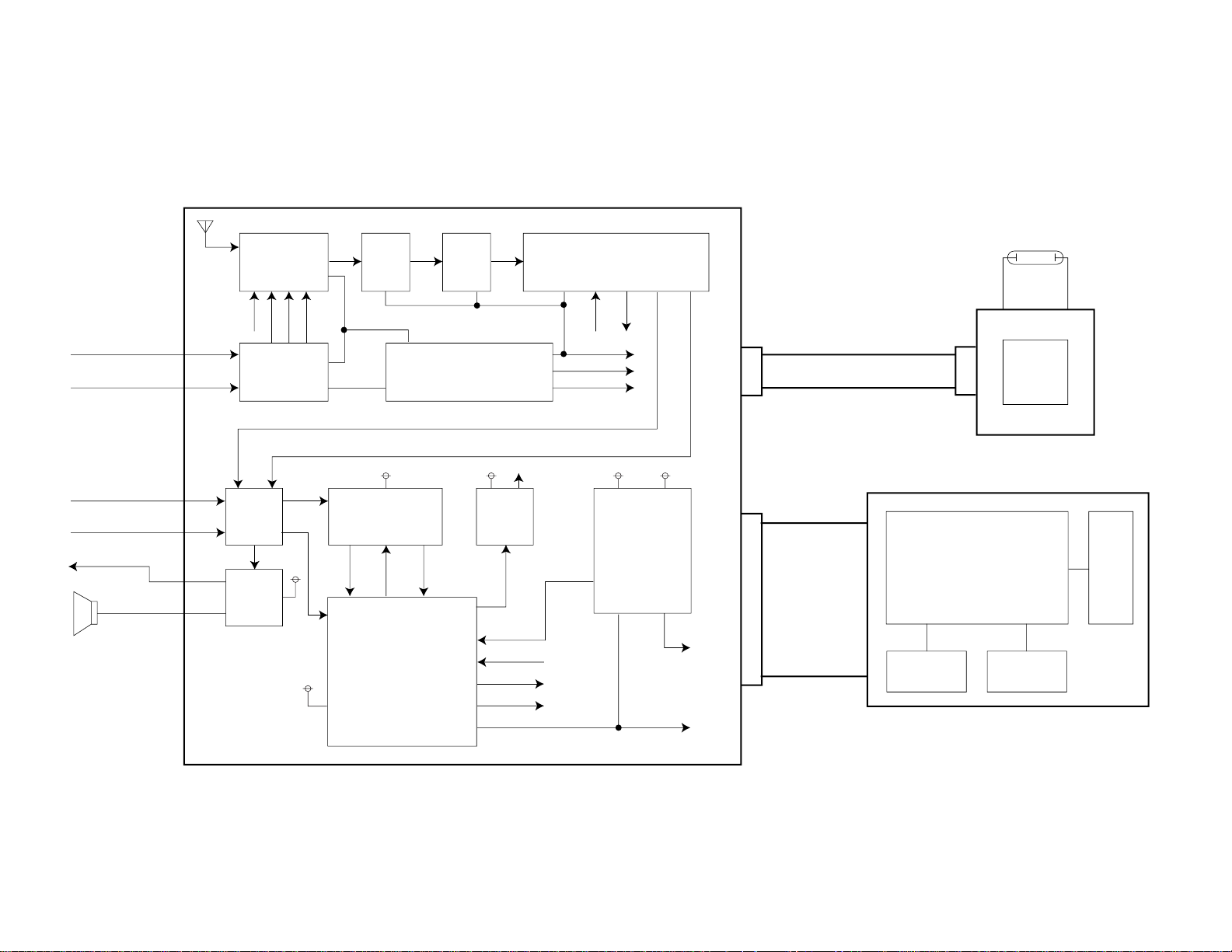
TUNER
(TEAA1)
PRE
AMP
ANT
SAW
FILTER
VIF/SIF
(M51348FP)
POWER SW
BAND SW
DC DC
CONVERTER
TRANS
BATTERY 1.5 V × 4
AC ADAPTOR 6V
EXTERNAL VIDEO
EXTERNAL AUDIO
EAR PHONE
SP
AUDIO2
VCC1-1
VCC2
VCC2 (4.0 V)
VCC7 (40 V)
VEE1 (—5 V)
AV
JACK
AUDIO AMP
NJM2070M
VCC2
TU
VCC2-8
AFI
UV
HL
A MUTF
MODULE
VIDEO2
AVB
VCC7 BT
VCC2 (4.7 V)
VCC1-1
VEE1VCC7
CHROMA
M52042FP
TUNING
BT GEN
BA 10358
VOLTAGE
SUPLLY
FOR LCD
DRIVER
A D CONVERTER
CONTROLLER
OM6006
INVERTER
IRANS
BL-PCB
LAMP
VCC1-1 GND
CN710
CN950
LCD DRIVER 5151
BTBVBS
U. V
AUDIO1
VIDEO1
A-MUTE
AFT
AUDIO1
VIDEO1
RGB
HD
C-SYNC
CN700
LCD
LCM
L-PCB
LCD DRIVER
051
LCD DRIVER
051
VCC2-0 GND
V1. V3. V0. V4. VO
CK1. CK2
D1~ 6
SNB STR
CNB2. CDB2. CFB2
EN1. EN2
MODULE
POWER
SUPPLY
BLOCK DIAGRAM
Page 5
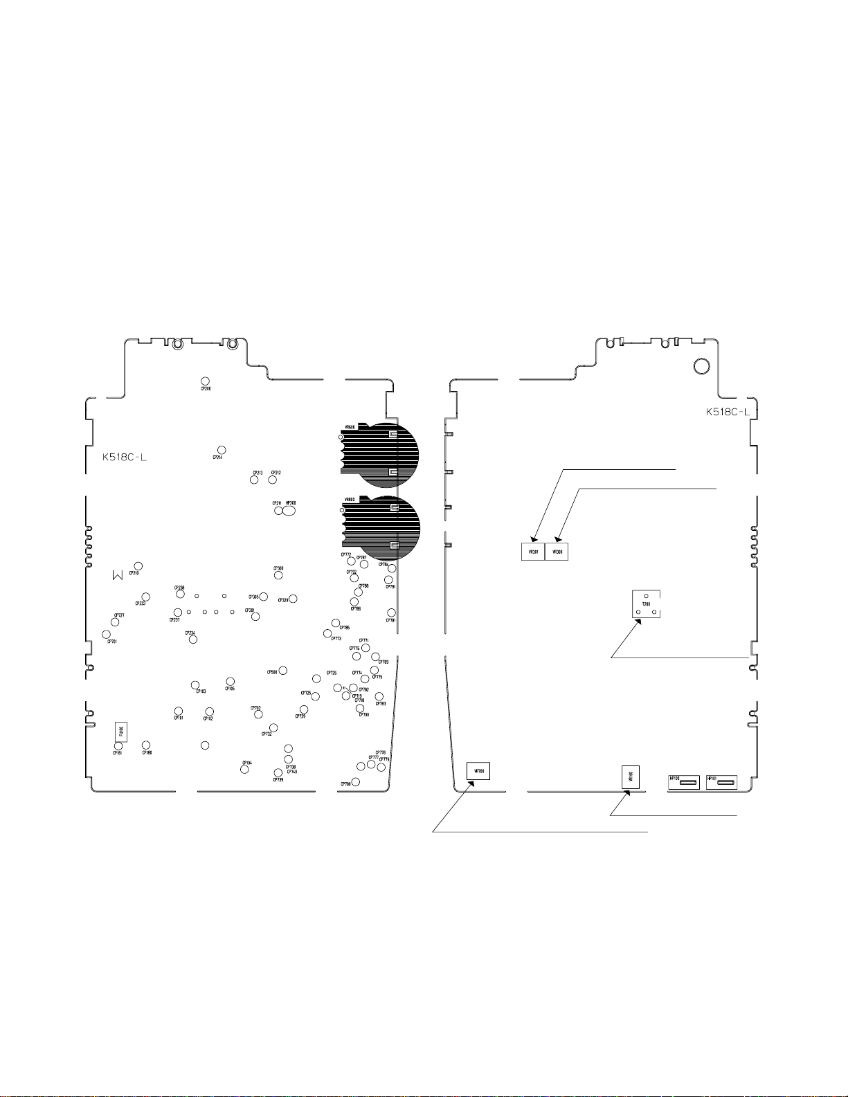
ADJUSTMENT
1. VCC2 adjustment, VCC7, VEE1 voltage check
2. LLD coil adjustment
3. Free running frequency adjustment
4. Contrast adjustment
5. TINT pot adjustment
Preparations
1. Connect AVB (CP725) to GND.
2. Set SW100 on UHF mode.
Adjustment And Test Point Locations
VR301 : Tint adjustment
VR300 : Contrast adjustment
Top View
T200 : LLD Coil adjustment
VR100 : VCC2 adjustment
VR700 : VCO free run frequency adjustment
Bottom View
— 3 —
Page 6
Adjustment procedures (TV-880C/I/N)
1. VCC2 adjustment, VCC7, VEE1 voltage check
• Condition
Power supply: Vcc1-1 = 5.0 ± 0.05 [V]
• Adjustment
Apply 5.0 ± 0.05 [V] on Vcc1-1 (CP101).
Adjust VR100 so that Vcc2 (CP102) voltage becomes 4.00 ± 0.02 [V].
• Checking
VCC7 (CP103) = 36.0 ~ 44.0 [V]
VEE1 (CP104) = –4.5 ~ –5.5 [V]
• Block diagram
VCC7
VCC1-1
L-PCBStabilizer
VCC2
VEE1
V
Digital
Voltmeter
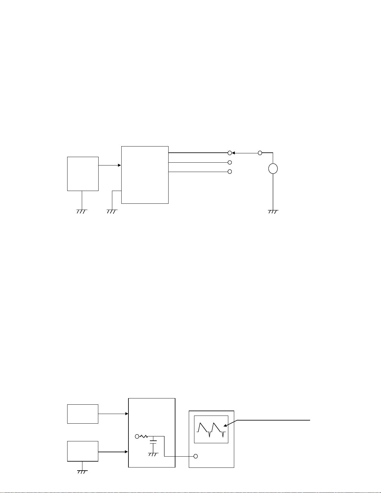
2. LLD coil adjustment
• Conditions
(1) Signals
Broadcasting system: B/G,H
Color system: PAL color bar
(2) Signal level
Input electric field: 40 ± 3dBµ (IF AGC full gain), P/S = 10 dB
(3) Other conditions
CCIR IF (Input electric field: terminated with 75-ohm resistance)
Power supply: Vcc1-1 = 5.0 ± 0.05 [V]
• Adjustment
Monitor video detection signal (CP238) via a low-pass filter of 100 kHz cutoff frequency and adjust
LLD coil T200 so that its DC level is minimum (waveform’s amplitude is maximum).
(Reference: C= 1500 pF, R = 1 Kohm)
• Confirmation
There should be no waveform distortion (erroneous synchronization, etc.), under sensitivity (video
detector output level is abnormally small, etc.).
• Block diagram
Signal
generator
IF signal
L-PCB
Adjust to minimize the DC level.
Stabilizer
VCC1-1
Detector OUT
Low-Pass Filter
DC IN
Oscilloscope
— 4 —
Page 7
3.Free running frequency adjustment
• Conditions
(1) Signal
No signal (PAL standard signal should be applied only at synchronous check)
(2) Signal level
Input electric field only at synchronous check: 70 dBµ (terminated with 75-ohm resistance),
P/S = 10 dB
(3) Other conditions
CCIR IF input only at synchronous check (input electric field with 75-ohm termination).
Connect SYF terminal (CP729) and VCC2-7.
Power supply: Vcc1-1 = 5.0 ± 0.05 [V]
Room temperature: 20 ± 10 [°C]
• Adjustment
Monitoring HDB (CP305) with a frequency counter, adjust VR700 so that the frequency is 15.625 ±
0.1 [kHz].
• Caution
(1) Disconnect the wire between SYF terminal and VCC2-7.
Applying IF signal make sure that synchronization is normal on the display.
(2) Use input signal pattern conforming CCIR standard.
• Block diagram
Signal
generator
VCC1-1
Stabilizer
4.Contrast adjustment
• Conditions
(1) Signal
Broadcasting system: B/G,H
Color system: PAL color bar
(2) Signal level
Input electric field: 70 dBµ (terminated with 75-ohm resistance), P/S = 10 dB
(3) Other conditions
CCIR IF input (input electric field should be terminated with 75-ohm resistance).
Apply voltage of Vcc1-1 = 5.0 ± 0.05 [V]
L-PCB
SYF
HD
VCC2-7
Frequency
Counter
• Adjustment
Connect color terminal (CP320) to GND (CP300) so that screen becomes black and white. Adjust
contrast pot VR300 so that the voltage between pedestal level and white level of B signal (CP740) is
0.80 ± 0.05 [Vp-p].
— 5 —
Page 8

• Caution
(1) Make sure that there is no distortion on the waveforms.
(2) Connect COLOR terminal of Chroma IC (M52045FP) to GND.
(3) Monitor the B output signal with an oscilloscope via a low-pass filter (C = 2700 pF, R = 100 ohm).
• Block diagram
Signal
generator
Stabilizer
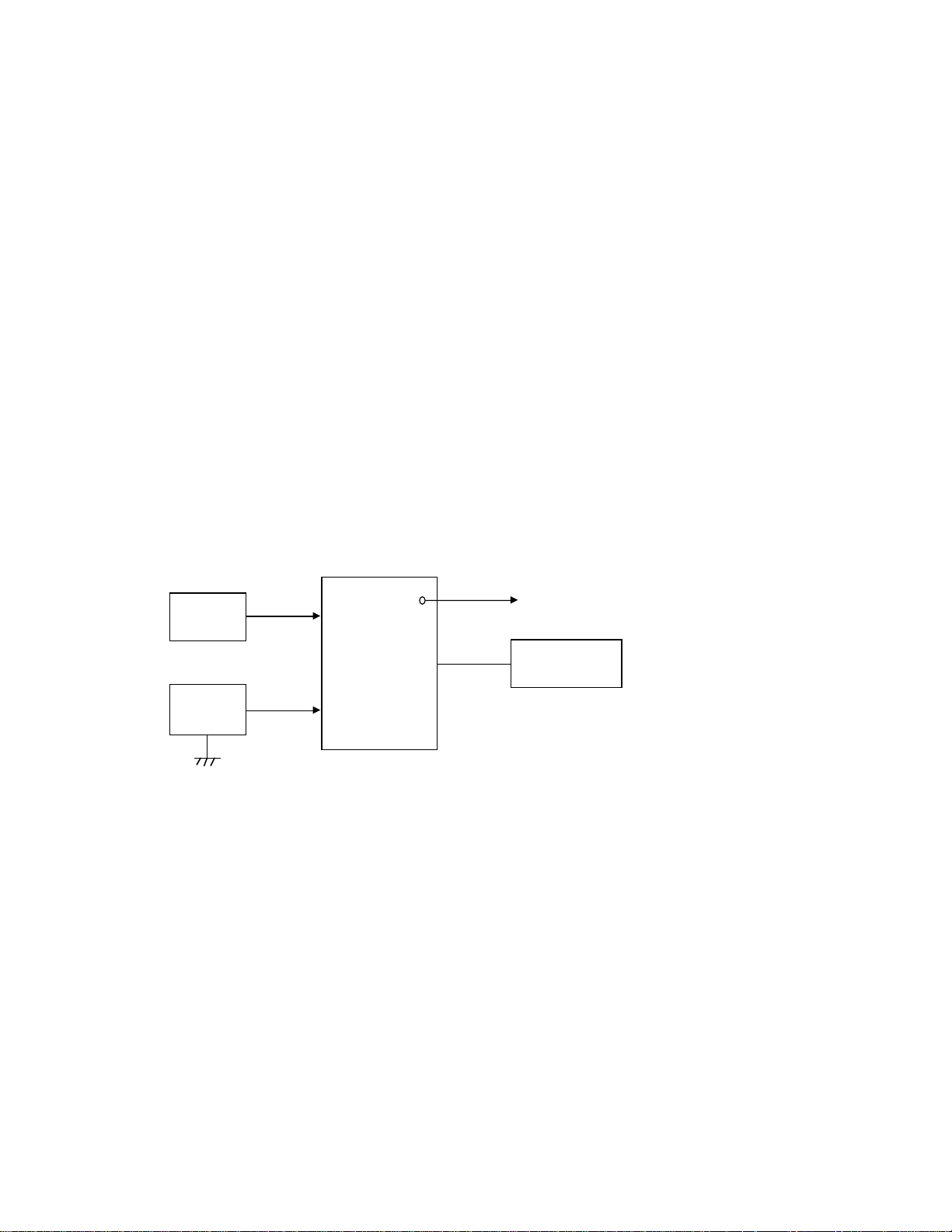
5.TINT pot adjustment
• Condition
(1) Signal
Broadcasting system: B/G,H
Color system: PAL color bar
(2) Signal level
Input electric field: 70 dBµ (75-ohm termination), P/S = 10 dB
(3) Other conditions
CCIR IF input (input electric field should be terminated with 75-ohm resistance).
Apply voltage of Vcc1-1 = 5.0 ± 0.05 [V]
• Adjustment
Observing output signal B with an oscilloscope, adjust TINT pot VR301 so that the wave from H and
H' will be same.
L-PCB
White level
B output
Pedestal level
VCC1-1
Oscilloscope
Low-Pass Filter
• Caution
Do not connect COLOR terminal to GND.
Monitor B output signal with an oscilloscope via a low-pass filter (C = 2700 pF, R = 100 ohm).
• Block diagram
Signal
generator
VCC1-1
Stabilizer
L-PCB
B output
Low-Pass Filter
Oscilloscope
HH’
— 6 —
Page 9

Adjustment procedures (TV-880D)
1. VCC2 adjustment, VCC7, VEE1 voltage check
• Condition
Power supply: Vcc1-1 = 5.0 ± 0.05 [V]
• Adjustment
Apply 5.0 ± 0.05 [V] on Vcc1-1 (CP101).
Adjust VR100 so that Vcc2 (CP102) voltage becomes 4.00 ± 0.02 [V].
• Checking
VCC7 (CP103) = 36.0 ~ 44.0 [V]
VEE1 (CP104) = –4.5 ~ –5.5 [V]
• Block diagram
VCC7
VCC1-1
L-PCBStabilizer
VCC2
VEE1
V
Digital
Voltmeter
2. LLD coil adjustment
• Conditions
(1) Signals
Broadcasting system: I
Color system: PAL color bar
(2) Signal level
Input electric field: 40 ± 3dBµ (IF AGC full gain), P/S = 7 dB
(3) Other conditions
UK IF (Input electric field: terminated with 75-ohm resistance)
Power supply: Vcc1-1 = 5.0 ± 0.05 [V]
• Adjustment
Monitor video detection signal (CP238) via a low-pass filter of 100 kHz cutoff frequency and adjust
LLD coil T200 so that its DC level is minimum (waveform’s amplitude is maximum).
(Reference: C= 1500 pF, R = 1 Kohm)
• Confirmation
There should be no waveform distortion (erroneous synchronization, etc.), under sensitivity (video
detector output level is abnormally small, etc.).
• Block diagram
Signal
generator
IF signal
L-PCB
Adjust to minimize the DC level.
Stabilizer
VCC1-1
Detector OUT
Low-Pass Filter
DC IN
Oscilloscope
— 7 —
Page 10

3.Free running frequency adjustment
• Conditions
(1) Signal
No signal (PAL standard signal should be applied only at synchronous check)
(2) Signal level
Input electric field only at synchronous check: 70 dBµ (terminated with 75-ohm resistance),
P/S = 7 dB
(3) Other conditions
UK IF input only at synchronous check (input electric field with 75-ohm termination).
Connect SYF terminal (CP729) and VCC2-7.
Power supply: Vcc1-1 = 5.0 ± 0.05 [V]
Room temperature: 20 ± 10 [°C]
• Adjustment
Monitoring HDB (CP305) with a frequency counter, adjust VR700 so that the frequency is 15.625 ±
0.1 [kHz].
• Caution
(1) Disconnect the wire between SYF terminal and VCC2-7.
Applying IF signal make sure that synchronization is normal on the display.
(2) Use input signal pattern conforming UK standard.
• Block diagram
Signal
generator
VCC1-1
Stabilizer
4.Contrast adjustment
• Conditions
(1) Signal
Broadcasting system: I
Color system: PAL color bar
(2) Signal level
Input electric field: 70 dBµ (terminated with 75-ohm resistance), P/S = 7 dB
(3) Other conditions
UK IF input (input electric field should be terminated with 75-ohm resistance).
Apply voltage of Vcc1-1 = 5.0 ± 0.05 [V]
L-PCB
SYF
HD
VCC2-7
Frequency
Counter
• Adjustment
Connect color terminal (CP320) to GND (CP300) so that screen becomes black and white. Adjust
contrast pot VR300 so that the voltage between pedestal level and white level of B signal (CP740) is
0.80 ± 0.05 [Vp-p].
— 8 —
Page 11

• Caution
(1) Make sure that there is no distortion on the waveforms.
(2) Connect COLOR terminal of Chroma IC (M52045FP) to GND.
(3) Monitor the B output signal with an oscilloscope via a low-pass filter (C = 2700 pF, R = 100 ohm).
• Block diagram
Signal
generator
Stabilizer
5.TINT pot adjustment
• Condition
(1) Signal
Broadcasting system: I
Color system: PAL color bar
(2) Signal level
Input electric field: 70 dBµ (75-ohm termination), P/S = 7 dB
(3) Other conditions
UK IF input (input electric field should be terminated with 75-ohm resistance).
Apply voltage of Vcc1-1 = 5.0 ± 0.05 [V]
• Adjustment
Observing output signal B with an oscilloscope, adjust TINT pot VR301 so that the wave from H and
H' will be same.
L-PCB
White level
B output
Pedestal level
VCC1-1
Oscilloscope
Low-Pass Filter
• Caution
Do not connect COLOR terminal to GND.
Monitor B output signal with an oscilloscope via a low-pass filter (C = 2700 pF, R = 100 ohm).
• Block diagram
Signal
generator
VCC1-1
Stabilizer
L-PCB
B output
Low-Pass Filter
Oscilloscope
HH’
— 9 —
Page 12

TOP VIEWS
Linear
PRINTED CIRCUIT BOARDS
Back Light
— 10 —
Page 13

BOTTOM VIEWS
Linear
Back Light
— 11 —
Page 14

EXPLODED VIEW
25
24
22
20
23
13
11
17
15
14
10
7
8
12
26
13
18
6
9
21
29
2
16
19
3
27
1
5
— 12 —
428
Page 15

PARTS PRICE LIST
TV-880C/I/N/D
N
Item
Code No.
Parts Name
Specification
Price Code
RCIND
LINEAR PCB
Connector
N
CN700
35021718
Connector
52559-2290
111
1
AE
X
N
CN710
35022586
Connector
9210B-1-04Z604-T
111
1
AC
X
Diodes
D100
71011194
Chip diode
MA111-(TX)
111
1
AA
CND110
23603092
Chip zener diode
MA8047-L(TX)
111
1
AACD150
71011194
Chip diode
MA111-(TX)
111
1
AACD152
23901379
Schottky diode
MA729-(TX)
111
1
ABCD155
23901470
Chip diode
MA143A-(TX)
111
1
AACD180
23901190
Diode
ERA15-01Y
111
1
AACD280
71011194
Chip diode
MA111-(TX)
111
0
AA
CND500
23603079
Chip zener diode
MA8300-M(TX)
111
1
AACD701
71011194
Chip diode
MA111-(TX)
111
1
AACD801
23901477
Chip diode
MA142WA-(TX)
111
1
AACD802
23901470
Chip diode
MA143A-(TX)
111
1
AACD803
23901470
Chip diode
MA143A-(TX)
111
1
AA
C
Filter
N
F200
30251834
SAW filter
SAF38.9MZ210Z
111
0
AJ
C
N
F200
30251855
SAW filter
SAF39.5MZ210Z
000
1
AJ
C
N
F210
30251952
SIF filter
SFSH5.5MCB
111
0
AB
C
N
F210
30251955
SIF filter
SFSH6.0MCB
000
1
AB
C
N
F220
38512108
Ceramic discriminator
CDSH5.5MC30K
111
0
AB
C
N
F220
38512111
Ceramic discriminator
CDSH6.0MC30K
000
1
AE
C
F230
38501372
SIF trap
TPS5.5MB
111
0
AC
C
F230
38510553
SIF trap
TPS6.0MB
000
1
AC
C
Fuse
FU100
27975509
Chip fuse
PI-R429001
111
1
AD
A
Oscillator
H300
25902717
Crystal oscillator
HD-49-4.43M
111
1
AE
C
Ics
IC200
21141827
Linear IC
M51348FP-T1
111
1
AR
B
IC300
21143311
Linear IC
M52045FP-T1
111
1
AW
B
IC500
21160119
OP amplifier
BA10358F-T1
111
1
AC
B
IC600
21142464
Linear IC
NJM2070M-T1
111
1
AF
B
IC700
20126038
LSI
ML9661GA-6006
111
1
BB
B
N
IC710
21145866
IC
S-81230SGUP-DQB-T1
111
1
AC
B
Jacks
JK100
35018281
Power jack
HEC0811-010010
111
1
AD
C
JK250
35013773
Headphone jack
HSJ6063-01-410
111
1
AH
C
JK600
35015439
Jack
HSJ1456-01-210
111
1
AC
C
Inductors
N
L101
30132583
Chip inductor
NLCD322522-470K-TP
111
1
AA
X
N
L200
30132585
Chip inductor
NLCD322522-101K-TP
111
1
AA
X
L201
30132585
Chip inductor
NLCD322522-101K-TP
111
1
AA
X
N
L210
30132650
Chip inductor
LK1608-2R7K-TP
111
1
AB
X
N
L220
30132268
Chip inductor
LK1608-150K-TP
111
1
AA
X
L300
30132585
Chip inductor
NLCD322522-101K-TP
111
1
AA
X
L700
30450028
Chip inductor
BK1608HS601-T
111
1
AA
X
L800
30450028
Chip inductor
BK1608HS601-T
111
1
AA
X
Transistors
Q101
22530133
Chip transistor
2SD1819A-R(TX)
111
1
AACQ110
22530133
Chip transistor
2SD1819A-R(TX)
111
1
AACQ111
22530308
Chip transistor
2SD1119-R(TX)
111
1
AC
CNQ200
22501617
Chip transistor
2SC4417-(TX)
111
1
ABCQ280
22591491
Digital transistor
UN5213-(TX)
111
0
AACQ300
22530133
Chip transistor
2SD1819A-R(TX)
111
1
AACQ800
22530133
Chip transistor
2SD1819A-R(TX)
111
1
AACQ801
22530133
Chip transistor
2SD1819A-R(TX)
111
1
AACQ803
22510189
Chip transistor
2SB1218A-R(TX)
111
1
AACQ804
22510189
Chip transistor
2SB1218A-R(TX)
111
1
AA
CNQ810
22530716
Chip transistor
2SD1824-S(TX)
111
1
AA
C
Quantity
NOTE: Q - Quantity per unit
- 13 -
R - Rank
Page 16

N
Item
Code No.
Parts Name
Specification
Price Code
RCIND
Quantity
Q811
22530133
Chip transistor
2SD1819A-R(TX)
111
1
AACQ813
22510189
Chip transistor
2SB1218A-R(TX)
111
1
AACQ820
22530133
Chip transistor
2SD1819A-R(TX)
111
1
AACQ821
22530133
Chip transistor
2SD1819A-R(TX)
111
1
AACQ822
22530133
Chip transistor
2SD1819A-R(TX)
111
1
AA
C
Switch
SW100
34120938
Slide switch
ESD-11V231
111
0
AD
C
SW100
34121134
Slide switch
ESD-11V221
000
1
AD
C
Converter
N
T100
30650730
DC/DC converter
LC12U-45
111
1
AE
B
Coils
T200
38410700
Coil
5KAC-03A
111
1
AE
X
T201
38410700
Coil
5KAC-03A
111
1
AE
X
Thermistor
N
TM100
27753448
Chip thermistor
NTH5G1M31B102K04TH
111
1
AB
C
Tuners
TU200
10135315
Tuner
TEPE5-01
111
0
BT
B
TU200
10148570
Tuner
TEPB5-05
000
1
BR
B
Variable resistors
N
VR100
27752800
Chip semi-fixed resistor
EVN5ESX50B24
111
1
AA
C
VR200
27752765
Chip semi-fixed resistor
EVN5ESX50B54
111
1
AA
C
VR300
27752758
Chip semi-fixed resistor
EVN5ESX50B14
111
1
AA
C
VR301
27752765
Chip semi-fixed resistor
EVN5ESX50B54
111
1
AA
C
VR600
27650616
Volume
RK09H11T-10KB
111
1
AD
C
VR700
27752786
Chip semi-fixed resistor
EVN5ESX50B53
111
1
AA
C
VR800
27650623
Volume
RK09H11T-20KB
111
1
AD
C
BL PCB
Connector
CN950
35021550
Connector
9110S-04
111
1
AA
X
Coil
L900
30130756
Choke coil
RCH-875-101K
111
1
AD
X
Transistors
Q900
22530308
Chip transistor
2SD1119-R(TX)
111
1
ACCQ901
22530308
Chip transistor
2SD1119-R(TX)
111
1
AC
C
Switchs
SW700
34121029
Switch
SKHHAL
111
1
AA
C
SW701
34121029
Switch
SKHHAL
111
1
AA
C
Transformer
T900
30121588
Inverter trans
C-8123
111
1
AL
B
MAIN COMPONENT
N166137030
Lower case BIM-K518
K140511-1
101
1
AF
X
N166138380
Lower case IAM-K518
K140511-3
010
0
AF
X
N266137060
Battery cover A-K518
K241047-1
111
1
AA
C
3
38511267
Rod antenna
YH810721
111
1
AQ
B
N466137180
Stand B-K518
K241040-1
111
1
AA
C
N566138350
Rating plate CIM-K518
K341435-3
100
0
AA
X
5
66138360
Rating plate NAM-K518
K341435-5
001
0
AA
X
N566138920
Rating plate DAM-K518
K341435-6
000
1
AA
X
N566138370
Rating plate IAM-K518
K341435-7
010
0
AA
X
N666137170
Jack plate B-K518
K241058-1
111
1
AA
X
N766138340
Upper case ass'y
K341446*3
100
0
AU
X
N766138341
Upper case ass'y
K341446*4
001
0
AU
X
N766138342
Upper case ass'y
K341446*5
010
0
AU
X
N766138914
Upper case ass'y
K341446*6
000
1
AU
X
N866138301
Upper case CIM-K518
K140510A-4
100
0
AG
X
N866138391
Upper case NAM-K518
K140510A-6
001
0
AG
X
N866138311
Upper case IAM-K518
K140510A-5
010
0
AK
X
N866138291
Upper case DAM-K518
K140510A-3
000
1
AG
X
NOTE: Q - Quantity per unit
- 14 -
R - Rank
Page 17

N
Item
Code No.
Parts Name
Specification
Price Code
RCIND
Quantity
N966137040
Switch knob A-K518
K341342-1
111
1
AA
X
N1066140900
Adhesive tape C-K518
K441586-3
111
1
AA
X
N1166137260
Adhesive tape B-K518
K441586-2
111
1
AA
X
12
60207658
Battery spring B-1-G513
P408A-1
111
1
AB
X
13
60207666
Battery springB-2-G513
P409A-1
222
2
AA
X
N1466137270
Tuning button A-K518
K241046-1
111
1
AA
X
N1566137280
Display plate BIM-K518
K241045-1
101
1
AK
C
N1566138401
Display plate IAM-K518
K241045A-2
010
0
AK
C
N1666138320
Linear PCB ass'y
K241113*1
111
0
DM
B
N1666138915
Linear PCB ass'y
K241129*1
000
1
DM
B
N1766137210
Battery spring A-K518
K441546-1
111
1
AA
X
N1866137220
Battery spring B-K518
K441547-1
111
1
AA
X
N1966137230
antenna terminal A-K518
K341343-1
111
1
AA
X
N2066137290
Reflector case A-K518
K140528-1
111
1
AJ
X
N2166137018
BL unit
K341437*1
111
1
EH
B
22
38512093
Fluorescent lamp
3064BB-CA48
111
1
AV
A
23
66129730
Light diffuser sheet A-K516
K340975-1
111
1
AC
X
N2427251363
LCD
CMG23C1-TO
111
1
CZ
C
N2566137300
sealed case A-K518
K241038-1
111
1
AB
X
N2638311095
Speaker
28-8AB-09
111
1
AS
C
27
66091290
Screw A-K610
K412031-1
111
1
AA
C
28
66099630
Screw A-K720
K410188-6
111
1
AA
C
29
58600532
Screw
BT31.7X9
111
1
AA
C
C
:TV-880C(PAL B/G,H)
I
:TV-880I(PAL B/G)
N
:TV-880N(PAL B/G,H)
D
:TV-880D(PAL I)
NOTE: Q - Quantity per unit
- 15 -
R - Rank
Page 18

LINEAR (TV-880C/I/N)
Antenna
SCHEMATIC DIAGRAMS
Audio Amplifier CircuitIF Detection Circuit
External
Tunner
Antenna
Jack
Earphone
Jack
Speaker
Chroma Circuit
Tunner
Power Switch
Power Supply Circuit
Tuning Voltage Generator Circuit
40 V
4.0 V
–5 V
— 16 —
Display Controller Circuit
Display Generator Voltage Circuit
Page 19

LINEAR (TV-880D)
External
Tunner
Antenna
Antenna
Jack
Audio Amplifier CircuitIF Detection Circuit
Earphone
Jack
Speaker
Chroma Circuit
Tunner
Power Switch
Power Supply Circuit
Tuning Voltage Generator Circuit
40 V
4.0 V
–5 V
— 17 —
Display Controller Circuit
Display Generator Voltage Circuit
Page 20

BACK LIGHT
Notes:
1. All resistance values are indicated in "ohms" (k=103 ohms, M=106 ohms).
2. All capacitance values are indicated in "µF" (p=10-6 µF).
3. All inductance values are indicated in "µH."
— 18 —
Page 21

CASIO TECHNO CO.,LTD.
Overseas Service Division
Nishi-Shinjuku Kimuraya Bldg. 1F
5-25, Nishi-Shinjuku 7-Chome
Shinjuku-ku, Tokyo 160-0023, Japan
 Loading...