

Page 1
R
(without price)
TV-1800C(PAL B / G,H)
TV-1800D(PAL I)
TV-1800I (PAL B / G)
TV-1800N(PAL B / G,H)
(KX-523)
DEC. 1996
<
TUNING
>
Page 2

CONTENTS
Page
SPECIFICATIONS.....................................................................................1
BLOCK DIAGRAM.................................................................................... 2
CIRCUIT OPERATIONS ...........................................................................3
PRINTED CIRCUIT BOARDS...................................................................4
PARTS LIST.............................................................................................. 6
EXPLODED VIEW.....................................................................................9
SCHEMATIC DIAGRAMS.......................................................................11
WAVEFORMS ......................................................................................... 14
Page 3
SPECIFICATIONS
Item Specification
1. Power voltage DC 6.0 V
2. Power consumption Approx. 3.6 W
3. Current consumption Approx. 600 mA
4. Battery life (with alkaline batteries) Approx. 2.5 hours
Batteries : 4 × LR6 (D) size batteries
5. Power supply Car adaptor : CA-K65
AC adaptor : AD-K65
Earphone jack : 3.5 ø mini
6. Connection terminals External power jack : 6.0 V DC IN
External antenna jack : 3.5 ø mini
7. Screen size 2.5 inches
8. No. of picture element 115,020 (540 × 213) dots
9. Dimensions 135 mm (H) × 91 mm (W) × 38 mm (D)
10. Weight 240 g without batteries
AC adaptor : AD-K65
11. Options Car adaptor : CA-K65
Antenna matching device : AS-35S
Model Color System TV System Channel
TV-1800C/N PAL B/G, H CCIR VHF: 2 ~ 12 ch UHF: 21 ~ 69 ch
TV-1800D PAL –/I UK — UHF: 21 ~ 68 ch
TV-1800I PAL B/G ITALY VHF: A ~ H2 ch UHF: 21 ~ 69 ch
— 1 —
Page 4
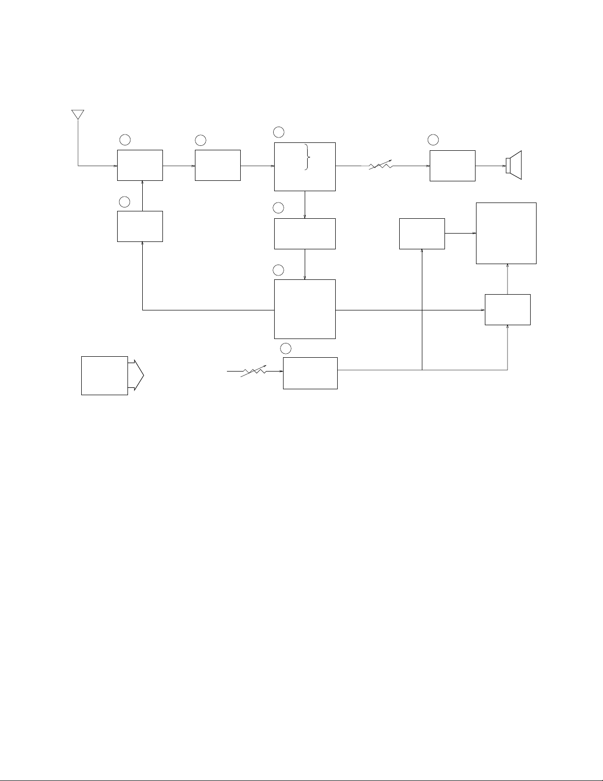
Antenna
BLOCK DIAGRAM
Power
Supply
1 TU200 2 Q200
IF Amp.Tuner
7
IC500
Tuning
Voltage
Generator
VCC2 (3.95V)
VCC7 (41.6~51.6V)
VEE1 (-6.5~-8.0V)
VR800
Brightness
Control
3 IC200
Video
Sound Det.
FM
AFT Circuit
AGC Circuit
5
6
Osc.
Display
Control
A-D Converter
Auto-Tuning
Control
8 Q800~Q806
Det
IC300
Chroma
Circuit
IC700
Display
Voltage
Generator
VR600
Volume
Control
4 IC600 Speaker
Audio
Amp.
Common
Driver
LCD
Segment
Driver
1 — Color Tuner: TU200 TEPE5-01(TV-1800C/I/N) TU200 TEPB5-05(TV-1800D)
Selects a desired radio wave and changes it to the video IF signal.
2 — Video IF Amp.: Q200 2SC4238
Amplifies the video IF signal output from the tuner TU by 10 times (20 dB).
3 — Video Det./Sound Det./FM Det./AFT/AGC: IC200 M51348FP
Eliminates the carrier wave in the video IF signal, and picks up the video signal and the sound IF signal.
Also, the sound signal is picked up from the sound IF signal by FM detection.
4 — Audio Amp.: IC600 NJM2070M
Sound amplification.
5 — Chroma Circuit: IC300 M52045FP
Generates the tricolor (red, green, and blue) from the video signal.
6 — OSC/A-D Converter/Display Control/ Auto-Tuning Control : IC700 MSM662501 GSK-640E
Converts the color signal into a digital signal.
Also, generates the clock pulse for the display and controls the display.
7 — Tuning Voltage Generator: IC500 MSC1169MS-K
Generates the tuning voltage with the tuning pulse (TU) output from 6.
8 — Display Voltage Generator: IC800 BA10358F, Q800 ~ Q806 Q810 Q811 2SD1149S,
2SD601A-R×3, 2SB709A-R
Generates the display voltages V0 ~ V4 with VEE1 and VCC7 outputs from the power supply.
— 2 —
Page 5
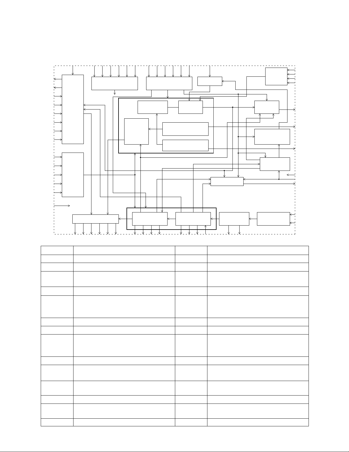
CIRCUIT OPERATIONS
AD2
AD1
RLL
VDD2
RHH
M7
M8
M9
M10
PSi
VSS1
IC700
B
G
R
VSS2 TE1
A/D
Mode
Control
Data Output
TE2
TE4
TE5
TE6
M6 M5 M4 M3 M2 M1 AFT
Frequency
Divider
Channel
bar
Control
Vertical
positioning
Control
TE3
Test Control Mode Control
Test
Circuit
Display
Control
Sweep
Control
Tuning Control
Tuning Voltage
UP/DOWN Counter
Pulse Width
Modulation D/A
Horizontal
positioning
Control
AFT
Control
Phase
Comparator
Frequency
Divider
Key
Switch
Control
Mute
Control
Synchronism
Judgment
Frequency
Separator
Oscillator
KDB
KCB
AVB
UHF
MTB
VLB
TU
VDD1
C-S
PD
OSC1
OSC2
D1 D2 D3 D4 D5 D6 CDB CFB CNB ECB
Signal Name
Function
SCB STB HDB CK1 CK2
SNB
Signal Name
Function
D1 ~ D6 Display data output terminal MTB Mute control terminal
SNB Data latch signal TU Tuning control pulse output terminal
CDB Scanning start signal VLB VHF High/Low channel select signal
output terminal
CFB Output voltage changeover signal UHF VHF/UHF select signal
CNB Scanning signal shift lock signal AVB
KCB Key input terminal
KDB
SCB Brightness modulation pulse control AFT AFT voltage input terminal
STB Sampling start signal M1 ~ M10 Mode select signal input terminal
ECB Signal input terminal controlling the
TE1 ~ TE6
Test terminal
segment drive terminal to "H" during
no display
CK1, CK2 Clock pulse output terminal R, G, B Original color
OSC1 Oscillator frequency control terminal RLL "L" level voltage input terminal of
OSC2 video signal
PD Clock pulse adjustment terminal RHH "H" level voltage input terminal of
video signal
C-S Synchronizing pulse input terminal PS1 Mode control signal
HDB Horizontal synchronizing signal input VSS1 Power supply voltage input terminal
terminal
VDD1 VDD voltage input terminal
— 3 —
Page 6

TOP VIEWS
Linear
PRINTED CIRCUIT BOARDS
C105
SW100
JK100
C100
FU100
D180
JK200
TU200
L102
T100
C115
C309
CN701
C110
L101
C112
H300
C202
C113
R133
R313
R342
R210
R209
R247
R314
C233
R207
F203
C305
T201 T200
L202
R700
D703
R704
R718
R705
C760
C306
C236
C205
C207
R734
F200
R222
R239
C700
R725
R738
C208
D803
R727
D705
C845
R726
C741
R703
R719
C603
F201
R824
C810
C761
R733
C808
R808
C751
L705
C756
JK600
C210
F202
R825
C606
C806
C750
C755
C600
CN700
VR600
VR800
C836
C831
C832
Back Light
L950
C925
R950
C950C951
— 4 —
T950
C927
Page 7

BOTTOM VIEWS
Linear
R836
R835
R834
R820
R821 C840
R822
Q810
Q811
IC600
R606
IC800
R607
R229
C830
Q806
R833
R817
C835
R816
R641
R611
R615
Q804
R815
C765
D805
R645
C630
R610
CP245
C257
Q801
CP700
R730
C642
C249
Q805
R819
Q803
IC700
R208
R830
VR700
C239
C240
R230
R827
Q802
R810
Q800
C243
C246
IC200
R809
R312
C776
L200
C261
D700
L700
C740
C742
C345
C339
R740
R202
VR200
C263
C291
CP703
R311
R204
R215
C264
C262
VR300
R322
C346
Q200
HP200
C245
R212
R241
R246
C290
C340
R325
VR301
C237
CP221
C259
R236
R223
D500
CP240
C335
R310
IC300
R343
R205
R203
R201
R224
D150
Q300
C347
C235
R502
R541
R550
R545
C351
R115
D152
R306
R307
R336
R503
R501
IC500
C545
R111
+
C301
R335
R331
R330
C350
C234
C140
C146
R305
R326
C265
R500
R102
D155
D100
C550
C145
Q111
C185
CP204
VR100
C135
R103
R117
R101
Q100
Q101
R150
Back Light
FU900
SW701
FU901
SW700
— 5 —
Page 8

PARTS LIST
LINEAR PCB
Item Code No. Parts Name Specification Applicable Q R
Diodes
D100 2390 1176 Chip diode MA152WK-(TX) TV-1800 Common
D150 2390 1176 Chip diode MA152WK-(TX) TV-1800 Common
D152 2390 1176 Chip diode MA152WK-(TX) TV-1800 Common
D155 2390 1302 Chip diode MA153A-(TX) TV-1800 Common
D180 2390 2450 Chip diode SC016-2-TE12RA TV-1800 Common
D500 2360 1344 Chip zener diode MA3330-M(TX) TV-1800 Common
D700 2390 0469 Chip diode MA157A-(TX) TV-1800 Common
D703 2390 0469 Chip diode MA157A-(TX) TV-1800 Common
D705 2390 1358 Variable diode MA329-(TX) TV-1800 Common
D803 2390 0469 Chip diode MA157A-(TX) TV-1800 Common
D805 2390 1253 Chip diode MA152WA-(TX) TV-1800 Common
Fuse
FU100 3632 0245 Fuse ATSCR0.80A TV-1800 Common
ICs
IC200 2114 1827 Linear IC M51348FP-T1 TV-1800 Common
IC300 2114 3311 Linear IC M52045FP-T1 TV-1800 Common
IC500 2114 2842 Linear IC MSC1169MS-KR1-620 TV-1800 Common
IC600 2114 2464 Linear IC NJM2070M-T1 TV-1800 Common
IC700 2011 2695 LSI MSM6625-01GSK-640E TV-1800 Common
IC800 2116 0119 OP AMP BA10358F-T1 TV-1800 Common
Jacks
JK100 3501 6846 Jack HEC2500-010110 TV-1800 Common
JK200 3501 5439 Jack HSJ1456-01-210 TV-1800 Common
JK600 3501 5439 Jack HSJ1456-01-210 TV-1800 Common
Transistors
Q100 2210 8026 Chip transistor 2SB709A-R(TX) TV-1800 Common
Q101 2230 7011 Chip transistor 2SD601A-R(TX) TV-1800 Common
Q111 2253 0308 Chip transistor 2SD1119-R(TX) TV-1800 Common
Q200 2252 0707 Chip transistor 2SC4238-(TX) TV-1800 Common
Q300 2210 8026 Chip transistor 2SB709A-R(TX) TV-1800 Common
Q800 2230 7011 Chip transistor 2SD601A-R(TX) TV-1800 Common
Q801 2210 8026 Chip transistor 2SB709A-R(TX) TV-1800 Common
Q802 2230 7011 Chip transistor 2SD601A-R(TX) TV-1800 Common
Q803 2230 7011 Chip transistor 2SD601A-R(TX) TV-1800 Common
Q804 2230 7011 Chip transistor 2SD601A-R(TX) TV-1800 Common
Q805 2253 0476 Chip transistor 2SD1149-S(TX) TV-1800 Common
Q806 2230 7011 Chip transistor 2SD601A-R(TX) TV-1800 Common
Q810 2210 8026 Chip transistor 2SB709A-R(TX) TV-1800 Common
Q811 2230 7011 Chip transistor 2SD601A-R(TX) TV-1800 Common
Switches
SW100 3412 0938 Slide switch ESD-11V231 TV-1800C/I/N
SW100 3412 1134 Slide switch ESD-11V221 TV-1800D
Converter
T100 3065 0469 DC-DC converter LC12U-31 TV-1800 Common
Tuners
TU200 1013 5315 Tuner TEPE5-01 TV-1800C/I/N
TU200 1014 8570 Tuner TEPB5-05 TV-1800D
Variable resistors
VR600 2765 0616 Volume RK09H11T-10KB TV-1800 Common
VR800 2765 1582 Volume RK09H11T-100KB TV-1800 Common
C
1
C
1
C
1
C
1
C
1
C
1
C
1
C
1
C
1
C
1
C
1
B
1
C
1
C
1
C
1
C
1
C
1
C
1
C
1
C
1
C
1
B
1
B
1
B
1
C
1
C
1
C
1
C
1
C
1
C
1
C
1
C
1
C
1
C
1
C
1
C
1
C
1
B
1
C
1
C
1
C
1
C
1
Notes: Q – Quantity per unit
R – Rank
— 6 —
Page 9

BL PCB
Item Code No. Parts Name Specification Applicable Q R
Lamp
LA900 3851 1484 Fluorescent lamp 8.76AD1P2-CA11 TV-1800 Common
Fuses
FU900 3632 0308 Temperature fuse EYP-1BF102L TV-1800 Common
FU901 3632 0308 Temperature fuse EYP-1BF102L TV-1800 Common
Transistors
Q950 2253 0287 Chip transistor 2SD965-R TV-1800 Common
Q951 2253 0287 Chip transistor 2SD965-R TV-1800 Common
Switches
SW700 3412 1029 Switch SKHHAL TV-1800 Common
SW701 3412 1029 Switch SKHHAL TV-1800 Common
Transformer
T950 3012 1001 Inverter trans NT-04 TV-1800 Common
A
1
C
1
C
1
B
1
B
1
C
1
C
1
B
1
Notes: Q – Quantity per unit
R – Rank
— 7 —
Page 10

MAIN COMPONENT
Item Code No. Parts Name Specification Applicable Q R
1 6611 6560 Display plate CIM-K523 K440953-2 TV-1800C
1 6611 6670 Display plate DAM-K523 K440953-3 TV-1800D
1 6611 6580 Display plate NAM-K523 K440953-4 TV-1800I/N
2 6600 2220 Adhesive tape A-K52 K451-5 TV-1800 Common
3 6608 7271 Adhesive tape B-K502 K410903A-2 TV-1800 Common
4 6609 9680 Jack cover A-K611 K340237-1 TV-1800D/I/N
5 6608 6560 Switch knob A-K526 K311299-1 TV-1800 Common
6 6611 6521 Upper case CIM-K523 K110681A-8 TV-1800C/N
6 6611 6531 Upper case DAM-K523 K110681A-9 TV-1800D
6 6611 6541 Upper case IAM-K523 K110681A-10 TV-1800I
7 3831 0854 Speaker 28-8F-03 TV-1800 Common
8 6608 6330 Tuning button A-K526 K311318-1 TV-1800 Common
9 6608 6340 Ribbon K526 K411841-1 TV-1800 Common
10 6608 6301 Battery spring C-K526 K311313A-1 TV-1800 Common
11 6608 6311 Battery spring D-K526 K311314A-1 TV-1800 Common
12 6611 6610 Side case A-K523 K110691-2 TV-1800 Common
13 6610 9432 BL ass'y K211111B*1 TV-1800 Common
13-1 3851 1484 Fluorescent lamp 8.76AD1P2-CA11 TV-1800 Common
13-2 3632 0308 Temperature fuse EYP-1BF102L TV-1800 Common
13-3 6608 0170 Flat cable A-K541 K411565-1 TV-1800 Common
14 6608 6360 Battery spring A-K526 K311321-1 TV-1800 Common
15 6608 6370 Battery spring B-K526 K411830-1 TV-1800 Common
16 6611 6483 Linear PCB ass'y K340720*2 TV-1800C/I/N
16 6611 6484 Linear PCB ass'y K340720*3 TV-1800D
17 3851 1463 Rod antenna VR60114FA TV-1800 Common
18 6611 6600 Lower case BIM-K523 K110682-4 TV-1800C/D/N
18 6611 6640 Lower case IAM-K523 K110682-5 TV-1800I
19 6611 6620 Battery cover A-K523 K211023-2 TV-1800 Common
20 6611 2300 Stand A-K503 K310518-7 TV-1800 Common
21 6611 6670 Rating plate DAM-K523 K440954-4 TV-1800D
22 6611 6491 Display unit K340722*1 TV-1800 Common
23 5860 2380 Screw PS3 1.7X3.5 Bk TV-1800 Common
24 5860 0420 Screw BT3 1.7X4 Ni TV-1800 Common
25 5860 1449 Screw BT3 1.7X8 Bk TV-1800 Common
26 6605 0011 Screw A-K334 K410096A-1 TV-1800 Common
C
1
C
1
C
1
X
2
X
2
X
1
X
1
X
1
X
1
X
1
C
1
X
1
X
1
X
2
X
1
X
1
B
1
A
1
C
2
C
1
X
1
X
1
B
1
B
1
C
1
X
1
X
1
X
1
C
1
X
1
C
1
C
2
C
7
C
5
C
1
Notes: Q – Quantity per unit
R – Rank
— 8 —
Page 11

EXPLODED VIEW
23
25
11
24
12
5
13
13-3
10
3
2
8
3
24
9
13-1
13-2
1
2
4
6
7
22
15
17
19
16
14
24
20
25
24
24
18
25
26
21
— 9 —
Page 12

LINEAR (TV-1800C/I/N)
SCHEMATIC DIAGRAMS
Antenna
External Antenna
Jack
Tuner
IF pad
Batteries
1
DC in
3
2
IF detection Circuit
Earphone
Jack
Speaker
Audio Amplifier Circuit
13
Tuning Voltage Generator Circuit
10
9
Power Switch
4
8
Display Voltage Generator Circuit
To Back Light
6
7
5
11
12
14
To LCD
Power Supply Circuit
Chroma Circuit
Display Controller Circuit
— 11 —
Page 13

LINEAR (TV-1800D)
Antenna
External Antenna
Jack
Tuner
IF pad
Batteries
1
DC in
3
2
IF detection Circuit
Earphone
Jack
Speaker
Audio Amplifier Circuit
13
Tuning Voltage Generator Circuit
10
9
Power Switch
4
8
Display Voltage Generator Circuit
To Back Light
6
7
5
11
12
14
To LCD
Power Supply Circuit
Chroma Circuit
Display Controller Circuit
— 12 —
Page 14

BACK LIGHT
— 13 —
Page 15

600 mV
WAVEFORMS
0.8 V
112 mV
63.5 µs 63.5 µs
1 Q200 Collector 2 IC200 Pin 19
0.9 V
0.24 µs
4 IC300 Pin 23
63.5 µs
5 IC300 Pins 10, 11, 12
3.2 V
63.5 µs
63.5 µs
3 IC200 Pin 18
2.0 V
6 IC300 Pin 5
600 mV
63.5 µs
3.0 V
63.5 µs
10 V
5.6 µs
0 Q111 Base
5.6 µs
130 µs
4.0 V
600 mV
8 IC300 Pin 17 IC300 Pin 4
100 ns
9 Q111 Collector
2.8 V
3.2 V
360 ns
B IC700 Pin 14A IC700 Pin 17
2.8 V
63.5 µs
D IC700 Pin 12C Q806 Base
— 14 —
Page 16

MA0200471A
 Loading...