

Page 1

QV-R3/R4
INDEX
Ver. 1 AUG. / 2002
Ver. 2 OCT. / 2002
Ver. 3 DEC. / 2002
JUL. 2002
FF
/O
N
O
(without price)
R
Page 2

CONTENTS
SPECIFICATIONS ....................................................................................................................................... 1
BLOCK DIAGRAM ...................................................................................................................................... 4
TEST MODE ................................................................................................................................................ 5
PROGRAM VERSION UPGRADING .......................................................................................................... 7
1. How to confirm the program version ............................................................................................. 7
2. How to update the firmware............................................................................................................ 7
3. How to restore the firmware ........................................................................................................... 8
ADJUSTMENT ............................................................................................................................................ 9
1. How to use USB ADJ Tool .............................................................................................................. 9
2. Lens Replacement ......................................................................................................................... 11
3. MAIN PCB Replacement............................................................................................................... 11
4. VCOM DC adjustment.................................................................................................................... 12
5. Operation and Current consumption ........................................................................................... 12
6. Assist light adjustment ................................................................................................................. 13
DISASSEMBLY ......................................................................................................................................... 14
EXPLODED VIEW ..................................................................................................................................... 23
PARTS LIST .............................................................................................................................................. 24
PRINTED CIRCUIT BOARDS ................................................................................................................... 26
SCHEMATIC DIAGRAMS ......................................................................................................................... 30
Page 3
SPECIFICATIONS
Image Files Format
Snapshots: JPEG (Exif Ver.2.2); DCF (Design rule for Camera File system) 1.0 standard;
DPOF compliant
Movies: AVI (Motion JPEG)
Recording Media: 11MB built-in flash memory
SD Memory Card
Multimedia Card
Image Size
Snapshots: 2304 x 1712 pixels (QV-R4)
2240 x 11680 pixels (QV-R4)
2048 x 11536 pixels (QV-R3)
1600 x 11200 pixels
1280 x 1960 pixels
640 x 1480 pixels
Movies: 320 x 1240 pixels
Approximate Memory Capacity and File sizes:
• Snapshots
File Size
(pixels)
2304 x 1712
Quality
Fine
Image File Size
1.8MB
Approximate
5 shots
Built-in flash
memory 11MB
30 shots
SD Memory
Card* 64MB
(QV-R4)
2240 x 1680
(QV-R4)
2048 x 1536
(QV-R3)
1600 x 1200
(UXGA)
1280 x 960
(SXGA)
640 x 480
(VGA)
Normal
Economy
Fine
Normal
Economy
Fine
Normal
Economy
Fine
Normal
Economy
Fine
Normal
Economy
Fine
Normal
Economy
• Movies (320 x 240 pixels)
Data Size
Recording Time
1.4MB
1.0MB
1.8MB
1.4MB
1.0MB
1.6MB
1.2MB
630KB
1050KB
710KB
370KB
680KB
460KB
250KB
190KB
140KB
90KB
200KB/second max.
One Movie: 30 seconds maximum
Total Movie Time:
60 seconds maximum (built-in memory)
330 seconds maximum (SD 64MB memory card)*
7 shots
9 shots
5 shots
7 shots
9 shots
6 shots
8 shots
15 shots
9 shots
14 shots
27 shots
14 shots
22 shots
39 shots
52 shots
68 shots
110 shots
40 shots
54 shots
30 shots
40 shots
54 shots
34 shots
45 shots
88 shots
53 shots
79 shots
154 shots
82 shots
126 shots
220 shots
294 shots
386 shots
618 shots
— 1 —
Page 4

* Based on Matsushita Electric Industrial Co., Ltd. products. Capacity depends on card manufacturer.
* To determine the number of images that can be stored on a memory card of a different capacity, multiply the capacities in
the table by the appropriate value.
Delete: Single-file, all files (with protection)
Effective Pixels
QV-R3: 3.20 million
QV-R4: 4.00 million
Imaging Element
QV-R3: 1/1.8-inch square pixel color CCD
(Total pixels: 3.34 million)
QV-R4: 1/1.8-inch square pixel color CCD
(Total pixels: 4.13 million)
Lens/Focal Distance
QV-R3: F2.6 (W) to 4.8 (T); f=7.6 (W) to 22.8mm (T)
(equivalent to approximately 37 (W) to 111mm (T) for 35mm film)
QV-R4: F2.6 (W) to 4.8 (T); f=7.6 (W) to 22.8mm (T)
(equivalent to approximately 37.5 (W) to 112.5mm (T) for 35mm film)
Zoom: 3X optical zoom; 3.2X digital zoom
(9.6X in combination with optical zoom)
Focusing: Contrast-type Auto Focus (Macro Mode, Infinity Mode); manual focus; focus lock
Approximate Focus Range (from lens surface)
Normal: 40cm to ∞ (1.3´ to ∞)
Macro: 14cm to 50cm (5.5˝ to 19.7˝)
Optical zoom is disabled in the Macro Mode. Zoom is fixed at maximum wide angle.
Exposure Control
Light Metering: Multi-pattern, center-weighted, spot by CCD
Exposure: Program AE
Exposure Compensation: –2EV to +2EV (1/3EV units)
Shutter: CCD electronic shutter; mechanical shutter, 2 to 1/2000 second
Aperture: F2.6/5.0, auto switching
White Balance: Automatic, fixed (4 modes), manual switching
Self-timer: 10 seconds, 2 seconds, Triple Self-timer
Built-in Flash
Flash Modes: AUTO, ON, OFF, Red eye reduction
Flash Range: Approximately 0.4 to 3.2 meters
(1.3´ to 10.5´) (QV-R3)
Approximately 0.4 to 2.8 meters
(1.3´ to 9.2´) (QV-R4)
Recording Functions: Snapshot; Best Shot; Coupling Shot; Night Scene; Manual Exposure; Movie; Interval Mode
Monitor Screen: 1.6-inch TFT color LCD
84,960 pixels (354 x 240)
Viewfinder: Monitor screen and optical viewfinder
Timekeeping Functions Built-in digital quartz clock
Date and Time: Recorded with image data
Auto Calendar: To 2049
World Time: City; Date; Time; Summer time;
162 cities in 32 time zones
Input/Output Terminals: AC adaptor terminal (DC IN 4.5V); USB port (MINI-B)
— 2 —
Page 5

■ Power Requirement
Power Requirements: Rechargeable lithium ion battery
(NP-30) x 1
AC adaptor (AD-C40)
Approximate Battery Life:
Continuous Recording
Continuous Playback
(Continuous Snapshot Recording)
QV-R3 120 minutes (720 shots)
QV-R4 110 minutes (660 shots)
QV-R3 220 minutes
QV-R4 220 minutes
The values noted above are approximate values until power fails at normal temperature (25°C (77°F)). The above does not
guarantee that you will be able to achieve this level of operation. Low temperatures shorten battery life.
Power Consumption: DC 4.5V Approximately 5.4W
Dimensions: 90.0(W) x 59.0(H) x 31.0(D) mm
(3.5˝(W) x 2.3˝(H) x 1.2˝(D))
(excluding projections
Thickest Part: 35.0mm (1.4˝))
Weight: Approximately 200 g (7.05 oz) (excluding battery and accessories)
Bundled Accessories: Rechargeable lithium ion battery (NP-30); Special battery charger unit (BC-20);
Special USB cable; Strap; CD-ROM; User’s Guide
— 3 —
Page 6
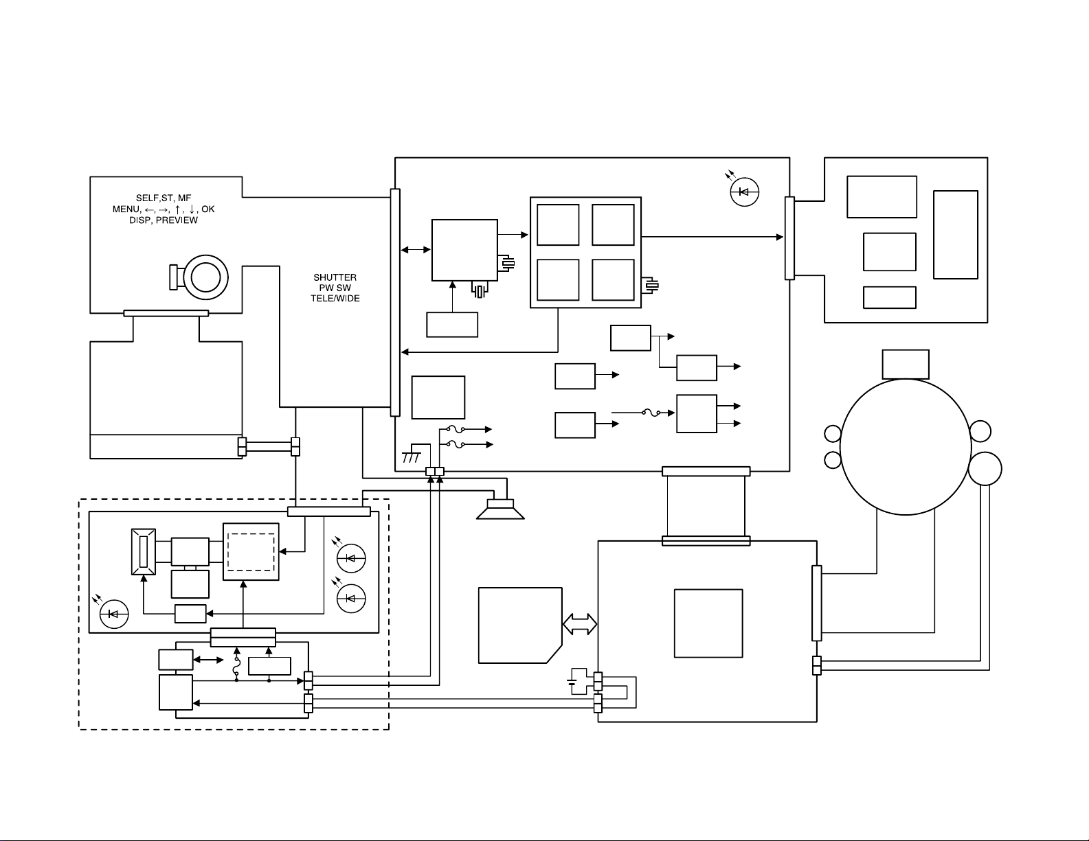
BLOCK DIAGRAM
Xe Lamp
Main
Capacitor
Trigger
Coil
Charging
Booster
IGBT
WhiteWhite
USB
DC in
ADP
Detection
AF assisist
lamp
G
R
PENTAX
Lens Unit
x 3
M
M
ZOOM
M
Finder
Rotary
SW
K-FPC
MIAN-PCB
SUB-PCB
C-FPC
76CMCM2
HJ936201BP
SD
Motor Driver
LB 8649RN
B to B
40 pin
40 pin
60 pin
22 pin
30 pin
Li-Batt
3.3 V-4.2 v
Digital I/F LCD
VGH: 15.0 V
VSH: 5.0 V
VDD: 5.0 V
BL (LED X 3)
ST UNIT
VCC1-ST
BUZZER
VCC1-1
VCOM
Amp
TK17030M
BACK UP
Capacitor
76C FLASH
Timer LED
SDRAM SH
32 KHz
8 bit
Microprocessor
M37516M6H
VCC1-2
15 V
5 V
4.00 MHz
4.00 KHz
VCC1.5
VCC3.3
VCC1.2
VCC5
VCC3
VCC15
VCC7.5
R
DOWN
Converter
DOWN
Converter
UP
Converter
UP
Converter
REG
CDS/AGC+AD
HD49334ANP
1CX412AQ
COD
3Mpix
CD3440EN
TV7SZ04FU X 3
V. Driver
H. Driver
— 4 —
Page 7
TEST MODE
Note: Do not perform the menu item unless explained here. (It may damage the internal data and
camera becomes unusable.)
Booting
To boot the test mode
Turn the power on while pressing both "MENU" and "DISP" buttons.
The program version is displayed.
Press "RIGHT" button, "Right" button and "MENU" button while the program version is displayed.
MAIN MENU is dispalyed.
QV-R3 (as of July 3, 2002) QV-R4 (as of July 3, 2002)
++ KX861 ++
PR : 02.07.03.21.47
LD : 1.06
MI : 41
"Right" button, "Right" button, "MENU" button
1 :VERSION INFO
2 :VIDEO OUT
3 :USB TCC TEST
4 :TEST MENU
5 :BEEP TEST
6 :TASK-2 TEST
7 :ROM UPDATE
8 :ADJ TEST
9 :REC-INFO
10 :TEST SCRIPT
11 :LAST MEMORY
SET button
MENU button
++ KX862 ++
PR : 02.07.03.21.48
LD : 1.06
MI : 41
1 :KEY CHECK
2 :VOCM CHECK
3 :MEMORY CHECK
4 :COLOR CHECK
5 :UGAIN CHECK
6 :VGAIN CHECK
7 :MESSAGE CHECK
8 :LED CHECK
9 :SW&JACK CHECK
— 5 —
Page 8

■ HOW TO DELETE "Power on default settings"
To delete "Power on default settings" set by individual customers, clear the memory as follows.
Note;
It is impossible to recover the memory after it was cleared.
It is impossible to delete "Power on default settings" of the motion picture.
Procedure;
After formatting the memory, execute "LAST MEMORY CLEAR" in the TEST mode.
(1) Turn the power on in REC mode and press MENU key.
(2) Select Set Up and execute format.
(3) Turn the power off.
(4) Turn the power on while pressing MENU and DISP key.
(5) Press right side of SET key twice, and press MENU key.
(6) Select "11:LAST MEMORY" and press SET key.
(7) The following message appears.
LAST MEMORY CLEAR
START .....
PUSH OK KEY?
(8) Press SET key, and turn the power off.
(9) Turn the power on again.
(10) "Power on default settings" set by the customers have been deleted when the language setting menu
appears.
— 6 —
Page 9

PROGRAM VERSION UPGRADING
■ Introduction
Update the program using the memory card.
Note:
Make sure to use a fully charged battery.
MAIN PCB becomes unusable if power down or an error occurs during program transmission.
1. How to confirm the program version
■ The program version can be confirmed in the test menu (refer to the previous page).
■ Turn the power on while pressing MENU button.
The following program version also can be found.
Check the LCD display.
(Example)
VER 1.00
(As of July 3. 2002)
2. How to update the firmware
1. Prepare the memory card which contains the software for upgrading firmware in the root directory.
qv-r3.bin (QV-R3)
qv-r4.bin (QV-R4)
2. Insert the above memory card into the camera, and set the AC adapter or a fully charged battery in the
camera.
3. While pressing MENU, press power switch. Keep pressing MENU until “PROGRAM UPDATE” appears
in the camera LCD
• The following appears.
• The version for the firmware update software in the memory card appears at the bottom.
PROGRAM UPDATE
YES
NO
NEW VERSION IS
VER 1.00
4. Align the white cursor to ”YES” by the cross keys of and , and press SET.
• “NOW LOADING” appears in the LCD and the update starts.
5. “COMPLETE” appears after the update finishes.
— 7 —
Page 10

6. Remove the memory card after turning the power off once. Turn the power back on again while pressing
MENU, and check the version.
VER 1.00
• “VER 1.00” appears this time.
7. If the version is correct, turn the power off.
8. Finally, check the operation by recording, playing back and deleting an image.
3. How to restore the firmware
1. Prepare the following firmware restoration program and change its name as follows;
kx861r.hbn mercury.bin (QV-R3)
kx862r.hbn mercury.bin (QV-R4)
2. Copy the above file to the root directory in the memory card.
3. Insert the memory card into the camera.
4. Set the AC adapter or a fully charged battery in the camera.
5. Turn the power on while pressing the shutter release button.
The LED next to the optical finder changes from green/red blinks green blinks/red lights only red
lights.
6. When only the red LED lights, the firmware restoration is finished.
Remove the AC adapter or the battery and turn the power off.
7. Turn the power on again while pressing MENU and DISP buttons.
The firmware is successfully restored if the corresponding version appears next to “PR” of the test
menu.
PR:02.07.03.21.47 (QV-R3)
PR:02.07.03.21.48 (QV-R4)
8. Finally, start the camera normally to check the operation by recording, playing back and deleting an
image.
— 8 —
Page 11

ADJUSTMENT
■ Introduction
Make sure to perform the adjustment when replacing the lens unit or the MAIN PCB.
The necessary software, driver and setting are explained in using USB ADJ Tool "adj331e.exe (Ver.1.1).
Note that the tool, drivers etc. are available only for Windows.
1. How to use USB ADJ Tool
1-1. Prepare the necessary software, driver and DLL file.
(1) Prepare the following three files.
• Commom test driver for CASIO/PENTAX
[testmode_pentax_casio] folder uusbd.dll
uusbd.inf
uusbd.sys
• ADJ data read/write tool "adj331e.exe"
• Commom DLL for USB test "uusbd.dll"
(2) Place the commom test driver for CASIO/PENTAX in an appropriate place.
(3) After downloading the common DLL for USB test, copy it to the same directory as that of the ADJ data
read/write tool or under "c:windows/system.
1-2. Set the camera so that it recognises the USB test mode.
(1) Enter the test mode and then the initial test selection screen.
Turn the power on while pressing both "MENU" and "DISP".
Press "RIGHT", "RIGHT" and "MENU.
(2) Move the cursor to "3:USB TCC TEST" and press "SET".
(3) Move the cursor to "1:USB TCC ON" and press "SET".
(4) Press "MENU" button and leave the test mode.
(5) This enables the camera to recognise the USB test mode flag.
(6) When the USB test mode flag is ON, the test menu appears first when the camera power is turned on.
* If the USB test mode flag should be OFF, set "2: USB TCC OFF" in the test menu.
1-3. Install the USB driver for the USB test mode in the computer.
(The following is an example using the Windows Me.)
(1) Prepare the USB driver for the USB test mode.
(2) Turn the camera power on which is set in the USB test mode and let it enter the USB test mode as
shown in 2.(the test menu appears right after the power is turned on).
(3) Connect the camera in the above status to the computer by the USB cable.
(4) "A wizard for the new hardware" appears.
(5) Check "Designate the place for the driver (for users with sufficient knowledge)" and press "Next".
(6) Check "Search for the optimum driver for the device (recommended)".
(7) Check "Designate the place to search" , designate the place which contains "inf" file in the driver by
pressing "Reference" button, and then press "Next" button.
(8) When "Universal USB Driver (VMEM manufacturer's name)" appears upon message "Searching for
the driver file for the following devices" , press "Next" button.
(9) The file copy starts.
(If a message "uusbd.Inf cannot be found" appears during the file copy, designate the same place as in
the step 7).
(10) Press "Complete" button.
(11) Right-click "My computer", select "Property" and open "Device manager". If "Universal USB Driver
(VMEM manufactur's name)" can be found in "USB device for UUSBD", the computer has successfully
recognised the driver.
(12) The test driver can be used for both CASIO/PENTAX. Installing the test driver into either one enables
the other one to recognise it.
— 9 —
Page 12

NOTE: How to uninstall the USB driver for the USB test mode
• Connect the camera while in the USB test mode to the computer so that the computer recognises the
camera.
• Right-click "My computer", select "Property" and open "Device manager".
• Select "USB device for UUSBD" , and then "Universal USB Driver (VMEM manufacturer's name)".
• Press "Delete" button and delete the driver.
• When using Windows98/98SE/Me, delete the following three files;
(NOTE! Do NOT delete "usbd. inf" and "usbd.sys", whose names are much alike the following.)
C:windows / inf / uusbd.inf
C:windows / inf / other / KashiwanoUUSBD.inf
C:windows / system32 / drivers / uusbd.sys
• The driver has been successfully deleted.
1-4. Use the USB ADJ Tool
(1) Prepare ADJ data read/write tool "adj331e.exe".
(2) Copy the common DLL for USB test to the same directory as that of the ADJ data read/write tool
"adj331e.exe" or under "c:windows / system".
(3) Turn the camera power on which is set in the USB test mode and let it enter the USB test mode (the test
menu appears right after the power is turned on).
Connect the camera to the computer by the USB cable.
(4) Boot "adj331e.exe." and use it as follows;
• Read ADJ data from the camera. Press "read from the camera".
• Write ADJ data into the camera. Press "write into the camera".
• Save ADJ data which is read. Press "File" and "Save", and save it with an appropriate name.
• Open ADJ data which is saved. Press "File" and "Open", and open the necessary file.
— 10 —
Page 13

2. Lens Replacement
Make sure to perform the following procedure after replacing the lens.
A foppy disk with the lens data is bundled in the spare parts of the lens unit.
1 Enter the TEST mode.
1. Turn the power on while pressing both "MENU" and "DISP" buttons.
2. Press "RIGHT" button, "RIGHT" button and "MENU" button while the
program version is displayed.
3. Select "3.USB TCC TEST".
4. Select "1. USB TCC ON".
5. Turn the power OFF.
2 Turn the power ON and connect QV to the computer by the USB cable.
3 Boot "adj331e.exe" .
4 From "File/Open" , open the bundled floppy disk.
5 Click "WRITE" button of "ADJ ALL".
6 After adjustment, change "1. USB TCC ON" to "2. USB TCC OFF".
3. MAIN PCB Replacement
Make sure to backup ADJ DATA before replacing the MAIN PCB.
IMPORTANT NOTICE:
The MAIN PCB is a common part for QV-R3 and QV-R4 as a spare part.
After replacing MAIN PCB, firm up and system initialization should be required.
Refer to the service bulletin QV-069.
4
5
1 Enter the TEST mode.
1. Turn the power on while pressing both "MENU" and "DISP" buttons.
2. Press "RIGHT" button, "RIGHT" button and "MENU" button while the program version is displayed.
3. Select "3.USB TCC TEST".
4. Select "1. USB TCC ON".
5. Turn the power OFF.
2 Turn the power ON and connect QV to the PC by the USB cable.
3 Boot "adj331e.exe" .
4 Click "ADJ ALL READ", and display the information on the computer screen.
5 Save the information in the computer.
6 Replace the MAIN PCB.
7 Perform the above 1 to 3 after replacing the MAIN PCB without any problem.
8 Open the file which is saved above.
9 Click "WRITE" button of "ADJ ALL".
0 After adjustment, change "1. USB TCC ON" to "2. USB TCC OFF".
5 8
4
9
— 11 —
Page 14

4. Operation and Current consumption
1. Operation check
1 Unti-shock, Battery operations, AC adaptor operations
2 Switch, buttons operations
3 CF CARD insersion/eject operation, battery cover open/close operation
4 Resolution and color repeatability check
5 AE operation, AF function, zoom operation
6 USB function check
7 Dust and scratches on lens
8 Appearance check
9 Optical zoom finder check
2. Current consumption test
Current consumption (DC IN = 4.5 ± 0.1 [V])
• Make sure that current consumption is less than 300 mA in PLAY mode.
• Make sure that current consumption is less than 470 mA in REC mode.
• Make sure that current consumption is less than 4 mA when power is turned OFF.
• Make sure that current consumption is less than 1300mA when the strobe is charged.
3. Change in the indication of the battery mark
Check that the indication of the battery mark changes as shown below in the PLAY mode.
DC IN = 4.50 ± 0.05 [V]
DC IN = 3.85 ± 0.05 [V]
— 12 —
Page 15

5. Assist light adjustment
1. General
Perform this adjustment when the assist light reflected on the object is not in the focus range.
2. Necessary equipment.
(1) Dark room.
(2) SD card or MMC card.
(3) Script file "autorun.scp", which is on the service CD-ROM.
3. Condition.
(1) Perform the adjustment in a dark room.
(2) Distance between Lens unit and object is 2.0 ± 0.1m.
(3) The camera's front case is removed.
4. Procedure.
(1) Copy "autorun.scp" to a root directory of an SD/MMC card.
(2) Insert the SD/MMC card to the camera.
(3) Turn on the camera in the REC mode.
(4) Assist light comes on.
(5) Turn the screw(as shown below) and move the assist light reflected on the screen into the focus
range.
(6) After adjustment, turn off the camera.
5. Adjustment process
Focus range Adjusted
Assist light reflected on the screen.
— 13 —
Page 16

DISASSEMBLY
NOTE:
There are 10 kinds of screws.
It would be convenient to have a case for storing screws when disassembling.
1. Remove the battery pack.
2. Remove three screws (S1) and screws (S9 and S10).
Screw (S9)
Screw (S1)
Screw (S1)
3. Open the REAR CASE half way as shown below.
After removing the FPC, remove the REAR CASE.
FPC
Screw (S10)
Screw (S1)
NOTE:
Slide the slide switch of the finder to the
left before assembling.
— 14 —
Page 17

4. Remove the jack cover.
5. Remove three screws (S1) and two screws (S8).
Screws (S8)
Screws (S1)
6. Loosen the screw (S1) and remove the FRONT CASE.
NOTE:
Be careful of the KEY PCB when fixing the
FRONT CASE.
Screw (S1)
— 15 —
Page 18

7. Remove the screw (S1) and then the TRIPOD SCREW.
8. Remove the screw (S9) and then the CENTER CASE and the POWER BUTTON.
Screw(S9)
9. Disassembling the LCD UNIT
1 Remove the connector.
Remove the screw (S7) and the screw (S6).
2 Remove the LCD FRAME.
3 Remove the LCD FRAME.
4 Remove the connector and the LCD UNIT.
123
Screw(S6)
Connector
FRAME
4
Screw(S7)
Connector
FRAME
NOTE:
Hold the connector tightly and remove the LCD UNIT.
— 16 —
Page 19

10. Remove the screw (S5) and then the STRAP.
Screw(S5)
11. Disassembling the MAIN PCB
1 Unsolder two wires (blue and white).
2 Remove the connector.
3 Remove two screws (S4) and two screws (S7).
4 Remove the MAIN PCB.
1
23
Screws (S4)
Connector
Screws (S7)
4
NOTE:
Be careful not to pinch the wire (black) when fixing the
MAIN PCB.
— 17 —
Page 20

12. Disassembling the KEY PCB
1 Remove the screw (S4).
2 Remove the KEY PCB, which is attached by double-sided tape.
3 Remove the KEY PCB from the connector.
123
Screw(S4)
NOTE:
Be careful of the spring, which can be easily removed.
Make sure to fix it again when assembling.
13. Disassembling the strobe unit
1 Remove the screw and screws (S4 and S3).
Screw Screw(S4) Screw(S3)
2 Remove the condenser, which is attached by double-sided tape.
NOTE:
Before discharge, be careful not to touch the terminals of the condenser.
— 18 —
Page 21

3 Remove the KEY PCB, which is attached by double-sided tape.
Remove the connector.
double-sided tape double-sided tape
4 Discharge the condenser for the strobe.
Connector
5 Unsolder two wires (orange and gray).
WIRE (gray)WIRE (orange)
— 19 —
Page 22

14. Remove the screw (S7) and two screws (S6) and then the chassis.
Screw(S7)
Screws (S6)
Remove two fittings for holding the screws.
15. Disassembling the SUB PCB
1 Unsolder the wires (two red and two black).
NOTE:
Be careful not to lose the fittings for the screws
when removing the Chassis.
RED WIRE
BLACK WIRE
2 Remove two screws (S4) and two connectors.
— 20 —
RED WIRE
BLACK WIRE
Screws (S4)
Connectors
Page 23

2 Remove the SUB PCB.
16. Disassembling the lens unit
1 Remove two screws (S6).
Screws (S6)
2 Remove the lens unit.
NOTE:
Fix the lens unit into the hook tightly when assembling.
Hook
— 21 —
Page 24

17. SD CARD COVER
1 Remove the COVER SPRING.
2 Remove the shaft.
18. Disassembling the BATTERY COVER
1 Remove the shaft.
2 Remove the BATTERY COVER.
— 22 —
Page 25

EXPLODED VIEW
S9
S1
8
S1
S5
29
34
S4
S4
x 2
30
25
24
38
16
S9
23
45
46
20
x 4
S6
22
21
x 2
41
42
43
44
39
40
S2
47
37
x 2
S3
x 2
10
11
32
S4
15
12
17
9
48
S1
13
14
15
S4
S3
31
S4
S10
S7
S6
4
6
5
7
35
36
S7
S4
x 2
18
33
19
23
26
28
— 23 —
S1
S7 x 2
2
S8 x 2 S1
x 2
S6
3
S1 x 2
1
S2 x 3
Page 26

PARTS PRICE LIST
QV-R3/R4
N Item Parts Code Parts Name Specification Price R Remark
1 1008 7872 CASE ASSY / FRONT RJK503326*001V01TK 1 0 CQ A
1 1008 7873 CASE ASSY / FRONT RJK503326*002V01TK 0 1 CQ A
2 1008 6339 CAM RING A-K861 RJK502902-001V01 1 1 BH X
3 1008 6340 TRIPOD SCREW RJK502903-001V01 1 1 AI X
N 4 1009 2334 LENS UNIT K861 RJK503657*001V01TK 1 0 EK A
N 4 1009 2335 LENS UNIT K862 RJK503657*002V01TK 0 1 EM A
5 1008 5349 BL UNIT LBL-K861 1 1 BX A
6 1008 3214 LCD UNIT COD16T1048ED 1 1 CR A
7 1008 6354 HARNESS CN036PC30097 1 1 AE X
8 1008 7874 CASE ASSY / REAR RJK503327*001V01TK 1 1 CH C
9 1008 6350 MODE BUTTON A-K861 RJK502878-001V01 1 1 AH C
10 1008 6353 SW UNIT UBF013L01A 1 1 CC A
11 1008 6345 CS FRAME A-K861 RJK502856-001V01 1 1 AC X
12 1008 6347 ENTER KEY A-K861 RJK502858-001V01 1 1 AE C
13 1008 6346 CS BUTTON A-K861 RJK502857-001V01 1 1 AE C
14 1008 6349 MENU BUTTON A-K861 RJK502877-001V01 1 1 AE C
15 1008 6348 LCD BUTTON A-K861 RJK502876-001V01 2 2 AE C
16 1008 6311 PCB ASSY / KEY KX-0861-PKA P 1 1 CD A
17 1008 6393 PCB ASSY / MAIN KX-0861PMA P 1 1 DT A
18 1008 6316 PCB ASSY / SUB KX-0861-PSA P 1 1 BV A
19 1008 6319 FRAME A-K861 RJK502886-001V01 1 1 AQ X
20 1008 6418 ADHESIVE TAPE D-K861 RJK502957-004V01 4 4 AA X
21 1008 6318 KNOB / BATTERY RJK502872-001V01 1 1 AC X
22 1008 6323 SPRING C / BATTERY RJK502934-001V01 1 1 AA C
23 1008 6322 SHAFT C-K861 RJK502914-001V01 2 2 AA X
24 1008 6363 SPRING A / BATTERY RJK502867-001V01 1 1 AA C
25 1008 6364 SPRING B / BATTERY RJK502868-001V01 1 1 AA C
26 1008 6317 SD SPRING A-K861 RJK502866-001V01 1 1 AA C
27 1008 6320 SHAFT A-K861 RJK502912-001V01 1 1 AA X
28 1008 7875 ASSY / BATTERY COVER RJK503065*001V01TK 1 1 AW A
29 1008 7876 ASSY / SD COVER RJK503064*001V01TK 1 1 AV A
30 1008 6321 SHAFT B-K861 RJK502913-001V01 1 1 AB X
31 1008 6373 STROBE UNIT STB0180AD04QE677 1 1 CS A
32 1008 6277 SUB ASSY / CENTER CASE RJK502929*001V01 1 1 AX A
33 1008 6307 CHASSIS B-K861 RJK502916-001V01 2 2 AA X
34 1008 6304 PIN / STRAP A-K861 RJK502904-001V01 1 1 AH X
35 1008 6303 LCD FRAME A-K861 RJK502871-001V01 1 1 AB X
36 1008 6305 LCD FRAME B-K861 RJK502905-001V01 1 1 AA X
37 1008 6300 TAPE A-K861 RJK503455-001V01 2 2 AA X
38 1008 6290 SPRING / BATTERY B-K861 RJK503370-001V01 1 1 AA X
39 1008 6356 KNOB / ZOOM K861 RJK502899-001V01 1 1 AI C
40 1008 6360 SPACER A / SHATTER RJK502938-001V01 1 1 AA X
41 1008 6361 SHATTER PANEL A-K861 RJK502939-001V01 1 1 AN X
42 1008 6362 ADHESIVE TAPE SH-K861 RJK502960-001V01 1 1 AA X
43 1008 6355 SHATTER BUTTON A-K861 RJK502881-001V01 1 1 AC C
44 1008 6358 SPRING A / SHATTER RJK502935-001V01 1 1 AA X
45 1008 6357 SHATTER FRAME A-K861 RJK502919-001V01 1 1 AA X
46 1008 6359 SPRING B / SHATTER RJK502936-001V01 1 1 AA X
47 1008 6281 POWER BUTTON A-K861 RJK502882-001V01 1 1 AF X
48 1008 6280 COVER / CONNECTOR A-K861 RJK502850-001V01 1 1 AD C
Notes : N : New registration parts
Q : Quantity used per unit
R : Rank
QTY
QV-R3 QV-R4 Code
- 24 -
Page 27

N Item Parts Code Parts Name Specification Price R Remark
S1 1008 6282 SCREW RJK502970-001V01 7 7 AA X
S2 1008 6342 SCREW S-1PMA-1.4X1.4BCME 5 5 AA X
S3 1008 6352 SCREW S-1FMA-1.7X3.0BCME 3 3 AA X
S4 1008 6302 SCREW S-3PBT-1.4X3.5NI 9 9 AA X
S5 1008 6301 SCREW S-3FBT-1.4X3.0NI 1 1 AA X
S6 1008 6308 SCREW S-3PBT-1.7X4.0BC 5 5 AA X
S7 1008 6309 SCREW S-3PMA-1.7X2.5BCME 4 4 AA X
S8 1008 6283 SCREW / FLAT RJK502970-002V01 2 2 AA X
S9 1008 6285 SCREW / FLAT RJK502971-001V01 2 2 AA X
S10 1008 6284 SCREW / FLAT RJK502970-003V01 1 1 AA X
ACCESORY
- 1009 0415 BATTERY / LITHIUM ION NP-30-E 1 1 CR B
- 1009 0412 STRAP ST-K861 1 1 AF X
- 1009 0416 CHARGER (JU) BC-20-WW-JU 1 1 CH X USA *1
- 1009 0417 CHARGER (EU) BC-20-WW-EU 1 1 CI X EURO *2
- 1009 0418 CHARGER (UK) BC-20-WW-UK 1 1 CL X UK *3
- 1009 0419 PLUG / AC(JU) PLG-K861-AC-JU 1 1 AG X USA
- 1009 4508 PLUG / AC(EU) PLG-K861-AC-EU 1 1 AK X EURO
- 1009 4509 PLUG / AC(AS) PLG-K861-AC-AS 1 1 AU X AUSTRALIA
- 1010 3431 PLUG / AC(KC) PLG-K861-AC-KC 1 1 AN X KOREA
- 1009 0421 USB CABLE UC-K861-LG10 1 1 AQ X
- 1009 0423 CD-ROM CK861DCA01R 1 1 AI X
Notes : N : New registration parts *1 : USA PLUG is attached.
Q : Quantity used per unit *2 : EURO PLUG is attached.
R : Rank *3 : UK PLUG is attached.
QTY
QV-R3 QV-R4 Code
- 25 -
Page 28

PRINTED CIRCUIT BOARDS
MAIN PCB
TOP VIEW
— 26 —
Page 29

MAIN PCB
BOTTOM VIEW
— 27 —
Page 30

SUB PCB
TOP VIEW
BOTTOM VIEW
— 28 —
Page 31

KEY PCB
— 29 —
Page 32

MAIN PCB
RESETP
IRQ4
FOUT
IRQ5
PSOUT
DREQ0
PSIN
KINTB
PSCK
GLED
RLED
SHUTTER2
SELFLED
BUZZER+
BUZZER-
AFLEDK
DPLUS
DMINUS
R420
0
TH1
AFPIDET
SHUT1
CP400
VIDEO
CHGN
CENDN
Q402
DTC144EETL
3
1
GND
VCC5-3
3
1
GND
SELF
BLCTL
L_PWM
2
L420
47u
R416
J1K
Q400
DTC114EETL
SCHEMATIC DIAGRAMS
WATCH
PSRDY
USBRDY
STATUS0
STATUS1
R419
J47K
VCC1.5
VCC3-1
L400
10u
C400
6.3V33(A)
C401
6.3V33(A)
307
VSS
308
MD6
309
RESETP
310
USB_VBUS
311
CA
312
IRQ4
313
RTCEXTAL
314
MD3
315
IRQ5
316
RTS2
317
RTCXTAL
318
MD4
319
VSS
320
RXD0
321
VDD
322
VSSUSB
323
C402
0.1u
SDRXD2
C403
0.1u
R400
J47K
CD9
CD8
CD7
CD2
CD1
CD3
CD0
CD4
R402
D5.1K
CD5
C404
SDWP
SDCLK
SDDAT0
SDDAT3
BUZZER
SDDET
C420
0.1u
SDDET
CD6
SHD
SHP
HB(H2)
H(H1)
FR
B0.1u
C406
0.1u
R404
C407
0.1u
R405
R406
R407
R408 0
C408
0.1u
GND
R418
F180
2
RVSS
324
VDD
325
RXD2
326
VSS
327
VSS
328
DM
329
RVDD
330
DREQ0
331
VSS
332
TXD0
333
VDDPLL1
334
DP
335
USBXTAL
336
DREQ1
337
VDD
338
SCK0
339
VSSPLL1
340
VDDUSB
341
USBEXTAL
342
VSS
343
AN3
344
AN2
345
AN1
346
CCDDT9
347
CCDDT8
348
CCDDT7
349
CCDDT2
350
CCDDT1
351
AN0
352
CD5
353
CD2
354
VDDP
355
CCDDT3
356
CCDDT0
357
CCDSG1
358
CD6
359
CD3
360
CD0
361
CCDDT4
362
CCDSG3
363
REXT2
364
R401
VDDP
365
0
CD4
366
CD1
367
CCDDT5
368
CCDSG2
369
CBU2
370
EXTCCLK
371
AVSS
372
AVDD
373
AVDD
374
AVSS
375
VIDEO
376
CFWAITB
377
CFRDY
378
CFCD2
379
CCDDT6
380
EXSCR
381
VBB
382
VDDTG
383
VSS
384
D_PULS
385
D_MINUS
386
LTTRG
387
SHUTCTR
0
388
SHD
389
CFIOWRB
390
CFCD
391
VDD
392
CDSHD
393
VDD
394
0
SHP
395
FH1
396
0
VDD
397
PWM1
398
CDSVD
399
VSSTG
400
0
FH2
401
CFIORDB
402
PWM2
403
CD7
404
FR
405
CFRST
406
VDDP
407
CFRDB
408
EXINT2
R417
J47K
CP401
GND
R415
J75
3
1
GND
CDSCK
SDSCK
SDTXD2
303
306
304
305
302
CS0
PTC3
PTC6
SCK2
B23
A23
B22
A22
B21
A21
B20
A20
B19
A19
B18
A18
B17
A17
B16
A16
B15
A15
B14
A14
B13
A13
B12
A12
B11
A11
B10
A10
B9
A9
B8
A8
B7
A7
B6
A6
B5
A5
B4
A4
B3
A3
B2
A2
B1
A1
VSS1EXINT12CFCE1B3XTAL14CFWRB5CFREGB6EXTAL17VSSPLL08IVDD9CFCE2B10XTAL311VDDPLL012VDD13BUZZER14VSS15EXTAL316D3017PCMLRCK18PCMCLK19PCMSCK20VSS21D2922D2823EXCSCK224D2725D2626VDD27D2128D2229D2330D2431D2532VSS33D2034D1935D1836D1737D1638VDDP39D1240D1341D3142D1443D1544VSS45D1146D1047D948D849D750VDDP51D252D353D454D555D656VSS57D158D059SDCASB60SDRASB61SDDQM3B62SDDQM2B63SDCSB64SDWEB65EXINT366TE267SDDQM0B68SDDQM1B69EXCCKIO170A071A172A273A374A475A1076A977A878A779A680A581A1182VDDP83A1284A1385VSS86A1487A1588A1989A2490IRQ291EXCIRL2B92A1693A2094A2595PCMDO96A1797A2198PCMDI99VDDP
SDCMD
Q401
DTC143EETL
AFLIGHT
2
301
TXD2
SDDAT2
PTD7
C23
C22
C21
C20
C19
C18
C17
C16
C15
C14
C13
C12
C11
C10
C9
C8
C7
C6
C5
C4
C3
C2
C1
300
NAIO7
SDDAT1
C418
0.1u
285
289
291
292
293
294
295
296
298
299
NAIO6
NAIO5
297
PTD1
NAIO4
D23
D22
D21
D20
D19
D18
D17
D16
D15
D14
D13
D12
D11
D10
D9
D8
D7
D6
D5
D4
D3
D2
D1
286
287
288
290
VSS
VSS
VDD
VDD
NAIO0
NAIO1
NAIO2
NAIO3
R409
J1M
STATUS0
STATUS1
E23
F23
E22
F22
E21
F21
E20
F20
E19
F19
E18
F18
E17
F17
E16
F16
E15
F15
E14
F14
E13
F13
E12
F12
E11
F11
E10
F10
E9
F9
E8
F8
E7
F7
E6
F6
E5
F5
E4
F4
E3
F3
F2
E2
E1
F1
CP403
TP0
H400
1 2
13.5MHZ
R410
J220
VDDP
C409
CH15p
C410
CH15p
284
VSS
R414
J47K
282
281
283
RESETM
ASEBRKAK
R411
J47K
C417
0.1u
CDSCS
279
276
277
275
280
274
278
VSS
TDO
TMS
MD5
TCLK
EXTAL
AUDCK
ASEMDO
G23
H23
G22
H22
G21
H21
G20
H20
G19
H19
G18
H18
G6
H6
G5
H5
G4
H4
G3
H3
G2
H2
G1
H1
C411
0.1u
PSRSTB
SHUTDLY
AFANODEN
XV3
268
273
271
272
TCK
CTS2
VDDP
J23
J22
J21
J20
J19
J18
261
270
TDI
260
267
264
259
265
266
262
263
269
VSS
VSS
XV3
NMI
PTE7
TRST
PTM0
PTM1
PTM3
VDDP
NARST
K23
L23
K22
L22
K21
L21
K20
L20
K19
L19
K18
L18
257
258
FL_ANRST
IGBTG
CH3
XV2
ADCLK
R413
J47K
CDSDATA
247
255
253
254
256
VSS
PTJ4
PTM2
NACDE
NARYBY
M23
M22
M21
M20
M19
M18
243
249
252
244
248
246
245
241
250
NAWE
251
NAOE
NACE1
N23
N22
N21
N20
N19
N18
IGBTN
ADCLK
NASC
AUDATA3
AUDSYNC
P23
P22
P21
P20
P19
P18
240
242
XV2
PTJ3
PREN
d_s_APT
R23
R22
R21
R20
R19
R18
IC400
76C MCM1
HJ932601BP
TopView
2001.09.07
M6
K6
J6
J5
J4
J3
J2
J1
L6
K5
L5
K4
L4
K3
L3
K2
L2
K1
L1
C412
0.1u
N6
P6
R6
M5
N5
P5
R5
M4
N4
P4
R4
M3
N3
P3
R3
M2
N2
P2
R2
M1
N1
P1
R1
239
CH3
238
AUDATA1
AUDATA0
DACK0
BACK
USBCNT
CLK
XV1
CH4
CH2
CH1
OFDC
XV4
228
DACK0
PBLK
224
227
222
225
226
221
223
220
219
XV4
MD7
PTE3
PBLK
OFDC
VDDP
BACK
MCKE
MCLK
W23
V23
W22
V22
W21
V21
W20
V20
W19
V19
W18
V18
W17
V17
W16
V16
W15
V15
W14
V14
W13
V13
W12
V12
W11
V11
W10
V10
W9
V9
W8
V8
W7
V7
W6
V6
W5
V5
W4
V4
W3
V3
W2
V2
W1
V1
CLPOB
237
231
233
232
230
229
234
235
236
VSS
CH1
CH2
CH4
XV1
PTE1
CLPOB
CLPDM
AUDATA2
T23
U23
T22
U22
T21
U21
T20
U20
T19
U19
T18
U18
T6
U6
T5
U5
T4
U4
T3
U3
T2
U2
T1
U1
RESETP
0.1u
C416
217
218
216
CKE
VDDR
SDTCK
Y23
Y22
Y21
Y20
Y19
Y18
Y17
Y16
Y15
Y14
Y13
Y12
Y11
Y10
Y9
Y8
Y7
Y6
Y5
Y4
Y3
Y2
Y1
SUB
VCC1-1
IC453
4
OUT
VSS
3
VDD
NC
S-80832CNNB
R472
D300K
R461
J330
R462
F20K
R463
F75K
0.1u
GND
C459
BEND1
1
2
EX-BUS(11)
212
208
205
207
210
209
215
211
213
206
SDTDI
214
VSSR
CP404
TP1
SDTDO
SDTRST
AA23
AA22
AA21
AA20
AA19
AA18
AA17
AA16
AA15
AA14
AA13
AA12
AA11
AA10
SDTMS
AA9
AA8
AA7
AA6
AA5
AA4
AA3
AA2
AA1
VSS
VDDP
SDRESET
VSS
VSS
SUB
AB23
AC23
204
SCR
203
C415
0.1u
202
201
200
FRP
BL
CLR
OE
VSS
TE1
TE0
CS4
VSS
CS5
CS6
VSS
VSS
VSS
VSS
VSS
VSS
VSS
A23
A18
VSS
FRP
199
GRES
198
197
STH
196
D02
195
194
193
192
191
190
189
188
187
186
185
184
183
182
181
180
179
178
177
176
175
174
173
172
171
170
169
168
167
166
165
164
163
162
161
160
159
158
157
156
155
154
153
152
151
150
149
148
147
146
145
144
143
142
141
140
139
138
137
136
135
134
133
132
131
130
129
128
127
126
125
124
123
122
121
120
119
118
117
116
115
114
113
112
111
110
109
108
107
106
105
104
103
SHUT0
ZC1
GSRT
STB
D03
GPCK
AF3
D01
D05
D04
POL
ZC2
AF2
USBRDY
ZC0
D00
ZOOM1
ZOOM0
C414
0.1u
CP
MVC2
MVC1
AF1
AF0
DREQ0
IRIS1
IRIS0
C419
OPEN
RESETB
STATUS1
STATUS0
IRQ4
DACK0
RESETP
BACK
EXCOS
IRQ5
C413
0.1u
SHUTTER
LCDFD1
VBUSCNT
LCDFD0
LCDCP
VBBENB
EXCBREQB
EXCDREQ0B
EXCCS4B
RESETB
EXCSTATUS1
EXCSTATUS0
EXCIRQ4B
EXCDACK0B
EXCCS5B
EXCRESETPB
EXCBACKB
EXCOS
EXCRDB
EXCBSB
EXCIRL1B
EXCCS6B
EXCDREQ1B
NORCE
EXCWAIT0B
EXCIRQ5B
EXCIRL3B
EXCIRL0B
VDDP
VDDP
GRES
VSSR
VDDP
VSSR
VDDR
VSSR
MPZ3
GSRT
GPCK
HCNT
MPF3
VDDR
VDDR
VSSR
VDDR
MPF2
MPZ2
MPZ1
MPZ0
VDDR
VDDR
VSSR
VSSR
BREQ
MPF1
MPF0
VDDP
VDDP
VDDP
WE1B
WAIT
VDDP
VDDP
VDDP
WE0B
PTD3
SRTL
MPI3
RSV1
RSV2
MPI2
MPI5
MPI4
MPI1
MPI0
RDB
IRQ1
EXH
IRQ3
IRQ0
AB22
AC22
AB21
AC21
AB20
AC20
AB19
AC19
AC18
AB18
AB17
AC17
AB16
AC16
AC15
AB15
AB14
AC14
AB13
AC13
AB12
AC12
AB11
AC11
AB10
AC10
AC9
AB9
AB8
AC8
AB7
AC7
AB6
AC6
AB5
AC5
AB4
AC4
AB3
AC3
AB2
AC2
AB1
AC1
A22
VSS
100
101
102
CP405
TP2
EVCC3.3
ADPTN
R475
J100K
32
1
R474
D120K
BATTERY
GND
KIN4
KIN3
KIN2
KIN1
KIN0
R460
F10K
R458
F10K
R459
F10K
0.1u
C460
EVCC3.3-0
R469
J100K
PWSW
R468 J100K
Q453
2SD2216J-R(TX)
R470
J1M
R471
C464
0.01u
C461
B2700p
R467 J100K
BEND2
EVCC3.3
C450
J1M
C465
0.01u
USBCONB
KINTB
WATCH
31
33
30
32
0.1u
P00/SIN2
34
P35/AN5
P02/SCLK2
P01/SOUT2
35
P34/AN4
36
P33/AN3
37
P32/AN2
38
P31/AN1
39
P30/AN0
40
VCC
41
VREF
42
AVSS
43
P45
44
P44/INT3
IC450
M37516M6H
P43/INT21P42/INT12P41/INT03P40/CNTR14P27/CNTR0/SRDY15P26/SCLK6P25/SCL2/TXD7P24/SDA2/RXD8P23/SCL19P22/SDA110CNVSS
R466
J47K
PSRSTB
RESETB
29
P03/SRDY2
8bit
PSRDY
EXCOS
PSCK
PSOUT
PWCTL0
P0726P0627P0528P04
PSIN
PWCTL1
25
SHUTTER2
FOUT
STATUS0
BLCTL
PWCTL3
P12/LED223P11/LED124P10/LED0
P13/LED3
P14/LED4
P15/LED5
P16/LED6
P17/LED7
RESETB
P20/XCOUT
P21/XCIN
11
VPPCTL
XOUT
22
SHUTSW2
21
SHUTSW1
20
19
18
17
VSS
16
15
XIN
14
13
12
LCD-BUS(16)
CCD-BUS(31)
KEY-BUS(14)
PWCTL-BUS(5)
(FULL)
(HALF)
H451
3
1
CERALOCK
BEND0
R453
J3.3M
R454
J620K
1 2
H450
32KHz
C453
C452
CH15p
CH18p
2
3
INB1INA
GND
IC451
TC7SET08FU
OUTY4VCC
5
JK-BUS(5)
MD-BUS(19)
ST-BUS(3)
2
C451
0.1u
VCC3-1
SD-BUS(11)
VCC5-1
C456
OPEN
R473
J47K
2
VDD
CD3OUT
C454
B2700p
1
4
MAIN2
MAIN2
MAIN2
MAIN2
MAIN2
MAIN2
MAIN2
Q452
OPEN
2 3
OPEN
R457
1
3
2
1
GND
VSS
IC452
S-80927CLNB
C455
0.1u
MAIN2
C457
OPEN
Q451
OPEN
R465
J22
C462
PAS621L-VL3
R456
J100K
C463
PAS621L-VL3
— 30 —
Page 33

MAIN1
MAIN1
MAIN1
MAIN1
MAIN1
MAIN1
ST-BUS(3)
JK-BUS(5)
SD-BUS(11)
KEY-BUS(14)
LCD-BUS(16)
MD-BUS(19)
AFANODEN
AFANODE
AF3
AF2
AF1
AF0
MVC2
MVC1
ZC2
ZC1
ZC0
TH1
AFANODE
AFPIDET
R364
J10K
3
1
VCC3-1
1
F24
2
Q362
DTC144EETL
EVCC3.3
Q361
2SJ347
GND
3 2
R361
USB
J1.5K
3
1
VCC3-1
R360
J47K
USBVCC
2
Q360
DTC144EETL
DP
DM
R365
J470K
CENDN
IGBTG
DM
DP
USBVCC
CHGN
C328
0.1u
SDDET
SHUTSW2
SHUTSW1
FRP
VCC5L
L_PWM
VCOM_DC
2SD2216J-R(TX)
VCC15
VCC5L
IC330
R334
1
8
A.IN-
A.OUT
J36K
2
7
A.IN+
R335
J36K
GND
R321
J1M
2
VCC
3
B.IN+
GND
4
B.IN-
B.OUT
TK17030M
Q320
SI1013R
L320
2 3
1
3
Q321
1
DTC144EETL
6
5
100u
R333
D8.2K
R332
D5.1K
VCC5-3
R320
J100K
R330
J10K
321Q330
VCC3-1
1
Q310
DTA123JETL
2
3
R311
J100
SHUTDLY
SHUT1
SHUT0
ZOOM1
ZOOM0
VCC3-1
VCC3-1VCC5-2
81
RM310
J47K
4 5
3 6
SHUTDLY
IRIS1
IRIS0
SHUT1
SHUT0
ZOOM1
ZOOM0
2 7
1
GND
2
3
IRIS1
4
IRIS0
5
6
7
8
9
GND
10
DAT2
11
DAT3
12
CMD
13
CLK
14
DAT0
15
DAT1
16
CDET
17
CWP
18
19
GND
20
GND
C311
0.1u
CN310
WR-40SB
Top View
40
GND
39
GND
38
AF3
37
AF2
36
AF1
35
AF0
34
MVC2
33
MVC1
32
GND
31
VCC5-2
30
VCC5-2
29
ZC2
28
ZC1
27
ZC0
26
TH1
25
AFANODE
24
AFPIDET
23
GND
22
GND
21
GND
C310
0.1u
GND
SDRXD2
SDSCK
SDTXD2
43
21
RM311
J47K
SDDAT2
SDDAT3
SDCMD
SDCLK
SDDAT0
SDDAT1
SDDET
SDWP
R331
C330
J470
B0.1u
VCC5L
C320
R324
D2K
R325
D16K
10V15(A)
R322
F20K
R323
F62K
C331
6.3V10(P)
32
Q331
2SD2216J-R(TX)
Q322
2SD2216J-R(TX)
3 2
1
R326
D2K
GND
VCOM_DC
R336
J8.2K
VCC15
1
VCOM
R337
F39K
R338
F47K
C332
B1.0u
VDD
RB521S-30
GRES
GSRT
VCC15
VCOM
POL
L321100u
CLK
D04
D02
D00
VRH
C321
B1.0u
VCC15L
CP
GPCK
STH
STB
D05
D03
D01
VRL
C324
0.1u
PWSW
R342
R343
C342
C343
C341
J100K
J100K
0.1u
0.1u
0.1u
GND
VCC3-1
D340
FR1111C-TR
R340
SELFLED
1 2
J200
CN320
54037-0607
VCC15
TopView
GND31GND
32
GND
1 2D320
33
VC2
34
VDD
35
GRES
36
GSRT
37
VCOM
38
POL
39
CLK
40
D04
41
D02
42
D00
43
VRH
C322
44
VC1
45
B1.0u
VGL
46
R328
VCC15L
47
J10
CP
48
GPCK
49
STH
50
STB
51
D05
52
D03
53
D01
54
VCC5L
55
R327
VBC
56
J220K
VRL
57
BLLEDA
58
BLLEDK
59
SDDET
60
GND
C323
25V2.2(A)
AFLEDA
AFLEDK
CENDN
IGBTG
VCC5-3
ADPTN
DMINUS
DPLUS
USBVCC
VCC3-1
PWSW
EVCC3.3-0
SHUTSW1
SHUTSW2
BUZZERBUZZER+
30
29
GND
28
AFLEDK
27
26
GND
25
24
23
CHG
22
21
GND
20
19
18
17
16
GND
15
14
RLED
RLED
GLED
13
GLED
PWSW
12
KIN0
11
KIN0
KIN1
10
KIN1
KIN2
9
KIN2
KIN3
8
KIN3
KIN4
7
KIN4
6
SHUTSW1
5
SHUTSW2
4
3
BUZZERBUZZER+
2
1
GND
SDDET
EVCC3.3-0
CHG
ADPTN
C326
0.1u
VCC3-1
USBCONB
USBCNT
DPLUS
R362
DMINUS
R363 F24
VCC5-3
C327
C325
B0.1u
0.1u
MAIN1
MAIN1
PWCTL-BUS(5)
CCD-BUS(31)
CD6
CD5
CD4
CD3
CD2
CD1
CD0
CDSCK
CDSDATA
CDSCS
OFDC
VCC3-1 VCC5-3VCC15 VEE7.5
C370
B0.1u
GND
BLLEDK
VCC1-2
L120
IC120
VCC1-2
1 2
C150 10V15(A)
2
3
CE
VDD
GND4EXT
XC6367A505MR
FU150
0.5A
D6D
Q153
SI1403DL
D1D2G
10u
1
VOUT
5
1
4
5
S
3
L150
22u
1 2
4 3
PWCTL0
C120 10V33(B2)
CN370
53794-0408
Top View
40
VCC3-1
39
VEE7.5
38
VCC15
37
VCC5-3
36
VCC5-3
35
GND
34
GND
33
GND
32
GND
31
CCDDT6
30
CCDDT5
29
CCDDT4
28
CCDDT3
27
CCDDT2
26
CCDDT1
25
CCDDT0
24
SCK
23
SDO
22
CDSCS
21
OFDC
C373
C372
C371
B0.1u
B0.1u
B0.1u
CLPOB
ADCLK
CCDDT9
CCDDT8
CCDDT7
1
SHD
SHD
2
SHP
SHP
3
XV2
XV2
4
XV4
XV4
5
CH3
CH3
6
CH4
CH4
7
XV3
XV3
8
CH1
CH1
9
CH2
CH2
10
XV1
XV1
11
SUB
SUB
12
HB(H2)
HB
13
H(H1)
H
14
FR
FR
15
CLPOB
16
PBLK
PBLK
17
ADCLK
18
CD9
19
CD8
20
CD7
BAT+
GND
Size 2.0X1.2mm
HP100
HP101
GND
CP100
CP101
VCC1-1
VCC1-2
10
9
VIN
EXT2
IC150
EXT11GND2CE3DTC14VFB1
R1280D002B
GND
6
8
Vref
DTC27VFB2
5
C151 B0.33u
FU100
0.5A
1 2
VCC1
1 2
3.0A
FU110
VCC1-1
VCC1-2
PWCTL1
C154 B1.0u
C153 B0.33u
GND
D120
F1J2HTP
C123
OPEN
R120
OPEN
Q120
SI2312DS-T1
2 3
C121 10V47(B2)
C124 10V47(B2)
4 3
1 2
1 2
L151
10u
D151
RB551V-30
3
D1D2G
Q150
SI1400DL
D6D5S
4
D150
12
RB551V-30
R152
J47K
C122 10V47(B2)
C155 OPEN
R121
J1M
Q121
4
3
S
G
5
2
D
D
6
1
D
D
SI1407DL
R122
J1M
Q123
4
3
S
G
5
2
D
D
D
C156
R157
C157 20V10(B2)
1
CH56p
J10K
R160
R159
10V10(A)
C158
3
1
Q124
DTC144EETL
0R00
2 3
R161
J470K
F15K
F75K
GND
R158
6
D
SI1407DL
D56K
R156
R153 OPEN
D2K
R155
D2K
R154
C136
B0.022u
R123
J100K
3
2
1
Q122
DTC144EETL
VCC15
VCC15
Q151
1
SI1013R
R163
J1M
3
2
1
Q152
DTC144EETL
R162
VEE7.5
1.0
VEE7.5
VCC5-1
VCC5-1
VCC5-2
VCC5-2
PWCTL1
PWCTL3
2
VCC5-3
VCC5-3
PWCTL0
BEND1
BLLEDK
BLCTL
Q190
5264
EMX2
1
3
R191
R190
D110
D5.1K
GND
R192 D1.3K
VCC5-1
10V47(B2)
C110
GND
VCC1-1
10V15(A)
C115
GND
Q110
4
S
5
D
6
D
SI1407DL
Q115
4
S
5
D
6
D
SI1407DL
VCC1-1
3
G
2
D
1
D
D110
3
G
2
D
1
D
D115
C125 B1.0u
GND
1 2
1 2
FS1J3TP
FS1J3TP
IC125
1
GND
2
VDD
S-817A33ANB
L110
22u
IC110
1
EXT
2
VDD
3
GND
XC6365A335MR
L115
IC115
1
EXT
2
VDD
3
GND
XC6365A155MR
4
CE
3
VOUT
5
VOUT
C111
6.3V33(A)
4
CE
R111 0
C112
OPEN
On Off
33u
L116
2.2u
5
VOUT
C116
2.5V100(A)
4
CE
R115 0
C117
OPEN
EVCC3.3-0
D125
RB751S-40
1 2
Q125
SI1013R
C126
B1.0u
1
R127
OPEN
1
2 3
GND
23
Q126
SI1032R
D113
R126
1 2
OPEN
CP115
VCC1.5
VCC3-1
12
J100K
VCC3-1
VCC3-1
VCC1.5
VCC1.5
D126 RB751S-40
EVCC3.3
EVCC3.3
— 31 —
Page 34

SUB PCB
VCC5-2
VCC3-1
VCC3-1
SHUTDLY
IRIS1
IRIS0
SHUT1
SHUT0
ZOOM1
ZOOM0
SDDAT2
SDDAT3
SDCMD
SDCLK
SDDAT0
SDDAT1
SDDET
SDWP
SDDAT2
SDDAT3
SDCMD
SDCLK
SDDAT0
SDDAT1
SDDET
SDWP
C710
B1.0u
GND
CN710
WR-40PB
TopView
1
GND
2
SHUTDLY
3
IRIS1
4
IRIS0
5
SHUT1
6
SHUT0
7
ZOOM1
8
ZOOM0
9
GND
10
DAT2
11
DAT3
12
CMD
13
CLK
14
DAT0
15
DAT1
16
CDET
17
CWP
18
VCC3-1
19
GND
20
GND
VCC3-1
L720
10u
11
10
C720
B1.0u
GND
40
GND
39
GND
38
AF3
37
AF2
36
AF1
35
AF0
34
MVC2
33
MVC1
32
GND
31
VCC5-2
30
VCC5-2
29
ZC2
28
ZC1
27
ZC0
26
TH1
25
AFANODE
24
AFPIDET
23
GND
22
GND
21
GND
CN720
SG1V013S1E
TopView
9
DAT2
1
DAT3
2
CMD
3
VSS
4
VDD
5
CLK
6
VSS
7
DAT0
8
DAT1
DET
GND
GND12WP
13
AF3
AF2
AF1
AF0
MVC2
MVC1
ZC2
ZC1
ZC0
TH1
AFANODE
AFPIDET
VCC5-2
SD
SHUTDLY
IRIS1
IRIS0
SHUT1
SHUT0
ZOOM1
ZOOM0
AF3
AF2
AF1
AF0
MVC1
MVC2
C702
C701
0.1u
0.1u
VCC
38
40
23
VB2
39
22
NC
PGND
PGND23OUT1
C703
OPEN
R740
J10K
37
OUT8
OUT12
OUT11
OUT10
24
OUT7
OUT6
OUT5
RFG2
RFG1
OUT9
OUT4
OUT3
OUT2
HP705
BAT+
HP706
BAT-
47
48
INHD
1
IN12
2
IN11
3
IN10
4
IN9
5
IN8
6
IN7
7
IN6
8
IN5
9
IN4
10
IN3
11
IN2
12
IN1
NC13NC14IAE15ISH16VC217VC118VREF19VCC20VB121NC
R700
2
Q700
DTA144TETL
F27K
1
3
Q701
DTA144TETL
R701
F22K
R702
F27K
1
2
3
R703
F22K
BATT BOX JK-PCB
44
SGND
45
46
NC
VB3
41
42
NC
FC143FC2
IC700
LB8649FN
R705
F39K
R706
F18K
HP700
BAT+
HP701
BAT-
Q740
1
SI2314EDS
C706
B0.01u
36
35
34
33
R708
32
0
31
30
R707
29
J1.0
28
C705
27
B0.01u
26
25
C704
0.1u
GND
ZOD-
ZOD+
AFD1-
AFD1+
IRD-
IRD+
SHD-
SHD+
AFD0-
AFD0+
AFD0+
AFD1-
AFD0-
SHD-
AFANODE
AFPIDET
ZOD+
ZOD-
R730
J10K
GND
CN735
1
ZOD+
2
ZOD-
CN036S-02
30
AFD0+
29
AFD0+
28
AFD1-
27
AFD1-
26
AFD0-
25
AFD0-
24
NC
23
SHD-
22
SHD-
21
NC
20
GND
19
AFANODEN
18
GND
17
AFPIDET
16
GND
CN730
53794-0308
TopView
AFD1+
AFD1+
VCC3-1
TH0(GND)
IRD+
IRD+
IRD-
IRDSHD+
SHD+
ZC2
ZC1
ZC0
TH1
R731
F3.3K
1
2
3
NC
4
5
6
7
8
9
10
11
12
13
14
15
C730B1.0u
TH1
IRD+
IRD-
SHD+
AFD1+
ZC2
ZC1
ZC0
R732J10K
43
21
RM730
J10K
— 32 —
Page 35

KEY PCB
LCD
UnderContact
GND
VC2
GRES
GSRT
VCOM
POL
CLK
D04
D02
D00
VRH
C820
0.1u
VDD
11
13
15
17
19
21
23
25
27
29
31
33
CN820
FlingTail
TopView
GND
GND
AFLEDA
AFLEDK
GND
GND
CENDN
IGBTG
CHG
VCC5-3
GND
GND
ADPTN
DMINUS
DPLUS
USBVCC
GND
VCC3-1
RLED
GLED
GND
GND
CN830
54393-3392
TopView
1
NC
3
VSS
5
VC2
7
NC
9
VDD
GRES
GSRT
VCOM
STBYB
POL
CLK
D04
D02
D00
VSS
VRH
VDD
22
21
20
19
18
17
16
15
14
13
12
11
10
9
8
7
6
5
4
3
2
1
NC
VC1
VGL
VGH
GPCK
STBYB
STH
RIT
STB
D05
D03
D01
VSH
VBC
VRL
CP
AFLEDA
AFLEDK
CENDN
IGBTG
CHG
VCC5-3
ADPTN
DMINUS
DPLUS
USBVCC
VCC3-1
RLED
GLED
2
4
6
8
10
12
14
16
18
20
22
24
26
28
30
32
GND
VC1
VGL
VGH
CP
GPCK
STH
STB
D05
D03
D01
VSH
VBC
VRL
R817
F56K
SW812
34
12
PWSW
EVCC3.3-0 EVCC3.3-0 EVCC3.3-0
SW815
34
12
SELF
R820
F13K
R816
F56K
SW814
STROB
GND
R815
34
12
F39K
R819
F56K
SW817
PREVIEW
SW820
LEFT
VDD
VC2
GRES
GSRT
VCOM
POL
CLK
D04
D02
D00
VRH
VC1
VGL
GPCK
CP
VGH
45
43
D00
44
VRH
VC1
46
VGL
VCC15L
47
48
CP
GPCK
34
VC2
35
VDD
36
GRES
GSRT
38
37
VCOM
POL
39
40
CLK
D04
41
42
D02
33
31
GND32GND
STH
49
STH
STB
50
STB
D05
51
D05
D03
52
D03
D01
53
D01
VBC
VSH
55
54
VCC5L
VRL
56
VBC
VRL
BLLEDK
BLLEDA
59
58
SDDET
BLLEDA57BLLEDK
60
CN810
GND
53794-0608
TopView
GND1BUZZER+
IGBTG
CENDN25VCC5-3
CHG
GND
AFLEDA28AFLEDK
GND30GND
26
27
29
EVCC3.3-0
SW813
34
12
MF
EVCC3.3-0 EVCC3.3-0
34
12
EVCC3.3-0 EVCC3.3-0 EVCC3.3-0
34
12
R825
SW823
F39K
DISP
GND21DPLUS
24
22
23
20
R813
F27K
3
1
WIDE
TELE
2
4
R814
F27K
R818
F13K
R823
F5.6K
EVCC3.3-0 EVCC3.3-0
34
12
DMINUS19USBVCC
ADPTN
18
17
SW811
ZOOMSW
COM
COM
R822
F39K
GND
VCC3-115RLED14GLED
16
EVCC3.3-0
SW816
UP
SW819
OK
SW821
DOWN
PWSW
12
13
PWSW
34
12
34
12
EVCC3.3-0
34
12
KIN011KIN110KIN2
9
KIN0
KIN1
KIN2
KIN38EVCC3.3-0
KIN3
KIN4
7
KIN4
5
6
BUZZER-
SHUTSW2
SHUTSW1
2
3
4
SHUTSW2
SHUTSW1
R821
F5.6K
R824
F27K
GND
SW818
RIGHT
SW822
MENU
C810
0.1u
C811
0.1u
C812
0.1u
C813
0.1u
C814
0.1u
C815
0.1u
14
2
SW825
NC
OPEN
NC
3
GND
SP800
1
BUZZER+
2
BUZZER-
MB-57
SW810
SHUTSW
2Step
2
FULL
1
HALF
1Step
34
12
EVCC3.3-0
3
COM
4
NC
CN840
06FLH-RSM1
TopView
EVCC3.3-0
1
EVCC3.3-0
BLLEDK
1
4
3
5
GND2KIN4
KIN3
BLLEDA
6
NC
GND
GND
BLLEDA
2
CN850
CN036S-02
BLLEDK
TopView
34
12
— 33 —
Page 36

Ver. 1 : Correction of page 14.
Ver. 2 : Correction of page 11, 12 and 25.
Ver. 3 : Correction of page 23 and 24.
CASIO TECHNO CO.,LTD.
Overseas Service Division
Nishi-Shinjuku Kimuraya Bldg. 1F
5-25, Nishi-Shinjuku 7-Chome
Shinjuku-ku, Tokyo 160-0023, Japan
 Loading...