

Page 1
QV-780
INDEX
(KX-776)
AUG. 1998
(without price)
R
Ver.1 Aug / 1999
Page 2

CONTENTS
SPECIFICATIONS ......................................................................................................................................1
WIRING AND BLOCK DIAGRAM ..............................................................................................................2
POWER SUPPLY CIRCUIT OPERATION..................................................................................................3
ADJUSTMENT ...........................................................................................................................................4
1. Unit Adjustment ....................................................................................................................................4
1-1. Color parameters loading ............................................................................................................4
1-2. Scratch compensation .................................................................................................................5
1-3. Flash adjustment ..........................................................................................................................5
1-4. Flash check ...................................................................................................................................6
1-5. Current consumption ...................................................................................................................7
1-6. Clock reset ....................................................................................................................................7
1-7. Other test modes ..........................................................................................................................8
2. PCB K772-DA Adjustment....................................................................................................................8
2-1. VCC1, VCC3 voltage check..........................................................................................................9
2-2. VCC7, VEE3 adjustment...............................................................................................................9
2-3. Clock oscillation check................................................................................................................9
3. PCB K772-L Adjustment.....................................................................................................................10
3-1. VCC1 adjustment and VCC2, VCC6, VEE2, VCC0 voltage check...........................................11
3-2. VCO free run frequency adjustment ......................................................................................... 11
3-3. Backlight drive voltage adjustment ..........................................................................................12
3-4. VCOM AC adjustment and VCOM DC coarse adjustment ......................................................12
3-5. Brightness voltage setting and contrast adjustment..............................................................13
3-6. BCC ..............................................................................................................................................14
3-7. Color adjustment ........................................................................................................................15
3-8. VCOM DC adjustment.................................................................................................................15
DISASSEMBLY ........................................................................................................................................16
PRINTED CIRCUIT BOARDS ..................................................................................................................22
TROUBLESHOOTING .............................................................................................................................26
EXPLODED VIEW ....................................................................................................................................28
PARTS LIST .............................................................................................................................................30
SCHEMETIC DIAGRAMS ........................................................................................................................36
Page 3
SPECIFICATIONS
Item Specification
Recording System Digital (JPEG base)
Signal System PAL
Recording Medium Memory card (2MB card included)
Memory Capacity FINE: 14 images (Minimum) (133KB compressed)
(2MB Card)/ NORMAL: 26 images (Minimum) (70KB compressed)
Computer Output image ECONOMY: 47 images (Minimum) (38KB compressed)
Recording Modes Single-image; Movie; Repeat; Panorama; Timer; Interval timer; Self-timer
Image Element 1/4-inch CCD (350,000 pixels)
Lens Fixed focal point with macro position; F2, f = 3.94mm
Aperture F2, F8 switching/fixed
Focus Range NORMAL: 0.7m to ∞
MACRO: 14cm to 16cm (From surface of protective lens.)
Light Metering TTL center priority by CCD
Exposure Metering Program AE
Exposure Range EV +5 to 18
Exposure Correction –2EV to +2EV (1/4EV units)
Shutter CCD electronic shutter
Shutter Speed 1/8 to 1/4000 second
White Balance Automatic, WB1, WB2, WB3
Self-timer 2, 10 seconds
Flash Modes AUTO, ON, OFF
Resolution Modes FINE, NORMAL, ECONOMY
Monitor 2.5-inch TFT low-glare color LCD; 84,480 pixels
Computer Output image 640 x 480 pixels
Input/Output Terminals
Clock January 1, 1998 00:00:00 to December 31, 2049 11:59:59 (Auto Calendar)
Power Supply
Battery Life This camera can be power using AA-size alkaline, lithium or Ni-MH batter-
Dimensions 147(W) x 69(H) x 50(D) mm / 5.8”(W) x 2.7”(H) x 2.0”(D)
Weight Approximately 290g (excluding batteries)
Accessories Memory card; wrist strap; soft case; video cable; four LR6 alkaline batteries;
DIGITAL OUT, VIDEO OUT, AC adaptor connector, memory card connector
Four batteries (AA-size alkaline, lithium or Ni-MH batteries)/AC adaptor (AD-C620)
ies. The battery life reference values given below indicate the amount of
time at standard temperature (25°C) until power automatically turns off due
to battery failure. They do not guarantee that batteries will perform the amount
of service indicated. Battery life is reduced by low temperatures and contin-
ued use.
Continuous Playback: Alkaline Batteries (LR6); Approx.180 minutes
Lithium Batteries (FR6); Approx. 290 minutes
AA-size Ni-MH; Approx.170 minutes
Continuous Recording: Alkaline Batteries (LR6); Approx. 630 shots
Lithium Batteries (FR6); Approx. 1,200 shots
AA-size Ni-MH; Approx. 780 minutes
•The above figures are approximations only.
•The above guidelines are based on the following battery types:
Alkaline: MX1500 (AA) DURACELL ULTRA
Lithium: Energizer
Ni-MH (Nickel-Metal Hydride): CASIO NP-H3
•Battery life varies with brand.
“Continuous Recording” is made without use of the camera’s flash.
Regardless of use of the camera’s flash, turning on and off the POWER
Switch, as well as other operating conditions may affect the above values.
owner’s manual.
— 1 —
Page 4
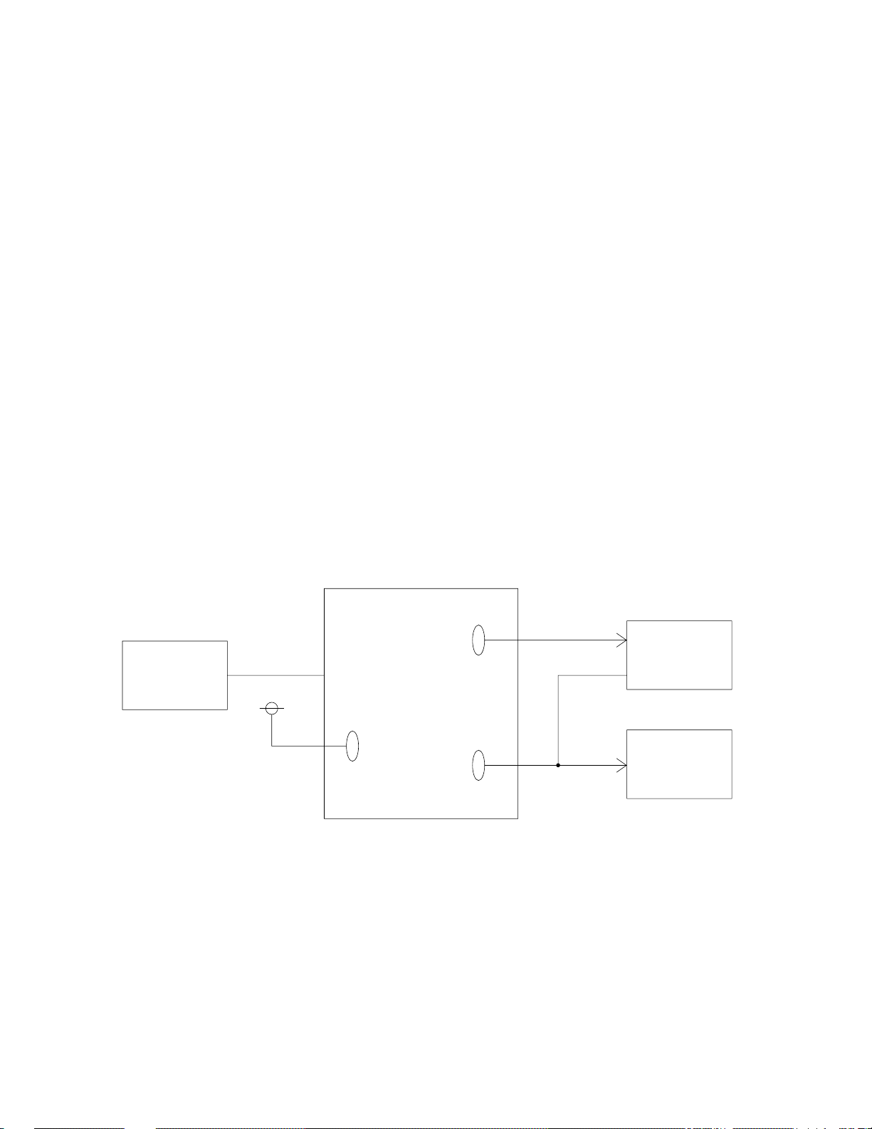
WIRING AND BLOCK DIAGRAM
Photo INT
Auto Iris Lens
Solenoid
CB-PCB
ICX098AK
15V
CCD
15V
-5.5V
Vdrv
CXD1267AN
3.5V
CXA2056Q
CDS+AGC
CXD2310R
ADC
3.5V
BR9040F
EEROM
T.G
3.3V
CXD2452R
20-pin
23-pin
8-pin
KEY-PCB
DA-PCB
60-pin
3.3V
YUV
Processor
CXD3120R
3.3V
3.0V
Switching
RS5C316A
RTC
UPD6466
OSD
MB91181
Detection
Switch
3.3V
MACO
3.2V
INTR
CFDET
Signal
Generator
Video
RS232C
EDO_
DRAM
Flash
Memory
3.3V
3.3V
3.3V
15.0V
-5.5V
5.0V
Battery Voltage
Voltage Controller
5V
VIDEO
RS232C
3.3V
CF
AC Adaptor
6.0V
10-pin
3.0V
4.5V
18.0V
12.0V
-10.5V
Transformer
5-pin
Battery voltage
GND
Battery voltage
GND
7-pin
Strobe Ass'y
Comparator
Photo
Sensor
Xenon Lamp
Battery
Voltage
Voltage Controller
Detection Sw.
(RSTW)
FUNC
button
LED
Chroma
IR3Y18A
Display Controller
CM7013L2
4.5V
3V
26-pin
BL
LCD module
High Voltage
Generator
5-pin
CA-PCB
Motor Driver
IRISA/IRISB
Battery Voltage
L-PCB
3.3V
7-pin
3.3V
— 2 —
Page 5
2 APO from Pin 202
of IC500
FU152 R590
C525
POWER SUPPLY CIRCUIT OPERATION
VCC1-1
3
1
2
Q580
IC584
1
OUT
VDD
GND
NC
NC
2
3
+
VCC1-1
5
4
Q582
VCC1-1
VCC1-1
IC586
5
VCC
1
4
2
3
GND
2
1
3
R585
IC582
1
2
7
6 Voltage detection signal
1 PON from
Key PCB
1
2
CN504
VCC3-1
PON
KEY0
KEY1
KEY2
SHTTER
GND
GND
Signal
PON
APO
2
Q588
3
C592
IC582
8
VCC
3
GND
IC588
R595
6
5
4
C590
R592
R593
1
2
3
4
VCC3-1
VCC1-1
1
R594
5
6
7
8
5 Power ON to Pin 1 of Q155
Operation
Power on/off signal (pulse) from Key PCB
Auto power off signal (pulse) from pin 202 of IC500
876
5
PR
CLR
VCC
CKDQ
123
4
VCC1-1
3
2
Q
GND
R579
Q583
3 POB to Pin193
of IC500
1
4 FACT from
Pin 195 of IC500
3
POB
Power on/off recognition signal to pin 193 of IC500
ON: H (VCC3) OFF: L (GND)
4
FACT
Forced power on signal from pin 195 of IC500
Forced ON: H (VCC3) OFF: L (GND)
ex. While writing to flash memory
5
Power On
Power on/off signal to pin 1 of Q155
ON: H (VCC1) OFF: L (GND)
6
Voltage
detection
Normal: H
Low voltage: L
— 3 —
Page 6
ADJUSTMENT
1. Unit Adjustment
Contents of the adjustment
(1) Color parameters loading
(2) Scratch compensation
(3) Flash adjustment
(4) Flash function check
(5) Current consumption check
(6) Clock reset
(7) Other test modes
Necessary equipments
(1) IBM PC/AT compatible computer
(2) Computer link cable
(3) Digital oscilloscope
(4) Stabilized power supply
(5) Ammeter
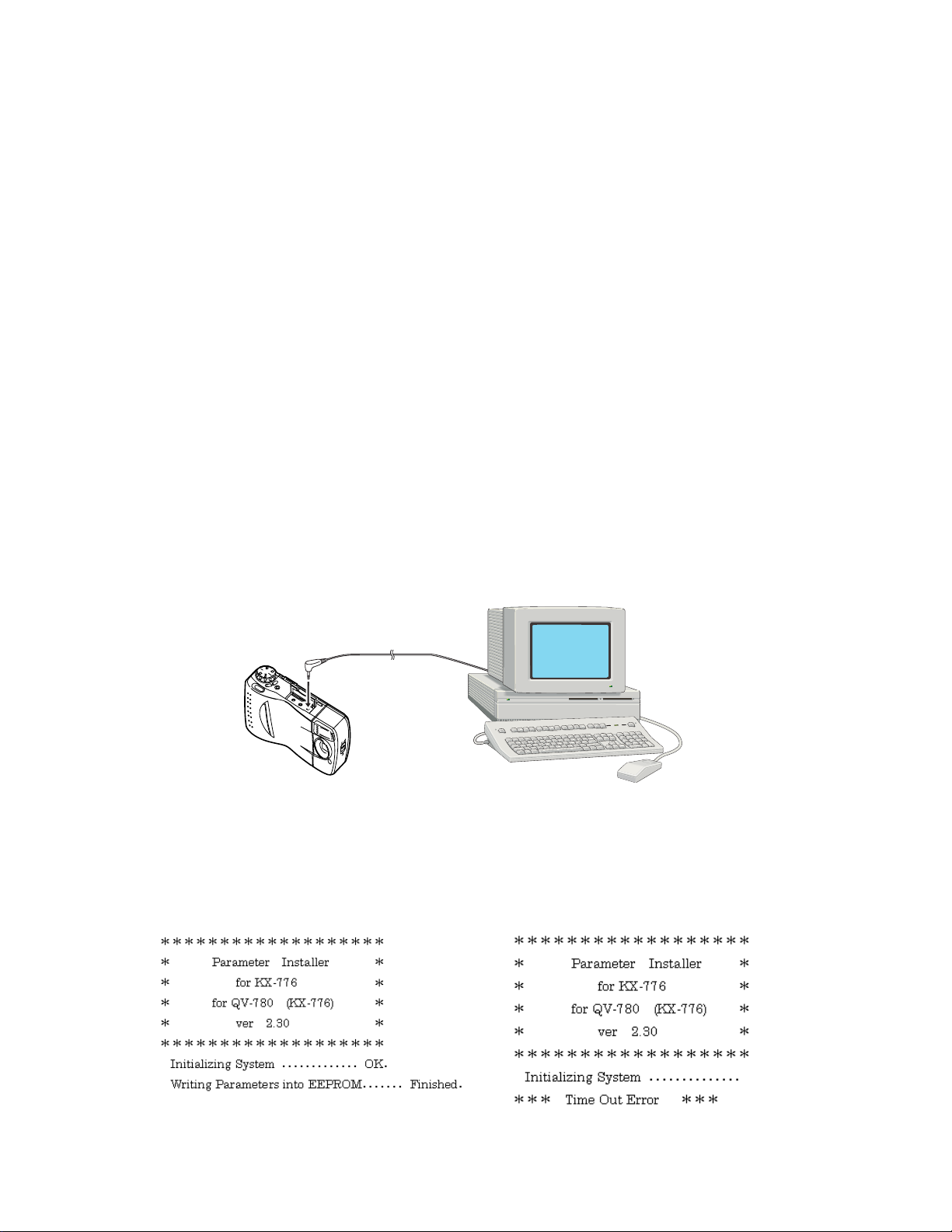
1-1. Color parameters loading
Perform the following procedures when you replaced Camera Unit.
(1) Set the QV-780 in “PLAY” mode.
(2) Connect the camera and a computer with a link cable.
To RS-232C
connector
Digital terminal
(3) Execute the following program on MS-DOS system.
PON776.EXE (for COM port 1)
(4) Loading is done successfully when computer monitor shows a message stating that loading is
completed.
When the loading is completed normally
.
When the loading is failed (example)
Note: After the loading, also perform the following Scratch compensation and Flash adjustment.
— 4 —
Page 7
1-2. Scratch compensation
1 meter
Gray paper
“Scratch” is a black dot which appears dimly on a white screen. Three scratches are allowable on
350,000 pxels screen. Perform this adjustment after loading color parameters.
(1) Set the QV-780 in “REC” mode.
(2) Set the dial on “ ” (PANORAMA MODE).
(3) While pressing down the SHUTTER and DEL buttons, turn the power on.
LCD screen indicates “TEST MODE”.
(4) While TEST MODE is indicated on the LCD, select the dial on .
Press “MENU” and “ ” buttons simultaneously.
LCD indicates;
CLOCK RESET
STROBE ADJUST
DEFECT CORRECT
BATTERY CHECK
(5) Cover QV-780 lens so that the light does not go in the
camera.
(6) Using “+” or “–” buttons, select “DEFECT CORRECT” and
press the SHUTTER button to execute the program.
(7) Make sure that the small red square mark on LCD turns in
blue.
(8) Turn the POWER switch off.
As the compensation data is written in the EEPROM by the
POWER switch operation, do not forget to turn it off using
the switch.
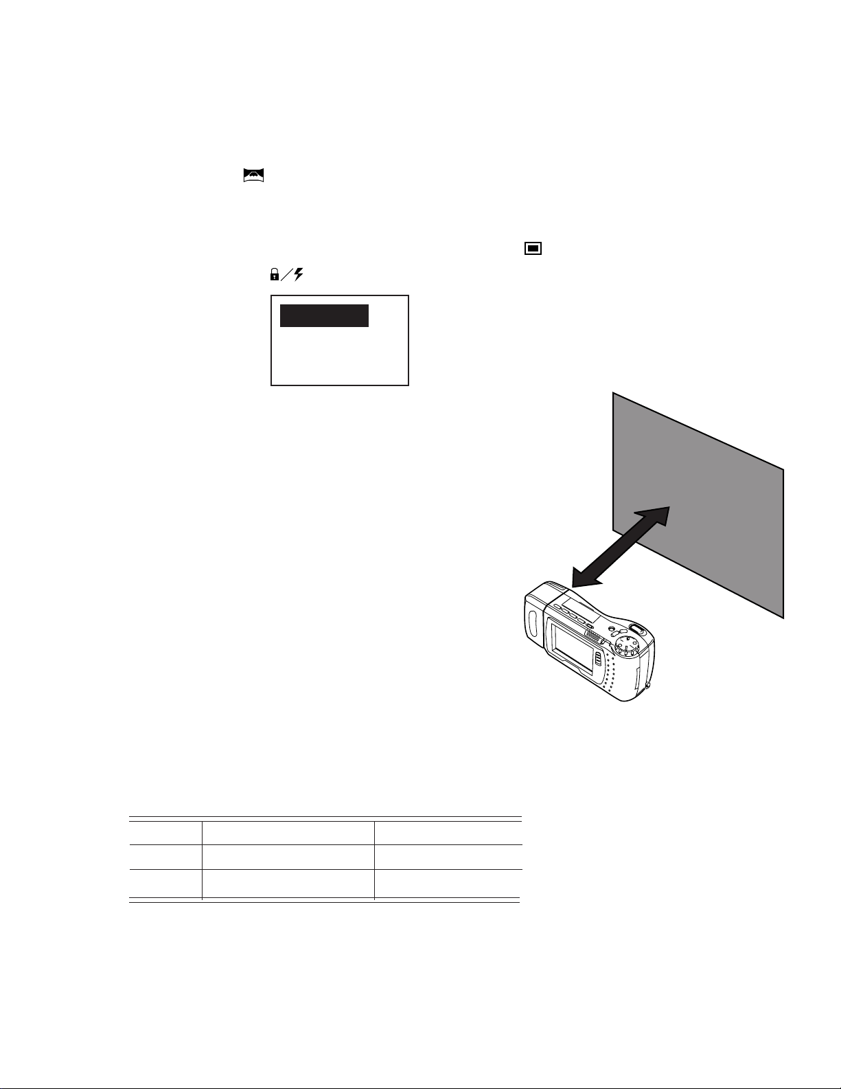
1-3.Flash adjustment
Perform this adjustment when you replaced the flash unit or
after color parameter loading.
Preparation and condition;
• Adjustments previously described should be completed.
• Distance between flash cover and gray paper should be one
meter.
• The adjustment must be done in a dark room.
• Use following gray paper for the testing.
Notes: •Use lighter color surface of the paper.
• Gray paper should be larger than the shooting area.
Code No. Name Specification
1904 5411 Superior Seamless Paper No. 22 (1.75 x 2.7 m)
1904 5412 Superior Seamless Paper No. 22 (2.72 x 11 m)
Though these papers are available from Casio, large camera stores handle them.
— 5 —
Page 8
(1) Set the QV-780 in “REC” mode.
(2) Execute the test program.
• Set the dial on “ ” (PANORAMA MODE).
• While holding down the “SHUTTER” and “DELETE” buttons, turn the POWER on.
• While TEST MODE is indicated on the LCD, select the dial on .
Press “MENU” and “ ” buttons simultaneously.
LCD indicates;
CLOCK RESET
STROBE ADJUST
DEFECT CORRECT
BATTERY CHECK
(4) Use “+” or “–” buttons to select “STROBE ADJUST” and press the SHUTTER button.
(3) Shot a picture of the test paper.
(Flash indicator should be red before shooting.)
(5) Make sure that the flash icon turns from red to blue.
(If it does not turn into blue, IC531 might be faulty.)
(6) Turn the POWER switch off.
As the adjustment data is written in the EEPROM by the POWER switch operation, do not forget
to turn it off using the switch.
1-4.Flash check
This test is to make sure that the flash circuit is not affected by undesirable electric noise. Perform
this test whenever you changed wirings of the camera unit.
Conditions;
• Perform after the flash adjustment
• Use “ ” button to select Flash On.
• Apply 6.0 ± 0.1 [V] voltage on DC IN jack.
(1) Set the QV-780 in “REC” mode and press the shutter.
(2) Using a digital oscilloscope, monitor flash trigger pulse.
Voltage
A
Ammeter
Put oscilloscope probe
on Camera unit.
Regulator
DC6.0±0.1V
Digital oscilloscope
TIME: 1.0¨ µsec/div
VOLTS: 1V/div (AC)
Correct waveform
OK if this peak is shown
TIME: 1µsec/div
VOLTS: 1V/difv
NG waveform
2nd positive peak is not
shown.
— 6 —
TIME: 1µsec/div
VOLTS: 1V/difv
Page 9
(3) Set the QV-780 on “PLAY” mode and make sure that the picture taken is not too dark or too light.
(4) After the shot, flash is charged automatically. Observing the ammeter, make sure that the charging
current is less than 1.2 [A].
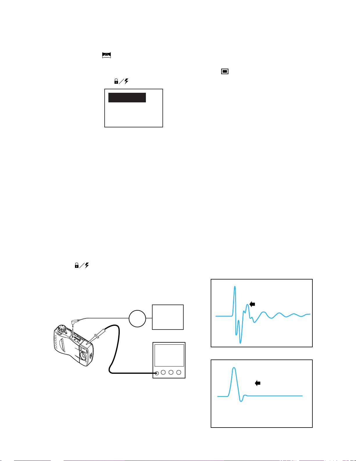
If the following pictures are taken, it may be caused by faulty wirings.
Shrinken
To solve this problem, install the wires as shown below.
Strobe
white wire in front. The
other four wires in the
back.
Lens
Removable
for correction
*Warning: Discharge
capacitor before operat-
Note: Red wire and
ing in accordance with
DISASSEMBLY proce-
Red wire
dure of page 19. There
is a risk of electric
shock.
1-5.Current consumption
Soldering
White wire
(1) Set the QV-780 in “REC” mode. After the flash circuit is fully charged, make sure that the current
consumption is less than 550 [mA] (for example, at PLAY mode, current consumption is 380 [mA]
when the flash is fully charged.
(2) Reduce the power supply voltage to 3.8 [V] and make sure that the low battery warning indicator
is shown.
1-6.Clock reset
Perform the following procedures when you replaced PCB K772-DA.
(1) Set the QV-780 in “REC” mode.
(2) Execute the test program.
• Set the dial on “ ” (PANORAMA MODE).
• While holding down the “SHUTTER” and “DELETE” buttons, turn the POWER on.
• While TEST MODE is indicated on the LCD, select the dial on .
Press “MENU” and “ ” buttons simultaneously.
LCD indicates;
CLOCK RESET
STROBE ADJUST
DEFECT CORRECT
BATTERY CHECK
— 7 —
Page 10
(3) Using “+” or “–” buttons, select “CLOCK RESET” and press the SHUTTER button to execute the
program.
1-7.Other test modes
(1) Set the QV-780 in “REC” mode.
(2) Execute the test program.
• While holding down the “SHUTTER” and “DELETE” buttons, turn the POWER on.
• While TEST MODE is indicated on the LCD, press “MENU” and “ ” buttons simultaneously.
LCD indicates;
BLACK
COLOR BAR
APO OFF
(3) Using [ + ] or [ – ] buttons, select a test mode then press “SHUTTER”.
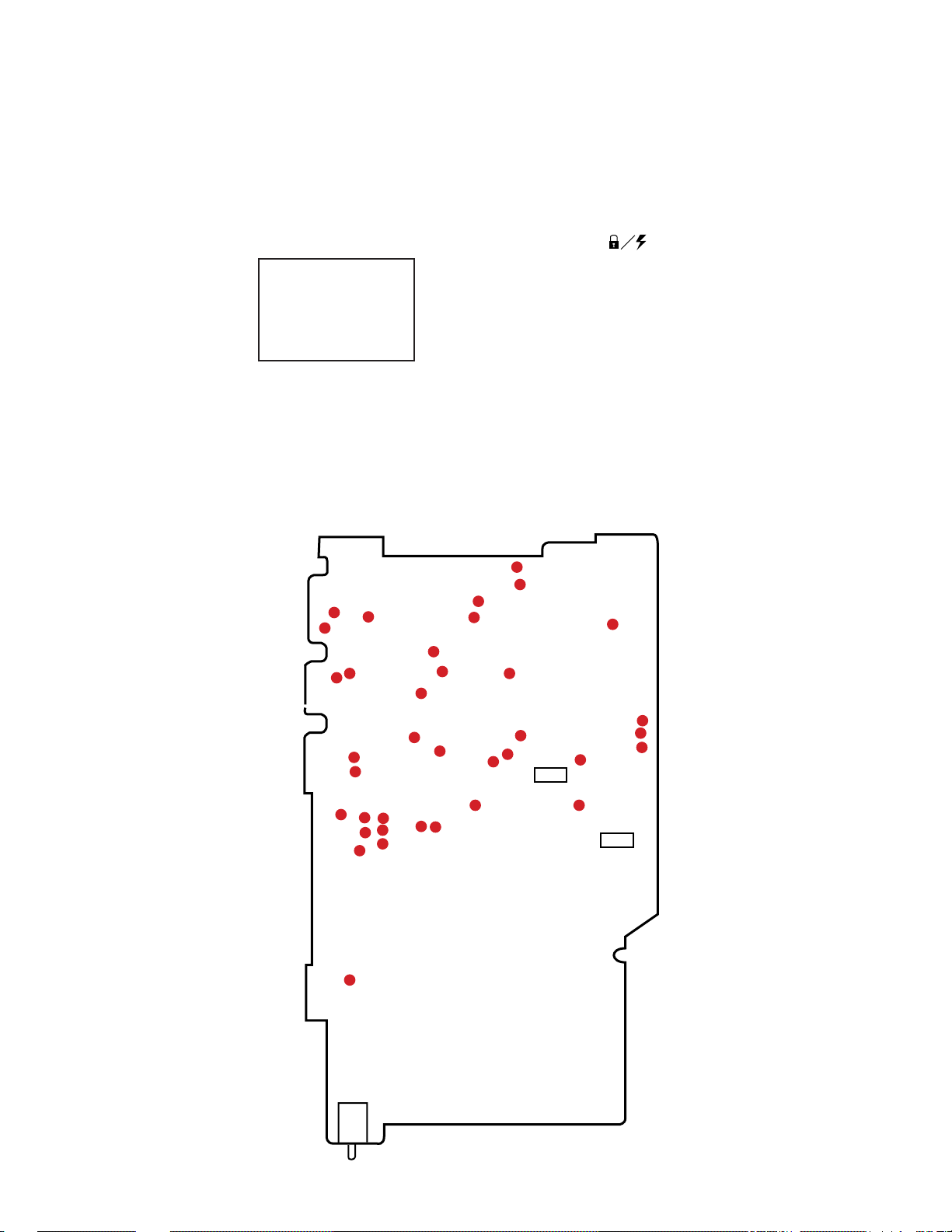
2. PCB K772-DA Adjustment
Contents of the adjustment
(1) VCC1, VCC3 checks
(2) VCC7, VEE3 adjustments
(3) Clock oscillation frequency check
Checkpoints
CP562
CP561
CP567
CP151
CP573
CP566
CP596 CP150
CP592
CP154
CP153
CP560
CP595
CP594
CP593
CP540
CP155
CP160
CP165
CP167
CP161
CP541
CP166
CP182
CP175
CP175
CP168
CP164
CP184
CP183
CP570
CP520
VR651
CP170
CP171
CP578
CP572
CP571
CP529
VR650
SW502
— 8 —
Page 11

2-1. VCC1, VCC3 voltage check
Apply 5.0 ± 0.05 [V] on check point CP150. (For normal check you can use an AC adaptor however,
when the camera is faulty, apply the above mentioned voltage.)
(1) At Power on;
VCC1 (CP164) ................. 3.2 ± 0.16 [V]
VCC5-1 (CP165) .............. 5.25 ~4.75 [V]
VCC5-2 (CP166) .............. 5.25~4.75 [V]
VCC3-1 (CP167) .............. 3.3 ± 0.17 [V]
VCC3-3 (CP168) .............. 3.3 ± 0.17 [V]
VCC3-4 (CP169) .............. 3.3 ± 0.17 [V]
(2) At Power off;
VCC3-1 (CP164) .............. 0 [V]
2-2.VCC7, VEE3 adjustment
Apply 5.0 ± 0.05 [V] on check point CP150. (For normal check you can use an AC adaptor however,
when the camera is faulty, apply the above mentioned voltage.)
(1) Adjust VR650 so that VCC7 (CP170) is 15.0 ± 0.45 [V].
(2) Adjust VR651 so that VEE3 (CP171) is -5.5 ± 0.2 [V].
2-3.Clock oscillation check
• Apply 3.2 ± 0.1 [V] on lithium battery terminal (CP578).
• Turn power off.
• Room temperature should be 25 ± 10 °C.
(1) Use quartz timer or frequency counter to measure clock frequency.
• Quartz timer; within ± 62 ppm
• Frequency counter (check point TC500 signal pad); 32.767 ± 0.002 [KHz}
(2) Current consumption; less than 1 [µA]
— 9 —
Page 12
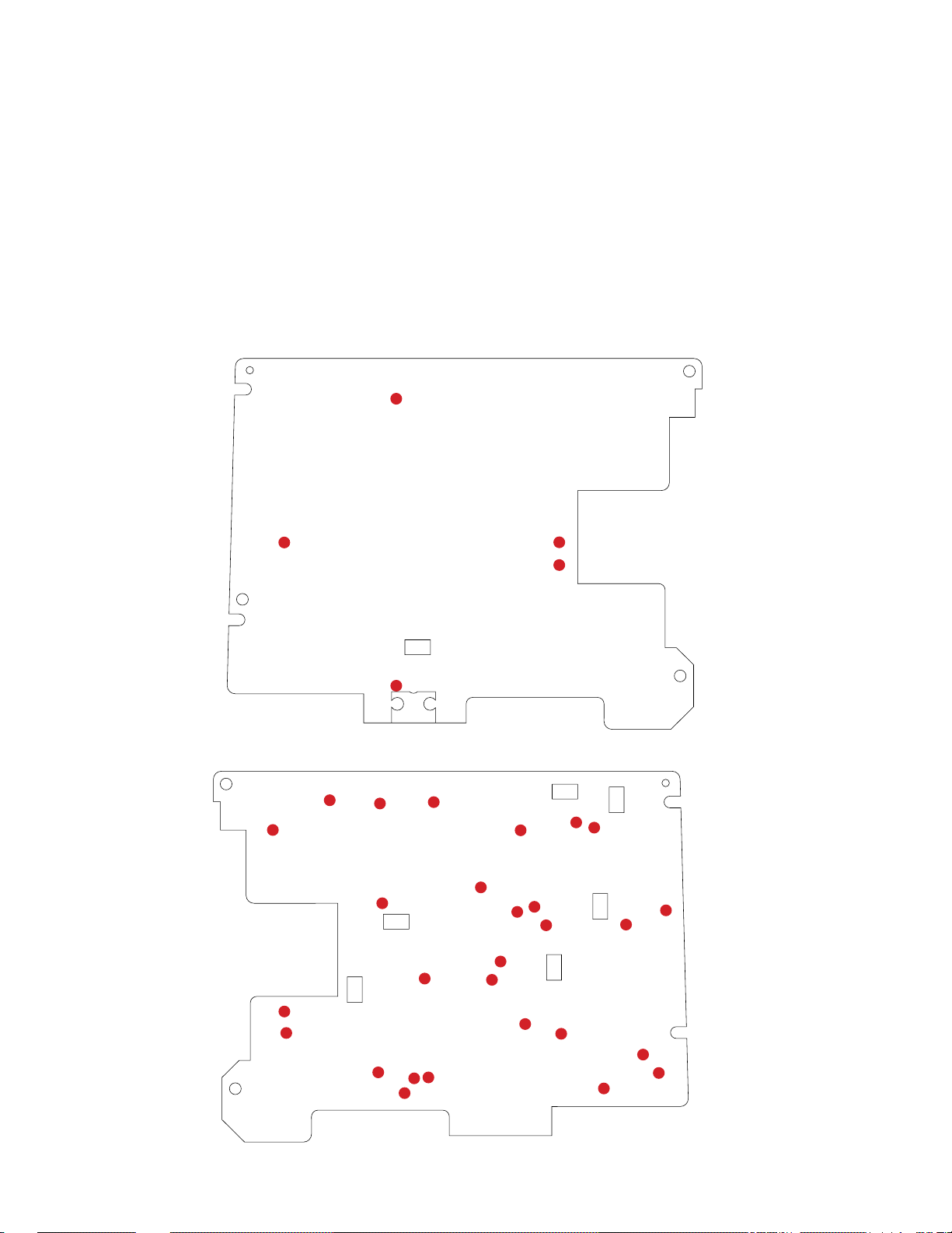
3. PCB K772-L Adjustment
Contents of the adjustment
(1) VCC1 adjustment and VCC2, VCC6, VEE2, VCC0 voltage check
(2) VCO free run frequency adjustment
(3) Backlight drive voltage adjustment
(4) VCOM AC adjustment and VCOM DC coarse adjustment
(5) Brightness voltage setting and contrast adjustment
(6) BCC adjustment
(7) Color adjustment
(8) VCOM DC fine adjustment
Check points
CP317
CP700
CP149
CP900
CP114 CP110
CP901
CP100
VR900
CP146
CP140
CP350
CP111
VR100
CP147
VR350
VR302
CP101
CP145
CP112
CP322
CP120
CP902
VR303
CP300
CP344
CP324
CP320 CP711
CP113
CP733
CP115
CP725
CP308
VR710
CP351
VR301
VR300
CP337
CP142
CP141
— 10 —
Page 13
3-1.VCC1 adjustment and VCC2, VCC6, VEE2, VCC0 voltage check
Apply 5.0 ± 0.05 [V] on check point CP101. (For normal check you can use an AC adaptor however,
when the camera is faulty, apply the above mentioned voltage.)
(1) Adjust VR100 so that VCC1 is 4.50 ± 0.02 [V]
(2) Check the following voltages.
VCC2 ...................... 11.5 ~ 12.5 [V]
VCC6 ...................... 17.5 ~ 19.5 [V]
VEE2....................... -9.5 ~ -11.5 [V]
VCC0 ...................... 2.8 ~ 3.2 [V]
(3) Turn the power off and make sure that all the voltages are 0 [V].
3-2.VCO free run frequency adjustment
• Show color bar in test mode.
• Apply 5.0 ± 0.05 [V] on check point CP101. (For normal check, AC adaptor can be used, however,
when the camera is faulty, apply the above mentioned voltage.)
• Connect check points CP725 (SYF) and CP115 (VCC0).
(1) Monitoring CP733 (HDB) with a frequency counter, adjust VR710 so that the frequency is 15.625 ±
0.1 [KHz].
(2) Disconnect CP725 and CP115 and make sure that signals of CP337 (CSY) and CP733 (HDB) are
synchronized.
Power
Supply
VCC0
PCB K772A-L
SYF
(CP725)
QV-780
CSY
(CP337)
HDB
(CP733)
CSY
Oscilloscope
HDB
Frequency
Counter
— 11 —
Page 14

3-3.Backlight drive voltage adjustment
Power
Supply
Oscilloscope
2.5±0.2 [V]
0 [V]
PCB K772A-L
QV-780
VCOM
(CP351)
Apply 5.0 ± 0.05 [V] on check point CP101. (For normal check, AC adaptor can be used, however,
when the camera is faulty, apply the above mentioned voltage.)
(1) Adjust VR900 so that CP901 (VBL) is 11.5 ± 0.1 [V].
Also make sure that the current consumption is not abnormally large.
3-4.VCOM AC adjustment and VCOM DC coarse adjustment
• Show color bar in test mode.
• Apply 5.0 ± 0.05 [V] on check point CP101. (For normal check, AC adaptor can be used, however,
when the camera is faulty, apply the above mentioned voltage.)
(1) Make sure that the oscillation level of VCOM output (CP351) is 6.0 ± 0.3 [V].
(2) Adjust VR350 so that the low level potential is 2.5 ± 0.2 [V].
— 12 —
Page 15

3-5.Brightness voltage setting and contrast adjustment
Power
Supply
Oscilloscope
22K
2.9±0.1
5.0±0.1V
Killer terminal
(CP308)
VB terminal
(CP324)
(L-PCB)
QV-780
VCC1
• Show color bar in test mode.
• Apply 5.0 ± 0.05 [V] on check point CP101. (For normal check, AC adaptor can be used, however,
when the camera is faulty, apply the above mentioned voltage.)
(1) Via 22 kohm resistor apply VCC1 (CP113) voltage on killer terminal (CP308).
(2) Adjust BRIGHT VR (VR302) so that pedestal voltage of VB (CP324) signal is 5.0 ± 0.1 [V].
(3) Connect oscilloscope’s trigger terminal to FRP (CP711) for external trigger.
(4) Adjust VR303 so that potential between VB (CP324) signal’s pedestal and white peak is 2.9 ± 0.1 [V].
• Make sure that the waveforms are not distorted.
• After the adjustment, disconnect the voltage supply of the killer terminal.
• Do not turn BRIGHT VR until TINT and COLOR adjustments are completed.
— 13 —
Page 16

3-6.BCC adjustment
Power
Supply
Adjust to same level
Oscilloscope
L-PCB
VB terminal
(CP324)
• Perform this procedure with color adjustment
• Show color bar in test mode.
• Power supply voltage VCL 0 (CP101) = 5.0 ± 0.05 V.(For normal check, AC adaptor can be used,
however, when the camera is faulty, apply the above mentioned voltage.)
• Adjust L300 so that four pulses of VB waveforms (CP324) almost have no amplitude.
(1) Perform this procedure after contrast adjustment.
(2) Set the pedestal voltage of VB to 5.0 ± 0.1 Vp-p by adjusting BRIGHT VR (VR302).
(3) Use FRP (CP711) for trigger.
(4) If waveform changes by adjusting color perform Step (2).
— 14 —
Page 17

3-7.Color adjustment
Power
Supply
4.1 ± 0.1 [V]
Oscilloscope
L-PCB
VB terminal
(CP324)
1
234
4
2
1
3
• Perform this procedure together with BCC adjustment.
• Show color bar in test mode.
• Power supply voltage VCL 0 (CP101) = 5.0 ± 0.05 V(For normal check, AC adaptor can be used,
however, when the camera is faulty, apply the above mentioned voltage.)
• Adjust VR300 so that the first 1 the second 2 pulse of VB waveform (CP324) becomes 4.1 ± 0.1 V.
(1) Perform this procedure after contrast adjustment.
(2) Set the pedestal voltage of VB to 5.0 ± 0.1 Vp-p by adjusting BRIGHT VR (VR302).
(3) Use FRP (CP711) for trigger.
(4) If waveform changes by adjusting BCC perform step (2).
(5) Make sure 3 and 4 have almost the same value.
3-8.VCOM DC adjustment
• Perform this adjustment when you replace the display module.
• No signal input
• BRIGHT VR: Maximum
• Apply 6.0 ± 0.1 [V] (DC in). (For normal check, AC adaptor can be used, however, when the camera
is faulty, apply the above mentioned voltage.)
(1) Adjustment VR350 if the display is flikered, dimmed or discolored with watching the LCD screen.
(2) If the adjustment cannot be done well, passing photosensor amp output signal through 60 Hz
band-pass filter, adjust VR350 to minimize the ripple of 60 Hz signal as shown below.
Photo diode
S1153
Photosensor amp.
C2719
QV-780
B.P.F.
Oscilloscope
Power supply
Adjust VR350
to minimize the
ripple.
— 15 —
Page 18

DISASSEMBLY
The following explains the disassembly procedure of QV-780. Numbers in the procedures correspond to the
part numbers on the exploded view.
Assembly can be done by the reverse order.
1. Remove the CompactFlash card by pushing the release lever.
2. Remove two screws j from the bottom of the camera.
3. Unscrew two screws f from the lens side of the case.
Note:Turn the lens as screws f are hidden by the Camera unit 1.
4. Remove three screws h and one screw i from the CompactFlash card compartment.
Note: Screw i is longer than the others. Do not misplace it when you assemble the camera.
i
— 16 —
Page 19

5. Prying the case R, remove the battery cover and CompactFlash card cover.
6. Unhook the upper part of Case/Upper R and open the case.
Unhook here
7. Desolder a lead wire from PCB Ass’y/Linear a and disconnect FPC from the connector CN514 on PCB
Ass’y/Digital. Separate Case/Upper R and Case/Lower E.
8. Remove two screws g and disconnect two connectors from PCB A’ssy/Digital then separate Camera
unit 1.
9. Remove two screws f from PCB Ass’y/Digital 2 and detach FPC from connector CN504.
— 17 —
Page 20

10.Lift up the buttom of the battery compartment and remove Holder/Battery 3 and PCB Ass’y/Digital.
Note: Before you remove Holder/Battery 3, be
sure that CompactFlash card release lever
is in upright position.
11.Take Knob/Selector 6 and PCB Ass’y/Key 5 off the case.
Note: Knob/Selector 6 can be removed by unscrewing two screws f from the bottom of the knob.
12.Peel Grip K then remove one screw h from Panel/Rear J.
Unclip the E-ring from Pin J.
Note: Peel Panel/Rear carefully off Case/Lower E as it is attached with adhesive tapes.
Removing LCD Unit
13.Remove four screws l from PCB Ass’y/Linear a.
— 18 —
Page 21

14.Lift up the stopper tab of connector CN700 and disconnect FPC cable. Also disconnect connector CN920.
15.Remove the BRIGHT knob T and take PCB Ass’y/Linear off the case.
Note: Be careful not to bend or break the LED on the other side of the PCB.
16.Remove Three screws l from BL ass’y _ then remove the BL ass’y.
Note: Do not touch BL ass’y with naked hand.
17.Remove Spacer ] and Display Ass’y [.
Note: Do not touch Display Ass’y with naked hand.
Camera Unit
18.Remove three screws h and m.
— 19 —
Page 22

19.Peel off the caution label.
Caution: Since high-voltage is applied on the circuits on Camera Unit, there is a risk of electric shock.
Before proceeding to the following steps, discharge 70 µF, 300 V capacitor with a 1.5 kohm,5 W cement
resistor.
1.5 kohm/5W
resistor
20.Remove two screws and disconnect two wires red and white.
21.Remove Strobe unit 1-3 .
22.Remove two screws from the gear.
Peel off the adhesive tape wrapped around the case shaft.
— 20 —
Page 23

23.Twisting the FPC cable and pulling out the connector throught the hole on the gear, pull the gear out.
24.Remove one screw l.
25.Disconnect FPC cables from the connectors CN200, CN201, and CN501 then remove CCD unit 1-2 .
— 21 —
Page 24

PCB K772-L
PRINTED CIRCUIT BOARDS
Top view
— 22 —
Page 25

PCB K772-L
Bottom view
— 23 —
Page 26

PCB K772-DA
Top view
— 24 —
Page 27

PCB K772-DA
Bottom view
— 25 —
Page 28

TROUBLESHOOTING
Problem Cause Solution
Display shows “DIAL” and
buttons do not work.
Display shows
CF
CF ERROR
FORMAT ➝ MENU
1. Dial key is placed in an odd place.
2. SW502 of DA assembly keeps
turning on.
1. Erroneous CF card data.
2. CF card hard drive error.
(Unable to execute Scan Disk or
format)
3. Broken circuit or broken connector on CF card of DA assembly
1. Turn the Dial key until it makes a
click sound, when there is no click
sound, click spring of key assembly may be broken or distorted.
2. Replace SW502.
1. Read P109 of Instruction Manual.
CF card can be handled the same
way as hard drive.
Try the actions noted below.
1) Set CF card to the PC using PC
card adapter.
2) Save the correct file in memory
file.
3) Execute “Scan Disk” on CF card
and correct the data of format.
4) Save the correct data than copy it
onto CF card.
2. Consult to technical support.
3. Replace connector of DA assembly.
Display shows
SYSTEM ERROR
CALL TECH
SUPPORT
Display shows
CF
NO CARD
Power will not turn on.
No display.
Flash not rechargeable/
will not flash
1. Bad connection between DA assembly and camera unit.
2. Erroneous EEPROM.
(exclude CF card)
1. No CF card.
2. Broken circuit or broken connector on CF card of DA assembly.
1. Memory card cover is open, or
SW502 is broken.
2. FU150 is broken.
3. Flat cable connecting DA assembly and L assembly is loose or
broken.
4. Flat cable connecting DA assembly and key assembly is loose or
broken.
1. LCD connector of BL connector is
open.
2. IC701 is broken or bad soldering.
1. IC531 is broken or bad soldering.
1. Reconnect the connector.
2. Execute DA assembly check program. If NG, replace.
1. Insert CF card
2. Replace connector or DA assembly.
1. Close memory card cover, or replace SW502.
2. Replace FU150.
3. Reinsert the flat cable or replace
the flat cable.
4. Reinsert the flat cable or replace
the flat cable.
1. Insert connectors.
If broken replace them.
2. Resolder or replace IC.
1. Refer to “Strobe adjustment”
— 26 —
Page 29

Problem Cause Solution
Display failure when
using flash
Cannot switch
between REC and
PLAY
Incorrect time.
Battery consumption is early.
1. Noise when strobe flashes.
1. Slide switch is broken or incorrectly
assembled.
1. Bad connection between DA assembly and camera unit.
2. Incorrect time data.
3. Lithium battery is dead.
4. Bad DA assembly.
1. Refer to P8, 29, 30, 31, and 112 of
Instruction Manual.
2. Current consumption is high.
3. Kept battery in the camera for a long
periods of time.
1. Refer to “Strobe operation check”
1. Replace switch or reassemble.
1. Reconnect connector.
2. Refer to “Reset time”. Set time.
3. Replace lithium battery.
4. Refer to “Clock oscillator frequency
check”
1. Battery life differs depending on manufacturers, types, temperatures, and
storage periods. The figures in the
Instruction Manual are approximations and are not guaranteed.
2. Refer to “Current consumption check”
3. Take the batteries out when not using
the camera for a long periods of time.
(Even when the power is turned off
minute currency (0.xx mA) is consumed.)
When switching
from PLAY to REC
LCD display turns
blue and keys do
not work. (Cannot
turn power off.)
Display failure.
(Flash not in use)
1. Bad connection between DA assembly and camera unit, or camera unit is
broken.
1. Bad connection between DS assembly and camera unit.
2. EEPROM data error.
3. Camera unit is broken.
1. Reconnect the connector, or replace
L case assy or CL unit or CAM case
unit.
1. Reconnect connectors.
2. Execute “Loading color parameters”
3. Replace L case assy or CL unit or
CAM case unit.
— 27 —
Page 30

MAIN BODY
46
EXPLODED VIEW
1
47
24
23
46
59
47
44
10
27
29
2
50
50
30
31
3
46
3-1
2-1
45
8
9
3-3
7
5-1
3-2
5
51
39
4
6
36
37
26
38
25
28
40
32
48
33
34
35
49
17
18
19
16
20
48
11
55
21
12
13
14
15
48
— 28 —
52
22
43
46
40-1
52
42
52
41
52
41-1
Page 31

CAMERA UNIT
1-1
1-2
48
1-10
1-9
53
54
1-7
1-3
52
1-4
1-5
1-11
1-6
1-8
— 29 —
Page 32

PARTS LIST
LINEAR PCB ASS'Y
Item Code No. Parts Name Specification Applicable Q R
Diodes
D110 7101 1194 DIODE MA111-(TX) Common 1 C
D111 2390 1379 DIODE/SCHOTTKY MA729-(TX) Common 1 C
D112 2390 1379 DIODE/SCHOTTKY MA729-(TX) Common 1 C
D113 7101 1194 DIODE MA111-(TX) Common 1 C
D700 7101 1194 DIODE MA111-(TX) Common 1 C
D710 2390 1358 DIODE/VARICAP MA329-(TX) Common 1 C
D900 2390 1421 DIODE/SCHOTTKY MA738-(TX) Common 1 C
ICs
IC100 2114 3654 IC MB3800PNF-G-BND-EF Common 1 C
IC130 2105 4501 IC/MOS RN5RL30AA-TR Common 1 C
IC300 2114 5804 IC IR3Y18A Common 1 C
IC350 2114 5805 IC NJM3414AV-TE1 Common 1 C
IC700 2012 5744 LSI CM7013L2-T4N Common 1 C
IC701 2105 6397 IC TC74VHCT04AFT(EL) Common 1 C
IC900 2114 3654 IC MB3800PNF-G-BND-EF Common 1 C
IC920 7720 0700 IC TC7S02FU-TE85L Common 1 C
LED
D140 2370 1396 LED SLC-22DU3F Common 1 C
Transistors
Q100 2253 0308 TRANSISTOR 2SD1119-R(TX) Common 1 B
Q140 7911 0126 TRANSISTOR/DIGITAL DTC144EUAT106 Common 1 B
Q141 7911 0126 TRANSISTOR/DIGITAL DTC144EUAT106 Common 1 B
Q900 2253 0308 TRANSISTOR 2SD1119-R(TX) Common 1 B
Q901 7911 0126 TRANSISTOR/DIGITAL DTC144EUAT106 Common 1 B
Q950 2253 0700 TRANSISTOR 2SK1485-T1 Common 1 B
Switches
SW140 3412 2080 SWITCH SSSS712-ZA Common 1 C
SW141 3412 2002 SWITCH SPVC2-1-T Common 1 C
Converter and Transformaer
T100 3065 0711 CONVERTER/DC-DC 6CA-01 Common 1 B
T900 3012 1477 TRANSFORMER/INVERTER ETJ09K20AM Common 1 B
Variable resistor
VR302 2775 0644 RESISTOR/SEMI-FIXED H0614D-10KB Common 1 C
Diodes
D151 2390 2506 DIODE RB060L-40-TE25 Common 1 C
D155 2390 1379 DIODE/SCHOTTKY MA729-(TX) Common 1 C
D160 2390 2394 DIODE/SCHOTTKY U1FWJ44N-TE12L Common 1 C
D161 2390 1379 DIODE/SCHOTTKY MA729-(TX) Common 1 C
D170 2390 1379 DIODE/SCHOTTKY MA729-(TX) Common 1 C
D171 7101 1194 DIODE MA111-(TX) Common 1 C
D510 2390 1379 DIODE/SCHOTTKY MA729-(TX) Common 1 C
D513 2390 1379 DIODE/SCHOTTKY MA729-(TX) Common 1 C
D525 2259 2735 DIODE/SCHOTTKY HRW0202ATL Common 1 C
D660 7101 1194 DIODE MA111-(TX) Common 1 C
Fuses
FU150 3632 0630 FUSE KE10 Common 1 A
FU151 3632 0724 FUSE KE13 Common 1 A
FU152 3632 0709 FUSE KE16 Common 1 A
Notes: Q – Quantity used per unit
R – Rank
— 30 —
Page 33

DIGITAL PCB ASS'Y
Item Code No. Parts Name Specification Applicable Q R
ICs
IC150 2114 5806 IC TK11232BMCL Common 1 C
IC152 2105 3374 IC/CMOS RS5RM5045A-T1 Common 1 C
IC156 2105 6404 IC XC6375A311PR Common 1 C
IC400 2114 5808 LSI CXD3120R Common 1 C
IC500 2114 5809 LSI MB91181PMT-G Common 1 C
IC502 2114 5810 IC S-80930ALMP-DAT-T2 Common 1 C
IC503 2114 5810 IC S-80930ALMP-DAT-T2 Common 1 C
IC505 2012 6059 LSI MBM29LV400T-10-019 Common 1 C
IC507 2012 5747 LSI MB81V16165B50LPFTN Common 1 C
IC510 2105 5712 IC TC7S04FU(TE85L) Common 1 C
IC515 2105 6378 IC MM1228XFBE Common 1 C
IC529 7911 0105 OP-AMP TA75S01F(TE85L) Common 1 C
IC530 7911 0105 OP-AMP TA75S01F(TE85L) Common 1 C
IC531 2105 6361 IC/MOS XC61AC2402MR Common 1 C
IC540 2012 5950 LSI UPD6466GS-514-E1 Common 1 C
IC545 2105 6425 IC/MOS XC61AN3802MR Common 1 C
IC550 2105 6399 IC RS5C316A-E2 Common 1 C
IC580 2105 5516 IC/CMOS TC7W126FU-TE12L Common 1 C
IC582 6571 0037 IC/L-MOS TC7W00FU(TE12L) Common 1 C
IC584 2114 5817 IC S-80936ANMP-DD0-T2 Common 1 C
IC586 2105 3521 IC/CMOS TC7S08FU-TE85L Common 1 C
IC588 2105 5215 IC/CMOS TC7W74FU(TE12L) Common 1 C
IC651 2105 5999 IC XC6383F501MR Common 1 C
IC652 2114 5607 IC TK11830MTL Common 1 C
Jacks
JK150 3501 6755 JACK HEC3600-010120 Common 1 C
JK510 3501 6538 JACK HSJ1169-012010 Common 1 C
JK515 3501 5439 JACK HSJ1456-01-210 Common 1 C
Switch
SW502 3412 2002 SWITCH SPVC2-1-T Common 1 C
Transistors
Q155 2259 2715 TRANSISTOR/DIGITAL DTC144EETL Common 1 B
Q156 2259 2716 TRANSISTOR 2SC4617TLR Common 1 B
Q158 2114 5807 FET SI3441DV-T1 Common 1 B
Q159 7101 5791 TRANSISTOR/DIGITAL DTA144EETL Common 1 B
Q169 2259 2716 TRANSISTOR 2SC4617TLR Common 1 B
Q507 2259 2715 TRANSISTOR/DIGITAL DTC144EETL Common 1 B
Q508 2259 2731 TRANSISTOR/DIGITAL DTA114EE-TL Common 1 B
Q510 2259 2731 TRANSISTOR/DIGITAL DTA114EE-TL Common 1 B
Q511 2259 2715 TRANSISTOR/DIGITAL DTC144EETL Common 1 B
Notes: Q – Quantity used per unit
R – Rank
— 31 —
Page 34

Item Code No. Parts Name Specification Applicable Q R
Q515 2254 0448 FET 2SK1580-T1 Common 1 B
Q520 2259 2716 TRANSISTOR 2SC4617TLR Common 1 B
Q521 2250 1579 TRANSISTOR 2SA1774TLR Common 1 B
Q522 2259 2716 TRANSISTOR 2SC4617TLR Common 1 B
Q539 2259 2715 TRANSISTOR/DIGITAL DTC144EETL Common 1 B
Q540 2250 1579 TRANSISTOR 2SA1774TLR Common 1 B
Q541 2251 0926 TRANSISTOR 2SB1412TLQ Common 1 B
Q543 2259 2716 TRANSISTOR 2SC4617TLR Common 1 B
Q580 2259 2715 TRANSISTOR/DIGITAL DTC144EETL Common 1 B
Q582 7101 5791 TRANSISTOR/DIGITAL DTA144EETL Common 1 B
Q583 2259 2715 TRANSISTOR/DIGITAL DTC144EETL Common 1 B
Q585 2259 2715 TRANSISTOR/DIGITAL DTC144EETL Common 1 B
Q588 2250 1579 TRANSISTOR 2SA1774TLR Common 1 B
Q650 2253 0308 TRANSISTOR 2SD1119-R(TX) Common 1 B
Q651 2259 2715 TRANSISTOR/DIGITAL DTC144EETL Common 1 B
Q652 2251 0882 TRANSISTOR 2SB1073-(TX) Common 1 B
Q653 2259 2715 TRANSISTOR/DIGITAL DTC144EETL Common 1 B
Q660 2250 1579 TRANSISTOR 2SA1774TLR Common 1 B
KEY PCB ASS'Y
Item Code No. Parts Name Specification Applicable Q R
IC
IC600 2105 6398 IC LB1846M-TE-L Common 1 B
Switches
SW801 2254 0555 SWITCH ESE22MH4 Common 1 B
SW802 3412 2068 SWITCH EVQPQHB55 Common 1 C
SW803 3412 2068 SWITCH EVQPQHB55 Common 1 C
SW804 3412 2068 SWITCH EVQPQHB55 Common 1 C
SW805 3412 2068 SWITCH EVQPQHB55 Common 1 C
SW806 3412 2068 SWITCH EVQPQHB55 Common 1 C
SW807 3412 2068 SWITCH EVQPQHB55 Common 1 C
SW808 3412 2068 SWITCH EVQPQHB55 Common 1 C
SW809 3412 2068 SWITCH EVQPQHB55 Common 1 C
SW810 3412 2068 SWITCH EVQPQHB55 Common 1 C
SW811 3412 2081 SWITCH SPVC2-1-B Common 1 C
Variabl Resistor
SW800 2765 2193 VOLUME RK10J11F0001A Common 1 C
Notes: Q – Quantity used per unit
R – Rank
— 32 —
Page 35

MAIN BODY COMPONENT
Item Code No. Parts Name Specification Applicable Q R
1 6613 3215 CAMERA UNIT K240748*2 Common 1 C
1-1 6613 3380 CASE/CAMERA R240158-2 Common 1 X
1-2 1014 9771 CCD UNIT LS-015D Common 1 B
1-3 6613 3219 STROBE UNIT K240753*2 Common 1 B
1-4 6613 3390 KNOB/FOCUS R340195-2 Common 1 X
1-5 6613 3218 CASE ASSY/CAMERA K240752*2 Common 1 X
1-6 6612 8480 TAPE K441232-1 Common 1 X
1-7 6612 8490 TAPE K441233-1 Common 1 X
1-8 6612 6050 COVER/SENSOR R340197-1 Common 1 X
1-9 1014 9772 COVER/STROBE CA-KX-772A Common 1 X
1-10 6612 7050 INSULATION SEAL R440275-1 Common 1 X
1-11 6613 3400 PANEL R240150-2 Common 1 X
2 6613 3220 PCB ASSY/DIGITAL K340915D*4 Common 1 B
2-1 3502 2390 EJECTOR/CARD 55065-0005 Common 1 C
3 6613 3221 HOLDER/BATTERY K340909*2 Common 1 X
3-1 6611 4320 SPRING/BATTERY R440046-1 Common 1 X
3-2 6611 4310 SPRING/BATTERY R440049-1 Common 1 X
3-3 6611 4300 SPRING/BATTERY R440047-1 Common 1 X
4 2012 5745 CF CARD SDCFB-2-200QV-T Common 1 X
5 6612 6969 PCB ASSY/KEY K340925*1 Common 1 C
5-1 6612 6300 CABLE/JOINT R340174-1 Common 1 B
6 6613 3330 KNOB/SELECTOR R240130-2 Common 1 X
7 6613 3520 COVER/CONNECTOR R240129-2 Common 1 X
8 6612 6280 SHAFT R440245-1 Common 1 X
9 6612 7040 LABEL K440064-6 Common 1 X
10 6613 3300 BUTTON R240128-2 Common 1 X
11 6613 3310 BUTTON R340164-2 Common 1 X
12 6611 4340 ADHESIVE TAPE R440051-1 Common 1 X
13 6613 3320 BUTTON R340165-2 Common 1 X
14 6609 9680 CAP K340237-1 Common 1 X
15 6613 3291 CASE/LOWER R140037A-2 Common 1 X
16 6612 8570 TAPE K441240-1 Common 1 X
17 6613 3240 LABEL/RATING K441169-7 Common 1 X
18 6613 3216 COVER/BATTERY K340908*2 Common 1 B
19 6610 2531 LABEL/CAUTION K440205A-2 Common 1 X
20 6613 3222 PANEL ASSY/REAR K341035*2 Common 1 X
21 6613 3250 GRIP K340962-2 Common 1 X
22 6612 6260 PIN R340181-1 Common 1 X
23 6613 3431 KNOB R340169A-2 Common 1 X
24 6613 3440 PANEL/DISPLAY R240127-2 Common 1 X
25 6613 3420 KNOB R240151-2 Common 1 X
26 6611 4410 SPRING R440045-1 Common 1 X
27 6612 2460 PLATE R440217-1 Common 1 X
28 6613 3410 CASE/UPPER R140036-2 Common 1 X
29 6612 6160 PLATE R440256-1 Common 1 X
30 6603 8924 KNOB K3741D-1 Common 1 X
31 6611 4390 HOLE/TRIPOD R340024-1 Common 1 X
32 6612 6960 LABEL K441162-1 Common 1 X
33 6612 6270 SHAFT R440253-1 Common 1 X
34 6613 3231 COVER/CF R240136A-2 Common 1 X
35 6612 8580 BLIND K441242-1 Common 1 X
36 6612 8540 CUSHION K441237-1 Common 1 X
37 2725 1340 DISPLAY ASSY COD25T2017LN Common 1 B
38 6612 8530 SHEET/INSULATION K441236-1 Common 1 X
39 6612 6180 SPACER R440276-1 Common 1 X
40 6612 7370 BL ASSY K340910*2 Common 1 B
Notes: Q — Quantity used per unit
R — Rank
— 33 —
Page 36

Item Code No. Parts Name Specification Applicable Q R
41-1 6612 8630 CABLE ASSY K441235*1 Common 1 X
41 6612 6968 PCB ASSY/LINEAR K240766*1 Common 1 B
41-1 6612 6310 CABLE/JOINT R340175-1 Common 1 B
42 6612 7070 SPACER R440260-1 Common 1 X
43 6612 6190 SPACER R440257-1 Common 1 X
44 5861 3591 NUT/HEXAGON M2 ZMC-3 Common 2 C
45 5861 3589 SCREW M2X8 Common 2 C
46 5860 0301 SCREW BT3 1.7X3.5 NI Common 7 C
47 5861 3111 SCREW PT3 1.7X5.5 Bk Common 2 C
48 5861 3549 SCREW PT3 1.7X3.5 NI Common 6 C
49 5860 9009 SCREW PT3 1.7X4.5 Bk Common 1 C
50 5861 3434 SCREW PT3 1.7X4.5 NI Common 2 C
51 5112 0906 SCREW BT3 1.7X5.0 NI Common 2 C
52 5860 1477 SCREW BT3 1.7X3.5 Bk Common 8 C
53 5112 0884 SCREW BT3 1.7X3.0 NI Common 1 C
54 5112 0868 SCREW BT3 1.7X5.0 Bk Common 1 C
55 6612 8980 PLATE K441286-1 Common 1 C
56 6612 8470 SHEET/INSULATION K441193-1 Common 1 X
57 6612 6110 SPRING/DIAL R440244-1 Common 1 X
Notes: Q – Quantity used per unit
R – Rank
— 34 —
Page 37

60
ACCESSORY
Item Code No. Parts Name Specification Applicable Q R
58 5861 3578 STRAP ST-K775 Common 1 X
59 1014 8773 CABLE/VIDEO VC-K723-FC Common 1 X
60 1014 9800 CASE/SOFT SC-772 Common 1 X
61 3815 0796 LITHIUM BATTERY CR2016-CM1 Common 1 C
Notes: Q – Quantity used per unit
R – Rank
59
58
— 35 —
Page 38

PCB L772-L
Chroma IC
SCHEMATIC DIAGRAMS
Display
Controller
To LCD
To Digital PCB
To Back Light
For
Strobe
— 36 —
Page 39

PCB K772-DA
Battery Voltage
AC Adapter
Jack
+3.3 V Power Supply Circuit
CCD Power Supply Circuit
+5 V Power Supply Circuit
–5.5 V
+3.2 V
+15.0 V
YUV Processor
Video Signal Block
Communication Block
Full charge
detector
Flash level
adjustment
On Screen Display
Change Current Controller
RTC
DRAM
CompactFlash Card Connector RS-232C Jack Video Out To Linear PCB
CPU
Data Expander
Data Compressor
Video Encoder
To Key PCB
Power Supply Logic
Flash Memory
Normal/Macro Detector
— 37 —
Page 40

KEY
— 38 —
Page 41

Ver.1 : PARTS LIST ITEM NO.1 correction on page 33
Correct : 6613 3215 / CAMERA UNIT / K240748*2
Error : 6612 6958 / CAMERA UNIT / K240748*1
CASIO TECHNO CO.,LTD.
Overseas Service Division
Nishi-Shinjuku Kimuraya Bldg. 1F
5-25, Nishi-Shinjuku 7-Chome
Shinjuku-ku, Tokyo 160-0023, Japan
 Loading...